JP2013058562A - Photoelectric conversion device - Google Patents
Photoelectric conversion device Download PDFInfo
- Publication number
- JP2013058562A JP2013058562A JP2011195372A JP2011195372A JP2013058562A JP 2013058562 A JP2013058562 A JP 2013058562A JP 2011195372 A JP2011195372 A JP 2011195372A JP 2011195372 A JP2011195372 A JP 2011195372A JP 2013058562 A JP2013058562 A JP 2013058562A
- Authority
- JP
- Japan
- Prior art keywords
- semiconductor layer
- oxide
- abbreviation
- photoelectric conversion
- electrode
- Prior art date
- Legal status (The legal status is an assumption and is not a legal conclusion. Google has not performed a legal analysis and makes no representation as to the accuracy of the status listed.)
- Withdrawn
Links
- 238000006243 chemical reaction Methods 0.000 title claims abstract description 40
- 239000004065 semiconductor Substances 0.000 claims abstract description 162
- 150000002894 organic compounds Chemical class 0.000 claims abstract description 39
- 150000002484 inorganic compounds Chemical class 0.000 claims abstract description 17
- 229910010272 inorganic material Inorganic materials 0.000 claims abstract description 17
- 150000001875 compounds Chemical class 0.000 claims description 14
- -1 aromatic amine compound Chemical class 0.000 claims description 11
- 229910000476 molybdenum oxide Inorganic materials 0.000 claims description 10
- PQQKPALAQIIWST-UHFFFAOYSA-N oxomolybdenum Chemical compound [Mo]=O PQQKPALAQIIWST-UHFFFAOYSA-N 0.000 claims description 10
- 150000004945 aromatic hydrocarbons Chemical class 0.000 claims description 8
- AMWRITDGCCNYAT-UHFFFAOYSA-L hydroxy(oxo)manganese;manganese Chemical compound [Mn].O[Mn]=O.O[Mn]=O AMWRITDGCCNYAT-UHFFFAOYSA-L 0.000 claims description 8
- 150000001716 carbazoles Chemical class 0.000 claims description 6
- 229920000642 polymer Polymers 0.000 claims description 6
- TXCDCPKCNAJMEE-UHFFFAOYSA-N dibenzofuran Chemical group C1=CC=C2C3=CC=CC=C3OC2=C1 TXCDCPKCNAJMEE-UHFFFAOYSA-N 0.000 claims description 5
- IYYZUPMFVPLQIF-ALWQSETLSA-N dibenzothiophene Chemical group C1=CC=CC=2[34S]C3=C(C=21)C=CC=C3 IYYZUPMFVPLQIF-ALWQSETLSA-N 0.000 claims description 5
- 150000002391 heterocyclic compounds Chemical class 0.000 claims description 5
- WGLPBDUCMAPZCE-UHFFFAOYSA-N Trioxochromium Chemical compound O=[Cr](=O)=O WGLPBDUCMAPZCE-UHFFFAOYSA-N 0.000 claims description 4
- XHCLAFWTIXFWPH-UHFFFAOYSA-N [O-2].[O-2].[O-2].[O-2].[O-2].[V+5].[V+5] Chemical compound [O-2].[O-2].[O-2].[O-2].[O-2].[V+5].[V+5] XHCLAFWTIXFWPH-UHFFFAOYSA-N 0.000 claims description 4
- 229910000423 chromium oxide Inorganic materials 0.000 claims description 4
- 229910000484 niobium oxide Inorganic materials 0.000 claims description 4
- URLJKFSTXLNXLG-UHFFFAOYSA-N niobium(5+);oxygen(2-) Chemical compound [O-2].[O-2].[O-2].[O-2].[O-2].[Nb+5].[Nb+5] URLJKFSTXLNXLG-UHFFFAOYSA-N 0.000 claims description 4
- QGLKJKCYBOYXKC-UHFFFAOYSA-N nonaoxidotritungsten Chemical compound O=[W]1(=O)O[W](=O)(=O)O[W](=O)(=O)O1 QGLKJKCYBOYXKC-UHFFFAOYSA-N 0.000 claims description 4
- DYIZHKNUQPHNJY-UHFFFAOYSA-N oxorhenium Chemical compound [Re]=O DYIZHKNUQPHNJY-UHFFFAOYSA-N 0.000 claims description 4
- BPUBBGLMJRNUCC-UHFFFAOYSA-N oxygen(2-);tantalum(5+) Chemical compound [O-2].[O-2].[O-2].[O-2].[O-2].[Ta+5].[Ta+5] BPUBBGLMJRNUCC-UHFFFAOYSA-N 0.000 claims description 4
- 229910003449 rhenium oxide Inorganic materials 0.000 claims description 4
- 229910001936 tantalum oxide Inorganic materials 0.000 claims description 4
- OGIDPMRJRNCKJF-UHFFFAOYSA-N titanium oxide Inorganic materials [Ti]=O OGIDPMRJRNCKJF-UHFFFAOYSA-N 0.000 claims description 4
- 229910001930 tungsten oxide Inorganic materials 0.000 claims description 4
- 229910001935 vanadium oxide Inorganic materials 0.000 claims description 4
- SOQBVABWOPYFQZ-UHFFFAOYSA-N oxygen(2-);titanium(4+) Chemical class [O-2].[O-2].[Ti+4] SOQBVABWOPYFQZ-UHFFFAOYSA-N 0.000 claims 1
- 230000031700 light absorption Effects 0.000 abstract description 12
- 239000010410 layer Substances 0.000 description 133
- 239000002131 composite material Substances 0.000 description 28
- 239000000463 material Substances 0.000 description 19
- 239000010408 film Substances 0.000 description 15
- 238000000034 method Methods 0.000 description 12
- 239000000872 buffer Substances 0.000 description 10
- 239000000758 substrate Substances 0.000 description 10
- 229910000314 transition metal oxide Inorganic materials 0.000 description 10
- XLOMVQKBTHCTTD-UHFFFAOYSA-N Zinc monoxide Chemical compound [Zn]=O XLOMVQKBTHCTTD-UHFFFAOYSA-N 0.000 description 8
- IEQIEDJGQAUEQZ-UHFFFAOYSA-N phthalocyanine Chemical compound N1C(N=C2C3=CC=CC=C3C(N=C3C4=CC=CC=C4C(=N4)N3)=N2)=C(C=CC=C2)C2=C1N=C1C2=CC=CC=C2C4=N1 IEQIEDJGQAUEQZ-UHFFFAOYSA-N 0.000 description 7
- 239000011701 zinc Substances 0.000 description 7
- SPDPTFAJSFKAMT-UHFFFAOYSA-N 1-n-[4-[4-(n-[4-(3-methyl-n-(3-methylphenyl)anilino)phenyl]anilino)phenyl]phenyl]-4-n,4-n-bis(3-methylphenyl)-1-n-phenylbenzene-1,4-diamine Chemical compound CC1=CC=CC(N(C=2C=CC(=CC=2)N(C=2C=CC=CC=2)C=2C=CC(=CC=2)C=2C=CC(=CC=2)N(C=2C=CC=CC=2)C=2C=CC(=CC=2)N(C=2C=C(C)C=CC=2)C=2C=C(C)C=CC=2)C=2C=C(C)C=CC=2)=C1 SPDPTFAJSFKAMT-UHFFFAOYSA-N 0.000 description 6
- HCHKCACWOHOZIP-UHFFFAOYSA-N Zinc Chemical compound [Zn] HCHKCACWOHOZIP-UHFFFAOYSA-N 0.000 description 6
- 239000000126 substance Substances 0.000 description 6
- 229910052725 zinc Inorganic materials 0.000 description 6
- IYZMXHQDXZKNCY-UHFFFAOYSA-N 1-n,1-n-diphenyl-4-n,4-n-bis[4-(n-phenylanilino)phenyl]benzene-1,4-diamine Chemical compound C1=CC=CC=C1N(C=1C=CC(=CC=1)N(C=1C=CC(=CC=1)N(C=1C=CC=CC=1)C=1C=CC=CC=1)C=1C=CC(=CC=1)N(C=1C=CC=CC=1)C=1C=CC=CC=1)C1=CC=CC=C1 IYZMXHQDXZKNCY-UHFFFAOYSA-N 0.000 description 5
- VFUDMQLBKNMONU-UHFFFAOYSA-N 9-[4-(4-carbazol-9-ylphenyl)phenyl]carbazole Chemical group C12=CC=CC=C2C2=CC=CC=C2N1C1=CC=C(C=2C=CC(=CC=2)N2C3=CC=CC=C3C3=CC=CC=C32)C=C1 VFUDMQLBKNMONU-UHFFFAOYSA-N 0.000 description 5
- 239000007983 Tris buffer Substances 0.000 description 5
- 239000010409 thin film Substances 0.000 description 5
- 229920001609 Poly(3,4-ethylenedioxythiophene) Polymers 0.000 description 4
- 229910052782 aluminium Inorganic materials 0.000 description 4
- XAGFODPZIPBFFR-UHFFFAOYSA-N aluminium Chemical compound [Al] XAGFODPZIPBFFR-UHFFFAOYSA-N 0.000 description 4
- IBHBKWKFFTZAHE-UHFFFAOYSA-N n-[4-[4-(n-naphthalen-1-ylanilino)phenyl]phenyl]-n-phenylnaphthalen-1-amine Chemical group C1=CC=CC=C1N(C=1C2=CC=CC=C2C=CC=1)C1=CC=C(C=2C=CC(=CC=2)N(C=2C=CC=CC=2)C=2C3=CC=CC=C3C=CC=2)C=C1 IBHBKWKFFTZAHE-UHFFFAOYSA-N 0.000 description 4
- 238000002834 transmittance Methods 0.000 description 4
- 239000011787 zinc oxide Substances 0.000 description 4
- HONWGFNQCPRRFM-UHFFFAOYSA-N 2-n-(3-methylphenyl)-1-n,1-n,2-n-triphenylbenzene-1,2-diamine Chemical compound CC1=CC=CC(N(C=2C=CC=CC=2)C=2C(=CC=CC=2)N(C=2C=CC=CC=2)C=2C=CC=CC=2)=C1 HONWGFNQCPRRFM-UHFFFAOYSA-N 0.000 description 3
- UHOVQNZJYSORNB-UHFFFAOYSA-N Benzene Chemical compound C1=CC=CC=C1 UHOVQNZJYSORNB-UHFFFAOYSA-N 0.000 description 3
- 229910015711 MoOx Inorganic materials 0.000 description 3
- GWEVSGVZZGPLCZ-UHFFFAOYSA-N Titan oxide Chemical compound O=[Ti]=O GWEVSGVZZGPLCZ-UHFFFAOYSA-N 0.000 description 3
- 238000010549 co-Evaporation Methods 0.000 description 3
- 239000010949 copper Substances 0.000 description 3
- 238000001704 evaporation Methods 0.000 description 3
- 230000001747 exhibiting effect Effects 0.000 description 3
- AMGQUBHHOARCQH-UHFFFAOYSA-N indium;oxotin Chemical compound [In].[Sn]=O AMGQUBHHOARCQH-UHFFFAOYSA-N 0.000 description 3
- 229910052751 metal Inorganic materials 0.000 description 3
- 239000002184 metal Substances 0.000 description 3
- 239000011368 organic material Substances 0.000 description 3
- 125000002080 perylenyl group Chemical group C1(=CC=C2C=CC=C3C4=CC=CC5=CC=CC(C1=C23)=C45)* 0.000 description 3
- 125000001997 phenyl group Chemical group [H]C1=C([H])C([H])=C(*)C([H])=C1[H] 0.000 description 3
- 238000003980 solgel method Methods 0.000 description 3
- XOLBLPGZBRYERU-UHFFFAOYSA-N tin dioxide Chemical compound O=[Sn]=O XOLBLPGZBRYERU-UHFFFAOYSA-N 0.000 description 3
- 229910001887 tin oxide Inorganic materials 0.000 description 3
- UHXOHPVVEHBKKT-UHFFFAOYSA-N 1-(2,2-diphenylethenyl)-4-[4-(2,2-diphenylethenyl)phenyl]benzene Chemical group C=1C=C(C=2C=CC(C=C(C=3C=CC=CC=3)C=3C=CC=CC=3)=CC=2)C=CC=1C=C(C=1C=CC=CC=1)C1=CC=CC=C1 UHXOHPVVEHBKKT-UHFFFAOYSA-N 0.000 description 2
- FQJQNLKWTRGIEB-UHFFFAOYSA-N 2-(4-tert-butylphenyl)-5-[3-[5-(4-tert-butylphenyl)-1,3,4-oxadiazol-2-yl]phenyl]-1,3,4-oxadiazole Chemical compound C1=CC(C(C)(C)C)=CC=C1C1=NN=C(C=2C=C(C=CC=2)C=2OC(=NN=2)C=2C=CC(=CC=2)C(C)(C)C)O1 FQJQNLKWTRGIEB-UHFFFAOYSA-N 0.000 description 2
- GEQBRULPNIVQPP-UHFFFAOYSA-N 2-[3,5-bis(1-phenylbenzimidazol-2-yl)phenyl]-1-phenylbenzimidazole Chemical compound C1=CC=CC=C1N1C2=CC=CC=C2N=C1C1=CC(C=2N(C3=CC=CC=C3N=2)C=2C=CC=CC=2)=CC(C=2N(C3=CC=CC=C3N=2)C=2C=CC=CC=2)=C1 GEQBRULPNIVQPP-UHFFFAOYSA-N 0.000 description 2
- ZVFQEOPUXVPSLB-UHFFFAOYSA-N 3-(4-tert-butylphenyl)-4-phenyl-5-(4-phenylphenyl)-1,2,4-triazole Chemical compound C1=CC(C(C)(C)C)=CC=C1C(N1C=2C=CC=CC=2)=NN=C1C1=CC=C(C=2C=CC=CC=2)C=C1 ZVFQEOPUXVPSLB-UHFFFAOYSA-N 0.000 description 2
- OGGKVJMNFFSDEV-UHFFFAOYSA-N 3-methyl-n-[4-[4-(n-(3-methylphenyl)anilino)phenyl]phenyl]-n-phenylaniline Chemical compound CC1=CC=CC(N(C=2C=CC=CC=2)C=2C=CC(=CC=2)C=2C=CC(=CC=2)N(C=2C=CC=CC=2)C=2C=C(C)C=CC=2)=C1 OGGKVJMNFFSDEV-UHFFFAOYSA-N 0.000 description 2
- DHDHJYNTEFLIHY-UHFFFAOYSA-N 4,7-diphenyl-1,10-phenanthroline Chemical compound C1=CC=CC=C1C1=CC=NC2=C1C=CC1=C(C=3C=CC=CC=3)C=CN=C21 DHDHJYNTEFLIHY-UHFFFAOYSA-N 0.000 description 2
- AWXGSYPUMWKTBR-UHFFFAOYSA-N 4-carbazol-9-yl-n,n-bis(4-carbazol-9-ylphenyl)aniline Chemical compound C12=CC=CC=C2C2=CC=CC=C2N1C1=CC=C(N(C=2C=CC(=CC=2)N2C3=CC=CC=C3C3=CC=CC=C32)C=2C=CC(=CC=2)N2C3=CC=CC=C3C3=CC=CC=C32)C=C1 AWXGSYPUMWKTBR-UHFFFAOYSA-N 0.000 description 2
- XMWRBQBLMFGWIX-UHFFFAOYSA-N C60 fullerene Chemical compound C12=C3C(C4=C56)=C7C8=C5C5=C9C%10=C6C6=C4C1=C1C4=C6C6=C%10C%10=C9C9=C%11C5=C8C5=C8C7=C3C3=C7C2=C1C1=C2C4=C6C4=C%10C6=C9C9=C%11C5=C5C8=C3C3=C7C1=C1C2=C4C6=C2C9=C5C3=C12 XMWRBQBLMFGWIX-UHFFFAOYSA-N 0.000 description 2
- RYGMFSIKBFXOCR-UHFFFAOYSA-N Copper Chemical compound [Cu] RYGMFSIKBFXOCR-UHFFFAOYSA-N 0.000 description 2
- 101000837344 Homo sapiens T-cell leukemia translocation-altered gene protein Proteins 0.000 description 2
- VUMVABVDHWICAZ-UHFFFAOYSA-N N-phenyl-N-[4-[4-[N-(9,9'-spirobi[fluorene]-2-yl)anilino]phenyl]phenyl]-9,9'-spirobi[fluorene]-2-amine Chemical compound C1=CC=CC=C1N(C=1C=C2C3(C4=CC=CC=C4C4=CC=CC=C43)C3=CC=CC=C3C2=CC=1)C1=CC=C(C=2C=CC(=CC=2)N(C=2C=CC=CC=2)C=2C=C3C4(C5=CC=CC=C5C5=CC=CC=C54)C4=CC=CC=C4C3=CC=2)C=C1 VUMVABVDHWICAZ-UHFFFAOYSA-N 0.000 description 2
- XUIMIQQOPSSXEZ-UHFFFAOYSA-N Silicon Chemical compound [Si] XUIMIQQOPSSXEZ-UHFFFAOYSA-N 0.000 description 2
- BQCADISMDOOEFD-UHFFFAOYSA-N Silver Chemical compound [Ag] BQCADISMDOOEFD-UHFFFAOYSA-N 0.000 description 2
- 102100028692 T-cell leukemia translocation-altered gene protein Human genes 0.000 description 2
- MWPLVEDNUUSJAV-UHFFFAOYSA-N anthracene Chemical compound C1=CC=CC2=CC3=CC=CC=C3C=C21 MWPLVEDNUUSJAV-UHFFFAOYSA-N 0.000 description 2
- GQVWHWAWLPCBHB-UHFFFAOYSA-L beryllium;benzo[h]quinolin-10-olate Chemical compound [Be+2].C1=CC=NC2=C3C([O-])=CC=CC3=CC=C21.C1=CC=NC2=C3C([O-])=CC=CC3=CC=C21 GQVWHWAWLPCBHB-UHFFFAOYSA-L 0.000 description 2
- 235000010290 biphenyl Nutrition 0.000 description 2
- 239000004305 biphenyl Substances 0.000 description 2
- 239000013522 chelant Substances 0.000 description 2
- 238000000576 coating method Methods 0.000 description 2
- 229910052802 copper Inorganic materials 0.000 description 2
- VPUGDVKSAQVFFS-UHFFFAOYSA-N coronene Chemical compound C1=C(C2=C34)C=CC3=CC=C(C=C3)C4=C4C3=CC=C(C=C3)C4=C2C3=C1 VPUGDVKSAQVFFS-UHFFFAOYSA-N 0.000 description 2
- 239000000412 dendrimer Substances 0.000 description 2
- 229920000736 dendritic polymer Polymers 0.000 description 2
- 230000000694 effects Effects 0.000 description 2
- 230000008020 evaporation Effects 0.000 description 2
- 229910003472 fullerene Inorganic materials 0.000 description 2
- 229910052733 gallium Inorganic materials 0.000 description 2
- 238000004770 highest occupied molecular orbital Methods 0.000 description 2
- 230000005525 hole transport Effects 0.000 description 2
- 230000003993 interaction Effects 0.000 description 2
- 125000000040 m-tolyl group Chemical group [H]C1=C([H])C(*)=C([H])C(=C1[H])C([H])([H])[H] 0.000 description 2
- 150000002790 naphthalenes Chemical class 0.000 description 2
- YRZZLAGRKZIJJI-UHFFFAOYSA-N oxyvanadium phthalocyanine Chemical compound [V+2]=O.C12=CC=CC=C2C(N=C2[N-]C(C3=CC=CC=C32)=N2)=NC1=NC([C]1C=CC=CC1=1)=NC=1N=C1[C]3C=CC=CC3=C2[N-]1 YRZZLAGRKZIJJI-UHFFFAOYSA-N 0.000 description 2
- FIKAKWIAUPDISJ-UHFFFAOYSA-L paraquat dichloride Chemical compound [Cl-].[Cl-].C1=C[N+](C)=CC=C1C1=CC=[N+](C)C=C1 FIKAKWIAUPDISJ-UHFFFAOYSA-L 0.000 description 2
- 230000000737 periodic effect Effects 0.000 description 2
- ZUOUZKKEUPVFJK-UHFFFAOYSA-N phenylbenzene Natural products C1=CC=CC=C1C1=CC=CC=C1 ZUOUZKKEUPVFJK-UHFFFAOYSA-N 0.000 description 2
- 239000000049 pigment Substances 0.000 description 2
- 229920000301 poly(3-hexylthiophene-2,5-diyl) polymer Polymers 0.000 description 2
- 229920003227 poly(N-vinyl carbazole) Polymers 0.000 description 2
- 125000002924 primary amino group Chemical group [H]N([H])* 0.000 description 2
- 150000004053 quinones Chemical class 0.000 description 2
- 229910052710 silicon Inorganic materials 0.000 description 2
- 239000010703 silicon Substances 0.000 description 2
- 229910052709 silver Inorganic materials 0.000 description 2
- 239000004332 silver Substances 0.000 description 2
- TVIVIEFSHFOWTE-UHFFFAOYSA-K tri(quinolin-8-yloxy)alumane Chemical compound [Al+3].C1=CN=C2C([O-])=CC=CC2=C1.C1=CN=C2C([O-])=CC=CC2=C1.C1=CN=C2C([O-])=CC=CC2=C1 TVIVIEFSHFOWTE-UHFFFAOYSA-K 0.000 description 2
- 125000000391 vinyl group Chemical group [H]C([*])=C([H])[H] 0.000 description 2
- RTSZQXSYCGBHMO-UHFFFAOYSA-N 1,2,4-trichloro-3-prop-1-ynoxybenzene Chemical compound CC#COC1=C(Cl)C=CC(Cl)=C1Cl RTSZQXSYCGBHMO-UHFFFAOYSA-N 0.000 description 1
- OBMPIWRNYHXYBC-UHFFFAOYSA-N 1-n,1-n,3-n,3-n,5-n,5-n-hexakis(3-methylphenyl)benzene-1,3,5-triamine Chemical compound CC1=CC=CC(N(C=2C=C(C)C=CC=2)C=2C=C(C=C(C=2)N(C=2C=C(C)C=CC=2)C=2C=C(C)C=CC=2)N(C=2C=C(C)C=CC=2)C=2C=C(C)C=CC=2)=C1 OBMPIWRNYHXYBC-UHFFFAOYSA-N 0.000 description 1
- XOYZGLGJSAZOAG-UHFFFAOYSA-N 1-n,1-n,4-n-triphenyl-4-n-[4-[4-(n-[4-(n-phenylanilino)phenyl]anilino)phenyl]phenyl]benzene-1,4-diamine Chemical group C1=CC=CC=C1N(C=1C=CC(=CC=1)N(C=1C=CC=CC=1)C=1C=CC(=CC=1)C=1C=CC(=CC=1)N(C=1C=CC=CC=1)C=1C=CC(=CC=1)N(C=1C=CC=CC=1)C=1C=CC=CC=1)C1=CC=CC=C1 XOYZGLGJSAZOAG-UHFFFAOYSA-N 0.000 description 1
- FQNVFRPAQRVHKO-UHFFFAOYSA-N 1-n,4-n-bis(4-methylphenyl)-1-n,4-n-diphenylbenzene-1,4-diamine Chemical compound C1=CC(C)=CC=C1N(C=1C=CC(=CC=1)N(C=1C=CC=CC=1)C=1C=CC(C)=CC=1)C1=CC=CC=C1 FQNVFRPAQRVHKO-UHFFFAOYSA-N 0.000 description 1
- VOIVTTPPKHORBL-UHFFFAOYSA-N 1-naphthalen-1-ylanthracene Chemical compound C1=CC=C2C(C=3C4=CC5=CC=CC=C5C=C4C=CC=3)=CC=CC2=C1 VOIVTTPPKHORBL-UHFFFAOYSA-N 0.000 description 1
- OOWLPGTVRWFLCX-UHFFFAOYSA-N 2,3,6,7-tetramethyl-9,10-dinaphthalen-1-ylanthracene Chemical compound C1=CC=C2C(C=3C4=CC(C)=C(C)C=C4C(C=4C5=CC=CC=C5C=CC=4)=C4C=C(C(=CC4=3)C)C)=CC=CC2=C1 OOWLPGTVRWFLCX-UHFFFAOYSA-N 0.000 description 1
- JEBPFDQAOYARIB-UHFFFAOYSA-N 2,3,6,7-tetramethyl-9,10-dinaphthalen-2-ylanthracene Chemical compound C1=CC=CC2=CC(C=3C4=CC(C)=C(C)C=C4C(C=4C=C5C=CC=CC5=CC=4)=C4C=C(C(=CC4=3)C)C)=CC=C21 JEBPFDQAOYARIB-UHFFFAOYSA-N 0.000 description 1
- BFTIPCRZWILUIY-UHFFFAOYSA-N 2,5,8,11-tetratert-butylperylene Chemical group CC(C)(C)C1=CC(C2=CC(C(C)(C)C)=CC=3C2=C2C=C(C=3)C(C)(C)C)=C3C2=CC(C(C)(C)C)=CC3=C1 BFTIPCRZWILUIY-UHFFFAOYSA-N 0.000 description 1
- STTGYIUESPWXOW-UHFFFAOYSA-N 2,9-dimethyl-4,7-diphenyl-1,10-phenanthroline Chemical compound C=12C=CC3=C(C=4C=CC=CC=4)C=C(C)N=C3C2=NC(C)=CC=1C1=CC=CC=C1 STTGYIUESPWXOW-UHFFFAOYSA-N 0.000 description 1
- UOCMXZLNHQBBOS-UHFFFAOYSA-N 2-(1,3-benzoxazol-2-yl)phenol zinc Chemical compound [Zn].Oc1ccccc1-c1nc2ccccc2o1.Oc1ccccc1-c1nc2ccccc2o1 UOCMXZLNHQBBOS-UHFFFAOYSA-N 0.000 description 1
- MNHPNCZSKTUPMB-UHFFFAOYSA-N 2-tert-butyl-9,10-bis(4-phenylphenyl)anthracene Chemical compound C=12C=CC=CC2=C(C=2C=CC(=CC=2)C=2C=CC=CC=2)C2=CC(C(C)(C)C)=CC=C2C=1C(C=C1)=CC=C1C1=CC=CC=C1 MNHPNCZSKTUPMB-UHFFFAOYSA-N 0.000 description 1
- OBAJPWYDYFEBTF-UHFFFAOYSA-N 2-tert-butyl-9,10-dinaphthalen-2-ylanthracene Chemical compound C1=CC=CC2=CC(C3=C4C=CC=CC4=C(C=4C=C5C=CC=CC5=CC=4)C4=CC=C(C=C43)C(C)(C)C)=CC=C21 OBAJPWYDYFEBTF-UHFFFAOYSA-N 0.000 description 1
- WBPXZSIKOVBSAS-UHFFFAOYSA-N 2-tert-butylanthracene Chemical compound C1=CC=CC2=CC3=CC(C(C)(C)C)=CC=C3C=C21 WBPXZSIKOVBSAS-UHFFFAOYSA-N 0.000 description 1
- PZLZJGZGJHZQAU-UHFFFAOYSA-N 3-(4-tert-butylphenyl)-4-(4-ethylphenyl)-5-(4-phenylphenyl)-1,2,4-triazole Chemical compound C1=CC(CC)=CC=C1N1C(C=2C=CC(=CC=2)C(C)(C)C)=NN=C1C1=CC=C(C=2C=CC=CC=2)C=C1 PZLZJGZGJHZQAU-UHFFFAOYSA-N 0.000 description 1
- TVMBOHMLKCZFFW-UHFFFAOYSA-N 3-N,6-N,9-triphenyl-3-N,6-N-bis(9-phenylcarbazol-3-yl)carbazole-3,6-diamine Chemical compound C1=CC=CC=C1N(C=1C=C2C3=CC(=CC=C3N(C=3C=CC=CC=3)C2=CC=1)N(C=1C=CC=CC=1)C=1C=C2C3=CC=CC=C3N(C=3C=CC=CC=3)C2=CC=1)C1=CC=C(N(C=2C=CC=CC=2)C=2C3=CC=CC=2)C3=C1 TVMBOHMLKCZFFW-UHFFFAOYSA-N 0.000 description 1
- LGDCSNDMFFFSHY-UHFFFAOYSA-N 4-butyl-n,n-diphenylaniline Polymers C1=CC(CCCC)=CC=C1N(C=1C=CC=CC=1)C1=CC=CC=C1 LGDCSNDMFFFSHY-UHFFFAOYSA-N 0.000 description 1
- NKEZXXDRXPPROK-UHFFFAOYSA-N 9,10-bis(2-naphthalen-1-ylphenyl)anthracene Chemical compound C12=CC=CC=C2C(C2=CC=CC=C2C=2C3=CC=CC=C3C=CC=2)=C(C=CC=C2)C2=C1C1=CC=CC=C1C1=CC=CC2=CC=CC=C12 NKEZXXDRXPPROK-UHFFFAOYSA-N 0.000 description 1
- USIXUMGAHVBSHQ-UHFFFAOYSA-N 9,10-bis(3,5-diphenylphenyl)anthracene Chemical compound C1=CC=CC=C1C1=CC(C=2C=CC=CC=2)=CC(C=2C3=CC=CC=C3C(C=3C=C(C=C(C=3)C=3C=CC=CC=3)C=3C=CC=CC=3)=C3C=CC=CC3=2)=C1 USIXUMGAHVBSHQ-UHFFFAOYSA-N 0.000 description 1
- YTSGZCWSEMDTBC-UHFFFAOYSA-N 9,10-bis(4-methylnaphthalen-1-yl)anthracene Chemical compound C12=CC=CC=C2C(C)=CC=C1C(C1=CC=CC=C11)=C(C=CC=C2)C2=C1C1=CC=C(C)C2=CC=CC=C12 YTSGZCWSEMDTBC-UHFFFAOYSA-N 0.000 description 1
- BITWULPDIGXQDL-UHFFFAOYSA-N 9,10-bis[4-(2,2-diphenylethenyl)phenyl]anthracene Chemical compound C=1C=C(C=2C3=CC=CC=C3C(C=3C=CC(C=C(C=4C=CC=CC=4)C=4C=CC=CC=4)=CC=3)=C3C=CC=CC3=2)C=CC=1C=C(C=1C=CC=CC=1)C1=CC=CC=C1 BITWULPDIGXQDL-UHFFFAOYSA-N 0.000 description 1
- VIZUPBYFLORCRA-UHFFFAOYSA-N 9,10-dinaphthalen-2-ylanthracene Chemical compound C12=CC=CC=C2C(C2=CC3=CC=CC=C3C=C2)=C(C=CC=C2)C2=C1C1=CC=C(C=CC=C2)C2=C1 VIZUPBYFLORCRA-UHFFFAOYSA-N 0.000 description 1
- FCNCGHJSNVOIKE-UHFFFAOYSA-N 9,10-diphenylanthracene Chemical compound C1=CC=CC=C1C(C1=CC=CC=C11)=C(C=CC=C2)C2=C1C1=CC=CC=C1 FCNCGHJSNVOIKE-UHFFFAOYSA-N 0.000 description 1
- OEYLQYLOSLLBTR-UHFFFAOYSA-N 9-(2-phenylphenyl)-10-[10-(2-phenylphenyl)anthracen-9-yl]anthracene Chemical group C1=CC=CC=C1C1=CC=CC=C1C(C1=CC=CC=C11)=C(C=CC=C2)C2=C1C(C1=CC=CC=C11)=C(C=CC=C2)C2=C1C1=CC=CC=C1C1=CC=CC=C1 OEYLQYLOSLLBTR-UHFFFAOYSA-N 0.000 description 1
- UQVFZEYHQJJGPD-UHFFFAOYSA-N 9-[4-(10-phenylanthracen-9-yl)phenyl]carbazole Chemical compound C1=CC=CC=C1C(C1=CC=CC=C11)=C(C=CC=C2)C2=C1C1=CC=C(N2C3=CC=CC=C3C3=CC=CC=C32)C=C1 UQVFZEYHQJJGPD-UHFFFAOYSA-N 0.000 description 1
- ZWSVEGKGLOHGIQ-UHFFFAOYSA-N 9-[4-[4-(4-carbazol-9-ylphenyl)-2,3,5,6-tetraphenylphenyl]phenyl]carbazole Chemical compound C1=CC=CC=C1C(C(=C(C=1C=CC=CC=1)C(C=1C=CC=CC=1)=C1C=2C=CC(=CC=2)N2C3=CC=CC=C3C3=CC=CC=C32)C=2C=CC(=CC=2)N2C3=CC=CC=C3C3=CC=CC=C32)=C1C1=CC=CC=C1 ZWSVEGKGLOHGIQ-UHFFFAOYSA-N 0.000 description 1
- SXGIRTCIFPJUEQ-UHFFFAOYSA-N 9-anthracen-9-ylanthracene Chemical group C1=CC=CC2=CC3=CC=CC=C3C(C=3C4=CC=CC=C4C=C4C=CC=CC4=3)=C21 SXGIRTCIFPJUEQ-UHFFFAOYSA-N 0.000 description 1
- NBYGJKGEGNTQBK-UHFFFAOYSA-N 9-phenyl-10-(10-phenylanthracen-9-yl)anthracene Chemical group C1=CC=CC=C1C(C1=CC=CC=C11)=C(C=CC=C2)C2=C1C(C1=CC=CC=C11)=C(C=CC=C2)C2=C1C1=CC=CC=C1 NBYGJKGEGNTQBK-UHFFFAOYSA-N 0.000 description 1
- LSNNMFCWUKXFEE-UHFFFAOYSA-M Bisulfite Chemical compound OS([O-])=O LSNNMFCWUKXFEE-UHFFFAOYSA-M 0.000 description 1
- ZKHISQHQYQCSJE-UHFFFAOYSA-N C1=CC=CC=C1N(C=1C=CC(=CC=1)N(C=1C=CC=CC=1)C=1C=C(C=C(C=1)N(C=1C=CC=CC=1)C=1C=CC(=CC=1)N(C=1C=CC=CC=1)C=1C=CC=CC=1)N(C=1C=CC=CC=1)C=1C=CC(=CC=1)N(C=1C=CC=CC=1)C=1C=CC=CC=1)C1=CC=CC=C1 Chemical compound C1=CC=CC=C1N(C=1C=CC(=CC=1)N(C=1C=CC=CC=1)C=1C=C(C=C(C=1)N(C=1C=CC=CC=1)C=1C=CC(=CC=1)N(C=1C=CC=CC=1)C=1C=CC=CC=1)N(C=1C=CC=CC=1)C=1C=CC(=CC=1)N(C=1C=CC=CC=1)C=1C=CC=CC=1)C1=CC=CC=C1 ZKHISQHQYQCSJE-UHFFFAOYSA-N 0.000 description 1
- OKTJSMMVPCPJKN-UHFFFAOYSA-N Carbon Chemical compound [C] OKTJSMMVPCPJKN-UHFFFAOYSA-N 0.000 description 1
- 108091006149 Electron carriers Proteins 0.000 description 1
- PXGOKWXKJXAPGV-UHFFFAOYSA-N Fluorine Chemical compound FF PXGOKWXKJXAPGV-UHFFFAOYSA-N 0.000 description 1
- GYHNNYVSQQEPJS-UHFFFAOYSA-N Gallium Chemical compound [Ga] GYHNNYVSQQEPJS-UHFFFAOYSA-N 0.000 description 1
- UUIQMZJEGPQKFD-UHFFFAOYSA-N Methyl butyrate Chemical compound CCCC(=O)OC UUIQMZJEGPQKFD-UHFFFAOYSA-N 0.000 description 1
- NNBAUWMLQQVRAT-UHFFFAOYSA-N N=1SN=C2C1C=CC=C2.N2C=CC=C2 Chemical compound N=1SN=C2C1C=CC=C2.N2C=CC=C2 NNBAUWMLQQVRAT-UHFFFAOYSA-N 0.000 description 1
- 239000004793 Polystyrene Substances 0.000 description 1
- 101100243745 Schizosaccharomyces pombe (strain 972 / ATCC 24843) ptb1 gene Proteins 0.000 description 1
- XBDYBAVJXHJMNQ-UHFFFAOYSA-N Tetrahydroanthracene Natural products C1=CC=C2C=C(CCCC3)C3=CC2=C1 XBDYBAVJXHJMNQ-UHFFFAOYSA-N 0.000 description 1
- ATJFFYVFTNAWJD-UHFFFAOYSA-N Tin Chemical compound [Sn] ATJFFYVFTNAWJD-UHFFFAOYSA-N 0.000 description 1
- DGEZNRSVGBDHLK-UHFFFAOYSA-N [1,10]phenanthroline Chemical group C1=CN=C2C3=NC=CC=C3C=CC2=C1 DGEZNRSVGBDHLK-UHFFFAOYSA-N 0.000 description 1
- MCEWYIDBDVPMES-UHFFFAOYSA-N [60]pcbm Chemical compound C123C(C4=C5C6=C7C8=C9C%10=C%11C%12=C%13C%14=C%15C%16=C%17C%18=C(C=%19C=%20C%18=C%18C%16=C%13C%13=C%11C9=C9C7=C(C=%20C9=C%13%18)C(C7=%19)=C96)C6=C%11C%17=C%15C%13=C%15C%14=C%12C%12=C%10C%10=C85)=C9C7=C6C2=C%11C%13=C2C%15=C%12C%10=C4C23C1(CCCC(=O)OC)C1=CC=CC=C1 MCEWYIDBDVPMES-UHFFFAOYSA-N 0.000 description 1
- SORGEQQSQGNZFI-UHFFFAOYSA-N [azido(phenoxy)phosphoryl]oxybenzene Chemical compound C=1C=CC=CC=1OP(=O)(N=[N+]=[N-])OC1=CC=CC=C1 SORGEQQSQGNZFI-UHFFFAOYSA-N 0.000 description 1
- 238000002835 absorbance Methods 0.000 description 1
- 239000002253 acid Substances 0.000 description 1
- 150000003863 ammonium salts Chemical class 0.000 description 1
- 229910021417 amorphous silicon Inorganic materials 0.000 description 1
- 229910052787 antimony Inorganic materials 0.000 description 1
- WATWJIUSRGPENY-UHFFFAOYSA-N antimony atom Chemical compound [Sb] WATWJIUSRGPENY-UHFFFAOYSA-N 0.000 description 1
- 125000003118 aryl group Chemical group 0.000 description 1
- 230000008901 benefit Effects 0.000 description 1
- 230000015572 biosynthetic process Effects 0.000 description 1
- UFVXQDWNSAGPHN-UHFFFAOYSA-K bis[(2-methylquinolin-8-yl)oxy]-(4-phenylphenoxy)alumane Chemical compound [Al+3].C1=CC=C([O-])C2=NC(C)=CC=C21.C1=CC=C([O-])C2=NC(C)=CC=C21.C1=CC([O-])=CC=C1C1=CC=CC=C1 UFVXQDWNSAGPHN-UHFFFAOYSA-K 0.000 description 1
- 125000004432 carbon atom Chemical group C* 0.000 description 1
- 239000000969 carrier Substances 0.000 description 1
- 229920001940 conductive polymer Polymers 0.000 description 1
- 150000004696 coordination complex Chemical class 0.000 description 1
- XCJYREBRNVKWGJ-UHFFFAOYSA-N copper(II) phthalocyanine Chemical compound [Cu+2].C12=CC=CC=C2C(N=C2[N-]C(C3=CC=CC=C32)=N2)=NC1=NC([C]1C=CC=CC1=1)=NC=1N=C1[C]3C=CC=CC3=C2[N-]1 XCJYREBRNVKWGJ-UHFFFAOYSA-N 0.000 description 1
- 239000013078 crystal Substances 0.000 description 1
- 229910021419 crystalline silicon Inorganic materials 0.000 description 1
- BHQBDOOJEZXHPS-UHFFFAOYSA-N ctk3i0272 Chemical group C1=CC=CC=C1C(C(=C(C=1C=CC=CC=1)C(=C1C=2C=CC=CC=2)C=2C3=CC=CC=C3C(C=3C4=CC=CC=C4C(C=4C(=C(C=5C=CC=CC=5)C(C=5C=CC=CC=5)=C(C=5C=CC=CC=5)C=4C=4C=CC=CC=4)C=4C=CC=CC=4)=C4C=CC=CC4=3)=C3C=CC=CC3=2)C=2C=CC=CC=2)=C1C1=CC=CC=C1 BHQBDOOJEZXHPS-UHFFFAOYSA-N 0.000 description 1
- 230000007547 defect Effects 0.000 description 1
- 238000000151 deposition Methods 0.000 description 1
- 238000009792 diffusion process Methods 0.000 description 1
- 239000003792 electrolyte Substances 0.000 description 1
- 230000005281 excited state Effects 0.000 description 1
- 229910052731 fluorine Inorganic materials 0.000 description 1
- 239000011737 fluorine Substances 0.000 description 1
- 239000011521 glass Substances 0.000 description 1
- 229910021389 graphene Inorganic materials 0.000 description 1
- RBTKNAXYKSUFRK-UHFFFAOYSA-N heliogen blue Chemical compound [Cu].[N-]1C2=C(C=CC=C3)C3=C1N=C([N-]1)C3=CC=CC=C3C1=NC([N-]1)=C(C=CC=C3)C3=C1N=C([N-]1)C3=CC=CC=C3C1=N2 RBTKNAXYKSUFRK-UHFFFAOYSA-N 0.000 description 1
- 229910052738 indium Inorganic materials 0.000 description 1
- 229910003437 indium oxide Inorganic materials 0.000 description 1
- PJXISJQVUVHSOJ-UHFFFAOYSA-N indium(iii) oxide Chemical compound [O-2].[O-2].[O-2].[In+3].[In+3] PJXISJQVUVHSOJ-UHFFFAOYSA-N 0.000 description 1
- 239000011229 interlayer Substances 0.000 description 1
- 239000003446 ligand Substances 0.000 description 1
- 230000007774 longterm Effects 0.000 description 1
- 238000004768 lowest unoccupied molecular orbital Methods 0.000 description 1
- 229910044991 metal oxide Inorganic materials 0.000 description 1
- 150000004706 metal oxides Chemical class 0.000 description 1
- 150000002739 metals Chemical class 0.000 description 1
- FQPSGWSUVKBHSU-UHFFFAOYSA-N methacrylamide Chemical compound CC(=C)C(N)=O FQPSGWSUVKBHSU-UHFFFAOYSA-N 0.000 description 1
- 239000000203 mixture Substances 0.000 description 1
- WOYDRSOIBHFMGB-UHFFFAOYSA-N n,9-diphenyl-n-(9-phenylcarbazol-3-yl)carbazol-3-amine Chemical compound C1=CC=CC=C1N(C=1C=C2C3=CC=CC=C3N(C=3C=CC=CC=3)C2=CC=1)C1=CC=C(N(C=2C=CC=CC=2)C=2C3=CC=CC=2)C3=C1 WOYDRSOIBHFMGB-UHFFFAOYSA-N 0.000 description 1
- UMFJAHHVKNCGLG-UHFFFAOYSA-N n-Nitrosodimethylamine Chemical compound CN(C)N=O UMFJAHHVKNCGLG-UHFFFAOYSA-N 0.000 description 1
- COVCYOMDZRYBNM-UHFFFAOYSA-N n-naphthalen-1-yl-9-phenyl-n-(9-phenylcarbazol-3-yl)carbazol-3-amine Chemical compound C1=CC=CC=C1N1C2=CC=C(N(C=3C=C4C5=CC=CC=C5N(C=5C=CC=CC=5)C4=CC=3)C=3C4=CC=CC=C4C=CC=3)C=C2C2=CC=CC=C21 COVCYOMDZRYBNM-UHFFFAOYSA-N 0.000 description 1
- DOBFTMLCEYUAQC-UHFFFAOYSA-N naphthalene-2,3,6,7-tetracarboxylic acid Chemical compound OC(=O)C1=C(C(O)=O)C=C2C=C(C(O)=O)C(C(=O)O)=CC2=C1 DOBFTMLCEYUAQC-UHFFFAOYSA-N 0.000 description 1
- YTVNOVQHSGMMOV-UHFFFAOYSA-N naphthalenetetracarboxylic dianhydride Chemical compound C1=CC(C(=O)OC2=O)=C3C2=CC=C2C(=O)OC(=O)C1=C32 YTVNOVQHSGMMOV-UHFFFAOYSA-N 0.000 description 1
- 229910000480 nickel oxide Inorganic materials 0.000 description 1
- 230000003287 optical effect Effects 0.000 description 1
- WCPAKWJPBJAGKN-UHFFFAOYSA-N oxadiazole Chemical group C1=CON=N1 WCPAKWJPBJAGKN-UHFFFAOYSA-N 0.000 description 1
- GNRSAWUEBMWBQH-UHFFFAOYSA-N oxonickel Chemical compound [Ni]=O GNRSAWUEBMWBQH-UHFFFAOYSA-N 0.000 description 1
- 239000002245 particle Substances 0.000 description 1
- SLIUAWYAILUBJU-UHFFFAOYSA-N pentacene Chemical compound C1=CC=CC2=CC3=CC4=CC5=CC=CC=C5C=C4C=C3C=C21 SLIUAWYAILUBJU-UHFFFAOYSA-N 0.000 description 1
- 230000035699 permeability Effects 0.000 description 1
- PJQYNUFEEZFYIS-UHFFFAOYSA-N perylene maroon Chemical compound C=12C3=CC=C(C(N(C)C4=O)=O)C2=C4C=CC=1C1=CC=C2C(=O)N(C)C(=O)C4=CC=C3C1=C42 PJQYNUFEEZFYIS-UHFFFAOYSA-N 0.000 description 1
- CSHWQDPOILHKBI-UHFFFAOYSA-N peryrene Natural products C1=CC(C2=CC=CC=3C2=C2C=CC=3)=C3C2=CC=CC3=C1 CSHWQDPOILHKBI-UHFFFAOYSA-N 0.000 description 1
- 229920000264 poly(3',7'-dimethyloctyloxy phenylene vinylene) Polymers 0.000 description 1
- 229920000078 poly(4-vinyltriphenylamine) Polymers 0.000 description 1
- 229920000172 poly(styrenesulfonic acid) Polymers 0.000 description 1
- 229920002223 polystyrene Polymers 0.000 description 1
- 229940005642 polystyrene sulfonic acid Drugs 0.000 description 1
- 230000008569 process Effects 0.000 description 1
- 230000003252 repetitive effect Effects 0.000 description 1
- 239000011347 resin Substances 0.000 description 1
- 229920005989 resin Polymers 0.000 description 1
- YYMBJDOZVAITBP-UHFFFAOYSA-N rubrene Chemical compound C1=CC=CC=C1C(C1=C(C=2C=CC=CC=2)C2=CC=CC=C2C(C=2C=CC=CC=2)=C11)=C(C=CC=C2)C2=C1C1=CC=CC=C1 YYMBJDOZVAITBP-UHFFFAOYSA-N 0.000 description 1
- 238000007650 screen-printing Methods 0.000 description 1
- 239000002356 single layer Substances 0.000 description 1
- 238000004528 spin coating Methods 0.000 description 1
- 238000004544 sputter deposition Methods 0.000 description 1
- IFLREYGFSNHWGE-UHFFFAOYSA-N tetracene Chemical compound C1=CC=CC2=CC3=CC4=CC=CC=C4C=C3C=C21 IFLREYGFSNHWGE-UHFFFAOYSA-N 0.000 description 1
- 229910052723 transition metal Inorganic materials 0.000 description 1
- 150000003624 transition metals Chemical class 0.000 description 1
- ODHXBMXNKOYIBV-UHFFFAOYSA-N triphenylamine Chemical compound C1=CC=CC=C1N(C=1C=CC=CC=1)C1=CC=CC=C1 ODHXBMXNKOYIBV-UHFFFAOYSA-N 0.000 description 1
- 238000001771 vacuum deposition Methods 0.000 description 1
Images


Classifications
-
- H—ELECTRICITY
- H01—ELECTRIC ELEMENTS
- H01L—SEMICONDUCTOR DEVICES NOT COVERED BY CLASS H10
- H01L31/00—Semiconductor devices sensitive to infrared radiation, light, electromagnetic radiation of shorter wavelength or corpuscular radiation and specially adapted either for the conversion of the energy of such radiation into electrical energy or for the control of electrical energy by such radiation; Processes or apparatus specially adapted for the manufacture or treatment thereof or of parts thereof; Details thereof
- H01L31/02—Details
- H01L31/0216—Coatings
- H01L31/02161—Coatings for devices characterised by at least one potential jump barrier or surface barrier
- H01L31/02167—Coatings for devices characterised by at least one potential jump barrier or surface barrier for solar cells
-
- Y—GENERAL TAGGING OF NEW TECHNOLOGICAL DEVELOPMENTS; GENERAL TAGGING OF CROSS-SECTIONAL TECHNOLOGIES SPANNING OVER SEVERAL SECTIONS OF THE IPC; TECHNICAL SUBJECTS COVERED BY FORMER USPC CROSS-REFERENCE ART COLLECTIONS [XRACs] AND DIGESTS
- Y02—TECHNOLOGIES OR APPLICATIONS FOR MITIGATION OR ADAPTATION AGAINST CLIMATE CHANGE
- Y02E—REDUCTION OF GREENHOUSE GAS [GHG] EMISSIONS, RELATED TO ENERGY GENERATION, TRANSMISSION OR DISTRIBUTION
- Y02E10/00—Energy generation through renewable energy sources
- Y02E10/50—Photovoltaic [PV] energy
- Y02E10/549—Organic PV cells
Abstract
Description
本発明は、有機材料を含む半導体を用いた光電変換装置に関する。 The present invention relates to a photoelectric conversion device using a semiconductor containing an organic material.
光エネルギーを電気エネルギーに変換する光電変換装置としては、単結晶や多結晶などの結晶系シリコン太陽電池、非晶質シリコン太陽電池、およびCIGS(Cu(In,Ga)Se2)などを用いた化合物半導体太陽電池が知られている。これらの太陽電池は、広く普及しつつあるが、コスト面などに多くの課題を残しており、低コストで製造できる太陽電池が望まれている。その一つとして、有機半導体を用いた太陽電池が考案されている。 As a photoelectric conversion device that converts light energy into electric energy, a crystalline silicon solar cell such as a single crystal or polycrystal, an amorphous silicon solar cell, and CIGS (Cu (In, Ga) Se 2 ) are used. Compound semiconductor solar cells are known. Although these solar cells are becoming widespread, many problems remain in cost and the like, and solar cells that can be manufactured at low cost are desired. As one of them, a solar cell using an organic semiconductor has been devised.
有機半導体太陽電池としては、色素増感型太陽電池のほか、薄膜型太陽電池が知られている。薄膜型太陽電池には、例えばp型の半導体特性を示すフタロシアニン(H2Pc)、n型の半導体特性を示すべリレン顔料(Me−PTC)および両者の共蒸着層を用いたpin接合構造を有するものがある(非特許文献1参照)。薄膜型太陽電池は、色素増感型太陽電池に用いられるような電解質は不要であるため、生産性や長期信頼性を制御しやすい利点を有している。 As organic semiconductor solar cells, thin film solar cells are known in addition to dye-sensitized solar cells. The thin film solar cell has a pin junction structure using, for example, phthalocyanine (H 2 Pc) exhibiting p-type semiconductor characteristics, berylene pigment (Me-PTC) exhibiting n-type semiconductor characteristics, and a co-deposition layer of both. Some have (see Non-Patent Document 1). The thin-film solar cell does not require an electrolyte used for a dye-sensitized solar cell, and thus has an advantage of easily controlling productivity and long-term reliability.
しかしながら、有機材料を用いた薄膜型太陽電池は、シリコン系や他の化合物半導体系の太陽電池より変換効率が低いことが課題となっている。 However, a problem with thin-film solar cells using organic materials is that they have a lower conversion efficiency than silicon-based or other compound semiconductor-based solar cells.
薄膜型太陽電池の変換効率が向上しない理由の一つとして、窓層における光吸収損失がある。窓層においても光吸収により励起子は出現するが、有機半導体におけるその拡散距離は非常に短く、接合に到達するまでに失活しやすい。つまり、窓層で吸収された光は、実質的に利用されないため、窓層は透光性の高い材料で形成することが好ましい。 One of the reasons why the conversion efficiency of the thin film solar cell is not improved is the light absorption loss in the window layer. In the window layer, excitons appear due to light absorption, but the diffusion distance in the organic semiconductor is very short, and is easily deactivated before reaching the junction. That is, since the light absorbed by the window layer is not substantially used, the window layer is preferably formed of a highly light-transmitting material.
また、窓層に用いられる従来の有機半導体は抵抗が高いため、膜厚を薄くしなければならなかった。そのため、パーティクルなどが原因で表裏電極間がショートしやすいことが問題となっていた。 Moreover, since the conventional organic semiconductor used for a window layer has high resistance, it had to make the film thickness thin. Therefore, there has been a problem that the front and back electrodes are easily short-circuited due to particles or the like.
したがって、本発明の一態様は、窓層における光吸収損失の少ない光電変換装置を提供することを目的の一つとする。また、上下電極間のショートが起きにくい光電変換装置を提供することを目的の一つとする。 Therefore, an object of one embodiment of the present invention is to provide a photoelectric conversion device with little light absorption loss in a window layer. Another object is to provide a photoelectric conversion device in which a short circuit between the upper and lower electrodes does not easily occur.
本明細書で開示する本発明の一態様は、窓層として有機化合物および無機化合物で形成されたp型透光性半導体層を有する光電変換装置に関する。 One embodiment of the present invention disclosed in this specification relates to a photoelectric conversion device including a p-type light-transmitting semiconductor layer formed using an organic compound and an inorganic compound as a window layer.
本明細書で開示する本発明の一態様は、第1の電極と、第1の電極上に形成された第1の半導体層と、第1の半導体層上に形成された第2の半導体層と、第2の半導体層上に形成された第3の半導体層と、第3の半導体層上に形成された第2の電極と、を有し、第1の半導体層は、有機化合物および無機化合物を含む透光性半導体層であり、第2の半導体層および第3の半導体層は、有機化合物を含む半導体層であることを特徴とする光電変換装置である。 One embodiment of the present invention disclosed in this specification includes a first electrode, a first semiconductor layer formed over the first electrode, and a second semiconductor layer formed over the first semiconductor layer. And a third semiconductor layer formed on the second semiconductor layer, and a second electrode formed on the third semiconductor layer, the first semiconductor layer comprising an organic compound and an inorganic The photoelectric conversion device is a light-transmitting semiconductor layer containing a compound, and the second semiconductor layer and the third semiconductor layer are semiconductor layers containing an organic compound.
なお、本明細書等における「第1」、「第2」などの序数詞は、構成要素の混同を避けるために付すものであり、順序や数を限定するものではないことを付記する。 It should be noted that ordinal numbers such as “first” and “second” in this specification and the like are added to avoid confusion between components, and do not limit the order or number.
上記、第1の半導体層の導電型はp型、第2の半導体層の導電型はi型、第3の半導体層の導電型はn型とすることができる。 The conductivity type of the first semiconductor layer can be p-type, the conductivity type of the second semiconductor layer can be i-type, and the conductivity type of the third semiconductor layer can be n-type.
本明細書で開示する本発明の他の一態様は、第1の電極と、第1の電極上に形成された第1の半導体層と、第1の半導体層上に形成された第2の半導体層と、第2の半導体層上に形成された第3の半導体層と、第3の半導体層上に形成された第4の半導体層と、第4の半導体層上に形成された第2の電極と、を有し、第1の半導体層は、有機化合物および無機化合物を含む透光性半導体層であり、第2の半導体層、第3の半導体層、および第4の半導体層は、有機化合物を含む半導体層であることを特徴とする光電変換装置。
である。
Another embodiment of the present invention disclosed in this specification includes a first electrode, a first semiconductor layer formed over the first electrode, and a second semiconductor layer formed over the first semiconductor layer. A semiconductor layer; a third semiconductor layer formed on the second semiconductor layer; a fourth semiconductor layer formed on the third semiconductor layer; and a second semiconductor layer formed on the fourth semiconductor layer. The first semiconductor layer is a light-transmitting semiconductor layer containing an organic compound and an inorganic compound, and the second semiconductor layer, the third semiconductor layer, and the fourth semiconductor layer are A photoelectric conversion device comprising a semiconductor layer containing an organic compound.
It is.
上記、第1の半導体層および第2の半導体層の導電型はp型、第3の半導体層の導電型はi型、第4の半導体層の導電型はn型とすることができる。 The conductivity type of the first semiconductor layer and the second semiconductor layer can be p-type, the conductivity type of the third semiconductor layer can be i-type, and the conductivity type of the fourth semiconductor layer can be n-type.
また、上記第1の半導体層を形成する有機化合物は、芳香族アミン化合物、カルバゾール誘導体、芳香族炭化水素、高分子化合物、ジベンゾフラン骨格もしくはジベンゾチオフェン骨格を含む複素環化合物のいずれかを用いることができる。 As the organic compound forming the first semiconductor layer, any one of an aromatic amine compound, a carbazole derivative, an aromatic hydrocarbon, a polymer compound, a heterocyclic compound containing a dibenzofuran skeleton or a dibenzothiophene skeleton is used. it can.
また、上記第1の半導体層を形成する無機化合物は、酸化バナジウム、酸化ニオブ、酸化タンタル、酸化クロム、酸化モリブデン、酸化タングステン、酸化マンガン、酸化レニウム、酸化チタンのいずれかを用いることができる。 As the inorganic compound forming the first semiconductor layer, any of vanadium oxide, niobium oxide, tantalum oxide, chromium oxide, molybdenum oxide, tungsten oxide, manganese oxide, rhenium oxide, and titanium oxide can be used.
本発明の一態様を用いることにより、窓層における光吸収損失を少なくすることができ、変換効率の高い光電変換装置を提供することができる。また、上下電極間のショートが起きにくい光電変換装置を提供することができる。 By using one embodiment of the present invention, light absorption loss in the window layer can be reduced, and a photoelectric conversion device with high conversion efficiency can be provided. In addition, it is possible to provide a photoelectric conversion device in which a short circuit between the upper and lower electrodes does not easily occur.
以下では、本発明の実施の形態について図面を用いて詳細に説明する。ただし、本発明は以下の説明に限定されず、その形態および詳細を様々に変更し得ることは、当業者であれば容易に理解される。また、本発明は以下に示す実施の形態の記載内容に限定して解釈されるものではない。なお、実施の形態を説明するための全図において、同一部分又は同様な機能を有する部分には同一の符号を付し、その繰り返しの説明は省略することがある。 Hereinafter, embodiments of the present invention will be described in detail with reference to the drawings. However, the present invention is not limited to the following description, and it will be easily understood by those skilled in the art that modes and details can be variously changed. In addition, the present invention is not construed as being limited to the description of the embodiments below. Note that the same portions or portions having similar functions are denoted by the same reference symbols throughout the drawings for describing the embodiments, and the repetitive description thereof may be omitted.
(実施の形態1)
本実施の形態では、本発明の一態様における光電変換装置について説明する。
(Embodiment 1)
In this embodiment, a photoelectric conversion device according to one embodiment of the present invention will be described.
なお、本明細書において、n型半導体とは、電子供与体としての特性を有する半導体であり、p型半導体とは、電子受容体としての特性を有する半導体である。また、該半導体は、両者ともに有機材料を含んで構成されるものとする。 Note that in this specification, an n-type semiconductor is a semiconductor having characteristics as an electron donor, and a p-type semiconductor is a semiconductor having characteristics as an electron acceptor. In addition, both of the semiconductors include an organic material.
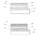
図1(A)は、本発明の一態様における光電変換装置の断面図の一例である。該光電変換装置は、透光性を有する基板100上に、第1の電極110、第1の半導体層131、第2の半導体層132、第3の半導体層133、および第2の電極120を有して構成される。透光性を有する基板100には、例えばガラス基板を用いることができる。
FIG. 1A is an example of a cross-sectional view of a photoelectric conversion device according to one embodiment of the present invention. In the photoelectric conversion device, the
なお、本実施の形態においては、第1の電極110に透光性導電膜を用い、基板100側を受光面とする例を説明するが、第2の電極120に透光性導電膜を用いれば、第2の電極120側を受光面とすることができる。また、第1の電極110および第2の電極120の両方に透光性導電膜を用いれば、両面を受光面とすることができる。なお、第2の電極120側のみを受光面とする場合は、基板100に透光性はなくてもよい。
Note that although an example in which a light-transmitting conductive film is used for the
また、図示した構成に限らず、第1の半導体層131と第3の半導体層133を入れ替えた構造としてもよい。また、図2に示すように、第1の電極110と第1の半導体層131との間に第1のバッファ層141、および第2の電極120と第3の半導体層133との間にバッファ層142を設けてもよい。該バッファ層は、半導体層と電極との間のコンタクト特性を改善する効果があり、導電性または半導体特性を有する酸化亜鉛、酸化ニッケル、酸化モリブデンなどの金属酸化物や、ポリエチレンジオキシチオフェン/ポリスチレンスルフォン酸(略称:PEDOT/PSS)などの導電性高分子を用いることができる。なお、第1のバッファ層141、または第2のバッファ層142のどちらか一方が設けられている構成であってもよい。また、第1のバッファ層141、および第2のバッファ層142は異なる材料であってもよい。
Further, the structure is not limited to the illustrated structure, and the
また、図1(B)では、第1の電極110の表面に凹凸加工を施した例を示している。第1の半導体層131、第2の半導体層132、第3の半導体層133、および第2の電極120は、図示したように第1の電極110の表面凹凸を反映した形状となる。凹凸加工された面では入射光が多重反射し、光電変換領域内には光が斜めに進行することから光路長が増大する。また、裏面反射光が表面で全反射する、所謂光閉じ込め効果を起こさせることもできる。
Further, FIG. 1B shows an example in which the surface of the
なお、上記透光性導電膜には、例えば、インジウム錫酸化物、珪素を含むインジウム錫酸化物、亜鉛を含む酸化インジウム、酸化亜鉛、ガリウムを含む酸化亜鉛、アルミニウムを含む酸化亜鉛、酸化錫、フッ素を含む酸化錫、アンチモンを含む酸化錫、またはグラフェン等を用いることができる。また、透光性導電膜は単層に限らず、異なる膜の積層でもよい。 The translucent conductive film includes, for example, indium tin oxide, indium tin oxide containing silicon, indium oxide containing zinc, zinc oxide, zinc oxide containing gallium, zinc oxide containing aluminum, tin oxide, Tin oxide containing fluorine, tin oxide containing antimony, graphene, or the like can be used. Further, the translucent conductive film is not limited to a single layer, and may be a stack of different films.
第1の半導体層131には、p型の導電型を有する透光性半導体層を用いることができる。また、本発明の一態様における透光性半導体層は、無機化合物と有機化合物の複合材料である。
As the
該無機化合物としては、バンドギャップが2eV以上、好ましくは3eV以上である遷移金属酸化物を用いることができる。特に元素周期表における第4族乃至第8族に属する金属の酸化物であることが好ましい。 As the inorganic compound, a transition metal oxide having a band gap of 2 eV or more, preferably 3 eV or more can be used. In particular, an oxide of a metal belonging to Groups 4 to 8 in the periodic table is preferable.
例えば、該無機化合物としては、酸化バナジウム、酸化ニオブ、酸化タンタル、酸化クロム、酸化モリブデン、酸化タングステン、酸化マンガン、酸化レニウム、酸化チタンなどを用いることができる。中でも特に、酸化モリブデンは大気中でも安定であり、吸湿性が低く、扱いやすいため好ましい。 For example, as the inorganic compound, vanadium oxide, niobium oxide, tantalum oxide, chromium oxide, molybdenum oxide, tungsten oxide, manganese oxide, rhenium oxide, titanium oxide, or the like can be used. Among these, molybdenum oxide is especially preferable because it is stable in the air, has a low hygroscopic property, and is easy to handle.
また、上記有機化合物としては、バンドギャップが2eV以上、好ましくは3eV以上である材料を用いることが好ましい。 As the organic compound, it is preferable to use a material having a band gap of 2 eV or more, preferably 3 eV or more.
また、該有機化合物としては、正孔輸送性が高いことが好ましい。具体的には、10−6cm2/Vs以上の正孔移動度を有する物質であることが好ましい。但し、電子よりも正孔の輸送性の高い物質であれば、これら以外のものを用いてもよい。 The organic compound preferably has a high hole transport property. Specifically, a substance having a hole mobility of 10 −6 cm 2 / Vs or higher is preferable. Note that other than these substances, any substance that has a property of transporting more holes than electrons may be used.
例えば、該有機化合物としては、芳香族アミン化合物、カルバゾール誘導体、芳香族炭化水素、高分子化合物(オリゴマー、デンドリマー、ポリマー等)、ジベンゾフラン骨格もしくはジベンゾチオフェン骨格を含む複素環化合物など、種々の化合物を用いることができる。 Examples of the organic compound include various compounds such as aromatic amine compounds, carbazole derivatives, aromatic hydrocarbons, polymer compounds (oligomers, dendrimers, polymers, etc.), heterocyclic compounds containing a dibenzofuran skeleton or a dibenzothiophene skeleton. Can be used.
上述した無機化合物および有機化合物を用いることにより、透光性の高い複合材料を形成することができる。 By using the inorganic compound and the organic compound described above, a highly light-transmitting composite material can be formed.
また、上述の遷移金属酸化物は電子受容性を有し、正孔輸送性の高い有機化合物との複合材料はキャリア密度が高く、p型の半導体特性を示す。また、該複合材料は、可視光域から赤外域の広い波長範囲に渡って透過率が高い特性を有している。また、該複合材料は、屈折率がインジウム錫酸化物などの透光性導電膜と近く、膜厚を適切に調整することによって、反射防止膜として作用させることができる。 In addition, the above-described transition metal oxide has an electron accepting property, and a composite material with an organic compound having a high hole transporting property has a high carrier density and exhibits p-type semiconductor characteristics. In addition, the composite material has a characteristic of high transmittance over a wide wavelength range from the visible light region to the infrared region. The composite material has a refractive index close to that of a light-transmitting conductive film such as indium tin oxide, and can function as an antireflection film by adjusting the film thickness appropriately.
また、該複合材料は、共蒸着を用いて形成することができる。また塗布法、またはゾルゲル法などを用いて形成することもできる。有機化合物に対する無機化合物のモル比を大きくすると、電荷移動帯の吸光度が増大する、即ちより多くの分子が励起状態になる傾向にあるが、電荷輸送性は有機化合物と無機化合物の組み合わせにも依存するので、モル比は適宜決めるのが最良である。該複合材料の厚さは、1nm〜50nmにすることが好ましい。 The composite material can be formed by co-evaporation. It can also be formed using a coating method or a sol-gel method. Increasing the molar ratio of the inorganic compound to the organic compound increases the absorbance of the charge transfer band, that is, more molecules tend to be in an excited state, but the charge transportability also depends on the combination of the organic compound and the inorganic compound Therefore, it is best to determine the molar ratio appropriately. The thickness of the composite material is preferably 1 nm to 50 nm.
従来の有機半導体を用いた光電変換装置では、例えば透光性が不十分なフタロシアニンを窓層としていたため、窓層における光吸収損失が発生していたが、本発明の一態様における透光性を有する該複合材料を窓層に用いることにより、窓層での光吸収損失が低減し、光吸収領域において効率良く光電変換を行うことできるようになる。 In a conventional photoelectric conversion device using an organic semiconductor, for example, phthalocyanine having insufficient translucency was used as a window layer, and thus a light absorption loss occurred in the window layer, but the translucency in one embodiment of the present invention By using the composite material having a for the window layer, light absorption loss in the window layer is reduced, and photoelectric conversion can be efficiently performed in the light absorption region.
図3には、従来の窓層の一例である亜鉛フタロシアニン(ZnPc)と、本発明の一態様である無機化合物と有機化合物の複合材料として、4,4’−ジ(N−カルバゾリル)ビフェニル(略称:CBP)および酸化モリブデンの複合材料(混合比 CBP:MoOx=1:1)、4,4’−ビス{N−[4−ジ(m−トリル)アミノ]フェニル−N−フェニルアミノ}ビフェニル(略称:DNTPD)および酸化モリブデンの複合材料(混合比 DNTPD:MoOx=1:2)、4,4’−ビス[N−(1−ナフチル)−N−フェニル−アミノ]−ビフェニル(略称:NPD)および酸化モリブデンの複合材料(混合比 NPB:MoOx=1:2)との透過率の比較結果を示す。本発明の一態様である無機化合物と有機化合物の複合材料は、従来の窓層の一例である亜鉛フタロシアニンに比べて透過率は非常に高く、窓層における光吸収損失を低減できることを示唆している。また、広い波長範囲で透過率が高いため、膜厚を厚く形成することができ、横方向の抵抗の低減および上下電極などによる縦方向のショートを防止することができる。また、該複合材料を窓層として用いる場合は、半導体層とのコンタクト抵抗が低いため、図2に例示した窓層と接するバッファ層は省くことができる。 In FIG. 3, as a composite material of zinc phthalocyanine (ZnPc) which is an example of a conventional window layer and an inorganic compound and an organic compound which is one embodiment of the present invention, 4,4′-di (N-carbazolyl) biphenyl ( Abbreviation: CBP) and molybdenum oxide composite (mixing ratio CBP: MoOx = 1: 1), 4,4′-bis {N- [4-di (m-tolyl) amino] phenyl-N-phenylamino} biphenyl (Abbreviation: DNTPD) and a composite material of molybdenum oxide (mixing ratio DNTPD: MoOx = 1: 2), 4,4′-bis [N- (1-naphthyl) -N-phenyl-amino] -biphenyl (abbreviation: NPD) ) And molybdenum oxide composite material (mixing ratio NPB: MoOx = 1: 2). The composite material of an inorganic compound and an organic compound which is one embodiment of the present invention has a very high transmittance compared to zinc phthalocyanine which is an example of a conventional window layer, suggesting that light absorption loss in the window layer can be reduced. Yes. Further, since the transmittance is high in a wide wavelength range, the film thickness can be increased, and resistance in the lateral direction can be reduced and a vertical short circuit caused by the upper and lower electrodes can be prevented. Further, when the composite material is used as a window layer, the contact resistance with the semiconductor layer is low, so that the buffer layer in contact with the window layer illustrated in FIG. 2 can be omitted.
第3の半導体層133には、n型の導電型を有する半導体層を用いることができる。第3の半導体層133の厚さは10nm〜50nmが好ましく、共蒸着法、塗布法、ゾルゲル法などを適宜用いて形成することができる。第3の半導体層133は、電子輸送性の有機化合物であることが好ましく、さらに好ましくは芳香環を含むキレート配位子を有するキレート金属錯体、またはフェナントロリン骨格を有する有機化合物、またはオキサジアゾール骨格を有する有機化合物や、ペリレン誘導体、ナフタレン誘導体、キノン類、メチルビオロゲン、フラーレン等が挙げられる。具体的には、トリス(8−キノリノラト)アルミニウム(略称:Alq3)、トリス(4−メチル−8−キノリノラト)アルミニウム(略称:Almq3)、ビス(10−ヒドロキシベンゾ[h]−キノリナト)ベリリウム(略称:BeBq2)、ビス(2−メチル−8−キノリノラト)(4−フェニルフェノラト)アルミニウム(略称:BAlq)、ビス[2−(2’−ヒドロキシフェニル)ベンズオキサゾラト]亜鉛(略称:Zn(BOX)2)、ビス[2−(2’−ヒドロキシフェニル)ベンゾチアゾラト]亜鉛(略称:Zn(BTZ)2)、バソフェナントロリン(略称:BPhen)、バソキュプロイン(略称:BCP)、2−(4−ビフェニリル)−5−(4−tert−ブチルフェニル)−1,3,4−オキサジアゾール(略称:PBD)、1,3−ビス[5−(4−tert−ブチルフェニル)−1,3,4−オキサジアゾール−2−イル]ベンゼン(略称:OXD−7)、2,2’,2’’−(1,3,5−ベンゼントリイル)−トリス(1−フェニル−1H−ベンゾイミダゾール)(略称:TPBI)、3−(4−ビフェニリル)−4−フェニル−5−(4−tert−ブチルフェニル)−1,2,4−トリアゾール(略称:TAZ)、3−(4−ビフェニリル)−4−(4−エチルフェニル)−5−(4−tert−ブチルフェニル)−1,2,4−トリアゾール(略称:p−EtTAZ)、フェニルC61酪酸メチルエステル(略称:PCBM)、ナフタレン−2,3,6,7−テトラカルボン酸二無水物(略称:NTCDA)などが挙げられるが、これらに限定されることはない。また、上述した化合物の中でも、ペリレン誘導体、ナフタレン誘導体、キノン類、メチルビオロゲン、フラーレン等は、電子キャリアを発生しやすく、第3の半導体層133として好適な化合物群である。
As the
第2の半導体層132には、i型の導電型を有する半導体層を用いることができる。第2の半導体層132は、上述したn型の導電型を有する有機半導体材料と、p型の導電型を有する有機半導体材料とを共蒸着することによって得ることができる。第3の半導体層133の厚さは1nm〜1000nmとすることが好ましい。
As the
代表的なp型の有機半導体材料としては、フタロシアニン(略称:H2Pc)、銅フタロシアニン(略称:CuPc)、亜鉛フタロシアニン(略称:ZnPc)、錫フタロシアニン(略称:SnPc)バナジルフタロシアニン(略称:VOPc)、4,4’−ビス[N−(1−ナフチル)−N−フェニル−アミノ]−ビフェニル(略称:NPD)、4,4’,4’’−トリス(N,N−ジフェニルアミノ)トリフェニルアミン(略称:TDATA)、4,4’,4’’−トリス[N−(3−メチルフェニル)−N−フェニル−アミノ]−トリフェニルアミン(m−TDATA)、4,4’,4’’−トリス[N−(3−メチルフェニル)−N−フェニルアミノ]トリフェニルアミン(略称:MTDATA)、1,3,5−トリス[N,N−ジ(m−トリル)アミノ]ベンゼン(略称:m−MTDAB)、N,N’−ジフェニル−N,N’−ビス(3−メチルフェニル)−1,1’−ビフェニル−4,4’−ジアミン(略称:TPD)、4,4’−ビス[N−(1−ナフチル)−N−フェニルアミノ]ビフェニル(略称:NPB)、4,4’−ビス{N−[4−ジ(m−トリル)アミノ]フェニル−N−フェニルアミノ}ビフェニル(略称:DNTPD)、4,4’,4’’−トリス(N−カルバゾリル)トリフェニルアミン(略称:TCTA)、ポリエチレンジオキシチオフェン/ポリスチレンスルフォン酸(略称:PEDOT/PSS)、ポリ−3−ヘキシルチオフェン(略称:P3HT)、ポリ(N−ドデシル−2,5,−ビス(2’−チエニル)ピロール−2,1,3−ベンゾチアジアゾール)(略称:PTPTB)、ポリ[2,1,3−ベンゾチアジアゾール−4,7−ジイル[4,4−ビス(2−エチルヘキシル)−4H−シクロペンタ[2,1−b:3,4−b’]ジチオフェン−2,6−ジイル]](略称:PCPTBT)、ポリ(2−メトキシ−5−(3’,7’−ジメチルオクチルオキシ)−1,4−フェニレン−ビニレン)(略称:MDMO−PPV)、パーフルオロオクタン酸のアンモニウム塩(略称:APFO)、ポリチエノチオフェン−ベンゾチオフェン(略称:PTB1)などが挙げられるが、これらに限定されることはない。また、上述した化合物の中でも、NPD、TDATA、MTDATA、m−MTDAB、TPD、NPB、DNTPD、TCTAなどに代表される芳香族アミン化合物は、正孔キャリアを発生しやすく、p型の有機半導体材料として好適な化合物群である。 As typical p-type organic semiconductor materials, phthalocyanine (abbreviation: H 2 Pc), copper phthalocyanine (abbreviation: CuPc), zinc phthalocyanine (abbreviation: ZnPc), tin phthalocyanine (abbreviation: SnPc) vanadyl phthalocyanine (abbreviation: VOPc) ), 4,4′-bis [N- (1-naphthyl) -N-phenyl-amino] -biphenyl (abbreviation: NPD), 4,4 ′, 4 ″ -tris (N, N-diphenylamino) tri Phenylamine (abbreviation: TDATA), 4,4 ′, 4 ″ -tris [N- (3-methylphenyl) -N-phenyl-amino] -triphenylamine (m-TDATA), 4,4 ′, 4 '' -Tris [N- (3-methylphenyl) -N-phenylamino] triphenylamine (abbreviation: MTDATA), 1,3,5-tris [N, N-di (m-tolyl) Amino] benzene (abbreviation: m-MTDAB), N, N′-diphenyl-N, N′-bis (3-methylphenyl) -1,1′-biphenyl-4,4′-diamine (abbreviation: TPD), 4,4′-bis [N- (1-naphthyl) -N-phenylamino] biphenyl (abbreviation: NPB), 4,4′-bis {N- [4-di (m-tolyl) amino] phenyl-N -Phenylamino} biphenyl (abbreviation: DNTPD), 4,4 ′, 4 ″ -tris (N-carbazolyl) triphenylamine (abbreviation: TCTA), polyethylenedioxythiophene / polystyrene sulfonic acid (abbreviation: PEDOT / PSS) , Poly-3-hexylthiophene (abbreviation: P3HT), poly (N-dodecyl-2,5, -bis (2′-thienyl) pyrrole-2,1,3-benzothiadiazole) (abbreviation: TPTB), poly [2,1,3-benzothiadiazole-4,7-diyl [4,4-bis (2-ethylhexyl) -4H-cyclopenta [2,1-b: 3,4-b ′] dithiophene- 2,6-diyl]] (abbreviation: PCPTBT), poly (2-methoxy-5- (3 ′, 7′-dimethyloctyloxy) -1,4-phenylene-vinylene) (abbreviation: MDMO-PPV), par Examples include ammonium salt of fluorooctanoic acid (abbreviation: APFO) and polythienothiophene-benzothiophene (abbreviation: PTB1), but are not limited thereto. Among the compounds described above, aromatic amine compounds typified by NPD, TDATA, MTDATA, m-MTDAB, TPD, NPB, DNTPD, TCTA, etc. are likely to generate hole carriers, and are p-type organic semiconductor materials. As a preferred group of compounds.
上述した第1の半導体層131、第2の半導体層132、第3の半導体層133により、pin接合を形成することができる。また、n型の導電型を有する半導体層と、p型の導電型を有する半導体層との混合によって得られるi型の半導体層である第3の半導体層133は、光吸収層として光電変換に寄与する。
The
第2の電極120は、銀、アルミニウム、銅などの低抵抗金属を用いることができ、スパッタ法や真空蒸着法などで形成することができる。または、スクリーン印刷法を用いて、銀ペーストや、銅ペーストなどの導電性樹脂で形成しても良い。また、前述したように透光性導電膜を用いることもできる。
The
なお、図4に示すように、窓層であるp型半導体層を2層とする構成としてもよい。図4に示す光電変換装置は、透光性を有する基板200上に、第1の電極210、第1の半導体層231、第2の半導体層232、第3の半導体層233、第4の半導体層234、および第2の電極220を有して構成される。
In addition, as shown in FIG. 4, it is good also as a structure which makes the p-type semiconductor layer which is a window layer into two layers. In the photoelectric conversion device illustrated in FIG. 4, the
基板200、第1の電極210、第1の半導体層231、第2の電極220のそれぞれは、図1構成の説明で記した基板100、第1の電極110、第1の半導体層131、第2の電極120のそれぞれと同じ材料を用いることができる。
Each of the
また、第3の半導体層233は、図1の構成で説明した第2の半導体層132と同じ材料を用いることができ、第4の半導体層234は、第3の半導体層133と同じ材料を用いることができる。
The
第2の半導体層232はp型の半導体特性を示す有機化合物から構成されており、前述したp型の有機半導体材料に例示した材料を用いることができる。
The
このように、窓層であるp型半導体層を2層とするためのプロセスを行うことで、ピンホール生成の機会を低減させることができ、上下電極間のショートなどの不良を低減させることができる。なお、図4の光電変換装置の構成に、図1(B)の光電変換装置の構成、および/または図2の光電変換装置の構成を組み合わすこともできる。 Thus, by performing the process for making the p-type semiconductor layer that is the window layer into two layers, the opportunity for pinhole generation can be reduced, and defects such as a short circuit between the upper and lower electrodes can be reduced. it can. Note that the structure of the photoelectric conversion device in FIG. 4 can be combined with the structure of the photoelectric conversion device in FIG. 1B and / or the structure of the photoelectric conversion device in FIG.
以上の構成の構成を用いることにより、窓層における光吸収損失が少なく、上下電極間のショートが起きにくい光電変換装置とすることができる。 By using the above-described configuration, a photoelectric conversion device with a small light absorption loss in the window layer and a short circuit between the upper and lower electrodes hardly occurs.
本実施の形態は、他の実施の形態と自由に組み合わすことができる。 This embodiment can be freely combined with any of the other embodiments.
(実施の形態2)
本実施の形態では、実施の形態1で示した透光性半導体層について説明する。
(Embodiment 2)
In this embodiment, the light-transmitting semiconductor layer described in
実施の形態1で示した光電変換装置における透光性半導体層(第1の半導体層131)には、遷移金属酸化物と有機化合物との複合材料を用いることができる。なお、本明細書中において、複合とは、単に2つの材料を混合させるだけでなく、複数の材料を混合することによって材料間での電荷の授受が行われ得る状態になることを言う。
For the light-transmitting semiconductor layer (first semiconductor layer 131) in the photoelectric conversion device described in
上記遷移金属酸化物としては、電子受容性を有する遷移金属酸化物を用いることができる。また、遷移金属酸化物の中でも、元素周期表における第4族乃至第8族に属する金属の酸化物であり、バンドギャップが2eV以上、好ましくは3eV以上であることが好ましい。 As the transition metal oxide, a transition metal oxide having an electron accepting property can be used. Further, among transition metal oxides, oxides of metals belonging to Groups 4 to 8 in the periodic table, and a band gap is preferably 2 eV or more, preferably 3 eV or more.
例えば、該遷移金属酸化物としては、電子受容性の高い、酸化バナジウム、酸化ニオブ、酸化タンタル、酸化クロム、酸化モリブデン、酸化タングステン、酸化マンガン、酸化レニウム、酸化チタンなどを用いることができる。中でも特に、酸化モリブデンは大気中でも安定であり、吸湿性が低く、扱いやすいため好ましい。 For example, as the transition metal oxide, vanadium oxide, niobium oxide, tantalum oxide, chromium oxide, molybdenum oxide, tungsten oxide, manganese oxide, rhenium oxide, titanium oxide, or the like with high electron accepting property can be used. Among these, molybdenum oxide is especially preferable because it is stable in the air, has a low hygroscopic property, and is easy to handle.
また、上記有機化合物としては、バンドギャップ(最高被占有軌道準位(HOMO準位)と最低空軌道準位(LUMO準位)とのエネルギー差)が2eV以上、好ましくは3eV以上である材料を用いることが好ましい。 The organic compound is a material having a band gap (energy difference between the highest occupied orbital level (HOMO level) and the lowest unoccupied orbital level (LUMO level)) of 2 eV or more, preferably 3 eV or more. It is preferable to use it.
また、該有機化合物としては、正孔輸送性が高いことが好ましい。具体的には、10−6cm2/Vs以上の正孔移動度を有する物質であることが好ましい。但し、電子よりも正孔の輸送性の高い物質であれば、これら以外のものを用いてもよい。 The organic compound preferably has a high hole transport property. Specifically, a substance having a hole mobility of 10 −6 cm 2 / Vs or higher is preferable. Note that other than these substances, any substance that has a property of transporting more holes than electrons may be used.
例えば、該有機化合物としては、芳香族アミン化合物、カルバゾール誘導体、芳香族炭化水素、高分子化合物(オリゴマー、デンドリマー、ポリマー等)、ジベンゾフラン骨格もしくはジベンゾチオフェン骨格を含む複素環化合物など、種々の化合物を用いることができる。 Examples of the organic compound include various compounds such as aromatic amine compounds, carbazole derivatives, aromatic hydrocarbons, polymer compounds (oligomers, dendrimers, polymers, etc.), heterocyclic compounds containing a dibenzofuran skeleton or a dibenzothiophene skeleton. Can be used.
上述した無機化合物および有機化合物を用いることにより、透光性の高い複合材料を形成することができる。 By using the inorganic compound and the organic compound described above, a highly light-transmitting composite material can be formed.
上記遷移金属酸化物と上記有機化合物とを含む複合材料では、有機化合物の最高被占有軌道準位(HOMO準位)にある電子が、遷移金属酸化物の伝導帯に移動することにより、遷移金属酸化物と有機化合物との間に相互作用が生じる。この相互作用により、遷移金属酸化物と有機化合物とを含む複合材料は、キャリア濃度が高く、p型の半導体特性を示す。 In the composite material including the transition metal oxide and the organic compound, electrons in the highest occupied orbital level (HOMO level) of the organic compound move to the conduction band of the transition metal oxide, whereby the transition metal Interaction occurs between the oxide and the organic compound. By this interaction, the composite material including the transition metal oxide and the organic compound has a high carrier concentration and exhibits p-type semiconductor characteristics.
以下では、複合材料に用いることのできる有機化合物を具体的に列挙する。 Below, the organic compound which can be used for a composite material is listed concretely.
例えば、複合材料に用いることのできる芳香族アミン化合物としては、例えば、4,4’−ビス[N−(1−ナフチル)−N−フェニルアミノ]ビフェニル(略称:NPB)、N,N’−ビス(3−メチルフェニル)−N,N’−ジフェニル−[1,1’−ビフェニル]−4,4’−ジアミン(略称:TPD)、4,4’,4’’−トリス(N,N−ジフェニルアミノ)トリフェニルアミン(略称:TDATA)、4,4’,4’’−トリス[N−(3−メチルフェニル)−N−フェニルアミノ]トリフェニルアミン(略称:MTDATA)、N,N’−ビス(スピロ−9,9’−ビフルオレン−2−イル)−N,N’−ジフェニルベンジジン(略称:BSPB)等を用いることができる。また、N,N’−ビス(4−メチルフェニル)−N,N’−ジフェニル−p−フェニレンジアミン(略称:DTDPPA)、4,4’−ビス[N−(4−ジフェニルアミノフェニル)−N−フェニルアミノ]ビフェニル(略称:DPAB)、N,N’−ビス[4−[ビス(3−メチルフェニル)アミノ]フェニル]−N,N’−ジフェニル−[1,1’−ビフェニル]−4,4’−ジアミン(略称:DNTPD)、1,3,5−トリス[N−(4−ジフェニルアミノフェニル)−N−フェニルアミノ]ベンゼン(略称:DPA3B)、4−フェニル−4’−(9−フェニルフルオレン−9−イル)トリフェニルアミン(略称:BPAFLP)、4,4’−ビス[N−(9,9−ジメチルフルオレン−2−イル)−N−フェニルアミノ]ビフェニル(略称:DFLDPBi)、4,4’−ビス[N−(スピロ−9,9’−ビフルオレン−2−イル)−N―フェニルアミノ]ビフェニル(略称:BSPB)等を挙げることができる。 For example, as an aromatic amine compound that can be used for the composite material, for example, 4,4′-bis [N- (1-naphthyl) -N-phenylamino] biphenyl (abbreviation: NPB), N, N′— Bis (3-methylphenyl) -N, N′-diphenyl- [1,1′-biphenyl] -4,4′-diamine (abbreviation: TPD), 4,4 ′, 4 ″ -tris (N, N -Diphenylamino) triphenylamine (abbreviation: TDATA), 4,4 ', 4 "-tris [N- (3-methylphenyl) -N-phenylamino] triphenylamine (abbreviation: MTDATA), N, N '-Bis (spiro-9,9'-bifluoren-2-yl) -N, N'-diphenylbenzidine (abbreviation: BSPB) or the like can be used. N, N′-bis (4-methylphenyl) -N, N′-diphenyl-p-phenylenediamine (abbreviation: DTDPPA), 4,4′-bis [N- (4-diphenylaminophenyl) -N -Phenylamino] biphenyl (abbreviation: DPAB), N, N'-bis [4- [bis (3-methylphenyl) amino] phenyl] -N, N'-diphenyl- [1,1'-biphenyl] -4 , 4′-diamine (abbreviation: DNTPD), 1,3,5-tris [N- (4-diphenylaminophenyl) -N-phenylamino] benzene (abbreviation: DPA3B), 4-phenyl-4 ′-(9 -Phenylfluoren-9-yl) triphenylamine (abbreviation: BPAFLP), 4,4'-bis [N- (9,9-dimethylfluoren-2-yl) -N-phenylamino] biphe Le (abbreviation: DFLDPBi), 4,4'-bis [N- (spiro-9,9'-bifluoren-2-yl) -N- phenylamino] biphenyl (abbreviation: BSPB), and the like.
複合材料に用いることのできるカルバゾール誘導体としては、具体的には、3−[N−(9−フェニルカルバゾール−3−イル)−N−フェニルアミノ]−9−フェニルカルバゾール(略称:PCzPCA1)、3,6−ビス[N−(9−フェニルカルバゾール−3−イル)−N−フェニルアミノ]−9−フェニルカルバゾール(略称:PCzPCA2)、3−[N−(1−ナフチル)−N−(9−フェニルカルバゾール−3−イル)アミノ]−9−フェニルカルバゾール(略称:PCzPCN1)等を挙げることができる。 Specific examples of the carbazole derivative that can be used for the composite material include 3- [N- (9-phenylcarbazol-3-yl) -N-phenylamino] -9-phenylcarbazole (abbreviation: PCzPCA1), 3 , 6-Bis [N- (9-phenylcarbazol-3-yl) -N-phenylamino] -9-phenylcarbazole (abbreviation: PCzPCA2), 3- [N- (1-naphthyl) -N- (9- Phenylcarbazol-3-yl) amino] -9-phenylcarbazole (abbreviation: PCzPCN1) and the like.
また、複合材料に用いることのできる他のカルバゾール誘導体としては、4,4’−ジ(N−カルバゾリル)ビフェニル(略称:CBP)、1,3,5−トリス[4−(N−カルバゾリル)フェニル]ベンゼン(略称:TCPB)、9−[4−(N−カルバゾリル)フェニル]−10−フェニルアントラセン(略称:CzPA)、1,4−ビス[4−(N−カルバゾリル)フェニル]−2,3,5,6−テトラフェニルベンゼン等を用いることができる。 Other carbazole derivatives that can be used for the composite material include 4,4′-di (N-carbazolyl) biphenyl (abbreviation: CBP), 1,3,5-tris [4- (N-carbazolyl) phenyl. ] Benzene (abbreviation: TCPB), 9- [4- (N-carbazolyl) phenyl] -10-phenylanthracene (abbreviation: CzPA), 1,4-bis [4- (N-carbazolyl) phenyl] -2,3 , 5,6-tetraphenylbenzene or the like can be used.
複合材料に用いることのできる芳香族炭化水素としては、例えば、2−tert−ブチル−9,10−ジ(2−ナフチル)アントラセン(略称:t−BuDNA)、2−tert−ブチル−9,10−ジ(1−ナフチル)アントラセン、9,10−ビス(3,5−ジフェニルフェニル)アントラセン(略称:DPPA)、2−tert−ブチル−9,10−ビス(4−フェニルフェニル)アントラセン(略称:t−BuDBA)、9,10−ジ(2−ナフチル)アントラセン(略称:DNA)、9,10−ジフェニルアントラセン(略称:DPAnth)、2−tert−ブチルアントラセン(略称:t−BuAnth)、9,10−ビス(4−メチル−1−ナフチル)アントラセン(略称:DMNA)、9,10−ビス[2−(1−ナフチル)フェニル]−2−tert−ブチル−アントラセン、9,10−ビス[2−(1−ナフチル)フェニル]アントラセン、2,3,6,7−テトラメチル−9,10−ジ(1−ナフチル)アントラセン、2,3,6,7−テトラメチル−9,10−ジ(2−ナフチル)アントラセン、9,9’−ビアントリル、10,10’−ジフェニル−9,9’−ビアントリル、10,10’−ビス(2−フェニルフェニル)−9,9’−ビアントリル、10,10’−ビス[(2,3,4,5,6−ペンタフェニル)フェニル]−9,9’−ビアントリル、アントラセン、テトラセン、ルブレン、ペリレン、2,5,8,11−テトラ(tert−ブチル)ペリレン等が挙げられる。また、この他、ペンタセン、コロネン等も用いることができる。このように、1×10−6cm2/Vs以上の正孔移動度を有し、炭素数14〜42である芳香族炭化水素を用いることがより好ましい。 Examples of aromatic hydrocarbons that can be used for the composite material include 2-tert-butyl-9,10-di (2-naphthyl) anthracene (abbreviation: t-BuDNA), 2-tert-butyl-9,10. -Di (1-naphthyl) anthracene, 9,10-bis (3,5-diphenylphenyl) anthracene (abbreviation: DPPA), 2-tert-butyl-9,10-bis (4-phenylphenyl) anthracene (abbreviation: t-BuDBA), 9,10-di (2-naphthyl) anthracene (abbreviation: DNA), 9,10-diphenylanthracene (abbreviation: DPAnth), 2-tert-butylanthracene (abbreviation: t-BuAnth), 9, 10-bis (4-methyl-1-naphthyl) anthracene (abbreviation: DMNA), 9,10-bis [2- (1-naphthy ) Phenyl] -2-tert-butyl-anthracene, 9,10-bis [2- (1-naphthyl) phenyl] anthracene, 2,3,6,7-tetramethyl-9,10-di (1-naphthyl) Anthracene, 2,3,6,7-tetramethyl-9,10-di (2-naphthyl) anthracene, 9,9′-bianthryl, 10,10′-diphenyl-9,9′-bianthryl, 10,10 ′ -Bis (2-phenylphenyl) -9,9'-bianthryl, 10,10'-bis [(2,3,4,5,6-pentaphenyl) phenyl] -9,9'-bianthryl, anthracene, tetracene , Rubrene, perylene, 2,5,8,11-tetra (tert-butyl) perylene, and the like. In addition, pentacene, coronene, and the like can also be used. Thus, it is more preferable to use an aromatic hydrocarbon having a hole mobility of 1 × 10 −6 cm 2 / Vs or more and having 14 to 42 carbon atoms.
複合材料に用いることのできる芳香族炭化水素は、ビニル骨格を有していてもよい。ビニル基を有している芳香族炭化水素としては、例えば、4,4’−ビス(2,2−ジフェニルビニル)ビフェニル(略称:DPVBi)、9,10−ビス[4−(2,2−ジフェニルビニル)フェニル]アントラセン(略称:DPVPA)等が挙げられる。 The aromatic hydrocarbon that can be used for the composite material may have a vinyl skeleton. As the aromatic hydrocarbon having a vinyl group, for example, 4,4′-bis (2,2-diphenylvinyl) biphenyl (abbreviation: DPVBi), 9,10-bis [4- (2,2- Diphenylvinyl) phenyl] anthracene (abbreviation: DPVPA) and the like.
また、複合材料に用いることのできる有機化合物は、ジベンゾフラン骨格もしくはジベンゾチオフェン骨格を含む複素環化合物であっても良い。 The organic compound that can be used for the composite material may be a heterocyclic compound including a dibenzofuran skeleton or a dibenzothiophene skeleton.
また、複合材料に用いることのできる有機化合物は、高分子化合物であってもよく、例えば、ポリ(N−ビニルカルバゾール)(略称:PVK)、ポリ(4−ビニルトリフェニルアミン)(略称:PVTPA)、ポリ[N−(4−{N’−[4−(4−ジフェニルアミノ)フェニル]フェニル−N’−フェニルアミノ}フェニル)メタクリルアミド](略称:PTPDMA)ポリ[N,N’−ビス(4−ブチルフェニル)−N,N’−ビス(フェニル)ベンジジン](略称:Poly−TPD)などを用いても良い。 The organic compound that can be used for the composite material may be a high molecular compound, such as poly (N-vinylcarbazole) (abbreviation: PVK), poly (4-vinyltriphenylamine) (abbreviation: PVTPA). ), Poly [N- (4- {N ′-[4- (4-diphenylamino) phenyl] phenyl-N′-phenylamino} phenyl) methacrylamide] (abbreviation: PTPDMA) poly [N, N′-bis (4-Butylphenyl) -N, N′-bis (phenyl) benzidine] (abbreviation: Poly-TPD) or the like may be used.
透光性半導体層の形成方法としては、乾式法、湿式法を問わず、種々の方法を用いることができる。また、各層ごとに異なる成膜方法を用いて形成しても構わない。乾式法としては、例えば、複数の蒸着源から複数の蒸着材料を気化させて成膜する共蒸着法などが挙げられる。また、湿式法としては、ゾルゲル法などを用いて複合材料を含む組成物を調整し、インクジェット法またはスピンコート法などを用いて成膜することができる。 Various methods can be used for forming the light-transmitting semiconductor layer regardless of a dry method or a wet method. Further, each layer may be formed using a different film formation method. Examples of the dry method include a co-evaporation method in which a plurality of evaporation materials are vaporized from a plurality of evaporation sources to form a film. As a wet method, a composition containing a composite material can be adjusted using a sol-gel method or the like, and a film can be formed using an inkjet method, a spin coating method, or the like.
以上説明した透光性半導体層を光電変換装置の窓層に用いれば、窓層における光吸収損失が低減し、光電変換装置の電気特性を向上させることができる。また、高い透光性を有し、かつ抵抗が低いため、窓層を厚く形成することができ、上下電極間のショートが起きにくい光電変換装置とすることができる。 When the light-transmitting semiconductor layer described above is used for a window layer of a photoelectric conversion device, light absorption loss in the window layer can be reduced, and electrical characteristics of the photoelectric conversion device can be improved. Further, since it has high translucency and low resistance, the window layer can be formed thick, and a photoelectric conversion device in which a short circuit between the upper and lower electrodes hardly occurs can be obtained.
本実施の形態は、他の実施の形態と自由に組み合わすことができる。 This embodiment can be freely combined with any of the other embodiments.
100 基板
110 第1の電極
120 第2の電極
131 第1の半導体層
132 第2の半導体層
133 第3の半導体層
141 第1のバッファ層
142 第2のバッファ層
200 基板
210 第1の電極
220 第2の電極
231 第1の半導体層
232 第2の半導体層
233 第3の半導体層
234 第4の半導体層
100
Claims (6)
前記第1の電極上に形成された第1の半導体層と、
前記第1の半導体層上に形成された第2の半導体層と、
前記第2の半導体層上に形成された第3の半導体層と、
前記第3の半導体層上に形成された第2の電極と、
を有し、
前記第1の半導体層は、有機化合物および無機化合物を含む透光性半導体層であり、前記第2の半導体層および前記第3の半導体層は、有機化合物を含む半導体層であることを特徴とする光電変換装置。 A first electrode;
A first semiconductor layer formed on the first electrode;
A second semiconductor layer formed on the first semiconductor layer;
A third semiconductor layer formed on the second semiconductor layer;
A second electrode formed on the third semiconductor layer;
Have
The first semiconductor layer is a translucent semiconductor layer containing an organic compound and an inorganic compound, and the second semiconductor layer and the third semiconductor layer are semiconductor layers containing an organic compound. A photoelectric conversion device.
前記第1の電極上に形成された第1の半導体層と、
前記第1の半導体層上に形成された第2の半導体層と、
前記第2の半導体層上に形成された第3の半導体層と、
前記第3の半導体層上に形成された第4の半導体層と、
前記第4の半導体層上に形成された第2の電極と、
を有し、
前記第1の半導体層は、有機化合物および無機化合物を含む透光性半導体層であり、前記第2の半導体層、前記第3の半導体層、および前記第4の半導体層は、有機化合物を含む半導体層であることを特徴とする光電変換装置。 A first electrode;
A first semiconductor layer formed on the first electrode;
A second semiconductor layer formed on the first semiconductor layer;
A third semiconductor layer formed on the second semiconductor layer;
A fourth semiconductor layer formed on the third semiconductor layer;
A second electrode formed on the fourth semiconductor layer;
Have
The first semiconductor layer is a light-transmitting semiconductor layer containing an organic compound and an inorganic compound, and the second semiconductor layer, the third semiconductor layer, and the fourth semiconductor layer contain an organic compound. A photoelectric conversion device comprising a semiconductor layer.
Priority Applications (3)
| Application Number | Priority Date | Filing Date | Title |
|---|---|---|---|
| JP2011195372A JP2013058562A (en) | 2011-09-07 | 2011-09-07 | Photoelectric conversion device |
| US13/602,352 US8994009B2 (en) | 2011-09-07 | 2012-09-04 | Photoelectric conversion device |
| CN2012103280429A CN103000745A (en) | 2011-09-07 | 2012-09-07 | Photoelectric conversion device |
Applications Claiming Priority (1)
| Application Number | Priority Date | Filing Date | Title |
|---|---|---|---|
| JP2011195372A JP2013058562A (en) | 2011-09-07 | 2011-09-07 | Photoelectric conversion device |
Related Child Applications (1)
| Application Number | Title | Priority Date | Filing Date |
|---|---|---|---|
| JP2016053898A Division JP2016106437A (en) | 2016-03-17 | 2016-03-17 | Photoelectric conversion device |
Publications (2)
| Publication Number | Publication Date |
|---|---|
| JP2013058562A true JP2013058562A (en) | 2013-03-28 |
| JP2013058562A5 JP2013058562A5 (en) | 2014-10-09 |
Family
ID=47752417
Family Applications (1)
| Application Number | Title | Priority Date | Filing Date |
|---|---|---|---|
| JP2011195372A Withdrawn JP2013058562A (en) | 2011-09-07 | 2011-09-07 | Photoelectric conversion device |
Country Status (3)
| Country | Link |
|---|---|
| US (1) | US8994009B2 (en) |
| JP (1) | JP2013058562A (en) |
| CN (1) | CN103000745A (en) |
Cited By (2)
| Publication number | Priority date | Publication date | Assignee | Title |
|---|---|---|---|---|
| WO2015190550A1 (en) * | 2014-06-12 | 2015-12-17 | シャープ株式会社 | Organic element |
| JP2017069567A (en) * | 2015-10-01 | 2017-04-06 | エルジー エレクトロニクス インコーポレイティド | Solar cell |
Families Citing this family (8)
| Publication number | Priority date | Publication date | Assignee | Title |
|---|---|---|---|---|
| JP2013058562A (en) * | 2011-09-07 | 2013-03-28 | Semiconductor Energy Lab Co Ltd | Photoelectric conversion device |
| JP5927027B2 (en) | 2011-10-05 | 2016-05-25 | 株式会社半導体エネルギー研究所 | Photoelectric conversion device |
| US9112086B2 (en) | 2011-11-10 | 2015-08-18 | Semiconductor Energy Laboratory Co., Ltd. | Photoelectric conversion device |
| JP6108858B2 (en) | 2012-02-17 | 2017-04-05 | 株式会社半導体エネルギー研究所 | P-type semiconductor material and semiconductor device |
| KR20150019727A (en) * | 2013-08-14 | 2015-02-25 | 삼성에스디아이 주식회사 | Solar cell module and preparation method thereof |
| KR102590315B1 (en) | 2018-05-28 | 2023-10-16 | 삼성전자주식회사 | Organic photoelectric device and image sensor including the same |
| JP2021015963A (en) * | 2019-07-09 | 2021-02-12 | 日本化薬株式会社 | Photoelectric conversion element material and uses thereof |
| CN111599879B (en) | 2020-06-11 | 2022-05-31 | 武汉华星光电技术有限公司 | PIN photosensitive device, manufacturing method thereof and display panel |
Citations (7)
| Publication number | Priority date | Publication date | Assignee | Title |
|---|---|---|---|---|
| JP2006024791A (en) * | 2004-07-08 | 2006-01-26 | International Manufacturing & Engineering Services Co Ltd | Organic element, organic electroluminescent element and organic solar cell |
| JP2006190994A (en) * | 2004-12-06 | 2006-07-20 | Semiconductor Energy Lab Co Ltd | Photoelectric conversion element, solar cell, and optical sensor |
| JP2007180526A (en) * | 2005-11-30 | 2007-07-12 | Semiconductor Energy Lab Co Ltd | Light emitting element, light emitting device and electronic equipment |
| JP2009177158A (en) * | 2007-12-28 | 2009-08-06 | Semiconductor Energy Lab Co Ltd | Photoelectric conversion device and manufacturing method thereof |
| JP2010073989A (en) * | 2008-09-19 | 2010-04-02 | Idemitsu Kosan Co Ltd | Material for organic thin-film solar cell, and organic thin-film solar cell using the same |
| US20110030789A1 (en) * | 2008-02-18 | 2011-02-10 | The Technical University Of Denmark | Air stable photovoltaic device |
| JP2011233692A (en) * | 2010-04-27 | 2011-11-17 | Idemitsu Kosan Co Ltd | Photoelectric converter, organic solar cell and photoelectric conversion apparatus using these |
Family Cites Families (206)
| Publication number | Priority date | Publication date | Assignee | Title |
|---|---|---|---|---|
| US4180618A (en) | 1977-07-27 | 1979-12-25 | Corning Glass Works | Thin silicon film electronic device |
| JPS5756547Y2 (en) | 1979-02-15 | 1982-12-04 | ||
| US4272641A (en) | 1979-04-19 | 1981-06-09 | Rca Corporation | Tandem junction amorphous silicon solar cells |
| US4316049A (en) | 1979-08-28 | 1982-02-16 | Rca Corporation | High voltage series connected tandem junction solar battery |
| US4385199A (en) | 1980-12-03 | 1983-05-24 | Yoshihiro Hamakawa | Photovoltaic cell having a hetero junction of amorphous silicon carbide and amorphous silicon |
| US4388482A (en) | 1981-01-29 | 1983-06-14 | Yoshihiro Hamakawa | High-voltage photovoltaic cell having a heterojunction of amorphous semiconductor and amorphous silicon |
| JPS5858553A (en) | 1981-10-01 | 1983-04-07 | Fuji Photo Film Co Ltd | X-ray sensitive electrophotographic receptor and its manufacture |
| US4496788A (en) | 1982-12-29 | 1985-01-29 | Osaka Transformer Co., Ltd. | Photovoltaic device |
| JPS59124772U (en) | 1983-02-10 | 1984-08-22 | トヨタ自動車株式会社 | power steering |
| US4510344A (en) | 1983-12-19 | 1985-04-09 | Atlantic Richfield Company | Thin film solar cell substrate |
| JPS60152971A (en) | 1984-01-20 | 1985-08-12 | Fuji Electric Corp Res & Dev Ltd | Conductor radiation detector |
| US4950614A (en) | 1984-05-15 | 1990-08-21 | Semiconductor Energy Laboratory Co., Ltd. | Method of making a tandem type semiconductor photoelectric conversion device |
| US4878097A (en) | 1984-05-15 | 1989-10-31 | Eastman Kodak Company | Semiconductor photoelectric conversion device and method for making same |
| US4633034A (en) | 1985-02-08 | 1986-12-30 | Energy Conversion Devices, Inc. | Photovoltaic device and method |
| US4680422A (en) | 1985-10-30 | 1987-07-14 | The Boeing Company | Two-terminal, thin film, tandem solar cells |
| US4665277A (en) | 1986-03-11 | 1987-05-12 | The United States Of America As Represented By The Administrator Of The National Aeronautics And Space Administration | Floating emitter solar cell |
| US4684761A (en) | 1986-04-09 | 1987-08-04 | The Boeing Company | Method for making graded I-III-VI2 semiconductors and solar cell obtained thereby |
| JPS62171172U (en) | 1986-04-22 | 1987-10-30 | ||
| US4740431A (en) | 1986-12-22 | 1988-04-26 | Spice Corporation | Integrated solar cell and battery |
| JPS63157483U (en) | 1987-03-30 | 1988-10-14 | ||
| CA1303194C (en) | 1987-07-21 | 1992-06-09 | Katsumi Nakagawa | Photovoltaic element with a semiconductor layer comprising non-single crystal material containing at least zn, se and h in an amount of 1 to40 atomic % |
| CA1299716C (en) | 1987-11-20 | 1992-04-28 | Katsumi Nakagawa | Pin junction photovoltaic element with p or n-type semiconductor layercomprising non-single crystal material containing zn, se, h in an amount of 1 to 4 atomic % and a dopant and i-type semiconductor layer comprising non-single crystal si(h,f) material |
| CH674596A5 (en) | 1988-02-12 | 1990-06-15 | Sulzer Ag | |
| JPH01227307A (en) | 1988-03-08 | 1989-09-11 | Asahi Glass Co Ltd | Transparent electric conductor |
| JPH02192771A (en) | 1989-01-21 | 1990-07-30 | Canon Inc | Photovoltaic element |
| US5002617A (en) | 1989-01-21 | 1991-03-26 | Canon Kabushiki Kaisha | Pin heterojunction photovoltaic elements with polycrystal AlAs(H,F) semiconductor film |
| US5002618A (en) | 1989-01-21 | 1991-03-26 | Canon Kabushiki Kaisha | Pin heterojunction photovoltaic elements with polycrystal BAs(H,F) semiconductor film |
| JP2829653B2 (en) | 1989-01-21 | 1998-11-25 | キヤノン株式会社 | Photovoltaic element |
| US5061979A (en) | 1989-02-21 | 1991-10-29 | Canon Kabushiki Kaisha | Semiconductor photoelectric device having a matrix wiring section |
| JP2926845B2 (en) | 1990-03-23 | 1999-07-28 | 日本電気株式会社 | Organic thin film EL device |
| US5328519A (en) | 1990-05-07 | 1994-07-12 | Canon Kabushiki Kaisha | Solar cells |
| KR950014609B1 (en) | 1990-08-03 | 1995-12-11 | 캐논 가부시끼가이샤 | Semiconductor device and manufacturing method thereof |
| US5750000A (en) | 1990-08-03 | 1998-05-12 | Canon Kabushiki Kaisha | Semiconductor member, and process for preparing same and semiconductor device formed by use of same |
| DE4029060C2 (en) | 1990-09-13 | 1994-01-13 | Forschungszentrum Juelich Gmbh | Process for the production of components for electronic, electro-optical and optical components |
| US5213628A (en) | 1990-09-20 | 1993-05-25 | Sanyo Electric Co., Ltd. | Photovoltaic device |
| JPH04276665A (en) | 1991-03-04 | 1992-10-01 | Canon Inc | Integrated solar battery |
| JPH04275467A (en) | 1991-03-04 | 1992-10-01 | Sanyo Electric Co Ltd | Phototransistor |
| JPH04299578A (en) | 1991-03-27 | 1992-10-22 | Canon Inc | Photoelectric transducer |
| JP2564481Y2 (en) | 1991-05-21 | 1998-03-09 | 東急車輛製造株式会社 | Underground buried multi-story parking device |
| CA2069038C (en) | 1991-05-22 | 1997-08-12 | Kiyofumi Sakaguchi | Method for preparing semiconductor member |
| JP3048732B2 (en) | 1991-11-25 | 2000-06-05 | 三洋電機株式会社 | Photovoltaic device |
| US5656098A (en) | 1992-03-03 | 1997-08-12 | Canon Kabushiki Kaisha | Photovoltaic conversion device and method for producing same |
| US5248349A (en) | 1992-05-12 | 1993-09-28 | Solar Cells, Inc. | Process for making photovoltaic devices and resultant product |
| JP3073327B2 (en) | 1992-06-30 | 2000-08-07 | キヤノン株式会社 | Deposition film formation method |
| JP2761156B2 (en) | 1992-06-30 | 1998-06-04 | キヤノン株式会社 | Photovoltaic element, method of manufacturing the same, and power generator using the same |
| US6340781B1 (en) | 1992-07-22 | 2002-01-22 | Imperial Chemical Industries Plc | Purification of pentafluoroethane |
| FR2694451B1 (en) | 1992-07-29 | 1994-09-30 | Asulab Sa | Photovoltaic cell. |
| JPH06151801A (en) | 1992-11-13 | 1994-05-31 | Canon Inc | Photoelectric converter and manufacture thereof |
| JP3360919B2 (en) | 1993-06-11 | 2003-01-07 | 三菱電機株式会社 | Method of manufacturing thin-film solar cell and thin-film solar cell |
| JP3106810B2 (en) | 1993-11-04 | 2000-11-06 | 富士電機株式会社 | Method for producing amorphous silicon oxide thin film |
| US5738731A (en) | 1993-11-19 | 1998-04-14 | Mega Chips Corporation | Photovoltaic device |
| JP3571785B2 (en) | 1993-12-28 | 2004-09-29 | キヤノン株式会社 | Method and apparatus for forming deposited film |
| JPH07263731A (en) | 1994-03-22 | 1995-10-13 | Canon Inc | Polycrystalline silicon device |
| JP2984537B2 (en) | 1994-03-25 | 1999-11-29 | キヤノン株式会社 | Photovoltaic element |
| US5635408A (en) | 1994-04-28 | 1997-06-03 | Canon Kabushiki Kaisha | Method of producing a semiconductor device |
| US5668050A (en) | 1994-04-28 | 1997-09-16 | Canon Kabushiki Kaisha | Solar cell manufacturing method |
| JP3464287B2 (en) | 1994-09-05 | 2003-11-05 | 株式会社半導体エネルギー研究所 | Method for manufacturing semiconductor device |
| JPH08102360A (en) | 1994-09-29 | 1996-04-16 | Toyota Central Res & Dev Lab Inc | Orfanic/inorganic complex thin-film electroluminescent element |
| US5780160A (en) | 1994-10-26 | 1998-07-14 | Donnelly Corporation | Electrochromic devices with improved processability and methods of preparing the same |
| JP3381443B2 (en) | 1995-02-02 | 2003-02-24 | ソニー株式会社 | Method for separating semiconductor layer from substrate, method for manufacturing semiconductor device, and method for manufacturing SOI substrate |
| US5736431A (en) | 1995-02-28 | 1998-04-07 | Semiconductor Energy Laboratory Co., Ltd. | Method for producing thin film solar battery |
| TW447144B (en) | 1995-03-27 | 2001-07-21 | Semiconductor Energy Lab | Semiconductor device and a method of manufacturing the same |
| US7075002B1 (en) | 1995-03-27 | 2006-07-11 | Semiconductor Energy Laboratory Company, Ltd. | Thin-film photoelectric conversion device and a method of manufacturing the same |
| JP2824411B2 (en) | 1995-08-25 | 1998-11-11 | 株式会社豊田中央研究所 | Organic thin-film light emitting device |
| WO1997024907A1 (en) | 1995-12-30 | 1997-07-10 | Casio Computer Co., Ltd. | Display device for performing display operation in accordance with signal light and driving method therefor |
| EP0784348B1 (en) | 1996-01-10 | 2003-06-25 | Canon Kabushiki Kaisha | Solar cell module having a specific surface side cover excelling in moisture resistance and transparency |
| US6133119A (en) | 1996-07-08 | 2000-10-17 | Semiconductor Energy Laboratory Co., Ltd. | Photoelectric conversion device and method manufacturing same |
| US5720827A (en) | 1996-07-19 | 1998-02-24 | University Of Florida | Design for the fabrication of high efficiency solar cells |
| ATE247372T1 (en) * | 1996-09-04 | 2003-08-15 | Cambridge Display Tech Ltd | LIGHT EMITTING ORGANIC DEVICES WITH IMPROVED CATHODE |
| JPH1093122A (en) | 1996-09-10 | 1998-04-10 | Nippon Telegr & Teleph Corp <Ntt> | Method of manufacturing thin-film solar cell |
| DE69734183T8 (en) | 1996-10-15 | 2007-03-29 | Matsushita Electric Industrial Co., Ltd., Kadoma | Solar cell and manufacturing process |
| JP3469729B2 (en) | 1996-10-31 | 2003-11-25 | 三洋電機株式会社 | Solar cell element |
| US6756289B1 (en) | 1996-12-27 | 2004-06-29 | Canon Kabushiki Kaisha | Method of producing semiconductor member and method of producing solar cell |
| DE69738307T2 (en) | 1996-12-27 | 2008-10-02 | Canon K.K. | Manufacturing method of a semiconductor device and manufacturing method of a solar cell |
| US5989737A (en) | 1997-02-27 | 1999-11-23 | Xerox Corporation | Organic electroluminescent devices |
| US6033974A (en) | 1997-05-12 | 2000-03-07 | Silicon Genesis Corporation | Method for controlled cleaving process |
| JPH10335683A (en) | 1997-05-28 | 1998-12-18 | Ion Kogaku Kenkyusho:Kk | Tandem-type solar cell and manufacture thereof |
| JPH1140832A (en) | 1997-07-17 | 1999-02-12 | Ion Kogaku Kenkyusho:Kk | Thin-film solar cell and manufacture therefor |
| US6207284B1 (en) | 1997-10-20 | 2001-03-27 | Libben-Owens-Ford Co. | Metal nitrides as performance modifiers for glass compositions |
| JP4208281B2 (en) | 1998-02-26 | 2009-01-14 | キヤノン株式会社 | Multilayer photovoltaic device |
| JPH11307264A (en) | 1998-04-17 | 1999-11-05 | Matsushita Electric Ind Co Ltd | Organic electroluminescent element |
| JPH11307259A (en) | 1998-04-23 | 1999-11-05 | Tdk Corp | Organic el element |
| US6331208B1 (en) | 1998-05-15 | 2001-12-18 | Canon Kabushiki Kaisha | Process for producing solar cell, process for producing thin-film semiconductor, process for separating thin-film semiconductor, and process for forming semiconductor |
| CN1293785C (en) | 1998-06-26 | 2007-01-03 | 出光兴产株式会社 | Light emitting device |
| US6077722A (en) | 1998-07-14 | 2000-06-20 | Bp Solarex | Producing thin film photovoltaic modules with high integrity interconnects and dual layer contacts |
| US6428912B1 (en) | 1998-09-30 | 2002-08-06 | Agere Systems Guardian Corp. | Electron transport material and light emitting diode that contains the electron transport material |
| JP2000150940A (en) | 1998-11-18 | 2000-05-30 | Denso Corp | Semiconductor fine grain aggregate and manufacture thereof |
| JP3007971B1 (en) | 1999-03-01 | 2000-02-14 | 東京大学長 | Method of forming single crystal thin film |
| US6259016B1 (en) | 1999-03-05 | 2001-07-10 | Matsushita Electric Industrial Co., Ltd. | Solar cell |
| JP2001156321A (en) | 1999-03-09 | 2001-06-08 | Fuji Xerox Co Ltd | Semiconductor device and its manufacturing method |
| JP3966638B2 (en) | 1999-03-19 | 2007-08-29 | 株式会社東芝 | Multicolor dye-sensitized transparent semiconductor electrode member and production method thereof, multicolor dye-sensitized solar cell, and display element |
| JP4379943B2 (en) | 1999-04-07 | 2009-12-09 | 株式会社デンソー | Semiconductor substrate manufacturing method and semiconductor substrate manufacturing apparatus |
| JP4420486B2 (en) | 1999-04-30 | 2010-02-24 | 出光興産株式会社 | Organic electroluminescence device and method for producing the same |
| TW515109B (en) | 1999-06-28 | 2002-12-21 | Semiconductor Energy Lab | EL display device and electronic device |
| JP2001028452A (en) | 1999-07-15 | 2001-01-30 | Sharp Corp | Photoelectric conversion device |
| JP2001068709A (en) | 1999-08-30 | 2001-03-16 | Kyocera Corp | Thin-film solar battery |
| JP4452789B2 (en) | 1999-09-01 | 2010-04-21 | 独立行政法人 日本原子力研究開発機構 | Method for producing silicon crystal thin plate and method for producing substrate for photoelectric conversion element |
| JP2001160540A (en) | 1999-09-22 | 2001-06-12 | Canon Inc | Producing device for semiconductor device, liquid phase growing method, liquid phase growing device and solar battery |
| TW474114B (en) | 1999-09-29 | 2002-01-21 | Junji Kido | Organic electroluminescent device, organic electroluminescent device assembly and method of controlling the emission spectrum in the device |
| JP4467692B2 (en) | 1999-12-22 | 2010-05-26 | 株式会社半導体エネルギー研究所 | Solar cell and manufacturing method thereof |
| US20010043043A1 (en) * | 2000-01-07 | 2001-11-22 | Megumi Aoyama | Organic electroluminescent display panel and organic electroluminescent device used therefor |
| JP2001196175A (en) * | 2000-01-07 | 2001-07-19 | Tdk Corp | Organic el display device |
| JP4450126B2 (en) | 2000-01-21 | 2010-04-14 | 日新電機株式会社 | Method for forming silicon crystal thin film |
| WO2001053007A1 (en) | 2000-01-21 | 2001-07-26 | Midwest Research Institute | Method for forming thin-film conductors through the decomposition of metal-chelates in association with metal particles |
| JP2001267598A (en) | 2000-03-17 | 2001-09-28 | Sharp Corp | Laminated solar cell |
| JP2001308354A (en) | 2000-04-24 | 2001-11-02 | Sharp Corp | Stacked solar cell |
| JP5081345B2 (en) | 2000-06-13 | 2012-11-28 | 富士フイルム株式会社 | Method for manufacturing photoelectric conversion element |
| WO2002007171A1 (en) | 2000-07-19 | 2002-01-24 | Matsushita Electric Industrial Co., Ltd. | Substrate having electrode attached thereto and method for preparation thereof |
| ATE342573T1 (en) | 2000-08-15 | 2006-11-15 | Fuji Photo Film Co Ltd | PHOTOELECTRIC CELL AND PRODUCTION METHOD |
| JP3513592B2 (en) | 2000-09-25 | 2004-03-31 | 独立行政法人産業技術総合研究所 | Manufacturing method of solar cell |
| JP4278080B2 (en) | 2000-09-27 | 2009-06-10 | 富士フイルム株式会社 | High sensitivity light receiving element and image sensor |
| JP4662616B2 (en) | 2000-10-18 | 2011-03-30 | パナソニック株式会社 | Solar cell |
| JP4461656B2 (en) | 2000-12-07 | 2010-05-12 | セイコーエプソン株式会社 | Photoelectric conversion element |
| SG138466A1 (en) | 2000-12-28 | 2008-01-28 | Semiconductor Energy Lab | Luminescent device |
| US6930025B2 (en) | 2001-02-01 | 2005-08-16 | Canon Kabushiki Kaisha | Transparent conductive film formation process, photovoltaic device production process, transparent conductive film, and photovoltaic device |
| US7288887B2 (en) | 2001-03-08 | 2007-10-30 | Lg.Philips Lcd Co. Ltd. | Devices with multiple organic-metal mixed layers |
| JP2002348198A (en) | 2001-05-28 | 2002-12-04 | Nissin Electric Co Ltd | Substrate for semiconductor device epitaxial growth and method for producing the same |
| JP4560245B2 (en) | 2001-06-29 | 2010-10-13 | キヤノン株式会社 | Photovoltaic element |
| JP2003017723A (en) | 2001-06-29 | 2003-01-17 | Shin Etsu Handotai Co Ltd | Method of manufacturing thin semiconductor film and method of manufacturing solar battery |
| US6815788B2 (en) | 2001-08-10 | 2004-11-09 | Hitachi Cable Ltd. | Crystalline silicon thin film semiconductor device, crystalline silicon thin film photovoltaic device, and process for producing crystalline silicon thin film semiconductor device |
| US20030041893A1 (en) | 2001-08-31 | 2003-03-06 | Matsushita Electric Industrial Co. Ltd. | Solar cell, method for manufacturing the same, and apparatus for manufacturing the same |
| US7956349B2 (en) | 2001-12-05 | 2011-06-07 | Semiconductor Energy Laboratory Co., Ltd. | Organic semiconductor element |
| NL1019701C2 (en) | 2001-12-21 | 2003-06-24 | Akzo Nobel Nv | Photovoltaic roofing element with relief. |
| JP3735570B2 (en) | 2001-12-28 | 2006-01-18 | 株式会社東芝 | Raw material kit for electrolyte composition, electrolyte composition for gel electrolyte of photosensitized solar cell, photosensitized solar cell, and method for producing photosensitized solar cell |
| JP3933591B2 (en) | 2002-03-26 | 2007-06-20 | 淳二 城戸 | Organic electroluminescent device |
| JP4103447B2 (en) | 2002-04-30 | 2008-06-18 | 株式会社Ihi | Manufacturing method of large area single crystal silicon substrate |
| JP2004014958A (en) | 2002-06-11 | 2004-01-15 | Fuji Electric Holdings Co Ltd | Thin film polycrystalline solar cell and manufacturing method therefor |
| US7291782B2 (en) | 2002-06-22 | 2007-11-06 | Nanosolar, Inc. | Optoelectronic device and fabrication method |
| JP2004079934A (en) | 2002-08-22 | 2004-03-11 | Citizen Watch Co Ltd | Solar battery, and manufacturing method thereof |
| JP2004087667A (en) | 2002-08-26 | 2004-03-18 | Hitachi Cable Ltd | Method of manufacturing crystalline silicon thin film semiconductor device |
| US6878871B2 (en) | 2002-09-05 | 2005-04-12 | Nanosys, Inc. | Nanostructure and nanocomposite based compositions and photovoltaic devices |
| US6818529B2 (en) | 2002-09-12 | 2004-11-16 | Applied Materials, Inc. | Apparatus and method for forming a silicon film across the surface of a glass substrate |
| US7158161B2 (en) | 2002-09-20 | 2007-01-02 | Matsushita Electric Industrial Co., Ltd. | Organic electroluminescence element and an exposure unit and image-forming apparatus both using the element |
| JP2004165516A (en) | 2002-11-14 | 2004-06-10 | Matsushita Electric Works Ltd | Organic solar cell |
| JP2004214300A (en) | 2002-12-27 | 2004-07-29 | National Institute Of Advanced Industrial & Technology | Solar battery including hetero-junction |
| WO2004085543A1 (en) | 2003-03-26 | 2004-10-07 | Semiconductor Energy Laboratory Co. Ltd. | Organic/inorganic hybrid material, composition for synthesizing the same and process for producing the hybrid material |
| JP5068946B2 (en) | 2003-05-13 | 2012-11-07 | 旭硝子株式会社 | Transparent conductive substrate for solar cell and method for producing the same |
| JP2004342678A (en) | 2003-05-13 | 2004-12-02 | Rikogaku Shinkokai | METHOD OF MANUFACTURING Cu(In1-xGax)Se2 FILM AND SOLAR BATTERY |
| DE10326547A1 (en) | 2003-06-12 | 2005-01-05 | Siemens Ag | Tandem solar cell with a common organic electrode |
| JP2005026121A (en) | 2003-07-03 | 2005-01-27 | Fujitsu Ltd | Organic el element and manufacturing method of the same as well as organic el display |
| JP4396163B2 (en) | 2003-07-08 | 2010-01-13 | 株式会社デンソー | Organic EL device |
| JP2005050905A (en) | 2003-07-30 | 2005-02-24 | Sharp Corp | Method for manufacturing silicon thin film solar cell |
| KR20130062367A (en) | 2003-09-26 | 2013-06-12 | 가부시키가이샤 한도오따이 에네루기 켄큐쇼 | Light emitting device |
| JP2005101384A (en) | 2003-09-26 | 2005-04-14 | Sanyo Electric Co Ltd | Photovoltaic device and its manufacturing method |
| JP2005109360A (en) | 2003-10-01 | 2005-04-21 | National Institute Of Advanced Industrial & Technology | Heterojunction solar battery |
| JP4683829B2 (en) | 2003-10-17 | 2011-05-18 | 淳二 城戸 | Organic electroluminescent device and manufacturing method thereof |
| JP4476594B2 (en) | 2003-10-17 | 2010-06-09 | 淳二 城戸 | Organic electroluminescent device |
| JP4243237B2 (en) | 2003-11-10 | 2009-03-25 | 淳二 城戸 | Organic element, organic EL element, organic solar cell, organic FET structure, and organic element manufacturing method |
| JP4300176B2 (en) | 2003-11-13 | 2009-07-22 | ローム株式会社 | Organic electroluminescent device |
| KR20060110323A (en) | 2003-12-16 | 2006-10-24 | 마츠시타 덴끼 산교 가부시키가이샤 | Organic electroluminescent device and method for manufacturing the same |
| JP2005251587A (en) | 2004-03-04 | 2005-09-15 | Tdk Corp | Organic el device |
| JP2005268682A (en) | 2004-03-22 | 2005-09-29 | Canon Inc | Semiconductor base material and manufacturing method of solar battery |
| JPWO2005096397A1 (en) | 2004-03-31 | 2008-02-21 | ローム株式会社 | Laminated thin film solar cell and method for producing the same |
| JP2006013028A (en) | 2004-06-24 | 2006-01-12 | National Institute Of Advanced Industrial & Technology | Compound solar cell and its manufacturing method |
| JPWO2006025260A1 (en) | 2004-08-31 | 2008-05-08 | 国立大学法人京都大学 | Stacked organic-inorganic hybrid high efficiency solar cell |
| ATE521998T1 (en) | 2004-09-24 | 2011-09-15 | Plextronics Inc | HETEROATOMIC REGIOREGULAR POLY(3-SUBSTITUTED THIOPHENES) IN PHOTOVOLTAGEN CELLS |
| JP4999308B2 (en) * | 2004-10-01 | 2012-08-15 | 株式会社半導体エネルギー研究所 | Light emitting element and light emitting device |
| US7989694B2 (en) * | 2004-12-06 | 2011-08-02 | Semiconductor Energy Laboratory Co., Ltd. | Photoelectric conversion element, solar battery, and photo sensor |
| JP4712372B2 (en) | 2004-12-16 | 2011-06-29 | 株式会社半導体エネルギー研究所 | Light emitting device |
| WO2006093171A1 (en) * | 2005-02-28 | 2006-09-08 | Semiconductor Energy Laboratory Co., Ltd. | Composite material, light emitting element, light emitting device and electronic appliance using the composite material |
| US7626198B2 (en) | 2005-03-22 | 2009-12-01 | Semiconductor Energy Laboratory Co., Ltd. | Nonlinear element, element substrate including the nonlinear element, and display device |
| KR100621633B1 (en) | 2005-04-18 | 2006-09-19 | 삼성전자주식회사 | Method of forming a semiconductor device having stacked transisters and the device so formed |
| US7420226B2 (en) | 2005-06-17 | 2008-09-02 | Northrop Grumman Corporation | Method for integrating silicon CMOS and AlGaN/GaN wideband amplifiers on engineered substrates |
| US8659008B2 (en) | 2005-07-08 | 2014-02-25 | Semiconductor Energy Laboratory Co., Ltd. | Composite material and light emitting element, light emitting device, and electronic device using the composite material |
| US7772485B2 (en) | 2005-07-14 | 2010-08-10 | Konarka Technologies, Inc. | Polymers with low band gaps and high charge mobility |
| US7781673B2 (en) | 2005-07-14 | 2010-08-24 | Konarka Technologies, Inc. | Polymers with low band gaps and high charge mobility |
| US20070267055A1 (en) | 2005-07-14 | 2007-11-22 | Konarka Technologies, Inc. | Tandem Photovoltaic Cells |
| US20070131270A1 (en) | 2005-07-14 | 2007-06-14 | Russell Gaudiana | Window with photovoltaic cell |
| US20080006324A1 (en) | 2005-07-14 | 2008-01-10 | Konarka Technologies, Inc. | Tandem Photovoltaic Cells |
| US8158881B2 (en) | 2005-07-14 | 2012-04-17 | Konarka Technologies, Inc. | Tandem photovoltaic cells |
| US20070181179A1 (en) | 2005-12-21 | 2007-08-09 | Konarka Technologies, Inc. | Tandem photovoltaic cells |
| US7902453B2 (en) | 2005-07-27 | 2011-03-08 | Rensselaer Polytechnic Institute | Edge illumination photovoltaic devices and methods of making same |
| US7750425B2 (en) | 2005-12-16 | 2010-07-06 | The Trustees Of Princeton University | Intermediate-band photosensitive device with quantum dots embedded in energy fence barrier |
| US20070193621A1 (en) | 2005-12-21 | 2007-08-23 | Konarka Technologies, Inc. | Photovoltaic cells |
| US20080000518A1 (en) | 2006-03-28 | 2008-01-03 | Basol Bulent M | Technique for Manufacturing Photovoltaic Modules |
| EP2002484A4 (en) | 2006-04-05 | 2016-06-08 | Silicon Genesis Corp | Method and structure for fabricating solar cells using a layer transfer process |
| KR20070101917A (en) | 2006-04-12 | 2007-10-18 | 엘지전자 주식회사 | Thin-film solar cell and fabrication method thereof |
| US20070277874A1 (en) | 2006-05-31 | 2007-12-06 | David Francis Dawson-Elli | Thin film photovoltaic structure |
| US20070277875A1 (en) | 2006-05-31 | 2007-12-06 | Kishor Purushottam Gadkaree | Thin film photovoltaic structure |
| US8008424B2 (en) | 2006-10-11 | 2011-08-30 | Konarka Technologies, Inc. | Photovoltaic cell with thiazole-containing polymer |
| US8008421B2 (en) | 2006-10-11 | 2011-08-30 | Konarka Technologies, Inc. | Photovoltaic cell with silole-containing polymer |
| CN101652867B (en) | 2007-04-06 | 2012-08-08 | 株式会社半导体能源研究所 | Photovoltaic device and method for manufacturing the same |
| CN101657907B (en) | 2007-04-13 | 2012-12-26 | 株式会社半导体能源研究所 | Photovoltaic device and method for manufacturing the same |
| JP5096806B2 (en) | 2007-06-20 | 2012-12-12 | プライムアースEvエナジー株式会社 | Manufacturing method of battery pack |
| WO2009057669A1 (en) | 2007-11-01 | 2009-05-07 | Semiconductor Energy Laboratory Co., Ltd. | Method for manufacturing photoelectric conversion device |
| US8410355B2 (en) | 2007-11-02 | 2013-04-02 | Kaneka Corporation | Thin film photoelectric conversion device having a stacked transparent oxide and carbon intermediate layer |
| KR101608953B1 (en) | 2007-11-09 | 2016-04-04 | 가부시키가이샤 한도오따이 에네루기 켄큐쇼 | Photoelectric conversion device and method for manufacturing the same |
| JP5315008B2 (en) | 2007-11-16 | 2013-10-16 | 株式会社半導体エネルギー研究所 | Photoelectric conversion device |
| US20090139558A1 (en) | 2007-11-29 | 2009-06-04 | Shunpei Yamazaki | Photoelectric conversion device and manufacturing method thereof |
| JP5248994B2 (en) | 2007-11-30 | 2013-07-31 | 株式会社半導体エネルギー研究所 | Method for manufacturing photoelectric conversion device |
| JP5286046B2 (en) | 2007-11-30 | 2013-09-11 | 株式会社半導体エネルギー研究所 | Method for manufacturing photoelectric conversion device |
| JP5248995B2 (en) | 2007-11-30 | 2013-07-31 | 株式会社半導体エネルギー研究所 | Method for manufacturing photoelectric conversion device |
| JP5587558B2 (en) * | 2008-03-21 | 2014-09-10 | 株式会社半導体エネルギー研究所 | Photoelectric conversion device |
| JP5263849B2 (en) | 2008-04-09 | 2013-08-14 | エージェンシー フォー サイエンス,テクノロジー アンド リサーチ | Multilayer film for encapsulating oxygen and / or moisture sensitive electronic devices |
| JP4394153B2 (en) | 2008-10-24 | 2010-01-06 | 株式会社カネカ | Manufacturing method of tandem type thin film photoelectric conversion device |
| CN101521261B (en) * | 2009-04-09 | 2011-11-09 | 西南大学 | Novel organic solar cell producing free carriers based on interface recombination |
| CN101567423A (en) * | 2009-06-08 | 2009-10-28 | 中国科学院长春应用化学研究所 | Organic solar energy cell |
| CN101593812A (en) * | 2009-07-02 | 2009-12-02 | 吉林大学 | A kind of semitransparent inverse organic solar cell and preparation method thereof |
| WO2011001842A1 (en) | 2009-07-03 | 2011-01-06 | Semiconductor Energy Laboratory Co., Ltd. | Photoelectric conversion device and manufacturing method thereof |
| US20110041910A1 (en) | 2009-08-18 | 2011-02-24 | Semiconductor Energy Laboratory Co., Ltd. | Photoelectric conversion device and manufacturing method thereof |
| KR20120095790A (en) | 2011-02-21 | 2012-08-29 | 가부시키가이샤 한도오따이 에네루기 켄큐쇼 | Photoelectric conversion device |
| US20120211065A1 (en) | 2011-02-21 | 2012-08-23 | Semiconductor Energy Laboratory Co., Ltd. | Photoelectric conversion device |
| KR20120095786A (en) | 2011-02-21 | 2012-08-29 | 가부시키가이샤 한도오따이 에네루기 켄큐쇼 | Photoelectric conversion device |
| US20120234392A1 (en) | 2011-03-17 | 2012-09-20 | Semiconductor Energy Laboratory Co., Ltd. | Photoelectric conversion device |
| US9159939B2 (en) | 2011-07-21 | 2015-10-13 | Semiconductor Energy Laboratory Co., Ltd. | Photoelectric conversion device |
| JP2013058562A (en) * | 2011-09-07 | 2013-03-28 | Semiconductor Energy Lab Co Ltd | Photoelectric conversion device |
-
2011
- 2011-09-07 JP JP2011195372A patent/JP2013058562A/en not_active Withdrawn
-
2012
- 2012-09-04 US US13/602,352 patent/US8994009B2/en not_active Expired - Fee Related
- 2012-09-07 CN CN2012103280429A patent/CN103000745A/en active Pending
Patent Citations (7)
| Publication number | Priority date | Publication date | Assignee | Title |
|---|---|---|---|---|
| JP2006024791A (en) * | 2004-07-08 | 2006-01-26 | International Manufacturing & Engineering Services Co Ltd | Organic element, organic electroluminescent element and organic solar cell |
| JP2006190994A (en) * | 2004-12-06 | 2006-07-20 | Semiconductor Energy Lab Co Ltd | Photoelectric conversion element, solar cell, and optical sensor |
| JP2007180526A (en) * | 2005-11-30 | 2007-07-12 | Semiconductor Energy Lab Co Ltd | Light emitting element, light emitting device and electronic equipment |
| JP2009177158A (en) * | 2007-12-28 | 2009-08-06 | Semiconductor Energy Lab Co Ltd | Photoelectric conversion device and manufacturing method thereof |
| US20110030789A1 (en) * | 2008-02-18 | 2011-02-10 | The Technical University Of Denmark | Air stable photovoltaic device |
| JP2010073989A (en) * | 2008-09-19 | 2010-04-02 | Idemitsu Kosan Co Ltd | Material for organic thin-film solar cell, and organic thin-film solar cell using the same |
| JP2011233692A (en) * | 2010-04-27 | 2011-11-17 | Idemitsu Kosan Co Ltd | Photoelectric converter, organic solar cell and photoelectric conversion apparatus using these |
Cited By (3)
| Publication number | Priority date | Publication date | Assignee | Title |
|---|---|---|---|---|
| WO2015190550A1 (en) * | 2014-06-12 | 2015-12-17 | シャープ株式会社 | Organic element |
| US10103202B2 (en) | 2014-06-12 | 2018-10-16 | Sharp Kabushiki Kaisha | Organic element |
| JP2017069567A (en) * | 2015-10-01 | 2017-04-06 | エルジー エレクトロニクス インコーポレイティド | Solar cell |
Also Published As
| Publication number | Publication date |
|---|---|
| US20130056715A1 (en) | 2013-03-07 |
| CN103000745A (en) | 2013-03-27 |
| US8994009B2 (en) | 2015-03-31 |
Similar Documents
| Publication | Publication Date | Title |
|---|---|---|
| US8994009B2 (en) | Photoelectric conversion device | |
| JP6039154B2 (en) | Photoelectric conversion device | |
| TWI661588B (en) | Hybrid planar-graded heterojunction for organic photovoltaics | |
| US11251386B2 (en) | Highly efficient small molecule multi-junction organic photovoltaic cells | |
| JP5897926B2 (en) | Photoelectric conversion device | |
| TW201501332A (en) | Organic photosensitive devices with exciton-blocking charge carrier filters | |
| MX2007015839A (en) | Organic double-heterostructure photovoltaic cells having reciprocal-carrier exciton blocking layer. | |
| US20210288261A1 (en) | Polymer photovoltaics employing a squaraine donor additive | |
| KR20140016284A (en) | Organic photovoltaic cell incorporating electron conducting exciton blocking layers | |
| JP5894472B2 (en) | Photoelectric conversion device | |
| US10978654B2 (en) | Exciton management in organic photovoltaic multi-donor energy cascades | |
| JP5973273B2 (en) | Photoelectric conversion device | |
| TWI628819B (en) | Hybrid planar-mixed heterojunction for organic photovoltaics | |
| JP2012191189A (en) | Photoelectric conversion device | |
| JP6000566B2 (en) | Photoelectric conversion device | |
| US11145834B2 (en) | High efficiency multi-junction small-molecule photovoltaic devices | |
| JP2016106437A (en) | Photoelectric conversion device | |
| TW201618347A (en) | Stable organic photosensitive devices with exciton-blocking charge carrier filters utilizing high glass transition temperature materials | |
| TW201530841A (en) | Organic photosensitive devices with exciton-blocking charge carrier filters | |
| JP2014075476A (en) | Organic solar cell | |
| US9847487B2 (en) | Use of inverse quasi-epitaxy to modify order during post-deposition processing of organic photovoltaics |
Legal Events
| Date | Code | Title | Description |
|---|---|---|---|
| A521 | Request for written amendment filed |
Free format text: JAPANESE INTERMEDIATE CODE: A523 Effective date: 20140827 |
|
| A621 | Written request for application examination |
Free format text: JAPANESE INTERMEDIATE CODE: A621 Effective date: 20140827 |
|
| A977 | Report on retrieval |
Free format text: JAPANESE INTERMEDIATE CODE: A971007 Effective date: 20150717 |
|
| A131 | Notification of reasons for refusal |
Free format text: JAPANESE INTERMEDIATE CODE: A131 Effective date: 20150728 |
|
| A521 | Request for written amendment filed |
Free format text: JAPANESE INTERMEDIATE CODE: A523 Effective date: 20150902 |
|
| A02 | Decision of refusal |
Free format text: JAPANESE INTERMEDIATE CODE: A02 Effective date: 20160209 |
|
| A761 | Written withdrawal of application |
Free format text: JAPANESE INTERMEDIATE CODE: A761 Effective date: 20160323 |