JP5554714B2 - Integrated circuit incorporated in non-volatile programmable memory with variable coupling - Google Patents
Integrated circuit incorporated in non-volatile programmable memory with variable coupling Download PDFInfo
- Publication number
- JP5554714B2 JP5554714B2 JP2010534250A JP2010534250A JP5554714B2 JP 5554714 B2 JP5554714 B2 JP 5554714B2 JP 2010534250 A JP2010534250 A JP 2010534250A JP 2010534250 A JP2010534250 A JP 2010534250A JP 5554714 B2 JP5554714 B2 JP 5554714B2
- Authority
- JP
- Japan
- Prior art keywords
- drain region
- region
- floating gate
- drain
- gate
- Prior art date
- Legal status (The legal status is an assumption and is not a legal conclusion. Google has not performed a legal analysis and makes no representation as to the accuracy of the status listed.)
- Expired - Fee Related
Links
- 230000008878 coupling Effects 0.000 title claims description 90
- 238000010168 coupling process Methods 0.000 title claims description 90
- 238000005859 coupling reaction Methods 0.000 title claims description 90
- 230000015654 memory Effects 0.000 title claims description 44
- 238000007667 floating Methods 0.000 claims description 129
- 108091006146 Channels Proteins 0.000 claims description 31
- 239000000758 substrate Substances 0.000 claims description 31
- 239000012535 impurity Substances 0.000 claims description 19
- 239000000463 material Substances 0.000 claims description 12
- 238000004519 manufacturing process Methods 0.000 claims description 9
- 238000009792 diffusion process Methods 0.000 claims description 7
- 230000006870 function Effects 0.000 claims description 6
- 102000004129 N-Type Calcium Channels Human genes 0.000 claims description 5
- 108090000699 N-Type Calcium Channels Proteins 0.000 claims description 5
- 230000008859 change Effects 0.000 claims description 5
- 230000000295 complement effect Effects 0.000 claims description 4
- 238000009966 trimming Methods 0.000 claims description 4
- 239000010409 thin film Substances 0.000 claims description 3
- XUIMIQQOPSSXEZ-UHFFFAOYSA-N Silicon Chemical compound [Si] XUIMIQQOPSSXEZ-UHFFFAOYSA-N 0.000 claims 4
- 229910052710 silicon Inorganic materials 0.000 claims 4
- 239000010703 silicon Substances 0.000 claims 4
- 238000009825 accumulation Methods 0.000 claims 1
- 238000000034 method Methods 0.000 description 15
- 238000002347 injection Methods 0.000 description 11
- 239000007924 injection Substances 0.000 description 11
- 239000010410 layer Substances 0.000 description 9
- 230000008901 benefit Effects 0.000 description 8
- 230000008569 process Effects 0.000 description 8
- 239000002356 single layer Substances 0.000 description 6
- 230000005641 tunneling Effects 0.000 description 6
- 238000010586 diagram Methods 0.000 description 4
- 230000007246 mechanism Effects 0.000 description 4
- 238000001514 detection method Methods 0.000 description 3
- 239000003990 capacitor Substances 0.000 description 2
- 239000003795 chemical substances by application Substances 0.000 description 2
- 238000005265 energy consumption Methods 0.000 description 2
- 239000002784 hot electron Substances 0.000 description 2
- 230000000873 masking effect Effects 0.000 description 2
- 230000015572 biosynthetic process Effects 0.000 description 1
- 239000002800 charge carrier Substances 0.000 description 1
- 230000003247 decreasing effect Effects 0.000 description 1
- 230000007812 deficiency Effects 0.000 description 1
- 230000004069 differentiation Effects 0.000 description 1
- 230000000694 effects Effects 0.000 description 1
- 238000005516 engineering process Methods 0.000 description 1
- 239000007943 implant Substances 0.000 description 1
- 238000007689 inspection Methods 0.000 description 1
- 238000012886 linear function Methods 0.000 description 1
- 239000002184 metal Substances 0.000 description 1
- 230000003472 neutralizing effect Effects 0.000 description 1
- 230000000737 periodic effect Effects 0.000 description 1
- 229910021420 polycrystalline silicon Inorganic materials 0.000 description 1
- 229920005591 polysilicon Polymers 0.000 description 1
- 230000009467 reduction Effects 0.000 description 1
- 230000035945 sensitivity Effects 0.000 description 1
Images


Classifications
-
- G—PHYSICS
- G11—INFORMATION STORAGE
- G11C—STATIC STORES
- G11C16/00—Erasable programmable read-only memories
- G11C16/02—Erasable programmable read-only memories electrically programmable
- G11C16/04—Erasable programmable read-only memories electrically programmable using variable threshold transistors, e.g. FAMOS
- G11C16/0408—Erasable programmable read-only memories electrically programmable using variable threshold transistors, e.g. FAMOS comprising cells containing floating gate transistors
-
- G—PHYSICS
- G11—INFORMATION STORAGE
- G11C—STATIC STORES
- G11C11/00—Digital stores characterised by the use of particular electric or magnetic storage elements; Storage elements therefor
- G11C11/56—Digital stores characterised by the use of particular electric or magnetic storage elements; Storage elements therefor using storage elements with more than two stable states represented by steps, e.g. of voltage, current, phase, frequency
- G11C11/5621—Digital stores characterised by the use of particular electric or magnetic storage elements; Storage elements therefor using storage elements with more than two stable states represented by steps, e.g. of voltage, current, phase, frequency using charge storage in a floating gate
-
- G—PHYSICS
- G11—INFORMATION STORAGE
- G11C—STATIC STORES
- G11C16/00—Erasable programmable read-only memories
- G11C16/02—Erasable programmable read-only memories electrically programmable
- G11C16/06—Auxiliary circuits, e.g. for writing into memory
- G11C16/10—Programming or data input circuits
-
- H—ELECTRICITY
- H01—ELECTRIC ELEMENTS
- H01L—SEMICONDUCTOR DEVICES NOT COVERED BY CLASS H10
- H01L29/00—Semiconductor devices specially adapted for rectifying, amplifying, oscillating or switching and having potential barriers; Capacitors or resistors having potential barriers, e.g. a PN-junction depletion layer or carrier concentration layer; Details of semiconductor bodies or of electrodes thereof ; Multistep manufacturing processes therefor
- H01L29/66—Types of semiconductor device ; Multistep manufacturing processes therefor
- H01L29/66007—Multistep manufacturing processes
- H01L29/66075—Multistep manufacturing processes of devices having semiconductor bodies comprising group 14 or group 13/15 materials
- H01L29/66227—Multistep manufacturing processes of devices having semiconductor bodies comprising group 14 or group 13/15 materials the devices being controllable only by the electric current supplied or the electric potential applied, to an electrode which does not carry the current to be rectified, amplified or switched, e.g. three-terminal devices
- H01L29/66409—Unipolar field-effect transistors
- H01L29/66477—Unipolar field-effect transistors with an insulated gate, i.e. MISFET
- H01L29/66825—Unipolar field-effect transistors with an insulated gate, i.e. MISFET with a floating gate
-
- H—ELECTRICITY
- H01—ELECTRIC ELEMENTS
- H01L—SEMICONDUCTOR DEVICES NOT COVERED BY CLASS H10
- H01L29/00—Semiconductor devices specially adapted for rectifying, amplifying, oscillating or switching and having potential barriers; Capacitors or resistors having potential barriers, e.g. a PN-junction depletion layer or carrier concentration layer; Details of semiconductor bodies or of electrodes thereof ; Multistep manufacturing processes therefor
- H01L29/66—Types of semiconductor device ; Multistep manufacturing processes therefor
- H01L29/68—Types of semiconductor device ; Multistep manufacturing processes therefor controllable by only the electric current supplied, or only the electric potential applied, to an electrode which does not carry the current to be rectified, amplified or switched
- H01L29/76—Unipolar devices, e.g. field effect transistors
- H01L29/772—Field effect transistors
- H01L29/78—Field effect transistors with field effect produced by an insulated gate
- H01L29/788—Field effect transistors with field effect produced by an insulated gate with floating gate
- H01L29/7887—Programmable transistors with more than two possible different levels of programmation
Landscapes
- Engineering & Computer Science (AREA)
- Microelectronics & Electronic Packaging (AREA)
- Power Engineering (AREA)
- Computer Hardware Design (AREA)
- Physics & Mathematics (AREA)
- Ceramic Engineering (AREA)
- Condensed Matter Physics & Semiconductors (AREA)
- General Physics & Mathematics (AREA)
- Manufacturing & Machinery (AREA)
- Non-Volatile Memory (AREA)
- Semiconductor Memories (AREA)
Description
本発明は、複数回プログラム可能である、可変結合を有する不揮発性メモリに関する。本発明は、特に各電子回路をカスタマイズすることが望ましい各アプリケーションに適用可能である。 The present invention relates to a nonvolatile memory having a variable coupling that can be programmed a plurality of times. The present invention is particularly applicable to each application where it is desirable to customize each electronic circuit.
ワンタイムプログラマブル(OTP)及びマルチタイムプログラマブル(MTP)メモリは、近年、カスタマイズがデジタル及びアナログ設定の両方において必要とされる多数のアプリケーションでの有効利用を目的として導入されてきている。これらのアプリケーションには、データ暗号化、リファレンス調整(reference trimming)、製造ID、セキュリティID、及び多くの他のアプリケーションが含まれる。それにもかかわらず、OTP及びMTPメモリを組み込むことは、通常、幾つかの追加的な処理ステップを行うことで成り立っている。 One-time programmable (OTP) and multi-time programmable (MTP) memories have recently been introduced for effective use in many applications where customization is required in both digital and analog settings. These applications include data encryption, reference trimming, manufacturing ID, security ID, and many other applications. Nevertheless, incorporating OTP and MTP memory usually consists of several additional processing steps.
OTPの新しい形式が特許文献1に開示されており、その内容を参照により本願明細書に援用する。当該開示において、OTP(ワンタイムプログラマブル)又はMTP(マルチタイムプログラマブル)メモリセルのいずれかとして動作可能な新しいタイプの単層ポリ不揮発性メモリデバイス構造が開示されている。該デバイス構造は、高度CMOS論理プロセスと完全に互換性があり、最悪の場合、実行するための最小限の追加ステップを必要とする。本デバイス特有の態様は、メモリセル構造の浮遊ゲートがトランジスタの各S/D接合部の一つを通って電気的に強硬に結合されることであり、一方で、従来の単層ポリ不揮発性メモリセルは、浮遊ゲートに結合するための追加的な相互接続層を必要とするか、又は浮遊ゲートが事実上既存の各電気信号のいずれにも電気的結合をしない或いは最小限電気的結合を行うことを必要とする。 A new form of OTP is disclosed in Patent Document 1, the contents of which are incorporated herein by reference. In this disclosure, a new type of single layer poly-nonvolatile memory device structure is disclosed that can operate as either an OTP (one time programmable) or MTP (multitime programmable) memory cell. The device structure is fully compatible with advanced CMOS logic processes and in the worst case requires minimal additional steps to perform. A unique aspect of the device is that the floating gate of the memory cell structure is electrically hard coupled through one of each S / D junction of the transistor, while the conventional single layer poly-non-volatile The memory cell requires an additional interconnect layer to couple to the floating gate, or the floating gate has virtually no electrical coupling to any of the existing electrical signals or minimal electrical coupling. Need to do.
別の重要な特徴はNMOSデバイス構造で実行されることであるが、従来型の単層ポリOTPは、通常PMOSデバイス構造で実行される。これは、デバイスをウエハ上の他の各nチャネルデバイスと同時に形成できることを意味している。 Another important feature is that it is implemented with an NMOS device structure, whereas conventional single layer poly OTP is typically implemented with a PMOS device structure. This means that the device can be formed simultaneously with each other n-channel device on the wafer.
NMOSデバイス構造の別の利点は、該デバイスがEPROMデバイスと同じように機能するということであり、すなわち、デバイスは伝導状態から非伝導状態にプログラムされる。(最も一般的に使用されるPMOS・OTPデバイスは、非伝導状態から伝導状態にプログラムされる。)これにより、PMOSデバイスが製造工場から出て非伝導状態になるのを確認するために、一般にPMOS・OTPデバイスと関連する追加のマスキングステップの必要性を取り除くことができる。さらに、チャネル熱電子注入(channel hot electrons injection)を伴うNMOSデバイスのプログラミング機構が自己制御式であるため、チャネル熱電子プログラミングを伴うPMOSの場合とは異なり、本発明におけるプログラミング中のエネルギー消費量は自己制御される。 Another advantage of the NMOS device structure is that it functions in the same way as an EPROM device, i.e., the device is programmed from a conducting state to a non-conducting state. (Most commonly used PMOS OTP devices are programmed from a non-conducting state to a conducting state.) In order to verify that a PMOS device then exits the manufacturing plant and becomes non-conducting, The need for additional masking steps associated with PMOS OTP devices can be eliminated. In addition, because the programming mechanism of the NMOS device with channel hot electron injection is self-regulating, the energy consumption during programming in the present invention is different from the case of PMOS with channel thermionic programming. Self-controlled.
前述のデバイスのさらなる利点は、多層の機能性は、以下に説明されるように可変電気的結合のさまざまな形式を単に採用することによってとても容易に組み込むことができるという事実である。(単に1ビットではなく)nビット保存できるOTP及びMTPセルを有する性能は、上述のデバイスに特有のものであると思われる。 A further advantage of the aforementioned device is the fact that multi-layer functionality can be incorporated very easily simply by adopting various forms of variable electrical coupling as will be explained below. The performance with OTP and MTP cells that can store n bits (rather than just one bit) appears to be unique to the devices described above.
特許文献2は、別のNMOS型OTPの導入を開示しており、その内容を参照により本願明細書に援用する。この引用文献におけるデバイスは、チャネル熱正孔注入(channel hot-hole-injection)によってプログラムされる。当該開示は、チャネル熱正孔注入後にデバイスが伝導状態にプログラムされることを教示している。しかしながら、各発明者が主張する方法によってデバイスが実際に動作するのかどうかは不明確である。すなわち、浮遊ゲートの状態が不明であり、電圧を浮遊ゲートに結合するための有効な手段がないため、チャネル電流が熱正孔注入を誘導し始めるであろうということが明らかでない。NMOSデバイスは、浮遊ゲートの電位がデバイスを作動させるのに十分なときだけ、又はチャネル電流の伝導ができるように閾値電圧が常に初めは低いときだけ、熱正孔注入を開始するようチャネル電流を流す。いずれの状況も確立する唯一の方法は、NMOSの各作動特性を修正するために追加の処理ステップを導入することである。次に、チャネルが初めに導通して各熱正孔が注入されると仮定すると、浮遊ゲート上に注入された各正孔は、該デバイスをより伝導性のあるものにする。そのように、デバイスは、基本的に導電状態から(熱正孔注入用のチャネル電流を流すために)高い導電状態に向かう。これはメモリデバイスにとって最適な動作ではない。 Patent Document 2 discloses the introduction of another NMOS type OTP, the contents of which are incorporated herein by reference. The device in this reference is programmed by channel hot-hole-injection. The disclosure teaches that the device is programmed to a conductive state after channel hot hole injection. However, it is unclear whether the device actually operates according to the method claimed by each inventor. That is, it is not clear that the channel current will begin to induce hot hole injection because the state of the floating gate is unknown and there is no effective means to couple the voltage to the floating gate. NMOS devices use channel currents to initiate hot hole injection only when the floating gate potential is sufficient to operate the device or when the threshold voltage is always low initially so that channel current conduction is possible. Shed. The only way to establish either situation is to introduce additional processing steps to modify each operating characteristic of the NMOS. Next, assuming that the channel is initially conducting and each hot hole is injected, each hole injected onto the floating gate makes the device more conductive. As such, the device basically moves from a conductive state to a high conductive state (to pass a channel current for hot hole injection). This is not an optimal operation for a memory device.
特許文献3(参照により本願明細書に援用する)に記載された別の先行技術のデバイスは、プログラム供給電圧をOTPデバイスの浮遊ゲートの実施形態に供給する課題に対して若干異なった取り組みを説明している。この設計においては、図4に示すように、ドレイン境界線の長さL1をソース側の長さL1に対して増加させることによって、消去可能な浮遊ゲート416に対する結合比を増加させる。該結合比を増加させることによりチャネル電流量が増加すると、その結果、浮遊ゲートへの電荷注入もさらに増加する。しかしながら、このセルの欠点は、セル及びチャネル412は非対称でなければならず、結合は稼働中の各領域の長さの範囲を使用して制御されるだけであるという事実である。これらの制限のために、多層構造にまで拡張可能であるように見えない。さらに、Pチャネルデバイスとして実行されるだけであることは明らかである。
Another prior art device described in U.S. Patent No. 6,057,086 (incorporated herein by reference) illustrates a slightly different approach to the challenge of supplying a program supply voltage to the floating gate embodiment of an OTP device. doing. In this design, the coupling ratio to the erasable floating gate 416 is increased by increasing the drain boundary length L1 relative to the source side length L1, as shown in FIG. Increasing the amount of channel current by increasing the coupling ratio results in a further increase in charge injection into the floating gate. However, the disadvantage of this cell is the fact that the cell and
従って、従来技術におけるこれらの欠陥に対処できる浮遊ゲートタイプのプログラマブルメモリが長年に渡って必要とされてきたことは明らかである。 Thus, it is clear that floating gate type programmable memories that can address these deficiencies in the prior art have been needed for many years.
<関連する出願への相互参照>
本出願は、米国特許法第119条(e)項に基づき、2007年11月14日に出願された米国仮特許出願第60/987,869号の利益を主張し、その内容を参照により本願明細書に援用する。本出願は、全て2008年11月3日に出願された米国特許出願番号第12/264029号、第12/264060号及び第12/264076号の利益を主張し、また、当該各出願の一部継続出願であり、それらの内容を参照により本願明細書に援用する。
<Cross-reference to related applications>
This application claims the benefit of US Provisional Patent Application No. 60 / 987,869 filed on November 14, 2007, based on Section 119 (e) of the US Patent Act, the contents of which are hereby incorporated by reference. This is incorporated into the description. This application claims the benefit of US patent application Ser. Nos. 12 / 264,029, 12 / 264,060 and 12 / 264,076, all filed on Nov. 3, 2008, and is a part of each application. This is a continuation application, the contents of which are incorporated herein by reference.
本出願は、さらに次の各出願、「INTEGRATED CIRCUIT EMBEDDED WITH NON-VOLATILE PROGRAMMABLE MEMORY HAVING VARIABLE COUPLING」(代理人事件番号JONK 2008-4)出願番号 、「METHOD OF MAKING INTEGRATED CIRCUIT EMBEDDED WITH NON-VOLATILE PROGRAMMABLE MEMORY HAVING VARIABLE COUPLING」(代理人事件番号JONK 2008-5)出願番号 、「METHOD OF OPERATING INTEGRATED CIRCUIT EMBEDDED WITH NON-VOLATILE PROGRAMMABLE MEMORY HAVING VARIABLE COUPLING」(代理人事件番号JONK 2008-6)出願番号 、及びINTEGRATED CIRCUIT EMBEDDED WITH NON-VOLATILE MULTIPLE-TIME PROGRAMMABLE MEMORY HAVING VARIABLE COUPLING(代理人事件番号JONK 2008-7)出願番号 に関連し、当該各出願は全て同日に出願され、参照により本願明細書に援用される。 This application further includes the following applications, “INTEGRATED CIRCUIT EMBEDDED WITH NON-VOLATILE PROGRAMMABLE MEMORY HAVING VARIABLE COUPLING” (attorney case number JONK 2008-4) , "METHOD OF MAKING INTEGRATED CIRCUIT EMBEDDED WITH NON-VOLATILE PROGRAMMABLE MEMORY HAVING VARIABLE COUPLING" (agent case number JONK 2008-5) application number , "METHOD OF OPERATING INTEGRATED CIRCUIT EMBEDDED WITH NON-VOLATILE PROGRAMMABLE MEMORY HAVING VARIABLE COUPLING" (agent case number JONK 2008-6) , And INTEGRATED CIRCUIT EMBEDDED WITH NON-VOLATILE MULTIPLE-TIME PROGRAMMABLE MEMORY HAVING VARIABLE COUPLING (attorney case number JONK 2008-7) Each of which is filed on the same day and is incorporated herein by reference.
それゆえ、本発明の目的は、先行技術における上述の各制限を克服することである。 The object of the present invention is therefore to overcome the above-mentioned limitations in the prior art.
従って、本発明の第1の態様は、基板上に位置するプログラマブル多状態不揮発性デバイスに関し、該デバイスは、基板上に位置し、論理ゲート及び/又は揮発性メモリと関連するトランジスタデバイス用のゲートとしても使用される材料から成る浮遊ゲートと、ソース領域と、ドレイン領域と、前記ソース領域と前記ドレイン領域とを結合するnチャネルとを備え、前記ドレイン領域は、前記ドレインに印加されるデバイス用プログラム供給電圧を容量結合によって前記浮遊ゲートに付与できるように前記ゲートの大部分に重なり、さらに前記デバイスは1ビットを超える情報が前記プログラム供給電圧によって保存できるように構成される。 Accordingly, a first aspect of the invention relates to a programmable multi-state non-volatile device located on a substrate, the device being located on the substrate and a gate for a transistor device associated with a logic gate and / or volatile memory. A floating gate made of a material that is also used as a source, a source region, a drain region, and an n-channel coupling the source region and the drain region, the drain region being applied to the drain Overlying most of the gate so that a program supply voltage can be applied to the floating gate by capacitive coupling, the device is further configured to store more than one bit of information with the program supply voltage.
この多状態の実施形態においては、前記デバイスは、読取り操作中に前記ドレイン領域の一部のみが読取り電圧を受信するように構成されることが望ましい。すなわち、前記デバイス内に保存された情報量を変化させるためのプログラム操作中に、前記ドレイン領域の一部或いは全部にバイアスをかけることができる。場合によっては、前記デバイスは、前記浮遊ゲートの閾値電圧を決定する時間に従って調整される前記ドレイン領域に印加されたバイアス電圧によって読取ることができる。 In this multi-state embodiment, the device is preferably configured such that only a portion of the drain region receives a read voltage during a read operation. That is, a part or all of the drain region can be biased during a program operation for changing the amount of information stored in the device. In some cases, the device can be read by a bias voltage applied to the drain region that is adjusted according to a time to determine a threshold voltage of the floating gate.
他の好適な実施形態においては、前記浮遊ゲートは、前記デバイスが再プログラムできるように消去可能である。好適には、前記浮遊ゲートは前記ソース領域に印加される消去電圧によって消去可能であることが好ましい。 In another preferred embodiment, the floating gate is erasable so that the device can be reprogrammed. Preferably, the floating gate is erasable by an erase voltage applied to the source region.
幾つかのアプリケーションにおいて、前記デバイスは、集積回路内で別個の各論理回路及び/又は各メモリ回路に組み込まれたプログラム可能なアレイの一部として一体化できる。そのような回路は、データ暗号化回路、リファレンス調整(reference trimming)回路、製造ID、及び/又はセキュリティID、又はカスタマイズされた不揮発性データを必要とする他の回路のうちの一つであってもよい。 In some applications, the device can be integrated as part of a programmable array incorporated into each separate logic circuit and / or each memory circuit within the integrated circuit. Such a circuit is one of a data encryption circuit, a reference trimming circuit, a manufacturing ID, and / or a security ID, or any other circuit that requires customized non-volatile data. Also good.
幾つかの実施形態では、前記容量結合は前記基板に位置する第1トレンチで行われる。これらのトレンチは、組込み型DRAMアレイの一部であってもよい。結合量は、ゲートの選択的統制(相互接続マスク、ソース/ドレイン拡散マスク又はその両方)に基づいて要望に応じて調整できる。 In some embodiments, the capacitive coupling is performed in a first trench located in the substrate. These trenches may be part of an embedded DRAM array. The amount of coupling can be adjusted as desired based on selective control of the gate (interconnect mask, source / drain diffusion mask, or both).
他の構造には、一対のラッチの配列に結合された第2プログラマブルデバイスが含まれ、データやその補数が前記一対のラッチに保存される。 Another structure includes a second programmable device coupled to an array of pairs of latches, where data and its complement are stored in the pair of latches.
前記デバイスをマルチレベル状態にプログラムするために、可変プログラム供給電圧を使用することが望ましい。これにより、複数ビットのデータがプログラム供給電圧によって書き込まれる。 It is desirable to use a variable program supply voltage to program the device to a multi-level state. As a result, a plurality of bits of data are written by the program supply voltage.
本発明の別の態様は、基板上に位置するマルチレベルワンタイムプログラマブル(MOTP)デバイスに関し、該デバイスは、基板上に位置して論理ゲート及び/又は揮発性メモリと関連するトランジスタデバイス用の相互接続ゲート及び/又は別のゲートが同様に共用する材料から成る浮遊ゲートと、ソース領域と、前記浮遊ゲートの一部分に重なり、少なくとも第1ドレイン領域及び第2選択可能ドレイン領域を有するドレイン領域とを備え、前記ドレイン領域と前記浮遊ゲートとの間の可変容量結合は、前記第1ドレイン領域及び前記第2ドレイン領域にそれぞれ適用される一つ以上の選択信号によって実現でき、前記可変容量結合によって、前記第1ドレイン領域及び前記第2ドレイン領域からの可変量のチャネル熱電子に前記浮遊ゲートの閾値を恒久的に変更させ、OTPデバイス内にマルチビットデータを保存させる。 Another aspect of the present invention relates to a multi-level one-time programmable (MOTP) device located on a substrate, the device being interoperable for transistor devices located on the substrate and associated with logic gates and / or volatile memory. A floating gate made of a material that is also shared by the connection gate and / or another gate, a source region, and a drain region that overlaps a portion of the floating gate and has at least a first drain region and a second selectable drain region The variable capacitive coupling between the drain region and the floating gate can be realized by one or more selection signals respectively applied to the first drain region and the second drain region, and by the variable capacitive coupling, The floating to the variable amount of channel thermoelectrons from the first drain region and the second drain region Permanently by changing the threshold value of the over bets, to store multi-bit data in the OTP device.
本発明のさらなる態様は、幾つかの実施形態において、前記デバイスは、可変プログラム供給電圧によって浮遊ゲート上に蓄積された電荷量が画定するマルチレベル(マルチビット)プログラム状態であるという事実に関する。 A further aspect of the invention relates to the fact that, in some embodiments, the device is in a multi-level (multi-bit) program state defined by the amount of charge stored on the floating gate by a variable program supply voltage.
本発明の他の態様は、上述のマルチレベル不揮発性プログラマブルメモリデバイスを形成する方法に関する。 Another aspect of the invention relates to a method of forming the multilevel non-volatile programmable memory device described above.
本発明のさらなる他の態様は、上述のマルチレベル不揮発性プログラマブルメモリデバイスを操作する方法に関する。好適な実施形態では、容量結合の量は、前記浮遊ゲートに重なるように選択された複数のN(N>1)個の独立したドレイン領域を変化させることに基づいて及び/又はプログラム供給電圧レベルを変化させることによって調整できる。 Yet another aspect of the invention relates to a method of operating the multilevel non-volatile programmable memory device described above. In a preferred embodiment, the amount of capacitive coupling is based on varying a plurality of N (N> 1) independent drain regions selected to overlap the floating gate and / or a program supply voltage level. It can be adjusted by changing
N=2である場合、前記浮遊ゲートの前記閾値は要求に応じて三つ又は四つの異なる値のうちの一つに設定できる。N=3である場合、前記浮遊ゲートの前記閾値は、八つの異なる値などのうちの一つに設定できる。前記デバイスの状態を読取るために、読取り電圧は、前記浮遊ゲートの各閾値状態に対応する時間内に変化する範囲の値になるよう制御されることが望ましい。 If N = 2, the threshold value of the floating gate can be set to one of three or four different values as required. When N = 3, the threshold value of the floating gate can be set to one of eight different values. In order to read the state of the device, it is preferable that the read voltage is controlled to be a value in a range that changes in time corresponding to each threshold state of the floating gate.
多状態デバイスは、浮遊ゲートの電圧閾値を変更するチャネル熱電子によってプログラムされ、バンド間トンネリング熱正孔注入によって消去されることが望ましい。幾つかの実施形態では、前記デバイスは、前記第1ドレイン領域及び前記第2ドレイン領域のうち複数の異なる領域がプログラム及び読取り操作中にそれぞれ前記ゲートに結合できるように構成される。例えば、プログラム操作中に、前記第1ドレイン領域及び前記第2領域のうちいずれか一方、或いは両方にバイアスをかけ、或いはいずれにもバイアスをかけず、また、前記第1領域及び前記第2領域のうち一つだけに読取り操作中にバイアスをかけることができる。同様に、消去操作中に前記第1領域及び前記第2領域のうち一方に或いは両方にバイアスをかけることができる。 Multi-state devices are preferably programmed with channel thermionics that change the voltage threshold of the floating gate and are erased by interband tunneling hot hole injection. In some embodiments, the device is configured such that a plurality of different regions of the first drain region and the second drain region can be coupled to the gate during program and read operations, respectively. For example, during the program operation, one or both of the first drain region and the second region are biased, or neither is biased, and the first region and the second region are biased. Only one of them can be biased during a read operation. Similarly, one or both of the first region and the second region can be biased during the erase operation.
多状態デバイスの好適な実施形態はnチャネルであるが、pチャネルでも可能である。幾つかのアプリケーションでは、前記浮遊ゲートは、マルチレベル構造として、或いは薄膜トランジスタの一部として実現可能であり、又は非平面構造内に配置することもできる。 The preferred embodiment of the multi-state device is n-channel, but p-channel is also possible. In some applications, the floating gate can be implemented as a multilevel structure, as part of a thin film transistor, or can be placed in a non-planar structure.
本発明の別の態様は、上記の多状態デバイスと同様の構造的、形成及び操作特性を共有するシングルビットNVメモリに関する。 Another aspect of the present invention relates to a single bit NV memory that shares similar structural, formation and operational characteristics as the multi-state device described above.
さらなる別の態様は、ワンタイムプログラマブル(OTP)デバイスに関し、該デバイスは、基板上に位置して論理ゲート及び/又は揮発性メモリと関連するトランジスタデバイス用の相互接続ゲート及び/又は別のゲートが同様に共用する材料から成る浮遊ゲートと、ソース領域と、前記浮遊ゲートの一部分に重なり、少なくとも第1ドレイン領域と第2選択可能ドレイン領域とを有するドレイン領域とを備え、前記ドレイン領域と前記浮遊ゲートとの間の可変容量結合は、前記第1ドレイン領域と前記第2ドレイン領域とにそれぞれ適用される一つ以上の選択信号によって実現可能であり、前記可変容量結合によって、前記第1ドレイン領域と前記第2ドレイン領域からの可変量のチャネル熱電子が、前記浮遊ゲートの閾値を恒久的に変更し、前記OTPデバイス内にデータを保存する。 Yet another aspect relates to a one-time programmable (OTP) device that includes an interconnect gate and / or another gate for a transistor device located on a substrate and associated with a logic gate and / or volatile memory. Similarly, a floating gate made of a common material, a source region, and a drain region overlapping at least a part of the floating gate and having at least a first drain region and a second selectable drain region, the drain region and the floating region The variable capacitance coupling between the gate and the gate can be realized by one or more selection signals respectively applied to the first drain region and the second drain region, and the first drain region can be realized by the variable capacitance coupling. And a variable amount of channel thermoelectrons from the second drain region permanently change the threshold of the floating gate. And stores the data in the OTP device.
前記OTPデバイスは、上記のマルチレベルデバイスと構造上及び操作上同様に構成することができる。すなわち、容量結合量は、複数のN個(N>1)の独立したドレイン領域又は浮遊ゲートとの重なり合いの大きさを制御/選択すること、又は可変プログラム供給電圧使用することに基づいて調整できる。 The OTP device can be configured in the same structure and operation as the multi-level device described above. That is, the amount of capacitive coupling can be adjusted based on controlling / selecting the amount of overlap with multiple N (N> 1) independent drain regions or floating gates, or using a variable program supply voltage. .
デバイスは演算回路内に組み込まれ、処理回路内で他の論理デバイス及び/又はメモリnチャネルデバイスを形成するのに使用されるマスク/CMOS処理によって全て形成されるのが好ましい。場合によっては、不揮発性プログラマブルメモリデバイスは、ダイ/ウエハ用の一つ以上の識別コードを保存するために使用される。 The device is preferably formed by a mask / CMOS process used to form other logic devices and / or memory n-channel devices in the processing circuitry, embedded in the processing circuitry. In some cases, non-volatile programmable memory devices are used to store one or more identification codes for the die / wafer.
本発明は、多数の異なる実施形態において実行可能であることが詳細な説明から理解されるであろう。さらに、そのような異なる各実施形態が本発明の上述の各目的のうち一つだけ或いは一つ以上を含んでいるであろうということを当業者は容易に認識するであろう。従って、任意の特定の実施形態におけるそのような複数の特性のうち一つ以上が欠けることは、本発明の範囲を限定するものとして解釈されるべきではない。不揮発性メモリアレイとの関連で説明しているが、本教示はあらゆるアプリケーションに使用できることが当業者にとって明らかになるであろう。 It will be appreciated from the detailed description that the invention can be practiced in many different embodiments. Moreover, those skilled in the art will readily recognize that each such different embodiment will include only one or more of the above-described objects of the invention. Accordingly, lack of one or more of such properties in any particular embodiment should not be construed as limiting the scope of the invention. Although described in the context of a non-volatile memory array, it will be apparent to those skilled in the art that the present teachings can be used in any application.
本開示は、可変的な容量結合を利用するOTP(ワンタイムプログラマブル)又はMTP(マルチタイムプログラマブル)メモリセルのいずれかとして動作可能な新しいタイプの不揮発性メモリデバイス構造(単層ポリが好ましい)に関する。好適なデバイス構造は、高度CMOS論理プロセスと完全に互換性があり、最悪の場合、実行するための最小限の追加ステップを必要とする。 The present disclosure relates to a new type of non-volatile memory device structure (preferably single layer poly) operable as either an OTP (one time programmable) or MTP (multitime programmable) memory cell utilizing variable capacitive coupling. . The preferred device structure is fully compatible with advanced CMOS logic processes and in the worst case requires minimal additional steps to perform.
本デバイス特有の態様は、メモリセル構造の浮遊ゲートがトランジスタの不定数のS/D接合部を通って電気的に強硬に結合されることであり、一方で、従来の単層ポリ不揮発性メモリセルは、浮遊ゲートに結合するための追加的な相互接続層を必要とするか、又は浮遊ゲートが事実上既存の各電気信号のいずれかにも電気的結合をしない或いは最小限電気的結合を行うことを必要とする。さらに、米国特許公開公報第2008/0186772号とは異なり、結合比をより具体的かつ正確にすることができる。すなわち、(面積の平均による)結合比、つまり電荷量を正確に制御することによって、最終的にプログラムされたVtは結合比とドレイン電圧の積に正比例する。結合比がメモリセルの所望のプログラミング閾値レベル(Vt)によって決定又は設定されるように、結合比をより正確に制御できる。これにより、異なる各結合比がプログラムされた異なるVtを生み出すので、OTPのマルチレベル版に容易に展開する設計が可能となる。 A unique aspect of the device is that the floating gate of the memory cell structure is electrically hard coupled through an indefinite number of S / D junctions of the transistor, while the conventional single layer poly-nonvolatile memory The cell requires an additional interconnect layer to couple to the floating gate, or the floating gate has virtually no electrical coupling to any of the existing electrical signals or minimal electrical coupling. Need to do. Further, unlike US Patent Publication No. 2008/0186772, the coupling ratio can be made more specific and accurate. That is, by accurately controlling the coupling ratio (by area average), ie, the amount of charge, the final programmed Vt is directly proportional to the product of the coupling ratio and the drain voltage. The coupling ratio can be more accurately controlled so that the coupling ratio is determined or set by the desired programming threshold level (V t ) of the memory cell. Thus, different because each binding ratios produce a programmed different V t, it is possible to design that readily expanded to a multi-level version of the OTP.
図1は、本発明に使用される好適な構造のレイアウトの上面図を示す。図2は、デバイス構造の代表的な断面図を示す。これらの図は拡大することを意図したものではなく、デバイスの幾つかの態様を省略することにより明確にしていることが理解されるであろう。 FIG. 1 shows a top view of the layout of a preferred structure used in the present invention. FIG. 2 shows a representative cross-sectional view of the device structure. It will be understood that these figures are not intended to be enlarged, but have been made clear by omitting some aspects of the device.
本デバイスは、標準的なNMOSトランジスタ100を含み、該トランジスタは、デバイスのゲート(好適な実施形態においてポリである)110が電源に電気的に接続されないように修正される。デバイスのドレイン120は、従来型の高度CMOSプロセスに既に一般的に存在するN型well130付近で湾曲し、さらに該N型Well130によって接合されるのが好ましい。代案として、N−well130は、ポリ浮遊ゲートの真下にくるように導入されたn型拡散層と置き換えることができる。従来型ソース領域125が同様に利用される。
The device includes a
浮遊ゲートポリ110は、標準的なトランジスタチャネル領域135を越えて延在し、ドレイン接合面から延長しているアクティブ領域に重なる重複領域140を有する。N−Well領域によって囲まれたアクティブ領域部141は、浮遊ゲートとの効果的な容量結合としての機能を果たす。従って、ドレイン接合面に印加されるいかなる電圧も浮遊ゲート上に効果的に結合される。
The floating
図3の電気回路図に示すように、ドレインの浮遊ゲートに対する結合比(ゲートチャネル領域のエリアとドレイン延長領域に重なるポリ延長エリアとの比率によって決定される)が十分に高い場合、浮遊ゲートは効果的にドレイン電圧値の割合を高く確保及び有することができる。 As shown in the electrical circuit diagram of FIG. 3, when the coupling ratio of the drain to the floating gate (determined by the ratio of the area of the gate channel region to the poly extension area overlapping the drain extension region) is sufficiently high, It is possible to effectively ensure and have a high drain voltage value ratio.
図1及び図2に示すように、好適な実施形態の重要な利点は、CMOSプロセスで各n型チャネルデバイスをアクティブにするために従来使用される同じ各層から形成されることである。唯一の違いは、ポリ(または場合によっては金属)ゲート層がそのような別に形成された各アクティブデバイスに相互接続されない又はゲート信号に連結されないことである。ソース/ドレイン用の他の各インプラントもCMOS従来型プロセスの一部である。それゆえ、ほとんどのアプリケーションにおいて、代替物は処理されるウエハの各関連層用の既存のマスクだけであるため、本発明は追加処理コストなしで集積化できる。 As shown in FIGS. 1 and 2, an important advantage of the preferred embodiment is that it is formed from the same layers conventionally used to activate each n-type channel device in a CMOS process. The only difference is that the poly (or possibly metal) gate layer is not interconnected to each such separately formed active device or coupled to the gate signal. Each other source / drain implant is also part of a CMOS conventional process. Therefore, in most applications, the present invention can be integrated without additional processing costs because the only alternative is an existing mask for each relevant layer of the wafer being processed.
このデバイス構造の別の任意の一変形例は、トレンチの側壁上にドレインとゲート間を結合するコンデンサ領域を作成することである。これによって、コンデンサに結合しているドレインとゲート間の領域を大幅に減少させる。このセルエリア内の減少は、製造プロセスを著しく複雑するということを犠牲にして成り立っている。しかしながら、さらに、本発明が特定の種類のDRAMアーキテクチャ(特に、組込型)と一体化されるアプリケーションにおいては、追加処理コストを回避するためにそのようなメモリ用の従来型処理ステップを組み込むことが可能である。電圧を浮遊ゲートに結合及び所望の結合比を達成するための他の技術が、当業者に明らかになるであろう。 Another optional variation of this device structure is to create a capacitor region on the trench sidewall that couples the drain and gate. This greatly reduces the area between the drain and gate coupled to the capacitor. This reduction in cell area comes at the expense of significantly complicating the manufacturing process. In addition, however, in applications where the present invention is integrated with certain types of DRAM architectures (especially embedded), conventional processing steps for such memories are incorporated to avoid additional processing costs. Is possible. Other techniques for coupling voltage to the floating gate and achieving the desired coupling ratio will be apparent to those skilled in the art.
浮遊ゲートは単一ポリシリコン層として示されているが、当業者は他の資材も同様に使用可能であることを理解するであろう。例えば、幾つかのアプリケーションにおいては、他の主要な下層の論理/メモリ構造の一部である一方、何らかの浮遊ゲートを作成する目的のためにも利用できる他の各構造/デバイスの構成を利用することが可能であってもよい。この点において、各浮遊ゲートは、各不純物が誘電体層/絶縁層に埋め込まれる/拡散される技術によることも含めて、通常多数の異なる材料から形成可能であることを留意すべきである。 Although the floating gate is shown as a single polysilicon layer, those skilled in the art will appreciate that other materials can be used as well. For example, some applications utilize other structures / device configurations that are part of other major underlying logic / memory structures, but can also be used for the purpose of creating some floating gates. It may be possible. In this regard, it should be noted that each floating gate can usually be formed from a number of different materials, including by techniques in which each impurity is embedded / diffused in a dielectric / insulating layer.
さらに、好適な実施形態がNVMセルを基板上の従来の外側かつ平面のFET構造の一部として示しているが、非平面構造を含む他の形状/アーキテクチャを利用できることが当業者に明らかになるであろう。従って、本発明は、薄膜構造において、基板よりもデバイスの他の各レベルで、マルチゲート(FINFETタイプ)配向及び垂直/非平面構造において各SOI基板内に使用できる。そのような後者の場合、浮遊ゲートは、基板に対して垂直に内蔵及び方向付けられる。 Further, although the preferred embodiment shows the NVM cell as part of a conventional outer and planar FET structure on the substrate, it will be apparent to those skilled in the art that other shapes / architectures including non-planar structures can be utilized. Will. Therefore, the present invention can be used in each SOI substrate in multi-gate (FINFET type) orientation and vertical / non-planar structures in thin film structures, at each other level of the device than the substrate. In such latter case, the floating gate is built and oriented perpendicular to the substrate.
デバイス100の好適な操作を説明する。不揮発性デバイス構造は、高度CMOS論理プロセスで実行される従来型I/Oトランジスタの物理的特徴を備えることが好ましい。現時点で、そのようなI/Oトランジスタは名目上3.3Vで動作するが、この値は、製造業の後に続く世代とともに変化するであろうということが理解される。
A preferred operation of the
このタイプのI/Oトランジスタは、通常、70Aの標準的な電気的ゲートの酸化層の厚さを有する0.5Vから0.7Vの閾値電圧である。結合比0.90で浮遊ゲートに結合されるドレインと、デバイスに印加される1.0Vの読取りドレイン電圧とによって、浮遊ゲートはおおよそ0.90Vの電圧で効果的に結合されるであろう。これは、プログラムされていないNMOSデバイス100を起動するのに十分であり、チャネル電流は、デバイスの状態を確認する感知回路(sense circuitry)の一般的な手段によって検知できる。特定の結合比や読取り電圧などはアプリケーションからアプリケーションに変化し、各特性を作用する所望のデバイスに基づいて構成できることが当業者に理解されるであろう。
This type of I / O transistor typically has a threshold voltage of 0.5V to 0.7V with a standard electrical gate oxide thickness of 70A. With a drain coupled to the floating gate with a coupling ratio of 0.90 and a read drain voltage of 1.0V applied to the device, the floating gate will be effectively coupled at a voltage of approximately 0.90V. This is sufficient to activate the
デバイスは、本来プログラムされていない状態であり、該プログラムされていない状態とは、好適な実施形態において、チャネル領域135を通ってソースとドレインとの間を結合している低抵抗によって特徴づけられる。これは、チャネル領域135を実質的に均一にすることが可能であり、電流の流れが確実であることを意味する。好適な実施形態は対称的なセル/チャネルの形状で示されているが、本発明は、上述の米国特許公開公報第2008/0186772号に示されるような非対称の形状で使用できることが理解されるであろう。
The device is in an unprogrammed state, which is characterized in the preferred embodiment by a low resistance coupling between the source and drain through the
デバイスをプログラム状態にするために、デバイスは、チャネル領域内の各キャリアを減少させ、さらに閾値電圧を増加させることによって遮断されなければならない。このために、6.0Vのドレイン電圧を印加することが可能であり、これによって約5.4Vの電圧を効果的に浮遊ゲートに結合する。このバイアス条件は、デバイスをチャネル熱電子注入体制に設定する。浮遊ゲートに注入された各電子は、デバイスの閾値電圧を効果的に増加させる。1.0Vの後続の読み取り電圧がドレイン上に再び印加される場合、デバイスはその高い閾値電圧の結果、電流を伝導せず、従ってこのデバイスの第二状態が確定される。読み取られた各特性と同様に、特定の結合比、プログラム電圧などはアプリケーションからアプリケーションに変化し、各特性を作用する所望のデバイスに基づいて構成できることが当業者に理解されるであろう。 In order to put the device into the programmed state, the device must be blocked by decreasing each carrier in the channel region and further increasing the threshold voltage. For this, it is possible to apply a drain voltage of 6.0V, which effectively couples a voltage of about 5.4V to the floating gate. This bias condition sets the device to channel thermionic injection regime. Each electron injected into the floating gate effectively increases the threshold voltage of the device. If a subsequent read voltage of 1.0V is applied again on the drain, the device will not conduct current as a result of its high threshold voltage, thus determining the second state of the device. It will be appreciated by those skilled in the art that the specific coupling ratio, program voltage, etc., as well as each characteristic read, can vary from application to application and can be configured based on the desired device acting on each characteristic.
上述の従来技術は、浮遊ゲートに対する帯電を解除するためのメカニズムが開示されていないため、主にワンタイムプログラマブルデバイスである。対照的に、本発明の幾つかの実施形態は、マルチタイムプログラムが可能になっている。このために、浮遊ゲートに注入された各電子を除去或いは中和するよう消却作業を導入できる。各電子を除去或いは中和するためのメカニズムは、デバイスの他の非連結接合面125からバンド間トンネリング熱正孔注入によることが好ましい。好適なバイアス条件は次のようになる。非連結接合面(ソース接合面)は、6Vのバイアスが印加されることによって、接合面にバンド間トンネリング電流を誘導させる。バンド間トンネリング電流は熱孔子を浮遊ゲートに注入させ、浮遊ゲート上に保存された各電子を中和させる。従って、デバイスは非伝導又は低伝導状態から伝導状態に(再)プログラムされる。デバイスは、その後、後続の読み取り電圧が読み取り作業中に連結接合面に印加される場合、チャネル電流を流すことができる。低伝導状態から伝導状態にプログラミングすることは、限定作業読出しウィンドウを有することが可能であることが理解されるであろう。
The above-described prior art is mainly a one-time programmable device because a mechanism for releasing the charge on the floating gate is not disclosed. In contrast, some embodiments of the present invention allow multi-time programming. For this reason, a canceling operation can be introduced to remove or neutralize each electron injected into the floating gate. The mechanism for removing or neutralizing each electron is preferably by band-to-band tunneling hot hole injection from the other
追加的な任意の作業として、消去作業を容易にし、バンド間トンネリング電流を高めるために、浮遊ゲートがより負に帯電されて、ソース接合面を横切るより高いバンド間トンネリング電流をもたらすように、連結接合面を負電圧で供給できる。 As an optional additional step, the floating gate is more negatively charged to facilitate the erase operation and increase the interband tunneling current, resulting in higher interband tunneling current across the source interface. The joint surface can be supplied with a negative voltage.
従って、各作業特性は以下のようになることが好ましい。

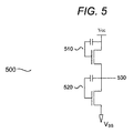
幾つかの実施形態では、OTP及びMTPデバイスが浮遊ゲート上に蓄積された電荷の損失に対する十分な耐性を確実に備えるようにさらなる保護を実行できる。このために、デバイスは図5に示すように、一対のラッチ500内に構成でき、そこでデータ及びその補数が該ラッチ内に保存され、その結果保存されたデータ内におけるマージンを効果的に2倍にする。そこに示されるように、上部デバイス510はノード530を第1電圧基準(Vcc)に結合させるが、第2の下部デバイス520は該ノードを第2電圧基準(Vss)に結合させる。上部デバイス浮遊ゲートに帯電させることによって上部デバイス510は非導電状態にプログラムされ、ノード530は下部デバイス520によってVssに確実に引き下げられ、第1論理データ値(0)を示すこととなる。同様に、下部デバイス浮遊ゲートに帯電させることによって、下部デバイス520は非導電状態にプログラムされ、ノード530は上部デバイス510によってVccに確実に引き上げられ、第2論理データ値(1)を示すこととなる。
In some embodiments, additional protection can be performed to ensure that the OTP and MTP devices are sufficiently resistant to the loss of charge stored on the floating gate. To this end, the device can be configured in a pair of
本発明の好適な実施形態の別の有用な利点は、最も従来型の各単層ポリOTPは、通常PMOSデバイス構造で実行されるが、本実施例はNMOSデバイス構造で実行されることである。これは、デバイスをウエハ上の他の各nチャネルデバイスと同時に形成できることを意味している。本発明におけるNMOSデバイス構造の別の利点は、該デバイスがEPROMデバイスと同じように機能するということであり、すなわち、デバイスは伝導状態から非伝導状態にプログラムされる。対称的に、米国特許公開公報第2008/0186772号の先行技術のタイプのデバイス及び一般に使用される他の各PMOS・OTPデバイスは、非伝導状態から伝導状態にプログラムされる。従って、本発明の本態様は、PMOSデバイスが製造工場から出て非伝導状態になるのを確認するために一般にPMOS・OTPデバイスと関連する追加のマスキングステップの必要性を取り除くことができる。 Another useful advantage of the preferred embodiment of the present invention is that each conventional single layer poly OTP is typically implemented with a PMOS device structure, but this embodiment is implemented with an NMOS device structure. . This means that the device can be formed simultaneously with each other n-channel device on the wafer. Another advantage of the NMOS device structure in the present invention is that it functions in the same way as an EPROM device, i.e., the device is programmed from a conducting state to a non-conducting state. In contrast, the prior art type device of US 2008/0186772 and each other commonly used PMOS OTP device is programmed from a non-conducting state to a conducting state. Thus, this aspect of the present invention can eliminate the need for an additional masking step generally associated with PMOS OTP devices to ensure that the PMOS devices exit the manufacturing plant and become non-conductive.
さらに、チャネル熱電子注入(channel hot electrons injection)を伴うNMOSデバイスのプログラミング機構が自己制御式であるため、チャネル熱電子プログラミングを伴うPMOSの場合とは異なり、本発明におけるプログラミング中のエネルギー消費量は自己制御される。 In addition, because the programming mechanism of the NMOS device with channel hot electron injection is self-regulating, the energy consumption during programming in the present invention is different from the case of PMOS with channel thermionic programming. Self-controlled.
それゆえ、本明細書に示すように、浮遊ゲートの特定の構成は決定的ではない。必要なのは、チャネル伝導を制御するよう構造的及び電気的に構成され、電荷キャリアの電気的ソースに容量的に結合されることだけである。所望のレイアウトまたはマスクに従って、特定の形状に変更可能である。場合によっては、浮遊ゲートを例えば多層構造として実装することが望ましい。さらに、容量結合は使用される各材料の機能であるので、本発明は、浮遊ゲートの構成を要望通り収容するように変更及び特定のプロセスに統合できるように、大幅な柔軟性を認めている。本教示に従って構築された各セルのアレイは、閾値セルを有する各セルが形成できるように異なる形状や大きさの各浮遊ゲートを備えることができる。 Thus, as shown herein, the particular configuration of the floating gate is not critical. All that is required is that it be structurally and electrically configured to control channel conduction and capacitively coupled to an electrical source of charge carriers. It can be changed to a specific shape according to the desired layout or mask. In some cases, it is desirable to mount the floating gate as a multilayer structure, for example. Furthermore, since capacitive coupling is a function of each material used, the present invention allows for great flexibility so that the configuration of the floating gate can be modified and integrated into a specific process to accommodate it as desired. . Each cell array constructed in accordance with the present teachings can include each floating gate of a different shape and size such that each cell having a threshold cell can be formed.
可変結合
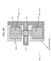
本発明の他の実施形態では、デバイス100の効果的な結合比は、読取り、プログラム及び/又は消去操作の間で異なる、或いは変更することができる。すなわち、図1及び図2には示されていないが、浮遊ゲートに結合されるドレイン領域120は、一つ以上の別々の各サブ領域に分割できる。この詳細を図6A及び6Bに示す。各サブ領域121、122などは、浮遊ゲートとの重複量が異なるように製造又は制御されることが可能である。そのような一つ以上のサブ領域に対して異なる電圧を選択的に印加することによって、読取り/プログラム/消去操作に対して異なる種類の性能が実現可能となる。例えば、超低電力(しかしいくらか遅めの)プログラム又は消去操作があることが望ましい。これは、第2タイプ(読取り)操作中に使用される名目上のエリアよりも小さいそのような第1タイプの操作用の結合エリアを作成することによって実現できる。
Variable Coupling In other embodiments of the present invention, the effective coupling ratio of
図6A及び図6Bにおいて、可変結合ジオメトリは、ドレイン拡散の大きさを(拡散マスクにおいて)変更し、浮遊ゲートの大きさを一定に保つことによって行われるが、同じ実効性のある結果は、ドレイン拡散を一定に保って浮遊ゲートの大きさを変更することによって実現できることは当業者に明らかになるであろう。例えば、浮遊ゲート領域122は、サイズを縮小することによって同じ結果をもたらすことができる。各浮遊ゲートのサイズを調整することによって、各拡散領域を同様に共有することが可能になり、その結果、(他のセル用の)隣接した浮遊ゲート122’は、ドレイン領域120に結合できる。これらの技術の他の組み合わせも同様に使用可能であり、設計/性能要求に基づいて選択可能である。
6A and 6B, the variable coupling geometry is done by changing the drain diffusion size (in the diffusion mask) and keeping the floating gate size constant, but the same effective result is the drain It will be apparent to those skilled in the art that this can be achieved by changing the size of the floating gate while keeping the diffusion constant. For example, the floating
特に、本発明の可変結合の各態様は、PMOS及びNMOSのOTP両方に使用可能である。多状態保存、すなわちマルチレベルのOTPの可能性がある浮遊ゲート上に異なる電圧を与えるよう異なる結合比の選択も利用できる。 In particular, the variable coupling aspects of the present invention can be used for both PMOS and NMOS OTPs. Different coupling ratio selections are also available to provide different voltages on floating gates that are multi-state preserved, ie multi-level OTP potential.
別の実施形態として、当然ながらプログラム供給電圧を代わりに調整することによってドレイン結合が行われ、特定のセルに印加されたプログラム供給電圧は浮遊ゲートに異なる状態を書き込むように調整される。ドレインは浮遊ゲートに結合されるため、可変プログラム供給電圧は浮遊ゲートに供給されるべきである。例えば、ドレイン電圧は、3、4種類以上の異なるレベルを有するように調整できる。これにより異なる形式の可変容量結合をもたらし、該結合は書き込みの観点からはより複雑になるが、幾つかのアプリケーションでは有用となるであろう。 In another embodiment, of course, drain coupling is accomplished by instead adjusting the program supply voltage, and the program supply voltage applied to a particular cell is adjusted to write different states to the floating gate. Since the drain is coupled to the floating gate, the variable program supply voltage should be supplied to the floating gate. For example, the drain voltage can be adjusted to have three, four or more different levels. This results in a different type of variable capacitive coupling, which is more complex from a write perspective, but may be useful in some applications.
NMOS実行用のマルチレベルOTPの変形例は、当該状態を感知するために印加された異なる各ドレイン電圧を通じて異なるレベルの各浮遊ゲート電圧を使用する場合を除いて、NMOSはオフ状態にプログラムされ、多少オフ状態であることは、十分にオフ状態であることと非常に類似していることを考慮に入れなければならない。しかしながら、そのような状況においては、異なるドレイン電圧は読取妨害耐性を不適切に低下させることもあり、ここで交換される可能姓がある。 A variation of the multi-level OTP for NMOS implementation is that the NMOS is programmed to an off state, except when using different levels of each floating gate voltage through different drain voltages applied to sense the state, It must be taken into account that being somewhat off is very similar to being fully off. However, in such a situation, different drain voltages may improperly reduce read disturb tolerance and can be replaced here.
マルチレベル性能の他の選択肢については、異なるドレインからゲートへのキャパシタンス選択がプログラミング状態を選択するのに(異なる重複エリアを通って)使用されるので、読取り操作は、多状態のセルを検出するために同じ単一ドレイン重複によって実行できる。例えば、二つの異なるドレイン重複により、合計2ビットが実行可能である。そのような実行において、ドレイン1は、ドレイン2の結合比の数倍(この場合2の倍数が好ましい)の結合比を有するように設定可能である。 For other choices of multi-level performance, read operations detect multi-state cells because different drain-to-gate capacitance selections are used to select programming states (through different overlapping areas). Can be performed by the same single drain overlap. For example, a total of 2 bits can be implemented due to two different drain overlaps. In such an implementation, drain 1 can be set to have a coupling ratio that is several times the coupling ratio of drain 2 (a multiple of 2 is preferred in this case).
以下の表が示すように、ドレイン1に0Vの電圧及びドレイン2に6Vの電圧を付与するプログラム供給電圧は、ゲートに付与された第1の電荷量に基づいて、セルに第1状態を書き込むことになる。代わりに全てのドレインをプログラムする場合、追加された電荷はさらに高くなり、第2状態などに対応する。 As shown in the following table, a program supply voltage that applies a voltage of 0 V to drain 1 and a voltage of 6 V to drain 2 writes the first state to the cell based on the first charge amount applied to the gate. It will be. If instead all drains are programmed, the added charge will be higher, corresponding to the second state, etc.
合計四つの異なる結合(0(ドレインなし))、1x(ドレイン2)、2x(ドレイン1)、3x(ドレイン1及びドレイン2の両方))が四つの異なる閾値電圧に対応し、それに伴って四つの異なる論理状態がこの単純な配列において達成可能となる。 A total of four different combinations (0 (no drain), 1x (drain 2), 2x (drain 1), 3x (both drain 1 and drain 2)) correspond to four different threshold voltages, Two different logic states can be achieved in this simple array.
以下の表2に示すように、セルの状態を読取る好適な方法は、ドレイン1及びドレイン2の両方に読取り電圧を印加することである。その結果、浮遊ゲート上の電荷量と反比例するセル電流の量が検出される。上述のように、浮遊ゲート上の電荷は、プログラミング中に適用される結合量の一次関数である。従って、セルにおける0、1x、2x及び3xの状態は読取り電流との関係によって検出できる。この実施形態において、読取りドレイン電圧は約1ボルトに選択されることが好ましい。これは、いかなる種類の読取り妨害又はドレインが引き起こす漏洩を防ぐという利点がある。 As shown in Table 2 below, the preferred method of reading the state of the cell is to apply a read voltage to both drain 1 and drain 2. As a result, the amount of cell current that is inversely proportional to the amount of charge on the floating gate is detected. As mentioned above, the charge on the floating gate is a linear function of the amount of coupling applied during programming. Thus, the 0, 1x, 2x and 3x states in the cell can be detected by the relationship with the read current. In this embodiment, the read drain voltage is preferably selected to be about 1 volt. This has the advantage of preventing any kind of read disturb or leakage caused by the drain.
読取り操作中にデコードを少なくする代替案として、読取りは、本実施例において最も高い結合比である2xドレインによってドレインノード上で常に行うことができる。そのような場合、全ての四つの異なる状態間で差別化することは可能ではないが、幾つかのアプリケーションにおいては好適なトレードオフとなるかもしれない。 As an alternative to reducing decoding during the read operation, the read can always be done on the drain node by the 2x drain, which is the highest coupling ratio in this embodiment. In such a case, it is not possible to differentiate between all four different states, but may be a good tradeoff in some applications.
同様に表2に示すように、マルチレベルセル状態を読取るさらなる代替手段として、各ドレインのおのおの(又は組み合わせ)に徐々に電圧を変更しながらバイアスをかけることによって結集した重複部分からの結合電荷寄与(coupled charge contribution)を決定する。閾値電圧が、セルの状態を確認するための特定の電圧レベルで特定の時間間隔内において達成又はデコードされるまで、ドレインに徐々に(0からゲートを最も高い閾値状態にするのに十分な任意の目標電圧にまで)増加する電圧でバイアスをかける。従って、全て又は幾つかのドレインはプログラム操作中にバイアスをかけられるが、単一ドレインだけは(上記のように、他のドレインにもバイアスをかけられるが)セルの状態を決定するために読取り中にバイアスをかけられる必要がある。特定の範囲の読取りドレイン電圧は、望ましい操作特性などの特定のセル構造に左右され、定期的な検査によって決定できる。また、この実施形態においても、全ての四つの異なる状態の間で差別化をすることは可能ではないが、幾つかのアプリケーションにおいては好適なトレードオフとなるかもしれない。セルをプログラミング及び読取るための他の実施例が当業者に明らかになるであろう。 Similarly, as shown in Table 2, as a further alternative to reading the multi-level cell state, the combined charge contributions from overlapping portions assembled by biasing each (or combination) of each drain by gradually changing the voltage Determine (coupled charge contribution). Gradually into the drain (from 0 to any threshold sufficient to bring the gate to the highest threshold state) until the threshold voltage is achieved or decoded within a specific time interval at a specific voltage level to confirm the state of the cell Bias with increasing voltage (to the target voltage). Thus, all or some of the drains can be biased during the program operation, but only a single drain can be read to determine the state of the cell (although other drains can be biased as described above). Need to be biased in. The specific range of read drain voltage depends on the specific cell structure, such as the desired operating characteristics, and can be determined by periodic inspection. Also in this embodiment, it is not possible to differentiate between all four different states, but it may be a good trade-off in some applications. Other embodiments for programming and reading the cell will be apparent to those skilled in the art.
当然ながら、他の結合比も可能であるが、2の倍数でない異なる比率を選択することによる制約を受け、検出マージン/差別化は優れていないかもしれない。しかしながら、場合によっては、それぞれの重複部分を任意のより高い/より低い倍率に設定するのが望ましく、それにより任意の出力範囲で二つの隣接する状態間の検出マージンを減少させる効果を持つであろう。しかしながら、検出範囲の感度が不均等である場合、これが好適な選択肢になるであろう(すなわち、4xと5xとの間よりも1xと2xとの間の差異を検出するほうが容易である場合、又はその逆の場合も同じである)。さらに、場合によっては、奇数の論理状態になる各組み合わせの一つを捨てることによって有効論理状態の数を減少することが望ましい。例えば、マルチビットセルは、単に{0、ドレイン1、ドレイン2}の三つのプログラムされたドレイン結合を有することができ、{ドレイン1+ドレイン2}は無視することとなる。 Of course, other coupling ratios are possible, but the detection margin / differentiation may not be excellent, subject to the constraints of choosing a different ratio that is not a multiple of 2. However, in some cases it may be desirable to set each overlap to an arbitrarily higher / lower magnification, which has the effect of reducing the detection margin between two adjacent states in any output range. Let's go. However, if the sensitivity of the detection range is unequal, this would be a good option (ie if it is easier to detect the difference between 1x and 2x than between 4x and 5x, Or vice versa). Further, in some cases, it may be desirable to reduce the number of valid logic states by discarding one of each combination that results in an odd number of logic states. For example, a multi-bit cell can simply have three programmed drain couplings of {0, drain 1, drain 2} and {drain 1 + drain 2} will be ignored.
二つの別々の結合比を図6Aに示し、三つの別々の結合比を図6Bに示すが、他の分割や結合が本教示に従って実行できることが理解されるであろう。例えば、図6Bの場合、3つの異なるレベルの電荷結合を利用することによって8つの異なるプログラム状態が実現できる。例えば、1x、2x及び4xの結合比を有する各ドレインの異なる組み合わせは統合することが可能であり、又は幾つかの他の比率の組み合わせでもよい。さらに、他の選択は、各状態間のより高いマージンと引き換えに、より少ない各論理状態で行うことができる。本発明の他の変化形が当業者に明らかになるであろう。 Although two separate coupling ratios are shown in FIG. 6A and three separate coupling ratios are shown in FIG. 6B, it will be understood that other splits and combinations can be performed in accordance with the present teachings. For example, in the case of FIG. 6B, eight different programming states can be realized by utilizing three different levels of charge coupling. For example, different combinations of drains having 1x, 2x and 4x coupling ratios can be combined, or some other ratio combination. Furthermore, other selections can be made with fewer logic states at the expense of higher margins between the states. Other variations of the invention will be apparent to those skilled in the art.
上記の説明は、提案された各発明の単なる例示的な各実施形態にすぎない。本発明に与えられた保護は、上記の実施形態とは異なる実施形態を同様に含み、適用されるが、該実施形態は本願請求項の範囲内に入るものであることが理解される。 The above descriptions are merely exemplary embodiments of each proposed invention. The protection afforded this invention includes and applies to embodiments that differ from the above-described embodiments, but it is understood that such embodiments fall within the scope of the claims.
Claims (44)
ソース領域と、
ドレイン領域と、
前記ソース領域と前記ドレイン領域とを結合するnチャネルと
を備え、
前記浮遊ゲートは、前記nチャネルを越えて延在し、前記ドレイン領域のドレイン接合面から延長しているアクティブ領域に重なる重複領域を有しており、
前記ドレイン領域は、前記ドレイン領域に印加されて前記デバイスをプログラムするプログラム供給電圧を、前記浮遊ゲートと前記ドレイン領域との間にある空間的な容量結合によって前記浮遊ゲートに付与できるように前記重複領域において前記ゲートの大部分に重なり、
さらに前記デバイスは、1ビットを超える情報を前記プログラム供給電圧によって保存できるように構成される、基板上に位置するプログラマブル多状態不揮発性デバイス。 A floating gate made of a material located on a substrate and used as a gate for a transistor device associated with at least one logic gate or volatile memory;
A source area,
A drain region;
An n-channel coupling the source region and the drain region;
The floating gate has an overlapping region extending beyond the n-channel and overlapping an active region extending from a drain junction surface of the drain region;
The drain region, the program supply voltage to program the device is applied to the drain region, so that it can be applied to the floating gate by spatial capacitive coupling is between the floating gate and the drain region overlapping Overlaps most of the gate in the region ,
Further, the device is a programmable multi-state non-volatile device located on a substrate configured to store more than one bit of information with the program supply voltage.
ソース領域と、
第1ドレイン領域及び第2ドレイン領域から成るドレイン領域と、
前記ソース領域と前記ドレイン領域とを結合するnチャネルと
を備え、
前記浮遊ゲートは、前記nチャネルを越えて延在し、前記ドレイン領域のドレイン接合面から延長しているアクティブ領域に重なる重複領域を有しており、
前記ドレイン領域は、前記ドレイン領域に印加されて前記デバイスをプログラムするプログラム供給電圧を、前記浮遊ゲートと前記ドレイン領域との間にある空間的な容量結合によって前記浮遊ゲートに付与できるように前記重複領域において前記ゲートの大部分に重なり、
さらに、前記デバイスは、複数ビットのデータが前記プログラム供給電圧によって書き込みできるように構成される、基板上に位置するマルチレベルプログラマブルデバイス。 A floating gate made of a material containing impurities that functions as a charge storage position, and is used as an insulating layer for each other non-programmable device located on the substrate;
A source area,
A drain region comprising a first drain region and a second drain region;
An n-channel coupling the source region and the drain region ;
The floating gate has an overlapping region extending beyond the n-channel and overlapping an active region extending from a drain junction surface of the drain region;
The drain region, the program supply voltage to program the device is applied to the drain region, so that it can be applied to the floating gate by spatial capacitive coupling is between the floating gate and the drain region overlapping Overlaps most of the gate in the region ,
Further, the device is a multi-level programmable device located on a substrate configured such that a plurality of bits of data can be written by the program supply voltage.
ソース領域と、
前記浮遊ゲートの一部分に重なり、少なくとも第1ドレイン領域及び第2選択可能ドレイン領域を有するドレイン領域と、
前記ソース領域と前記ドレイン領域とを結合するnチャネルと
を備え、
前記浮遊ゲートは、前記nチャネルを越えて延在し、前記ドレイン領域のドレイン接合面から延長しているアクティブ領域に重なる重複領域を有しており、
前記ドレイン領域と前記浮遊ゲートとの間にある空間的な可変容量結合は、前記重複領域において前記ドレイン領域と前記浮遊ゲートとの間に該可変容量結合を達成するように前記浮遊ゲートに付与される操作電圧として、前記第1ドレイン領域及び前記第2選択可能ドレイン領域にそれぞれ適用される一つ以上の選択信号によって実現でき、
前記可変容量結合によって、前記第1ドレイン領域及び前記第2選択可能ドレイン領域からの可変量のチャネル熱電子に前記浮遊ゲートの閾値を恒久的に変更させ、OTPデバイス内にマルチビットデータを保存させる、基板上に位置するマルチレベルワンタイムプログラマブル(MOTP)デバイス。 A floating gate located on the substrate and made of material shared by at least one logic gate or transistor device associated with a volatile memory and / or another gate;
A source area,
A drain region overlapping at least a portion of the floating gate and having at least a first drain region and a second selectable drain region ;
An n-channel coupling the source region and the drain region ;
The floating gate has an overlapping region extending beyond the n-channel and overlapping an active region extending from a drain junction surface of the drain region;
Spatial variable capacitive coupling between the drain region and the floating gate is imparted to the floating gate to achieve the variable capacitive coupling between the drain region and the floating gate in the overlap region. The operation voltage can be realized by one or more selection signals respectively applied to the first drain region and the second selectable drain region,
The variable capacitive coupling causes a variable amount of channel thermal electrons from the first drain region and the second selectable drain region to permanently change the threshold value of the floating gate to store multi-bit data in the OTP device. Multi-level one-time programmable (MOTP) device located on the substrate.
前記不純物ソースと前記不純物ドレインとを結合するn型チャネルを備え、
前記ゲートは、前記n型チャネルを越えて延在し、前記不純物ドレインのドレイン接合面から延長しているアクティブ領域に重なる重複領域を有しており、
前記n型不純物ドレインは、前記n型不純物ドレインに印加されて前記デバイスをプログラムする可変プログラム供給電圧を、前記ゲートと前記n型不純物ドレインとの間にある空間的な容量結合によって前記ゲートに付与し、マルチレベル論理状態を前記デバイス内に保存できるように前記重複領域において前記ゲートの大部分に重なり、
前記ゲートは、前記デバイスが前記可変プログラム供給電圧によって前記ゲート上に蓄積された電荷量によって画定されるマルチレベルプログラム状態にあるように浮遊ゲートとしての機能に適応し、
さらに、前記浮遊ゲート上の前記電荷は、前記デバイスが再プログラム可能となるように消去できる、マルチレベルプログラマブルメモリデバイス。 A multi-level programmable memory device having a gate, an n-type impurity source, and an n-type impurity drain on a silicon substrate,
An n-type channel for coupling the impurity source and the impurity drain ;
The gate has an overlapping region extending beyond the n-type channel and overlapping an active region extending from a drain junction surface of the impurity drain;
The n-type impurity drain applies a variable program supply voltage applied to the n-type impurity drain to program the device to the gate by a spatial capacitive coupling between the gate and the n-type impurity drain. And overlapping a majority of the gates in the overlap region so that multi-level logic states can be stored in the device,
The gate adapts to function as a floating gate so that the device is in a multi-level program state defined by the amount of charge stored on the gate by the variable program supply voltage;
Furthermore, the charge on the floating gate can be erased such that the device can be reprogrammed.
前記不純物ソースと前記不純物ドレインとを結合するn型チャネルを備え、
前記ゲートは、前記n型チャネルを越えて延在し、前記不純物ドレインのドレイン接合面から延長しているアクティブ領域に重なる重複領域を有しており、
前記n型不純物ドレインは、前記n型不純物ドレインに印加されて前記セルをプログラムする電圧を空間的な容量結合によって前記ゲートに付与できるように前記重複領域において前記ゲートの可変部分に重なるように構成され、
前記ゲートは、前記MOTPセルが前記ゲートの荷電状態によって画定されるプログラム状態にあるように構成され、前記荷電状態は複数のビットのデータに対応する、マルチレベルワンタイムプログラマブルメモリセル。 A multi-level one-time programmable (MOTP) memory cell having a gate, an n-type impurity source, and an n-type impurity drain on a silicon substrate,
An n-type channel for coupling the impurity source and the impurity drain ;
The gate has an overlapping region extending beyond the n-type channel and overlapping an active region extending from a drain junction surface of the impurity drain;
The n-type impurity drain is configured to overlap a variable portion of the gate in the overlapping region so that a voltage applied to the n-type impurity drain to program the cell can be applied to the gate by spatial capacitive coupling. And
The multi-level one-time programmable memory cell, wherein the gate is configured such that the MOTP cell is in a programmed state defined by a charge state of the gate, the charge state corresponding to a plurality of bits of data.
ソース領域と、
第1ドレイン領域及び少なくとも一つの別の第2ドレイン領域から成るドレイン領域と、
前記ソース領域と前記ドレイン領域とを結合するチャネルと
を備え、
前記浮遊ゲートは、前記チャネルを越えて延在し、前記ドレイン領域のドレイン接合面から延長しているアクティブ領域に重なる重複領域を有しており、
前記ドレイン領域は、前記ドレイン領域に印加されて前記デバイスをプログラムするプログラム供給電圧を、前記浮遊ゲートと前記ドレイン領域との間にある空間的な容量結合によって前記浮遊ゲートに付与できるように前記重複領域において前記ゲートの大部分に重なり、
さらに、前記デバイスは、前記第1ドレイン領域及び前記第2ドレイン領域のうち複数の異なる領域がプログラム及び読取り作業中にそれぞれ前記ゲートに結合できるように構成される、基板上に位置するプログラマブル不揮発性デバイス。 A floating gate made of a material located on a substrate and used as a gate for a transistor device associated with at least one logic gate or volatile memory;
A source area,
A drain region comprising a first drain region and at least one other second drain region ;
A channel for coupling the source region and the drain region ;
The floating gate has an overlapping region extending beyond the channel and overlapping an active region extending from a drain junction surface of the drain region;
The drain region, the program supply voltage to program the device is applied to the drain region, so that it can be applied to the floating gate by spatial capacitive coupling is between the floating gate and the drain region overlapping Overlaps most of the gate in the region ,
Further, the device is a programmable non-volatile located on a substrate configured such that a plurality of different regions of the first drain region and the second drain region can be coupled to the gate, respectively, during programming and reading operations. device.
ソース領域と、
ドレイン領域と
前記ソース領域と前記ドレイン領域とを結合するnチャネルと
を備え、
前記浮遊ゲートは、前記nチャネルを越えて延在し、前記ドレイン領域のドレイン接合面から延長しているアクティブ領域に重なる重複領域を有しており、
前記ドレイン領域は、前記ドレイン領域に印加されて前記デバイスをプログラムするプログラム供給電圧を、前記浮遊ゲートと前記ドレイン領域との間にある空間的な容量結合によって前記浮遊ゲートに付与できるように前記重複領域において前記ゲートの大部分に重なり、
さらに、前記デバイスは、プログラマブルデバイス用の可変閾値をもたらすためのプログラム操作中に、可変プログラム供給電圧を前記ゲートに結合できるように構成される、基板上に位置するプログラマブルデバイス。 A floating gate made of a material containing impurities that functions as a charge storage position, and is used as an insulating layer for each other non-programmable device located on the substrate;
A source area,
Drain region and
An n-channel coupling the source region and the drain region ;
The floating gate has an overlapping region extending beyond the n-channel and overlapping an active region extending from a drain junction surface of the drain region;
The drain region, the program supply voltage to program the device is applied to the drain region, so that it can be applied to the floating gate by spatial capacitive coupling is between the floating gate and the drain region overlapping Overlaps most of the gate in the region ,
Further, the device is a programmable device located on a substrate configured to allow a variable program supply voltage to be coupled to the gate during a program operation to provide a variable threshold for the programmable device.
基板上に位置し、少なくとも一つの論理ゲート又は揮発性メモリと関連するトランジスタデバイス用の相互接続ゲート及び/又は別のゲートが共用する材料から成る浮遊ゲートと、
ソース領域と、
前記浮遊ゲートの一部分に重なり、少なくとも第1ドレイン領域と第2選択可能ドレイン領域とを有するドレイン領域と
前記ソース領域と前記ドレイン領域とを結合するnチャネルと
を備え、
前記浮遊ゲートは、前記nチャネルを越えて延在し、前記ドレイン領域のドレイン接合面から延長しているアクティブ領域に重なる重複領域を有しており、
前記ドレイン領域と前記浮遊ゲートとの間にある空間的な可変容量結合は、前記重複領域において前記ドレイン領域と前記浮遊ゲートとの間に該可変容量結合を達成するように前記浮遊ゲートに付与されるプログラム電圧として、前記第1ドレイン領域と前記第2選択可能ドレイン領域とにそれぞれ適用される一つ以上の選択信号によって実現可能であり、
前記可変容量結合によって、前記第1ドレイン領域と前記第2選択可能ドレイン領域から可変量のチャネル熱電子が、前記浮遊ゲートの閾値を恒久的に変更し、前記OTPデバイスにデータを保存する、基板上に位置するワンタイムプログラマブル(OTP)デバイス。 One time programmable (OTP) device,
A floating gate located on the substrate and made of material shared by at least one logic gate or transistor device associated with a volatile memory and / or another gate;
A source area,
A drain region overlapping at least a portion of the floating gate and having at least a first drain region and a second selectable drain region;
An n-channel coupling the source region and the drain region ;
The floating gate has an overlapping region extending beyond the n-channel and overlapping an active region extending from a drain junction surface of the drain region;
Spatial variable capacitive coupling between the drain region and the floating gate is imparted to the floating gate to achieve the variable capacitive coupling between the drain region and the floating gate in the overlap region. Can be realized by one or more selection signals applied to the first drain region and the second selectable drain region, respectively.
A substrate with a variable amount of channel thermoelectrons from the first drain region and the second selectable drain region that permanently changes a threshold value of the floating gate and stores data in the OTP device due to the variable capacitive coupling. One time programmable (OTP) device located above.
a.浮遊ゲートに空間的に容量的に結合されるドレイン領域と、ソース領域と前記ドレイン領域とを結合するnチャネルとを有し、前記浮遊ゲートは、前記nチャネルを越えて延在し、前記ドレイン領域のドレイン接合面から延長しているアクティブ領域に重なる重複領域を有しており、
b.前記OTPメモリデバイスの任意及びすべての領域と各構造とは、前記少なくとも一つの他の追加論理デバイス又は非OTPメモリデバイスの各構成要素として使用される各対応領域及び構造から単に由来し、
c.前記浮遊ゲートと前記ドレイン領域との間にある空間的な容量結合の量は、前記重複領域において前記ドレイン領域と前記浮遊ゲートとの間に該可変容量結合を達成するように、前記ドレイン領域に付与されて前記浮遊ゲートに付与される操作電圧によって、少なくとも一つの異なるプログラム、消去、又は読取りの操作中に変化させることができることを特徴とするメモリデバイス。 A one-time programmable (OTP) memory device incorporated on a silicon substrate with at least one other additional logic device or non-OTP memory device,
a. A drain region spatially capacitively coupled to the floating gate ; and an n-channel coupling the source region and the drain region , wherein the floating gate extends beyond the n-channel and the drain It has an overlapping region that overlaps the active region extending from the drain junction surface of the region,
b. Any and all regions and structures of the OTP memory device are simply derived from the corresponding regions and structures used as components of the at least one other additional logical device or non-OTP memory device,
c. The amount of spatial capacitive coupling between the floating gate and the drain region is such that the variable capacitance coupling is achieved in the drain region so as to achieve the variable capacitive coupling between the drain region and the floating gate in the overlapping region. A memory device characterized in that it can be varied during at least one different program, erase, or read operation by an applied voltage applied to the floating gate.
a.浮遊ゲートに空間的に容量的に結合されるドレイン領域と、ソース領域と前記ドレイン領域とを結合するnチャネルとを有し、前記浮遊ゲートは、前記nチャネルを越えて延在し、前記ドレイン領域のドレイン接合面から延長しているアクティブ領域に重なる重複領域を有しており、
b.前記MOTPメモリセルの任意及びすべての領域と各構造は、前記少なくとも一つの他の追加論理デバイス又は非MOTPメモリデバイスの各構成要素として使用される各対応領域及び構造から単に由来し、
c.前記浮遊ゲートと前記ドレイン領域との間にある空間的な容量結合の量は、前記重複領域において前記ドレイン領域と前記浮遊ゲートとの間に該可変容量結合を達成するように前記浮遊ゲートに付与される、単一MOTPメモリセル内に複数ビットのデータを保存するためのプログラム操作中に印加された電圧によって変更できることを特徴とするメモリセル。 A multi-level one-time programmable (MOTP) memory cell incorporated on a silicon substrate with at least one other additional logic device and / or non-OTP memory device,
a. A drain region spatially capacitively coupled to the floating gate ; and an n-channel coupling the source region and the drain region , wherein the floating gate extends beyond the n-channel and the drain It has an overlapping region that overlaps the active region extending from the drain junction surface of the region,
b. Any and all regions and structures of the MOTP memory cell are simply derived from corresponding regions and structures used as components of the at least one other additional logic device or non-MOTP memory device,
c. The amount of spatial capacitive coupling between the floating gate and the drain region is applied to the floating gate so as to achieve the variable capacitive coupling between the drain region and the floating gate in the overlapping region. The memory cell can be changed according to a voltage applied during a program operation for storing a plurality of bits of data in a single MOTP memory cell.
Applications Claiming Priority (17)
| Application Number | Priority Date | Filing Date | Title |
|---|---|---|---|
| US98786907P | 2007-11-14 | 2007-11-14 | |
| US60/987,869 | 2007-11-14 | ||
| US12/264,076 US7787309B2 (en) | 2007-11-01 | 2008-11-03 | Method of operating integrated circuit embedded with non-volatile one-time-programmable and multiple-time programmable memory |
| US12/264,060 US7787304B2 (en) | 2007-11-01 | 2008-11-03 | Method of making integrated circuit embedded with non-volatile one-time-programmable and multiple-time programmable memory |
| US12/264,076 | 2008-11-03 | ||
| US12/264,029 | 2008-11-03 | ||
| US12/264,060 | 2008-11-03 | ||
| US12/264,029 US7782668B2 (en) | 2007-11-01 | 2008-11-03 | Integrated circuit embedded with non-volatile one-time-programmable and multiple-time programmable memory |
| US12/271,695 US7787295B2 (en) | 2007-11-14 | 2008-11-14 | Integrated circuit embedded with non-volatile multiple-time programmable memory having variable coupling |
| US12/271,695 | 2008-11-14 | ||
| US12/271,666 US8580622B2 (en) | 2007-11-14 | 2008-11-14 | Method of making integrated circuit embedded with non-volatile programmable memory having variable coupling |
| US12/271,647 US7852672B2 (en) | 2007-11-14 | 2008-11-14 | Integrated circuit embedded with non-volatile programmable memory having variable coupling |
| US12/271,666 | 2008-11-14 | ||
| US12/271,680 | 2008-11-14 | ||
| US12/271,647 | 2008-11-14 | ||
| US12/271,680 US7876615B2 (en) | 2007-11-14 | 2008-11-14 | Method of operating integrated circuit embedded with non-volatile programmable memory having variable coupling related application data |
| PCT/US2008/083697 WO2009065084A1 (en) | 2007-11-14 | 2008-11-14 | Integrated circuit embedded with non-volatile programmable memory having variable coupling |
Publications (3)
| Publication Number | Publication Date |
|---|---|
| JP2011503905A JP2011503905A (en) | 2011-01-27 |
| JP2011503905A5 JP2011503905A5 (en) | 2012-03-08 |
| JP5554714B2 true JP5554714B2 (en) | 2014-07-23 |
Family
ID=40639188
Family Applications (1)
| Application Number | Title | Priority Date | Filing Date |
|---|---|---|---|
| JP2010534250A Expired - Fee Related JP5554714B2 (en) | 2007-11-14 | 2008-11-14 | Integrated circuit incorporated in non-volatile programmable memory with variable coupling |
Country Status (2)
| Country | Link |
|---|---|
| JP (1) | JP5554714B2 (en) |
| WO (1) | WO2009065084A1 (en) |
Families Citing this family (2)
| Publication number | Priority date | Publication date | Assignee | Title |
|---|---|---|---|---|
| US9230814B2 (en) * | 2011-10-28 | 2016-01-05 | Invensas Corporation | Non-volatile memory devices having vertical drain to gate capacitive coupling |
| US8975685B2 (en) * | 2012-08-31 | 2015-03-10 | Maxim Integrated Products, Inc. | N-channel multi-time programmable memory devices |
Family Cites Families (14)
| Publication number | Priority date | Publication date | Assignee | Title |
|---|---|---|---|---|
| JPH0521809A (en) * | 1991-07-15 | 1993-01-29 | Matsushita Electric Works Ltd | Semiconductor device |
| US6965142B2 (en) * | 1995-03-07 | 2005-11-15 | Impinj, Inc. | Floating-gate semiconductor structures |
| US5598367A (en) * | 1995-06-07 | 1997-01-28 | International Business Machines Corporation | Trench EPROM |
| US6177703B1 (en) * | 1999-05-28 | 2001-01-23 | Vlsi Technology, Inc. | Method and apparatus for producing a single polysilicon flash EEPROM having a select transistor and a floating gate transistor |
| JP2001358313A (en) * | 2000-06-14 | 2001-12-26 | Hitachi Ltd | Semiconductor device |
| JP4170604B2 (en) * | 2001-04-18 | 2008-10-22 | 株式会社東芝 | Nonvolatile semiconductor memory |
| JP2003197765A (en) * | 2001-12-28 | 2003-07-11 | Texas Instr Japan Ltd | Semiconductor device and its manufacturing method |
| JP4557950B2 (en) * | 2002-05-10 | 2010-10-06 | 株式会社東芝 | Nonvolatile semiconductor memory device |
| US7064978B2 (en) * | 2002-07-05 | 2006-06-20 | Aplus Flash Technology, Inc. | Monolithic, combo nonvolatile memory allowing byte, page and block write with no disturb and divided-well in the cell array using a unified cell structure and technology with a new scheme of decoder and layout |
| AU2003255254A1 (en) * | 2002-08-08 | 2004-02-25 | Glenn J. Leedy | Vertical system integration |
| US6920067B2 (en) * | 2002-12-25 | 2005-07-19 | Ememory Technology Inc. | Integrated circuit embedded with single-poly non-volatile memory |
| JP2005038894A (en) * | 2003-07-15 | 2005-02-10 | Sony Corp | Nonvolatile semiconductor memory apparatus and its operating method |
| JP2005057106A (en) * | 2003-08-06 | 2005-03-03 | Sony Corp | Non volatile semiconductor memory device and its charge injecting method |
| TWI231039B (en) * | 2004-04-30 | 2005-04-11 | Yield Microelectronics Corp | Non-volatile memory and its operational method |
-
2008
- 2008-11-14 WO PCT/US2008/083697 patent/WO2009065084A1/en active Application Filing
- 2008-11-14 JP JP2010534250A patent/JP5554714B2/en not_active Expired - Fee Related
Also Published As
| Publication number | Publication date |
|---|---|
| WO2009065084A1 (en) | 2009-05-22 |
| JP2011503905A (en) | 2011-01-27 |
Similar Documents
| Publication | Publication Date | Title |
|---|---|---|
| JP5581215B2 (en) | Integrated circuits embedded in non-volatile one-time programmable and multi-time programmable memories | |
| US8599612B2 (en) | Method of operating integrated circuit embedded with non-volatile programmable memory having variable coupling related application data | |
| US8705263B2 (en) | Non-volatile one-time-programmable and multiple-time programmable memory configuration circuit | |
| US8208299B2 (en) | Integrated circuit embedded with non-volatile programmable memory having variable coupling and separate read/write paths | |
| US7852672B2 (en) | Integrated circuit embedded with non-volatile programmable memory having variable coupling | |
| US7544569B2 (en) | Bidirectional split gate NAND flash memory structure and array, method of programming, erasing and reading thereof, and method of manufacturing | |
| US6788576B2 (en) | Complementary non-volatile memory cell | |
| JP2009540545A (en) | Nonvolatile memory embedded in a conventional logic process and method of operating such a nonvolatile memory | |
| US8305805B2 (en) | Common drain non-volatile multiple-time programmable memory | |
| US9224739B2 (en) | Method of making integrated circuit embedded with non-volatile programmable memory having variable coupling | |
| US6653682B1 (en) | Non-volatile electrically alterable semiconductor memory device | |
| US6329687B1 (en) | Two bit flash cell with two floating gate regions | |
| JP5554714B2 (en) | Integrated circuit incorporated in non-volatile programmable memory with variable coupling | |
| EP1308962B1 (en) | Single poly embedded EPROM |
Legal Events
| Date | Code | Title | Description |
|---|---|---|---|
| A711 | Notification of change in applicant |
Free format text: JAPANESE INTERMEDIATE CODE: A711 Effective date: 20110516 |
|
| A621 | Written request for application examination |
Free format text: JAPANESE INTERMEDIATE CODE: A621 Effective date: 20111104 |
|
| RD03 | Notification of appointment of power of attorney |
Free format text: JAPANESE INTERMEDIATE CODE: A7423 Effective date: 20111205 |
|
| RD04 | Notification of resignation of power of attorney |
Free format text: JAPANESE INTERMEDIATE CODE: A7424 Effective date: 20111209 |
|
| A521 | Request for written amendment filed |
Free format text: JAPANESE INTERMEDIATE CODE: A523 Effective date: 20120120 |
|
| A131 | Notification of reasons for refusal |
Free format text: JAPANESE INTERMEDIATE CODE: A131 Effective date: 20130813 |
|
| A977 | Report on retrieval |
Free format text: JAPANESE INTERMEDIATE CODE: A971007 Effective date: 20130815 |
|
| A601 | Written request for extension of time |
Free format text: JAPANESE INTERMEDIATE CODE: A601 Effective date: 20131107 |
|
| A602 | Written permission of extension of time |
Free format text: JAPANESE INTERMEDIATE CODE: A602 Effective date: 20131114 |
|
| A521 | Request for written amendment filed |
Free format text: JAPANESE INTERMEDIATE CODE: A523 Effective date: 20131205 |
|
| A131 | Notification of reasons for refusal |
Free format text: JAPANESE INTERMEDIATE CODE: A131 Effective date: 20140207 |
|
| A521 | Request for written amendment filed |
Free format text: JAPANESE INTERMEDIATE CODE: A523 Effective date: 20140407 |
|
| TRDD | Decision of grant or rejection written | ||
| A01 | Written decision to grant a patent or to grant a registration (utility model) |
Free format text: JAPANESE INTERMEDIATE CODE: A01 Effective date: 20140430 |
|
| A61 | First payment of annual fees (during grant procedure) |
Free format text: JAPANESE INTERMEDIATE CODE: A61 Effective date: 20140529 |
|
| R150 | Certificate of patent or registration of utility model |
Ref document number: 5554714 Country of ref document: JP Free format text: JAPANESE INTERMEDIATE CODE: R150 |
|
| R250 | Receipt of annual fees |
Free format text: JAPANESE INTERMEDIATE CODE: R250 |
|
| R250 | Receipt of annual fees |
Free format text: JAPANESE INTERMEDIATE CODE: R250 |
|
| LAPS | Cancellation because of no payment of annual fees |