JP5548356B2 - Method for manufacturing semiconductor device - Google Patents
Method for manufacturing semiconductor device Download PDFInfo
- Publication number
- JP5548356B2 JP5548356B2 JP2008280708A JP2008280708A JP5548356B2 JP 5548356 B2 JP5548356 B2 JP 5548356B2 JP 2008280708 A JP2008280708 A JP 2008280708A JP 2008280708 A JP2008280708 A JP 2008280708A JP 5548356 B2 JP5548356 B2 JP 5548356B2
- Authority
- JP
- Japan
- Prior art keywords
- layer
- semiconductor
- substrate
- region
- single crystal
- Prior art date
- Legal status (The legal status is an assumption and is not a legal conclusion. Google has not performed a legal analysis and makes no representation as to the accuracy of the status listed.)
- Expired - Fee Related
Links
- 239000004065 semiconductor Substances 0.000 title claims description 495
- 238000000034 method Methods 0.000 title claims description 98
- 238000004519 manufacturing process Methods 0.000 title claims description 29
- 239000000758 substrate Substances 0.000 claims description 282
- 239000013078 crystal Substances 0.000 claims description 105
- 150000002500 ions Chemical class 0.000 claims description 97
- 229910052581 Si3N4 Inorganic materials 0.000 claims description 51
- HQVNEWCFYHHQES-UHFFFAOYSA-N silicon nitride Chemical compound N12[Si]34N5[Si]62N3[Si]51N64 HQVNEWCFYHHQES-UHFFFAOYSA-N 0.000 claims description 51
- 229910052710 silicon Inorganic materials 0.000 claims description 42
- 239000010703 silicon Substances 0.000 claims description 42
- XUIMIQQOPSSXEZ-UHFFFAOYSA-N Silicon Chemical compound [Si] XUIMIQQOPSSXEZ-UHFFFAOYSA-N 0.000 claims description 41
- 238000010438 heat treatment Methods 0.000 claims description 37
- 238000005530 etching Methods 0.000 claims description 35
- 230000008569 process Effects 0.000 claims description 32
- VYPSYNLAJGMNEJ-UHFFFAOYSA-N Silicium dioxide Chemical compound O=[Si]=O VYPSYNLAJGMNEJ-UHFFFAOYSA-N 0.000 claims description 31
- 229910052814 silicon oxide Inorganic materials 0.000 claims description 30
- 230000001678 irradiating effect Effects 0.000 claims description 10
- 238000005229 chemical vapour deposition Methods 0.000 claims description 7
- 150000001282 organosilanes Chemical class 0.000 claims description 4
- 241000287463 Phalacrocorax Species 0.000 claims 1
- 239000010410 layer Substances 0.000 description 569
- 239000012535 impurity Substances 0.000 description 144
- 239000010408 film Substances 0.000 description 107
- 239000002585 base Substances 0.000 description 72
- 239000007789 gas Substances 0.000 description 68
- 239000000463 material Substances 0.000 description 45
- 238000006243 chemical reaction Methods 0.000 description 35
- 241000894007 species Species 0.000 description 35
- 239000001257 hydrogen Substances 0.000 description 32
- 229910052739 hydrogen Inorganic materials 0.000 description 32
- UFHFLCQGNIYNRP-UHFFFAOYSA-N Hydrogen Chemical compound [H][H] UFHFLCQGNIYNRP-UHFFFAOYSA-N 0.000 description 31
- 230000006870 function Effects 0.000 description 25
- 230000007547 defect Effects 0.000 description 23
- 229910052782 aluminium Inorganic materials 0.000 description 22
- XAGFODPZIPBFFR-UHFFFAOYSA-N aluminium Chemical compound [Al] XAGFODPZIPBFFR-UHFFFAOYSA-N 0.000 description 22
- 239000010409 thin film Substances 0.000 description 22
- IJGRMHOSHXDMSA-UHFFFAOYSA-N Atomic nitrogen Chemical compound N#N IJGRMHOSHXDMSA-UHFFFAOYSA-N 0.000 description 21
- PXHVJJICTQNCMI-UHFFFAOYSA-N Nickel Chemical compound [Ni] PXHVJJICTQNCMI-UHFFFAOYSA-N 0.000 description 20
- 239000011521 glass Substances 0.000 description 20
- 229910052760 oxygen Inorganic materials 0.000 description 20
- 239000001301 oxygen Substances 0.000 description 20
- 239000010936 titanium Substances 0.000 description 20
- 238000000059 patterning Methods 0.000 description 19
- GPRLSGONYQIRFK-UHFFFAOYSA-N hydron Chemical compound [H+] GPRLSGONYQIRFK-UHFFFAOYSA-N 0.000 description 18
- 230000015572 biosynthetic process Effects 0.000 description 17
- 230000004888 barrier function Effects 0.000 description 16
- QVGXLLKOCUKJST-UHFFFAOYSA-N atomic oxygen Chemical compound [O] QVGXLLKOCUKJST-UHFFFAOYSA-N 0.000 description 15
- 229910052719 titanium Inorganic materials 0.000 description 15
- RTAQQCXQSZGOHL-UHFFFAOYSA-N Titanium Chemical compound [Ti] RTAQQCXQSZGOHL-UHFFFAOYSA-N 0.000 description 14
- 229910052751 metal Inorganic materials 0.000 description 14
- 239000002184 metal Substances 0.000 description 14
- PMHQVHHXPFUNSP-UHFFFAOYSA-M copper(1+);methylsulfanylmethane;bromide Chemical compound Br[Cu].CSC PMHQVHHXPFUNSP-UHFFFAOYSA-M 0.000 description 13
- 230000005684 electric field Effects 0.000 description 13
- 239000004973 liquid crystal related substance Substances 0.000 description 13
- 229910021421 monocrystalline silicon Inorganic materials 0.000 description 13
- 238000005268 plasma chemical vapour deposition Methods 0.000 description 13
- 238000004364 calculation method Methods 0.000 description 12
- 239000010949 copper Substances 0.000 description 12
- BASFCYQUMIYNBI-UHFFFAOYSA-N platinum Chemical compound [Pt] BASFCYQUMIYNBI-UHFFFAOYSA-N 0.000 description 12
- 239000000203 mixture Substances 0.000 description 11
- 229910052750 molybdenum Inorganic materials 0.000 description 11
- 239000011733 molybdenum Substances 0.000 description 11
- 238000012545 processing Methods 0.000 description 11
- 229920005989 resin Polymers 0.000 description 11
- 239000011347 resin Substances 0.000 description 11
- 230000008646 thermal stress Effects 0.000 description 11
- ZOKXTWBITQBERF-UHFFFAOYSA-N Molybdenum Chemical compound [Mo] ZOKXTWBITQBERF-UHFFFAOYSA-N 0.000 description 10
- 230000001133 acceleration Effects 0.000 description 10
- 229910052802 copper Inorganic materials 0.000 description 10
- 229910052757 nitrogen Inorganic materials 0.000 description 10
- 238000000926 separation method Methods 0.000 description 10
- RYGMFSIKBFXOCR-UHFFFAOYSA-N Copper Chemical compound [Cu] RYGMFSIKBFXOCR-UHFFFAOYSA-N 0.000 description 9
- OAICVXFJPJFONN-UHFFFAOYSA-N Phosphorus Chemical compound [P] OAICVXFJPJFONN-UHFFFAOYSA-N 0.000 description 9
- 239000000956 alloy Substances 0.000 description 9
- CSDREXVUYHZDNP-UHFFFAOYSA-N alumanylidynesilicon Chemical compound [Al].[Si] CSDREXVUYHZDNP-UHFFFAOYSA-N 0.000 description 9
- 239000012298 atmosphere Substances 0.000 description 9
- 239000000460 chlorine Substances 0.000 description 9
- 230000000694 effects Effects 0.000 description 9
- 238000010884 ion-beam technique Methods 0.000 description 9
- 229910052759 nickel Inorganic materials 0.000 description 9
- -1 oxygen ions Chemical class 0.000 description 9
- 239000002245 particle Substances 0.000 description 9
- 229910052698 phosphorus Inorganic materials 0.000 description 9
- 239000011574 phosphorus Substances 0.000 description 9
- 239000002356 single layer Substances 0.000 description 9
- XKRFYHLGVUSROY-UHFFFAOYSA-N Argon Chemical compound [Ar] XKRFYHLGVUSROY-UHFFFAOYSA-N 0.000 description 8
- ZOXJGFHDIHLPTG-UHFFFAOYSA-N Boron Chemical compound [B] ZOXJGFHDIHLPTG-UHFFFAOYSA-N 0.000 description 8
- 229910052796 boron Inorganic materials 0.000 description 8
- 229920001940 conductive polymer Polymers 0.000 description 8
- KPUWHANPEXNPJT-UHFFFAOYSA-N disiloxane Chemical class [SiH3]O[SiH3] KPUWHANPEXNPJT-UHFFFAOYSA-N 0.000 description 8
- 230000002093 peripheral effect Effects 0.000 description 8
- 238000009832 plasma treatment Methods 0.000 description 8
- 238000004544 sputter deposition Methods 0.000 description 8
- WFKWXMTUELFFGS-UHFFFAOYSA-N tungsten Chemical compound [W] WFKWXMTUELFFGS-UHFFFAOYSA-N 0.000 description 8
- 229910052721 tungsten Inorganic materials 0.000 description 8
- 239000010937 tungsten Substances 0.000 description 8
- GQPLMRYTRLFLPF-UHFFFAOYSA-N Nitrous Oxide Chemical compound [O-][N+]#N GQPLMRYTRLFLPF-UHFFFAOYSA-N 0.000 description 7
- 239000011651 chromium Substances 0.000 description 7
- 150000001875 compounds Chemical class 0.000 description 7
- 238000001312 dry etching Methods 0.000 description 7
- AMGQUBHHOARCQH-UHFFFAOYSA-N indium;oxotin Chemical compound [In].[Sn]=O AMGQUBHHOARCQH-UHFFFAOYSA-N 0.000 description 7
- 150000004767 nitrides Chemical class 0.000 description 7
- 238000007789 sealing Methods 0.000 description 7
- 229910052715 tantalum Inorganic materials 0.000 description 7
- GUVRBAGPIYLISA-UHFFFAOYSA-N tantalum atom Chemical compound [Ta] GUVRBAGPIYLISA-UHFFFAOYSA-N 0.000 description 7
- OKTJSMMVPCPJKN-UHFFFAOYSA-N Carbon Chemical compound [C] OKTJSMMVPCPJKN-UHFFFAOYSA-N 0.000 description 6
- NRTOMJZYCJJWKI-UHFFFAOYSA-N Titanium nitride Chemical compound [Ti]#N NRTOMJZYCJJWKI-UHFFFAOYSA-N 0.000 description 6
- 229910045601 alloy Inorganic materials 0.000 description 6
- 125000004429 atom Chemical group 0.000 description 6
- 229910052799 carbon Inorganic materials 0.000 description 6
- 239000004020 conductor Substances 0.000 description 6
- 229910003437 indium oxide Inorganic materials 0.000 description 6
- PJXISJQVUVHSOJ-UHFFFAOYSA-N indium(iii) oxide Chemical compound [O-2].[O-2].[O-2].[In+3].[In+3] PJXISJQVUVHSOJ-UHFFFAOYSA-N 0.000 description 6
- 238000009616 inductively coupled plasma Methods 0.000 description 6
- 239000011810 insulating material Substances 0.000 description 6
- 238000005468 ion implantation Methods 0.000 description 6
- 238000004949 mass spectrometry Methods 0.000 description 6
- 230000008018 melting Effects 0.000 description 6
- 238000002844 melting Methods 0.000 description 6
- TWNQGVIAIRXVLR-UHFFFAOYSA-N oxo(oxoalumanyloxy)alumane Chemical compound O=[Al]O[Al]=O TWNQGVIAIRXVLR-UHFFFAOYSA-N 0.000 description 6
- 229910021332 silicide Inorganic materials 0.000 description 6
- FVBUAEGBCNSCDD-UHFFFAOYSA-N silicide(4-) Chemical compound [Si-4] FVBUAEGBCNSCDD-UHFFFAOYSA-N 0.000 description 6
- 239000000126 substance Substances 0.000 description 6
- 238000001039 wet etching Methods 0.000 description 6
- VYZAMTAEIAYCRO-UHFFFAOYSA-N Chromium Chemical compound [Cr] VYZAMTAEIAYCRO-UHFFFAOYSA-N 0.000 description 5
- YCKRFDGAMUMZLT-UHFFFAOYSA-N Fluorine atom Chemical compound [F] YCKRFDGAMUMZLT-UHFFFAOYSA-N 0.000 description 5
- 239000004642 Polyimide Substances 0.000 description 5
- BLRPTPMANUNPDV-UHFFFAOYSA-N Silane Chemical compound [SiH4] BLRPTPMANUNPDV-UHFFFAOYSA-N 0.000 description 5
- 229910052786 argon Inorganic materials 0.000 description 5
- 239000003990 capacitor Substances 0.000 description 5
- 229910052804 chromium Inorganic materials 0.000 description 5
- 230000007423 decrease Effects 0.000 description 5
- 229910052731 fluorine Inorganic materials 0.000 description 5
- 239000011737 fluorine Substances 0.000 description 5
- 229910052732 germanium Inorganic materials 0.000 description 5
- GNPVGFCGXDBREM-UHFFFAOYSA-N germanium atom Chemical compound [Ge] GNPVGFCGXDBREM-UHFFFAOYSA-N 0.000 description 5
- 239000010931 gold Substances 0.000 description 5
- 229910052734 helium Inorganic materials 0.000 description 5
- 230000006872 improvement Effects 0.000 description 5
- 230000007246 mechanism Effects 0.000 description 5
- 230000003647 oxidation Effects 0.000 description 5
- 238000007254 oxidation reaction Methods 0.000 description 5
- 229910052697 platinum Inorganic materials 0.000 description 5
- 229920001721 polyimide Polymers 0.000 description 5
- 238000004151 rapid thermal annealing Methods 0.000 description 5
- 229910000077 silane Inorganic materials 0.000 description 5
- 230000035882 stress Effects 0.000 description 5
- ZAMOUSCENKQFHK-UHFFFAOYSA-N Chlorine atom Chemical compound [Cl] ZAMOUSCENKQFHK-UHFFFAOYSA-N 0.000 description 4
- XEEYBQQBJWHFJM-UHFFFAOYSA-N Iron Chemical compound [Fe] XEEYBQQBJWHFJM-UHFFFAOYSA-N 0.000 description 4
- FYYHWMGAXLPEAU-UHFFFAOYSA-N Magnesium Chemical compound [Mg] FYYHWMGAXLPEAU-UHFFFAOYSA-N 0.000 description 4
- 229910052779 Neodymium Inorganic materials 0.000 description 4
- BQCADISMDOOEFD-UHFFFAOYSA-N Silver Chemical compound [Ag] BQCADISMDOOEFD-UHFFFAOYSA-N 0.000 description 4
- GWEVSGVZZGPLCZ-UHFFFAOYSA-N Titan oxide Chemical compound O=[Ti]=O GWEVSGVZZGPLCZ-UHFFFAOYSA-N 0.000 description 4
- XLOMVQKBTHCTTD-UHFFFAOYSA-N Zinc monoxide Chemical compound [Zn]=O XLOMVQKBTHCTTD-UHFFFAOYSA-N 0.000 description 4
- 229910052783 alkali metal Inorganic materials 0.000 description 4
- 150000001340 alkali metals Chemical class 0.000 description 4
- 229910052784 alkaline earth metal Inorganic materials 0.000 description 4
- 150000001342 alkaline earth metals Chemical class 0.000 description 4
- 229910052801 chlorine Inorganic materials 0.000 description 4
- 239000010941 cobalt Substances 0.000 description 4
- 229910017052 cobalt Inorganic materials 0.000 description 4
- GUTLYIVDDKVIGB-UHFFFAOYSA-N cobalt atom Chemical compound [Co] GUTLYIVDDKVIGB-UHFFFAOYSA-N 0.000 description 4
- 238000004891 communication Methods 0.000 description 4
- 238000010586 diagram Methods 0.000 description 4
- PCHJSUWPFVWCPO-UHFFFAOYSA-N gold Chemical compound [Au] PCHJSUWPFVWCPO-UHFFFAOYSA-N 0.000 description 4
- 229910052737 gold Inorganic materials 0.000 description 4
- 239000001307 helium Substances 0.000 description 4
- SWQJXJOGLNCZEY-UHFFFAOYSA-N helium atom Chemical compound [He] SWQJXJOGLNCZEY-UHFFFAOYSA-N 0.000 description 4
- 125000004435 hydrogen atom Chemical group [H]* 0.000 description 4
- 239000011777 magnesium Substances 0.000 description 4
- 229910052749 magnesium Inorganic materials 0.000 description 4
- 238000007726 management method Methods 0.000 description 4
- QEFYFXOXNSNQGX-UHFFFAOYSA-N neodymium atom Chemical compound [Nd] QEFYFXOXNSNQGX-UHFFFAOYSA-N 0.000 description 4
- 239000010955 niobium Substances 0.000 description 4
- QGLKJKCYBOYXKC-UHFFFAOYSA-N nonaoxidotritungsten Chemical compound O=[W]1(=O)O[W](=O)(=O)O[W](=O)(=O)O1 QGLKJKCYBOYXKC-UHFFFAOYSA-N 0.000 description 4
- 238000005498 polishing Methods 0.000 description 4
- 229910052709 silver Inorganic materials 0.000 description 4
- 239000004332 silver Substances 0.000 description 4
- 238000004088 simulation Methods 0.000 description 4
- OGIDPMRJRNCKJF-UHFFFAOYSA-N titanium oxide Inorganic materials [Ti]=O OGIDPMRJRNCKJF-UHFFFAOYSA-N 0.000 description 4
- 229910001930 tungsten oxide Inorganic materials 0.000 description 4
- YVTHLONGBIQYBO-UHFFFAOYSA-N zinc indium(3+) oxygen(2-) Chemical compound [O--].[Zn++].[In+3] YVTHLONGBIQYBO-UHFFFAOYSA-N 0.000 description 4
- OYPRJOBELJOOCE-UHFFFAOYSA-N Calcium Chemical compound [Ca] OYPRJOBELJOOCE-UHFFFAOYSA-N 0.000 description 3
- GYHNNYVSQQEPJS-UHFFFAOYSA-N Gallium Chemical compound [Ga] GYHNNYVSQQEPJS-UHFFFAOYSA-N 0.000 description 3
- KDLHZDBZIXYQEI-UHFFFAOYSA-N Palladium Chemical compound [Pd] KDLHZDBZIXYQEI-UHFFFAOYSA-N 0.000 description 3
- 239000004952 Polyamide Substances 0.000 description 3
- 238000004458 analytical method Methods 0.000 description 3
- 229910052785 arsenic Inorganic materials 0.000 description 3
- RQNWIZPPADIBDY-UHFFFAOYSA-N arsenic atom Chemical compound [As] RQNWIZPPADIBDY-UHFFFAOYSA-N 0.000 description 3
- UMIVXZPTRXBADB-UHFFFAOYSA-N benzocyclobutene Chemical compound C1=CC=C2CCC2=C1 UMIVXZPTRXBADB-UHFFFAOYSA-N 0.000 description 3
- 229910052791 calcium Inorganic materials 0.000 description 3
- 239000011575 calcium Substances 0.000 description 3
- 238000009826 distribution Methods 0.000 description 3
- 238000005401 electroluminescence Methods 0.000 description 3
- 229910052733 gallium Inorganic materials 0.000 description 3
- 238000000227 grinding Methods 0.000 description 3
- 229910000449 hafnium oxide Inorganic materials 0.000 description 3
- WIHZLLGSGQNAGK-UHFFFAOYSA-N hafnium(4+);oxygen(2-) Chemical compound [O-2].[O-2].[Hf+4] WIHZLLGSGQNAGK-UHFFFAOYSA-N 0.000 description 3
- 239000007943 implant Substances 0.000 description 3
- 229910052758 niobium Inorganic materials 0.000 description 3
- GUCVJGMIXFAOAE-UHFFFAOYSA-N niobium atom Chemical compound [Nb] GUCVJGMIXFAOAE-UHFFFAOYSA-N 0.000 description 3
- 229960001730 nitrous oxide Drugs 0.000 description 3
- 125000000962 organic group Chemical group 0.000 description 3
- 239000011368 organic material Substances 0.000 description 3
- 230000010355 oscillation Effects 0.000 description 3
- 230000001590 oxidative effect Effects 0.000 description 3
- BPUBBGLMJRNUCC-UHFFFAOYSA-N oxygen(2-);tantalum(5+) Chemical compound [O-2].[O-2].[O-2].[O-2].[O-2].[Ta+5].[Ta+5] BPUBBGLMJRNUCC-UHFFFAOYSA-N 0.000 description 3
- 238000004806 packaging method and process Methods 0.000 description 3
- 230000035515 penetration Effects 0.000 description 3
- 238000000206 photolithography Methods 0.000 description 3
- 229920002647 polyamide Polymers 0.000 description 3
- 230000009467 reduction Effects 0.000 description 3
- 238000003746 solid phase reaction Methods 0.000 description 3
- 239000002904 solvent Substances 0.000 description 3
- 238000001228 spectrum Methods 0.000 description 3
- 125000001424 substituent group Chemical group 0.000 description 3
- 229910001936 tantalum oxide Inorganic materials 0.000 description 3
- WZJUBBHODHNQPW-UHFFFAOYSA-N 2,4,6,8-tetramethyl-1,3,5,7,2$l^{3},4$l^{3},6$l^{3},8$l^{3}-tetraoxatetrasilocane Chemical compound C[Si]1O[Si](C)O[Si](C)O[Si](C)O1 WZJUBBHODHNQPW-UHFFFAOYSA-N 0.000 description 2
- QENGPZGAWFQWCZ-UHFFFAOYSA-N 3-Methylthiophene Chemical compound CC=1C=CSC=1 QENGPZGAWFQWCZ-UHFFFAOYSA-N 0.000 description 2
- QGZKDVFQNNGYKY-UHFFFAOYSA-N Ammonia Chemical compound N QGZKDVFQNNGYKY-UHFFFAOYSA-N 0.000 description 2
- 102100040844 Dual specificity protein kinase CLK2 Human genes 0.000 description 2
- 101000749291 Homo sapiens Dual specificity protein kinase CLK2 Proteins 0.000 description 2
- DGAQECJNVWCQMB-PUAWFVPOSA-M Ilexoside XXIX Chemical compound C[C@@H]1CC[C@@]2(CC[C@@]3(C(=CC[C@H]4[C@]3(CC[C@@H]5[C@@]4(CC[C@@H](C5(C)C)OS(=O)(=O)[O-])C)C)[C@@H]2[C@]1(C)O)C)C(=O)O[C@H]6[C@@H]([C@H]([C@@H]([C@H](O6)CO)O)O)O.[Na+] DGAQECJNVWCQMB-PUAWFVPOSA-M 0.000 description 2
- XYFCBTPGUUZFHI-UHFFFAOYSA-N Phosphine Chemical compound P XYFCBTPGUUZFHI-UHFFFAOYSA-N 0.000 description 2
- ZLMJMSJWJFRBEC-UHFFFAOYSA-N Potassium Chemical compound [K] ZLMJMSJWJFRBEC-UHFFFAOYSA-N 0.000 description 2
- 229910002808 Si–O–Si Inorganic materials 0.000 description 2
- BOTDANWDWHJENH-UHFFFAOYSA-N Tetraethyl orthosilicate Chemical compound CCO[Si](OCC)(OCC)OCC BOTDANWDWHJENH-UHFFFAOYSA-N 0.000 description 2
- ATJFFYVFTNAWJD-UHFFFAOYSA-N Tin Chemical compound [Sn] ATJFFYVFTNAWJD-UHFFFAOYSA-N 0.000 description 2
- GDFCWFBWQUEQIJ-UHFFFAOYSA-N [B].[P] Chemical compound [B].[P] GDFCWFBWQUEQIJ-UHFFFAOYSA-N 0.000 description 2
- 125000000217 alkyl group Chemical group 0.000 description 2
- UBSJOWMHLJZVDJ-UHFFFAOYSA-N aluminum neodymium Chemical compound [Al].[Nd] UBSJOWMHLJZVDJ-UHFFFAOYSA-N 0.000 description 2
- 150000001408 amides Chemical class 0.000 description 2
- 229910021417 amorphous silicon Inorganic materials 0.000 description 2
- BHVMAFDNFMTYLQ-UHFFFAOYSA-N azanylidyne(azanylidynegermyloxy)germane Chemical compound N#[Ge]O[Ge]#N BHVMAFDNFMTYLQ-UHFFFAOYSA-N 0.000 description 2
- GPBUGPUPKAGMDK-UHFFFAOYSA-N azanylidynemolybdenum Chemical compound [Mo]#N GPBUGPUPKAGMDK-UHFFFAOYSA-N 0.000 description 2
- 230000005540 biological transmission Effects 0.000 description 2
- 230000000903 blocking effect Effects 0.000 description 2
- 239000005380 borophosphosilicate glass Substances 0.000 description 2
- 239000000969 carrier Substances 0.000 description 2
- 230000008859 change Effects 0.000 description 2
- 238000000576 coating method Methods 0.000 description 2
- 239000000356 contaminant Substances 0.000 description 2
- 230000008602 contraction Effects 0.000 description 2
- PZPGRFITIJYNEJ-UHFFFAOYSA-N disilane Chemical compound [SiH3][SiH3] PZPGRFITIJYNEJ-UHFFFAOYSA-N 0.000 description 2
- 239000002019 doping agent Substances 0.000 description 2
- 230000009977 dual effect Effects 0.000 description 2
- 238000001678 elastic recoil detection analysis Methods 0.000 description 2
- 230000005669 field effect Effects 0.000 description 2
- 239000000945 filler Substances 0.000 description 2
- 125000001153 fluoro group Chemical group F* 0.000 description 2
- 235000013305 food Nutrition 0.000 description 2
- BIXHRBFZLLFBFL-UHFFFAOYSA-N germanium nitride Chemical compound N#[Ge]N([Ge]#N)[Ge]#N BIXHRBFZLLFBFL-UHFFFAOYSA-N 0.000 description 2
- YBMRDBCBODYGJE-UHFFFAOYSA-N germanium oxide Inorganic materials O=[Ge]=O YBMRDBCBODYGJE-UHFFFAOYSA-N 0.000 description 2
- 229910052735 hafnium Inorganic materials 0.000 description 2
- VBJZVLUMGGDVMO-UHFFFAOYSA-N hafnium atom Chemical compound [Hf] VBJZVLUMGGDVMO-UHFFFAOYSA-N 0.000 description 2
- 229910052736 halogen Inorganic materials 0.000 description 2
- 150000002366 halogen compounds Chemical class 0.000 description 2
- 150000002367 halogens Chemical class 0.000 description 2
- 150000002431 hydrogen Chemical class 0.000 description 2
- 229910052738 indium Inorganic materials 0.000 description 2
- APFVFJFRJDLVQX-UHFFFAOYSA-N indium atom Chemical compound [In] APFVFJFRJDLVQX-UHFFFAOYSA-N 0.000 description 2
- 239000011261 inert gas Substances 0.000 description 2
- 238000007689 inspection Methods 0.000 description 2
- 239000012212 insulator Substances 0.000 description 2
- 239000011229 interlayer Substances 0.000 description 2
- 229910052742 iron Inorganic materials 0.000 description 2
- 239000007791 liquid phase Substances 0.000 description 2
- 238000004518 low pressure chemical vapour deposition Methods 0.000 description 2
- 239000011572 manganese Substances 0.000 description 2
- 229910044991 metal oxide Inorganic materials 0.000 description 2
- 150000004706 metal oxides Chemical class 0.000 description 2
- RUFLMLWJRZAWLJ-UHFFFAOYSA-N nickel silicide Chemical compound [Ni]=[Si]=[Ni] RUFLMLWJRZAWLJ-UHFFFAOYSA-N 0.000 description 2
- 229910021334 nickel silicide Inorganic materials 0.000 description 2
- 238000005121 nitriding Methods 0.000 description 2
- 239000012299 nitrogen atmosphere Substances 0.000 description 2
- MWUXSHHQAYIFBG-UHFFFAOYSA-N nitrogen oxide Inorganic materials O=[N] MWUXSHHQAYIFBG-UHFFFAOYSA-N 0.000 description 2
- 239000001272 nitrous oxide Substances 0.000 description 2
- RNVCVTLRINQCPJ-UHFFFAOYSA-N o-toluidine Chemical compound CC1=CC=CC=C1N RNVCVTLRINQCPJ-UHFFFAOYSA-N 0.000 description 2
- HMMGMWAXVFQUOA-UHFFFAOYSA-N octamethylcyclotetrasiloxane Chemical compound C[Si]1(C)O[Si](C)(C)O[Si](C)(C)O[Si](C)(C)O1 HMMGMWAXVFQUOA-UHFFFAOYSA-N 0.000 description 2
- 238000007645 offset printing Methods 0.000 description 2
- PVADDRMAFCOOPC-UHFFFAOYSA-N oxogermanium Chemical compound [Ge]=O PVADDRMAFCOOPC-UHFFFAOYSA-N 0.000 description 2
- 238000001020 plasma etching Methods 0.000 description 2
- 229920000058 polyacrylate Polymers 0.000 description 2
- 229920000767 polyaniline Polymers 0.000 description 2
- 229910021420 polycrystalline silicon Inorganic materials 0.000 description 2
- 229920000128 polypyrrole Polymers 0.000 description 2
- 229920001709 polysilazane Polymers 0.000 description 2
- 229920000123 polythiophene Polymers 0.000 description 2
- 238000012805 post-processing Methods 0.000 description 2
- 239000011591 potassium Substances 0.000 description 2
- 229910052700 potassium Inorganic materials 0.000 description 2
- 238000005381 potential energy Methods 0.000 description 2
- 150000003254 radicals Chemical class 0.000 description 2
- 239000002994 raw material Substances 0.000 description 2
- 239000010979 ruby Substances 0.000 description 2
- 229910001750 ruby Inorganic materials 0.000 description 2
- 238000005001 rutherford backscattering spectroscopy Methods 0.000 description 2
- 238000007650 screen-printing Methods 0.000 description 2
- 239000000565 sealant Substances 0.000 description 2
- 239000003566 sealing material Substances 0.000 description 2
- 239000011734 sodium Substances 0.000 description 2
- 229910052708 sodium Inorganic materials 0.000 description 2
- 239000007790 solid phase Substances 0.000 description 2
- 125000006850 spacer group Chemical group 0.000 description 2
- 238000005507 spraying Methods 0.000 description 2
- VZGDMQKNWNREIO-UHFFFAOYSA-N tetrachloromethane Chemical compound ClC(Cl)(Cl)Cl VZGDMQKNWNREIO-UHFFFAOYSA-N 0.000 description 2
- CZDYPVPMEAXLPK-UHFFFAOYSA-N tetramethylsilane Chemical compound C[Si](C)(C)C CZDYPVPMEAXLPK-UHFFFAOYSA-N 0.000 description 2
- 238000002230 thermal chemical vapour deposition Methods 0.000 description 2
- 229910052723 transition metal Inorganic materials 0.000 description 2
- 150000003624 transition metals Chemical class 0.000 description 2
- 238000002834 transmittance Methods 0.000 description 2
- LEONUFNNVUYDNQ-UHFFFAOYSA-N vanadium atom Chemical compound [V] LEONUFNNVUYDNQ-UHFFFAOYSA-N 0.000 description 2
- 238000007740 vapor deposition Methods 0.000 description 2
- 239000011787 zinc oxide Substances 0.000 description 2
- ZPOROQKDAPEMOL-UHFFFAOYSA-N 1h-pyrrol-3-ol Chemical compound OC=1C=CNC=1 ZPOROQKDAPEMOL-UHFFFAOYSA-N 0.000 description 1
- UCDCWSBXWOGCKR-UHFFFAOYSA-N 2-(2-methylpropyl)aniline Chemical compound CC(C)CC1=CC=CC=C1N UCDCWSBXWOGCKR-UHFFFAOYSA-N 0.000 description 1
- RUUWTSREEUTULQ-UHFFFAOYSA-N 2-octylaniline Chemical compound CCCCCCCCC1=CC=CC=C1N RUUWTSREEUTULQ-UHFFFAOYSA-N 0.000 description 1
- LGPVKMIWERPYIJ-UHFFFAOYSA-N 3,4-dibutyl-1h-pyrrole Chemical compound CCCCC1=CNC=C1CCCC LGPVKMIWERPYIJ-UHFFFAOYSA-N 0.000 description 1
- OJFOWGWQOFZNNJ-UHFFFAOYSA-N 3,4-dimethyl-1h-pyrrole Chemical compound CC1=CNC=C1C OJFOWGWQOFZNNJ-UHFFFAOYSA-N 0.000 description 1
- JSOMPMRZESLPSM-UHFFFAOYSA-N 3-(2-methylpropyl)aniline Chemical compound CC(C)CC1=CC=CC(N)=C1 JSOMPMRZESLPSM-UHFFFAOYSA-N 0.000 description 1
- ZAJAQTYSTDTMCU-UHFFFAOYSA-N 3-aminobenzenesulfonic acid Chemical compound NC1=CC=CC(S(O)(=O)=O)=C1 ZAJAQTYSTDTMCU-UHFFFAOYSA-N 0.000 description 1
- ATWNFFKGYPYZPJ-UHFFFAOYSA-N 3-butyl-1h-pyrrole Chemical compound CCCCC=1C=CNC=1 ATWNFFKGYPYZPJ-UHFFFAOYSA-N 0.000 description 1
- KPOCSQCZXMATFR-UHFFFAOYSA-N 3-butylthiophene Chemical compound CCCCC=1C=CSC=1 KPOCSQCZXMATFR-UHFFFAOYSA-N 0.000 description 1
- FFRZVVFLHHGORC-UHFFFAOYSA-N 3-decyl-1h-pyrrole Chemical compound CCCCCCCCCCC=1C=CNC=1 FFRZVVFLHHGORC-UHFFFAOYSA-N 0.000 description 1
- JAYBIBLZTQMCAY-UHFFFAOYSA-N 3-decylthiophene Chemical compound CCCCCCCCCCC=1C=CSC=1 JAYBIBLZTQMCAY-UHFFFAOYSA-N 0.000 description 1
- RFKWIEFTBMACPZ-UHFFFAOYSA-N 3-dodecylthiophene Chemical compound CCCCCCCCCCCCC=1C=CSC=1 RFKWIEFTBMACPZ-UHFFFAOYSA-N 0.000 description 1
- KEAYXGHOGPUYPB-UHFFFAOYSA-N 3-ethoxy-1h-pyrrole Chemical compound CCOC=1C=CNC=1 KEAYXGHOGPUYPB-UHFFFAOYSA-N 0.000 description 1
- OTODBDQJLMYYKQ-UHFFFAOYSA-N 3-methoxy-1h-pyrrole Chemical compound COC=1C=CNC=1 OTODBDQJLMYYKQ-UHFFFAOYSA-N 0.000 description 1
- FEKWWZCCJDUWLY-UHFFFAOYSA-N 3-methyl-1h-pyrrole Chemical compound CC=1C=CNC=1 FEKWWZCCJDUWLY-UHFFFAOYSA-N 0.000 description 1
- YIRWZHZOCIDDAH-UHFFFAOYSA-N 3-octoxy-1h-pyrrole Chemical compound CCCCCCCCOC=1C=CNC=1 YIRWZHZOCIDDAH-UHFFFAOYSA-N 0.000 description 1
- AUVZKIJQGLYISA-UHFFFAOYSA-N 3-octoxythiophene Chemical compound CCCCCCCCOC=1C=CSC=1 AUVZKIJQGLYISA-UHFFFAOYSA-N 0.000 description 1
- WFHVTZRAIPYMMO-UHFFFAOYSA-N 3-octyl-1h-pyrrole Chemical compound CCCCCCCCC=1C=CNC=1 WFHVTZRAIPYMMO-UHFFFAOYSA-N 0.000 description 1
- PRPLKAUMELMCKP-UHFFFAOYSA-N 4-methyl-1h-pyrrol-3-ol Chemical compound CC1=CNC=C1O PRPLKAUMELMCKP-UHFFFAOYSA-N 0.000 description 1
- FXPOCCDGHHTZAO-UHFFFAOYSA-N 4-methyl-1h-pyrrole-3-carboxylic acid Chemical compound CC1=CNC=C1C(O)=O FXPOCCDGHHTZAO-UHFFFAOYSA-N 0.000 description 1
- LRFIHWGUGBXFEC-UHFFFAOYSA-N 4-methylthiophene-3-carboxylic acid Chemical compound CC1=CSC=C1C(O)=O LRFIHWGUGBXFEC-UHFFFAOYSA-N 0.000 description 1
- JBRZTFJDHDCESZ-UHFFFAOYSA-N AsGa Chemical compound [As]#[Ga] JBRZTFJDHDCESZ-UHFFFAOYSA-N 0.000 description 1
- 239000004215 Carbon black (E152) Substances 0.000 description 1
- KZBUYRJDOAKODT-UHFFFAOYSA-N Chlorine Chemical compound ClCl KZBUYRJDOAKODT-UHFFFAOYSA-N 0.000 description 1
- 102100040862 Dual specificity protein kinase CLK1 Human genes 0.000 description 1
- 239000004593 Epoxy Substances 0.000 description 1
- LFQSCWFLJHTTHZ-UHFFFAOYSA-N Ethanol Chemical compound CCO LFQSCWFLJHTTHZ-UHFFFAOYSA-N 0.000 description 1
- 229910001218 Gallium arsenide Inorganic materials 0.000 description 1
- 101000749294 Homo sapiens Dual specificity protein kinase CLK1 Proteins 0.000 description 1
- GPXJNWSHGFTCBW-UHFFFAOYSA-N Indium phosphide Chemical compound [In]#P GPXJNWSHGFTCBW-UHFFFAOYSA-N 0.000 description 1
- WHXSMMKQMYFTQS-UHFFFAOYSA-N Lithium Chemical compound [Li] WHXSMMKQMYFTQS-UHFFFAOYSA-N 0.000 description 1
- PWHULOQIROXLJO-UHFFFAOYSA-N Manganese Chemical compound [Mn] PWHULOQIROXLJO-UHFFFAOYSA-N 0.000 description 1
- 241001465754 Metazoa Species 0.000 description 1
- 229910019015 Mg-Ag Inorganic materials 0.000 description 1
- 238000000342 Monte Carlo simulation Methods 0.000 description 1
- CBENFWSGALASAD-UHFFFAOYSA-N Ozone Chemical compound [O-][O+]=O CBENFWSGALASAD-UHFFFAOYSA-N 0.000 description 1
- 229920001609 Poly(3,4-ethylenedioxythiophene) Polymers 0.000 description 1
- 229920000280 Poly(3-octylthiophene) Polymers 0.000 description 1
- 229910003902 SiCl 4 Inorganic materials 0.000 description 1
- 229910000577 Silicon-germanium Inorganic materials 0.000 description 1
- 238000005411 Van der Waals force Methods 0.000 description 1
- HCHKCACWOHOZIP-UHFFFAOYSA-N Zinc Chemical compound [Zn] HCHKCACWOHOZIP-UHFFFAOYSA-N 0.000 description 1
- QCWXUUIWCKQGHC-UHFFFAOYSA-N Zirconium Chemical compound [Zr] QCWXUUIWCKQGHC-UHFFFAOYSA-N 0.000 description 1
- LEVVHYCKPQWKOP-UHFFFAOYSA-N [Si].[Ge] Chemical compound [Si].[Ge] LEVVHYCKPQWKOP-UHFFFAOYSA-N 0.000 description 1
- 239000002253 acid Substances 0.000 description 1
- NIXOWILDQLNWCW-UHFFFAOYSA-N acrylic acid group Chemical group C(C=C)(=O)O NIXOWILDQLNWCW-UHFFFAOYSA-N 0.000 description 1
- 230000004913 activation Effects 0.000 description 1
- PNEYBMLMFCGWSK-UHFFFAOYSA-N aluminium oxide Inorganic materials [O-2].[O-2].[O-2].[Al+3].[Al+3] PNEYBMLMFCGWSK-UHFFFAOYSA-N 0.000 description 1
- 239000005407 aluminoborosilicate glass Substances 0.000 description 1
- 239000005354 aluminosilicate glass Substances 0.000 description 1
- 229910021529 ammonia Inorganic materials 0.000 description 1
- 150000004945 aromatic hydrocarbons Chemical class 0.000 description 1
- 239000003849 aromatic solvent Substances 0.000 description 1
- 125000003118 aryl group Chemical group 0.000 description 1
- 229910052788 barium Inorganic materials 0.000 description 1
- DSAJWYNOEDNPEQ-UHFFFAOYSA-N barium atom Chemical compound [Ba] DSAJWYNOEDNPEQ-UHFFFAOYSA-N 0.000 description 1
- 239000005388 borosilicate glass Substances 0.000 description 1
- UIZLQMLDSWKZGC-UHFFFAOYSA-N cadmium helium Chemical compound [He].[Cd] UIZLQMLDSWKZGC-UHFFFAOYSA-N 0.000 description 1
- 229910052800 carbon group element Inorganic materials 0.000 description 1
- 230000001413 cellular effect Effects 0.000 description 1
- 239000003985 ceramic capacitor Substances 0.000 description 1
- 230000005465 channeling Effects 0.000 description 1
- 239000012141 concentrate Substances 0.000 description 1
- 239000000470 constituent Substances 0.000 description 1
- 238000011109 contamination Methods 0.000 description 1
- 229920001577 copolymer Polymers 0.000 description 1
- 230000002950 deficient Effects 0.000 description 1
- 238000013461 design Methods 0.000 description 1
- 230000006866 deterioration Effects 0.000 description 1
- 238000011161 development Methods 0.000 description 1
- ZOCHARZZJNPSEU-UHFFFAOYSA-N diboron Chemical compound B#B ZOCHARZZJNPSEU-UHFFFAOYSA-N 0.000 description 1
- 229910001873 dinitrogen Inorganic materials 0.000 description 1
- 238000007598 dipping method Methods 0.000 description 1
- 238000007599 discharging Methods 0.000 description 1
- 238000005516 engineering process Methods 0.000 description 1
- JBTWLSYIZRCDFO-UHFFFAOYSA-N ethyl methyl carbonate Chemical compound CCOC(=O)OC JBTWLSYIZRCDFO-UHFFFAOYSA-N 0.000 description 1
- 238000001704 evaporation Methods 0.000 description 1
- 238000000605 extraction Methods 0.000 description 1
- 150000002222 fluorine compounds Chemical class 0.000 description 1
- FFUAGWLWBBFQJT-UHFFFAOYSA-N hexamethyldisilazane Chemical compound C[Si](C)(C)N[Si](C)(C)C FFUAGWLWBBFQJT-UHFFFAOYSA-N 0.000 description 1
- 229930195733 hydrocarbon Natural products 0.000 description 1
- 150000002430 hydrocarbons Chemical class 0.000 description 1
- 238000005984 hydrogenation reaction Methods 0.000 description 1
- 230000005660 hydrophilic surface Effects 0.000 description 1
- 125000002887 hydroxy group Chemical group [H]O* 0.000 description 1
- 230000001771 impaired effect Effects 0.000 description 1
- 238000002513 implantation Methods 0.000 description 1
- 238000009413 insulation Methods 0.000 description 1
- 150000002576 ketones Chemical class 0.000 description 1
- 229910052743 krypton Inorganic materials 0.000 description 1
- DNNSSWSSYDEUBZ-UHFFFAOYSA-N krypton atom Chemical compound [Kr] DNNSSWSSYDEUBZ-UHFFFAOYSA-N 0.000 description 1
- 239000007788 liquid Substances 0.000 description 1
- 229910052744 lithium Inorganic materials 0.000 description 1
- SJCKRGFTWFGHGZ-UHFFFAOYSA-N magnesium silver Chemical compound [Mg].[Ag] SJCKRGFTWFGHGZ-UHFFFAOYSA-N 0.000 description 1
- 229910052748 manganese Inorganic materials 0.000 description 1
- 239000011159 matrix material Substances 0.000 description 1
- 238000005259 measurement Methods 0.000 description 1
- 239000000155 melt Substances 0.000 description 1
- 239000007769 metal material Substances 0.000 description 1
- SYHGEUNFJIGTRX-UHFFFAOYSA-N methylenedioxypyrovalerone Chemical compound C=1C=C2OCOC2=CC=1C(=O)C(CCC)N1CCCC1 SYHGEUNFJIGTRX-UHFFFAOYSA-N 0.000 description 1
- 150000002751 molybdenum Chemical class 0.000 description 1
- GALOTNBSUVEISR-UHFFFAOYSA-N molybdenum;silicon Chemical compound [Mo]#[Si] GALOTNBSUVEISR-UHFFFAOYSA-N 0.000 description 1
- 150000002831 nitrogen free-radicals Chemical class 0.000 description 1
- QJGQUHMNIGDVPM-UHFFFAOYSA-N nitrogen group Chemical group [N] QJGQUHMNIGDVPM-UHFFFAOYSA-N 0.000 description 1
- GVGCUCJTUSOZKP-UHFFFAOYSA-N nitrogen trifluoride Chemical compound FN(F)F GVGCUCJTUSOZKP-UHFFFAOYSA-N 0.000 description 1
- 235000013842 nitrous oxide Nutrition 0.000 description 1
- 230000006911 nucleation Effects 0.000 description 1
- 238000010899 nucleation Methods 0.000 description 1
- 239000003960 organic solvent Substances 0.000 description 1
- 229910052763 palladium Inorganic materials 0.000 description 1
- 230000003071 parasitic effect Effects 0.000 description 1
- 238000007517 polishing process Methods 0.000 description 1
- 229920002849 poly(3-ethoxythiophene) polymer Polymers 0.000 description 1
- 229920002850 poly(3-methoxythiophene) polymer Polymers 0.000 description 1
- 238000007639 printing Methods 0.000 description 1
- DOYOPBSXEIZLRE-UHFFFAOYSA-N pyrrole-3-carboxylic acid Chemical compound OC(=O)C=1C=CNC=1 DOYOPBSXEIZLRE-UHFFFAOYSA-N 0.000 description 1
- 239000010453 quartz Substances 0.000 description 1
- 239000012495 reaction gas Substances 0.000 description 1
- 238000001953 recrystallisation Methods 0.000 description 1
- 238000002310 reflectometry Methods 0.000 description 1
- 230000003252 repetitive effect Effects 0.000 description 1
- 230000000630 rising effect Effects 0.000 description 1
- 229910052594 sapphire Inorganic materials 0.000 description 1
- 239000010980 sapphire Substances 0.000 description 1
- 229910052706 scandium Inorganic materials 0.000 description 1
- SIXSYDAISGFNSX-UHFFFAOYSA-N scandium atom Chemical compound [Sc] SIXSYDAISGFNSX-UHFFFAOYSA-N 0.000 description 1
- 238000001004 secondary ion mass spectrometry Methods 0.000 description 1
- VSZWPYCFIRKVQL-UHFFFAOYSA-N selanylidenegallium;selenium Chemical compound [Se].[Se]=[Ga].[Se]=[Ga] VSZWPYCFIRKVQL-UHFFFAOYSA-N 0.000 description 1
- 150000003376 silicon Chemical class 0.000 description 1
- HBMJWWWQQXIZIP-UHFFFAOYSA-N silicon carbide Chemical compound [Si+]#[C-] HBMJWWWQQXIZIP-UHFFFAOYSA-N 0.000 description 1
- 229910010271 silicon carbide Inorganic materials 0.000 description 1
- FDNAPBUWERUEDA-UHFFFAOYSA-N silicon tetrachloride Chemical compound Cl[Si](Cl)(Cl)Cl FDNAPBUWERUEDA-UHFFFAOYSA-N 0.000 description 1
- 238000009751 slip forming Methods 0.000 description 1
- 238000004528 spin coating Methods 0.000 description 1
- 239000010935 stainless steel Substances 0.000 description 1
- 229910001220 stainless steel Inorganic materials 0.000 description 1
- 239000007858 starting material Substances 0.000 description 1
- 238000003860 storage Methods 0.000 description 1
- SFZCNBIFKDRMGX-UHFFFAOYSA-N sulfur hexafluoride Chemical compound FS(F)(F)(F)(F)F SFZCNBIFKDRMGX-UHFFFAOYSA-N 0.000 description 1
- 229960000909 sulfur hexafluoride Drugs 0.000 description 1
- 230000003746 surface roughness Effects 0.000 description 1
- MZLGASXMSKOWSE-UHFFFAOYSA-N tantalum nitride Chemical compound [Ta]#N MZLGASXMSKOWSE-UHFFFAOYSA-N 0.000 description 1
- TXEYQDLBPFQVAA-UHFFFAOYSA-N tetrafluoromethane Chemical compound FC(F)(F)F TXEYQDLBPFQVAA-UHFFFAOYSA-N 0.000 description 1
- YNVOMSDITJMNET-UHFFFAOYSA-N thiophene-3-carboxylic acid Chemical compound OC(=O)C=1C=CSC=1 YNVOMSDITJMNET-UHFFFAOYSA-N 0.000 description 1
- 229910052718 tin Inorganic materials 0.000 description 1
- 229910001887 tin oxide Inorganic materials 0.000 description 1
- 150000003608 titanium Chemical class 0.000 description 1
- FAQYAMRNWDIXMY-UHFFFAOYSA-N trichloroborane Chemical compound ClB(Cl)Cl FAQYAMRNWDIXMY-UHFFFAOYSA-N 0.000 description 1
- QQQSFSZALRVCSZ-UHFFFAOYSA-N triethoxysilane Chemical compound CCO[SiH](OCC)OCC QQQSFSZALRVCSZ-UHFFFAOYSA-N 0.000 description 1
- WQJQOUPTWCFRMM-UHFFFAOYSA-N tungsten disilicide Chemical compound [Si]#[W]#[Si] WQJQOUPTWCFRMM-UHFFFAOYSA-N 0.000 description 1
- 229910021342 tungsten silicide Inorganic materials 0.000 description 1
- 238000004506 ultrasonic cleaning Methods 0.000 description 1
- 229910052720 vanadium Inorganic materials 0.000 description 1
- 238000001947 vapour-phase growth Methods 0.000 description 1
- XLYOFNOQVPJJNP-UHFFFAOYSA-N water Substances O XLYOFNOQVPJJNP-UHFFFAOYSA-N 0.000 description 1
- 229910052724 xenon Inorganic materials 0.000 description 1
- FHNFHKCVQCLJFQ-UHFFFAOYSA-N xenon atom Chemical compound [Xe] FHNFHKCVQCLJFQ-UHFFFAOYSA-N 0.000 description 1
- 229910052725 zinc Inorganic materials 0.000 description 1
- 239000011701 zinc Substances 0.000 description 1
- 229910052726 zirconium Inorganic materials 0.000 description 1
Images


Classifications
-
- H—ELECTRICITY
- H01—ELECTRIC ELEMENTS
- H01L—SEMICONDUCTOR DEVICES NOT COVERED BY CLASS H10
- H01L21/00—Processes or apparatus adapted for the manufacture or treatment of semiconductor or solid state devices or of parts thereof
- H01L21/70—Manufacture or treatment of devices consisting of a plurality of solid state components formed in or on a common substrate or of parts thereof; Manufacture of integrated circuit devices or of parts thereof
- H01L21/71—Manufacture of specific parts of devices defined in group H01L21/70
- H01L21/76—Making of isolation regions between components
- H01L21/762—Dielectric regions, e.g. EPIC dielectric isolation, LOCOS; Trench refilling techniques, SOI technology, use of channel stoppers
- H01L21/7624—Dielectric regions, e.g. EPIC dielectric isolation, LOCOS; Trench refilling techniques, SOI technology, use of channel stoppers using semiconductor on insulator [SOI] technology
- H01L21/76251—Dielectric regions, e.g. EPIC dielectric isolation, LOCOS; Trench refilling techniques, SOI technology, use of channel stoppers using semiconductor on insulator [SOI] technology using bonding techniques
- H01L21/76254—Dielectric regions, e.g. EPIC dielectric isolation, LOCOS; Trench refilling techniques, SOI technology, use of channel stoppers using semiconductor on insulator [SOI] technology using bonding techniques with separation/delamination along an ion implanted layer, e.g. Smart-cut, Unibond
-
- H—ELECTRICITY
- H01—ELECTRIC ELEMENTS
- H01L—SEMICONDUCTOR DEVICES NOT COVERED BY CLASS H10
- H01L27/00—Devices consisting of a plurality of semiconductor or other solid-state components formed in or on a common substrate
- H01L27/02—Devices consisting of a plurality of semiconductor or other solid-state components formed in or on a common substrate including semiconductor components specially adapted for rectifying, oscillating, amplifying or switching and having at least one potential-jump barrier or surface barrier; including integrated passive circuit elements with at least one potential-jump barrier or surface barrier
- H01L27/12—Devices consisting of a plurality of semiconductor or other solid-state components formed in or on a common substrate including semiconductor components specially adapted for rectifying, oscillating, amplifying or switching and having at least one potential-jump barrier or surface barrier; including integrated passive circuit elements with at least one potential-jump barrier or surface barrier the substrate being other than a semiconductor body, e.g. an insulating body
- H01L27/1214—Devices consisting of a plurality of semiconductor or other solid-state components formed in or on a common substrate including semiconductor components specially adapted for rectifying, oscillating, amplifying or switching and having at least one potential-jump barrier or surface barrier; including integrated passive circuit elements with at least one potential-jump barrier or surface barrier the substrate being other than a semiconductor body, e.g. an insulating body comprising a plurality of TFTs formed on a non-semiconducting substrate, e.g. driving circuits for AMLCDs
- H01L27/1259—Multistep manufacturing methods
- H01L27/1262—Multistep manufacturing methods with a particular formation, treatment or coating of the substrate
- H01L27/1266—Multistep manufacturing methods with a particular formation, treatment or coating of the substrate the substrate on which the devices are formed not being the final device substrate, e.g. using a temporary substrate
Description
SOI(Silicon on Insulator)構造の半導体装置、及びその作製方法に関する。なお、本明細書中において半導体装置とは半導体特性を利用することで機能しうる装置全般をいうものとする。 The present invention relates to an SOI (Silicon on Insulator) semiconductor device and a manufacturing method thereof. Note that in this specification, a semiconductor device refers to any device that can function by utilizing semiconductor characteristics.
近年、LSI技術が飛躍的な進歩を遂げる中で、高速化、低消費電力化を実現できるSOI構造が注目されている。この技術は、従来、バルク単結晶シリコンで形成されていた電界効果トランジスタ(FET;Field Effect Transistor)の活性領域(チャネル形成領域)を、単結晶シリコン薄膜とする技術である。SOI構造を用いてMOS型電界効果トランジスタを作製すると、従来のバルク単結晶シリコン基板を用いる場合よりも寄生容量を小さくでき、高速化に有利になることが知られている。 In recent years, an SOI structure capable of realizing high speed and low power consumption has attracted attention as LSI technology has made great progress. This technique is a technique in which an active region (channel formation region) of a field effect transistor (FET) conventionally formed of bulk single crystal silicon is a single crystal silicon thin film. It is known that when a MOS field effect transistor is manufactured using an SOI structure, the parasitic capacitance can be made smaller than when a conventional bulk single crystal silicon substrate is used, which is advantageous for high speed operation.
SOI構造を有する基板(以下、SOI基板ともいう)としては、SIMOX基板、貼り合わせ基板等が挙げられる。例えばSIMOX基板は、単結晶シリコン基板に酸素イオンを注入し、1300℃以上で熱処理して埋め込み酸化膜(BOX;Buried Oxide)層を形成することにより、表面に単結晶シリコン薄膜を形成してSOI構造を得ている。SIMOX基板では、酸素イオンの注入を精密に制御できるため単結晶シリコン薄膜を均一な厚みで制御性良く形成できるが、酸素イオンの注入に長時間を要するため時間及びコストに問題がある。また、酸素イオンの注入の際に、単結晶シリコン薄膜にダメージを与えてしまいがちであるという問題もある。 Examples of the substrate having an SOI structure (hereinafter also referred to as an SOI substrate) include a SIMOX substrate and a bonded substrate. For example, in a SIMOX substrate, oxygen ions are implanted into a single crystal silicon substrate, and heat treatment is performed at 1300 ° C. or higher to form a buried oxide (BOX) layer, thereby forming a single crystal silicon thin film on the surface. The structure is gained. In the SIMOX substrate, since the implantation of oxygen ions can be precisely controlled, a single crystal silicon thin film can be formed with a uniform thickness and good controllability, but there is a problem in time and cost because it takes a long time to implant oxygen ions. In addition, there is a problem that the single crystal silicon thin film tends to be damaged when oxygen ions are implanted.
貼り合わせ基板は、酸化膜を介して2枚の単結晶シリコン基板(ベース基板及びボンド基板)を貼り合わせ、一方の単結晶シリコン基板(ボンド基板)を裏面(貼り合わせた面ではない面)から研削・研磨し、薄膜化することにより、単結晶シリコン薄膜を形成してSOI構造を得ている。研削・研磨では均一で薄い単結晶シリコン薄膜を形成することが難しいため、スマートカット(登録商標)と呼ばれる水素イオン注入を利用する薄膜化技術も提案されている(例えば、特許文献1参照)。
SOI基板を用いた半導体装置の生産性を向上し、また、大型の半導体装置の提供を可能とするために、SOI基板の大面積化が求められている。ところが、従来のSOI基板ではベース基板として単結晶シリコンウエハを用いており、大面積化を図ることは難しかった。当該問題点に鑑み、半導体基板(SOI基板)の大面積化を課題の一とする。または、大面積化に際して生じる問題点を解決することを課題の一とする。または、上記の半導体基板を用いた半導体装置の信頼性を向上することを課題の一とする。 In order to improve the productivity of a semiconductor device using an SOI substrate and to provide a large-sized semiconductor device, it is required to increase the area of the SOI substrate. However, since a conventional SOI substrate uses a single crystal silicon wafer as a base substrate, it is difficult to increase the area. In view of the problem, it is an object to increase the area of a semiconductor substrate (SOI substrate). Another object is to solve problems that arise when the area is increased. Another object is to improve the reliability of a semiconductor device including the above semiconductor substrate.
開示する発明は、ベース基板に、絶縁層を介して、作製されるべき表示装置の画面の対角寸法よりも大きな単結晶半導体層を設け、該単結晶半導体層で表示装置を構成するトランジスタなどの素子を形成する。当該素子が形成される領域には、単結晶半導体層と共にベース基板に接合された絶縁層を残存させる。すなわち、ベース基板に絶縁層を介して単結晶半導体層を設け、該単結晶半導体層の内側領域を使って、該絶縁層を残存させたまま表示装置を作製することを要旨とする。 In the disclosed invention, a single crystal semiconductor layer larger than a diagonal dimension of a screen of a display device to be manufactured is provided on a base substrate with an insulating layer interposed therebetween, and a transistor that forms the display device using the single crystal semiconductor layer The element is formed. In the region where the element is formed, the insulating layer bonded to the base substrate is left together with the single crystal semiconductor layer. That is, the gist is to provide a single crystal semiconductor layer over an insulating layer over a base substrate, and to manufacture a display device with the insulating layer remaining using an inner region of the single crystal semiconductor layer.
開示する発明では、SOI基板(以下、単に「半導体基板」ともいう)の大面積化を図るために、ベース基板としてガラス基板等の絶縁表面を有する基板を用いる。そして、該ベース基板に単結晶半導体層を設けた構造の半導体基板を作製する。なお、ベース基板には複数の単結晶半導体層を設けることが好ましい。ここで、単結晶半導体層は比較的大型のものである。具体的には、対角線の長さが6インチ(150mm)以上(好ましくは10インチ(250mm)以上)の矩形の単結晶半導体基板を用いて、上記の単結晶半導体層を形成する。すなわち、単結晶半導体層も対角線の長さが6インチ(150mm)以上(好ましくは10インチ(250mm)以上)の矩形となる。該矩形の単結晶半導体基板は、直径8インチ(200mm)以上(好ましくは12インチ(300mm)以上)の円形の単結晶半導体基板を加工することにより形成することができる。 In the disclosed invention, a substrate having an insulating surface such as a glass substrate is used as a base substrate in order to increase the area of an SOI substrate (hereinafter, also simply referred to as “semiconductor substrate”). Then, a semiconductor substrate having a structure in which a single crystal semiconductor layer is provided over the base substrate is manufactured. Note that a plurality of single crystal semiconductor layers are preferably provided over the base substrate. Here, the single crystal semiconductor layer is relatively large. Specifically, the single crystal semiconductor layer is formed using a rectangular single crystal semiconductor substrate having a diagonal length of 6 inches (150 mm) or more (preferably 10 inches (250 mm) or more). That is, the single crystal semiconductor layer also has a rectangular shape with a diagonal length of 6 inches (150 mm) or more (preferably 10 inches (250 mm) or more). The rectangular single crystal semiconductor substrate can be formed by processing a circular single crystal semiconductor substrate having a diameter of 8 inches (200 mm) or more (preferably 12 inches (300 mm) or more).
なお、ベース基板上に単結晶半導体層を形成した直後においては、単結晶半導体層の表面凹凸が大きく、また、単結晶半導体層中には欠陥が多く存在する。これらの問題を解決するための方策としては、研削・研磨(例えば、化学的機械的研磨(CMP))を挙げることができるが、該方法は大面積基板には向いていない。そこで、開示する発明では、表面の平坦性を向上し、欠陥を低減するために、単結晶半導体層に対してレーザー光を照射する。または、レーザー光の照射処理に代えて、RTA(Rapid Thermal Annealing)法などを用いた加熱処理を行っても良い。もちろん、レーザー光の照射と加熱処理を組み合わせて用いても良い。 Note that immediately after the single crystal semiconductor layer is formed over the base substrate, the surface roughness of the single crystal semiconductor layer is large, and there are many defects in the single crystal semiconductor layer. As a method for solving these problems, grinding and polishing (for example, chemical mechanical polishing (CMP)) can be mentioned, but this method is not suitable for a large area substrate. Therefore, in the disclosed invention, a single crystal semiconductor layer is irradiated with laser light in order to improve surface flatness and reduce defects. Alternatively, heat treatment using an RTA (Rapid Thermal Annealing) method or the like may be performed instead of the laser light irradiation treatment. Of course, laser light irradiation and heat treatment may be used in combination.
上述のように、単結晶半導体層に対してレーザー光の照射処理や加熱処理を施す場合には、ベース基板と単結晶半導体層との熱膨張係数の違いから熱応力が生じ、接合界面における欠陥が増大するという問題が生じる。また、熱応力による膜剥がれの問題もある。これらの問題は、形成される単結晶半導体層が大型化するほど深刻になる。そこで、開示する発明では、レーザー光の照射処理の前又は加熱処理の前に、単結晶半導体層をパターニングする。より具体的には、単結晶半導体層を、パターニングにより一定の面積以上、且つ一定の面積以下の、複数の単結晶半導体領域に切り分ける。この際、単結晶半導体層の下地層として形成されている絶縁層はパターニングせずに残存させることが好ましい。 As described above, when laser light irradiation treatment or heat treatment is performed on a single crystal semiconductor layer, thermal stress is generated due to a difference in thermal expansion coefficient between the base substrate and the single crystal semiconductor layer, resulting in defects at the bonding interface. The problem of increasing is caused. There is also a problem of film peeling due to thermal stress. These problems become more serious as the formed single crystal semiconductor layer becomes larger. Thus, in the disclosed invention, the single crystal semiconductor layer is patterned before the laser light irradiation treatment or the heat treatment. More specifically, the single crystal semiconductor layer is divided into a plurality of single crystal semiconductor regions having a certain area and a certain area by patterning. At this time, the insulating layer formed as a base layer of the single crystal semiconductor layer is preferably left without patterning.
なお、単結晶半導体領域に対してレーザー光を照射することにより、単結晶半導体領域の周縁部(端部)では半導体特性(例えば、平坦性)が低下する。このため、該半導体特性が低下する部分を用いずに半導体素子(例えば、トランジスタ)を作製することが好ましい。具体的には、半導体領域の一辺の長さLaに対して、両端部の長さLbに相当する領域を除去し、残存した領域を用いて半導体素子を作製する。ここで、Lbは、Laの10%以上20%以下とすることが好ましい。 Note that by irradiating the single crystal semiconductor region with laser light, semiconductor characteristics (for example, flatness) are deteriorated in a peripheral portion (end portion) of the single crystal semiconductor region. For this reason, it is preferable to manufacture a semiconductor element (for example, a transistor) without using a portion where the semiconductor characteristics deteriorate. Specifically, with respect to the length La of one side of the semiconductor region, a region corresponding to the length Lb at both ends is removed, and a semiconductor element is manufactured using the remaining region. Here, Lb is preferably 10% to 20% of La.
開示する半導体装置の作製方法の一は、単結晶半導体基板の主表面にイオンを照射して、単結晶半導体基板中に損傷領域を形成し、単結晶半導体基板の主表面に、第1の絶縁層を形成し、第1の絶縁層の表面に、接合層として機能する第2の絶縁層を形成し、第2の絶縁層と、絶縁表面を有する基板とを接合させ、単結晶半導体基板を、損傷領域において分離させることにより、絶縁表面を有する基板上に単結晶半導体層を形成し、単結晶半導体層をパターニングして、複数の単結晶半導体領域に分離し、複数の単結晶半導体領域に対して、レーザー光の照射処理又は加熱処理を施すことを特徴としている。 According to one disclosed method for manufacturing a semiconductor device, a main surface of a single crystal semiconductor substrate is irradiated with ions, a damaged region is formed in the single crystal semiconductor substrate, and a first insulation is formed on the main surface of the single crystal semiconductor substrate. Forming a layer, forming a second insulating layer functioning as a bonding layer on a surface of the first insulating layer, bonding the second insulating layer and a substrate having an insulating surface, and forming a single crystal semiconductor substrate; A single crystal semiconductor layer is formed over a substrate having an insulating surface by separation in a damaged region, and the single crystal semiconductor layer is patterned to be separated into a plurality of single crystal semiconductor regions. On the other hand, it is characterized by performing laser light irradiation treatment or heat treatment.
開示する半導体装置の作製方法の他の一は、複数の単結晶半導体基板の主表面にイオンを照射して、複数の単結晶半導体基板中に損傷領域を形成し、複数の単結晶半導体基板の主表面に、第1の絶縁層を形成し、第1の絶縁層の表面に、接合層として機能する第2の絶縁層を形成し、第2の絶縁層と、絶縁表面を有する基板とを接合させ、複数の単結晶半導体基板を、損傷領域において分離させることにより、絶縁表面を有する基板上に複数の単結晶半導体層を形成し、複数の単結晶半導体層をパターニングして、単結晶半導体層の各々を複数の単結晶半導体領域に分離し、複数の単結晶半導体領域に対して、レーザー光の照射処理又は加熱処理を施すことを特徴としている。 Another method for manufacturing a semiconductor device disclosed in the present invention is to irradiate main surfaces of a plurality of single crystal semiconductor substrates with ions to form damaged regions in the plurality of single crystal semiconductor substrates. A first insulating layer is formed on the main surface, a second insulating layer functioning as a bonding layer is formed on the surface of the first insulating layer, and the second insulating layer and a substrate having an insulating surface are provided. Bonding and separating a plurality of single crystal semiconductor substrates in a damaged region to form a plurality of single crystal semiconductor layers over a substrate having an insulating surface, and patterning the plurality of single crystal semiconductor layers to form a single crystal semiconductor Each of the layers is separated into a plurality of single crystal semiconductor regions, and laser light irradiation treatment or heat treatment is performed on the plurality of single crystal semiconductor regions.
上記において、第1の絶縁層は、酸化珪素、窒化珪素、酸化窒化珪素、窒化酸化珪素のいずれかを含むことが好ましい。また、第1の絶縁層は、積層構造により形成されてもよい。例えば、単結晶半導体基板の主表面側から、酸化珪素又は酸化窒化珪素と、窒化珪素又は窒化酸化珪素の積層構造とすることができる。 In the above, the first insulating layer preferably contains any of silicon oxide, silicon nitride, silicon oxynitride, and silicon nitride oxide. Further, the first insulating layer may be formed with a stacked structure. For example, a stacked structure of silicon oxide or silicon oxynitride and silicon nitride or silicon nitride oxide can be employed from the main surface side of the single crystal semiconductor substrate.
また、上記において、第1の絶縁層を残存させるように、単結晶半導体層のパターニングを行うことが好ましい。また、複数の単結晶半導体領域の各々の面積は、半導体素子(例えば、トランジスタ)を1乃至104個程度作製することができる面積とする。具体的には、例えば、1mm2以上10000mm2以下(好ましくは25mm2以上2500mm2以下、より好ましくは100mm2以上150mm2以下)とすれば良い。また、矩形の単結晶半導体領域の各辺に対して、その長さの10%乃至20%長さに当たる部分を、その両端部から除去し、残存する領域(すなわち中央部)を用いて半導体素子を作製すると良い。 In the above, it is preferable to pattern the single crystal semiconductor layer so that the first insulating layer remains. The area of each of the plurality of single crystal semiconductor region, the semiconductor element (e.g., transistors) and the area can be made 1 to 10 4 about the. Specifically, for example, the thickness may be 1 mm 2 or more and 10,000 mm 2 or less (preferably 25 mm 2 or more and 2500 mm 2 or less, more preferably 100 mm 2 or more and 150 mm 2 or less). Further, a portion corresponding to 10% to 20% of the length of each side of the rectangular single crystal semiconductor region is removed from both end portions, and the remaining region (that is, the central portion) is used for the semiconductor element. It is good to make.
また、上記において、第2の絶縁層は、例えば、有機シランガスを用いて化学気相成長法により形成することができる。また、単結晶半導体基板としては、直径が300mm(12インチ)以上の円形の単結晶半導体基板を矩形に加工したものを用いることが好ましい。より具体的には、その対角線の長さを250mm以上とすると良い。 In the above, the second insulating layer can be formed by, for example, a chemical vapor deposition method using an organosilane gas. As the single crystal semiconductor substrate, a circular single crystal semiconductor substrate having a diameter of 300 mm (12 inches) or more processed into a rectangle is preferably used. More specifically, the length of the diagonal line is preferably 250 mm or more.
上記の半導体装置の作製方法を用いて様々な半導体装置を作製することができる。また、該半導体装置を用いて、様々な電子機器を提供することができる。 Various semiconductor devices can be manufactured by using the above-described manufacturing method of a semiconductor device. In addition, various electronic devices can be provided using the semiconductor device.
なお、上記において、単結晶半導体とは、結晶構造が一定の規則性を持って形成されており、どの部分においても結晶軸が同じ方向を向いている半導体をいうものとする。つまり、欠陥の多少については問わない。 Note that in the above, a single crystal semiconductor means a semiconductor whose crystal structure is formed with a certain regularity and whose crystal axes are oriented in the same direction in any portion. That is, it does not ask about the number of defects.
開示する発明により、半導体基板の大面積化を図ることができる。すなわち、大型の半導体装置を提供することが可能となる。また、半導体基板を大型化することにより、半導体装置の生産性が向上する。また、単結晶半導体層に対してレーザー光を照射することにより、単結晶半導体層表面の平坦性が向上し、欠陥が低減される。加熱処理を施す場合には、レーザー光の照射では修復できない微細な欠陥を修復することができる。 With the disclosed invention, the area of a semiconductor substrate can be increased. That is, a large semiconductor device can be provided. Further, by increasing the size of the semiconductor substrate, the productivity of the semiconductor device is improved. Further, by irradiating the single crystal semiconductor layer with laser light, the flatness of the surface of the single crystal semiconductor layer is improved and defects are reduced. When heat treatment is performed, minute defects that cannot be repaired by laser light irradiation can be repaired.
また、レーザー光の照射処理の前又は加熱処理の前に単結晶半導体層をパターニングすることで、熱応力による欠陥の増大並びに熱応力による膜剥がれの問題を解消することができる。また、パターニングの際に、単結晶半導体層の下地層として形成されている絶縁層を残存させることにより、ベース基板からの汚染物質(不純物元素等)が半導体層に侵入することを防止できるため、半導体装置の信頼性を向上することができる。また、レーザー光の照射や加熱処理によって半導体特性が低下する領域を用いないことにより、半導体素子の特性を向上し、優れた半導体装置を提供することができる。 Further, by patterning the single crystal semiconductor layer before the laser light irradiation treatment or the heat treatment, problems of increase in defects due to thermal stress and film peeling due to thermal stress can be solved. Further, by leaving an insulating layer formed as a base layer of the single crystal semiconductor layer during patterning, it is possible to prevent contaminants (impurity elements and the like) from the base substrate from entering the semiconductor layer. The reliability of the semiconductor device can be improved. In addition, by not using a region where semiconductor characteristics are deteriorated by laser light irradiation or heat treatment, characteristics of the semiconductor element can be improved and an excellent semiconductor device can be provided.
以下において、発明を説明する。本発明は多くの異なる態様で実施することが可能であり、発明の趣旨から逸脱することなく形態および詳細を様々に変更し得ることは当業者にとって自明である。また、異なる実施の形態に係る構成は、適宜組み合わせて実施することができる。なお、以下に説明する発明の構成において、同一部分又は同様な機能を有する部分には同一の符号を用い、その繰り返しの説明は省略する。 The invention will be described below. It will be apparent to those skilled in the art that the present invention can be implemented in many different forms and that various changes in form and details can be made without departing from the spirit of the invention. In addition, configurations according to different embodiments can be implemented in appropriate combination. Note that in the structures of the invention described below, the same portions or portions having similar functions are denoted by the same reference numerals, and repetitive description thereof is omitted.
(実施の形態1)
本実施の形態では、半導体装置の作製方法の一例について説明する。
(Embodiment 1)
In this embodiment, an example of a method for manufacturing a semiconductor device will be described.
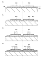
はじめに、半導体装置に用いる半導体基板(SOI基板)の作製方法について、図1乃至3を参照して説明する。 First, a method for manufacturing a semiconductor substrate (SOI substrate) used for a semiconductor device will be described with reference to FIGS.
はじめに、ベース基板100を用意する(図1(A)参照)。ベース基板100には、液晶表示装置などに使用されている透光性を有するガラス基板を用いることができる。ガラス基板としては、歪み点が580℃以上680℃以下(好ましくは、600℃以上680℃以下)であるものを用いると良いが、これに限られない。なお、ガラス基板には、例えば、アルミノシリケートガラス、アルミノホウケイ酸ガラス、バリウムホウケイ酸ガラスなどのガラス材料が用いられている。
First, a
なお、ベース基板100としては、ガラス基板の他、セラミック基板、石英基板やサファイア基板などの絶縁体でなる絶縁性基板、金属やステンレスなどの導電体でなる導電性基板などを用いることもできる。
Note that as the
ベース基板100の表面には絶縁層を形成しても良い。該絶縁層を構成する材料としては、酸化珪素、窒化珪素、酸化窒化珪素、窒化酸化珪素、酸化ゲルマニウム、窒化ゲルマニウム、酸化窒化ゲルマニウム、窒化酸化ゲルマニウムなどの、珪素またはゲルマニウムを組成に含む絶縁材料を用いることができる。また、酸化アルミニウム、酸化タンタル、酸化ハフニウムなどの金属の酸化物、窒化アルミニウムなどの金属の窒化物、酸化窒化アルミニウムなどの金属の酸化窒化物、窒化酸化アルミニウムなどの金属の窒化酸化物を用いることもできる。
An insulating layer may be formed on the surface of the
なお、本明細書において、酸化窒化物とは、その組成において、窒素よりも酸素の含有量(原子数)が多いものを示し、例えば、酸化窒化珪素とは、酸素が50原子%以上70原子%以下、窒素が0.5原子%以上15原子%以下、珪素が25原子%以上35原子%以下、水素が0.1原子%以上10原子%以下の範囲で含まれるものをいう。また、窒化酸化物とは、その組成において、酸素よりも窒素の含有量(原子数)が多いものを示し、例えば、窒化酸化珪素とは、酸素が5原子%以上30原子%以下、窒素が20原子%以上55原子%以下、珪素が25原子%以上35原子%以下、水素が10原子%以上25原子%以下の範囲で含まれるものをいう。但し、上記範囲は、ラザフォード後方散乱法(RBS:Rutherford Backscattering Spectrometry)や、水素前方散乱法(HFS:Hydrogen Forward Scattering)を用いて測定した場合のものである。また、構成元素の含有比率の合計は100原子%を超えない。 Note that in this specification, an oxynitride indicates a composition whose oxygen content (number of atoms) is higher than that of nitrogen. For example, silicon oxynitride is oxygen in an amount of 50 atomic% to 70 atoms. % Or less, nitrogen is 0.5 atomic% to 15 atomic%, silicon is 25 atomic% to 35 atomic%, and hydrogen is 0.1 atomic% to 10 atomic%. In addition, a nitrided oxide indicates a composition whose nitrogen content (number of atoms) is higher than that of oxygen. For example, silicon nitride oxide refers to an oxygen content of 5 atomic% to 30 atomic% and nitrogen content. It includes 20 atomic% to 55 atomic%, silicon in a range of 25 atomic% to 35 atomic%, and hydrogen in a range of 10 atomic% to 25 atomic%. However, the above ranges are those measured using Rutherford Backscattering Spectrometry (RBS) or Hydrogen Forward Scattering (HFS). Further, the total content ratio of the constituent elements does not exceed 100 atomic%.
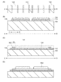
次に、半導体基板110を用意する(図1(B)参照)。ここで、図1(B)は半導体基板110の断面図である。半導体基板110を薄片化した半導体層をベース基板100に貼り合わせることで、半導体基板が作製される。半導体基板110としては単結晶半導体基板を用いることが好ましいが、多結晶半導体基板を用いることもできる。また、シリコン、ゲルマニウム、シリコン−ゲルマニウム、炭化シリコンなどの第14属元素でなる半導体基板を用いることができる。もちろん、ガリウムヒ素、インジウムリンなどの化合物半導体でなる半導体基板を用いてもよい。本実施の形態においては、半導体基板110として、単結晶シリコン基板を用いる。半導体基板110のサイズに制限は無いが、8インチ(200mm)以上(例えば、12インチ(300mm)、18インチ(450mm)等)の円形の半導体基板を、矩形に加工して用いることが好ましい。なお、図2には、円形の半導体基板200を、矩形の半導体基板110に加工した様子を示している。ここで、円形の半導体基板200はオリエンテーションフラット202を有しているが、開示する発明においては、半導体層の面方位や結晶軸の方向は特に限定されない。
Next, the
なお、円形の半導体基板200を矩形に加工する際には、対角線の長さが円形の半導体基板の直径と同程度となるように矩形の半導体基板110を切り出すことが好ましい。これにより、半導体基板200を最大限に利用することができる。例えば、直径8インチ(200mm)の円形の半導体基板からは、対角線の長さが6インチ(150mm)以上8インチ以下の矩形の半導体基板を作製することができる。また、直径12インチ(300mm)の円形の半導体基板からは、対角線の長さが10インチ(250mm)以上12インチ以下の矩形の半導体基板を作製することができる。なお、用いる半導体基板200のサイズが大きくなるにつれて、半導体基板110として利用できない領域は大きくなる。該領域を廃棄することはコストの面で好ましくないため、該領域を矩形の半導体基板204などに加工して、再利用すると良い。
Note that when the
なお、後の工程において、ベース基板100と複数の半導体基板110を貼り合わせることになる。このため、半導体基板110を複数用意し、以下に示す工程を複数回行い又は複数並列して行うことにより、複数の半導体基板110を用意しておくと良い。また、本実施の形態においては、ベース基板100を用意した後、半導体基板110を処理する構成としているが、これは説明の便宜のためであり、開示する発明が該順序に限定して解釈されるものではない。
Note that in a later step, the
半導体基板110を洗浄した後、半導体基板110表面に、絶縁層112を形成する(図1(C)参照)。絶縁層112は単層構造、2層以上の多層構造とすることができる。その厚さは10nm以上400nm以下とすると良い。
After the
絶縁層112を構成する材料としては、酸化珪素、窒化珪素、酸化窒化珪素、窒化酸化珪素、酸化ゲルマニウム、窒化ゲルマニウム、酸化窒化ゲルマニウム、窒化酸化ゲルマニウムなどの、珪素またはゲルマニウムを組成に含む絶縁材料を用いることができる。また、酸化アルミニウム、酸化タンタル、酸化ハフニウムなどの金属の酸化物、窒化アルミニウムなどの金属の窒化物、酸化窒化アルミニウムなどの金属の酸化窒化物、窒化酸化アルミニウムなどの金属の窒化酸化物を用いることもできる。
As a material for forming the insulating
絶縁層112の形成方法としては、CVD法、スパッタ法、半導体基板110の酸化(又は窒化)による方法などを挙げることができる。
As a method for forming the insulating
ベース基板100にアルカリ金属若しくはアルカリ土類金属などの半導体装置の信頼性を低下させる不純物を含むような基板を用いた場合、このような不純物がベース基板100から、半導体層に拡散することを防止できるような層を少なくとも1層以上設けることが好ましい。このような層に用いることができる材料としては、窒化珪素、窒化酸化珪素、窒化アルミニウム又は窒化酸化アルミニウムなどがある。このような材料を用いることで、絶縁層112をバリア層として機能させることができる。
When the
例えば、絶縁層112を単層構造のバリア層として形成する場合には、窒化珪素、窒化酸化珪素、窒化アルミニウム又は窒化酸化アルミニウムを用いて、厚さ10nm以上200nm以下の絶縁層を形成すればよい。
For example, in the case where the insulating
また、絶縁層112をバリア層として機能させ、2層構造とする場合には、例えば、酸化珪素と窒化珪素の積層構造、酸化窒化珪素と窒化珪素の積層構造、酸化珪素と窒化酸化珪素の積層構造、酸化窒化珪素と窒化酸化珪素の積層構造などを採用することができる。この場合、先に記載した材料(酸化珪素又は酸化窒化珪素)からなる層を半導体基板110に接するように設ける。これは、ブロッキング効果の高い材料(窒化珪素又は窒化酸化珪素)からなる層の内部応力が半導体層に作用しないようにするためである。ここで、各層の厚さは10nm以上200nm以下とすることができる。
In the case where the insulating
本実施の形態では、半導体基板110に接する層を、プロセスガスとしてSiH4およびN2Oを用いてプラズマCVD法で形成した酸化窒化珪素からなる層とし、ブロッキング効果の高い層を、プロセスガスとしてSiH4およびNH3を用いてプラズマCVD法で形成した窒化酸化シリコンからなる層とした2層構造を用いる。
In this embodiment, the layer in contact with the
次に、絶縁層112を介して、電界で加速されたイオンでなるイオンビーム130を半導体基板110に照射し、半導体基板110の表面から所定の深さの領域に、損傷領域114を形成する(図1(D)参照)。イオンビームの照射前に絶縁層112を形成することで、イオン照射の際の半導体基板110の汚染を防止し、また、照射されるイオンの衝撃で半導体基板110が損傷することを防止できる。損傷領域114が形成される領域の深さは、イオンビーム130の加速エネルギーとイオンビーム130の入射角によって制御することができる。すなわち、イオンの平均侵入深さと同程度の深さ領域に損傷領域114が形成される。
Next, the
上述の損傷領域114が形成される深さにより、半導体基板110から分離される半導体層の厚さが決定される。損傷領域114が形成される深さは、半導体基板110の表面から50nm以上500nm以下であり、好ましくは50nm以上200nm以下である。
The thickness of the semiconductor layer separated from the
イオンを半導体基板110に照射する際には、イオン注入装置又はイオンドーピング装置を用いることができる。イオン注入装置では、ソースガスを励起してイオン種を生成し、生成されたイオン種を質量分離して、所定の質量を有するイオン種を被処理物に注入する。イオンドーピング装置は、プロセスガスを励起してイオン種を生成し、生成されたイオン種を質量分離せずに被処理物に照射する。なお、質量分離装置を備えているイオンドーピング装置では、イオン注入装置と同様に、質量分離を伴うイオン照射が可能である。
When the
イオンドーピング装置を用いる場合のイオン照射工程は、例えば、以下の条件で行うことができる。
・加速電圧 10kV以上100kV以下(好ましくは30kV以上80kV以下)
・ドーズ量 1×10¹⁶/cm2以上4×1016/cm2以下
・ビーム電流密度 2μA/cm2以上(好ましくは5μA/cm2以上、より好ましくは10μA/cm2以上)
The ion irradiation process in the case of using an ion doping apparatus can be performed under the following conditions, for example.
・ Acceleration voltage: 10 kV to 100 kV (preferably 30 kV to 80 kV)
・
イオンドーピング装置を用いる場合、イオン照射工程のソースガスには水素を含むガスを用いることができる。該ガスを用いることによりイオン種としてH+、H2 +、H3 +を生成することができる。該ガスをソースガスとして用いる場合には、H3 +を多く打ち込むことが好ましい。H3 +イオンを多く打ち込むことで、H+、H2 +を打ち込むよりもイオンの照射効率が向上する。つまり、イオン照射に掛かる時間を短縮することができる。また、損傷領域114での分離がより容易になる。また、H3 +を用いることで、イオンの平均侵入深さを浅くすることができるため、損傷領域114をより浅い領域に形成することができる。
In the case of using an ion doping apparatus, a gas containing hydrogen can be used as a source gas in the ion irradiation step. By using the gas, H + , H 2 + , and H 3 + can be generated as ionic species. When the gas is used as a source gas, it is preferable to implant a large amount of H 3 + . By implanting a large amount of H 3 + ions, the ion irradiation efficiency is improved as compared with implanting H + and H 2 + . That is, the time required for ion irradiation can be shortened. Further, separation at the damaged
イオン注入装置を用いる場合には、質量分離により、H3 +イオンが注入されるようにすることが好ましい。もちろん、H2 +を注入してもよい。ただし、イオン注入装置を用いる場合には、イオン種を選択して注入するため、イオンドーピング装置を用いる場合と比較して、イオンの照射効率が低下する場合がある。 When using an ion implantation apparatus, it is preferable to implant H 3 + ions by mass separation. Of course, H 2 + may be implanted. However, when an ion implantation apparatus is used, since ion species are selected and implanted, ion irradiation efficiency may be reduced as compared with the case where an ion doping apparatus is used.
イオンドーピング装置を用いる場合は、イオンビーム130に、H+、H2 +、H3 +の総量に対してH3 +イオンが70%以上含まれるようにすることが好ましい。H3 +イオンの割合は80%以上とすることがより好ましい。このようにH3 +の割合を高めておくことで、損傷領域114に1×10²⁰atoms/cm3以上の濃度で水素を含ませることが可能である。なお、損傷領域114に5×1020atoms/cm3以上の水素を含ませることで、半導体層の分離が容易になる。
When an ion doping apparatus is used, it is preferable that the
イオン照射工程のソースガスには水素を含むガスの他に、ヘリウムやアルゴンなどの希ガス、フッ素ガスや塩素ガスに代表されるハロゲンガス、フッ素化合物ガス(例えば、BF3)などのハロゲン化合物ガスから選ばれた一種または複数種類のガスを用いることができる。ソースガスにヘリウムを用いる場合は、質量分離を行わなくとも、He+イオンの割合が高いイオンビーム130を作り出すことができる。このようなイオンビーム130を用いることで、損傷領域114を効率よく形成することができる。
As a source gas in the ion irradiation process, in addition to a gas containing hydrogen, a rare gas such as helium or argon, a halogen gas typified by fluorine gas or chlorine gas, or a halogen compound gas such as fluorine compound gas (for example, BF 3 ) One or more kinds of gases selected from the above can be used. When helium is used as the source gas, the
また、イオン照射工程を複数回行うことで、損傷領域114を形成することもできる。この場合、イオン照射工程毎にソースガスを異ならせても良いし、同じソースガスを用いてもよい。例えば、ソースガスとして希ガスを用いてイオンを照射した後、水素を含むガスをソースガスとして用いてイオンを照射することができる。また、初めにハロゲンガス又はハロゲン化合物ガスを用いてイオンを照射し、次に、水素ガスを含むガスを用いてイオンを照射することもできる。
Further, the damaged
以下において、開示する発明の特徴の一であるイオンの照射方法について考察する。 Hereinafter, an ion irradiation method which is one of the features of the disclosed invention will be considered.
開示する発明では、水素(H)に由来するイオン(以下「水素イオン種」と呼ぶ)を単結晶半導体基板に対して照射している。より具体的には、水素ガス又は水素を組成に含むガスを原材料として用い、水素プラズマを発生させ、該水素プラズマ中の水素イオン種を単結晶半導体基板に対して照射している。 In the disclosed invention, the single crystal semiconductor substrate is irradiated with ions derived from hydrogen (H) (hereinafter referred to as “hydrogen ion species”). More specifically, hydrogen plasma or a gas containing hydrogen in its composition is used as a raw material, hydrogen plasma is generated, and a single crystal semiconductor substrate is irradiated with hydrogen ion species in the hydrogen plasma.
(水素プラズマ中のイオン)
上記のような水素プラズマ中には、H+、H2 +、H3 +といった水素イオン種が存在する。ここで、各水素イオン種の反応過程(生成過程、消滅過程)について、以下に反応式を列挙する。
e+H→e+H++e ・・・・・ (1)
e+H2→e+H2 ++e ・・・・・ (2)
e+H2→e+(H2)*→e+H+H ・・・・・ (3)
e+H2 +→e+(H2 +)*→e+H++H ・・・・・ (4)
H2 ++H2→H3 ++H ・・・・・ (5)
H2 ++H2→H++H+H2 ・・・・・ (6)
e+H3 +→e+H++H+H ・・・・・ (7)
e+H3 +→H2+H ・・・・・ (8)
e+H3 +→H+H+H ・・・・・ (9)
(Ions in hydrogen plasma)
Hydrogen ion species such as H + , H 2 + , and H 3 + exist in the hydrogen plasma as described above. Here, the reaction formulas are listed below for the reaction process (generation process, annihilation process) of each hydrogen ion species.
e + H → e + H + + e (1)
e + H 2 → e + H 2 + + e (2)
e + H 2 → e + (H 2 ) * → e + H + H (3)
e + H 2 + → e + (H 2 + ) * → e + H + + H (4)
H 2 + + H 2 → H 3 + + H (5)
H 2 + + H 2 → H + + H + H 2 (6)
e + H 3 + → e + H + + H + H (7)
e + H 3 + → H 2 + H (8)
e + H 3 + → H + H + H (9)
図10に、上記の反応の一部を模式的に表したエネルギーダイアグラムを示す。なお、図10に示すエネルギーダイアグラムは模式図に過ぎず、反応に係るエネルギーの関係を厳密に規定するものではない点に留意されたい。 FIG. 10 shows an energy diagram schematically showing a part of the above reaction. It should be noted that the energy diagram shown in FIG. 10 is only a schematic diagram and does not strictly define the energy relationship related to the reaction.
(H3 +の生成過程)
上記のように、H3 +は、主として反応式(5)により表される反応過程により生成される。一方で、反応式(5)と競合する反応として、反応式(6)により表される反応過程が存在する。H3 +が増加するためには、少なくとも、反応式(5)の反応が、反応式(6)の反応より多く起こる必要がある(なお、H3 +が減少する反応としては他にも(7)、(8)、(9)が存在するため、(5)の反応が(6)の反応より多いからといって、必ずしもH3 +が増加するとは限らない。)。反対に、反応式(5)の反応が、反応式(6)の反応より少ない場合には、プラズマ中におけるH3 +の割合は減少する。
(H 3 + generation process)
As described above, H 3 + is produced mainly by the reaction process represented by the reaction formula (5). On the other hand, as a reaction competing with the reaction formula (5), there is a reaction process represented by the reaction formula (6). For H 3 + to increase, at least, the reaction of the reaction equation (5) is the reaction formula (6) There are many needs to occur from the reaction of (Incidentally, there are also other reactions which the amount of H 3 + ( 7), (8), and (9) are present, and just because the reaction of (5) is more than the reaction of (6), H 3 + does not necessarily increase. On the other hand, when the reaction of the reaction formula (5) is less than the reaction of the reaction formula (6), the ratio of H 3 + in the plasma decreases.
上記反応式における右辺(最右辺)の生成物の増加量は、反応式の左辺(最左辺)で示す原料の密度や、その反応に係る速度係数などに依存している。ここで、H2 +の運動エネルギーが約11eVより小さい場合には(5)の反応が主要となり(すなわち、反応式(5)に係る速度係数が、反応式(6)に係る速度係数と比較して十分に大きくなり)、H2 +の運動エネルギーが約11eVより大きい場合には(6)の反応が主要となることが実験的に確認されている。 The increase amount of the product on the right side (rightmost side) in the above reaction formula depends on the density of the raw material indicated on the left side (leftmost side) of the reaction formula, the rate coefficient related to the reaction, and the like. Here, when the kinetic energy of H 2 + is smaller than about 11 eV, the reaction of (5) becomes the main (that is, the rate coefficient according to the reaction formula (5) is compared with the rate coefficient according to the reaction formula (6)). It has been experimentally confirmed that the reaction (6) is dominant when the kinetic energy of H 2 + is greater than about 11 eV.
荷電粒子は電場から力を受けて運動エネルギーを得る。該運動エネルギーは、電場によるポテンシャルエネルギーの減少量に対応している。例えば、ある荷電粒子が他の粒子と衝突するまでの間に得る運動エネルギーは、その間に通過した電位差分のポテンシャルエネルギーに等しい。つまり、電場中において、他の粒子と衝突することなく長い距離を移動できる状況では、そうではない状況と比較して、荷電粒子の運動エネルギー(の平均)は大きくなる傾向にある。このような、荷電粒子に係る運動エネルギーの増大傾向は、粒子の平均自由行程が大きい状況、すなわち、圧力が低い状況で生じ得る。 A charged particle receives a force from an electric field and obtains kinetic energy. The kinetic energy corresponds to a decrease in potential energy due to an electric field. For example, the kinetic energy obtained until a certain charged particle collides with another particle is equal to the potential energy of the potential difference that has passed during that time. That is, in a situation where a long distance can be moved without colliding with other particles in an electric field, the kinetic energy (average) of charged particles tends to be larger than in situations where this is not the case. Such a tendency of increasing the kinetic energy related to the charged particles may occur in a situation where the mean free path of the particles is large, that is, a situation where the pressure is low.
また、平均自由行程が小さくとも、その間に大きな運動エネルギーを得ることができる状況であれば、荷電粒子の運動エネルギーは大きくなる。すなわち、平均自由行程が小さくとも、電位差が大きい状況であれば、荷電粒子の持つ運動エネルギーは大きくなると言える。 In addition, even if the mean free path is small, the kinetic energy of the charged particles is large if a large kinetic energy can be obtained during that time. That is, even if the mean free path is small, it can be said that the kinetic energy of the charged particles increases if the potential difference is large.
これをH2 +に適用してみる。プラズマの生成に係るチャンバー内のように電場の存在を前提とすれば、該チャンバー内の圧力が低い状況ではH2 +の運動エネルギーは大きくなり、該チャンバー内の圧力が高い状況ではH2 +の運動エネルギーは小さくなる。つまり、チャンバー内の圧力が低い状況では(6)の反応が主要となるため、H3 +は減少する傾向となり、チャンバー内の圧力が高い状況では(5)の反応が主要となるため、H3 +は増加する傾向となる。また、プラズマ生成領域における電場(又は電界)が強い状況、すなわち、ある二点間の電位差が大きい状況ではH2 +の運動エネルギーは大きくなり、反対の状況では、H2 +の運動エネルギーは小さくなる。つまり、電場が強い状況では(6)の反応が主要となるためH3 +は減少する傾向となり、電場が弱い状況では(5)の反応が主要となるため、H3 +は増加する傾向となる。 Let's apply this to H 2 + . Assuming the presence of an electric field as in the chamber related to plasma generation, the kinetic energy of H 2 + increases in a situation where the pressure in the chamber is low, and H 2 + in a situation where the pressure in the chamber is high. The kinetic energy of becomes smaller. That is, since the reaction (6) is dominant in the situation where the pressure in the chamber is low, H 3 + tends to decrease, and in the situation where the pressure in the chamber is high, the reaction (5) is dominant. 3 + tends to increase. Further, in a situation where the electric field (or electric field) in the plasma generation region is strong, that is, in a situation where the potential difference between two points is large, the kinetic energy of H 2 + is large, and in the opposite situation, the kinetic energy of H 2 + is small. Become. In other words, in the situation where the electric field is strong, the reaction (6) is dominant, so H 3 + tends to decrease. In the situation where the electric field is weak, the reaction (5) is dominant, so H 3 + tends to increase. Become.
(イオン源による差異)
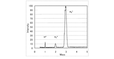
ここで、イオン種の割合(特にH3 +の割合)が異なる例を示す。図21は、100%水素ガス(イオン源の圧力:4.7×10⁻²Pa)から生成されるイオンの質量分析結果を示すグラフである。なお、上記質量分析は、イオン源から引き出されたイオンを測定することにより行った。横軸はイオンの質量である。スペクトル中、質量1、2、3のピークは、それぞれ、H+、H2 +、H3 +に対応する。縦軸は、スペクトルの強度であり、イオンの数に対応する。図21では、質量が異なるイオンの数量を、質量3のイオンを100とした場合の相対比で表している。図21から、上記イオン源により生成されるイオンの割合は、H+:H2 +:H3 +=1:1:8程度となることが分かる。なお、このような割合のイオンは、プラズマを生成するプラズマソース部(イオン源)と、当該プラズマからイオンビームを引き出すための引出電極などから構成されるイオンドーピング装置によっても得ることが出来る。
(Difference due to ion source)
Here, an example in which the ratio of ionic species (particularly, the ratio of H 3 + ) is different will be described. FIG. 21 is a graph showing the results of mass spectrometry of ions generated from 100% hydrogen gas (ion source pressure: 4.7 × 10 −2 Pa). In addition, the said mass spectrometry was performed by measuring the ion withdraw | derived from the ion source. The horizontal axis is the mass of ions. In the spectrum, peaks with
図22は、図21とは異なるイオン源を用いた場合であって、イオン源の圧力がおおよそ3×10⁻³Paの時に、PH3から生成したイオンの質量分析結果を示すグラフである。上記質量分析結果は、水素イオン種に着目したものである。また、質量分析は、イオン源から引き出されたイオンを測定することにより行った。図21と同様、横軸はイオンの質量を示し、質量1、2、3のピークは、それぞれH+、H2 +、H3 +に対応する。縦軸はイオンの数量に対応するスペクトルの強度である。図22から、プラズマ中のイオンの割合はH+:H2 +:H3 +=37:56:7程度であることが分かる。なお、図22はソースガスがPH3の場合のデータであるが、ソースガスとして100%水素ガスを用いたときも、水素イオン種の割合は同程度になる。
FIG. 22 is a graph showing a mass analysis result of ions generated from PH 3 when an ion source different from that in FIG. 21 is used and the pressure of the ion source is approximately 3 × 10 −3 Pa. The mass spectrometry results are focused on hydrogen ion species. Further, mass spectrometry was performed by measuring ions extracted from the ion source. As in FIG. 21, the horizontal axis indicates the mass of ions, and the peaks of
図22のデータを得たイオン源の場合には、H+、H2 +及びH3 +のうち、H3 +が7%程度しか生成されていない。他方、図21のデータを得たイオン源の場合には、H3 +の割合を50%以上(上記の条件では80%程度)とすることが可能である。これは、上記考察において明らかになったチャンバー内の圧力及び電場に起因するものと考えられる。 In the case of the ion source from which the data of FIG. 22 is obtained, only about 7% of H 3 + is generated among H + , H 2 + and H 3 + . On the other hand, in the case of the ion source from which the data of FIG. 21 is obtained, the ratio of H 3 + can be set to 50% or more (about 80% under the above conditions). This is considered to be caused by the pressure and electric field in the chamber, which has been clarified in the above consideration.
(H3 +の照射メカニズム)
図21のような複数のイオン種を含むプラズマを生成し、生成されたイオン種を質量分離しないで単結晶半導体基板に照射する場合、単結晶半導体基板の表面には、H+、H2 +、H3 +の各イオンが照射される。イオンの照射からイオン導入領域形成にかけてのメカニズムを再現するために、以下の5種類のモデルを考える。
1.照射されるイオン種がH+で、照射後もH+(H)である場合
2.照射されるイオン種がH2 +で、照射後もH2 +(H2)のままである場合
3.照射されるイオン種がH2 +で、照射後に2個のH(H+)に分裂する場合
4.照射されるイオン種がH3 +で、照射後もH3 +(H3)のままである場合
5.照射されるイオン種がH3 +で、照射後に3個のH(H+)に分裂する場合。
(H 3 + irradiation mechanism)
In the case of generating plasma including a plurality of ion species as shown in FIG. 21 and irradiating the single crystal semiconductor substrate without mass separation of the generated ion species, H + and H 2 + are formed on the surface of the single crystal semiconductor substrate. , H 3 + ions are irradiated. In order to reproduce the mechanism from ion irradiation to ion introduction region formation, the following five types of models are considered.
1. 1. When the ion species to be irradiated is H + and is H + (H) even after irradiation. 2. When the ion species to be irradiated is H 2 + and remains H 2 + (H 2 ) after irradiation 3. When the ion species to be irradiated is H 2 + and splits into two H (H + ) after
(シミュレーション結果と実測値との比較)
上記のモデルを基にして、水素イオン種をSi基板に照射する場合のシミュレーションを行った。シミュレーション用のソフトウェアとしては、SRIM(the Stopping and Range of Ions in Matter:モンテカルロ法によるイオン導入過程のシミュレーションソフトウェア、TRIM(the Transport of Ions in Matter)の改良版)を用いている。なお、計算の関係上、モデル2ではH2 +を質量2倍のH+に置き換えて計算した。また、モデル4ではH3 +を質量3倍のH+に置き換えて計算した。さらに、モデル3ではH2 +を運動エネルギー1/2のH+に置き換え、モデル5ではH3 +を運動エネルギー1/3のH+に置き換えて計算を行った。
(Comparison between simulation results and measured values)
Based on the above model, a simulation was performed when the Si substrate was irradiated with hydrogen ion species. As simulation software, SRIM (the Stopping and Range of Ions in Matter): simulation software of ion introduction process by Monte Carlo method, TRIM (the Transport of Ions in Matter) is used. Note that, for the calculation, was calculated by replacing the
なお、SRIMは非晶質構造を対象とするソフトウェアではあるが、高エネルギー、高ドーズの条件で水素イオン種を照射する場合には、SRIMを適用可能である。水素イオン種とSi原子の衝突により、Si基板の結晶構造が非単結晶構造に変化するためである。 Note that SRIM is software for an amorphous structure, but SRIM can be applied when irradiating the hydrogen ion species with high energy and high dose. This is because the crystal structure of the Si substrate changes to a non-single crystal structure due to collision between the hydrogen ion species and Si atoms.
図23に、モデル1乃至モデル5を用いて水素イオン種を照射した場合(H換算で10万個照射時)の計算結果を示す。また、図21の水素イオン種を照射したSi基板中の水素濃度(SIMS(Secondary Ion Mass Spectroscopy)のデータ)をあわせて示す。モデル1乃至モデル5を用いて行った計算の結果については、縦軸を水素原子の数で表しており(右軸)、SIMSデータについては、縦軸を水素原子の密度で表している(左軸)。横軸はSi基板表面からの深さである。実測値であるSIMSデータと、計算結果とを比較した場合、モデル2及びモデル4は明らかにSIMSデータのピークから外れており、また、SIMSデータ中にはモデル3に対応するピークも見られない。このことから、モデル2乃至モデル4の寄与は、相対的に小さいことが分かる。イオンの運動エネルギーがkeV程度なのに対して、H−Hの結合エネルギーは数eV程度に過ぎないことを考えれば、モデル2及びモデル4の寄与が小さいのは、Si元素との衝突により、大部分のH2 +やH3 +が、H+やHに分離しているためと思われる。
FIG. 23 shows a calculation result when the hydrogen ion species is irradiated using
以上より、モデル2乃至モデル4については、以下では考慮しない。図24乃至図26に、モデル1及びモデル5を用いて水素イオン種を照射した場合(H換算で10万個照射時)の計算結果を示す。また、図21の水素イオン種を照射したSi基板中の水素濃度(SIMSデータ)及び、上記シミュレーション結果をSIMSデータにフィッティングさせたもの(以下フィッティング関数と呼ぶ)を合わせて示す。ここで、図24は加速電圧を80kVとした場合を示し、図25は加速電圧を60kVとした場合を示し、図26は加速電圧を40kVとした場合を示している。なお、モデル1及びモデル5を用いて行った計算の結果については、縦軸を水素原子の数で表しており(右軸)、SIMSデータ及びフィッティング関数については、縦軸を水素原子の密度で表している(左軸)。横軸はSi基板表面からの深さである。
From the above,
フィッティング関数はモデル1及びモデル5を考慮して以下の計算式により求めることとした。なお、計算式中、X、Yはフィッティングに係るパラメータであり、Vは体積である。
[フィッティング関数]
=X/V×[モデル1のデータ]+Y/V×[モデル5のデータ]
The fitting function is determined by the following calculation formula in consideration of
[Fitting function]
= X / V × [
現実に照射されるイオン種の割合(H+:H2 +:H3 +=1:1:8程度)を考えればH2 +の寄与(すなわち、モデル3)についても考慮すべきであるが、以下に示す理由により、ここでは除外して考えた。
・モデル3に示される照射過程により導入される水素は、モデル5の照射過程と比較して僅かであるため、除外して考えても大きな影響はない(SIMSデータにおいても、ピークが現れていない)。
・モデル5とピーク位置の近いモデル3は、モデル5において生じるチャネリング(結晶の格子構造に起因する元素の移動)により隠れてしまう可能性が高い。すなわち、モデル3のフィッティングパラメータを見積もるのは困難である。これは、本シミュレーションが非晶質Siを前提としており、結晶性に起因する影響を考慮していないことによるものである。
Considering the ratio of ion species actually irradiated (H + : H 2 + : H 3 + = 1: 1: 8 or so), the contribution of H 2 + (that is, model 3) should be considered. For the reasons shown below, it was excluded here.
・ Hydrogen introduced by the irradiation process shown in
-
図27に、上記のフィッティングパラメータをまとめる。いずれの加速電圧においても、導入されるHの数の比は、[モデル1]:[モデル5]=1:42〜1:45程度(モデル1におけるHの数を1とした場合、モデル5におけるHの数は42以上45以下程度)であり、照射されるイオン種の数の比は、[H+(モデル1)]:[H3 +(モデル5)]=1:14〜1:15程度(モデル1におけるH+の数を1とした場合、モデル5におけるH3 +の数は14以上15以下程度)である。モデル3を考慮していないことや非晶質Siと仮定して計算していることなどを考えれば、実際の照射に係るイオン種の比(H+:H2 +:H3 +=1:1:8程度)に近い値が得られていると言える。
FIG. 27 summarizes the above fitting parameters. At any acceleration voltage, the ratio of the number of H to be introduced is about [Model 1]: [Model 5] = 1: 42 to 1:45 (when the number of H in
(H3 +を用いる効果)
図21に示すようなH3 +の割合を高めた水素イオン種を基板に照射することで、H3 +に起因する複数のメリットを享受することができる。例えば、H3 +はH+やHなどに分離して基板内に導入されるため、主にH+やH2 +を照射する場合と比較して、イオンの導入効率を向上させることができる。これにより、半導体基板の生産性向上を図ることができる。また、同様に、H3 +が分離した後のH+やHの運動エネルギーは小さくなる傾向にあるから、薄い半導体層の製造に向いている。
(Effect of using H 3 + )
By irradiating the substrate with hydrogen ion species having an increased H 3 + ratio as shown in FIG. 21, a plurality of merits resulting from H 3 + can be obtained. For example, since H 3 + is separated into H + and H and introduced into the substrate, ion introduction efficiency can be improved as compared with the case of mainly irradiating H + and H 2 +. . Thereby, productivity improvement of a semiconductor substrate can be aimed at. Similarly, since the kinetic energy of H + and H after the separation of H 3 + tends to be small, it is suitable for manufacturing a thin semiconductor layer.
なお、本明細書では、H3 +を効率的に照射するために、図21に示すような水素イオン種を照射可能なイオンドーピング装置を用いる方法について説明している。イオンドーピング装置は廉価で、大面積処理に優れているため、このようなイオンドーピング装置を用いてH3 +を照射することで、半導体特性の向上、大面積化、低コスト化、生産性向上などの顕著な効果を得ることができる。一方で、H3 +の照射を第一に考えるのであれば、イオンドーピング装置を用いることに限定して解釈する必要はない。 Note that in this specification, a method is described in which an ion doping apparatus capable of irradiation with hydrogen ion species as illustrated in FIG. 21 is used in order to efficiently perform irradiation with H 3 + . Since the ion doping apparatus is inexpensive and excellent in large area processing, irradiation with H 3 + using such an ion doping apparatus improves the semiconductor characteristics, increases the area, reduces the cost, and improves the productivity. A remarkable effect such as can be obtained. On the other hand, if the irradiation with H 3 + is considered first, there is no need to interpret it limited to using an ion doping apparatus.
イオン照射により損傷領域114を形成した後、絶縁層112上に、接合層116を形成する(図1(E)参照)。接合層116は、平滑な親水性の表面を有する層である。このような接合層116としては、化学的な反応により形成される絶縁層を用いることが好ましく、中でも酸化珪素を用いた絶縁層を用いることが好ましい。接合層116の厚さは10nm以上200nm以下とすることができる。好ましい厚さは10nm以上100nm以下であり、より好ましくは20nm以上50nm以下である。なお、接合層116を形成する工程において、半導体基板110の加熱温度は損傷領域114に導入された元素や分子が離脱しない温度とする必要がある。具体的には、加熱温度は400℃以下とすることが好ましい。
After the damaged
接合層116として、酸化珪素からなる絶縁層をプラズマCVD法で形成する場合には、シリコンのソースガスとして有機シランガスを用いることが好ましい。酸素のソースガスとしては酸素(O2)ガスを用いることができる。有機シランガスとしては、珪酸エチル(TEOS:化学式Si(OC2H5)4)、テトラメチルシラン(TMS:化学式Si(CH3)4)、テトラメチルシクロテトラシロキサン(TMCTS)、オクタメチルシクロテトラシロキサン(OMCTS)、ヘキサメチルジシラザン(HMDS)、トリエトキシシラン(SiH(OC2H5)3)、トリスジメチルアミノシラン(SiH(N(CH3)2)3)などを用いることができる。また、シリコンのソースガスとしては有機シランガス以外にも、シラン(SiH4)やジシラン(Si2H6)などを用いることができる。
In the case where an insulating layer made of silicon oxide is formed as the
プラズマCVD法以外にも、熱CVD法を用いることで酸化シリコン膜を形成することができる。この場合、シリコンのソースガスとしてはシラン(SiH4)やジシラン(Si2H6)などを、酸素のソースガスとしては酸素(O2)ガスや一酸化二窒素(N2O)ガスなどを用いることができる。加熱温度は200℃以上500℃以下とすることが好ましい。 In addition to the plasma CVD method, a silicon oxide film can be formed by using a thermal CVD method. In this case, silane (SiH 4 ), disilane (Si 2 H 6 ), or the like is used as the source gas for silicon, and oxygen (O 2 ) gas, dinitrogen monoxide (N 2 O) gas, or the like is used as the source gas for oxygen. Can be used. The heating temperature is preferably 200 ° C. or more and 500 ° C. or less.
上記した方法により絶縁層112、損傷領域114、接合層116が設けられた複数の半導体基板110を用意し、ベース基板100と該複数の半導体基板110を貼り合わせる(図1(F)参照)。具体的には、ベース基板100、及び接合層116が形成された半導体基板110を超音波洗浄などの方法で洗浄し、その後、ベース基板100と接合層116を密着させる。これにより、ベース基板100と接合層116が接合する。なお、接合のメカニズムとしては、ファン・デル・ワールス力が関わるメカニズムや、水素結合が関わるメカニズムなどが考えられる。
A plurality of
このように、接合層116として、有機シランを用いてプラズマCVD法で形成した酸化珪素からなる層や、熱CVD法で形成した酸化珪素からなる層などを用いることで、ベース基板100と接合層116を常温で接合することができる。これにより、ベース基板100として、ガラス基板をはじめとする耐熱性の低い基板を用いることが可能となる。
As described above, as the
ベース基板100と接合層116の結合力をより強固なものにするために、ベース基板100の表面を酸素プラズマ処理又はオゾン処理して、その表面を親水性にしても良い。この処理によってベース基板100の表面に水酸基が付加されるため、接合層116との接合界面に水素結合を形成することができる。なお、ベース基板100上に絶縁層を形成する場合には、該絶縁層の表面を親水性にする処理を行ってもよい。
In order to make the bonding force between the
ベース基板100と半導体基板110を密着させた後には、加熱処理又は加圧処理を行っても良い。加熱処理又は加圧処理を行うことで、ベース基板100と接合層116の結合力を向上させることができる。加熱処理を施す場合には、ベース基板の加熱による膨張、収縮の影響が顕著に現れない温度で行うことが好ましい。加圧処理を施す場合には、接合界面に垂直な方向に力が加わるように圧力を加えると良い。加える圧力はベース基板100及び半導体基板110の強度を考慮して決定することができる。
After the
なお、本実施の形態においては、複数の半導体基板110を用意してベース基板100と貼り合わせる構成としたが、開示する発明はこれに限られるものではない。例えば、半導体基板110が十分に大きいものであれば(例えば、半導体基板110とベース基板100が同等の大きさであれば)、一つの半導体基板110のみをベース基板100に貼り合わせる構成としても良い。
Note that although a plurality of
次に、半導体基板110を半導体基板118と半導体層120に分離する(図1(G)参照)。半導体基板110の分離は、ベース基板100と半導体基板110を貼り合わせた後、半導体基板110を加熱することにより行う。この場合にも、ベース基板の加熱による膨張、収縮の影響が顕著に現れない温度で行うことが好ましい。例えば、ベース基板100としてガラス基板を用いる場合には、400℃以上650℃以下とすることが好ましい。
Next, the
上述のような加熱処理を行うことにより、損傷領域114に形成された微小な空孔の体積変化が生じ、損傷領域114に亀裂が生ずる。その結果、損傷領域114に沿って半導体基板110が分離する。接合層116はベース基板100と接合しているので、ベース基板100上には半導体基板110から分離された半導体層120が残存することになる。また、この加熱処理で、ベース基板100と接合層116の接合界面が加熱されるため、接合界面に共有結合が形成され、ベース基板100と接合層116の結合力が向上する。
By performing the heat treatment as described above, a volume change of minute holes formed in the damaged
以上により、ベース基板100に複数の半導体層120が設けられた半導体基板140が作製される。半導体基板140は、ベース基板100上に、接合層116、絶縁層112、半導体層120が順に積層された多層構造の基板であり、ベース基板100と接合層116の界面において接合が形成されている。また、ベース基板100上には、複数の半導体層120が設けられている。
As described above, the
図3は、上記工程によって作製された半導体基板140の構成例を示す平面図である。図3(A)及び(B)は、ベース基板100として、サイズが600mm×720mmであるマザーガラスを用いる場合の半導体基板140の構成例であり、図3(C)は、ベース基板100として、サイズが730mm×920mmである第4世代のマザーガラスを用いる場合の半導体基板140の構成例である。600mm×720mmのマザーガラスに代えて、620mm×750mmのマザーガラスを用いても良い。その他にも、680mm×880mm(第4世代)、1100mm×1300mm(第5世代)、1500mm×1850mm(第6世代)、1870mm×2200mm(第7世代)、2200mm×2400mm(第8世代)など、大型の基板をベース基板100として用いることができる。
FIG. 3 is a plan view showing a configuration example of the
図3(A)では、ベース基板100上に、2行2列に半導体層120が配置されている。該半導体層120のサイズは、280mm×350mmであり、対角線の長さは約18インチである。半導体層120同士の間隔は、x方向(図面横方向)、y方向(図面縦方向)、共に10mmであり、ベース基板100の縁から半導体層120までの距離は、x方向、y方向、共に5mmである。図3(A)における半導体層120は、直径18インチの半導体基板を矩形に加工した半導体基板を用いて形成される。
In FIG. 3A, the semiconductor layers 120 are arranged in two rows and two columns over the
図3(B)では、ベース基板100上に、3行3列に半導体層120が配置されている。該半導体層120のサイズは、184mm×230mmであり、対角線の長さは約12インチである。半導体層120同士の間隔は、x方向、y方向、共に10mmであり、ベース基板100の縁から半導体層120までの距離は、x方向、y方向、共に5mmである。図3(B)における半導体層120は、直径12インチの半導体基板を矩形に加工した半導体基板を用いて形成される。
In FIG. 3B, the semiconductor layers 120 are arranged in 3 rows and 3 columns over the
図3(C)では、ベース基板100上に、3行2列に半導体層120が配置されている。該半導体層120のサイズは、280mm×350mm(350mm×280mm)であり、対角線の長さは約18インチである。半導体層120同士の間隔は、x方向が10mm、y方向が20mmであり、ベース基板100の縁から半導体層120までの距離は、x方向が10mm、y方向が20mmである。図3(C)における半導体層120は、図3(A)の場合と同様に、直径18インチの半導体基板を矩形に加工した半導体基板を用いて形成される。
In FIG. 3C, the semiconductor layers 120 are arranged in 3 rows and 2 columns over the
なお、上述の半導体基板140の構成は一例にすぎず、開示する発明が該構成に限定して解釈されるものではない。例えば、半導体層120同士の間隔を狭めて、連続的に半導体層120を配置しても良い。また、より大きなベース基板100を用いてもよいし、より大きな半導体層120を形成しても良い。
Note that the above structure of the
次に、半導体基板140の後処理工程について、図4及び5を参照して説明する。
Next, the post-processing process of the
はじめに、図1(G)に示す状態の半導体基板140を用意し、半導体層120上に、半導体層120をパターニングするためのマスク132を形成する(図4(A)参照)。なお、マスク132は、フォトリソグラフィ法やインクジェット法を用いて形成することができる。ここで、マスクの形状、面積等は任意であるが、半導体層120を所望の形状、面積等に加工できるように形成する。
First, the
次に、半導体層120をパターニングして、複数の半導体領域122を形成する(図4(B)参照)。該パターニングは、ドライエッチング又はウエットエッチングにより行うことができる。ドライエッチングは異方性が強く、ウエットエッチングは等方性が強いという特徴を有している。ここで、半導体領域122は、半導体素子(例えば、トランジスタ)を1乃至104個程度作製できる大きさとすることが好ましい。具体的には、例えば、1mm2以上10000mm2以下(好ましくは25mm2以上2500mm2以下、より好ましくは100mm2以上150mm2以下)程度の面積となるように形成することができる。半導体領域122が大きすぎる場合には熱応力に起因する問題の解消が十分ではなくなり、半導体領域が小さすぎる場合には半導体素子の作製が困難になるためである。ここで、半導体領域122の周縁部は後に除去することになるため、該除去領域を考慮して半導体領域122の大きさを決定する必要がある。なお、半導体領域122同士の間隔については任意に決定することができる。
Next, the
上記半導体層120のパターニングの際には、絶縁層112はパターニングせずに残存させることが望ましい。絶縁層112をパターニングしないことにより、半導体領域122の下部にはバリア層として機能する絶縁層112が存在することとなり、ベース基板100中に含まれる不純物元素(例えば、ナトリウムやカリウム等のアルカリ金属や、マグネシウム、カルシウム等のアルカリ土類金属、鉄、銅、ニッケル等の遷移金属)の半導体層への侵入を防止できるためである。
In patterning the
上述のように、複数の半導体領域122を形成することにより、後のレーザー光の照射処理や、加熱処理に伴う熱応力の影響を緩和して、欠陥や膜剥がれの発生を抑制することができる。なお、パターニングの終了後には、マスク132は除去することとする。
As described above, by forming the plurality of
上記工程により作製された複数の半導体領域122には、分離工程やイオン照射工程に起因する欠陥が存在し、また、その表面の平坦性は損なわれている。このような凹凸のある半導体領域122の表面に、薄く、且つ、高い絶縁耐圧のゲート絶縁層を形成することは困難である。また、半導体領域122の欠陥の存在により、ゲート絶縁層との界面における局在準位密度が高くなるなど、半導体素子の性能及び信頼性が低下する。そのため、次に、半導体領域122の表面を平坦化し、欠陥を減少させる処理を行う。
In the plurality of
本実施の形態において、半導体領域122の表面の平坦化、及び欠陥の減少は、半導体領域122にレーザー光134を照射することで実現される(図4(C)参照)。レーザー光134を半導体領域122の上面側から照射することで、半導体領域122上面を溶融させる。溶融後、半導体領域122が冷却、固化することで、その上面の平坦性が向上し、欠陥が減少した半導体領域124が得られる(図4(D)参照)。本実施の形態では、レーザー光134を用いているため、ベース基板を加熱する必要が無く、ベース基板100の温度上昇が抑えられる。このため、ガラス基板のような耐熱性の低い基板をベース基板100に用いることが可能になる。また、研磨処理を行わずとも十分な平坦性を確保することができる。もちろん、ベース基板の耐熱温度の範囲内における加熱を伴う構成としても良い。ベース基板を加熱することにより、比較的低いエネルギー密度のレーザー光を用いる場合であっても、欠陥の低減を効果的に進めることができる。
In this embodiment mode, planarization of the surface of the
なお、レーザー光134の照射による半導体領域122の溶融は、部分溶融とする必要がある。完全溶融させた場合には、液相となった半導体領域122における無秩序な核発生により、半導体領域122が再結晶化(微結晶化)することとなり、半導体領域124の結晶性が低下してしまうためである。部分溶融させることにより、溶融されていない固相部分から結晶成長が進行する。これにより、半導体領域122の欠陥を減少させることができる。なお、完全溶融とは、半導体領域122が絶縁層112との界面まで溶融され、液体状態になることをいう。他方、部分溶融とは、この場合、上部は溶融して液相となるが、下部は溶融せずに固相のままであることをいう。
Note that the melting of the
レーザー光の照射には、パルス発振レーザーを用いることが好ましい。これは、瞬間的に高エネルギーのパルスレーザー光を発振することができ、部分溶融状態を作り出すことが容易となるためである。発振周波数は、1Hz以上10MHz以下程度とすることが好ましい。より好ましくは、10Hz以上1MHz以下である。上述のパルス発振レーザーとしては、Arレーザー、Krレーザー、エキシマ(ArF、KrF、XeCl)レーザー、CO2レーザー、YAGレーザー、YVO4レーザー、YLFレーザー、YAlO3レーザー、GdVO4レーザー、Y2O3レーザー、ルビーレーザー、アレキサンドライトレーザー、Ti:サファイアレーザー、銅蒸気レーザー、金蒸気レーザー等を用いることができる。なお、部分溶融させるためにはパルス発振レーザーを用いることが好ましいが、これに限定して解釈されるものではない。すなわち、連続発振レーザーの使用を除外するものではない。なお、連続発振レーザーとしては、Arレーザー、Krレーザー、CO2レーザー、YAGレーザー、YVO4レーザー、YLFレーザー、YAlO3レーザー、GdVO4レーザー、Y2O3レーザー、ルビーレーザー、アレキサンドライトレーザー、Ti:サファイアレーザー、ヘリウムカドミウムレーザー等がある。 A pulsed laser is preferably used for laser light irradiation. This is because high-energy pulsed laser light can be instantaneously oscillated, and it becomes easy to create a partially molten state. The oscillation frequency is preferably about 1 Hz to 10 MHz. More preferably, it is 10 Hz or more and 1 MHz or less. As the above-mentioned pulsed laser, Ar laser, Kr laser, excimer (ArF, KrF, XeCl) laser, CO 2 laser, YAG laser, YVO 4 laser, YLF laser, YAlO 3 laser, GdVO 4 laser, Y 2 O 3 Laser, ruby laser, alexandrite laser, Ti: sapphire laser, copper vapor laser, gold vapor laser, or the like can be used. In order to partially melt, it is preferable to use a pulsed laser, but it is not limited to this. That is, the use of a continuous wave laser is not excluded. As the continuous wave laser, Ar laser, Kr laser, CO 2 laser, YAG laser, YVO 4 laser, YLF laser, YAlO 3 laser, GdVO 4 laser, Y 2 O 3 laser, ruby laser, alexandrite laser, Ti: There are sapphire laser, helium cadmium laser and the like.
レーザー光134の波長は、半導体領域122に吸収される波長とする必要がある。その波長は、レーザー光の表皮深さ(skin depth)などを考慮して決定すればよい。例えば、250nm以上700nm以下の範囲とすることができる。また、レーザー光134のエネルギー密度は、レーザー光134の波長、レーザー光の表皮深さ、半導体領域122の膜厚などを考慮して決定することができる。例えば、300mJ/cm2以上800mJ/cm2以下の範囲とすることができる。なお、上記エネルギー密度の範囲は、パルス発振レーザーとしてXeClエキシマレーザー(波長:308nm)を用いた場合の一例である。
The wavelength of the
なお、イオン照射工程においてイオンの侵入深さを調節し、半導体領域122の厚さを50nmより大きくすることで、レーザー光134のエネルギー密度の調節が容易になる。これにより、レーザー光134の照射による半導体領域122表面の平坦性の向上、および結晶性の向上を、歩留まりよく実現することができる。なお、半導体領域122を厚くするとレーザー光134のエネルギー密度を高くする必要が出てくるため、半導体領域122の厚さは200nm以下としておくことが好ましい。
Note that the energy density of the
レーザー光134の照射は、大気雰囲気のような酸素を含む雰囲気、または窒素雰囲気のような不活性雰囲気で行うことができる。不活性雰囲気中でレーザー光134を照射するには、気密性のあるチャンバー内の雰囲気を制御し、該チャンバー内でレーザー光134を照射すればよい。チャンバーを用いない場合は、レーザー光134の被照射面に窒素ガスなどの不活性ガスを吹き付けることで、窒素雰囲気を形成することもできる。
Irradiation with the
なお、窒素などの不活性雰囲気においてレーザー光134を照射する方が、大気雰囲気で照射するよりも半導体領域122の平坦性を向上させる効果は高い。また、大気雰囲気よりも不活性雰囲気のほうがクラックやリッジの発生を抑える効果が高く、レーザー光134の使用可能なエネルギー密度の範囲が広くなる。なお、レーザー光134の照射は、真空中で行ってもよい。真空中でレーザー光134を照射した場合には、不活性雰囲気における照射と同等の効果を得ることができる。
Note that the irradiation with the
上述のようにレーザー光134を照射した後には、半導体領域124の膜厚を小さくする薄膜化工程を行っても良い。半導体領域124の薄膜化には、ドライエッチングまたはウエットエッチングの一方又は双方を組み合わせたエッチング処理又はエッチバック処理を適用すればよい。例えば、半導体基板110がシリコン基板の場合、SF6と02をプロセスガスに用いたドライエッチング処理で、半導体領域124を薄くすることができる。半導体領域の膜厚を小さくする処理は、レーザー光の照射前に行っても良い。レーザー光の照射と、エッチング処理又はエッチバック処理を組み合わせて用いることにより、半導体層表面の凹凸、欠陥等を著しく低減することができる。
After the
また、レーザー光134の照射前後のいずれか又は両方において、ベース基板100の耐熱温度以下における加熱処理を施しても良い。これにより、レーザー光134の照射では修復できない微細な欠陥を修復することができる。当該加熱処理は、例えば、GRTA(Gas Rapid Thermal Annealing)法や、LRTA(Lamp Rapid Thermal Annealing)法などのRTA法を用いて行うことができる。表面の平坦性等に大きな問題がない場合には、レーザー光の照射に代えて、上記の加熱処理のみを施す構成としても良い。もちろん、上述の加熱処理又はエッチング処理若しくはエッチバック処理を常に用いる必要はない。
Further, heat treatment at a temperature lower than or equal to the heat resistance temperature of the
開示する発明では、大面積の半導体層を半導体領域に分離した後にレーザー光の照射処理又は加熱処理を施している。これにより、半導体領域に分離する前にレーザー光を照射し又は加熱処理を施す場合と比較して、半導体層とベース基板(又は絶縁層等)との熱膨張係数の違いにより生じる熱応力の影響を緩和することができる。つまり、熱膨張係数の異なる材料同士の接触面積が大きいほど、熱応力の影響は大きくなるが、半導体層をパターニングすることにより、接触面積自体を小さくして熱応力を低減している。また、半導体層が大面積の場合には、端部に応力が集中し、欠陥や膜剥がれの要因となりがちであるが、半導体層を半導体領域に分離することにより(すなわち、面積を低減することにより)、各半導体領域に応力を分散させることができるため、大面積ゆえに生じる応力の問題を解消することができる。 In the disclosed invention, after a large-area semiconductor layer is separated into semiconductor regions, laser light irradiation treatment or heat treatment is performed. As a result, the effect of thermal stress caused by the difference in thermal expansion coefficient between the semiconductor layer and the base substrate (or insulating layer, etc.) compared to the case where laser light is irradiated or heat treatment is performed before the semiconductor region is separated. Can be relaxed. That is, the larger the contact area between materials having different thermal expansion coefficients, the greater the influence of thermal stress, but by patterning the semiconductor layer, the contact area itself is reduced to reduce thermal stress. In addition, when the semiconductor layer has a large area, stress tends to concentrate on the edges, which tends to cause defects and film peeling. However, by separating the semiconductor layer into semiconductor regions (that is, reducing the area) Therefore, since the stress can be dispersed in each semiconductor region, the problem of stress caused by the large area can be solved.
以上により、半導体領域124を有する半導体基板142が得られる(図4(D)参照)。図5は、一つの半導体層120から3行3列の半導体領域124を形成した構成の半導体基板142を示す平面図である。図5における半導体基板142は、図3(A)に示した半導体基板140を加工したものに対応する。なお、図5は半導体基板142の一例を示すにすぎず、開示する発明の半導体基板142が該構成に限定して解釈されるものではない。特に、半導体領域124の形成の仕方(面積、配置等)については、適宜変更することができる。
Through the above steps, the
次に、図6乃至9を参照して、上記の半導体基板142を用いた半導体装置の作製方法について説明する。ここでは、半導体装置の一例として複数のトランジスタからなる半導体装置の作製方法について説明することとする。なお、以下において示すトランジスタを組み合わせて用いることで、様々な半導体装置を形成することができる。
Next, a method for manufacturing a semiconductor device using the
図6(A)は、図5において示した半導体基板142の一部を示す平面図である。また、図6(B)は、図6(A)のA−Bにおける断面図である。また、図6(C)は、図6(B)におけるC−D(図6(B)の破線で囲まれた領域)を拡大した断面図である。なお、図6(C)においては、半導体領域124の中央部分を一部省略している。
FIG. 6A is a plan view illustrating a part of the
図6(C)では、半導体領域124の端部に、半導体特性が低下した領域602が存在する。該領域602は、半導体領域に対するレーザー光の照射や加熱処理などによる溶融再結晶化により、端部に応力が残留することで生じるものと考えられる。開示する発明では、該半導体特性が低下した領域602を用いずにトランジスタを作製する。具体的には、半導体領域124の一辺の長さLaに対して、両端部の長さLbに相当する領域を除去し、残存した領域を用いてトランジスタを作製する。ここで、Lbは、Laの10%以上20%以下とすることが好ましい。
In FIG. 6C, a
領域602の除去及びトランジスタの活性層の作製のため、半導体領域124上にマスク604を形成する(図6(D)参照)。なお、マスク604は、フォトリソグラフィ法やインクジェット法を用いて形成することができる。ここで、マスクの形状、面積等はトランジスタの活性層に合わせて決定すればよいが、領域602を除去することができるように形成する必要がある。
A
その後、マスク604を用いて半導体領域124をパターニングし、島状の半導体層を複数形成する。ここでは、代表的に、半導体層606及び半導体層608について示す(図7(A)参照)。該パターニングは、ドライエッチング又はウエットエッチングにより行うことができる。ここで、ドライエッチングは異方性が強く、ウエットエッチングは等方性が強いという特徴を有している。これらの特徴を利用して、テーパー形状となるように島状の半導体層を形成しても良いし、島状の半導体層の端部が丸みを帯びた形状となるように加工しても良い。例えば、等方性が強いエッチングを用いることにより、島状の半導体層の端部に丸みを帯びさせることができる。また、いわゆるICP(Inductively Coupled Plasma:誘導結合型プラズマ)エッチング法を用い、エッチング条件(コイル型の電極層に印加される電力量、基板側の電極層に印加される電力量、基板側の電極温度等)を適宜調節し、所望のテーパー形状となるように島状の半導体層を形成することもできる。テーパー形状は、マスクの形状によって制御することもできる。島状の半導体層がテーパー形状となるように形成されることで、後に形成される絶縁層や導電層の被覆が良好に行われるため、絶縁層や導電層の段切れを防止することができる。また、島状の半導体層の端部が丸みを帯びることにより、電界の集中を緩和して半導体素子に不具合が生じることを防止できる。
After that, the
半導体層606及び半導体層608には、トランジスタのしきい値電圧を制御するために、硼素、アルミニウム、ガリウムなどのp型不純物、若しくはリン、砒素などのn型不純物を添加しても良い。不純物を添加する領域、および添加する不純物の種類は、適宜変更することができる。例えば、nチャネル型トランジスタの形成領域にはp型不純物を添加し、pチャネル型トランジスタの形成領域にはn型不純物を添加することができる。上述の不純物を添加する際には、ドーズ量が1×10¹⁵/cm2以上1×1017/cm2以下程度となるように行えばよい。
In order to control the threshold voltage of the transistor, a p-type impurity such as boron, aluminum, or gallium, or an n-type impurity such as phosphorus or arsenic may be added to the
次に、半導体層606と半導体層608を覆うように、ゲート絶縁層610を形成する(図7(B)参照)。ここでは、プラズマCVD法を用いて、酸化珪素膜を単層で形成することとする。その他にも、酸化窒化珪素、窒化酸化珪素、窒化珪素、酸化ハフニウム、酸化アルミニウム、酸化タンタル等を含む膜を、単層構造又は積層構造で形成することによりゲート絶縁層610としても良い。
Next, a
プラズマCVD法以外の作製方法としては、スパッタリング法や、高密度プラズマ処理による酸化または窒化による方法が挙げられる。高密度プラズマ処理は、例えば、ヘリウム、アルゴン、クリプトン、キセノンなどの希ガスと、酸素、酸化窒素、アンモニア、窒素、水素などのガスの混合ガスを用いて行う。この場合、プラズマの励起をマイクロ波の導入により行うことで、低電子温度で高密度のプラズマを生成することができる。このような高密度のプラズマで生成された酸素ラジカル(OHラジカルを含む場合もある)や窒素ラジカル(NHラジカルを含む場合もある)によって、半導体層の表面を酸化または窒化することにより、1nm以上20nm以下、望ましくは2nm以上10nm以下の絶縁層を半導体層に接するように形成する。 As a manufacturing method other than the plasma CVD method, a sputtering method or a method using oxidation or nitridation by high-density plasma treatment can be given. The high-density plasma treatment is performed using a mixed gas of a rare gas such as helium, argon, krypton, or xenon and a gas such as oxygen, nitrogen oxide, ammonia, nitrogen, or hydrogen. In this case, high-density plasma can be generated at a low electron temperature by exciting the plasma by introducing a microwave. By oxidizing or nitriding the surface of the semiconductor layer with oxygen radicals (which may include OH radicals) or nitrogen radicals (which may include NH radicals) generated by such high-density plasma, 1 nm or more An insulating layer of 20 nm or less, preferably 2 nm or more and 10 nm or less is formed so as to be in contact with the semiconductor layer.
上述した高密度プラズマ処理による半導体層の酸化または窒化は固相反応であるため、ゲート絶縁層610と、半導体層606又は半導体層608との界面準位密度をきわめて低くすることができる。また、高密度プラズマ処理により半導体層を直接酸化または窒化することで、形成される絶縁層の厚さのばらつきを抑えることが出来る。また、半導体層が結晶性を有するため、高密度プラズマ処理を用いて半導体層の表面を固相反応で酸化させる場合であっても、結晶粒界における不均一な酸化を抑え、均一性が良く、界面準位密度の低いゲート絶縁層を形成することができる。このように、高密度プラズマ処理により形成された絶縁層をトランジスタのゲート絶縁層の一部または全部に用いることで、特性のばらつきを抑制することができる。
Since the oxidation or nitridation of the semiconductor layer by the high-density plasma treatment described above is a solid-phase reaction, the interface state density between the
プラズマ処理による絶縁層の作製方法のより具体的な一例について説明する。亜酸化窒素(N2O)を、アルゴン(Ar)を用いて1倍以上3倍以下(流量比)に希釈し、10Pa以上30Pa以下の圧力下で3kW以上5kW以下のマイクロ波(2.45GHz)電力を印加して、半導体層606と半導体層608の表面を酸化または窒化させる。この処理により1nm以上10nm以下(好ましくは2nm以上6nm以下)のゲート絶縁層610の下層を形成する。さらに、亜酸化窒素(N2O)とシラン(SiH4)を導入し、10Pa以上30Pa以下の圧力下で3kW以上5kW以下のマイクロ波(2.45GHz)電力を印加して気相成長法により酸化窒化シリコン膜を形成し、ゲート絶縁層610の上層とする。このように、固相反応と気相成長法を組み合わせてゲート絶縁層610を形成することにより、界面準位密度が低く絶縁耐圧の優れたゲート絶縁層610を形成することができる。なお、この場合においては、ゲート絶縁層610は2層構造となる。
A more specific example of a method for manufacturing an insulating layer by plasma treatment will be described. Nitrous oxide (N 2 O) is diluted 1 to 3 times (flow rate ratio) with argon (Ar), and a microwave (2.45 GHz) of 3 kW to 5 kW under a pressure of 10 Pa to 30 Pa. ) Electric power is applied to oxidize or nitride the surfaces of the
或いは、半導体層606と半導体層608を熱酸化させることで、ゲート絶縁層610を形成するようにしても良い。このような熱酸化を用いる場合には、耐熱性の比較的高いベース基板を用いることが好ましい。
Alternatively, the
なお、水素を含むゲート絶縁層610を形成し、その後、350℃以上450℃以下の温度による加熱処理を行うことで、ゲート絶縁層610中に含まれる水素を半導体層606及び半導体層608中に拡散させるようにしても良い。この場合、ゲート絶縁層610として、プラズマCVD法を用いた窒化シリコン又は窒化酸化シリコンを用いることができる。なお、ゲート絶縁層の作製温度は350℃以下とすると良い。このように、半導体層606及び半導体層608に水素を供給することで、半導体層606中、半導体層608中、ゲート絶縁層610と半導体層606の界面、及びゲート絶縁層610と半導体層608の界面における欠陥を効果的に低減することができる。
Note that a
次に、ゲート絶縁層610上に導電層を形成した後、該導電層を所定の形状に加工(パターニング)することで、半導体層606と半導体層608の上方に電極612を形成する(図7(C)参照)。導電層の形成にはCVD法、スパッタリング法等を用いることができる。導電層は、タンタル(Ta)、タングステン(W)、チタン(Ti)、モリブデン(Mo)、アルミニウム(Al)、銅(Cu)、クロム(Cr)、ニオブ(Nb)等の材料を用いて形成することができる。また、上記金属を主成分とする合金材料を用いても良いし、上記金属を含む化合物を用いても良い。または、導電性を付与する不純物元素をドーピングした多結晶珪素などの半導体材料を用いて形成しても良い。
Next, after a conductive layer is formed over the
本実施の形態では電極612を単層の導電層で形成しているが、開示する発明の半導体装置は該構成に限定されない。電極612は積層された複数の導電層で形成されていても良い。2層構造とする場合には、例えば、モリブデン膜、チタン膜、窒化チタン膜等を下層に用い、上層にはアルミニウム膜などを用いればよい。3層構造の場合には、モリブデン膜とアルミニウム膜とモリブデン膜の積層構造や、チタン膜とアルミニウム膜とチタン膜の積層構造などを採用するとよい。
In this embodiment, the
なお、電極612を形成する際に用いるマスクは、酸化珪素や窒化酸化珪素等の材料を用いて形成してもよい。この場合、酸化珪素膜や窒化酸化珪素膜等をパターニングしてマスクを形成する工程が加わるが、レジスト材料を用いたマスクと比較して、エッチング時におけるマスクの膜減りが少ないため、より正確な形状の電極612を形成することができる。また、マスクを用いずに、液滴吐出法を用いて選択的に電極612を形成しても良い。ここで、液滴吐出法とは、所定の組成物を含む液滴を吐出または噴出することで所定のパターンを形成する方法を意味し、インクジェット法などがその範疇に含まれる。
Note that a mask used for forming the
また、ICP(Inductively Coupled Plasma:誘導結合型プラズマ)エッチング法を用い、エッチング条件(コイル型の電極層に印加される電力量、基板側の電極層に印加される電力量、基板側の電極温度等)を適宜調節し、所望のテーパー形状となるように導電層をエッチングすることで、電極612を形成することもできる。また、テーパー形状は、マスクの形状によって制御することもできる。なお、エッチング用ガスとしては、塩素、塩化硼素、塩化珪素もしくは四塩化炭素などの塩素系ガス、四弗化炭素、弗化硫黄もしくは弗化窒素などのフッ素系ガス又は酸素などを適宜用いることができる。
Further, using an ICP (Inductively Coupled Plasma) etching method, etching conditions (amount of power applied to the coil-type electrode layer, a power amount applied to the electrode layer on the substrate side, and an electrode temperature on the substrate side) Etc.) is adjusted as appropriate, and the conductive layer is etched so as to have a desired taper shape, whereby the
次に、図7(D)に示すように、電極612をマスクとして、一導電型を付与する不純物元素を半導体層606、半導体層608に添加する。本実施の形態では、半導体層606にn型を付与する不純物元素(例えばリンまたはヒ素)を、半導体層608にp型を付与する不純物元素(例えばボロン)を添加する。なお、n型を付与する不純物元素を半導体層606に添加する際には、p型の不純物が添加される半導体層608はマスク等で覆い、n型を付与する不純物元素の添加が選択的に行われるようにする。また、p型を付与する不純物元素を半導体層608に添加する際には、n型の不純物が添加される半導体層606はマスク等で覆い、p型を付与する不純物元素の添加が選択的に行われるようにする。又は、半導体層606及び半導体層608に、p型を付与する不純物元素又はn型を付与する不純物元素の一方を添加した後、一方の半導体層のみに、より高い濃度でp型を付与する不純物元素又はn型を付与する不純物元素の他方を添加するようにしても良い。上記不純物の添加により、半導体層606に不純物領域614、半導体層608に不純物領域616が形成される。
Next, as illustrated in FIG. 7D, an impurity element imparting one conductivity type is added to the
次に、図8(A)に示すように、電極612の側面にサイドウォール618を形成する。サイドウォール618は、例えば、ゲート絶縁層610及び電極612を覆うように新たに絶縁層を形成し、垂直方向を主体とした異方性エッチングにより、該絶縁層を部分的にエッチングすることで形成することができる。なお、上記の異方性エッチングにより、ゲート絶縁層610を部分的にエッチングしても良い。本実施の形態においては、電極612下及びサイドウォール618下のゲート絶縁層610以外については除去された構成を示している。サイドウォール618を形成するための絶縁層としては、プラズマCVD法やスパッタリング法等により、珪素、酸化珪素、窒化珪素、酸化窒化珪素、窒化酸化珪素、有機材料などを含む膜を、単層構造又は積層構造で形成すれば良い。本実施の形態では、膜厚100nmの酸化珪素膜をプラズマCVD法によって形成する。また、エッチングガスとしては、CHF3とヘリウムの混合ガスを用いることができる。なお、サイドウォール618を形成する工程は、これらに限定されるものではない。
Next, as illustrated in FIG. 8A, sidewalls 618 are formed on the side surfaces of the
次に、図8(B)に示すように、ゲート絶縁層610、電極612及びサイドウォール618をマスクとして、半導体層606、半導体層608に一導電型を付与する不純物元素を添加する。なお、半導体層606、半導体層608には、それぞれ先の工程で添加した不純物元素と同じ導電型の不純物元素をより高い濃度で添加する。なお、n型を付与する不純物元素を半導体層606に添加する際には、p型の不純物が添加される半導体層608はマスク等で覆い、n型を付与する不純物元素の添加が選択的に行われるようにする。また、p型を付与する不純物元素を半導体層608に添加する際には、n型の不純物が添加される半導体層606はマスク等で覆い、p型を付与する不純物元素の添加が選択的に行われるようにする。
Next, as illustrated in FIG. 8B, an impurity element imparting one conductivity type is added to the semiconductor layers 606 and 608 using the
上記不純物元素の添加により、半導体層606に、一対の高濃度不純物領域620と、一対の低濃度不純物領域622と、チャネル形成領域624とが形成される。また、上記不純物元素の添加により、半導体層608に、一対の高濃度不純物領域626と、一対の低濃度不純物領域628と、チャネル形成領域630とが形成される。高濃度不純物領域620、高濃度不純物領域626はソース又はドレインとして機能し、低濃度不純物領域622、低濃度不純物領域628はLDD(Lightly Doped Drain)領域として機能する。
By the addition of the impurity element, a pair of high-
なお、半導体層606上に形成されたサイドウォール618と、半導体層608上に形成されたサイドウォール618は、キャリアが移動する方向(いわゆるチャネル長に平行な方向)における幅が同じになるように形成しても良いが、該幅が異なるように形成しても良い。pチャネル型トランジスタとなる半導体層608上のサイドウォール618の幅は、nチャネル型トランジスタとなる半導体層606上のサイドウォール618の幅よりも長くすると良い。なぜならば、pチャネル型トランジスタにおいてソース及びドレインを形成するために注入されるボロンは拡散しやすく、短チャネル効果を誘起しやすいためである。pチャネル型トランジスタにおいて、サイドウォール618の幅をより長くすることで、ソース及びドレインに高濃度のボロンを添加することが可能となり、ソース及びドレインを低抵抗化することができる。
Note that the
ソース及びドレインをさらに低抵抗化するために、半導体層606及び半導体層608の一部をシリサイド化したシリサイド層を形成しても良い。シリサイド化は、半導体層に金属を接触させ、加熱処理(例えば、GRTA法、LRTA法など)により、半導体層中の珪素と金属とを反応させて行う。シリサイド層としては、コバルトシリサイド又はニッケルシリサイドを用いると良い。半導体層606や半導体層608が薄い場合には、半導体層606、半導体層608の底部までシリサイド反応を進めても良い。シリサイド化に用いることができる金属材料としては、チタン(Ti)、ニッケル(Ni)、タングステン(W)、モリブデン(Mo)、コバルト(Co)、ジルコニウム(Zr)、ハフニウム(Hf)、タンタル(Ta)、バナジウム(V)、ネオジム(Nd)、クロム(Cr)、白金(Pt)、パラジウム(Pd)等が挙げられる。また、レーザー光の照射などによってもシリサイド層を形成することができる。
In order to further reduce the resistance of the source and drain, a silicide layer in which part of the
上述の工程により、nチャネル型トランジスタ650及びpチャネル型トランジスタ652が形成される。なお、図8(B)に示す段階では、ソース電極又はドレイン電極として機能する導電層は形成されていないが、これらのソース電極又はドレイン電極として機能する導電層を含めてトランジスタと呼ぶこともある。
Through the above steps, an n-
次に、図8(C)に示すように、nチャネル型トランジスタ650、pチャネル型トランジスタ652を覆うように絶縁層632を形成する。絶縁層632は必ずしも設ける必要はないが、絶縁層632を形成することで、アルカリ金属やアルカリ土類金属などの不純物がnチャネル型トランジスタ650、pチャネル型トランジスタ652に侵入することを防止できる。具体的には、絶縁層632を、酸化珪素、窒化珪素、酸化窒化珪素、窒化酸化珪素、窒化アルミニウム、酸化アルミニウムなどの材料を用いて形成するのが望ましい。本実施の形態では、膜厚600nm程度の窒化酸化珪素膜を、絶縁層632として用いる。この場合、上述の水素化の工程は、該窒化酸化珪素膜形成後に行っても良い。なお、本実施の形態においては、絶縁層632を単層構造としているが、積層構造としても良いことはいうまでもない。例えば、2層構造とする場合には、酸化窒化珪素膜と窒化酸化珪素膜との積層構造とすることができる。
Next, as illustrated in FIG. 8C, an insulating
次に、nチャネル型トランジスタ650、pチャネル型トランジスタ652を覆うように、絶縁層632上に絶縁層634を形成する。絶縁層634は、ポリイミド、アクリル、ベンゾシクロブテン、ポリアミド、エポキシ等の、耐熱性を有する有機材料を用いて形成するとよい。また、上記有機材料の他に、低誘電率材料(low−k材料)、シロキサン系樹脂、酸化珪素、窒化珪素、酸化窒化珪素、窒化酸化珪素、PSG(リンガラス)、BPSG(リンボロンガラス)、アルミナ等を用いることもできる。ここで、シロキサン系樹脂とは、シロキサン系材料を出発材料として形成されたSi−O−Si結合を含む樹脂に相当する。シロキサン系樹脂は、置換基に水素の他、フッ素、アルキル基又は芳香族炭化水素のうち少なくとも1種を有していても良い。なお、これらの材料で形成される絶縁層を複数積層させることで、絶縁層634を形成しても良い。また、絶縁層634は、その表面をCMP法などにより平坦化させても良い。
Next, an insulating
絶縁層634の形成には、その材料に応じて、CVD法、スパッタ法、SOG法、スピンコート、ディップ、スプレー塗布、液滴吐出法(インクジェット法、スクリーン印刷、オフセット印刷等)、ドクターナイフ、ロールコーター、カーテンコーター、ナイフコーター等を用いることができる。
Depending on the material, the insulating
次に、半導体層606と半導体層608がそれぞれ一部露出するように絶縁層632及び絶縁層634にコンタクトホールを形成する。そして、図9(A)に示すように、該コンタクトホールを介して半導体層606と半導体層608に接する導電層636、導電層638を形成する。導電層636及び導電層638は、トランジスタのソース電極又はドレイン電極として機能する。なお、本実施の形態においては、コンタクトホール開口時のエッチングに用いるガスとしてCHF3とHeの混合ガスを用いたが、これに限定されるものではない。
Next, contact holes are formed in the insulating
導電層636、導電層638は、CVD法やスパッタリング法等により形成することができる。具体的には、導電層636、導電層638として、アルミニウム(Al)、タングステン(W)、チタン(Ti)、タンタル(Ta)、モリブデン(Mo)、ニッケル(Ni)、白金(Pt)、銅(Cu)、金(Au)、銀(Ag)、マンガン(Mn)、ネオジム(Nd)、炭素(C)、珪素(Si)等を用いることができる。また、上記材料を主成分とする合金を用いても良いし、上記材料を含む化合物を用いても良い。また、導電層636、導電層638は、単層構造としても良いし、積層構造としても良い。
The
アルミニウムを主成分とする合金の例としては、アルミニウムを主成分として、ニッケルを含むものが挙げられる。また、アルミニウムを主成分とし、ニッケルと、炭素または珪素の一方または両方を含むものを挙げることができる。アルミニウムやアルミニウムシリコン(Al−Si)は抵抗値が低く、安価であるため、導電層636、導電層638を形成する材料として適している。特に、アルミニウムシリコンは、パターニングの際のレジストベークによるヒロックの発生を抑制することができるため好ましい。また、珪素の代わりに、アルミニウムに0.5%程度のCuを混入させた材料を用いても良い。
As an example of an alloy containing aluminum as a main component, an alloy containing aluminum as a main component and containing nickel can be given. Further, examples include aluminum as a main component and one or both of nickel and carbon or silicon. Aluminum and aluminum silicon (Al—Si) have low resistance and are inexpensive, and thus are suitable as a material for forming the
導電層636、導電層638を積層構造とする場合には、例えば、バリア膜とアルミニウムシリコン膜とバリア膜の積層構造、バリア膜とアルミニウムシリコン膜と窒化チタン膜とバリア膜の積層構造などを採用するとよい。なお、バリア膜とは、チタン、チタンの窒化物、モリブデンまたはモリブデンの窒化物などを用いて形成された膜である。バリア膜の間にアルミニウムシリコン膜を挟むように導電層を形成すると、アルミニウムやアルミニウムシリコンのヒロックの発生をより一層防止することができる。また、還元性の高い元素であるチタンを用いてバリア膜を形成すると、半導体層606と半導体層608上に薄い酸化膜が形成されていたとしても、バリア膜に含まれるチタンが該酸化膜を還元し、導電層636と半導体層606、及び導電層638と半導体層608のコンタクトを良好なものとすることができる。また、バリア膜を複数積層するようにして用いても良い。その場合、例えば、導電層636、導電層638を、下層からチタン、窒化チタン、アルミニウムシリコン、チタン、窒化チタンのように、5層構造又はそれ以上の積層構造とすることもできる。
In the case where the
また、導電層636、導電層638として、WF6ガスとSiH4ガスから化学気相成長法で形成したタングステンシリサイドを用いても良い。また、WF6を水素還元して形成したタングステンを、導電層636、導電層638として用いても良い。
Alternatively, tungsten silicide formed by a chemical vapor deposition method using WF 6 gas and SiH 4 gas may be used for the
なお、導電層636はnチャネル型トランジスタ650の高濃度不純物領域620に接続されている。導電層638はpチャネル型トランジスタ652の高濃度不純物領域626に接続されている。
Note that the
図9(B)に、図9(A)に示したnチャネル型トランジスタ650及びpチャネル型トランジスタ652の平面図を示す。ここで、図9(B)のC−Dにおける断面が図9(A)に対応している。ただし、図9(B)においては、簡単のため、導電層636、導電層638、絶縁層632、絶縁層634等を省略している。
FIG. 9B is a plan view of the n-
なお、本実施の形態においては、nチャネル型トランジスタ650とpチャネル型トランジスタ652が、それぞれゲート電極として機能する電極612を1つずつ有する場合を例示しているが、開示する発明は該構成に限定されない。開示する発明で作製されるトランジスタは、ゲート電極として機能する電極を複数有し、なおかつ該複数の電極が電気的に接続されているマルチゲート構造を有していても良い。
Note that in this embodiment, the n-
以上により、複数のトランジスタを有する半導体装置を作製することができる。 Through the above steps, a semiconductor device including a plurality of transistors can be manufactured.
開示する発明では、ベース基板にガラス基板等の大型の基板を採用することで、半導体基板の大面積化を図ることができる。さらに、ベース基板に貼り合わせる単結晶半導体基板を大型のものにすることで、半導体基板の作製効率が向上し、半導体基板の大面積化も容易になる。そして、半導体基板を大型にすることで、半導体装置の生産性が向上し、また、大型の半導体装置を作製することも可能になる。また、単結晶半導体層に対してレーザー光を照射することにより、単結晶半導体層表面の平坦性が向上し、欠陥が低減される。また、加熱処理を施すことにより、レーザー光の照射では修復できない微細な欠陥を修復することができる。これにより、半導体素子の特性を向上し、優れた半導体装置を提供することができる。 In the disclosed invention, the use of a large substrate such as a glass substrate for the base substrate can increase the area of the semiconductor substrate. Further, by increasing the size of the single crystal semiconductor substrate to be bonded to the base substrate, the manufacturing efficiency of the semiconductor substrate is improved and the area of the semiconductor substrate can be easily increased. By increasing the size of the semiconductor substrate, the productivity of the semiconductor device can be improved, and a large-sized semiconductor device can be manufactured. Further, by irradiating the single crystal semiconductor layer with laser light, the flatness of the surface of the single crystal semiconductor layer is improved and defects are reduced. Further, by performing heat treatment, fine defects that cannot be repaired by laser light irradiation can be repaired. Thereby, the characteristic of a semiconductor element can be improved and the outstanding semiconductor device can be provided.
また、レーザー光の照射処理の前又は加熱処理の前に単結晶半導体層をパターニングすることで、熱応力による欠陥の増大並びに熱応力による膜剥がれの問題を解消することができる。これにより、半導体素子の性能及び信頼性が向上する。また、パターニングの際に、単結晶半導体層の下地層として形成されている絶縁層を残存させることにより、ベース基板からの汚染物質(不純物元素等)が半導体層に侵入することを防止できるため、半導体装置の信頼性を向上することができる。また、レーザー光の照射や加熱処理によって半導体特性が低下する領域を半導体素子として用いないことにより、半導体素子の特性を向上し、優れた半導体装置を提供することができる。 Further, by patterning the single crystal semiconductor layer before the laser light irradiation treatment or the heat treatment, problems of increase in defects due to thermal stress and film peeling due to thermal stress can be solved. This improves the performance and reliability of the semiconductor element. Further, by leaving an insulating layer formed as a base layer of the single crystal semiconductor layer during patterning, it is possible to prevent contaminants (impurity elements and the like) from the base substrate from entering the semiconductor layer. The reliability of the semiconductor device can be improved. In addition, by not using, as a semiconductor element, a region in which semiconductor characteristics deteriorate due to laser light irradiation or heat treatment, the characteristics of the semiconductor element can be improved and an excellent semiconductor device can be provided.
(実施の形態2)
本実施の形態では、半導体装置の製造方法の別の例について、図11乃至14を参照して説明する。なお、本実施の形態においては、半導体装置の一例として液晶表示装置を挙げて説明するが、開示する発明の半導体装置は液晶表示装置に限られるものではない。
(Embodiment 2)
In this embodiment, another example of a method for manufacturing a semiconductor device will be described with reference to FIGS. Note that in this embodiment, a liquid crystal display device is described as an example of a semiconductor device; however, a semiconductor device of the disclosed invention is not limited to a liquid crystal display device.
はじめに、実施の形態1に示す方法などを用いて作製された、単結晶半導体層を有する半導体基板を用意する(図11(A)参照)。ここでは、絶縁表面を有する基板1100(ベース基板)の上に接合層を含む絶縁層1102、絶縁層1104、単結晶半導体層1106を順に設けた構成を用いて説明するが、開示する発明はこれに限られるものではない。ここで、絶縁層1104は、酸化珪素、窒化珪素、酸化窒化珪素、窒化酸化珪素などの材料を用いて形成することができる。また、絶縁層1104は積層構造であっても良い。詳細については、実施の形態1を参照することができる。なお、該半導体基板は、実施の形態1における半導体基板142に対応し、絶縁層1104は絶縁層112に対応している。
First, a semiconductor substrate having a single crystal semiconductor layer, which is manufactured using the method described in
次に、単結晶半導体層1106を所望の形状にパターニングして、島状の単結晶半導体層を形成する。本実施の形態においても、実施の形態1と同様に、半導体特性が低下した領域が除去されるように単結晶半導体層1106のパターニングを行う。詳細については実施の形態1を参照することができるため、ここでは省略する。パターニングの際のエッチング加工としては、ドライエッチング(プラズマエッチング等)、ウエットエッチングのどちらを採用しても良いが、大面積基板を処理するにはプラズマエッチングが適している。エッチングガスとしては、CF4、NF3、Cl2、BCl3、などのフッ素系又は塩素系のガスを用い、HeやArなどの不活性ガスを適宜加えても良い。また、大気圧放電のエッチング加工を適用すれば、局所的な放電加工も可能であり、基板の全面にマスク層を形成することなくエッチングを行うことができる。
Next, the single
また、実施の形態1において説明したように、テーパー形状となるように島状の単結晶半導体層を形成しても良いし、島状の単結晶半導体層の端部が丸みを帯びた形状となるように加工しても良い。島状の単結晶半導体層がテーパー形状となるように形成されることで、後に形成される絶縁層や導電層の被覆が良好に行われるため、絶縁層や導電層の段切れを防止することができる。また、島状の単結晶半導体層の端部が丸みを帯びることにより、電界の集中を緩和して半導体素子に不具合が生じることを防止できる。
Further, as described in
なお、絶縁層1104はエッチングしないで残存させる構成とすることが好ましい。絶縁層1104を残存させることにより、絶縁表面を有する基板1100中に含まれる不純物元素(例えば、ナトリウムやカリウム等のアルカリ金属や、マグネシウム、カルシウム等のアルカリ土類金属、鉄、銅、ニッケル等の遷移金属)の単結晶半導体層への侵入を防止できるためである。
Note that the insulating
単結晶半導体層1106をパターニングした後には、しきい値電圧を制御するために、硼素、アルミニウム、ガリウムなどのp型不純物を添加すると良い。例えば、p型不純物として、硼素を5×10¹⁶/cm3以上1×1018/cm3以下の濃度で添加することができる。
After the single
絶縁層1104は、不純物元素に対するバリア層を有していることが好ましい。上記のバリア層は、例えば、窒化シリコンや窒化酸化シリコン等材料を用いて形成することができる。バリア層を設ける場合には、例えば、窒化酸化シリコン、酸化窒化シリコンの積層構造とすることができる。窒化酸化シリコンに代えて窒化シリコンを用いても良い。また、酸化窒化シリコンに代えて酸化シリコンを用いても良い。
The insulating
次に、島状の単結晶半導体層を覆うゲート絶縁層1108を形成する(図11(B)参照)。なお、ここでは便宜上、パターニングによって形成された島状の単結晶半導体層をそれぞれ単結晶半導体層1110、単結晶半導体層1112、単結晶半導体層1114と呼ぶことにする。ゲート絶縁層1108はプラズマCVD法またはスパッタ法などを用い、厚さを10nm以上150nm以下として珪素を含む絶縁膜で形成する。具体的には、窒化シリコン、酸化シリコン、酸化窒化シリコン、窒化酸化シリコンに代表される珪素の酸化物材料又は窒化物材料等の材料で形成すればよい。なお、ゲート絶縁層1108は単層構造であっても良いし、積層構造としても良い。さらに、単結晶半導体層とゲート絶縁層との間に、膜厚1nm以上100nm以下、好ましくは1nm以上10nm以下、より好ましくは2nm以上5nm以下の薄い酸化シリコン膜を形成してもよい。なお、低い温度でリーク電流の少ないゲート絶縁膜を形成するために、アルゴンなどの希ガス元素を反応ガスに含ませても良い。
Next, a
次に、ゲート絶縁層1108上にゲート電極層として用いる第1の導電膜と第2の導電膜とを積層して形成する。第1の導電膜の膜厚は20nm以上100nm以下程度、第2の導電膜の膜厚は100nm以上400nm以下程度とすれば良い。また、第1の導電膜と第2の導電膜は、スパッタリング法、蒸着法、CVD法等の手法により形成することができる。第1の導電膜と第2の導電膜は、タンタル、タングステン、チタン、モリブデン、アルミニウム、銅、クロム、ネオジム等から選ばれた元素、又は前記の元素を主成分とする合金材料もしくは化合物材料等を用いて形成すればよい。また、第1の導電膜や第2の導電膜としてリン等の不純物元素をドーピングした多結晶シリコン膜に代表される半導体膜や、AgPdCu合金などを用いてもよい。なお、本実施の形態においては2層構造の導電層を用いて説明しているが、開示する発明はこれに限定されない。3層以上の積層構造としても良いし、単層構造であっても良い。
Next, a first conductive film and a second conductive film which are used as a gate electrode layer are stacked over the
次に、フォトリソグラフィ法を用いてレジスト材料からなるマスク1116a、マスク1116b、マスク1116c、マスク1116d、及びマスク1116eを形成する。そして、前記のマスクを用いて第1の導電膜と第2の導電膜を所望の形状に加工し、第1のゲート電極層1118a、第1のゲート電極層1118b、第1のゲート電極層1118c、第1のゲート電極層1118d、第1の導電層1118e、導電層1120a、導電層1120b、導電層1120c、導電層1120d、及び導電層1120eを形成する(図11(C)参照)。
Next, a
ここで、ICP(Inductively Coupled Plasma:誘導結合型プラズマ)エッチング法を用い、エッチング条件(コイル型の電極層に印加される電力量、基板側の電極層に印加される電力量、基板側の電極温度等)を適宜調節することにより、所望のテーパー形状となるようにエッチングを行うことができる。また、マスクの形状によって、テーパーの角度等を制御することもできる。なお、エッチング用ガスとしては、Cl2、BCl3、SiCl4もしくはCCl4などを代表とする塩素系ガス、CF4、SF6もしくはNF3などを代表とするフッ素系ガス、又はO2を適宜用いることができる。本実施の形態では、CF4、Cl2、O2からなるエッチング用ガスを用いて第2の導電膜のエッチングを行い、連続してCF4、Cl2からなるエッチング用ガスを用いて第1の導電膜をエッチングする。 Here, using an ICP (Inductively Coupled Plasma) etching method, etching conditions (amount of power applied to the coil-type electrode layer, a power amount applied to the substrate-side electrode layer, a substrate-side electrode) By appropriately adjusting the temperature and the like, etching can be performed so as to obtain a desired tapered shape. Further, the taper angle and the like can be controlled by the shape of the mask. As an etching gas, a chlorine-based gas typified by Cl 2 , BCl 3 , SiCl 4 or CCl 4 , a fluorine-based gas typified by CF 4 , SF 6 or NF 3 , or O 2 is appropriately used. Can be used. In the present embodiment, CF 4, Cl 2, using an etching gas composed of O 2 performs etching of the second conductive film, first using an etching gas consisting of consecutive CF 4, Cl 2 The conductive film is etched.
次に、マスク1116a、マスク1116b、マスク1116c、マスク1116d、及びマスク1116eを用いて、導電層1120a、導電層1120b、導電層1120c、導電層1120d、及び導電層1120eを所望の形状に加工する。このとき、導電層を形成する第2の導電膜と、第1のゲート電極層及び第1の導電層を形成する第1の導電膜との選択比が高いエッチング条件でエッチングする。このエッチングによって、第2のゲート電極層1122a、第2のゲート電極層1122b、第2のゲート電極層1122c、第2のゲート電極層1122d、及び第2の導電層1122eを形成する。本実施の形態では、第2のゲート電極層及び第2の導電層もテーパー形状であるが、そのテーパー角は、第1のゲート電極層及び第1の導電層の有するテーパー角より大きい。なお、テーパー角とは対象物の底面と側面とが作る角度を言うものとする。よって、テーパー角が90度の場合、導電層は底面に対して垂直な側面を有することになる。テーパー角を90度未満とすることにより、積層される膜の被覆性が向上するため、欠陥を低減することが可能となる。なお、本実施の形態では、第2のゲート電極層及び第2の導電層を形成するためのエッチング用ガスとしてCl2、SF6、O2を用いる。
Next, the
以上の工程によって、周辺駆動回路領域1180に、ゲート電極層1124a、ゲート電極層1124b、画素領域1182に、ゲート電極層1124c、ゲート電極層1124d、及び導電層1124eを形成することができる(図11(D)参照)。なお、マスク1116a、マスク1116b、マスク1116c、マスク1116d、及びマスク1116eは、上記工程の後に除去する。
Through the above steps, the
次に、ゲート電極層1124a、ゲート電極層1124b、ゲート電極層1124c、ゲート電極層1124dをマスクとして、n型を付与する不純物元素を添加し、第1のn型不純物領域1126a、第1のn型不純物領域1126b、第1のn型不純物領域1128a、第1のn型不純物領域1128b、第1のn型不純物領域1130a、第1のn型不純物領域1130b、第1のn型不純物領域1130cを形成する(図12(A)参照)。本実施の形態では、不純物元素を含むドーピングガスとしてホスフィン(PH3)を用いてドーピングを行う。ここでは、第1のn型不純物領域に、n型を付与する不純物元素であるリン(P)が1×10¹⁶/cm3以上5×1019/cm3以下程度の濃度で含まれるようにする。
Next, an impurity element imparting n-type conductivity is added using the
次に、単結晶半導体層1110、単結晶半導体層1114の一部を覆うマスク1132a、マスク1132b、マスク1132cを形成する。そして、マスク1132a、マスク1132b、マスク1132c、及び第2のゲート電極層1122bをマスクとしてn型を付与する不純物元素を添加する。これにより、第2のn型不純物領域1134a、第2のn型不純物領域1134b、第3のn型不純物領域1136a、第3のn型不純物領域1136b、第2のn型不純物領域1140a、第2のn型不純物領域1140b、第2のn型不純物領域1140c、第3のn型不純物領域1142a、第3のn型不純物領域1142b、第3のn型不純物領域1142c、第3のn型不純物領域1142dが形成される。本実施の形態では、不純物元素を含むドーピングガスとしてホスフィン(PH3)を用いてドーピングを行う。ここでは、第2のn型不純物領域にn型を付与する不純物元素であるリン(P)が1×10¹⁷/cm3以上1×1021/cm3以下程度の濃度で含まれるようにする。第3のn型不純物領域1136a、第3のn型不純物領域1136bには、第3のn型不純物領域1142a、第3のn型不純物領域1142b、第3のn型不純物領域1142c、第3のn型不純物領域1142dと同程度、もしくは少し高めの濃度でn型を付与する不純物元素が添加される。また、チャネル形成領域1138、チャネル形成領域1144a及びチャネル形成領域1144bが形成される(図12(B)参照)。
Next, a
第2のn型不純物領域は高濃度不純物領域であり、ソース又はドレインとして機能する。一方、第3のn型不純物領域は低濃度不純物領域であり、いわゆるLDD(Lightly Doped Drain)領域となる。第3のn型不純物領域1136a、第3のn型不純物領域1136bは、第1のゲート電極層1118bと重なる領域に形成されている。これにより、ソース又はドレイン近傍の電界を緩和して、ホットキャリアによるオン電流の劣化を防止することができる。一方、第3のn型不純物領域1142a、第3のn型不純物領域1142b、第3のn型不純物領域1142c、第3のn型不純物領域1142dはゲート電極層1124c、ゲート電極層1124dと重なっておらず、オフ電流を低減する効果がある。
The second n-type impurity region is a high-concentration impurity region and functions as a source or a drain. On the other hand, the third n-type impurity region is a low-concentration impurity region and becomes a so-called LDD (Lightly Doped Drain) region. The third n-
次に、マスク1132a、マスク1132b、マスク1132cを除去し、単結晶半導体層1112、単結晶半導体層1114を覆うマスク1146a、マスク1146bを形成する。そして、マスク1146a、マスク1146b、ゲート電極層1124aをマスクとしてp型を付与する不純物元素を添加する。これにより、第1のp型不純物領域1148a、第1のp型不純物領域1148b、第2のp型不純物領域1150a、第2のp型不純物領域1150bが形成される。本実施の形態では、不純物元素を含むドーピングガスとしてジボラン(B2H6)を用いてドーピングを行う。ここでは、第1のp型不純物領域、及び第2のp型不純物領域にp型を付与する不純物元素である硼素(B)が1×10¹⁸/cm3以上5×1021/cm3以下程度の濃度で含まれるようにする。また、チャネル形成領域1152が形成される(図12(C)参照)。
Next, the
第1のp型不純物領域は高濃度不純物領域であり、ソース又はドレインとして機能する。一方、第2のp型不純物領域は低濃度不純物領域であり、いわゆるLDD(LightlyDoped Drain)領域となる。 The first p-type impurity region is a high-concentration impurity region and functions as a source or a drain. On the other hand, the second p-type impurity region is a low-concentration impurity region, which is a so-called LDD (Lightly Doped Drain) region.
その後、マスク1146a、マスク1146bを除去する。マスクを除去した後に、ゲート電極層の側面を覆うように絶縁膜を形成してもよい。該絶縁膜は、プラズマCVD法や減圧CVD(LPCVD)法を用いて形成することができる。また、不純物元素を活性化するために、加熱処理、強光の照射、レーザー光の照射等を行ってもよい。
After that, the mask 1146a and the
次いで、ゲート電極層、及びゲート絶縁層を覆う層間絶縁層を形成する。本実施の形態では、絶縁膜1154と絶縁膜1156の積層構造とする(図13(A)参照)。絶縁膜1154として窒化酸化シリコン膜を膜厚100nmにて形成し、絶縁膜1156として酸化窒化シリコン膜を膜厚900nmにて形成する。本実施の形態においては、2層の積層構造としたが、単層構造でも良く、3層以上の積層構造としても良い。本実施の形態では、絶縁膜1154及び絶縁膜1156を、プラズマCVD法を用いて、大気に晒さずに連続的に形成する。なお、絶縁膜1154及び絶縁膜1156は上記材料に限定されるものではない。
Next, an interlayer insulating layer which covers the gate electrode layer and the gate insulating layer is formed. In this embodiment, a stacked structure of the insulating
絶縁膜1154、絶縁膜1156は、他に、酸化シリコンや窒化シリコン、酸化アルミニウム、窒化アルミニウム、酸化窒化アルミニウム、窒素含有量が酸素含有量よりも多い窒化酸化アルミニウム、ダイヤモンドライクカーボン(DLC)、窒素含有炭素その他の無機絶縁性材料を含む物質から選ばれた材料を用いて形成することができる。また、シロキサン樹脂を用いてもよい。なお、シロキサン樹脂とは、Si−O−Si結合を含む樹脂をいう。シロキサンは、シリコン(Si)と酸素(O)との結合で骨格構造が構成される。置換基として、少なくとも水素を含む有機基(例えばアルキル基、アリール基)が用いられる。有機基は、フルオロ基を含んでいてもよい。または置換基として、少なくとも水素を含む有機基と、フルオロ基とを用いてもよい。また、ポリイミド、アクリルポリマー、ポリアミド、ポリイミドアミド、ベンゾシクロブテン系材料、ポリシラザン等の有機絶縁性材料を用いることもできる。
In addition, the insulating
次いで、レジスト材料からなるマスクを用いて絶縁膜1154、絶縁膜1156、ゲート絶縁層1108に単結晶半導体層及びゲート電極層に達するコンタクトホール(開口部)を形成する。エッチングは、用いる材料の選択比によって、一回で行っても複数回行っても良い。本実施の形態では、酸化窒化シリコン膜である絶縁膜1156と、窒化酸化シリコン膜である絶縁膜1154及びゲート絶縁層1108と選択比が取れる条件で、第1のエッチングを行い、絶縁膜1156を除去する。次に、第2のエッチングによって、絶縁膜1154及びゲート絶縁層1108を除去し、ソース又はドレインに達する開口部を形成する。
Next, contact holes (openings) reaching the single crystal semiconductor layer and the gate electrode layer are formed in the insulating
その後、開口部を覆うように導電膜を形成し、該導電膜をエッチングする。これにより、各ソース領域又はドレイン領域の一部とそれぞれ電気的に接続するソース電極層又はドレイン電極層1158a、ソース電極層又はドレイン電極層1158b、ソース電極層又はドレイン電極層1160a、ソース電極層又はドレイン電極層1160b、ソース電極層又はドレイン電極層1162a、ソース電極層又はドレイン電極層1162bを形成する。ソース電極層又はドレイン電極層には、アルミニウム、タンタル、チタン、モリブデン、タングステン、ネオジム、クロム、ニッケル、白金、金、銀、銅、マグネシウム、スカンジウム、コバルト、亜鉛、ニオブ、シリコン、リン、硼素、ヒ素、ガリウム、インジウム、錫などから選択された一つ又は複数の元素、または、前記元素を成分として含有する化合物や合金材料(例えば、インジウム錫酸化物(ITO)、インジウム亜鉛酸化物(IZO)、酸化シリコンを添加したインジウム錫酸化物(ITSO)、酸化亜鉛、アルミニウムネオジム(Al−Nd)、マグネシウム銀(Mg−Ag)など)、もしくは、これらの化合物を組み合わせた物質等が用いられる。その他にも、シリサイド(例えば、アルミニウムシリコン、モリブデンシリコン、ニッケルシリサイド)や、窒素を含有する化合物(例えば、窒化チタン、窒化タンタル、窒化モリブデン)、リン(P)等の不純物元素をドーピングしたシリコン(Si)等を用いることもできる。
After that, a conductive film is formed so as to cover the opening, and the conductive film is etched. Accordingly, a source electrode layer or
以上の工程で周辺駆動回路領域1180にpチャネル型薄膜トランジスタ1164、及びnチャネル型薄膜トランジスタ1166を、画素領域1182にnチャネル型薄膜トランジスタ1168、容量配線1170が形成される(図13(B)参照)。
Through the above steps, a p-channel
次に第2の層間絶縁層として絶縁膜1172を形成する。絶縁膜1172としては酸化シリコン、窒化シリコン、酸化窒化シリコン、窒化酸化シリコン、酸化アルミニウム、窒化アルミニウム、酸化窒化アルミニウム、窒素含有量が酸素含有量よりも多い窒化酸化アルミニウム、ダイヤモンドライクカーボン(DLC)、窒素含有炭素、PSG(リンガラス)、BPSG(リンボロンガラス)、ポリシラザン、その他の無機絶縁性材料を含む物質から選ばれた材料で形成することができる。また、シロキサン樹脂を用いてもよい。ポリイミド、アクリルポリマー、ポリアミド、ポリイミドアミド、ベンゾシクロブテン系材料等の有機絶縁性材料を用いることもできる。
Next, an insulating
次に、画素領域1182の絶縁膜1172にコンタクトホールを形成し、画素電極層1174を形成する(図13(C)参照)。画素電極層1174は、インジウム錫酸化物(ITO)、酸化インジウムに酸化亜鉛を混合したIZO(indium zinc oxide)、酸化インジウムに酸化シリコンを混合した導電性材料、有機インジウム、有機スズ、酸化タングステンを含むインジウム酸化物、酸化タングステンを含むインジウム亜鉛酸化物、酸化チタンを含むインジウム酸化物、酸化チタンを含むインジウム錫酸化物、又はタングステン、モリブデン、ジルコニウム、ハフニウム、バナジウム、ニオブ、タンタル、クロム、コバルト、ニッケル、チタン、白金、アルミニウム、銅、銀等の金属又はその合金、若しくはその金属窒化物を用いて形成することができる。
Next, contact holes are formed in the insulating
また、画素電極層1174としては導電性高分子(導電性ポリマーともいう)を含む導電性組成物を用いることもできる。導電性組成物は、薄膜におけるシート抵抗が10000Ω/sq.以下であることが好ましい。また、光透過性を有する画素電極層として薄膜を形成する場合には、波長550nmにおける透光率が70%以上であることが好ましい。また、含まれる導電性高分子の抵抗率が0.1Ω・cm以下であることが好ましい。
Alternatively, the
上記の導電性高分子としては、いわゆるπ電子共役系導電性高分子を用いることができる。例えば、ポリアニリン及びその誘導体、ポリピロール及びその誘導体、ポリチオフェン及びその誘導体、又は、これらの共重合体等が挙げられる。 As the conductive polymer, a so-called π-electron conjugated conductive polymer can be used. Examples thereof include polyaniline and derivatives thereof, polypyrrole and derivatives thereof, polythiophene and derivatives thereof, and copolymers thereof.
共役系導電性高分子の具体例としては、ポリピロール、ポリ(3−メチルピロール)、ポリ(3−ブチルピロール)、ポリ(3−オクチルピロール)、ポリ(3−デシルピロール)、ポリ(3,4−ジメチルピロール)、ポリ(3,4−ジブチルピロール)、ポリ(3−ヒドロキシピロール)、ポリ(3−メチル−4−ヒドロキシピロール)、ポリ(3−メトキシピロール)、ポリ(3−エトキシピロール)、ポリ(3−オクトキシピロール)、ポリ(3−カルボキシルピロール)、ポリ(3−メチル−4−カルボキシルピロール)、ポリN−メチルピロール、ポリチオフェン、ポリ(3−メチルチオフェン)、ポリ(3−ブチルチオフェン)、ポリ(3−オクチルチオフェン)、ポリ(3−デシルチオフェン)、ポリ(3−ドデシルチオフェン)、ポリ(3−メトキシチオフェン)、ポリ(3−エトキシチオフェン)、ポリ(3−オクトキシチオフェン)、ポリ(3−カルボキシルチオフェン)、ポリ(3−メチル−4−カルボキシルチオフェン)、ポリ(3,4−エチレンジオキシチオフェン)、ポリアニリン、ポリ(2−メチルアニリン)、ポリ(2−オクチルアニリン)、ポリ(2−イソブチルアニリン)、ポリ(3−イソブチルアニリン)、ポリ(2−アニリンスルホン酸)、ポリ(3−アニリンスルホン酸)等が挙げられる。 Specific examples of the conjugated conductive polymer include polypyrrole, poly (3-methylpyrrole), poly (3-butylpyrrole), poly (3-octylpyrrole), poly (3-decylpyrrole), poly (3, 4-dimethylpyrrole), poly (3,4-dibutylpyrrole), poly (3-hydroxypyrrole), poly (3-methyl-4-hydroxypyrrole), poly (3-methoxypyrrole), poly (3-ethoxypyrrole) ), Poly (3-octoxypyrrole), poly (3-carboxylpyrrole), poly (3-methyl-4-carboxylpyrrole), polyN-methylpyrrole, polythiophene, poly (3-methylthiophene), poly (3 -Butylthiophene), poly (3-octylthiophene), poly (3-decylthiophene), poly (3-dodecylthiophene) ), Poly (3-methoxythiophene), poly (3-ethoxythiophene), poly (3-octoxythiophene), poly (3-carboxylthiophene), poly (3-methyl-4-carboxylthiophene), poly ( 3,4-ethylenedioxythiophene), polyaniline, poly (2-methylaniline), poly (2-octylaniline), poly (2-isobutylaniline), poly (3-isobutylaniline), poly (2-aniline sulfone) Acid), poly (3-anilinesulfonic acid) and the like.
上記の導電性高分子を、単独で用いても良いし、膜の特性を調整するために有機樹脂を添加して使用しても良い。 The conductive polymer may be used alone, or an organic resin may be added to adjust the film characteristics.
さらに、導電性組成物にアクセプタ性のドーパントやドナー性のドーパントをドーピングすることで、共役導電性高分子の酸化還元電位を変化させ、電気伝導度を調節してもよい。 Furthermore, the conductivity may be adjusted by doping the conductive composition with an acceptor dopant or a donor dopant to change the redox potential of the conjugated conductive polymer.
上述の如き導電性組成物を水または有機溶剤(アルコール系溶剤、ケトン系溶剤、エステル系溶剤、炭化水素系溶剤、芳香族系溶剤など)に溶解させて、塗布法、コーティング法、液滴吐出法(インクジェット法ともいう)、印刷法等により画素電極層1174となる薄膜を形成することができる。
Dissolve the conductive composition as described above in water or organic solvent (alcohol solvent, ketone solvent, ester solvent, hydrocarbon solvent, aromatic solvent, etc.), coating method, coating method, droplet discharge A thin film to be the
次に、画素電極層1174及び絶縁膜1172を覆うように、配向膜と呼ばれる絶縁層1402を形成する(図14(B)参照)。絶縁層1402は、スクリーン印刷法やオフセット印刷法を用いて形成することができる。なお、図14は、半導体装置の平面図及び断面図を示しており、図14(A)は半導体装置の平面図、図14(B)は図14(A)のE−Fにおける断面図である。半導体装置には、外部端子接続領域1176、封止領域1178、周辺駆動回路領域1180、画素領域1182が設けられる。
Next, an insulating
絶縁層1402を形成した後、ラビング処理を行う。配向膜として機能する絶縁層1406についても、絶縁層1402と同様にして形成することができる。
After the insulating
その後、対向基板1400と、絶縁性表面を有する基板1100とを、シール材1414及びスペーサ1416を介して貼り合わせ、その空隙に液晶層1404を設ける。なお、対向基板1400には、配向膜として機能する絶縁層1406、対向電極として機能する導電層1408、カラーフィルターとして機能する着色層1410、偏光子1412(偏光板ともいう)等が設けられている。なお、絶縁性表面を有する基板1100にも偏光子1418(偏光板)を設けるが、開示する発明はこれに限られない。例えば、反射型の液晶表示装置においては、偏光子は、一方に設ければ良い。
After that, the
続いて、画素領域と電気的に接続されている端子電極層1420に、異方性導電体層1422を介して、FPC1424を接続する。FPC1424は、外部からの信号を伝達する役目を担う。上記の工程により、液晶表示装置を作製することができる。
Subsequently, the
本実施の形態においては、実施の形態1に示した方法を用いて作製された半導体基板を用いて液晶表示装置を作製している。このため、液晶のスイッチングを司る半導体素子(例えば、画素領域におけるトランジスタ)の特性を向上させることができる。また、駆動回路領域の半導体素子の動作速度を向上させることができる。したがって、液晶表示装置の表示特性が大きく向上することになる。また、半導体素子の信頼性が向上するため、液晶表示装置の信頼性も高まることになる。
In this embodiment mode, a liquid crystal display device is manufactured using a semiconductor substrate manufactured by using the method described in
なお、本実施の形態においては液晶表示装置を作製する方法について説明したが、開示する発明はこれに限られるものではない。本実施の形態は、実施の形態1と適宜組み合わせて用いることができる。
Note that although a method for manufacturing a liquid crystal display device has been described in this embodiment, the disclosed invention is not limited thereto. This embodiment can be combined with
(実施の形態3)
本実施の形態では、発光素子を有する半導体装置(エレクトロルミネッセンス表示装置)について説明する。なお、周辺回路領域や画素領域等に用いられるトランジスタの作製方法は、実施の形態2を参照することができるため、詳細については省略する。
(Embodiment 3)
In this embodiment, a semiconductor device (electroluminescence display device) including a light-emitting element will be described. Note that the method for manufacturing a transistor used for the peripheral circuit region, the pixel region, or the like can be referred to
なお、発光素子を有する半導体装置には、下面放射、上面放射、両面放射のいずれかの方式が用いられる。本実施の形態では、下面放射方式を用いた半導体装置について、図15を用いて説明するが、開示する発明はこれに限られるものではない。 Note that any one of bottom emission, top emission, and dual emission is used for a semiconductor device having a light-emitting element. In this embodiment, a semiconductor device using a bottom emission method is described with reference to FIGS. 15A and 15B, but the disclosed invention is not limited thereto.
図15の半導体装置は、下方(図中の矢印の方向)に光を放射する。ここで、図15(A)は半導体装置の平面図であり、図15(B)は、図15(A)のG−Hにおける断面図である。図15において半導体装置は、外部端子接続領域1530、封止領域1532、駆動回路領域1534、画素領域1536を有している。
The semiconductor device in FIG. 15 emits light downward (in the direction of the arrow in the drawing). Here, FIG. 15A is a plan view of the semiconductor device, and FIG. 15B is a cross-sectional view taken along line GH in FIG. 15A. In FIG. 15, the semiconductor device includes an external
図15に示す半導体装置は、素子基板1500、薄膜トランジスタ1550、薄膜トランジスタ1552、薄膜トランジスタ1554、薄膜トランジスタ1556、発光素子1560、絶縁層1568、充填材1570、シール材1572、配線層1574、端子電極層1576、異方性導電層1578、FPC1580、封止基板1590などによって構成されている。なお、発光素子1560は、第1の電極層1562と発光層1564と第2の電極層1566とを含む。
15 includes an
第1の電極層1562としては、発光層1564より放射する光を透過できるように、光透過性を有する導電性材料を用いる。一方、第2の電極層1566としては、発光層1564より放射する光を反射することができる導電性材料を用いる。
As the
第1の電極層1562としては、酸化タングステンを含むインジウム酸化物、酸化タングステンを含むインジウム亜鉛酸化物、酸化チタンを含むインジウム酸化物、酸化チタンを含むインジウム錫酸化物等を用いることができる。勿論、インジウム錫酸化物(ITO)、インジウム亜鉛酸化物(IZO)、酸化ケイ素を添加したインジウム錫酸化物(ITSO)等を用いても良い。
As the
また、第1の電極層1562としては、導電性高分子(導電性ポリマーともいう)を含む導電性組成物を用いることもできる。なお、詳細については実施の形態2を参照することができるため、ここでは省略する。
For the
第2の電極層1566としては、チタン、タングステン、ニッケル、金、白金、銀、銅、タンタル、モリブデン、アルミニウム、マグネシウム、カルシウム、リチウム、およびそれらの合金からなる導電膜などを用いることができる。可視光の領域で反射性が高い物質を用いることがよく、本実施の形態では、アルミニウム膜を用いることとする。
As the
なお、上面放射、両面放射の各方式を用いる場合には、適宜電極層の設計を変更してやれば良い。具体的には、上面放射の場合には、反射性を有する材料を用いて第1の電極層1562を形成し、光透過性を有する材料を用いて第2の電極層1566を形成する。両面放射の場合には、光透過性を有する材料を用いて第1の電極層1562及び第2の電極層1566を形成すれば良い。なお、下面放射、上面放射においては、光透過性を有する材料を用いて一方の電極層を形成し、光透過性を有する材料と光反射性を有する材料の積層構造により、他方の電極層を形成する構成としても良い。電極層に用いることができる材料は下面放射の場合と同様であるため、ここでは省略する。
In addition, when each method of top emission and double emission is used, the design of the electrode layer may be changed as appropriate. Specifically, in the case of top emission, the
なお、一般に、光透過性を有さないと考えられる金属のような材料であっても、膜厚を小さく(5nm以上30nm以下程度)することにより、光を透過させることができる。これにより、上述の光反射性材料を用いて、光を透過する電極層を作製することも可能である。 Note that, in general, even a material such as a metal that is considered to have no light transmittance can transmit light by reducing the film thickness (about 5 nm to 30 nm). Thereby, it is also possible to produce an electrode layer that transmits light using the above-described light reflective material.
また、封止基板1590にカラーフィルター(着色層)を形成する構成としてもよい。カラーフィルター(着色層)は、蒸着法や液滴吐出法によって形成することができる。また、色変換層を用いる構成であっても良い。
Alternatively, a color filter (colored layer) may be formed over the sealing
本実施の形態においては、実施の形態1などに示した方法を用いてエレクトロルミネッセンス表示装置を作製している。このため、エレクトロルミネッセンス表示装置の発光を司る半導体素子(例えば、画素領域におけるトランジスタ)の特性を向上させることができる。また、駆動回路領域の半導体素子の動作速度を向上させることができる。したがって、開示する発明により、エレクトロルミネッセンス表示装置の表示特性が大きく向上することになる。また、半導体素子の信頼性が向上するため、エレクトロルミネッセンス表示装置の信頼性も高まることになる。
In this embodiment mode, an electroluminescent display device is manufactured using the method described in
なお、本実施の形態ではエレクトロルミネッセンス表示装置を用いて説明したが、開示する発明はこれに限られるものではない。本実施の形態は、実施の形態1又は2と適宜組み合わせて用いることができる。
Note that although an electroluminescence display device is described in this embodiment mode, the disclosed invention is not limited thereto. This embodiment can be combined with
(実施の形態4)
本実施の形態では、半導体装置の別の例について、図16及び17を参照して説明する。なお、本実施の形態においては、マイクロプロセッサ及び電子タグを例に挙げて説明するが、開示する発明の半導体装置はこれらに限られるものではない。
(Embodiment 4)
In this embodiment, another example of a semiconductor device will be described with reference to FIGS. Note that although a microprocessor and an electronic tag are described as examples in this embodiment, a semiconductor device of the disclosed invention is not limited thereto.
図16に、マイクロプロセッサの構成の一例を示す。図16のマイクロプロセッサ1600は、開示する発明の半導体基板を用いて製造されるものである。該マイクロプロセッサ1600は、演算回路1601(Arithmetic logic unit(ALU))、演算回路制御部1602(ALU Controller)、命令解析部1603(Instruction Decoder)、割り込み制御部1604(Interrupt Controller)、タイミング制御部1605(Timing Controller)、レジスタ1606(Register)、レジスタ制御部1607(Register Controller)、バスインターフェース1608(Bus I/F)、ROM1609(Read Only Memory、読み出し専用メモリ)、及びROMインターフェース1610(ROM I/F)を有している。
FIG. 16 shows an example of the configuration of a microprocessor. A
バスインターフェース1608を介してマイクロプロセッサ1600に入力された命令は、命令解析部1603に入力され、デコードされた後、演算回路制御部1602、割り込み制御部1604、レジスタ制御部1607、タイミング制御部1605に入力される。演算回路制御部1602、割り込み制御部1604、レジスタ制御部1607、タイミング制御部1605は、デコードされた命令に基づき各種制御を行う。具体的には、演算回路制御部1602は、演算回路1601の動作を制御するための信号を生成する。また、割り込み制御部1604は、マイクロプロセッサ1600のプログラム実行中に、外部の入出力装置や周辺回路からの割り込み要求を、その優先度等から判断して処理する。レジスタ制御部1607は、レジスタ1606のアドレスを生成し、マイクロプロセッサ1600の状態に応じてレジスタ1606の読み出しや書き込みを行う。タイミング制御部1605は、演算回路1601、演算回路制御部1602、命令解析部1603、割り込み制御部1604、レジスタ制御部1607の動作のタイミングを制御する信号を生成する。例えばタイミング制御部1605は、基準クロック信号CLK1を元に、内部クロック信号CLK2を生成する内部クロック生成部を備えており、クロック信号CLK2を上記各種回路に供給する。なお、図16に示すマイクロプロセッサ1600の構成は、あくまで一例であり、その用途によって適宜構成を変更することができる。
An instruction input to the
本実施の形態においては、実施の形態1などに示した半導体基板を用いてマイクロプロセッサを作製している。これにより、半導体素子の動作速度が向上し、マイクロプロセッサの性能の向上に寄与する。また、半導体素子の信頼性が向上するため、マイクロプロセッサの信頼性も高まることになる。
In this embodiment mode, a microprocessor is manufactured using the semiconductor substrate described in
次に、非接触でデータの送受信を行うことのできる演算機能を備えた半導体装置の一例について図17を参照して説明する。図17は無線通信により外部装置と信号の送受信を行って動作する無線タグの一例である。なお、開示の無線タグは内部に中央処理装置(CPU)を有しており、いわば小型のコンピュータである。無線タグ1700は、アナログ回路部1701とデジタル回路部1702を有している。アナログ回路部1701として、共振容量を有する共振回路1703、整流回路1704、定電圧回路1705、リセット回路1706、発振回路1707、復調回路1708、変調回路1709、電源管理回路1719を有している。デジタル回路部1702は、RFインターフェース1710、制御レジスタ1711、クロックコントローラ1712、CPUインターフェース1713、CPU1714、RAM1715、ROM1716を有している。
Next, an example of a semiconductor device having an arithmetic function capable of transmitting and receiving data without contact will be described with reference to FIGS. FIG. 17 is an example of a wireless tag that operates by transmitting / receiving a signal to / from an external device through wireless communication. Note that the disclosed wireless tag has a central processing unit (CPU) therein, which is a small computer. The
このような構成の無線タグ1700の動作は以下の通りである。アンテナ1717が外部から信号を受けると、共振回路1703は該信号を元に誘導起電力を発生する。整流回路1704を経た誘導起電力により、容量部1718が充電される。この容量部1718はセラミックコンデンサーや電気二重層コンデンサーなどで形成されていることが好ましい。容量部1718は無線タグ1700と一体にて形成されていても良いし、別の部品として無線タグ1700を構成する絶縁表面を有する基板に取り付けられていても良い。
The operation of the
リセット回路1706は、デジタル回路部1702をリセットし初期化する信号を生成する。例えば、電源電圧の上昇のタイミングから遅れて立ち上がる信号をリセット信号として生成する。発振回路1707は、定電圧回路1705により生成される制御信号に応じて、クロック信号の周波数とデューティー比を変更する。ローパスフィルタで形成される復調回路1708は、例えば振幅変調(ASK)方式の受信信号の振幅の変動を二値化する。変調回路1709は、振幅変調(ASK)方式の送信信号の振幅を変動させて送信する。変調回路1709は、共振回路1703の共振点を変化させることにより通信信号の振幅を変化させている。クロックコントローラ1712は、電源電圧又はCPU1714における消費電流に応じてクロック信号の周波数とデューティー比を変更するための制御信号を生成している。電源電圧の監視は電源管理回路1719が行っている。
The
アンテナ1717から無線タグ1700に入力された信号は復調回路1708で復調された後、RFインターフェース1710で制御コマンドやデータなどに分けられる。制御コマンドは制御レジスタ1711に格納される。制御コマンドには、ROM1716に記憶されているデータの読み出し命令、RAM1715へのデータの書き込み命令、CPU1714への演算命令などが含まれている。CPU1714は、CPUインターフェース1713を介してROM1716、RAM1715、制御レジスタ1711にアクセスする。CPUインターフェース1713は、CPU1714が要求するアドレスより、ROM1716、RAM1715、制御レジスタ1711のいずれかに対するアクセス信号を生成する機能を有している。
A signal input to the
CPU1714の演算方式は、ROM1716にOS(オペレーティングシステム)を記憶させておき、起動とともにプログラムを読み出し実行する方式を採用することができる。また、演算回路を構成して、演算処理をハードウェア的に処理する方式を採用することもできる。ハードウェアとソフトウェアを併用する方式では、専用の演算回路で一部の処理を行い、残りの演算を、プログラムを用いてCPU1714が実行する方式を適用することができる。
As a calculation method of the
本実施の形態においては、実施の形態1などに示した半導体基板を用いて無線タグを作製している。これにより、半導体素子の動作速度が向上し、無線タグの性能の向上に寄与する。また、半導体素子の信頼性が向上するため、無線タグの信頼性も高まることになる。
In this embodiment mode, a wireless tag is manufactured using the semiconductor substrate described in
なお、本実施の形態は、実施の形態1乃至3と適宜組み合わせて用いることができる。
Note that this embodiment can be combined with any of
(実施の形態5)
本実施の形態では、半導体装置のうち、特に表示装置を用いた電子機器について、図18及び19を参照して説明する。
(Embodiment 5)
In this embodiment mode, electronic devices using a display device among semiconductor devices will be described with reference to FIGS.
開示する発明の半導体装置(特に表示装置)を用いて作製される電子機器として、ビデオカメラ、デジタルカメラ、ゴーグル型ディスプレイ(ヘッドマウントディスプレイ)、ナビゲーションシステム、音響再生装置(カーオーディオコンポ等)、コンピュータ、ゲーム機器、携帯情報端末(モバイルコンピュータ、携帯電話、携帯型ゲーム機または電子書籍等)、記録媒体を備えた画像再生装置(具体的にはDigital Versatile Disc(DVD)等の記録媒体を再生し、その画像を表示しうるディスプレイを備えた装置)などが挙げられる。 As electronic devices manufactured using the semiconductor device (especially a display device) of the disclosed invention, a video camera, a digital camera, a goggle-type display (head-mounted display), a navigation system, an audio playback device (such as a car audio component), a computer , A game device, a portable information terminal (mobile computer, mobile phone, portable game machine, electronic book, etc.), and an image playback device (specifically, Digital Versatile Disc (DVD)) provided with a recording medium. And a device provided with a display capable of displaying the image).
図18(A)はテレビ受像器又はパーソナルコンピュータのモニタである。筺体1801、支持台1802、表示部1803、スピーカー部1804、ビデオ入力端子1805等を含む。表示部1803には、開示の半導体装置が用いられている。開示する発明により、信頼性が高く高性能なテレビ受像器又はパーソナルコンピュータのモニタを提供することができる。
FIG. 18A shows a monitor of a television receiver or a personal computer. A
図18(B)はデジタルカメラである。本体1811の正面部分には受像部1813が設けられており、本体1811の上面部分にはシャッターボタン1816が設けられている。また、本体1811の背面部分には、表示部1812、操作キー1814、及び外部接続ポート1815が設けられている。表示部1812には、開示の半導体装置が用いられている。開示する発明により、信頼性が高く高性能なデジタルカメラを提供することができる。
FIG. 18B illustrates a digital camera. An
図18(C)はノート型パーソナルコンピュータである。本体1821には、キーボード1824、外部接続ポート1825、ポインティングデバイス1826が設けられている。また、本体1821には、表示部1823を有する筐体1822が取り付けられている。表示部1823には、開示の半導体装置が用いられている。開示する発明により、信頼性が高く高性能なノート型パーソナルコンピュータを提供することができる。
FIG. 18C illustrates a laptop personal computer. A
図18(D)はモバイルコンピュータであり、本体1831、表示部1832、スイッチ1833、操作キー1834、赤外線ポート1835等を含む。表示部1832にはアクティブマトリクス表示装置が設けられている。表示部1832には、開示の半導体装置が用いられている。開示する発明により、信頼性が高く高性能なモバイルコンピュータを提供することができる。
FIG. 18D illustrates a mobile computer, which includes a
図18(E)は画像再生装置である。本体1841には、表示部1844、記録媒体読み込み部1845及び操作キー1846が設けられている。また、本体1841には、スピーカー部1847及び表示部1843それぞれを有する筐体1842が取り付けられている。表示部1843及び表示部1844それぞれには、開示の半導体装置が用いられている。開示する発明により、信頼性が高く高性能な画像再生装置を提供することができる。
FIG. 18E illustrates an image reproduction device. A
図18(F)は電子書籍である。本体1851には操作キー1853が設けられている。また、本体1851には複数の表示部1852が取り付けられている。表示部1852には、開示の半導体装置が用いられている。開示する発明により、信頼性が高く高性能な電子書籍を提供することができる。
FIG. 18F illustrates an electronic book. The
図18(G)はビデオカメラであり、本体1861には外部接続ポート1864、リモコン受信部1865、受像部1866、バッテリー1867、音声入力部1868、操作キー1869が設けられている、また、本体1861には、表示部1862を有する筐体1863が取り付けられている。表示部1862には、開示の半導体装置が用いられている。開示する発明により、信頼性が高く高性能なビデオカメラを提供することができる。
FIG. 18G illustrates a video camera. A
図18(H)は携帯電話であり、本体1871、筐体1872、表示部1873、音声入力部1874、音声出力部1875、操作キー1876、外部接続ポート1877、アンテナ1878等を含む。表示部1873には、開示の半導体装置が用いられている。開示する発明により、信頼性が高く高性能な携帯電話を提供することができる。
FIG. 18H illustrates a mobile phone, which includes a
図19は、電話としての機能と、情報端末としての機能を併せ持った携帯電子機器1900の構成の一例である。ここで、図19(A)は正面図、図19(B)は背面図、図19(C)は展開図である。携帯電子機器1900は、電話と情報端末の双方の機能を備えており、音声通話以外にも様々なデータ処理が可能な、いわゆるスマートフォンと呼ばれる電子機器である。
FIG. 19 illustrates an example of a configuration of a portable
携帯電子機器1900は、筐体1901及び筐体1902で構成されている。筐体1901は、表示部1911、スピーカー1912、マイクロフォン1913、操作キー1914、ポインティングデバイス1915、カメラ用レンズ1916、外部接続端子1917等を備え、筐体1902は、キーボード1921、外部メモリスロット1922、カメラ用レンズ1923、ライト1924、イヤフォン端子1925等を備えている。また、アンテナは筐体1901内部に内蔵されている。上記構成に加えて、非接触ICチップ、小型記録装置等を内蔵していてもよい。
A portable
表示部1911には、開示の半導体装置が組み込まれている。なお、表示部1911に表示される映像(及びその表示方向)は、携帯電子機器1900の使用形態に応じて様々に変化する。また、表示部1911と同一面にカメラ用レンズ1916を備えているため、映像を伴う音声通話(いわゆるテレビ電話)が可能である。なお、スピーカー1912及びマイクロフォン1913は音声通話に限らず、録音、再生等に用いることが可能である。カメラ用レンズ1923(及び、ライト1924)を用いて静止画及び動画の撮影を行う場合には、表示部1911はファインダーとして用いられることになる。操作キー1914は、電話の発信・着信、電子メール等の簡単な情報入力、画面のスクロール、カーソル移動等に用いられる。
The
重なり合った筐体1901と筐体1902(図19(A))は、スライドし、図19(C)のように展開し、情報端末として使用できる。この場合には、キーボード1921、ポインティングデバイス1915を用いた円滑な操作が可能である。外部接続端子1917はACアダプタやUSBケーブル等の各種ケーブルと接続可能であり、充電やコンピュータ等とのデータ通信を可能にしている。また、外部メモリスロット1922に記録媒体を挿入し、より大容量のデータの保存及び移動に対応できる。上記機能に加えて、赤外線などの電磁波を用いた無線通信機能や、テレビ受信機能等を有していても良い。開示する発明により、信頼性が高く高性能な携帯電子機器を提供することができる。
The
以上の様に、開示する発明の適用範囲は極めて広く、あらゆる分野の電子機器に用いることが可能である。なお、本実施の形態は、実施の形態1乃至4と適宜組み合わせて用いることができる。
As described above, the application range of the disclosed invention is extremely wide and can be used for electronic devices in various fields. Note that this embodiment can be combined with any of
(実施の形態6)
本実施の形態では、半導体装置のうち、特に無線タグの用途について、図20を参照して説明する。
(Embodiment 6)
In this embodiment, a use of a wireless tag, in particular, of a semiconductor device will be described with reference to FIG.
開示する発明により無線タグとして機能する半導体装置を形成することができる。無線タグの用途は多岐にわたるが、例えば、紙幣、硬貨、有価証券類、無記名債券類、証書類(運転免許証や住民票等、図20(A)参照)、包装用容器類(包装紙やボトル等、図20(C)参照)、記録媒体(DVDソフトやビデオテープ等、図20(B)参照)、乗物類(自転車等、図20(D)参照)、身の回り品(鞄や眼鏡等)、食品類、植物類、衣類、生活用品類、電子機器等の商品や荷物の荷札(図20(E)、(F)参照)等の物品に設けて使用することができる。なお、図20において、無線タグは2000で示すものである。 According to the disclosed invention, a semiconductor device functioning as a wireless tag can be formed. There are various uses for wireless tags. For example, banknotes, coins, securities, bearer bonds, certificates (driver's license, resident's card, etc., see FIG. 20A), packaging containers (wrapping paper, Bottle, etc., see FIG. 20C), recording medium (DVD software, video tape, etc., see FIG. 20B), vehicles (bicycle, etc., see FIG. 20D), personal items (bags, glasses, etc.) ), Products such as foods, plants, clothing, daily necessities, electronic devices, etc. and goods such as luggage tags (see FIGS. 20E and 20F) can be used. In FIG. 20, the wireless tag is indicated by 2000.
なお、電子機器とは、例えば、液晶表示装置、EL表示装置、テレビジョン装置(単にテレビ、テレビ受像機、テレビジョン受像機とも呼ぶ)、携帯電話の他、実施の形態5にて示した物品等を指す。また、上記半導体装置を、動物類、人体等に用いることができる。
Note that an electronic device refers to, for example, a liquid crystal display device, an EL display device, a television device (also simply referred to as a television, a television receiver, or a television receiver), a cellular phone, or the article described in
無線タグは、物品の表面に貼ったり、物品に埋め込んだりして、物品に固定される。例えば、本であれば紙に埋め込み、有機樹脂からなる包装用容器等であれば当該有機樹脂に埋め込むとよい。紙幣、硬貨、有価証券類、無記名債券類、証書類等に無線タグを設けることにより、偽造を防止することができる。また、包装用容器類、記録媒体、身の回り品、食品類、衣類、生活用品類、電子機器等に無線タグを設けることにより、検品システムやレンタル店のシステムなどの効率化を図ることができる。開示する発明により作製することが可能な無線タグは、安価ながらも高い信頼性を有しており、さまざまな物品に対して適用することができる。 The wireless tag is fixed to the article by being attached to the surface of the article or embedded in the article. For example, a book can be embedded in paper, and a packaging container made of an organic resin can be embedded in the organic resin. Forgery can be prevented by providing wireless tags on banknotes, coins, securities, bearer bonds, certificates, etc. Further, by providing a wireless tag in packaging containers, recording media, personal items, foods, clothing, daily necessities, electronic devices, etc., it is possible to improve the efficiency of inspection systems and rental store systems. A wireless tag that can be manufactured according to the disclosed invention has high reliability although being inexpensive, and can be applied to a variety of articles.
開示する発明により形成することが可能な無線タグを、物の管理や流通のシステムに応用することで、システムの高機能化を図ることができる。例えば、荷札に設けられる無線タグに記録された情報を、ベルトコンベアの脇に設けられたリーダライタで読み取ることで、流通過程及び配達先等の情報が読み出され、商品の検品や荷物の分配を容易に行うことができる。 By applying a wireless tag that can be formed using the disclosed invention to an object management or distribution system, the system can have higher functionality. For example, by reading the information recorded on the wireless tag provided on the tag with a reader / writer provided on the side of the belt conveyor, information such as distribution process and delivery destination is read, and inspection of goods and distribution of goods Can be easily performed.
以上の様に、開示する発明の適用範囲は極めて広く、あらゆる物品に対して用いることが可能である。なお、本実施の形態は、実施の形態1乃至5と適宜組み合わせて用いることができる。
As described above, the scope of application of the disclosed invention is extremely wide and can be used for all kinds of articles. Note that this embodiment can be combined with any of
100 ベース基板
110 半導体基板
112 絶縁層
114 損傷領域
116 接合層
118 半導体基板
120 半導体層
122 半導体領域
124 半導体領域
130 イオンビーム
132 マスク
134 レーザー光
140 半導体基板
142 半導体基板
200 半導体基板
202 オリエンテーションフラット
204 半導体基板
602 領域
604 マスク
606 半導体層
608 半導体層
610 ゲート絶縁層
612 電極
614 不純物領域
616 不純物領域
618 サイドウォール
620 高濃度不純物領域
622 低濃度不純物領域
624 チャネル形成領域
626 高濃度不純物領域
628 低濃度不純物領域
630 チャネル形成領域
632 絶縁層
634 絶縁層
636 導電層
638 導電層
650 nチャネル型トランジスタ
652 pチャネル型トランジスタ
1100 基板
1102 絶縁層
1104 絶縁層
1106 単結晶半導体層
1108 ゲート絶縁層
1110 単結晶半導体層
1112 単結晶半導体層
1114 単結晶半導体層
1116a マスク
1116b マスク
1116c マスク
1116d マスク
1116e マスク
1118a ゲート電極層
1118b ゲート電極層
1118c ゲート電極層
1118d ゲート電極層
1118e 導電層
1120a 導電層
1120b 導電層
1120c 導電層
1120d 導電層
1120e 導電層
1122a ゲート電極層
1122b ゲート電極層
1122c ゲート電極層
1122d ゲート電極層
1122e 導電層
1124a ゲート電極層
1124b ゲート電極層
1124c ゲート電極層
1124d ゲート電極層
1124e 導電層
1126a n型不純物領域
1126b n型不純物領域
1128a n型不純物領域
1128b n型不純物領域
1130a n型不純物領域
1130b n型不純物領域
1130c n型不純物領域
1132a マスク
1132b マスク
1132c マスク
1134a n型不純物領域
1134b n型不純物領域
1136a n型不純物領域
1136b n型不純物領域
1138 チャネル形成領域
1140a n型不純物領域
1140b n型不純物領域
1140c n型不純物領域
1142a n型不純物領域
1142b n型不純物領域
1142c n型不純物領域
1142d n型不純物領域
1144a チャネル形成領域
1144b チャネル形成領域
1146a マスク
1146b マスク
1148a p型不純物領域
1148b p型不純物領域
1150a p型不純物領域
1150b p型不純物領域
1152 チャネル形成領域
1154 絶縁膜
1156 絶縁膜
1158a ドレイン電極層
1158b ドレイン電極層
1160a ドレイン電極層
1160b ドレイン電極層
1162a ドレイン電極層
1162b ドレイン電極層
1164 pチャネル型薄膜トランジスタ
1166 nチャネル型薄膜トランジスタ
1168 nチャネル型薄膜トランジスタ
1170 容量配線
1172 絶縁膜
1174 画素電極層
1176 外部端子接続領域
1178 封止領域
1180 周辺駆動回路領域
1182 画素領域
1400 対向基板
1402 絶縁層
1404 液晶層
1406 絶縁層
1408 導電層
1410 着色層
1412 偏光子
1414 シール材
1416 スペーサ
1418 偏光子
1420 端子電極層
1422 異方性導電体層
1424 FPC
1500 素子基板
1530 外部端子接続領域
1532 封止領域
1534 駆動回路領域
1536 画素領域
1550 薄膜トランジスタ
1552 薄膜トランジスタ
1554 薄膜トランジスタ
1556 薄膜トランジスタ
1560 発光素子
1562 電極層
1564 発光層
1566 電極層
1568 絶縁層
1570 充填材
1572 シール材
1574 配線層
1576 端子電極層
1578 異方性導電層
1580 FPC
1590 封止基板
1600 マイクロプロセッサ
1601 演算回路
1602 演算回路制御部
1603 命令解析部
1604 制御部
1605 タイミング制御部
1606 レジスタ
1607 レジスタ制御部
1608 バスインターフェース
1609 ROM
1610 ROMインターフェース
1700 無線タグ
1701 アナログ回路部
1702 デジタル回路部
1703 共振回路
1704 整流回路
1705 定電圧回路
1706 リセット回路
1707 発振回路
1708 復調回路
1709 変調回路
1710 RFインターフェース
1711 制御レジスタ
1712 クロックコントローラ
1713 CPUインターフェース
1714 CPU
1715 RAM
1716 ROM
1717 アンテナ
1718 容量部
1719 電源管理回路
1801 筺体
1802 支持台
1803 表示部
1804 スピーカー部
1805 ビデオ入力端子
1811 本体
1812 表示部
1813 受像部
1814 操作キー
1815 外部接続ポート
1816 シャッターボタン
1821 本体
1822 筐体
1823 表示部
1824 キーボード
1825 外部接続ポート
1826 ポインティングデバイス
1831 本体
1832 表示部
1833 スイッチ
1834 操作キー
1835 赤外線ポート
1841 本体
1842 筐体
1843 表示部
1844 表示部
1845 記録媒体読み込み部
1846 操作キー
1847 スピーカー部
1851 本体
1852 表示部
1853 操作キー
1861 本体
1862 表示部
1863 筐体
1864 外部接続ポート
1865 リモコン受信部
1866 受像部
1867 バッテリー
1868 音声入力部
1869 操作キー
1871 本体
1872 筐体
1873 表示部
1874 音声入力部
1875 音声出力部
1876 操作キー
1877 外部接続ポート
1878 アンテナ
1900 携帯電子機器
1901 筐体
1902 筐体
1911 表示部
1912 スピーカー
1913 マイクロフォン
1914 操作キー
1915 ポインティングデバイス
1916 カメラ用レンズ
1917 外部接続端子
1921 キーボード
1922 外部メモリスロット
1923 カメラ用レンズ
1924 ライト
1925 イヤフォン端子
100 base substrate 110 semiconductor substrate 112 insulating layer 114 damaged region 116 bonding layer 118 semiconductor substrate 120 semiconductor layer 122 semiconductor region 124 semiconductor region 130 ion beam 132 mask 134 laser beam 140 semiconductor substrate 142 semiconductor substrate 200 semiconductor substrate 202 orientation flat 204 semiconductor substrate 602 Region 604 Mask 606 Semiconductor layer 608 Semiconductor layer 610 Gate insulating layer 612 Electrode 614 Impurity region 616 Impurity region 618 Side wall 620 High concentration impurity region 622 Low concentration impurity region 624 Channel formation region 626 High concentration impurity region 628 Low concentration impurity region 630 Channel formation region 632 Insulating layer 634 Insulating layer 636 Conductive layer 638 Conductive layer 650 n-channel transistor 652 p-channel transistor 1100 substrate 1102 insulating layer 1104 insulating layer 1106 single crystal semiconductor layer 1108 gate insulating layer 1110 single crystal semiconductor layer 1112 single crystal semiconductor layer 1114 single crystal semiconductor layer 1116a mask 1116b mask 1116c mask 1116d mask 1116e mask 1118a gate electrode layer 1118b gate electrode Layer 1118c gate electrode layer 1118d gate electrode layer 1118e conductive layer 1120a conductive layer 1120b conductive layer 1120c conductive layer 1120d conductive layer 1120e conductive layer 1122a gate electrode layer 1122b gate electrode layer 1122c gate electrode layer 1122d gate electrode layer 1122e conductive layer 1124a gate electrode layer 1124b Gate electrode layer 1124c Gate electrode layer 1124d Gate electrode layer 1124e Conductive layer 1126a n-type impurity Area 1126b n-type impurity region 1128a n-type impurity region 1128b n-type impurity region 1130a n-type impurity region 1130b n-type impurity region 1130c n-type impurity region 1132a mask 1132b mask 1132c mask 1134a n-type impurity region 1134b n-type impurity region 1136a n-type Impurity region 1136b n-type impurity region 1138 channel formation region 1140a n-type impurity region 1140b n-type impurity region 1140c n-type impurity region 1142a n-type impurity region 1142b n-type impurity region 1142c n-type impurity region 1142d n-type impurity region 1144a channel-forming region 1144b Channel formation region 1146a Mask 1146b Mask 1148a p-type impurity region 1148b p-type impurity region 1150a p-type impurity region 1150 p-type impurity region 1152 channel formation region 1154 insulating film 1156 insulating film 1158a drain electrode layer 1158b drain electrode layer 1160a drain electrode layer 1160b drain electrode layer 1162a drain electrode layer 1162b drain electrode layer 1164 p-channel thin film transistor 1166 n-channel thin film transistor 1168 n Channel thin film transistor 1170 Capacitance wiring 1172 Insulating film 1174 Pixel electrode layer 1176 External terminal connection region 1178 Sealing region 1180 Peripheral drive circuit region 1182 Pixel region 1400 Counter substrate 1402 Insulating layer 1404 Liquid crystal layer 1406 Insulating layer 1408 Conductive layer 1410 Colored layer 1412 Polarizing layer Child 1414 Sealing material 1416 Spacer 1418 Polarizer 1420 Terminal electrode layer 1422 Anisotropic conductor layer 1424 FP C
1500
1590
1610
1715 RAM
1716 ROM
1717
Claims (2)
前記第1の絶縁層を介してイオンを照射して、前記単結晶半導体基板中に損傷領域を形成し、
前記第1の絶縁層の表面に、接合層として機能する第2の絶縁層を形成し、
前記第2の絶縁層と、絶縁表面を有する基板とを接合させ、
前記単結晶半導体基板を、前記損傷領域において分離させることにより、前記絶縁表面を有する基板上に単結晶半導体層を形成し、
前記単結晶半導体層をエッチングして、複数の単結晶半導体領域に分離し、
前記複数の単結晶半導体領域に対して、レーザー光の照射処理又は加熱処理を施し、
前記複数の単結晶半導体領域にエッチング処理又はエッチバック処理を行う半導体装置の作製方法であって、
前記第1の絶縁層は、前記単結晶半導体基板の主表面側の、第1の層と、前記第1の層上の第2の層と、の積層構造を有し、
前記第1の層は、酸化珪素又は酸化窒化珪素を有し、
前記第2の層は、窒化珪素又は窒化酸化珪素を有することを特徴とする半導体装置の作製方法。 Forming a first insulating layer on a main surface of the single crystal semiconductor substrate;
Irradiating ions through the first insulating layer to form a damaged region in the single crystal semiconductor substrate,
Forming a second insulating layer functioning as a bonding layer on the surface of the first insulating layer;
Bonding the second insulating layer and a substrate having an insulating surface;
Forming the single crystal semiconductor layer on the substrate having the insulating surface by separating the single crystal semiconductor substrate in the damaged region;
Etching the single crystal semiconductor layer to separate into a plurality of single crystal semiconductor regions;
The plurality of single crystal semiconductor regions are subjected to laser light irradiation treatment or heat treatment,
Wherein the plurality of the single crystal semiconductor region to etching treatment or etch-back process to a manufacturing method of a row cormorants semi conductor arrangement,
The first insulating layer has a stacked structure of a first layer on the main surface side of the single crystal semiconductor substrate and a second layer on the first layer;
The first layer comprises silicon oxide or silicon oxynitride;
The method for manufacturing a semiconductor device, wherein the second layer includes silicon nitride or silicon nitride oxide.
前記第2の絶縁層は、有機シランガスを用いて化学気相成長法により形成されることを特徴とする半導体装置の作製方法。 In claim 1 ,
The method for manufacturing a semiconductor device, wherein the second insulating layer is formed by a chemical vapor deposition method using an organosilane gas.
Priority Applications (1)
| Application Number | Priority Date | Filing Date | Title |
|---|---|---|---|
| JP2008280708A JP5548356B2 (en) | 2007-11-05 | 2008-10-31 | Method for manufacturing semiconductor device |
Applications Claiming Priority (3)
| Application Number | Priority Date | Filing Date | Title |
|---|---|---|---|
| JP2007286977 | 2007-11-05 | ||
| JP2007286977 | 2007-11-05 | ||
| JP2008280708A JP5548356B2 (en) | 2007-11-05 | 2008-10-31 | Method for manufacturing semiconductor device |
Publications (3)
| Publication Number | Publication Date |
|---|---|
| JP2009135472A JP2009135472A (en) | 2009-06-18 |
| JP2009135472A5 JP2009135472A5 (en) | 2011-10-06 |
| JP5548356B2 true JP5548356B2 (en) | 2014-07-16 |
Family
ID=40588497
Family Applications (1)
| Application Number | Title | Priority Date | Filing Date |
|---|---|---|---|
| JP2008280708A Expired - Fee Related JP5548356B2 (en) | 2007-11-05 | 2008-10-31 | Method for manufacturing semiconductor device |
Country Status (3)
| Country | Link |
|---|---|
| US (1) | US7816234B2 (en) |
| JP (1) | JP5548356B2 (en) |
| KR (1) | KR101523569B1 (en) |
Families Citing this family (11)
| Publication number | Priority date | Publication date | Assignee | Title |
|---|---|---|---|---|
| US7816234B2 (en) * | 2007-11-05 | 2010-10-19 | Semiconductor Energy Laboratory Co., Ltd. | Method for manufacturing semiconductor device |
| US20100081251A1 (en) * | 2008-09-29 | 2010-04-01 | Semiconductor Energy Laboratory Co., Ltd. | Method for manufacturing soi substrate |
| US8021960B2 (en) * | 2009-10-06 | 2011-09-20 | Semiconductor Energy Laboratory Co., Ltd. | Method for manufacturing semiconductor device |
| US20120021588A1 (en) * | 2010-07-23 | 2012-01-26 | Semiconductor Energy Laboratory Co., Ltd. | Method for manufacturing soi substrate and semiconductor device |
| US8440544B2 (en) | 2010-10-06 | 2013-05-14 | International Business Machines Corporation | CMOS structure and method of manufacture |
| US20130280859A1 (en) * | 2010-12-30 | 2013-10-24 | Jae-ho Kim | Thin-film transistor and method for manufacturing same |
| KR20130116099A (en) * | 2012-04-13 | 2013-10-23 | 삼성전자주식회사 | Semiconductor device and method for fabricating the same |
| WO2018191708A1 (en) * | 2017-04-13 | 2018-10-18 | Nitride Solutions Inc. | Device for thermal conduction and electrical isolation |
| JP6597922B1 (en) * | 2018-03-08 | 2019-10-30 | Toto株式会社 | COMPOSITE STRUCTURE, SEMICONDUCTOR MANUFACTURING APPARATUS HAVING COMPOSITE STRUCTURE AND DISPLAY MANUFACTURING APPARATUS |
| CN112599655A (en) * | 2019-03-13 | 2021-04-02 | 电子科技大学 | Multifunctional single crystal film, preparation method thereof and resonator |
| KR20210149284A (en) * | 2020-06-01 | 2021-12-09 | 삼성디스플레이 주식회사 | display device and electric apparatus |
Family Cites Families (29)
| Publication number | Priority date | Publication date | Assignee | Title |
|---|---|---|---|---|
| JPS60117613A (en) * | 1983-11-30 | 1985-06-25 | Fujitsu Ltd | Manufacture of semiconductor device |
| JPS6461943A (en) * | 1987-09-02 | 1989-03-08 | Seiko Epson Corp | Semiconductor device and manufacture thereof |
| FR2681472B1 (en) | 1991-09-18 | 1993-10-29 | Commissariat Energie Atomique | PROCESS FOR PRODUCING THIN FILMS OF SEMICONDUCTOR MATERIAL. |
| US5395481A (en) * | 1993-10-18 | 1995-03-07 | Regents Of The University Of California | Method for forming silicon on a glass substrate |
| JP4103968B2 (en) | 1996-09-18 | 2008-06-18 | 株式会社半導体エネルギー研究所 | Insulated gate type semiconductor device |
| US6534380B1 (en) | 1997-07-18 | 2003-03-18 | Denso Corporation | Semiconductor substrate and method of manufacturing the same |
| JPH1197379A (en) | 1997-07-25 | 1999-04-09 | Denso Corp | Semiconductor substrate and its manufacture |
| US6388652B1 (en) | 1997-08-20 | 2002-05-14 | Semiconductor Energy Laboratory Co., Ltd. | Electrooptical device |
| US6686623B2 (en) | 1997-11-18 | 2004-02-03 | Semiconductor Energy Laboratory Co., Ltd. | Nonvolatile memory and electronic apparatus |
| JPH11163363A (en) | 1997-11-22 | 1999-06-18 | Semiconductor Energy Lab Co Ltd | Semiconductor device and its forming method |
| JP2000012864A (en) * | 1998-06-22 | 2000-01-14 | Semiconductor Energy Lab Co Ltd | Manufacture of semiconductor device |
| US6271101B1 (en) | 1998-07-29 | 2001-08-07 | Semiconductor Energy Laboratory Co., Ltd. | Process for production of SOI substrate and process for production of semiconductor device |
| JP4476390B2 (en) | 1998-09-04 | 2010-06-09 | 株式会社半導体エネルギー研究所 | Method for manufacturing semiconductor device |
| JP2000124092A (en) | 1998-10-16 | 2000-04-28 | Shin Etsu Handotai Co Ltd | Manufacture of soi wafer by hydrogen-ion implantation stripping method and soi wafer manufactured thereby |
| JP4450126B2 (en) * | 2000-01-21 | 2010-04-14 | 日新電機株式会社 | Method for forming silicon crystal thin film |
| JP4507395B2 (en) * | 2000-11-30 | 2010-07-21 | セイコーエプソン株式会社 | Method for manufacturing element substrate for electro-optical device |
| JP4653374B2 (en) * | 2001-08-23 | 2011-03-16 | セイコーエプソン株式会社 | Manufacturing method of electro-optical device |
| US6764917B1 (en) * | 2001-12-20 | 2004-07-20 | Advanced Micro Devices, Inc. | SOI device with different silicon thicknesses |
| US7119365B2 (en) | 2002-03-26 | 2006-10-10 | Sharp Kabushiki Kaisha | Semiconductor device and manufacturing method thereof, SOI substrate and display device using the same, and manufacturing method of the SOI substrate |
| JP4772258B2 (en) | 2002-08-23 | 2011-09-14 | シャープ株式会社 | Manufacturing method of SOI substrate |
| US6818529B2 (en) | 2002-09-12 | 2004-11-16 | Applied Materials, Inc. | Apparatus and method for forming a silicon film across the surface of a glass substrate |
| JP2004134675A (en) * | 2002-10-11 | 2004-04-30 | Sharp Corp | Soi substrate, manufacturing method thereof and display device |
| JP5110772B2 (en) | 2004-02-03 | 2012-12-26 | 株式会社半導体エネルギー研究所 | Manufacturing method of substrate having semiconductor thin film layer |
| EP1993127B1 (en) | 2007-05-18 | 2013-04-24 | Semiconductor Energy Laboratory Co., Ltd. | Manufacturing method of SOI substrate |
| US7799658B2 (en) | 2007-10-10 | 2010-09-21 | Semiconductor Energy Laboratory Co., Ltd. | Method for manufacturing semiconductor substrate and method for manufacturing semiconductor device |
| JP2009135430A (en) | 2007-10-10 | 2009-06-18 | Semiconductor Energy Lab Co Ltd | Method of manufacturing semiconductor device |
| JP5688203B2 (en) * | 2007-11-01 | 2015-03-25 | 株式会社半導体エネルギー研究所 | Method for manufacturing semiconductor substrate |
| JP5548351B2 (en) * | 2007-11-01 | 2014-07-16 | 株式会社半導体エネルギー研究所 | Method for manufacturing semiconductor device |
| US7816234B2 (en) * | 2007-11-05 | 2010-10-19 | Semiconductor Energy Laboratory Co., Ltd. | Method for manufacturing semiconductor device |
-
2008
- 2008-10-31 US US12/262,753 patent/US7816234B2/en not_active Expired - Fee Related
- 2008-10-31 JP JP2008280708A patent/JP5548356B2/en not_active Expired - Fee Related
- 2008-11-05 KR KR1020080109422A patent/KR101523569B1/en not_active IP Right Cessation
Also Published As
| Publication number | Publication date |
|---|---|
| JP2009135472A (en) | 2009-06-18 |
| US7816234B2 (en) | 2010-10-19 |
| KR101523569B1 (en) | 2015-05-28 |
| KR20090046734A (en) | 2009-05-11 |
| US20090117704A1 (en) | 2009-05-07 |
Similar Documents
| Publication | Publication Date | Title |
|---|---|---|
| JP5469851B2 (en) | Method for manufacturing semiconductor device | |
| JP5548356B2 (en) | Method for manufacturing semiconductor device | |
| JP5464843B2 (en) | Method for manufacturing SOI substrate | |
| US8435871B2 (en) | Method for manufacturing semiconductor device, and semiconductor device and electronic device | |
| JP5506172B2 (en) | Method for manufacturing semiconductor substrate | |
| JP5981512B2 (en) | Semiconductor device | |
| JP5492421B2 (en) | Manufacturing method of semiconductor substrate | |
| US8481393B2 (en) | Semiconductor substrate and method for manufacturing the same, and method for manufacturing semiconductor device | |
| US8772128B2 (en) | Method for manufacturing semiconductor device | |
| JP5424620B2 (en) | Semiconductor substrate manufacturing method and semiconductor substrate manufacturing apparatus | |
| JP5250228B2 (en) | Method for manufacturing semiconductor device | |
| JP5619474B2 (en) | Method for manufacturing SOI substrate | |
| KR20090037312A (en) | Method of manufacturing semiconductor device | |
| JP2009135454A (en) | Manufacturing method of semiconductor device | |
| US7772089B2 (en) | Method for manufacturing semiconductor device | |
| JP2009076890A (en) | Manufacturing method of semiconductor device, semiconductor device, and electronic device |
Legal Events
| Date | Code | Title | Description |
|---|---|---|---|
| A521 | Request for written amendment filed |
Free format text: JAPANESE INTERMEDIATE CODE: A523 Effective date: 20110824 |
|
| A621 | Written request for application examination |
Free format text: JAPANESE INTERMEDIATE CODE: A621 Effective date: 20110824 |
|
| A977 | Report on retrieval |
Free format text: JAPANESE INTERMEDIATE CODE: A971007 Effective date: 20130725 |
|
| A131 | Notification of reasons for refusal |
Free format text: JAPANESE INTERMEDIATE CODE: A131 Effective date: 20130806 |
|
| A521 | Request for written amendment filed |
Free format text: JAPANESE INTERMEDIATE CODE: A523 Effective date: 20130905 |
|
| A131 | Notification of reasons for refusal |
Free format text: JAPANESE INTERMEDIATE CODE: A131 Effective date: 20140114 |
|
| A521 | Request for written amendment filed |
Free format text: JAPANESE INTERMEDIATE CODE: A523 Effective date: 20140115 |
|
| TRDD | Decision of grant or rejection written | ||
| A01 | Written decision to grant a patent or to grant a registration (utility model) |
Free format text: JAPANESE INTERMEDIATE CODE: A01 Effective date: 20140513 |
|
| A61 | First payment of annual fees (during grant procedure) |
Free format text: JAPANESE INTERMEDIATE CODE: A61 Effective date: 20140519 |
|
| R150 | Certificate of patent or registration of utility model |
Ref document number: 5548356 Country of ref document: JP Free format text: JAPANESE INTERMEDIATE CODE: R150 |
|
| LAPS | Cancellation because of no payment of annual fees |