JP2009076890A - Manufacturing method of semiconductor device, semiconductor device, and electronic device - Google Patents
Manufacturing method of semiconductor device, semiconductor device, and electronic device Download PDFInfo
- Publication number
- JP2009076890A JP2009076890A JP2008214783A JP2008214783A JP2009076890A JP 2009076890 A JP2009076890 A JP 2009076890A JP 2008214783 A JP2008214783 A JP 2008214783A JP 2008214783 A JP2008214783 A JP 2008214783A JP 2009076890 A JP2009076890 A JP 2009076890A
- Authority
- JP
- Japan
- Prior art keywords
- single crystal
- insulating layer
- layer
- crystal semiconductor
- substrate
- Prior art date
- Legal status (The legal status is an assumption and is not a legal conclusion. Google has not performed a legal analysis and makes no representation as to the accuracy of the status listed.)
- Withdrawn
Links
- 239000004065 semiconductor Substances 0.000 title claims abstract description 437
- 238000004519 manufacturing process Methods 0.000 title claims abstract description 60
- 239000013078 crystal Substances 0.000 claims abstract description 273
- 239000000758 substrate Substances 0.000 claims abstract description 262
- 150000002500 ions Chemical class 0.000 claims abstract description 49
- 238000000034 method Methods 0.000 claims description 114
- VYPSYNLAJGMNEJ-UHFFFAOYSA-N Silicium dioxide Chemical compound O=[Si]=O VYPSYNLAJGMNEJ-UHFFFAOYSA-N 0.000 claims description 69
- 229910052814 silicon oxide Inorganic materials 0.000 claims description 67
- 229910052581 Si3N4 Inorganic materials 0.000 claims description 54
- HQVNEWCFYHHQES-UHFFFAOYSA-N silicon nitride Chemical compound N12[Si]34N5[Si]62N3[Si]51N64 HQVNEWCFYHHQES-UHFFFAOYSA-N 0.000 claims description 54
- XUIMIQQOPSSXEZ-UHFFFAOYSA-N Silicon Chemical compound [Si] XUIMIQQOPSSXEZ-UHFFFAOYSA-N 0.000 claims description 44
- 229910052710 silicon Inorganic materials 0.000 claims description 40
- 239000010703 silicon Substances 0.000 claims description 40
- 238000009832 plasma treatment Methods 0.000 claims description 29
- 239000012298 atmosphere Substances 0.000 claims description 22
- 238000005229 chemical vapour deposition Methods 0.000 claims description 22
- 150000001282 organosilanes Chemical class 0.000 claims description 15
- 230000001678 irradiating effect Effects 0.000 claims description 8
- 230000007547 defect Effects 0.000 abstract description 13
- 239000010410 layer Substances 0.000 description 562
- 239000010408 film Substances 0.000 description 147
- 239000012535 impurity Substances 0.000 description 96
- 238000010438 heat treatment Methods 0.000 description 47
- 239000007789 gas Substances 0.000 description 38
- 239000000463 material Substances 0.000 description 38
- 238000005530 etching Methods 0.000 description 27
- 239000011521 glass Substances 0.000 description 25
- IJGRMHOSHXDMSA-UHFFFAOYSA-N Atomic nitrogen Chemical compound N#N IJGRMHOSHXDMSA-UHFFFAOYSA-N 0.000 description 24
- 229910052760 oxygen Inorganic materials 0.000 description 22
- 125000004429 atom Chemical group 0.000 description 21
- -1 hydrogen ions Chemical class 0.000 description 21
- 230000015572 biosynthetic process Effects 0.000 description 20
- 229910021421 monocrystalline silicon Inorganic materials 0.000 description 20
- 229920005989 resin Polymers 0.000 description 20
- 239000011347 resin Substances 0.000 description 20
- QVGXLLKOCUKJST-UHFFFAOYSA-N atomic oxygen Chemical compound [O] QVGXLLKOCUKJST-UHFFFAOYSA-N 0.000 description 19
- 239000001301 oxygen Substances 0.000 description 19
- 239000001257 hydrogen Substances 0.000 description 18
- 229910052739 hydrogen Inorganic materials 0.000 description 18
- 238000000926 separation method Methods 0.000 description 16
- 230000004888 barrier function Effects 0.000 description 14
- 230000008569 process Effects 0.000 description 14
- UFHFLCQGNIYNRP-UHFFFAOYSA-N Hydrogen Chemical compound [H][H] UFHFLCQGNIYNRP-UHFFFAOYSA-N 0.000 description 12
- PXHVJJICTQNCMI-UHFFFAOYSA-N Nickel Chemical compound [Ni] PXHVJJICTQNCMI-UHFFFAOYSA-N 0.000 description 12
- 229910052782 aluminium Inorganic materials 0.000 description 12
- XAGFODPZIPBFFR-UHFFFAOYSA-N aluminium Chemical compound [Al] XAGFODPZIPBFFR-UHFFFAOYSA-N 0.000 description 12
- 239000000460 chlorine Substances 0.000 description 12
- 229910052757 nitrogen Inorganic materials 0.000 description 12
- 239000002356 single layer Substances 0.000 description 11
- XKRFYHLGVUSROY-UHFFFAOYSA-N Argon Chemical compound [Ar] XKRFYHLGVUSROY-UHFFFAOYSA-N 0.000 description 10
- OAICVXFJPJFONN-UHFFFAOYSA-N Phosphorus Chemical compound [P] OAICVXFJPJFONN-UHFFFAOYSA-N 0.000 description 10
- 239000000969 carrier Substances 0.000 description 10
- PMHQVHHXPFUNSP-UHFFFAOYSA-M copper(1+);methylsulfanylmethane;bromide Chemical compound Br[Cu].CSC PMHQVHHXPFUNSP-UHFFFAOYSA-M 0.000 description 10
- 229910052698 phosphorus Inorganic materials 0.000 description 10
- 239000011574 phosphorus Substances 0.000 description 10
- 239000010409 thin film Substances 0.000 description 10
- 150000001875 compounds Chemical class 0.000 description 9
- 229920001940 conductive polymer Polymers 0.000 description 9
- AMGQUBHHOARCQH-UHFFFAOYSA-N indium;oxotin Chemical compound [In].[Sn]=O AMGQUBHHOARCQH-UHFFFAOYSA-N 0.000 description 9
- 239000004973 liquid crystal related substance Substances 0.000 description 9
- QJGQUHMNIGDVPM-UHFFFAOYSA-N nitrogen group Chemical group [N] QJGQUHMNIGDVPM-UHFFFAOYSA-N 0.000 description 9
- ZOXJGFHDIHLPTG-UHFFFAOYSA-N Boron Chemical compound [B] ZOXJGFHDIHLPTG-UHFFFAOYSA-N 0.000 description 8
- 239000000956 alloy Substances 0.000 description 8
- 229910052796 boron Inorganic materials 0.000 description 8
- 229910052731 fluorine Inorganic materials 0.000 description 8
- 239000011737 fluorine Substances 0.000 description 8
- BASFCYQUMIYNBI-UHFFFAOYSA-N platinum Chemical compound [Pt] BASFCYQUMIYNBI-UHFFFAOYSA-N 0.000 description 8
- 229920001721 polyimide Polymers 0.000 description 8
- 239000000126 substance Substances 0.000 description 8
- 239000010936 titanium Substances 0.000 description 8
- RYGMFSIKBFXOCR-UHFFFAOYSA-N Copper Chemical compound [Cu] RYGMFSIKBFXOCR-UHFFFAOYSA-N 0.000 description 7
- 239000004642 Polyimide Substances 0.000 description 7
- 229910052786 argon Inorganic materials 0.000 description 7
- 239000002585 base Substances 0.000 description 7
- 229910052802 copper Inorganic materials 0.000 description 7
- 239000010949 copper Substances 0.000 description 7
- KPUWHANPEXNPJT-UHFFFAOYSA-N disiloxane Chemical class [SiH3]O[SiH3] KPUWHANPEXNPJT-UHFFFAOYSA-N 0.000 description 7
- 230000006870 function Effects 0.000 description 7
- 239000000203 mixture Substances 0.000 description 7
- 230000002093 peripheral effect Effects 0.000 description 7
- OKTJSMMVPCPJKN-UHFFFAOYSA-N Carbon Chemical compound [C] OKTJSMMVPCPJKN-UHFFFAOYSA-N 0.000 description 6
- YCKRFDGAMUMZLT-UHFFFAOYSA-N Fluorine atom Chemical compound [F] YCKRFDGAMUMZLT-UHFFFAOYSA-N 0.000 description 6
- ZOKXTWBITQBERF-UHFFFAOYSA-N Molybdenum Chemical compound [Mo] ZOKXTWBITQBERF-UHFFFAOYSA-N 0.000 description 6
- RTAQQCXQSZGOHL-UHFFFAOYSA-N Titanium Chemical compound [Ti] RTAQQCXQSZGOHL-UHFFFAOYSA-N 0.000 description 6
- XLOMVQKBTHCTTD-UHFFFAOYSA-N Zinc monoxide Chemical compound [Zn]=O XLOMVQKBTHCTTD-UHFFFAOYSA-N 0.000 description 6
- 229910052783 alkali metal Inorganic materials 0.000 description 6
- 150000001340 alkali metals Chemical class 0.000 description 6
- 229910052784 alkaline earth metal Inorganic materials 0.000 description 6
- 150000001342 alkaline earth metals Chemical class 0.000 description 6
- 229910052799 carbon Inorganic materials 0.000 description 6
- 230000000295 complement effect Effects 0.000 description 6
- 229910003437 indium oxide Inorganic materials 0.000 description 6
- PJXISJQVUVHSOJ-UHFFFAOYSA-N indium(iii) oxide Chemical compound [O-2].[O-2].[O-2].[In+3].[In+3] PJXISJQVUVHSOJ-UHFFFAOYSA-N 0.000 description 6
- 239000011261 inert gas Substances 0.000 description 6
- 239000011810 insulating material Substances 0.000 description 6
- 238000010884 ion-beam technique Methods 0.000 description 6
- 229910052750 molybdenum Inorganic materials 0.000 description 6
- 239000011733 molybdenum Substances 0.000 description 6
- 229910052759 nickel Inorganic materials 0.000 description 6
- 229910052715 tantalum Inorganic materials 0.000 description 6
- GUVRBAGPIYLISA-UHFFFAOYSA-N tantalum atom Chemical compound [Ta] GUVRBAGPIYLISA-UHFFFAOYSA-N 0.000 description 6
- 229910052719 titanium Inorganic materials 0.000 description 6
- WFKWXMTUELFFGS-UHFFFAOYSA-N tungsten Chemical compound [W] WFKWXMTUELFFGS-UHFFFAOYSA-N 0.000 description 6
- 229910052721 tungsten Inorganic materials 0.000 description 6
- 239000010937 tungsten Substances 0.000 description 6
- ZAMOUSCENKQFHK-UHFFFAOYSA-N Chlorine atom Chemical compound [Cl] ZAMOUSCENKQFHK-UHFFFAOYSA-N 0.000 description 5
- VYZAMTAEIAYCRO-UHFFFAOYSA-N Chromium Chemical compound [Cr] VYZAMTAEIAYCRO-UHFFFAOYSA-N 0.000 description 5
- VEXZGXHMUGYJMC-UHFFFAOYSA-N Hydrochloric acid Chemical compound Cl VEXZGXHMUGYJMC-UHFFFAOYSA-N 0.000 description 5
- BLRPTPMANUNPDV-UHFFFAOYSA-N Silane Chemical compound [SiH4] BLRPTPMANUNPDV-UHFFFAOYSA-N 0.000 description 5
- 230000001133 acceleration Effects 0.000 description 5
- 239000003990 capacitor Substances 0.000 description 5
- 229910052801 chlorine Inorganic materials 0.000 description 5
- 229910052804 chromium Inorganic materials 0.000 description 5
- 239000011651 chromium Substances 0.000 description 5
- 238000009826 distribution Methods 0.000 description 5
- 230000000694 effects Effects 0.000 description 5
- 230000003647 oxidation Effects 0.000 description 5
- 238000007254 oxidation reaction Methods 0.000 description 5
- 238000005268 plasma chemical vapour deposition Methods 0.000 description 5
- 238000004544 sputter deposition Methods 0.000 description 5
- YVTHLONGBIQYBO-UHFFFAOYSA-N zinc indium(3+) oxygen(2-) Chemical compound [O--].[Zn++].[In+3] YVTHLONGBIQYBO-UHFFFAOYSA-N 0.000 description 5
- GYHNNYVSQQEPJS-UHFFFAOYSA-N Gallium Chemical compound [Ga] GYHNNYVSQQEPJS-UHFFFAOYSA-N 0.000 description 4
- 229910052779 Neodymium Inorganic materials 0.000 description 4
- BQCADISMDOOEFD-UHFFFAOYSA-N Silver Chemical compound [Ag] BQCADISMDOOEFD-UHFFFAOYSA-N 0.000 description 4
- GWEVSGVZZGPLCZ-UHFFFAOYSA-N Titan oxide Chemical compound O=[Ti]=O GWEVSGVZZGPLCZ-UHFFFAOYSA-N 0.000 description 4
- 239000002253 acid Substances 0.000 description 4
- 229910045601 alloy Inorganic materials 0.000 description 4
- UBSJOWMHLJZVDJ-UHFFFAOYSA-N aluminum neodymium Chemical compound [Al].[Nd] UBSJOWMHLJZVDJ-UHFFFAOYSA-N 0.000 description 4
- 239000002019 doping agent Substances 0.000 description 4
- 238000005401 electroluminescence Methods 0.000 description 4
- 229910052733 gallium Inorganic materials 0.000 description 4
- PCHJSUWPFVWCPO-UHFFFAOYSA-N gold Chemical compound [Au] PCHJSUWPFVWCPO-UHFFFAOYSA-N 0.000 description 4
- 229910052737 gold Inorganic materials 0.000 description 4
- 239000010931 gold Substances 0.000 description 4
- 229910052736 halogen Inorganic materials 0.000 description 4
- 229910052734 helium Inorganic materials 0.000 description 4
- 238000009616 inductively coupled plasma Methods 0.000 description 4
- 239000011229 interlayer Substances 0.000 description 4
- QEFYFXOXNSNQGX-UHFFFAOYSA-N neodymium atom Chemical compound [Nd] QEFYFXOXNSNQGX-UHFFFAOYSA-N 0.000 description 4
- QGLKJKCYBOYXKC-UHFFFAOYSA-N nonaoxidotritungsten Chemical compound O=[W]1(=O)O[W](=O)(=O)O[W](=O)(=O)O1 QGLKJKCYBOYXKC-UHFFFAOYSA-N 0.000 description 4
- 125000000962 organic group Chemical group 0.000 description 4
- 230000010355 oscillation Effects 0.000 description 4
- 238000000059 patterning Methods 0.000 description 4
- 238000001020 plasma etching Methods 0.000 description 4
- 229910052697 platinum Inorganic materials 0.000 description 4
- 238000005498 polishing Methods 0.000 description 4
- 238000007789 sealing Methods 0.000 description 4
- 229910052709 silver Inorganic materials 0.000 description 4
- 239000004332 silver Substances 0.000 description 4
- OGIDPMRJRNCKJF-UHFFFAOYSA-N titanium oxide Inorganic materials [Ti]=O OGIDPMRJRNCKJF-UHFFFAOYSA-N 0.000 description 4
- 229910001930 tungsten oxide Inorganic materials 0.000 description 4
- FYYHWMGAXLPEAU-UHFFFAOYSA-N Magnesium Chemical compound [Mg] FYYHWMGAXLPEAU-UHFFFAOYSA-N 0.000 description 3
- MWUXSHHQAYIFBG-UHFFFAOYSA-N Nitric oxide Chemical compound O=[N] MWUXSHHQAYIFBG-UHFFFAOYSA-N 0.000 description 3
- CBENFWSGALASAD-UHFFFAOYSA-N Ozone Chemical compound [O-][O+]=O CBENFWSGALASAD-UHFFFAOYSA-N 0.000 description 3
- XYFCBTPGUUZFHI-UHFFFAOYSA-N Phosphine Chemical compound P XYFCBTPGUUZFHI-UHFFFAOYSA-N 0.000 description 3
- 239000004952 Polyamide Substances 0.000 description 3
- ATJFFYVFTNAWJD-UHFFFAOYSA-N Tin Chemical compound [Sn] ATJFFYVFTNAWJD-UHFFFAOYSA-N 0.000 description 3
- NIXOWILDQLNWCW-UHFFFAOYSA-N acrylic acid group Chemical group C(C=C)(=O)O NIXOWILDQLNWCW-UHFFFAOYSA-N 0.000 description 3
- 150000001408 amides Chemical class 0.000 description 3
- UMIVXZPTRXBADB-UHFFFAOYSA-N benzocyclobutene Chemical compound C1=CC=C2CCC2=C1 UMIVXZPTRXBADB-UHFFFAOYSA-N 0.000 description 3
- 229910017052 cobalt Inorganic materials 0.000 description 3
- 239000010941 cobalt Substances 0.000 description 3
- GUTLYIVDDKVIGB-UHFFFAOYSA-N cobalt atom Chemical compound [Co] GUTLYIVDDKVIGB-UHFFFAOYSA-N 0.000 description 3
- 239000004020 conductor Substances 0.000 description 3
- 230000007423 decrease Effects 0.000 description 3
- 150000002431 hydrogen Chemical class 0.000 description 3
- 229910052738 indium Inorganic materials 0.000 description 3
- APFVFJFRJDLVQX-UHFFFAOYSA-N indium atom Chemical compound [In] APFVFJFRJDLVQX-UHFFFAOYSA-N 0.000 description 3
- 238000009413 insulation Methods 0.000 description 3
- 238000004518 low pressure chemical vapour deposition Methods 0.000 description 3
- 229910052749 magnesium Inorganic materials 0.000 description 3
- 239000011777 magnesium Substances 0.000 description 3
- 229910052751 metal Inorganic materials 0.000 description 3
- 239000002184 metal Substances 0.000 description 3
- 229910052758 niobium Inorganic materials 0.000 description 3
- 239000010955 niobium Substances 0.000 description 3
- GUCVJGMIXFAOAE-UHFFFAOYSA-N niobium atom Chemical compound [Nb] GUCVJGMIXFAOAE-UHFFFAOYSA-N 0.000 description 3
- 150000004767 nitrides Chemical class 0.000 description 3
- TWNQGVIAIRXVLR-UHFFFAOYSA-N oxo(oxoalumanyloxy)alumane Chemical compound O=[Al]O[Al]=O TWNQGVIAIRXVLR-UHFFFAOYSA-N 0.000 description 3
- 238000004806 packaging method and process Methods 0.000 description 3
- 238000000206 photolithography Methods 0.000 description 3
- 229920002647 polyamide Polymers 0.000 description 3
- 229920001709 polysilazane Polymers 0.000 description 3
- 229910000077 silane Inorganic materials 0.000 description 3
- 239000002904 solvent Substances 0.000 description 3
- 238000007740 vapor deposition Methods 0.000 description 3
- 239000011787 zinc oxide Substances 0.000 description 3
- WZJUBBHODHNQPW-UHFFFAOYSA-N 2,4,6,8-tetramethyl-1,3,5,7,2$l^{3},4$l^{3},6$l^{3},8$l^{3}-tetraoxatetrasilocane Chemical compound C[Si]1O[Si](C)O[Si](C)O[Si](C)O1 WZJUBBHODHNQPW-UHFFFAOYSA-N 0.000 description 2
- QENGPZGAWFQWCZ-UHFFFAOYSA-N 3-Methylthiophene Chemical compound CC=1C=CSC=1 QENGPZGAWFQWCZ-UHFFFAOYSA-N 0.000 description 2
- MGWGWNFMUOTEHG-UHFFFAOYSA-N 4-(3,5-dimethylphenyl)-1,3-thiazol-2-amine Chemical compound CC1=CC(C)=CC(C=2N=C(N)SC=2)=C1 MGWGWNFMUOTEHG-UHFFFAOYSA-N 0.000 description 2
- QGZKDVFQNNGYKY-UHFFFAOYSA-N Ammonia Chemical compound N QGZKDVFQNNGYKY-UHFFFAOYSA-N 0.000 description 2
- LSNNMFCWUKXFEE-UHFFFAOYSA-M Bisulfite Chemical compound OS([O-])=O LSNNMFCWUKXFEE-UHFFFAOYSA-M 0.000 description 2
- 102100040844 Dual specificity protein kinase CLK2 Human genes 0.000 description 2
- KRHYYFGTRYWZRS-UHFFFAOYSA-N Fluorane Chemical compound F KRHYYFGTRYWZRS-UHFFFAOYSA-N 0.000 description 2
- 101000749291 Homo sapiens Dual specificity protein kinase CLK2 Proteins 0.000 description 2
- 239000002841 Lewis acid Substances 0.000 description 2
- 229910019015 Mg-Ag Inorganic materials 0.000 description 2
- NBIIXXVUZAFLBC-UHFFFAOYSA-N Phosphoric acid Chemical compound OP(O)(O)=O NBIIXXVUZAFLBC-UHFFFAOYSA-N 0.000 description 2
- 229910003902 SiCl 4 Inorganic materials 0.000 description 2
- 229910002808 Si–O–Si Inorganic materials 0.000 description 2
- QAOWNCQODCNURD-UHFFFAOYSA-N Sulfuric acid Chemical compound OS(O)(=O)=O QAOWNCQODCNURD-UHFFFAOYSA-N 0.000 description 2
- BOTDANWDWHJENH-UHFFFAOYSA-N Tetraethyl orthosilicate Chemical compound CCO[Si](OCC)(OCC)OCC BOTDANWDWHJENH-UHFFFAOYSA-N 0.000 description 2
- NRTOMJZYCJJWKI-UHFFFAOYSA-N Titanium nitride Chemical compound [Ti]#N NRTOMJZYCJJWKI-UHFFFAOYSA-N 0.000 description 2
- HCHKCACWOHOZIP-UHFFFAOYSA-N Zinc Chemical compound [Zn] HCHKCACWOHOZIP-UHFFFAOYSA-N 0.000 description 2
- 125000000217 alkyl group Chemical group 0.000 description 2
- CSDREXVUYHZDNP-UHFFFAOYSA-N alumanylidynesilicon Chemical compound [Al].[Si] CSDREXVUYHZDNP-UHFFFAOYSA-N 0.000 description 2
- 239000005407 aluminoborosilicate glass Substances 0.000 description 2
- 239000005354 aluminosilicate glass Substances 0.000 description 2
- 238000004458 analytical method Methods 0.000 description 2
- 229910052785 arsenic Inorganic materials 0.000 description 2
- RQNWIZPPADIBDY-UHFFFAOYSA-N arsenic atom Chemical compound [As] RQNWIZPPADIBDY-UHFFFAOYSA-N 0.000 description 2
- 125000003118 aryl group Chemical group 0.000 description 2
- GPBUGPUPKAGMDK-UHFFFAOYSA-N azanylidynemolybdenum Chemical compound [Mo]#N GPBUGPUPKAGMDK-UHFFFAOYSA-N 0.000 description 2
- 229910052788 barium Inorganic materials 0.000 description 2
- DSAJWYNOEDNPEQ-UHFFFAOYSA-N barium atom Chemical compound [Ba] DSAJWYNOEDNPEQ-UHFFFAOYSA-N 0.000 description 2
- ILAHWRKJUDSMFH-UHFFFAOYSA-N boron tribromide Chemical compound BrB(Br)Br ILAHWRKJUDSMFH-UHFFFAOYSA-N 0.000 description 2
- WTEOIRVLGSZEPR-UHFFFAOYSA-N boron trifluoride Chemical compound FB(F)F WTEOIRVLGSZEPR-UHFFFAOYSA-N 0.000 description 2
- 239000005388 borosilicate glass Substances 0.000 description 2
- 238000004364 calculation method Methods 0.000 description 2
- 150000001735 carboxylic acids Chemical class 0.000 description 2
- 239000000919 ceramic Substances 0.000 description 2
- 230000008859 change Effects 0.000 description 2
- 238000006243 chemical reaction Methods 0.000 description 2
- 238000000576 coating method Methods 0.000 description 2
- 238000004891 communication Methods 0.000 description 2
- 238000011109 contamination Methods 0.000 description 2
- 238000001816 cooling Methods 0.000 description 2
- 229920001577 copolymer Polymers 0.000 description 2
- 238000007872 degassing Methods 0.000 description 2
- 238000000151 deposition Methods 0.000 description 2
- 230000008021 deposition Effects 0.000 description 2
- 238000010586 diagram Methods 0.000 description 2
- ZOCHARZZJNPSEU-UHFFFAOYSA-N diboron Chemical compound B#B ZOCHARZZJNPSEU-UHFFFAOYSA-N 0.000 description 2
- 238000001312 dry etching Methods 0.000 description 2
- 230000009977 dual effect Effects 0.000 description 2
- 238000001678 elastic recoil detection analysis Methods 0.000 description 2
- 125000001153 fluoro group Chemical group F* 0.000 description 2
- 235000013305 food Nutrition 0.000 description 2
- 150000002366 halogen compounds Chemical class 0.000 description 2
- 239000001307 helium Substances 0.000 description 2
- SWQJXJOGLNCZEY-UHFFFAOYSA-N helium atom Chemical compound [He] SWQJXJOGLNCZEY-UHFFFAOYSA-N 0.000 description 2
- 238000007689 inspection Methods 0.000 description 2
- 150000007517 lewis acids Chemical class 0.000 description 2
- SJCKRGFTWFGHGZ-UHFFFAOYSA-N magnesium silver Chemical compound [Mg].[Ag] SJCKRGFTWFGHGZ-UHFFFAOYSA-N 0.000 description 2
- 238000007726 management method Methods 0.000 description 2
- 239000011159 matrix material Substances 0.000 description 2
- GALOTNBSUVEISR-UHFFFAOYSA-N molybdenum;silicon Chemical compound [Mo]#[Si] GALOTNBSUVEISR-UHFFFAOYSA-N 0.000 description 2
- RUFLMLWJRZAWLJ-UHFFFAOYSA-N nickel silicide Chemical compound [Ni]=[Si]=[Ni] RUFLMLWJRZAWLJ-UHFFFAOYSA-N 0.000 description 2
- 229910021334 nickel silicide Inorganic materials 0.000 description 2
- JCXJVPUVTGWSNB-UHFFFAOYSA-N nitrogen dioxide Inorganic materials O=[N]=O JCXJVPUVTGWSNB-UHFFFAOYSA-N 0.000 description 2
- RNVCVTLRINQCPJ-UHFFFAOYSA-N o-toluidine Chemical compound CC1=CC=CC=C1N RNVCVTLRINQCPJ-UHFFFAOYSA-N 0.000 description 2
- HMMGMWAXVFQUOA-UHFFFAOYSA-N octamethylcyclotetrasiloxane Chemical compound C[Si]1(C)O[Si](C)(C)O[Si](C)(C)O[Si](C)(C)O1 HMMGMWAXVFQUOA-UHFFFAOYSA-N 0.000 description 2
- VLTRZXGMWDSKGL-UHFFFAOYSA-N perchloric acid Chemical compound OCl(=O)(=O)=O VLTRZXGMWDSKGL-UHFFFAOYSA-N 0.000 description 2
- 229920000767 polyaniline Polymers 0.000 description 2
- 229910021420 polycrystalline silicon Inorganic materials 0.000 description 2
- 229920000128 polypyrrole Polymers 0.000 description 2
- 229920000123 polythiophene Polymers 0.000 description 2
- 238000003825 pressing Methods 0.000 description 2
- 239000010453 quartz Substances 0.000 description 2
- 150000003254 radicals Chemical class 0.000 description 2
- 239000002994 raw material Substances 0.000 description 2
- 239000012495 reaction gas Substances 0.000 description 2
- 239000010979 ruby Substances 0.000 description 2
- 229910001750 ruby Inorganic materials 0.000 description 2
- 238000005001 rutherford backscattering spectroscopy Methods 0.000 description 2
- 229910052594 sapphire Inorganic materials 0.000 description 2
- 239000010980 sapphire Substances 0.000 description 2
- 229910052706 scandium Inorganic materials 0.000 description 2
- SIXSYDAISGFNSX-UHFFFAOYSA-N scandium atom Chemical compound [Sc] SIXSYDAISGFNSX-UHFFFAOYSA-N 0.000 description 2
- 229910021332 silicide Inorganic materials 0.000 description 2
- FVBUAEGBCNSCDD-UHFFFAOYSA-N silicide(4-) Chemical compound [Si-4] FVBUAEGBCNSCDD-UHFFFAOYSA-N 0.000 description 2
- 125000001424 substituent group Chemical group 0.000 description 2
- 238000004381 surface treatment Methods 0.000 description 2
- MZLGASXMSKOWSE-UHFFFAOYSA-N tantalum nitride Chemical compound [Ta]#N MZLGASXMSKOWSE-UHFFFAOYSA-N 0.000 description 2
- 229910052718 tin Inorganic materials 0.000 description 2
- 238000002834 transmittance Methods 0.000 description 2
- XLYOFNOQVPJJNP-UHFFFAOYSA-N water Substances O XLYOFNOQVPJJNP-UHFFFAOYSA-N 0.000 description 2
- 238000001039 wet etching Methods 0.000 description 2
- 229910052725 zinc Inorganic materials 0.000 description 2
- 239000011701 zinc Substances 0.000 description 2
- ZPOROQKDAPEMOL-UHFFFAOYSA-N 1h-pyrrol-3-ol Chemical compound OC=1C=CNC=1 ZPOROQKDAPEMOL-UHFFFAOYSA-N 0.000 description 1
- UCDCWSBXWOGCKR-UHFFFAOYSA-N 2-(2-methylpropyl)aniline Chemical compound CC(C)CC1=CC=CC=C1N UCDCWSBXWOGCKR-UHFFFAOYSA-N 0.000 description 1
- RUUWTSREEUTULQ-UHFFFAOYSA-N 2-octylaniline Chemical compound CCCCCCCCC1=CC=CC=C1N RUUWTSREEUTULQ-UHFFFAOYSA-N 0.000 description 1
- LGPVKMIWERPYIJ-UHFFFAOYSA-N 3,4-dibutyl-1h-pyrrole Chemical compound CCCCC1=CNC=C1CCCC LGPVKMIWERPYIJ-UHFFFAOYSA-N 0.000 description 1
- OJFOWGWQOFZNNJ-UHFFFAOYSA-N 3,4-dimethyl-1h-pyrrole Chemical compound CC1=CNC=C1C OJFOWGWQOFZNNJ-UHFFFAOYSA-N 0.000 description 1
- JSOMPMRZESLPSM-UHFFFAOYSA-N 3-(2-methylpropyl)aniline Chemical compound CC(C)CC1=CC=CC(N)=C1 JSOMPMRZESLPSM-UHFFFAOYSA-N 0.000 description 1
- ZAJAQTYSTDTMCU-UHFFFAOYSA-N 3-aminobenzenesulfonic acid Chemical compound NC1=CC=CC(S(O)(=O)=O)=C1 ZAJAQTYSTDTMCU-UHFFFAOYSA-N 0.000 description 1
- ATWNFFKGYPYZPJ-UHFFFAOYSA-N 3-butyl-1h-pyrrole Chemical compound CCCCC=1C=CNC=1 ATWNFFKGYPYZPJ-UHFFFAOYSA-N 0.000 description 1
- KPOCSQCZXMATFR-UHFFFAOYSA-N 3-butylthiophene Chemical compound CCCCC=1C=CSC=1 KPOCSQCZXMATFR-UHFFFAOYSA-N 0.000 description 1
- FFRZVVFLHHGORC-UHFFFAOYSA-N 3-decyl-1h-pyrrole Chemical compound CCCCCCCCCCC=1C=CNC=1 FFRZVVFLHHGORC-UHFFFAOYSA-N 0.000 description 1
- JAYBIBLZTQMCAY-UHFFFAOYSA-N 3-decylthiophene Chemical compound CCCCCCCCCCC=1C=CSC=1 JAYBIBLZTQMCAY-UHFFFAOYSA-N 0.000 description 1
- RFKWIEFTBMACPZ-UHFFFAOYSA-N 3-dodecylthiophene Chemical compound CCCCCCCCCCCCC=1C=CSC=1 RFKWIEFTBMACPZ-UHFFFAOYSA-N 0.000 description 1
- KEAYXGHOGPUYPB-UHFFFAOYSA-N 3-ethoxy-1h-pyrrole Chemical compound CCOC=1C=CNC=1 KEAYXGHOGPUYPB-UHFFFAOYSA-N 0.000 description 1
- OTODBDQJLMYYKQ-UHFFFAOYSA-N 3-methoxy-1h-pyrrole Chemical compound COC=1C=CNC=1 OTODBDQJLMYYKQ-UHFFFAOYSA-N 0.000 description 1
- FEKWWZCCJDUWLY-UHFFFAOYSA-N 3-methyl-1h-pyrrole Chemical compound CC=1C=CNC=1 FEKWWZCCJDUWLY-UHFFFAOYSA-N 0.000 description 1
- YIRWZHZOCIDDAH-UHFFFAOYSA-N 3-octoxy-1h-pyrrole Chemical compound CCCCCCCCOC=1C=CNC=1 YIRWZHZOCIDDAH-UHFFFAOYSA-N 0.000 description 1
- AUVZKIJQGLYISA-UHFFFAOYSA-N 3-octoxythiophene Chemical compound CCCCCCCCOC=1C=CSC=1 AUVZKIJQGLYISA-UHFFFAOYSA-N 0.000 description 1
- WFHVTZRAIPYMMO-UHFFFAOYSA-N 3-octyl-1h-pyrrole Chemical compound CCCCCCCCC=1C=CNC=1 WFHVTZRAIPYMMO-UHFFFAOYSA-N 0.000 description 1
- PRPLKAUMELMCKP-UHFFFAOYSA-N 4-methyl-1h-pyrrol-3-ol Chemical compound CC1=CNC=C1O PRPLKAUMELMCKP-UHFFFAOYSA-N 0.000 description 1
- FXPOCCDGHHTZAO-UHFFFAOYSA-N 4-methyl-1h-pyrrole-3-carboxylic acid Chemical compound CC1=CNC=C1C(O)=O FXPOCCDGHHTZAO-UHFFFAOYSA-N 0.000 description 1
- LRFIHWGUGBXFEC-UHFFFAOYSA-N 4-methylthiophene-3-carboxylic acid Chemical compound CC1=CSC=C1C(O)=O LRFIHWGUGBXFEC-UHFFFAOYSA-N 0.000 description 1
- 229920000178 Acrylic resin Polymers 0.000 description 1
- 239000004925 Acrylic resin Substances 0.000 description 1
- 229910021630 Antimony pentafluoride Inorganic materials 0.000 description 1
- 229910015900 BF3 Inorganic materials 0.000 description 1
- WKBOTKDWSSQWDR-UHFFFAOYSA-N Bromine atom Chemical compound [Br] WKBOTKDWSSQWDR-UHFFFAOYSA-N 0.000 description 1
- OYPRJOBELJOOCE-UHFFFAOYSA-N Calcium Chemical compound [Ca] OYPRJOBELJOOCE-UHFFFAOYSA-N 0.000 description 1
- 239000004215 Carbon black (E152) Substances 0.000 description 1
- 102100040862 Dual specificity protein kinase CLK1 Human genes 0.000 description 1
- LFQSCWFLJHTTHZ-UHFFFAOYSA-N Ethanol Chemical compound CCO LFQSCWFLJHTTHZ-UHFFFAOYSA-N 0.000 description 1
- KRHYYFGTRYWZRS-UHFFFAOYSA-M Fluoride anion Chemical compound [F-] KRHYYFGTRYWZRS-UHFFFAOYSA-M 0.000 description 1
- 101000749294 Homo sapiens Dual specificity protein kinase CLK1 Proteins 0.000 description 1
- QZRGKCOWNLSUDK-UHFFFAOYSA-N Iodochlorine Chemical compound ICl QZRGKCOWNLSUDK-UHFFFAOYSA-N 0.000 description 1
- WHXSMMKQMYFTQS-UHFFFAOYSA-N Lithium Chemical compound [Li] WHXSMMKQMYFTQS-UHFFFAOYSA-N 0.000 description 1
- 229920000877 Melamine resin Polymers 0.000 description 1
- 239000004640 Melamine resin Substances 0.000 description 1
- 241001465754 Metazoa Species 0.000 description 1
- GRYLNZFGIOXLOG-UHFFFAOYSA-N Nitric acid Chemical compound O[N+]([O-])=O GRYLNZFGIOXLOG-UHFFFAOYSA-N 0.000 description 1
- 229920000571 Nylon 11 Polymers 0.000 description 1
- 229920000299 Nylon 12 Polymers 0.000 description 1
- 229920002292 Nylon 6 Polymers 0.000 description 1
- 229920002302 Nylon 6,6 Polymers 0.000 description 1
- CTQNGGLPUBDAKN-UHFFFAOYSA-N O-Xylene Chemical compound CC1=CC=CC=C1C CTQNGGLPUBDAKN-UHFFFAOYSA-N 0.000 description 1
- 239000002033 PVDF binder Substances 0.000 description 1
- 229920001609 Poly(3,4-ethylenedioxythiophene) Polymers 0.000 description 1
- 229920000280 Poly(3-octylthiophene) Polymers 0.000 description 1
- 239000004962 Polyamide-imide Substances 0.000 description 1
- 239000004721 Polyphenylene oxide Substances 0.000 description 1
- 229920002396 Polyurea Polymers 0.000 description 1
- 239000004372 Polyvinyl alcohol Substances 0.000 description 1
- 238000005411 Van der Waals force Methods 0.000 description 1
- QCWXUUIWCKQGHC-UHFFFAOYSA-N Zirconium Chemical compound [Zr] QCWXUUIWCKQGHC-UHFFFAOYSA-N 0.000 description 1
- GDFCWFBWQUEQIJ-UHFFFAOYSA-N [B].[P] Chemical compound [B].[P] GDFCWFBWQUEQIJ-UHFFFAOYSA-N 0.000 description 1
- 230000004913 activation Effects 0.000 description 1
- PNEYBMLMFCGWSK-UHFFFAOYSA-N aluminium oxide Inorganic materials [O-2].[O-2].[O-2].[Al+3].[Al+3] PNEYBMLMFCGWSK-UHFFFAOYSA-N 0.000 description 1
- 229910000147 aluminium phosphate Inorganic materials 0.000 description 1
- 229910021529 ammonia Inorganic materials 0.000 description 1
- VBVBHWZYQGJZLR-UHFFFAOYSA-I antimony pentafluoride Chemical compound F[Sb](F)(F)(F)F VBVBHWZYQGJZLR-UHFFFAOYSA-I 0.000 description 1
- 239000004760 aramid Substances 0.000 description 1
- 229920003235 aromatic polyamide Polymers 0.000 description 1
- 239000003849 aromatic solvent Substances 0.000 description 1
- YBGKQGSCGDNZIB-UHFFFAOYSA-N arsenic pentafluoride Chemical compound F[As](F)(F)(F)F YBGKQGSCGDNZIB-UHFFFAOYSA-N 0.000 description 1
- 230000005540 biological transmission Effects 0.000 description 1
- 239000005380 borophosphosilicate glass Substances 0.000 description 1
- GDTBXPJZTBHREO-UHFFFAOYSA-N bromine Substances BrBr GDTBXPJZTBHREO-UHFFFAOYSA-N 0.000 description 1
- 229910052794 bromium Inorganic materials 0.000 description 1
- UIZLQMLDSWKZGC-UHFFFAOYSA-N cadmium helium Chemical compound [He].[Cd] UIZLQMLDSWKZGC-UHFFFAOYSA-N 0.000 description 1
- 229910052791 calcium Inorganic materials 0.000 description 1
- 239000011575 calcium Substances 0.000 description 1
- 230000001413 cellular effect Effects 0.000 description 1
- 239000003985 ceramic capacitor Substances 0.000 description 1
- 230000005465 channeling Effects 0.000 description 1
- 239000000470 constituent Substances 0.000 description 1
- 239000000356 contaminant Substances 0.000 description 1
- 125000004093 cyano group Chemical group *C#N 0.000 description 1
- 230000002950 deficient Effects 0.000 description 1
- 230000006866 deterioration Effects 0.000 description 1
- 239000006185 dispersion Substances 0.000 description 1
- 230000005684 electric field Effects 0.000 description 1
- 239000003822 epoxy resin Substances 0.000 description 1
- JBTWLSYIZRCDFO-UHFFFAOYSA-N ethyl methyl carbonate Chemical compound CCOC(=O)OC JBTWLSYIZRCDFO-UHFFFAOYSA-N 0.000 description 1
- 230000002349 favourable effect Effects 0.000 description 1
- 230000005669 field effect Effects 0.000 description 1
- 239000000945 filler Substances 0.000 description 1
- JEGUKCSWCFPDGT-UHFFFAOYSA-N h2o hydrate Chemical compound O.O JEGUKCSWCFPDGT-UHFFFAOYSA-N 0.000 description 1
- 229910052735 hafnium Inorganic materials 0.000 description 1
- VBJZVLUMGGDVMO-UHFFFAOYSA-N hafnium atom Chemical compound [Hf] VBJZVLUMGGDVMO-UHFFFAOYSA-N 0.000 description 1
- 150000002367 halogens Chemical class 0.000 description 1
- FFUAGWLWBBFQJT-UHFFFAOYSA-N hexamethyldisilazane Chemical compound C[Si](C)(C)N[Si](C)(C)C FFUAGWLWBBFQJT-UHFFFAOYSA-N 0.000 description 1
- 229930195733 hydrocarbon Natural products 0.000 description 1
- 150000002430 hydrocarbons Chemical class 0.000 description 1
- QOSATHPSBFQAML-UHFFFAOYSA-N hydrogen peroxide;hydrate Chemical compound O.OO QOSATHPSBFQAML-UHFFFAOYSA-N 0.000 description 1
- 230000006872 improvement Effects 0.000 description 1
- 239000012212 insulator Substances 0.000 description 1
- PNDPGZBMCMUPRI-UHFFFAOYSA-N iodine Chemical compound II PNDPGZBMCMUPRI-UHFFFAOYSA-N 0.000 description 1
- CBEQRNSPHCCXSH-UHFFFAOYSA-N iodine monobromide Chemical compound IBr CBEQRNSPHCCXSH-UHFFFAOYSA-N 0.000 description 1
- PDJAZCSYYQODQF-UHFFFAOYSA-N iodine monofluoride Chemical compound IF PDJAZCSYYQODQF-UHFFFAOYSA-N 0.000 description 1
- 238000005468 ion implantation Methods 0.000 description 1
- 238000005304 joining Methods 0.000 description 1
- 150000002576 ketones Chemical class 0.000 description 1
- 229910052743 krypton Inorganic materials 0.000 description 1
- DNNSSWSSYDEUBZ-UHFFFAOYSA-N krypton atom Chemical compound [Kr] DNNSSWSSYDEUBZ-UHFFFAOYSA-N 0.000 description 1
- 229910052744 lithium Inorganic materials 0.000 description 1
- 150000007522 mineralic acids Chemical class 0.000 description 1
- 229910052754 neon Inorganic materials 0.000 description 1
- GKAOGPIIYCISHV-UHFFFAOYSA-N neon atom Chemical compound [Ne] GKAOGPIIYCISHV-UHFFFAOYSA-N 0.000 description 1
- 229910017604 nitric acid Inorganic materials 0.000 description 1
- 239000012299 nitrogen atmosphere Substances 0.000 description 1
- 238000007645 offset printing Methods 0.000 description 1
- 150000007524 organic acids Chemical class 0.000 description 1
- 235000005985 organic acids Nutrition 0.000 description 1
- 239000003960 organic solvent Substances 0.000 description 1
- 150000002902 organometallic compounds Chemical class 0.000 description 1
- YWXLYZIZWVOMML-UHFFFAOYSA-N oxirane-2,2,3,3-tetracarbonitrile Chemical compound N#CC1(C#N)OC1(C#N)C#N YWXLYZIZWVOMML-UHFFFAOYSA-N 0.000 description 1
- 230000003071 parasitic effect Effects 0.000 description 1
- 239000005011 phenolic resin Substances 0.000 description 1
- OBCUTHMOOONNBS-UHFFFAOYSA-N phosphorus pentafluoride Chemical compound FP(F)(F)(F)F OBCUTHMOOONNBS-UHFFFAOYSA-N 0.000 description 1
- 238000000623 plasma-assisted chemical vapour deposition Methods 0.000 description 1
- 229920002849 poly(3-ethoxythiophene) polymer Polymers 0.000 description 1
- 229920002850 poly(3-methoxythiophene) polymer Polymers 0.000 description 1
- 229920002493 poly(chlorotrifluoroethylene) Polymers 0.000 description 1
- 229920003207 poly(ethylene-2,6-naphthalate) Polymers 0.000 description 1
- 229920002037 poly(vinyl butyral) polymer Polymers 0.000 description 1
- 229920006122 polyamide resin Polymers 0.000 description 1
- 229920002312 polyamide-imide Polymers 0.000 description 1
- 229920001707 polybutylene terephthalate Polymers 0.000 description 1
- 239000005023 polychlorotrifluoroethylene (PCTFE) polymer Substances 0.000 description 1
- 229920000647 polyepoxide Polymers 0.000 description 1
- 229920001225 polyester resin Polymers 0.000 description 1
- 239000004645 polyester resin Substances 0.000 description 1
- 229920000570 polyether Polymers 0.000 description 1
- 239000011112 polyethylene naphthalate Substances 0.000 description 1
- 229920000139 polyethylene terephthalate Polymers 0.000 description 1
- 239000005020 polyethylene terephthalate Substances 0.000 description 1
- 239000009719 polyimide resin Substances 0.000 description 1
- 229920005749 polyurethane resin Polymers 0.000 description 1
- 229920002689 polyvinyl acetate Polymers 0.000 description 1
- 239000011118 polyvinyl acetate Substances 0.000 description 1
- 229920002451 polyvinyl alcohol Polymers 0.000 description 1
- 239000004800 polyvinyl chloride Substances 0.000 description 1
- 229920000915 polyvinyl chloride Polymers 0.000 description 1
- 229920001289 polyvinyl ether Polymers 0.000 description 1
- 229920002620 polyvinyl fluoride Polymers 0.000 description 1
- 229920002981 polyvinylidene fluoride Polymers 0.000 description 1
- 238000007639 printing Methods 0.000 description 1
- 239000011241 protective layer Substances 0.000 description 1
- DOYOPBSXEIZLRE-UHFFFAOYSA-N pyrrole-3-carboxylic acid Chemical compound OC(=O)C=1C=CNC=1 DOYOPBSXEIZLRE-UHFFFAOYSA-N 0.000 description 1
- 238000002310 reflectometry Methods 0.000 description 1
- 230000000630 rising effect Effects 0.000 description 1
- 238000007650 screen-printing Methods 0.000 description 1
- 239000000565 sealant Substances 0.000 description 1
- 239000003566 sealing material Substances 0.000 description 1
- 238000009751 slip forming Methods 0.000 description 1
- 125000006850 spacer group Chemical group 0.000 description 1
- NLDYACGHTUPAQU-UHFFFAOYSA-N tetracyanoethylene Chemical group N#CC(C#N)=C(C#N)C#N NLDYACGHTUPAQU-UHFFFAOYSA-N 0.000 description 1
- PCCVSPMFGIFTHU-UHFFFAOYSA-N tetracyanoquinodimethane Chemical compound N#CC(C#N)=C1C=CC(=C(C#N)C#N)C=C1 PCCVSPMFGIFTHU-UHFFFAOYSA-N 0.000 description 1
- CZDYPVPMEAXLPK-UHFFFAOYSA-N tetramethylsilane Chemical compound C[Si](C)(C)C CZDYPVPMEAXLPK-UHFFFAOYSA-N 0.000 description 1
- 229920005992 thermoplastic resin Polymers 0.000 description 1
- 229920001187 thermosetting polymer Polymers 0.000 description 1
- YNVOMSDITJMNET-UHFFFAOYSA-N thiophene-3-carboxylic acid Chemical compound OC(=O)C=1C=CSC=1 YNVOMSDITJMNET-UHFFFAOYSA-N 0.000 description 1
- 229910001887 tin oxide Inorganic materials 0.000 description 1
- FAQYAMRNWDIXMY-UHFFFAOYSA-N trichloroborane Chemical compound ClB(Cl)Cl FAQYAMRNWDIXMY-UHFFFAOYSA-N 0.000 description 1
- QQQSFSZALRVCSZ-UHFFFAOYSA-N triethoxysilane Chemical compound CCO[SiH](OCC)OCC QQQSFSZALRVCSZ-UHFFFAOYSA-N 0.000 description 1
- PQDJYEQOELDLCP-UHFFFAOYSA-N trimethylsilane Chemical compound C[SiH](C)C PQDJYEQOELDLCP-UHFFFAOYSA-N 0.000 description 1
- 229910052720 vanadium Inorganic materials 0.000 description 1
- GPPXJZIENCGNKB-UHFFFAOYSA-N vanadium Chemical compound [V]#[V] GPPXJZIENCGNKB-UHFFFAOYSA-N 0.000 description 1
- 125000000391 vinyl group Chemical group [H]C([*])=C([H])[H] 0.000 description 1
- 229920002554 vinyl polymer Polymers 0.000 description 1
- 239000002699 waste material Substances 0.000 description 1
- 229910052724 xenon Inorganic materials 0.000 description 1
- FHNFHKCVQCLJFQ-UHFFFAOYSA-N xenon atom Chemical compound [Xe] FHNFHKCVQCLJFQ-UHFFFAOYSA-N 0.000 description 1
- 239000008096 xylene Substances 0.000 description 1
- 229910052726 zirconium Inorganic materials 0.000 description 1
Images


Classifications
-
- H—ELECTRICITY
- H01—ELECTRIC ELEMENTS
- H01L—SEMICONDUCTOR DEVICES NOT COVERED BY CLASS H10
- H01L21/00—Processes or apparatus adapted for the manufacture or treatment of semiconductor or solid state devices or of parts thereof
- H01L21/70—Manufacture or treatment of devices consisting of a plurality of solid state components formed in or on a common substrate or of parts thereof; Manufacture of integrated circuit devices or of parts thereof
- H01L21/77—Manufacture or treatment of devices consisting of a plurality of solid state components or integrated circuits formed in, or on, a common substrate
- H01L21/78—Manufacture or treatment of devices consisting of a plurality of solid state components or integrated circuits formed in, or on, a common substrate with subsequent division of the substrate into plural individual devices
- H01L21/82—Manufacture or treatment of devices consisting of a plurality of solid state components or integrated circuits formed in, or on, a common substrate with subsequent division of the substrate into plural individual devices to produce devices, e.g. integrated circuits, each consisting of a plurality of components
- H01L21/84—Manufacture or treatment of devices consisting of a plurality of solid state components or integrated circuits formed in, or on, a common substrate with subsequent division of the substrate into plural individual devices to produce devices, e.g. integrated circuits, each consisting of a plurality of components the substrate being other than a semiconductor body, e.g. being an insulating body
-
- H—ELECTRICITY
- H01—ELECTRIC ELEMENTS
- H01L—SEMICONDUCTOR DEVICES NOT COVERED BY CLASS H10
- H01L27/00—Devices consisting of a plurality of semiconductor or other solid-state components formed in or on a common substrate
- H01L27/02—Devices consisting of a plurality of semiconductor or other solid-state components formed in or on a common substrate including semiconductor components specially adapted for rectifying, oscillating, amplifying or switching and having at least one potential-jump barrier or surface barrier; including integrated passive circuit elements with at least one potential-jump barrier or surface barrier
- H01L27/12—Devices consisting of a plurality of semiconductor or other solid-state components formed in or on a common substrate including semiconductor components specially adapted for rectifying, oscillating, amplifying or switching and having at least one potential-jump barrier or surface barrier; including integrated passive circuit elements with at least one potential-jump barrier or surface barrier the substrate being other than a semiconductor body, e.g. an insulating body
-
- H—ELECTRICITY
- H01—ELECTRIC ELEMENTS
- H01L—SEMICONDUCTOR DEVICES NOT COVERED BY CLASS H10
- H01L29/00—Semiconductor devices adapted for rectifying, amplifying, oscillating or switching, or capacitors or resistors with at least one potential-jump barrier or surface barrier, e.g. PN junction depletion layer or carrier concentration layer; Details of semiconductor bodies or of electrodes thereof ; Multistep manufacturing processes therefor
- H01L29/02—Semiconductor bodies ; Multistep manufacturing processes therefor
- H01L29/04—Semiconductor bodies ; Multistep manufacturing processes therefor characterised by their crystalline structure, e.g. polycrystalline, cubic or particular orientation of crystalline planes
- H01L29/045—Semiconductor bodies ; Multistep manufacturing processes therefor characterised by their crystalline structure, e.g. polycrystalline, cubic or particular orientation of crystalline planes by their particular orientation of crystalline planes
Abstract
Description
本発明は、半導体装置の作製方法、半導体装置、及び電子機器に関する。 The present invention relates to a method for manufacturing a semiconductor device, a semiconductor device, and an electronic device.
近年、単結晶シリコンのインゴットを薄くスライスして作製されるシリコンウエハーに代わって、SOI(シリコン・オン・インシュレーター)基板を用いた集積回路の開発が進められている。SOI基板は、絶縁表面に薄い単結晶シリコン層を設けた構造を有しており、これを用いることにより、トランジスタのドレインと基板間における寄生容量を低減し、半導体集積回路の性能を向上させることができる。 In recent years, an integrated circuit using an SOI (silicon on insulator) substrate has been developed in place of a silicon wafer produced by thinly slicing a single crystal silicon ingot. An SOI substrate has a structure in which a thin single crystal silicon layer is provided on an insulating surface. By using this structure, parasitic capacitance between the drain of the transistor and the substrate is reduced, and the performance of the semiconductor integrated circuit is improved. Can do.
SOI基板の製造方法は様々であるが、形成される単結晶半導体層の品質と生産性(スループット)を両立させるものとして、スマートカット(登録商標)法と呼ばれる方式が知られている。スマートカット法では、単結晶シリコン基板(ボンドウエハー)に水素イオンを注入した後、別の基板(ベースウエハー)と室温にて貼り合わせる。貼り合わせは、ファンデルワールス力を利用した強固な接合を形成することにより行われる。その後、500℃程度の温度で熱処理されることで、水素イオンが注入された領域において単結晶シリコン基板が剥離し、別の基板(ベースウエハー)上には単結晶シリコン層が残存する。 There are various methods for manufacturing an SOI substrate, but a method called a smart cut (registered trademark) method is known as a method for achieving both the quality and productivity (throughput) of a single crystal semiconductor layer to be formed. In the smart cut method, hydrogen ions are implanted into a single crystal silicon substrate (bond wafer) and then bonded to another substrate (base wafer) at room temperature. Bonding is performed by forming a strong bond using van der Waals force. After that, heat treatment is performed at a temperature of about 500 ° C., whereby the single crystal silicon substrate is peeled off in the region where hydrogen ions are implanted, and a single crystal silicon layer remains on another substrate (base wafer).
このようなスマートカット法を用いて単結晶シリコン薄膜をガラス基板上に形成する技術の一例として、本出願人によるものが知られている(例えば、特許文献1参照)。 As an example of a technique for forming a single crystal silicon thin film on a glass substrate using such a smart cut method, one by the present applicant is known (see, for example, Patent Document 1).
特許文献1では、ガラス基板に絶縁性の被膜を形成することで、単結晶シリコン層の汚染を防ぎ、高性能な半導体装置を提供することに成功している。
前述のようなSOI基板を作製する際には、(100)面を主たる表面(以下、主表面という)として有する単結晶シリコン基板が用いられることが多い。これは、その他の結晶面と比較して(100)面の界面準位密度が小さく、電界効果型トランジスタ(以下、FETともいう)の作製に適しているためである。特に、nチャネル型のトランジスタを作製する場合には、移動度の面においても大変有利である。 In manufacturing an SOI substrate as described above, a single crystal silicon substrate having a (100) plane as a main surface (hereinafter referred to as a main surface) is often used. This is because the interface state density of the (100) plane is smaller than that of other crystal planes and is suitable for manufacturing a field effect transistor (hereinafter also referred to as FET). In particular, when an n-channel transistor is manufactured, it is very advantageous in terms of mobility.
しかしながら、SOI基板、特にスマートカット法を用いたSOI基板では、単結晶シリコン基板(ボンドウエハー)と別の基板(ベースウエハー)との接合を、室温程度の温度条件で行うため、単結晶シリコン基板(ボンドウエハー)と別の基板(ベースウエハー)との密着性のさらなる向上が求められていた。ベースウエハーから単結晶シリコン層が剥離してしまう場合には、作製されたトランジスタが動作不良に陥るためである。 However, in an SOI substrate, particularly an SOI substrate using a smart cut method, a single crystal silicon substrate (bond wafer) and another substrate (base wafer) are bonded to each other under a temperature condition of about room temperature. There has been a demand for further improvement in adhesion between the (bond wafer) and another substrate (base wafer). This is because in the case where the single crystal silicon layer is separated from the base wafer, the manufactured transistor falls into operation failure.
また、(100)面を主表面とするSOI基板を用いたトランジスタでは、nチャネル型トランジスタのキャリア(電子)の移動度と比較して、pチャネル型トランジスタのキャリア(正孔)のキャリアの移動度が小さいため、nチャネル型トランジスタのサイズと比較して、pチャネル型トランジスタのサイズが大きくなってしまっていた。これにより、一方の極性のトランジスタのみで回路を構成した場合と比較して、nチャネル型とpチャネル型を共に用いる場合では、回路配置に無駄が存在していた。 In addition, in a transistor using an SOI substrate having a (100) plane as a main surface, the carrier (electron) mobility of a p-channel transistor is higher than the carrier (electron) mobility of an n-channel transistor. Since the degree is small, the size of the p-channel transistor is larger than the size of the n-channel transistor. As a result, compared to the case where the circuit is configured with only one polarity transistor, there is a waste in circuit arrangement when both the n-channel type and the p-channel type are used.
上記の問題点に鑑み、本発明は、単結晶半導体層の剥離の発生率を抑えた半導体装置を作製することを課題とする。また、トランジスタの不良発生率を低減した半導体装置を提供することを課題とする。また、回路配置を最適化した小型の半導体装置を提供することを課題とする。また、該半導体装置を用いた、信頼性が高く高性能な電子機器を提供することを課題とする。 In view of the above problems, an object of the present invention is to manufacture a semiconductor device in which the occurrence rate of separation of a single crystal semiconductor layer is suppressed. It is another object of the present invention to provide a semiconductor device with a reduced incidence of defective transistors. It is another object of the present invention to provide a small semiconductor device having an optimized circuit arrangement. Another object is to provide a highly reliable electronic device using the semiconductor device with high reliability.
本発明では、(110)面を主表面として有する単結晶半導体基板を用いて、SOI基板を作製する。また、(110)面において、<110>軸方向がチャネル長方向となるようにnチャネル型のトランジスタとpチャネル型のトランジスタを形成する。ここで、チャネル長方向とは、トランジスタにおいてキャリアが流れる方向いうものとする。 In the present invention, an SOI substrate is manufactured using a single crystal semiconductor substrate having a (110) plane as a main surface. In the (110) plane, an n-channel transistor and a p-channel transistor are formed so that the <110> axis direction is the channel length direction. Here, the channel length direction is a direction in which carriers flow in the transistor.
本発明の半導体装置の作製方法の一は、(110)面を主表面に有する単結晶半導体基板において、主表面にイオンを照射して単結晶半導体基板中に脆化層を形成し、単結晶半導体基板の主表面に絶縁層を形成し、絶縁層と、絶縁表面を有する基板とを接合させ、単結晶半導体基板を、脆化層において分離させることにより、絶縁表面を有する基板上に、(110)面を主表面とする単結晶半導体層を形成し、単結晶半導体層の<110>軸方向がチャネル長方向となるように、nチャネル型のトランジスタとpチャネル型のトランジスタを形成することを特徴としている。 According to one method for manufacturing a semiconductor device of the present invention, in a single crystal semiconductor substrate having a (110) plane as a main surface, a fragile layer is formed in the single crystal semiconductor substrate by irradiating the main surface with ions. An insulating layer is formed over the main surface of the semiconductor substrate, the insulating layer is bonded to the substrate having the insulating surface, and the single crystal semiconductor substrate is separated in the embrittlement layer, whereby the substrate having the insulating surface is A single crystal semiconductor layer having a main surface of 110) is formed, and an n-channel transistor and a p-channel transistor are formed so that a <110> axis direction of the single crystal semiconductor layer is a channel length direction. It is characterized by.
本発明の半導体装置の作製方法の他の一は、(110)面を主表面に有する単結晶半導体基板において、主表面にイオンを照射して単結晶半導体基板中に脆化層を形成し、絶縁表面を有する基板上に絶縁層を形成し、絶縁層と、単結晶半導体基板とを接合させ、単結晶半導体基板を、脆化層において分離させることにより、絶縁表面を有する基板上に、(110)面を主表面とする単結晶半導体層を形成し、単結晶半導体層の<110>軸方向がチャネル長方向となるように、nチャネル型のトランジスタとpチャネル型のトランジスタを形成することを特徴としている。 Another method for manufacturing a semiconductor device of the present invention is to form a brittle layer in a single crystal semiconductor substrate by irradiating the main surface with ions in a single crystal semiconductor substrate having a (110) plane as a main surface. An insulating layer is formed over a substrate having an insulating surface, and the insulating layer and the single crystal semiconductor substrate are bonded to each other, and the single crystal semiconductor substrate is separated in the embrittlement layer. A single crystal semiconductor layer having a main surface of 110) is formed, and an n-channel transistor and a p-channel transistor are formed so that a <110> axis direction of the single crystal semiconductor layer is a channel length direction. It is characterized by.
上記において、絶縁層は、有機シランガスを用いて化学気相成長法により形成される酸化シリコン膜を有することが好ましい。 In the above, the insulating layer preferably includes a silicon oxide film formed by a chemical vapor deposition method using an organosilane gas.
本発明の半導体装置の作製方法の他の一は、(110)面を主表面に有する単結晶半導体基板において、主表面にイオンを照射して単結晶半導体基板中に脆化層を形成し、絶縁表面を有する基板上に第1の絶縁層を形成し、単結晶半導体基板の主表面に第2の絶縁層を形成し、第1の絶縁層と、第2の絶縁層とを接合させ、単結晶半導体基板を、脆化層において分離させることにより、絶縁表面を有する基板上に、(110)面を主表面とする単結晶半導体層を形成し、単結晶半導体層の<110>軸方向がチャネル長方向となるように、nチャネル型のトランジスタとpチャネル型のトランジスタを形成することを特徴としている。 Another method for manufacturing a semiconductor device of the present invention is to form a brittle layer in a single crystal semiconductor substrate by irradiating the main surface with ions in a single crystal semiconductor substrate having a (110) plane as a main surface. Forming a first insulating layer over a substrate having an insulating surface, forming a second insulating layer on a main surface of the single crystal semiconductor substrate, bonding the first insulating layer and the second insulating layer; By separating the single crystal semiconductor substrate in the embrittlement layer, a single crystal semiconductor layer having a (110) plane as a main surface is formed over the substrate having an insulating surface, and the <110> axial direction of the single crystal semiconductor layer An n-channel transistor and a p-channel transistor are formed so that is in the channel length direction.
上記において、第1の絶縁層又は第2の絶縁層は、有機シランガスを用いて化学気相成長法により形成される酸化シリコン膜を有することが好ましい。また、第1の絶縁層は、酸化シリコン膜を有し、第2の絶縁層は、酸化シリコン膜、酸化窒化シリコン膜、又は窒化酸化シリコン膜のいずれかを有していても良い。また、第1の絶縁層は、窒化シリコン膜と酸化シリコン膜の積層構造を有し、第2の絶縁層は、酸化シリコン膜を有していても良い。 In the above, the first insulating layer or the second insulating layer preferably includes a silicon oxide film formed by a chemical vapor deposition method using an organosilane gas. The first insulating layer may include a silicon oxide film, and the second insulating layer may include any of a silicon oxide film, a silicon oxynitride film, and a silicon nitride oxide film. The first insulating layer may have a stacked structure of a silicon nitride film and a silicon oxide film, and the second insulating layer may have a silicon oxide film.
また、上記において、単結晶半導体基板の主表面にプラズマ処理を施しても良い。 In the above, plasma treatment may be performed on the main surface of the single crystal semiconductor substrate.
本発明の半導体装置の作製方法の他の一は、(110)面を主表面に有する単結晶半導体基板において、主表面に第1の絶縁層を形成し、第1の絶縁層にイオンを照射して単結晶半導体基板中に脆化層を形成し、第1の絶縁層の表面に第2の絶縁層を形成し、第2の絶縁層と、絶縁表面を有する基板とを接合させ、単結晶半導体基板を、脆化層において分離させることにより、絶縁表面を有する基板上に、(110)面を主表面とする単結晶半導体層を形成し、単結晶半導体層の<110>軸方向がチャネル長方向となるように、nチャネル型のトランジスタとpチャネル型のトランジスタを形成することを特徴としている。 Another method for manufacturing a semiconductor device of the present invention is to form a first insulating layer on a main surface of a single crystal semiconductor substrate having a (110) plane as a main surface, and irradiate the first insulating layer with ions. Then, an embrittlement layer is formed in the single crystal semiconductor substrate, a second insulating layer is formed on the surface of the first insulating layer, and the second insulating layer and the substrate having the insulating surface are bonded to each other. By separating the crystalline semiconductor substrate in the embrittlement layer, a single crystal semiconductor layer having a (110) plane as a main surface is formed over the substrate having an insulating surface, and the <110> axial direction of the single crystal semiconductor layer is An n-channel transistor and a p-channel transistor are formed so as to be in the channel length direction.
本発明の半導体装置の作製方法の他の一は、(110)面を主表面に有する単結晶半導体基板において、主表面に第1の絶縁層を形成し、第1の絶縁層にイオンを照射して単結晶半導体基板中に脆化層を形成し、絶縁表面を有する基板上に第2の絶縁層を形成し、第2の絶縁層と、第1の絶縁層とを接合させ、単結晶半導体基板を、脆化層において分離させることにより、絶縁表面を有する基板上に、(110)面を主表面とする単結晶半導体層を形成し、単結晶半導体層の<110>軸方向がチャネル長方向となるように、nチャネル型のトランジスタとpチャネル型のトランジスタを形成することを特徴としている。 Another method for manufacturing a semiconductor device of the present invention is to form a first insulating layer on a main surface of a single crystal semiconductor substrate having a (110) plane as a main surface, and irradiate the first insulating layer with ions. Then, an embrittlement layer is formed in the single crystal semiconductor substrate, a second insulating layer is formed over the substrate having an insulating surface, and the second insulating layer and the first insulating layer are bonded to each other. By separating the semiconductor substrate in the embrittlement layer, a single crystal semiconductor layer having a (110) plane as a main surface is formed over the substrate having an insulating surface, and the <110> axis direction of the single crystal semiconductor layer is a channel. An n-channel transistor and a p-channel transistor are formed so as to be in the long direction.
上記において、第2の絶縁層は、有機シランガスを用いて化学気相成長法により形成される酸化シリコン膜を有することが好ましい。 In the above, the second insulating layer preferably includes a silicon oxide film formed by a chemical vapor deposition method using an organosilane gas.
本発明の半導体装置の作製方法の他の一は、(110)面を主表面に有する単結晶半導体基板において、主表面に第1の絶縁層を形成し、第1の絶縁層にイオンを照射して単結晶半導体基板中に脆化層を形成し、絶縁表面を有する基板上に第2の絶縁層を形成し、第1の絶縁層の表面に第3の絶縁層を形成し、第2の絶縁層と、第3の絶縁層とを接合させ、単結晶半導体基板を、脆化層において分離させることにより、絶縁表面を有する基板上に、(110)面を主表面とする単結晶半導体層を形成し、単結晶半導体層の<110>軸方向がチャネル長方向となるように、nチャネル型のトランジスタとpチャネル型のトランジスタを形成することを特徴としている。 Another method for manufacturing a semiconductor device of the present invention is to form a first insulating layer on a main surface of a single crystal semiconductor substrate having a (110) plane as a main surface, and irradiate the first insulating layer with ions. Then, an embrittlement layer is formed in the single crystal semiconductor substrate, a second insulating layer is formed over the substrate having an insulating surface, a third insulating layer is formed on the surface of the first insulating layer, and the second insulating layer is formed. A single crystal semiconductor having a (110) plane as a main surface over a substrate having an insulating surface by bonding the insulating layer and the third insulating layer and separating the single crystal semiconductor substrate in the embrittlement layer A layer is formed, and an n-channel transistor and a p-channel transistor are formed so that a <110> axis direction of the single crystal semiconductor layer is a channel length direction.
上記において、第2の絶縁層又は第3の絶縁層は、有機シランガスを用いて化学気相成長法により形成される酸化シリコン膜を有することが好ましい。また、第2の絶縁層は、酸化シリコン膜を有し、第3の絶縁層は、酸化シリコン膜、酸化窒化シリコン膜、又は窒化酸化シリコン膜のいずれかを有していても良い。また、第2の絶縁層は、窒化シリコン膜と酸化シリコン膜の積層構造を有し、第3の絶縁層は、酸化シリコン膜を有していても良い。 In the above, the second insulating layer or the third insulating layer preferably includes a silicon oxide film formed by a chemical vapor deposition method using an organosilane gas. The second insulating layer may include a silicon oxide film, and the third insulating layer may include any of a silicon oxide film, a silicon oxynitride film, and a silicon nitride oxide film. The second insulating layer may have a stacked structure of a silicon nitride film and a silicon oxide film, and the third insulating layer may have a silicon oxide film.
また、上記において、第1の絶縁層は、酸化シリコン膜、窒化シリコン膜、酸化窒化シリコン膜、窒化酸化シリコン膜のいずれかを有することが好ましい。例えば、単結晶半導体基板側から、酸化窒化シリコンと窒化酸化シリコンを順に積層した構造とすることができる。また、上記において、第1の絶縁層は、HClを含む雰囲気で形成された熱酸化膜を含んでいると良い。また、イオンは、H+、H2 +、H3 +のいずれかを含むことが好ましい。 In the above, the first insulating layer preferably includes any one of a silicon oxide film, a silicon nitride film, a silicon oxynitride film, and a silicon nitride oxide film. For example, a structure in which silicon oxynitride and silicon nitride oxide are sequentially stacked from the single crystal semiconductor substrate side can be employed. In the above, the first insulating layer preferably includes a thermal oxide film formed in an atmosphere containing HCl. Further, ions, H +, H 2 +, it is preferable to include any of H 3 +.
なお、nチャネル型トランジスタのチャネル長Ln、nチャネル型トランジスタのチャネル幅Wn、pチャネル型トランジスタのチャネル長Lp、pチャネル型トランジスタのチャネル幅Wpについて、Wn/Ln:Wp/Lp=1:x(0.8≦x≦2)の関係を満たすようにnチャネル型トランジスタ、及びpチャネル型トランジスタを形成することが好ましい。なお、チャネル長とは、キャリアが流れる方向に対して平行な方向についてのチャネル形成領域の長さ(幅)をいうものとする。また、チャネル幅とはキャリアが流れる方向に対して垂直な方向についてのチャネル形成領域の長さ(幅)をいうものとする。 Note that the channel length L n of the n-channel transistor, the channel width W n of the n-channel transistor, the channel length L p of the p-channel transistor, and the channel width W p of the p-channel transistor are W n / L n : W The n-channel transistor and the p-channel transistor are preferably formed so as to satisfy the relationship of p 1 / L p = 1: x (0.8 ≦ x ≦ 2). Note that the channel length refers to the length (width) of a channel formation region in a direction parallel to the direction in which carriers flow. The channel width is the length (width) of the channel formation region in the direction perpendicular to the direction in which carriers flow.
本発明の半導体装置の一は、nチャネル型のトランジスタと、pチャネル型のトランジスタを有する半導体装置であって、半導体装置は、絶縁表面を有する基板上の絶縁層と、絶縁層上の(110)面を主表面とする単結晶半導体層と、を有し、nチャネル型のトランジスタ及びpチャネル型のトランジスタのチャネル長方向は、いずれも<110>軸方向であることを特徴としている。 One embodiment of the semiconductor device of the present invention is a semiconductor device including an n-channel transistor and a p-channel transistor. The semiconductor device includes an insulating layer over a substrate having an insulating surface, and (110 ) Plane and the channel length direction of the n-channel transistor and the p-channel transistor are both <110> axis directions.
上記において、絶縁層は、有機シランガスを用いて化学気相成長法により形成される酸化シリコン膜を有することが好ましい。 In the above, the insulating layer preferably includes a silicon oxide film formed by a chemical vapor deposition method using an organosilane gas.
本発明の半導体装置の他の一は、nチャネル型のトランジスタと、pチャネル型のトランジスタを有する半導体装置であって、半導体装置は、絶縁表面を有する基板上の第1の絶縁層と、第1の絶縁層上の第2の絶縁層と、第2の絶縁層上の(110)面を主表面とする単結晶半導体層と、を有し、nチャネル型のトランジスタ及びpチャネル型のトランジスタのチャネル長方向は、いずれも<110>軸方向であることを特徴としている。 Another embodiment of the semiconductor device of the present invention is a semiconductor device including an n-channel transistor and a p-channel transistor, the semiconductor device including a first insulating layer over a substrate having an insulating surface, An n-channel transistor and a p-channel transistor, each including a second insulating layer over one insulating layer and a single crystal semiconductor layer having a (110) plane as a main surface over the second insulating layer These channel length directions are all <110> axial directions.
上記において、第1の絶縁層又は第2の絶縁層は、有機シランガスを用いて化学気相成長法により形成される酸化シリコン膜を有することが好ましい。また、第1の絶縁層は、酸化シリコン膜を有し、第2の絶縁層は、酸化シリコン膜と窒化シリコン膜と酸化シリコン膜の積層構造を有していても良い。また、第1の絶縁層は、窒化シリコン膜と酸化シリコン膜の積層構造を有し、第2の絶縁層は、酸化シリコン膜を有していても良い。また、第2の絶縁層は、HClを含む雰囲気で形成された熱酸化膜を含んでいると良い。 In the above, the first insulating layer or the second insulating layer preferably includes a silicon oxide film formed by a chemical vapor deposition method using an organosilane gas. The first insulating layer may include a silicon oxide film, and the second insulating layer may have a stacked structure of a silicon oxide film, a silicon nitride film, and a silicon oxide film. The first insulating layer may have a stacked structure of a silicon nitride film and a silicon oxide film, and the second insulating layer may have a silicon oxide film. The second insulating layer preferably includes a thermal oxide film formed in an atmosphere containing HCl.
なお、nチャネル型トランジスタのチャネル長Ln、nチャネル型トランジスタのチャネル幅Wn、pチャネル型トランジスタのチャネル長Lp、pチャネル型トランジスタのチャネル幅Wpについて、Wn/Ln:Wp/Lp=1:x(0.8≦x≦2)を満たすことが好ましい。 Note that the channel length L n of the n-channel transistor, the channel width W n of the n-channel transistor, the channel length L p of the p-channel transistor, and the channel width W p of the p-channel transistor are W n / L n : W p / L p = 1: it is preferable to satisfy the x (0.8 ≦ x ≦ 2) .
上記の半導体装置を用いて、電子機器を作製することができる。 An electronic device can be manufactured using the above semiconductor device.
なお、本発明において、半導体装置とは、液晶表示装置やエレクトロルミネッセンス表示装置をはじめとする表示装置、RFID(Radio Frequency IDentification)タグ、RFタグ、RFチップ、無線プロセッサ、無線メモリ、IC(Integrated Circuit)タグ、ICラベル、電子タグ、電子チップ等と呼ばれる無線タグ、中央処理装置(Central Processing Unit(CPU))をはじめとするマイクロプロセッサ、集積回路、その他単結晶半導体基板から分離して形成された単結晶半導体層を用いる半導体装置全般を言うものとする。 Note that in the present invention, a semiconductor device refers to a display device such as a liquid crystal display device or an electroluminescence display device, an RFID (Radio Frequency IDentification) tag, an RF tag, an RF chip, a wireless processor, a wireless memory, an IC (Integrated Circuit). ) Tags, IC labels, electronic tags, wireless tags called electronic chips, etc., formed from microprocessors such as central processing units (Central Processing Units (CPU)), integrated circuits, and other single crystal semiconductor substrates A semiconductor device using a single crystal semiconductor layer is generally referred to.
本発明により、単結晶半導体層の剥離の発生率を抑えた半導体装置を作製することができる。また、トランジスタの不良発生率を低減した半導体装置を提供することができる。また、回路設計を効率化して回路面積を小さくし、小型の半導体装置を提供することができる。また、該半導体装置を用いて、信頼性が高く高性能な電子機器を提供することができる。 According to the present invention, a semiconductor device in which the occurrence rate of separation of a single crystal semiconductor layer is suppressed can be manufactured. In addition, it is possible to provide a semiconductor device in which the failure rate of transistors is reduced. In addition, the circuit design can be made efficient, the circuit area can be reduced, and a small semiconductor device can be provided. In addition, a highly reliable high-performance electronic device can be provided using the semiconductor device.
本発明の実施の形態について、図面を用いて以下に説明する。但し、本発明は以下の説明に限定されず、本発明の趣旨及びその範囲から逸脱することなくその形態及び詳細を様々に変更し得ることは当業者であれば容易に理解される。従って、本発明は以下に示す実施の形態の記載内容に限定して解釈されるものではない。なお、以下に説明する本発明の構成において、同じものを指す符号は異なる図面間で共通して用いることとする。 Embodiments of the present invention will be described below with reference to the drawings. However, the present invention is not limited to the following description, and it is easily understood by those skilled in the art that modes and details can be variously changed without departing from the spirit and scope of the present invention. Therefore, the present invention should not be construed as being limited to the description of the embodiments below. Note that in the structures of the present invention described below, the same reference numerals are used in different drawings.
(実施の形態1)
本実施の形態では、本発明の半導体装置に用いられる半導体基板の製造方法の一例について、図1乃至3を参照して説明する。
(Embodiment 1)
In this embodiment mode, an example of a method for manufacturing a semiconductor substrate used in the semiconductor device of the present invention will be described with reference to FIGS.
はじめに、単結晶半導体の結晶面について簡単に説明する。図1は、単結晶シリコンの単位格子、シリコン元素、及び、結晶面の関係を示すものである。ここで、図1(A)は(110)面の様子を、図1(B)は(100)面の様子を示しているが、簡単のため、それぞれの結晶面に関与しないシリコン原子については、その一部を省略している。なお、図1においてはシリコンを例に挙げて説明しているが、本発明はこれに限定して解釈されるものではない。 First, a crystal plane of a single crystal semiconductor will be briefly described. FIG. 1 shows a relationship between a unit cell of single crystal silicon, a silicon element, and a crystal plane. Here, FIG. 1A shows the state of the (110) plane, and FIG. 1B shows the state of the (100) plane. For simplicity, silicon atoms that are not involved in each crystal plane are shown. Some of them are omitted. Note that although FIG. 1 illustrates silicon as an example, the present invention is not construed as being limited thereto.
図1(A)及び図1(B)より、単結晶シリコンの単位格子において、(110)面のシリコン原子の面密度は、(100)面のシリコン原子の面密度より大きいことが分かる。このため、(110)面を主表面として有する単結晶シリコン基板を用いてSOI基板を作製した場合には、絶縁層を構成する元素とシリコン元素との結合が密に形成されることになり、絶縁層と単結晶シリコン層との密着性が向上する。すなわち、単結晶シリコン層の剥離を抑制することができるようになる。 1A and 1B show that the surface density of silicon atoms on the (110) plane is higher than the surface density of silicon atoms on the (100) plane in the unit cell of single crystal silicon. For this reason, when an SOI substrate is manufactured using a single crystal silicon substrate having a (110) plane as a main surface, a bond between an element constituting an insulating layer and a silicon element is formed densely. Adhesion between the insulating layer and the single crystal silicon layer is improved. That is, peeling of the single crystal silicon layer can be suppressed.
また、(110)面では上記のように原子が密に配列しているため、その他の面を用いる場合と比較して、作製したSOI基板における単結晶シリコン層の平坦性が向上する。すなわち、該単結晶シリコン層を用いて作製したトランジスタは優れた特性を有することになる。なお、(110)面は(100)面と比較してヤング率が大きく、分離しやすいというメリットも有している。 Further, since the atoms are densely arranged on the (110) plane as described above, the flatness of the single crystal silicon layer in the manufactured SOI substrate is improved as compared with the case of using other planes. That is, a transistor manufactured using the single crystal silicon layer has excellent characteristics. The (110) plane has a merit that the Young's modulus is larger than that of the (100) plane and is easily separated.
次に、半導体基板の製造方法について、図2及び3を用いて説明する。なお、ここでは、図2を用いて単結晶半導体基板側に接合層として機能する絶縁層を設ける場合について説明し、図3を用いて絶縁表面を有する基板側に接合層として機能する絶縁層を設ける場合について説明する。 Next, a method for manufacturing a semiconductor substrate will be described with reference to FIGS. Note that here, the case where an insulating layer functioning as a bonding layer is provided on the single crystal semiconductor substrate side is described with reference to FIG. 2, and the insulating layer functioning as a bonding layer is provided on the substrate side having an insulating surface with reference to FIG. The case where it is provided will be described.
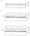
はじめに、(110)面を主表面として有する単結晶半導体基板200を用意する。そして、単結晶半導体基板200にイオンを照射して、その主表面から所定の深さにイオンを導入し、脆化層202及び単結晶半導体層204を形成する(図2(A)参照)。脆化層202の形成方法としては、半導体層への不純物元素の添加に用いられる方法(以下、イオンドーピング法という)や、イオン化したガスを質量分離して選択的に半導体層に注入する方法(以下、イオン注入法という)等が挙げられる。イオンの照射は、形成される単結晶半導体層204の厚さを考慮して行えば良い。該単結晶半導体層204の厚さは5nm乃至500nm程度とすればよく、10nm乃至200nmの厚さとするとより好ましい。イオンを照射する際の加速電圧は上記の厚さを考慮して決定することができる。
First, a single
単結晶半導体基板200は、(110)面を主表面に有する単結晶半導体基板であれば特に限られない。なお、絶縁層と単結晶半導体層との密着性や、単結晶半導体層の平坦性の効果に主眼をおく場合には、結晶面を形成する原子数が多い面を主表面として有する単結晶半導体基板を用いればよい。この意味において、本明細書中の「(110)面」との記載を、例えば、「他の結晶面(例えば(100)面)と比較して原子数の多い結晶面」と読み替えても良い。
Single
照射するイオンとしては、フッ素に代表されるハロゲンや、水素、ヘリウム等のイオンが挙げられる。ハロゲンのイオンとしてフッ素イオンを照射する場合には、原料ガスとしてBF3を用いれば良い。たとえば、単結晶半導体基板200として単結晶シリコン基板を用いて、該単結晶シリコン基板にフッ素イオンのようなハロゲンイオンを導入した場合には、脆化層202には微小な空洞が形成される。これは、導入されたハロゲンイオンがシリコン結晶格子内のシリコン原子を追い出すためと考えられている。このようにして形成された微小な空洞の体積を変化させることにより、単結晶シリコン基板を分離(劈開)させることができる。具体的には、低温の熱処理によって微小な空洞の体積変化を誘起する。なお、フッ素イオンを照射した後に、水素イオンを照射して空洞内に水素を含ませるようにしても良い。
Examples of ions to be irradiated include halogens represented by fluorine, ions of hydrogen, helium, and the like. In the case of irradiation with fluorine ions as halogen ions, BF 3 may be used as a source gas. For example, when a single crystal silicon substrate is used as the single
また、同一の原子から成り、質量数の異なる複数のイオンを照射してもよい。例えば、水素イオンを照射する場合には、H+、H2 +、H3 +イオンを含ませると共に、H3 +イオンの割合を高めておくと良い。H3 +イオンの割合を高めることで照射効率を高めることができるため、照射時間を短縮することができる。なお、単結晶半導体基板200の(110)面を用いる場合には、他の結晶面と比較して原子数が多いので平坦な分離面を得ることができる。
Moreover, you may irradiate several ion which consists of the same atoms and from which mass number differs. For example, in the case of irradiation with hydrogen ions, it is preferable to include H + , H 2 + , and H 3 + ions and to increase the ratio of H 3 + ions. Since the irradiation efficiency can be increased by increasing the ratio of H 3 + ions, the irradiation time can be shortened. Note that in the case where the (110) plane of the single
例えば、原料として水素ガスを用いたイオンドーピング法において、加速電圧が40kVの条件により、2.2×10¹⁶ions/cm2程度のイオンを照射することができる。加速電圧は30kV乃至80kV程度とすることが好ましく、この場合には、1.8×1016ions/cm2乃至4.0×1016ions/cm2程度のイオンを照射することができる。 For example, in an ion doping method using hydrogen gas as a raw material, ions of about 2.2 × 10 16 ions / cm 2 can be irradiated under an acceleration voltage of 40 kV. The acceleration voltage is preferably about 30 kV to 80 kV. In this case, ions of about 1.8 × 10 16 ions / cm 2 to 4.0 × 10 16 ions / cm 2 can be irradiated.
なお、(110)面に対して脆化層を形成する場合には、イオンのチャネリングにより濃度分布が広がりやすいため、単結晶半導体基板を水平方向から7°±5°程度傾けてイオンを照射することが好適である。水平方向に対して角度を持たせた単結晶半導体基板に対してイオン照射を行うことにより、濃度分布の分散を小さくすることができるためである。 Note that in the case where an embrittlement layer is formed with respect to the (110) plane, the concentration distribution is easily widened by ion channeling. Therefore, the single crystal semiconductor substrate is irradiated with ions inclined by about 7 ° ± 5 ° from the horizontal direction. Is preferred. This is because dispersion of the concentration distribution can be reduced by performing ion irradiation on the single crystal semiconductor substrate having an angle with respect to the horizontal direction.
なお、単結晶半導体層204と、後に形成する絶縁層との界面における欠陥(すなわち界面準位)を低減する必要がある場合には、例えば、界面となる単結晶半導体層204の表面にプラズマ処理を行えばよい。具体的には、水素雰囲気下、酸素雰囲気下、又は酸素と水素の混合雰囲気下にてプラズマ処理を行う。水素雰囲気下にてプラズマ処理を行うことにより、表面をエッチングし、汚染物を除去することができる。また、単結晶半導体層204の表面の一部を除去し、内部の密な領域を表出させることができる。また、水素により単結晶半導体層中のダングリングボンドを終端することができる。また、酸素雰囲気下においてプラズマ処理を行うことにより、表面に密な酸化膜を形成することができる。すなわち、これらの雰囲気下においてプラズマ処理を行うことにより、単結晶半導体層204と後に形成される絶縁層との界面を清浄に保ち、欠陥を低減することができる。なお、上記の雰囲気に希ガス元素を加えても、同様の効果を得ることができる。
Note that in the case where defects (that is, interface states) at the interface between the single
なお、界面の欠陥を低減する方法としては、熱酸化法による酸化膜の形成という方法も考えられる。しかしながら、熱酸化に必要な高温条件はスマートカット法には適していない。スマートカット法は、加熱処理により単結晶半導体層の分離を行うものであるが、該加熱の温度条件は400℃以上600℃以下程度と比較的低温である。一方、熱酸化に必要な温度条件は800℃以上であり、スマートカット法においてこのような高温プロセスを採用した場合には、単結晶半導体層204の分離が進行してしまうのである。以上のような理由から、スマートカット法における界面の欠陥低減にはプラズマ処理が好適であることが分かる。
As a method for reducing defects at the interface, a method of forming an oxide film by a thermal oxidation method is also conceivable. However, the high temperature conditions required for thermal oxidation are not suitable for the smart cut method. The smart cut method is a method in which a single crystal semiconductor layer is separated by heat treatment, and the temperature condition of the heating is a relatively low temperature of about 400 ° C. to 600 ° C. On the other hand, the temperature condition necessary for thermal oxidation is 800 ° C. or higher, and when such a high temperature process is adopted in the smart cut method, the separation of the single
なお、上記のプラズマ処理としては、高周波(マイクロ波等)を用いて高密度(好ましくは1×1011cm−3以上1×1013cm−3以下)且つ低電子温度(0.2eV以上2.0eV以下(より好ましくは0.5eV以上1.5eV以下))の条件下で行うプラズマ処理(以下「高密度プラズマ処理」という)が好ましい。低電子温度が特徴である高密度プラズマ処理は、活性種の運動エネルギーが低いため、通常のプラズマ処理に比べてプラズマによるダメージが少ない。このため、通常のプラズマ処理に比べて、一層良質な界面を形成することができる。なお、高密度プラズマ処理においては、水素と希ガス(ヘリウム、ネオン、アルゴン、クリプトン、キセノン等)の混合雰囲気、又は酸素と水素と希ガスの混合雰囲気とすることが好ましい。 Note that as the above plasma treatment, a high frequency (preferably 1 × 10 11 cm −3 or higher and 1 × 10 13 cm −3 or lower) and a low electron temperature (0.2 eV or higher 2 A plasma treatment (hereinafter referred to as “high density plasma treatment”) performed under a condition of 0.0 eV or less (more preferably 0.5 eV or more and 1.5 eV or less) is preferable. The high-density plasma treatment characterized by a low electron temperature is less damaged by the plasma than the normal plasma treatment because the kinetic energy of the active species is low. For this reason, it is possible to form a higher quality interface as compared with normal plasma processing. Note that in the high-density plasma treatment, a mixed atmosphere of hydrogen and a rare gas (such as helium, neon, argon, krypton, or xenon) or a mixed atmosphere of oxygen, hydrogen, and a rare gas is preferable.
なお、本実施の形態においては、プラズマ処理として、水素又は酸素を少なくとも有する雰囲気において行うものを挙げたが、本発明はこれに限定して解釈されない。例えば、酸化窒素、アンモニア、窒素等を含む雰囲気下、又はこれらと水素、酸素、希ガス等の混合雰囲気下において行っても良い。 Note that although the plasma treatment is performed in an atmosphere having at least hydrogen or oxygen in this embodiment, the present invention is not construed as being limited thereto. For example, the reaction may be performed in an atmosphere containing nitrogen oxide, ammonia, nitrogen, or the like, or a mixed atmosphere of hydrogen, oxygen, rare gas, and the like.
次に、単結晶半導体層204上に、接合層として機能する絶縁層206を形成する(図2(B)参照)。絶縁層206としては、酸化シリコン膜を、有機シランガスを用いて化学気相成長法(CVD法)により形成すると良い。その他に、シランガスを用いて化学気相成長法により作製される酸化シリコン膜を適用することもできる。化学気相成長法を用いる場合には、脆化層202から脱ガスが起こらない温度条件で成膜する必要がある。なお、単結晶半導体基板200から単結晶半導体層204を分離させるための熱処理には、成膜温度よりも高い温度が適用される。
Next, an insulating
なお、有機シランガスとしては、珪酸エチル(TEOS)、トリメチルシラン、テトラメチルシラン、テトラメチルシクロテトラシロキサン(TMCTS)、オクタメチルシクロテトラシロキサン(OMCTS)、ヘキサメチルジシラザン(HMDS)、トリエトキシシラン、トリスジメチルアミノシラン等を用いることができる。 As the organic silane gas, ethyl silicate (TEOS), trimethylsilane, tetramethylsilane, tetramethylcyclotetrasiloxane (TMCTS), octamethylcyclotetrasiloxane (OMCTS), hexamethyldisilazane (HMDS), triethoxysilane, Trisdimethylaminosilane or the like can be used.
また、絶縁層206としては、モノシランと二酸化窒素を原料ガスとして用いて、LPCVD法により酸化窒化シリコン膜を形成してもよい。これにより、300℃以上400℃以下の低温条件においても、良質な絶縁層206を形成することができる。例えば、モノシランの流量が40sccm、二酸化窒素の流量が400sccm、圧力が266.6Pa、温度が350℃の条件において良好な絶縁層を形成することが可能である。
As the insulating
上記絶縁層206は、5nm乃至500nm程度の厚さで設けられる。前述の厚さとすることにより、被形成表面を平滑化すると共に、絶縁層206の成長表面の平滑性を確保することが可能である。また、接合する基板との歪みを緩和することができる。なお、後の絶縁表面を有する基板にも同様の絶縁層を設けておくことができる。このように、接合を形成する面の一方又は双方を、有機シランを原材料として成膜した酸化シリコン膜とすることで、接合を非常に強固なものとすることができる。
The insulating
なお、単結晶半導体層204と絶縁層206の間に窒素含有絶縁層を設ける構成としてもよい。窒素含有絶縁層は窒化シリコン、窒化酸化シリコン又は酸化窒化シリコン等を用いて形成することができる。なお、窒素含有絶縁層は単層構造でも良いし積層構造でも良い。例えば、単結晶半導体層204側から酸化窒化シリコン膜と窒化酸化シリコン膜を積層して窒素含有絶縁層とすることができる。窒素含有絶縁層は、アルカリ金属、アルカリ土類金属のような可動イオンや水分等の不純物が単結晶半導体層204に侵入することを防ぐために設けられる。なお、不純物の侵入を防ぐことができるのであれば、窒素含有絶縁層以外の絶縁層を設けても良い。また、窒素含有絶縁層を設ける場合には、絶縁層206と窒素含有絶縁層を合わせて絶縁層と呼ぶこともできる。
Note that a nitrogen-containing insulating layer may be provided between the single
ここで、酸化窒化シリコンとは、その組成において、窒素よりも酸素の含有量が多いものを示し、例えば、酸素が50原子%以上70原子%以下、窒素が0.5原子%以上15原子%以下、珪素が25原子%以上35原子%以下、水素が0.1原子%以上10原子%以下の範囲で含まれるものをいう。また、窒化酸化シリコンとは、その組成において、酸素よりも窒素の含有量が多いものを示し、例えば、酸素が5原子%以上30原子%以下、窒素が20原子%以上55原子%以下、珪素が25原子%以上35原子%以下、水素が10原子%以上30原子%以下の範囲で含まれるものをいう。但し、上記範囲は、ラザフォード後方散乱法(RBS:Rutherford Backscattering Spectrometry)や、水素前方散乱法(HFS:Hydrogen Forward Scattering)を用いて測定した場合のものである。また、構成元素の含有比率は、その合計が100原子%を超えない値をとる。 Here, silicon oxynitride indicates a composition having a higher oxygen content than nitrogen. For example, oxygen is 50 atomic% to 70 atomic%, and nitrogen is 0.5 atomic% to 15 atomic%. Hereinafter, silicon is contained in the range of 25 atomic% to 35 atomic% and hydrogen in the range of 0.1 atomic% to 10 atomic%. Silicon nitride oxide refers to a composition having a nitrogen content higher than that of oxygen. For example, oxygen is 5 atomic% to 30 atomic%, nitrogen is 20 atomic% to 55 atomic%, silicon In the range of 25 atomic% to 35 atomic% and hydrogen in the range of 10 atomic% to 30 atomic%. However, the above ranges are those measured using Rutherford Backscattering Spectrometry (RBS) or Hydrogen Forward Scattering (HFS). Further, the content ratio of the constituent elements takes a value that the total does not exceed 100 atomic%.
次に、絶縁表面を有する基板210と、絶縁層206とを密接させる(図2(C)参照)。絶縁表面を有する基板210と絶縁層206とを密接させて圧力をかけることで、強固な接合を形成することが可能である。なお、絶縁層206を介して絶縁表面を有する基板210と単結晶半導体基板200を貼り合わせた後には、加熱処理を行うことが好ましい。加熱処理を行うことで接合強度をさらに向上させることができる。
Next, the
良好な接合を形成するために、接合が形成される表面を活性化しておいても良い。例えば、接合を形成する面に原子ビーム又はイオンビームを照射する。原子ビーム又はイオンビームを利用する場合には、アルゴン等の不活性ガス原子ビーム又は不活性ガスイオンビームを用いることができる。その他に、プラズマ処理やラジカル処理を行っても良い。このような表面処理により、200℃乃至400℃程度の低温で異種材料間の接合を形成することができる。 In order to form a good bond, the surface on which the bond is formed may be activated. For example, an atomic beam or an ion beam is irradiated to the surface on which the junction is formed. When an atomic beam or an ion beam is used, an inert gas atom beam such as argon or an inert gas ion beam can be used. In addition, plasma treatment or radical treatment may be performed. By such surface treatment, a bond between different materials can be formed at a low temperature of about 200 ° C. to 400 ° C.
なお、絶縁表面を有する基板210としては、アルミノシリケートガラス、アルミノホウケイ酸ガラス、バリウムホウケイ酸ガラスのような電子工業用に使われる各種ガラス基板、石英基板、セラミック基板、サファイヤ基板等を用いることができる。中でもガラス基板を用いるのが好ましく、例えば第6世代(1500mm×1850mm)、第7世代(1870mm×2200mm)、第8世代(2200mm×2400mm)といわれる大面積のマザーガラス基板を用いることもできる。大面積のマザーガラス基板を、絶縁表面を有する基板210として用いることで、半導体基板の大面積化が実現できる。なお、絶縁表面を有する基板210は上記の基板に限定されるものではない。例えば、耐熱温度が許せば樹脂材料からなる基板を用いることも可能である。本実施の形態の作製方法においては、高温プロセスが不要であるため、耐熱温度が低い基板を用いることが可能となっている。
As the
また、絶縁表面を有する基板210上にバリア層として機能する絶縁層を設ける構成としても良い。該絶縁層を設けることにより、単結晶半導体層204へのアルカリ金属やアルカリ土類金属のような不純物の侵入を防ぐことができる。もちろん、絶縁表面を有する基板210から単結晶半導体層204への不純物の侵入が問題とならない場合には、バリア層として機能する絶縁層を設ける必要はない。
Alternatively, an insulating layer functioning as a barrier layer may be provided over the
上記の絶縁層は、酸化シリコン、窒化シリコン、窒化酸化シリコン、酸化窒化シリコン等から選択された一又は複数の材料を用いて形成することができる。絶縁層は単層構造でも良いし積層構造でも良い。一例としては、絶縁表面を有する基板210側から、窒化シリコンと酸化シリコンとを順に積層した構成の絶縁層を用いることができる。なお、不純物の侵入を防ぐことができるのであれば、上記材料を用いて形成することに限られない。
The insulating layer can be formed using one or a plurality of materials selected from silicon oxide, silicon nitride, silicon nitride oxide, silicon oxynitride, and the like. The insulating layer may have a single layer structure or a laminated structure. As an example, an insulating layer in which silicon nitride and silicon oxide are sequentially stacked from the
次に、加熱処理を行い、脆化層202を分離面として単結晶半導体層204を単結晶半導体基板200から分離する(図2(D)参照)。例えば、400℃乃至600℃の熱処理を行うことにより、脆化層202に形成された微小な空洞内の圧力が上昇し、体積膨張を誘起して分離させることができる。絶縁層206は絶縁表面を有する基板210と接合しているので、絶縁表面を有する基板210上には単結晶半導体基板200と同様の結晶性の単結晶半導体層204が残存することとなる。
Next, heat treatment is performed so that the single
なお、上記の加熱処理前に、150℃以上350℃以下程度の温度範囲にて加熱処理を施すことにより、接合界面を強化することができる。これにより、異なる熱膨張係数を有する材料を接合させた場合であっても、接合界面からの剥離を抑制することができる。例えば、200℃、2時間の加熱処理を適用すればよい。 Note that the bonding interface can be strengthened by performing heat treatment in a temperature range of approximately 150 ° C. to 350 ° C. before the heat treatment. Thereby, even if it is a case where the material which has a different thermal expansion coefficient is joined, peeling from a joining interface can be suppressed. For example, a heat treatment at 200 ° C. for 2 hours may be applied.
絶縁表面を有する基板210としてガラス基板を用いる場合には、ガラス基板の歪み点近傍、具体的には歪み点±50℃で加熱を行えば良い。より具体的には、580℃以上680℃以下で行えばよい。該加熱処理は大気圧下で行っても良いし、減圧下で行っても良い。雰囲気についても、窒素雰囲気や、酸素雰囲気など、適宜設定することができる。なお、該加熱処理は、加熱後に収縮する性質を有する基板を用いる場合であればガラス基板に限らず適用することができる。より具体的には、200℃、2時間の加熱処理の後、600℃、2時間の加熱処理を行えばよい。
When a glass substrate is used as the
なお、ガラス基板は加熱によって収縮するという性質を有する。このため、あらかじめガラス基板を歪み点近傍、具体的には歪み点±50℃程度(若しくはそれ以上)で加熱処理後に冷却しておくと、その後の加熱処理における収縮を抑制することができる。これにより、熱膨張率の異なる単結晶半導体層を接合したガラス基板に加熱処理を行う場合であっても、ガラス基板からの単結晶半導体層の剥離を防ぐことができる。また、ガラス基板及び単結晶半導体層の反りなどの変形を防止することもできる。 Note that the glass substrate has a property of shrinking by heating. For this reason, if the glass substrate is cooled in advance near the strain point, specifically, at a strain point of about ± 50 ° C. (or higher) after the heat treatment, shrinkage in the subsequent heat treatment can be suppressed. Accordingly, even when heat treatment is performed on a glass substrate to which single crystal semiconductor layers having different thermal expansion coefficients are bonded, peeling of the single crystal semiconductor layer from the glass substrate can be prevented. In addition, deformation such as warpage of the glass substrate and the single crystal semiconductor layer can be prevented.
なお、ガラス基板を用いる場合には、加熱終了時の急速な冷却を避けることが好ましい。具体的には2℃/分以下、好ましくは1℃/分以上2℃/分以下の速度で、歪み点以下の温度まで冷却するとよい。降温速度を小さくすることにより、ガラス基板が縮む際に生じる局所的な応力を緩和することができる。 In addition, when using a glass substrate, it is preferable to avoid rapid cooling at the end of heating. Specifically, cooling to a temperature below the strain point at a rate of 2 ° C./min or less, preferably 1 ° C./min or more and 2 ° C./min or less is preferable. By reducing the temperature decrease rate, local stress generated when the glass substrate shrinks can be relaxed.
なお、接合の工程に係る加熱処理と、分離の工程に係る加熱処理とを同時に行うこともできる。この場合、1度の加熱処理で二つの工程を行うことができるため、低コストに半導体基板を作製することができる。 Note that the heat treatment related to the bonding step and the heat treatment related to the separation step can be performed simultaneously. In this case, since two steps can be performed by one heat treatment, a semiconductor substrate can be manufactured at low cost.
上記の工程によって得られた単結晶半導体層204については、その表面を平坦化するため、化学的機械的研磨(Chemical Mechanical Polishing:CMP)などを行うことが好ましい。単結晶半導体層204の平坦性を向上することにより、後に形成する半導体素子の特性のばらつきを抑えることができる。なお、所望の特性が得られるようであれば、CMP工程などは省略してもかまわない。
The single
また、再度の加熱やレーザー光の照射を行うことにより、単結晶半導体層204の特性を向上させても良い。なお、加熱処理時の温度は、絶縁表面を有する基板210の耐熱温度を目安とすることができる。絶縁表面を有する基板210としてガラス基板を用いる場合には、ガラス基板の歪み点を目安とすればよい。具体的には、歪み点±50℃(580℃以上680℃以下)程度の温度にて加熱処理を行えばよい。
Further, the characteristics of the single
レーザー光の照射には、例えば、連続発振のレーザー(CWレーザー)や、パルス発振レーザー(10Hz以上100Hz以下程度の発振周波数であることが好ましい)を用いることができる。具体的には、連続発振のレーザーとして、Arレーザー、Krレーザー、CO2レーザー、YAGレーザー、YVO4レーザー、YLFレーザー、YAlO3レーザー、GdVO4レーザー、Y2O3レーザー、ルビーレーザー、アレキサンドライトレーザー、Ti:サファイアレーザー、ヘリウムカドミウムレーザー等を用いることができる。また、パルス発振レーザーとして、Arレーザー、Krレーザー、エキシマ(ArF、KrF、XeCl)レーザー、CO2レーザー、YAGレーザー、YVO4レーザー、YLFレーザー、YAlO3レーザー、GdVO4レーザー、Y2O3レーザー、ルビーレーザー、アレキサンドライトレーザー、Ti:サファイアレーザー、銅蒸気レーザーまたは金蒸気レーザー等を用いることができる。なお、このようなパルス発振レーザーは、発振周波数を増加させると、連続発振レーザーと同等に扱うことも可能である。 For the laser light irradiation, for example, a continuous wave laser (CW laser) or a pulsed laser (preferably an oscillation frequency of about 10 Hz to 100 Hz) can be used. Specifically, as a continuous wave laser, Ar laser, Kr laser, CO 2 laser, YAG laser, YVO 4 laser, YLF laser, YAlO 3 laser, GdVO 4 laser, Y 2 O 3 laser, ruby laser, alexandrite laser Ti: sapphire laser, helium cadmium laser, or the like can be used. Also, Ar laser, Kr laser, excimer (ArF, KrF, XeCl) laser, CO 2 laser, YAG laser, YVO 4 laser, YLF laser, YAlO 3 laser, GdVO 4 laser, Y 2 O 3 laser are used as pulsed lasers. Ruby laser, alexandrite laser, Ti: sapphire laser, copper vapor laser, gold vapor laser, or the like can be used. Such a pulsed laser can be handled in the same manner as a continuous wave laser when the oscillation frequency is increased.
特に、酸素濃度が10ppm以下の低酸素濃度雰囲気下でレーザー光を照射して、少なくとも単結晶半導体層の上部を溶融させることにより、単結晶半導体層の表面を平坦化することができる。また、レーザー光照射の前、又は後に、CMP、又はエッチングを施すことにより、単結晶半導体層を所定の厚さとなるように加工することが好ましい。もちろん、レーザー光照射の前、又は後のいずれか一方に限られず、両方に上記の処理を施すこともできる。 In particular, the surface of the single crystal semiconductor layer can be planarized by irradiating laser light in a low oxygen concentration atmosphere with an oxygen concentration of 10 ppm or less to melt at least the upper portion of the single crystal semiconductor layer. Further, it is preferable that the single crystal semiconductor layer be processed to have a predetermined thickness by performing CMP or etching before or after laser light irradiation. Of course, it is not limited to either before or after laser light irradiation, and the above-described treatment can be performed on both.
次に、絶縁表面を有する基板210側に接合層として機能する絶縁層206を設ける場合について、図3を用いて説明する。なお、脆化層202の作製工程については図2に示す場合と同様であるため、詳細については省略する。プラズマ処理を行う場合にも、上記を参照すればよい。
Next, the case where the insulating
脆化層202を形成した後に(図3(A)参照)、絶縁表面を有する基板210上に形成された、接合層として機能する絶縁層206と、単結晶半導体層204とを密着させ、接合させる(図3(B)参照)。なお、絶縁表面を有する基板210上にバリア層として機能する絶縁層を形成した後に、絶縁層206を形成する構成としても良い。バリア層として機能する絶縁層を設けることにより、単結晶半導体層204へのアルカリ金属やアルカリ土類金属のような不純物の侵入を防ぐことができる。もちろん、絶縁表面を有する基板210から単結晶半導体層204への不純物の侵入が問題とならない場合には、バリア層として機能する絶縁層を設ける必要はない。
After the
上記のバリア層として機能する絶縁層は、酸化シリコン、窒化シリコン、窒化酸化シリコン、酸化窒化シリコン等から選択された一又は複数の材料を用いて形成することができる。絶縁層は単層構造でも良いし積層構造でも良い。一例としては、絶縁表面を有する基板210側から、窒化シリコンと酸化シリコンとを順に積層した構成の絶縁層を用いることができる。なお、不純物の侵入を防ぐことができるのであれば、上記材料を用いて形成することに限られない。
The insulating layer functioning as the barrier layer can be formed using one or a plurality of materials selected from silicon oxide, silicon nitride, silicon nitride oxide, silicon oxynitride, and the like. The insulating layer may have a single layer structure or a laminated structure. As an example, an insulating layer in which silicon nitride and silicon oxide are sequentially stacked from the
その後、単結晶半導体基板200を分離させる(図3(C)参照)。単結晶半導体基板200を分離させる際の熱処理は、図2(D)の場合と同様にして行うことができるため、詳細については省略する。このようにして、図3(C)に示す半導体基板を得ることができる。
After that, the single
図3(C)に示す半導体基板に対しても、化学的機械的研磨(Chemical Mechanical Polishing:CMP)などを行うことが好ましい。単結晶半導体層204の平坦性を向上させることにより、後に形成する半導体素子の特性のばらつきを抑えることができる。なお、所望の特性が得られるようであれば、CMP工程などは省略してもかまわない。
Also for the semiconductor substrate shown in FIG. 3C, chemical mechanical polishing (CMP) or the like is preferably performed. By improving the flatness of the single
また、再度の加熱やレーザー光の照射を行うことにより、単結晶半導体層204の特性を向上させても良い。加熱処理時の温度や用いることができるレーザーについては、上記を参照できるため、ここでは省略する。
Further, the characteristics of the single
以上により、(110)面を主表面とする単結晶半導体層を有する半導体基板を提供することができる。(110)面における原子の面密度は、他の結晶面と比較して大きいため、絶縁層と単結晶半導体層との密着性が向上する。すなわち、単結晶半導体層の剥離を抑制することができる。 As described above, a semiconductor substrate having a single crystal semiconductor layer having a (110) plane as a main surface can be provided. Since the surface density of atoms in the (110) plane is higher than that of other crystal planes, adhesion between the insulating layer and the single crystal semiconductor layer is improved. That is, separation of the single crystal semiconductor layer can be suppressed.
また、(110)面では上記のように原子が密に配列しているため、その他の面を用いる場合と比較して、作製したSOI基板における単結晶半導体層の平坦性が向上する。すなわち、該単結晶半導体層を用いて作製したトランジスタは優れた特性を有することになる。 Further, since the atoms are densely arranged on the (110) plane as described above, the flatness of the single crystal semiconductor layer in the manufactured SOI substrate is improved as compared with the case of using other planes. That is, a transistor manufactured using the single crystal semiconductor layer has excellent characteristics.
なお、単結晶半導体層と、絶縁層との界面における欠陥を低減する必要がある場合には、単結晶半導体層の表面にプラズマ処理を行えばよい。これにより、極めて高品質な半導体基板を提供することが可能となる。 Note that in the case where defects at the interface between the single crystal semiconductor layer and the insulating layer need to be reduced, plasma treatment may be performed on the surface of the single crystal semiconductor layer. This makes it possible to provide an extremely high quality semiconductor substrate.
(実施の形態2)
本実施の形態では、本発明の半導体装置の製造方法の別の一例について、図4及び5を参照して説明する。なお、本実施の形態では、イオン照射時における単結晶半導体層のダメージを低減することが可能な半導体基板の製造方法について説明する。また、図4を用いて単結晶半導体基板側に接合層として機能する絶縁層を設ける場合について説明し、図5を用いて絶縁表面を有する基板側に接合層として機能する絶縁層を設ける場合について説明する。
(Embodiment 2)
In this embodiment, another example of the method for manufacturing a semiconductor device of the present invention will be described with reference to FIGS. Note that in this embodiment, a method for manufacturing a semiconductor substrate capable of reducing damage to a single crystal semiconductor layer during ion irradiation will be described. In addition, the case where an insulating layer functioning as a bonding layer is provided on the single crystal semiconductor substrate side will be described with reference to FIG. 4, and the case where an insulating layer functioning as a bonding layer is provided on the substrate side having an insulating surface will be described with reference to FIG. explain.
はじめに、(110)面を主表面として有する単結晶半導体基板400を用意する。そして、単結晶半導体基板400上に保護層として機能する絶縁層450を形成する(図4(A)参照)。単結晶半導体基板の詳細については実施の形態1を参照することができるため、ここでは省略する。
First, a single
絶縁層450は、酸化シリコン、窒化シリコン、窒化酸化シリコン、酸化窒化シリコン等から選択された一又は複数の材料を用いて形成することができる。絶縁層450は単層構造でも良いし積層構造でも良い。絶縁層450の形成方法としては、化学気相成長法(CVD法)やスパッタ法、熱酸化法、熱窒化法等が挙げられるが、特にこれに限られるものではない。例えば、熱酸化法を用いる場合には、HClを1体積%以上10体積%以下程度含む雰囲気で形成された熱酸化膜を絶縁層450として用いると良い。厚さは10nm乃至200nm程度とすることが好ましい。絶縁層450を設けることにより、イオンの照射による単結晶半導体基板400の表面(後の単結晶半導体層の表面)の荒れを防止できる。
The insulating
次に、絶縁層450を介して、単結晶半導体基板400の表面から所定の深さにイオンを導入し、脆化層402及び単結晶半導体層404を形成する(図4(B)参照)。脆化層402及び単結晶半導体層404の作製方法の詳細については実施の形態1を参照できるため、ここでは省略する。脆化層402の形成後には、絶縁層450を除去しても良いが、絶縁層450を残存させた場合には下地絶縁層として機能させることが可能である。このため、絶縁層450は除去しないことが好ましい。絶縁層450を有することにより、アルカリ金属、アルカリ土類金属のような可動イオンや水分等の不純物が単結晶半導体層404に侵入することを防止できる。特に、窒化酸化シリコンや、窒化シリコンを用いる場合には、不純物の単結晶半導体層への侵入を効果的に防ぐことができる。例えば、単結晶半導体基板側から酸化窒化シリコン膜を50nm、窒化酸化シリコン膜を50nmの厚さで順に積層して形成することができる。この場合には、加速電圧が40kVの条件により、2.2×10¹⁶ions/cm2程度のイオンを照射すればよい。又は、PECVD法を用いて、単結晶半導体基板側から酸化窒化シリコン膜と窒化酸化シリコン膜をそれぞれ50nm形成し、加速電圧を35kV程度、イオンドーズ量を2.9×1016ions/cm2程度とした高周波放電イオンドーピング法を用いて、H+、H2 +、H3 +イオンを照射しても良い。なお、この場合、分離後の単結晶半導体層の厚さは120nm程度となる。
Next, ions are introduced to a predetermined depth from the surface of the single
絶縁層450の作製方法としては、上記以外にも、例えば、オゾン水や過酸化水素水を用いて、単結晶半導体基板400の表面に酸化膜を形成する方法などがある。また、オゾン雰囲気に晒すことにより、単結晶半導体基板400の表面に酸化膜を形成しても良い。なお、オゾン雰囲気は、酸素雰囲気に紫外光を照射することで実現できる。また、N2O及びO2雰囲気におけるプラズマ処理、N2及びO2雰囲気におけるプラズマ処理、N2O及びNH3雰囲気におけるプラズマ処理、O2雰囲気におけるプラズマ処理、N2、O2及びH2雰囲気におけるプラズマ処理を施すことにより、酸化膜を形成することもできる。なお、この場合において、酸化膜の厚さは0.5nm乃至3nm程度である。また、脆化層の形成後には、酸化窒化シリコンや窒化酸化シリコン等を積層することもできる。
As a method for manufacturing the insulating
次に、絶縁層450上に、接合層として機能する絶縁層406を形成する(図4(C)参照)。絶縁層406は、酸化シリコン膜を、有機シランガスを用い化学気相成長法(CVD法)により形成すると良い。その他に、シランガスを用いて化学気相成長法により作製される酸化シリコン膜を適用することもできる。化学気相成長法を用いる場合には、脆化層402から脱ガスが起こらない温度条件で成膜する必要がある。なお、単結晶半導体基板400から単結晶半導体層404を分離する熱処理には、成膜温度よりも高い温度が適用される。
Next, an insulating
絶縁層406の作製方法等の詳細については、実施の形態1を参照することができるため、ここでは省略する。
The details of the manufacturing method and the like of the insulating
次に、絶縁表面を有する基板410と、絶縁層406とを密接させる(図4(D)参照)。絶縁表面を有する基板410と絶縁層406とを密接させて圧力をかけることで、強固な接合を形成することが可能である。なお、絶縁層406を介して絶縁表面を有する基板410と単結晶半導体基板400を貼り合わせた後には、加熱処理を行うことが好ましい。加熱処理を行うことで接合強度をさらに向上させることができる。
Next, the
良好な接合を形成するために、接合が形成される表面を活性化しておいても良い。例えば、接合を形成する面に原子ビーム若しくはイオンビームを照射する。原子ビーム若しくはイオンビームを利用する場合には、アルゴン等の不活性ガス原子ビーム若しくは不活性ガスイオンビームを用いることができる。その他に、プラズマ処理若しくはラジカル処理を行う。このような表面処理により、200℃乃至400℃程度の低温で異種材料間の接合を形成することができる。 In order to form a good bond, the surface on which the bond is formed may be activated. For example, an atomic beam or an ion beam is irradiated to the surface on which the junction is formed. When an atomic beam or an ion beam is used, an inert gas atom beam or inert gas ion beam such as argon can be used. In addition, plasma treatment or radical treatment is performed. By such surface treatment, a bond between different materials can be formed at a low temperature of about 200 ° C. to 400 ° C.
なお、絶縁表面を有する基板410としては、アルミノシリケートガラス、アルミノホウケイ酸ガラス、バリウムホウケイ酸ガラスのような電子工業用に使われる各種ガラス基板、石英基板、セラミック基板、サファイヤ基板等を用いることができる。好ましくはガラス基板を用いるのがよく、例えば第6世代(1500mm×1850mm)、第7世代(1870mm×2200mm)、第8世代(2200mm×2400mm)といわれる大面積のマザーガラス基板を用いることもできる。大面積のマザーガラス基板を、絶縁表面を有する基板410として用いることで、半導体基板の大面積化が実現できる。なお、絶縁表面を有する基板410は上記の基板に限定されるものではない。例えば、耐熱温度が許せば樹脂材料からなる基板を用いることも可能である。本実施の形態の作製方法においては、高温プロセスが不要であるため、耐熱温度が低い基板を用いることが可能となっている。
Note that as the
次に、加熱処理を行い、脆化層402を分離面として単結晶半導体層404を単結晶半導体基板400から分離する(図4(E)参照)。例えば、400℃乃至600℃の熱処理を行うことにより、脆化層402に形成された微小な空洞の体積変化を誘起して分離させることができる。絶縁層406は絶縁表面を有する基板410と接合しているので、絶縁表面を有する基板410上には単結晶半導体基板400と同じ結晶性の単結晶半導体層404が残存することとなる。
Next, heat treatment is performed so that the single
分離における加熱処理の詳細については、実施の形態1を参照することができる。なお、接合の工程に係る加熱処理と、分離の工程に係る加熱処理とを同時に行うこともできる。この場合、1度の加熱処理で二つの工程を行うことができるため、低コストに半導体基板を作製することができる。
上記の工程によって得られた単結晶半導体層404については、その表面を平坦化するため、化学的機械的研磨(Chemical Mechanical Polishing:CMP)などを行うことが好ましい。単結晶半導体層404の平坦性を向上することにより、後に形成する半導体素子の特性のばらつきを抑えることができる。なお、所望の特性が得られるようであれば、CMP工程などは省略してもかまわない。
The single
また、再度の加熱やレーザー光の照射を行うことにより、単結晶半導体層404の特性を向上させても良い。なお、加熱処理時の温度や、用いるレーザーに関しては、実施の形態1を参照することができる。
Further, the characteristics of the single
次に、絶縁表面を有する基板410側に接合層として機能する絶縁層406を設ける場合について、図5を用いて説明する。なお、脆化層402の作製に係る工程までは図4に示す場合と同様であるため、詳細については省略する。
Next, the case where the insulating
脆化層402を形成した後に(図5(A)参照)、絶縁表面を有する基板410上に形成された、接合層として機能する絶縁層406と、絶縁層450とを密着させ、接合させる(図5(B)参照)。なお、絶縁表面を有する基板410上にバリア層として機能する絶縁層を形成した後に、絶縁層406を形成する構成としても良い。バリア層として機能する絶縁層を設けることにより、単結晶半導体層404へのアルカリ金属やアルカリ土類金属のような不純物の侵入を防ぐことができる。もちろん、絶縁表面を有する基板410から単結晶半導体層404への不純物の侵入が問題とならない場合には、バリア層として機能する絶縁層を設ける必要はない。
After the
上記のバリア層として機能する絶縁層は、酸化シリコン、窒化シリコン、窒化酸化シリコン、酸化窒化シリコン等から選択された一又は複数の材料を用いて形成することができる。絶縁層は単層構造でも良いし積層構造でも良い。一例としては、絶縁表面を有する基板410側から、窒化シリコンと酸化シリコンとを順に積層した構成の絶縁層を用いることができる。なお、不純物の侵入を防ぐことができるのであれば、上記材料を用いて形成することに限られない。
The insulating layer functioning as the barrier layer can be formed using one or a plurality of materials selected from silicon oxide, silicon nitride, silicon nitride oxide, silicon oxynitride, and the like. The insulating layer may have a single layer structure or a laminated structure. As an example, an insulating layer in which silicon nitride and silicon oxide are sequentially stacked from the
その後、単結晶半導体基板400を分離させる(図5(C)参照)。単結晶半導体基板400を分離させる際の熱処理は、実施の形態1を参照できるため、詳細については省略する。このようにして、図5(C)に示す半導体基板を得ることができる。
After that, the single
図5(C)に示す半導体基板に対しても、化学的機械的研磨(Chemical Mechanical Polishing:CMP)などを行うことが好ましい。単結晶半導体層404の平坦性を向上させることにより、後に形成する半導体素子の特性のばらつきを抑えることができる。なお、所望の特性が得られるようであれば、CMP工程などは省略してもかまわない。
It is preferable to perform chemical mechanical polishing (CMP) or the like on the semiconductor substrate illustrated in FIG. By improving the flatness of the single
また、再度の加熱やレーザー光の照射を行うことにより、単結晶半導体層404の特性を向上させても良い。加熱処理時の温度や用いることができるレーザーについても、実施の形態1を参照できるため、ここでは省略する。
Further, the characteristics of the single
以上により、(110)面を主表面とする単結晶半導体層を有する半導体基板を提供することができる。(110)面における原子の面密度は、他の結晶面と比較して大きいため、絶縁層と単結晶半導体層との密着性が向上する。すなわち、単結晶半導体層の剥離を抑制することができる。 As described above, a semiconductor substrate having a single crystal semiconductor layer having a (110) plane as a main surface can be provided. Since the surface density of atoms in the (110) plane is higher than that of other crystal planes, adhesion between the insulating layer and the single crystal semiconductor layer is improved. That is, separation of the single crystal semiconductor layer can be suppressed.
また、(110)面では上記のように原子が密に配列しているため、その他の面を用いる場合と比較して、作製したSOI基板における単結晶半導体層の平坦性が向上する。すなわち、該単結晶半導体層を用いて作製したトランジスタは優れた特性を有することになる。 Further, since the atoms are densely arranged on the (110) plane as described above, the flatness of the single crystal semiconductor layer in the manufactured SOI substrate is improved as compared with the case of using other planes. That is, a transistor manufactured using the single crystal semiconductor layer has excellent characteristics.
なお、本実施の形態においては、絶縁層450を設けることにより、イオン照射の際の単結晶半導体層404へのダメージを低減している。これにより、欠陥の数自体を低減することができるため、半導体素子の特性をより一層高めることができる。
Note that in this embodiment, the insulating
本実施の形態は、実施の形態1と適宜組み合わせて用いることができる。
This embodiment can be combined with
(実施の形態3)
本実施の形態では、実施の形態1又は2において作製した半導体基板を用いて半導体装置を製造する方法の一例について、図6乃至9を参照して説明する。なお、本実施の形態においては、nチャネル型トランジスタとpチャネル型トランジスタとを用いた半導体装置の一例として、相補型半導体装置(いわゆるCMOS)を例に挙げて説明することにする。
(Embodiment 3)
In this embodiment, an example of a method for manufacturing a semiconductor device using the semiconductor substrate manufactured in
図6は、実施の形態1において作製された半導体基板の平面図である。絶縁表面を有する基板600上に、(110)面を主表面として有する単結晶半導体層602が設けられている。ここで、図6(A)は円形の単結晶半導体基板を用いて単結晶半導体層602を形成した場合を示しており、図6(B)は矩形の単結晶半導体基板を用いて単結晶半導体層602を形成した場合を示している。図6(A)のように円形の単結晶半導体基板を用いる場合には、単結晶半導体基板を加工する必要がないため好ましい。図6(B)のように矩形の単結晶半導体基板を用いる場合には、複数の単結晶半導体層をマトリクス状に配列して、大面積の基板を得ることができる点で有利である。なお、図6(A)において、円形の単結晶半導体層602の一部が欠けた形状となっているが、これはオリエンテーションフラット(OF)である。図6(B)の場合には、オリエンテーションフラットは<110>軸に平行な方向に配置されている。
FIG. 6 is a plan view of the semiconductor substrate manufactured in the first embodiment. A single
一般に、nチャネル型トランジスタとpチャネル型トランジスタとでは、pチャネル型トランジスタの移動度が小さい。このため、同等の電流駆動能力(又は高速動作)を実現するためには、pチャネル型トランジスタのチャネル幅を相対的に大きくしなくてはならない。ここで、nチャネル型トランジスタとpチャネル型トランジスタを共に用いる場合には、pチャネル型トランジスタの大きさは、レイアウトを最適化する際の障害となる。レイアウトを最適化して回路面積を縮小するためには、nチャネル型トランジスタとpチャネル型トランジスタの大きさが概ね同等であることが求められる。 In general, an n-channel transistor and a p-channel transistor have a low mobility of the p-channel transistor. For this reason, in order to realize equivalent current driving capability (or high-speed operation), the channel width of the p-channel transistor must be relatively increased. Here, when both an n-channel transistor and a p-channel transistor are used, the size of the p-channel transistor becomes an obstacle when optimizing the layout. In order to reduce the circuit area by optimizing the layout, the n-channel transistor and the p-channel transistor are required to be approximately equal in size.
本発明では、(110)面を主表面とする単結晶半導体層602を用い、さらに、トランジスタのチャネル長方向を<110>軸方向にとることにより、pチャネル型トランジスタの移動度を最大限に引き出している。ここで、チャネル長方向とは、トランジスタにおいてキャリアが流れる方向いうものとする。この場合、nチャネル型トランジスタの移動度は幾分犠牲になるが、レイアウトの最適化の観点からは、むしろ好ましいと言える。nチャネル型トランジスタとpチャネル型トランジスタの大きさをより近づけることができるためである。
In the present invention, the mobility of the p-channel transistor is maximized by using the single
例えば、nチャネル型トランジスタのチャネル長方向を<100>軸方向にとった場合には、<110>軸方向とした場合と比較して移動度は大きくなるが、この場合には、pチャネル型トランジスタと直交することになってしまう。つまり、レイアウト上は非常に不利になってしまう。nチャネル型トランジスタとpチャネル型トランジスタのチャネル長方向を<110>軸方向とすることで、このような問題を解消し、レイアウトを最適化することができる。 For example, when the channel length direction of an n-channel transistor is in the <100> axis direction, the mobility is higher than in the <110> axis direction. It will be orthogonal to the transistor. In other words, the layout is very disadvantageous. By setting the channel length direction of the n-channel transistor and the p-channel transistor to the <110> axis direction, such a problem can be solved and the layout can be optimized.
なお、pチャネル型トランジスタの移動度は、(110)面を主表面とする単結晶半導体層を用いて、チャネル長方向を<110>軸方向とした場合(以下、「(110)面<110>軸」と記す。他の条件についても同様)が最大であり、(110)面<100>軸、(100)面<110>軸、(100)面<100>軸の順に低下してゆく。一方、nチャネル型トランジスタの移動度は、pチャネル型トランジスタとは反対の傾向となり、(100)面<100>軸、(100)面<110>軸、(110)面<100>軸、(110)面<110>軸の順である。 Note that the mobility of a p-channel transistor is as follows when a single crystal semiconductor layer having a (110) plane as a main surface is used and the channel length direction is set to the <110> axis direction (hereinafter referred to as “(110) plane <110 The same is true for other conditions), and decreases in the order of (110) plane <100> axis, (100) plane <110> axis, and (100) plane <100> axis. . On the other hand, the mobility of the n-channel transistor tends to be opposite to that of the p-channel transistor, and the (100) plane <100> axis, the (100) plane <110> axis, the (110) plane <100> axis, ( 110) The order of the plane <110> axis.
したがって、(110)面<110>軸の条件を用いることにより、pチャネル型トランジスタの移動度を最大限に引き出して、半導体装置のレイアウトを最適化し、半導体装置の小型化を実現することができる。 Therefore, by using the condition of the (110) plane <110> axis, the mobility of the p-channel transistor can be maximized, the layout of the semiconductor device can be optimized, and the semiconductor device can be downsized. .
次に、実際の製造方法について図7乃至9を参照して説明する。 Next, an actual manufacturing method will be described with reference to FIGS.
はじめに、実施の形態1に示した方法等を用いて、絶縁表面を有する基板上に、(110)面を主表面とする単結晶半導体層を形成する(図7(A)参照)。ここでは、絶縁表面を有する基板700の上に接合層として機能する絶縁層702、単結晶半導体層704を順に設けた構成を用いて説明するが、本発明はこれに限られるものではない。なお、図7に示す断面は、単結晶半導体層704の<110>軸に沿った断面である。
First, a single crystal semiconductor layer having a (110) plane as a main surface is formed over a substrate having an insulating surface by using the method described in Embodiment 1 (see FIG. 7A). Here, description is made using a structure in which an insulating
次に、単結晶半導体層704及び絶縁層702を所望の形状にパターニングして、島状の単結晶半導体層を形成する。この際、後のトランジスタのチャネル長方向が、<110>軸方向となるように島状の半導体層を形成する。
Next, the single
なお、パターニングの際のエッチング加工としては、プラズマエッチング(ドライエッチング)、ウエットエッチングのどちらを採用しても良いが、大面積基板を処理するにはプラズマエッチングが適している。エッチングガスとしては、CF4、NF3、Cl2、BCl3、などのフッ素系又は塩素系のガスを用い、HeやArなどの不活性ガスを適宜加えても良い。また、大気圧放電のエッチング加工を適用すれば、局所的な放電加工も可能であり、基板の全面にマスク層を形成することなくエッチングを行うことができる。 Note that either plasma etching (dry etching) or wet etching may be employed as an etching process for patterning, but plasma etching is suitable for processing a large-area substrate. As an etching gas, a fluorine-based or chlorine-based gas such as CF 4 , NF 3 , Cl 2 , or BCl 3 may be used, and an inert gas such as He or Ar may be appropriately added. In addition, when an atmospheric pressure discharge etching process is applied, a local electric discharge process is also possible, and etching can be performed without forming a mask layer on the entire surface of the substrate.
単結晶半導体層704及び絶縁層702をパターニングした後には、しきい値電圧を制御するために、硼素、アルミニウム、ガリウムなどのp型不純物を添加しても良い。例えば、p型不純物として、硼素を5×1016cm−3以上1×1018cm−3以下の濃度で添加することができる。
After the single
なお、本実施の形態においては示さないが、絶縁表面を有する基板700上に、バリア層として機能する絶縁層を設ける構成としても良い。バリア層として機能する絶縁層としては、例えば、窒化シリコン膜と酸化シリコン膜の積層構造を適用することができる。バリア層として機能する絶縁層を設けることで、絶縁表面を有する基板700からの可動イオンによる、単結晶半導体層704の汚染を防止できる。なお、窒化シリコンに代えて、窒化酸化シリコン、窒化アルミニウム、窒化酸化アルミニウムを適用しても良い。
Note that although not shown in this embodiment, an insulating layer functioning as a barrier layer may be provided over the
次に、島状の単結晶半導体層を覆うゲート絶縁層706を形成する(図7(B)参照)。なお、ここでは便宜上、パターニングによって形成された島状の単結晶半導体層をそれぞれ単結晶半導体層708、単結晶半導体層710と呼ぶことにする。
Next, a
ゲート絶縁層706はプラズマCVD法またはスパッタ法などを用い、厚さを10nm以上150nm以下として珪素を含む絶縁膜で形成する。具体的には、窒化シリコン、酸化シリコン、酸化窒化シリコン、窒化酸化シリコンに代表される珪素の酸化物材料又は窒化物材料等の材料で形成すればよい。なお、ゲート絶縁層706は単層構造であっても良いし、積層構造としても良い。さらに、単結晶半導体層とゲート絶縁層との間に、膜厚1nm以上100nm以下、好ましくは1nm以上10nm以下、より好ましくは2nm以上5nm以下の薄い酸化シリコン膜を形成してもよい。なお、低い温度でリーク電流の少ないゲート絶縁層を形成するために、アルゴンなどの希ガス元素を反応ガスに含ませても良い。
The
次に、ゲート絶縁層706上にゲート電極層として用いる導電膜を形成する。導電膜の膜厚は、50nm以上400nm以下程度とすれば良い。また、導電膜は、スパッタリング法、蒸着法、CVD法等の手法により形成することができる。導電膜は、タンタル、タングステン、チタン、モリブデン、アルミニウム、銅、クロム、ネオジム等から選ばれた元素、又は前記の元素を主成分とする合金材料もしくは化合物材料等を用いて形成すればよい。また、導電膜として、リン等の不純物元素をドーピングした多結晶シリコン膜に代表される半導体膜や、AgPdCu合金などを用いてもよい。なお、本実施の形態においては単層構造を用いて説明しているが、本発明はこれに限定されない。2層以上の積層構造としても良い。
Next, a conductive film used as a gate electrode layer is formed over the
次に、フォトリソグラフィ法を用いてレジスト材料からなるマスクを形成し、該マスクを用いて導電膜を所望の形状に加工する。これにより、ゲート電極層712及びゲート電極層714が形成される(図7(C)参照)。なお、ゲート電極層712及びゲート電極層714を形成した後に、前述のマスクは除去する。
Next, a mask made of a resist material is formed by photolithography, and the conductive film is processed into a desired shape using the mask. Thus, the
導電膜の加工の際には、ICP(Inductively Coupled Plasma:誘導結合型プラズマ)エッチング法を用い、エッチング条件(コイル型の電極層に印加される電力量、基板側の電極層に印加される電力量、基板側の電極温度等)を適宜調節することにより、所望のテーパー形状となるようにエッチングを行うことができる。また、マスクの形状によって、テーパーの角度等を制御することもできる。なお、エッチング用ガスとしては、Cl2、BCl3、SiCl4もしくはCCl4などを代表とする塩素系ガス、CF4、SF6もしくはNF3などを代表とするフッ素系ガス、又はO2を適宜用いることができる。 When processing the conductive film, an ICP (Inductively Coupled Plasma) etching method is used, and etching conditions (amount of power applied to the coil-type electrode layer, power applied to the electrode layer on the substrate side) By appropriately adjusting the amount, the electrode temperature on the substrate side, and the like, etching can be performed so as to obtain a desired tapered shape. Further, the taper angle and the like can be controlled by the shape of the mask. As an etching gas, a chlorine-based gas typified by Cl 2 , BCl 3 , SiCl 4 or CCl 4 , a fluorine-based gas typified by CF 4 , SF 6 or NF 3 , or O 2 is appropriately used. Can be used.
次に、フォトリソグラフィ法を用いて、単結晶半導体層710を覆うように、レジスト材料からなるマスク716を形成する。そして、ゲート電極層712及びマスク716をマスクとして用いて、n型を付与する不純物元素を添加する(図7(D)参照)。これにより、n型不純物領域718、n型不純物領域720、及びチャネル形成領域722が形成される。本実施の形態では、不純物元素を含むドーピングガスとしてホスフィン(PH3)を用いてドーピングを行う。ここでは、n型を付与する不純物元素であるリン(P)が、1×10¹⁷atoms/cm3以上1×1021atoms/cm3以下程度の濃度で含まれるようにする。
Next, a
なお、本実施の形態においては示さないが、いわゆるLDD(Lightly Doped Drain)領域を設ける構成としても良い。ゲート電極層と重なるLDD領域を設けることで、ホットキャリアによるオン電流の低下を防止することができる。また、ゲート電極層と重ならないLDD領域を設けることで、オフ電流を低減することができる。 Although not shown in this embodiment mode, a so-called LDD (Lightly Doped Drain) region may be provided. By providing the LDD region overlapping with the gate electrode layer, a decrease in on-current due to hot carriers can be prevented. Further, by providing an LDD region that does not overlap with the gate electrode layer, off-state current can be reduced.
次に、マスク716を除去し、単結晶半導体層708を覆うマスク724を形成する。そして、ゲート電極層714及びマスク724をマスクとして用いて、p型を付与する不純物元素を添加する(図8(A)参照)。これにより、p型不純物領域726、p型不純物領域728、及びチャネル形成領域730が形成される。本実施の形態では、不純物元素を含むドーピングガスとしてジボラン(B2H6)を用いてドーピングを行う。ここでは、p型を付与する不純物元素である硼素(B)が1×10¹⁸atoms/cm3以上5×1021atoms/cm3以下程度の濃度で含まれるようにする。なお、上記と同様に、いわゆるLDD領域を設ける構成としても良い。p型を付与する不純物元素を添加した後に、マスク724は除去する。
Next, the
次いで、ゲート絶縁層706、ゲート電極層712、ゲート電極層714を覆う層間絶縁層を形成する。本実施の形態では、該層間絶縁層を、絶縁膜732と絶縁膜734の積層構造とする(図8(B)参照)。例えば、プラズマCVD法を用いて、絶縁膜732として窒化酸化シリコン膜を膜厚100nmにて形成し、絶縁膜734として酸化窒化シリコン膜を膜厚900nmにて形成することができる。なお、本実施の形態においては、2層の積層構造としたが、単層構造でも良く、3層以上の積層構造としても良い。また、絶縁膜732及び絶縁膜734は上記材料に限定されるものではない。
Next, an interlayer insulating layer which covers the
絶縁膜732、絶縁膜734は、他に、酸化シリコンや窒化シリコン、酸化アルミニウム、窒化アルミニウム、酸化窒化アルミニウム、窒素含有量が酸素含有量よりも多い窒化酸化アルミニウム、ダイヤモンドライクカーボン(DLC)、窒素含有炭素膜その他の無機絶縁性材料を含む物質から選ばれた材料を用いて形成することができる。また、シロキサン樹脂を用いてもよい。なお、シロキサン樹脂とは、Si−O−Si結合を含む樹脂をいう。シロキサンは、シリコン(Si)と酸素(O)との結合で骨格構造が構成される。置換基として、少なくとも水素を含む有機基(例えばアルキル基、アリール基)が用いられる。有機基は、フルオロ基を含んでもよい。また、ポリイミド、アクリル、ポリアミド、ポリイミドアミド、ベンゾシクロブテン、ポリシラザン等の有機絶縁性材料を用いることもできる。
The insulating
次に、レジスト材料からなるマスクを用いて、ゲート絶縁層706、絶縁膜732、絶縁膜734にコンタクトホール(開口部)を形成する。その後、開口部を覆うように導電膜を形成し、該導電膜をエッチングする。これにより、ソース電極層又はドレイン電極層736、ソース電極層又はドレイン電極層738、ソース電極層又はドレイン電極層740を形成する(図8(C)参照)。ソース電極層又はドレイン電極層には、アルミニウム、タンタル、チタン、モリブデン、タングステン、ネオジム、クロム、ニッケル、白金、金、銀、銅、マグネシウム、スカンジウム、コバルト、ニッケル、亜鉛、ニオブ、シリコン、リン、硼素、ヒ素、ガリウム、インジウム、錫などから選択された一つ又は複数の元素、または、前記元素を成分として含有する化合物や合金材料(例えば、インジウム錫酸化物(ITO)、インジウム亜鉛酸化物(IZO)、酸化シリコンを添加したインジウム錫酸化物(ITSO)、酸化亜鉛、アルミニウムネオジム(Al−Nd)、マグネシウム銀(Mg−Ag)など)、もしくは、これらの化合物を組み合わせた物質等が用いられる。その他にも、シリサイド(例えば、アルミニウムシリコン、モリブデンシリコン、ニッケルシリサイド)や、窒素を含有する化合物(例えば、窒化チタン、窒化タンタル、窒化モリブデン)、リン(P)等の不純物元素をドーピングしたシリコン(Si)等を用いることもできる。
Next, contact holes (openings) are formed in the
以上の工程で、nチャネル型トランジスタ742とpチャネル型トランジスタ744とがソース電極層又はドレイン電極層738によって接続された構成の相補型半導体装置(いわゆるCMOS)を作製することができる。
Through the above steps, a complementary semiconductor device (a so-called CMOS) having a structure in which the n-
図9に、上記の工程により作製した相補型半導体装置の平面図と断面図の関係を示す。図9(A)は相補型半導体装置の平面図であり、図9(B)は相補型半導体装置の断面図である。ここで、図9(A)のA−Bにおける断面が、図9(B)に対応している。図9(C)は相補型半導体装置の回路図である。図9において、nチャネル型トランジスタ900とpチャネル型トランジスタ902のゲート電極904(ゲート配線ともいう)は共通している。
FIG. 9 shows a relationship between a plan view and a cross-sectional view of a complementary semiconductor device manufactured by the above steps. FIG. 9A is a plan view of a complementary semiconductor device, and FIG. 9B is a cross-sectional view of the complementary semiconductor device. Here, a cross section taken along line AB in FIG. 9A corresponds to FIG. FIG. 9C is a circuit diagram of a complementary semiconductor device. In FIG. 9, a gate electrode 904 (also referred to as a gate wiring) of an n-
本発明の半導体装置では、(110)面を主表面とする単結晶半導体層を用いることにより単結晶半導体層が絶縁層から剥離することを抑制している。また、(110)面を用いることにより、単結晶半導体層表面の平坦性の向上を実現している。 In the semiconductor device of the present invention, by using a single crystal semiconductor layer having a (110) plane as a main surface, separation of the single crystal semiconductor layer from the insulating layer is suppressed. In addition, by using the (110) plane, the flatness of the surface of the single crystal semiconductor layer is improved.
さらに、本発明の半導体装置のように、チャネル長方向が<110>軸方向となるようにトランジスタを作製することで、pチャネル型トランジスタの移動度を最大限に引き出すことができる。これにより、レイアウトを最適化し、半導体装置を小型化することができる。 Further, the mobility of the p-channel transistor can be maximized by manufacturing the transistor so that the channel length direction is the <110> axis direction as in the semiconductor device of the present invention. Thereby, a layout can be optimized and a semiconductor device can be reduced in size.
また、(110)面を用いる場合には、(100)面を用いる場合と比較して、絶縁層との界面における欠陥が問題となる可能性もあるが、仮にこれが問題となる場合には、例えば、単結晶半導体層の表面にプラズマ処理を行えば良い。これにより、当該問題を解消することができる。 Further, when the (110) plane is used, defects at the interface with the insulating layer may be a problem as compared with the case where the (100) plane is used, but if this is a problem, For example, plasma treatment may be performed on the surface of the single crystal semiconductor layer. Thereby, the problem can be solved.
以上のように、本発明を用いることで、半導体装置の信頼性を向上しつつ、半導体装置を小型化することが可能である。 As described above, by using the present invention, the semiconductor device can be reduced in size while improving the reliability of the semiconductor device.
本実施の形態は、実施の形態1又は2と適宜組み合わせて用いることができる。
This embodiment can be combined with
(実施の形態4)
本実施の形態では、本発明の半導体装置の製造方法の一例について、図10乃至13を参照して説明する。なお、本実施の形態においては、半導体装置の一例として液晶表示装置を挙げて説明するが、本発明の半導体装置は液晶表示装置に限られるものではない。
(Embodiment 4)
In this embodiment mode, an example of a method for manufacturing a semiconductor device of the present invention will be described with reference to FIGS. Note that although a liquid crystal display device is described as an example of a semiconductor device in this embodiment, the semiconductor device of the present invention is not limited to the liquid crystal display device.
はじめに、実施の形態1に示した方法等を用いて、絶縁表面を有する基板上に、(110)面を主表面とする単結晶半導体層を形成する(図10(A)参照)。ここでは、絶縁表面を有する基板1000の上にバリア層として機能する絶縁層1002、接合層として機能する絶縁層1004、単結晶半導体層1006を順に設けた構成を用いて説明するが、本発明はこれに限られるものではない。次に、単結晶半導体層1006及び絶縁層1004を所望の形状にパターニングして、島状の単結晶半導体層を形成する。この際、後のトランジスタのチャネル長方向が、<110>軸方向となるように島状の半導体層を形成する。
First, a single crystal semiconductor layer having a (110) plane as a main surface is formed over a substrate having an insulating surface by using the method described in Embodiment 1 (see FIG. 10A). Here, description is made using a structure in which an insulating
なお、パターニングの際のエッチング加工としては、プラズマエッチング(ドライエッチング)、ウエットエッチングのどちらを採用しても良いが、大面積基板を処理するにはプラズマエッチングが適している。エッチングガスとしては、CF4、NF3、Cl2、BCl3、などのフッ素系又は塩素系のガスを用い、HeやArなどの不活性ガスを適宜加えても良い。また、大気圧放電のエッチング加工を適用すれば、局所的な放電加工も可能であり、基板の全面にマスク層を形成することなくエッチングを行うことができる。 Note that either plasma etching (dry etching) or wet etching may be employed as an etching process for patterning, but plasma etching is suitable for processing a large-area substrate. As an etching gas, a fluorine-based or chlorine-based gas such as CF 4 , NF 3 , Cl 2 , or BCl 3 may be used, and an inert gas such as He or Ar may be appropriately added. In addition, when an atmospheric pressure discharge etching process is applied, a local electric discharge process is also possible, and etching can be performed without forming a mask layer on the entire surface of the substrate.
単結晶半導体層1006及び絶縁層1004をパターニングした後には、しきい値電圧を制御するために、硼素、アルミニウム、ガリウムなどのp型不純物を添加すると良い。例えば、p型不純物として、硼素を5×1016cm−3以上1×1018cm−3以下の濃度で添加することができる。
After the single
絶縁表面を有する基板1000上には、絶縁層1002として窒化シリコン膜と酸化シリコン膜が積層構造で形成されている。絶縁層1002を設けることで、単結晶半導体層1006の可動イオンによる汚染を防止できる。なお、窒化シリコンに代えて、窒化酸化シリコン、窒化アルミニウム、窒化酸化アルミニウムを適用しても良い。
Over the
次に、島状の単結晶半導体層を覆うゲート絶縁層1008を形成する(図10(B)参照)。なお、ここでは便宜上、パターニングによって形成された島状の単結晶半導体層をそれぞれ単結晶半導体層1010、単結晶半導体層1012、単結晶半導体層1014と呼ぶことにする。ゲート絶縁層1008はプラズマCVD法またはスパッタ法などを用い、厚さを10nm以上150nm以下として珪素を含む絶縁膜で形成する。具体的には、窒化シリコン、酸化シリコン、酸化窒化シリコン、窒化酸化シリコンに代表される珪素の酸化物材料又は窒化物材料等の材料で形成すればよい。なお、ゲート絶縁層1008は単層構造であっても良いし、積層構造としても良い。さらに、単結晶半導体層とゲート絶縁層との間に、膜厚1nm以上100nm以下、好ましくは1nm以上10nm以下、より好ましくは2nm以上5nm以下の薄い酸化シリコン膜を形成してもよい。なお、低い温度でリーク電流の少ないゲート絶縁層を形成するために、アルゴンなどの希ガス元素を反応ガスに含ませても良い。
Next, a
次に、ゲート絶縁層1008上にゲート電極層として用いる第1の導電膜と第2の導電膜とを積層して形成する。第1の導電膜の膜厚は20nm以上100nm以下程度、第2の導電膜の膜厚は100nm以上400nm以下程度とすれば良い。また、第1の導電膜及び第2の導電膜は、スパッタリング法、蒸着法、CVD法等の手法により形成することができる。第1の導電膜及び第2の導電膜は、タンタル、タングステン、チタン、モリブデン、アルミニウム、銅、クロム、ネオジム等から選ばれた元素、又は前記の元素を主成分とする合金材料もしくは化合物材料等を用いて形成すればよい。また、第1の導電膜及び第2の導電膜としてリン等の不純物元素をドーピングした多結晶シリコン膜に代表される半導体膜や、AgPdCu合金などを用いてもよい。なお、本実施の形態においては2層構造を用いて説明しているが、本発明はこれに限定されない。3層以上の積層構造としても良いし、単層構造であっても良い。
Next, a first conductive film and a second conductive film which are used as a gate electrode layer are stacked over the
次に、フォトリソグラフィ法を用いてレジスト材料からなるマスク1016a、マスク1016b、マスク1016c、マスク1016d、及びマスク1016eを形成する。そして、前記のマスクを用いて第1の導電膜及び第2の導電膜を所望の形状に加工し、第1のゲート電極層1018a、第1のゲート電極層1018b、第1のゲート電極層1018c、第1のゲート電極層1018d、第1の導電層1018e、導電層1020a、導電層1020b、導電層1020c、導電層1020d、及び導電層1020eを形成する(図10(C)参照)。
Next, a
ここで、ICP(Inductively Coupled Plasma:誘導結合型プラズマ)エッチング法を用い、エッチング条件(コイル型の電極層に印加される電力量、基板側の電極層に印加される電力量、基板側の電極温度等)を適宜調節することにより、所望のテーパー形状となるようにエッチングを行うことができる。また、マスクの形状によって、テーパーの角度等を制御することもできる。なお、エッチング用ガスとしては、Cl2、BCl3、SiCl4もしくはCCl4などを代表とする塩素系ガス、CF4、SF6もしくはNF3などを代表とするフッ素系ガス、又はO2を適宜用いることができる。本実施の形態では、CF4、Cl2、O2からなるエッチング用ガスを用いて第2の導電膜のエッチングを行い、連続してCF4、Cl2からなるエッチング用ガスを用いて第1の導電膜をエッチングする。 Here, using an ICP (Inductively Coupled Plasma) etching method, etching conditions (amount of power applied to the coil-type electrode layer, a power amount applied to the substrate-side electrode layer, a substrate-side electrode) By appropriately adjusting the temperature and the like, etching can be performed so as to obtain a desired tapered shape. Further, the taper angle and the like can be controlled by the shape of the mask. As an etching gas, a chlorine-based gas typified by Cl 2 , BCl 3 , SiCl 4 or CCl 4 , a fluorine-based gas typified by CF 4 , SF 6 or NF 3 , or O 2 is appropriately used. Can be used. In the present embodiment, CF 4, Cl 2, using an etching gas composed of O 2 performs etching of the second conductive film, first using an etching gas consisting of consecutive CF 4, Cl 2 The conductive film is etched.
次に、マスク1016a、マスク1016b、マスク1016c、マスク1016d、及びマスク1016eを用いて、導電層1020a、導電層1020b、導電層1020c、導電層1020d、及び導電層1020eを所望の形状に加工する。このとき、導電層を形成する第2の導電膜と、第1のゲート電極層及び第1の導電層を形成する第1の導電膜との選択比が高いエッチング条件でエッチングする。このエッチングによって、第2のゲート電極層1022a、第2のゲート電極層1022b、第2のゲート電極層1022c、第2のゲート電極層1022d、及び第2の導電層1022eを形成する。本実施の形態では、第2のゲート電極層及び第2の導電層もテーパー形状を有しているが、そのテーパー角は、第1のゲート電極層1018a、第1のゲート電極層1018b、第1のゲート電極層1018c、第1のゲート電極層1018d、及び第1の導電層1018eの有するテーパー角より大きい。なお、テーパー角とは対象物の底面と側面とが作る角度を言うものとする。よって、テーパー角が90度の場合、導電層は底面に対して垂直な側面を有することになる。テーパー角を90度未満とすることにより、積層される膜の被覆性が向上するため、欠陥を低減することが可能となる。なお、本実施の形態では、第2のゲート電極層及び第2の導電層を形成するためのエッチング用ガスとしてCl2、SF6、O2を用いる。
Next, the
以上の工程によって、周辺駆動回路領域1080に、ゲート電極層1024a、ゲート電極層1024b、画素領域1082に、ゲート電極層1024c、ゲート電極層1024d、及び導電層1024eを形成することができる(図10(D)参照)。なお、マスク1016a、マスク1016b、マスク1016c、マスク1016d、及びマスク1016eは、上記工程の後に除去する。
Through the above steps, the
次に、ゲート電極層1024a、ゲート電極層1024b、ゲート電極層1024c、ゲート電極層1024dをマスクとして、n型を付与する不純物元素を添加し、第1のn型不純物領域1026a、第1のn型不純物領域1026b、第1のn型不純物領域1028a、第1のn型不純物領域1028b、第1のn型不純物領域1030a、第1のn型不純物領域1030b、第1のn型不純物領域1030cを形成する(図11(A)参照)。本実施の形態では、不純物元素を含むドーピングガスとしてホスフィン(PH3)を用いてドーピングを行う。ここでは、第1のn型不純物領域に、n型を付与する不純物元素であるリン(P)が1×10¹⁶atoms/cm3以上5×1019atoms/cm3以下程度の濃度で含まれるようにする。
Next, an impurity element imparting n-type conductivity is added using the
次に、単結晶半導体層1010、単結晶半導体層1014の一部を覆うマスク1032a、マスク1032b、マスク1032cを形成する。そして、マスク1032a、マスク1032b、マスク1032c、及び第2のゲート電極層1022bをマスクとしてn型を付与する不純物元素を添加する。これにより、第2のn型不純物領域1034a、第2のn型不純物領域1034b、第3のn型不純物領域1036a、第3のn型不純物領域1036b、第2のn型不純物領域1040a、第2のn型不純物領域1040b、第2のn型不純物領域1040c、第3のn型不純物領域1042a、第3のn型不純物領域1042b、第3のn型不純物領域1042c、第3のn型不純物領域1042dが形成される。本実施の形態では、不純物元素を含むドーピングガスとしてホスフィン(PH3)を用いてドーピングを行う。ここでは、第2のn型不純物領域にn型を付与する不純物元素であるリン(P)が1×10¹⁷atoms/cm3以上1×1021atoms/cm3以下程度の濃度で含まれるようにする。第3のn型不純物領域1036a、第3のn型不純物領域1036bには、第3のn型不純物領域1042a、第3のn型不純物領域1042b、第3のn型不純物領域1042c、第3のn型不純物領域1042dと同程度、もしくは少し高めの濃度でn型を付与する不純物元素が添加される。また、チャネル形成領域1038、チャネル形成領域1044a及びチャネル形成領域1044bが形成される(図11(B)参照)。
Next, a
第2のn型不純物領域は高濃度不純物領域であり、ソース又はドレインとして機能する。一方、第3のn型不純物領域は低濃度不純物領域であり、いわゆるLDD(Lightly Doped Drain)領域となる。第3のn型不純物領域1036a、第3のn型不純物領域1036bは、第1のゲート電極層1018bと重なる領域に形成されている。これにより、ソース又はドレイン近傍の電界を緩和して、ホットキャリアによるオン電流の劣化を防止することができる。一方、第3のn型不純物領域1042a、第3のn型不純物領域1042b、第3のn型不純物領域1042c、第3のn型不純物領域1042dはゲート電極層1024c、ゲート電極層1024dと重なっておらず、オフ電流を低減する効果がある。
The second n-type impurity region is a high-concentration impurity region and functions as a source or a drain. On the other hand, the third n-type impurity region is a low-concentration impurity region and becomes a so-called LDD (Lightly Doped Drain) region. The third n-
次に、マスク1032a、マスク1032b、マスク1032cを除去し、単結晶半導体層1012、単結晶半導体層1014を覆うマスク1046a、マスク1046bを形成する。そして、マスク1046a、マスク1046b、ゲート電極層1024aをマスクとしてp型を付与する不純物元素を添加する。これにより、第1のp型不純物領域1048a、第1のp型不純物領域1048b、第2のp型不純物領域1050a、第2のp型不純物領域1050bが形成される。本実施の形態では、不純物元素を含むドーピングガスとしてジボラン(B2H6)を用いてドーピングを行う。ここでは、第1のp型不純物領域、及び第2のp型不純物領域にp型を付与する不純物元素である硼素(B)が1×10¹⁸atoms/cm3以上5×1021atoms/cm3以下程度の濃度で含まれるようにする。また、チャネル形成領域1052が形成される(図11(C)参照)。
Next, the
第1のp型不純物領域は高濃度不純物領域であり、ソース又はドレインとして機能する。一方、第2のp型不純物領域は低濃度不純物領域であり、いわゆるLDD(LightlyDoped Drain)領域となる。 The first p-type impurity region is a high-concentration impurity region and functions as a source or a drain. On the other hand, the second p-type impurity region is a low-concentration impurity region, which is a so-called LDD (Lightly Doped Drain) region.
その後、マスク1046a、マスク1046bを除去する。マスクを除去した後に、ゲート電極層の側面を覆うように絶縁膜を形成してもよい。該絶縁膜は、プラズマCVD法や減圧CVD(LPCVD)法を用いて形成することができる。また、不純物元素を活性化するために、加熱処理、強光の照射、レーザー光の照射等を行ってもよい。
After that, the
次いで、ゲート電極層、及びゲート絶縁層を覆う層間絶縁層を形成する。本実施の形態では、絶縁膜1054と絶縁膜1056の積層構造とする(図12(A)参照)。絶縁膜1054として窒化酸化シリコン膜を膜厚100nmにて形成し、絶縁膜1056として酸化窒化シリコン膜を膜厚900nmにて形成する。本実施の形態においては、2層の積層構造としたが、単層構造でも良く、3層以上の積層構造としても良い。本実施の形態では、絶縁膜1054及び絶縁膜1056を、プラズマCVD法を用いて、大気に晒さずに連続的に形成する。なお、絶縁膜1054及び絶縁膜1056は上記材料に限定されるものではない。
Next, an interlayer insulating layer which covers the gate electrode layer and the gate insulating layer is formed. In this embodiment, a stacked structure of the insulating
絶縁膜1054、絶縁膜1056は、他に、酸化シリコンや窒化シリコン、酸化アルミニウム、窒化アルミニウム、酸化窒化アルミニウム、窒素含有量が酸素含有量よりも多い窒化酸化アルミニウム、ダイヤモンドライクカーボン(DLC)、窒素含有炭素膜その他の無機絶縁性材料を含む物質から選ばれた材料を用いて形成することができる。また、シロキサン樹脂を用いてもよい。なお、シロキサン樹脂とは、Si−O−Si結合を含む樹脂をいう。シロキサンは、シリコン(Si)と酸素(O)との結合で骨格構造が構成される。置換基として、少なくとも水素を含む有機基(例えばアルキル基、アリール基)が用いられる。有機基は、フルオロ基を含んでもよい。また、ポリイミド、アクリル、ポリアミド、ポリイミドアミド、ベンゾシクロブテン、ポリシラザン等の有機絶縁性材料を用いることもできる。
The insulating
次いで、レジスト材料からなるマスクを用いて絶縁膜1054、絶縁膜1056、ゲート絶縁層1008に単結晶半導体層及びゲート電極層に達するコンタクトホール(開口部)を形成する。エッチングは、用いる材料の選択比によって、一回で行っても複数回行っても良い。本実施の形態では、酸化窒化シリコン膜である絶縁膜1056と、窒化酸化シリコン膜である絶縁膜1054と選択比が取れる条件で、第1のエッチングを行い、絶縁膜1056を除去する。次に、第2のエッチングによって、絶縁膜1054及びゲート絶縁層1008を除去し、ソース又はドレインに達する開口部を形成する。
Next, contact holes (openings) reaching the single crystal semiconductor layer and the gate electrode layer are formed in the insulating
その後、開口部を覆うように導電膜を形成し、該導電膜をエッチングする。これにより、各ソース領域又はドレイン領域の一部とそれぞれ電気的に接続するソース電極層又はドレイン電極層1058a、ソース電極層又はドレイン電極層1058b、ソース電極層又はドレイン電極層1060a、ソース電極層又はドレイン電極層1060b、ソース電極層又はドレイン電極層1062a、ソース電極層又はドレイン電極層1062bを形成する。ソース電極層又はドレイン電極層には、アルミニウム、タンタル、チタン、モリブデン、タングステン、ネオジム、クロム、ニッケル、白金、金、銀、銅、マグネシウム、スカンジウム、コバルト、ニッケル、亜鉛、ニオブ、シリコン、リン、硼素、ヒ素、ガリウム、インジウム、錫などから選択された一つ又は複数の元素、または、前記元素を成分として含有する化合物や合金材料(例えば、インジウム錫酸化物(ITO)、インジウム亜鉛酸化物(IZO)、酸化シリコンを添加したインジウム錫酸化物(ITSO)、酸化亜鉛、アルミニウムネオジム(Al−Nd)、マグネシウム銀(Mg−Ag)など)、もしくは、これらの化合物を組み合わせた物質等が用いられる。その他にも、シリサイド(例えば、アルミニウムシリコン、モリブデンシリコン、ニッケルシリサイド)や、窒素を含有する化合物(例えば、窒化チタン、窒化タンタル、窒化モリブデン)、リン(P)等の不純物元素をドーピングしたシリコン(Si)等を用いることもできる。
After that, a conductive film is formed so as to cover the opening, and the conductive film is etched. Accordingly, a source electrode layer or
以上の工程で周辺駆動回路領域1080にpチャネル型薄膜トランジスタ1064、及びnチャネル型薄膜トランジスタ1066が、画素領域1082にnチャネル型薄膜トランジスタ1068、容量配線1070が形成される(図12(B)参照)。
Through the above steps, a p-channel
次に第2の層間絶縁層として絶縁膜1072を形成する。絶縁膜1072としては酸化シリコン、窒化シリコン、酸化窒化シリコン、窒化酸化シリコン、酸化アルミニウム、窒化アルミニウム、酸化窒化アルミニウム、窒素含有量が酸素含有量よりも多い窒化酸化アルミニウム、ダイヤモンドライクカーボン(DLC)、窒素含有炭素膜、PSG(リンガラス)、BPSG(リンボロンガラス)、アルミナ膜、ポリシラザン、その他の無機絶縁性材料を含む物質から選ばれた材料で形成することができる。また、シロキサン樹脂を用いてもよい。ポリイミド、アクリル、ポリアミド、ポリイミドアミド、ベンゾシクロブテン等の有機絶縁性材料を用いることもできる。
Next, an insulating
次に、画素領域1082の絶縁膜1072にコンタクトホールを形成し、画素電極層1074を形成する(図12(C)参照)。画素電極層1074は、インジウム錫酸化物(ITO)、酸化インジウムに酸化亜鉛を混合したIZO(indium zinc oxide)、酸化インジウムに酸化シリコンを混合した導電性材料、有機インジウム、有機スズ、酸化タングステンを含むインジウム酸化物、酸化タングステンを含むインジウム亜鉛酸化物、酸化チタンを含むインジウム酸化物、酸化チタンを含むインジウム錫酸化物、又はタングステン、モリブデン、ジルコニウム、ハフニウム、バナジウム、ニオブ、タンタル、クロム、コバルト、ニッケル、チタン、白金、アルミニウム、銅、銀等の金属又はその合金、若しくはその金属窒化物を用いて形成することができる。
Next, a contact hole is formed in the insulating
また、画素電極層1074としては導電性高分子(導電性ポリマーともいう)を含む導電性組成物を用いることもできる。導電性組成物は、薄膜におけるシート抵抗が10000Ω/sq.以下であることが好ましい。また、光透過性を有する画素電極層として薄膜を形成する場合には、波長550nmにおける光の透過率が70%以上であることが好ましい。また、含まれる導電性高分子の抵抗率が0.1Ω・cm以下であることが好ましい。
For the
上記の導電性高分子としては、いわゆるπ電子共役系導電性高分子を用いることができる。例えば、ポリアニリン及びその誘導体、ポリピロール及びその誘導体、ポリチオフェン及びその誘導体、又は、これらの共重合体等が挙げられる。 As the conductive polymer, a so-called π-electron conjugated conductive polymer can be used. Examples thereof include polyaniline and derivatives thereof, polypyrrole and derivatives thereof, polythiophene and derivatives thereof, and copolymers thereof.
共役系導電性高分子の具体例としては、ポリピロール、ポリ(3−メチルピロール)、ポリ(3−ブチルピロール)、ポリ(3−オクチルピロール)、ポリ(3−デシルピロール)、ポリ(3,4−ジメチルピロール)、ポリ(3,4−ジブチルピロール)、ポリ(3−ヒドロキシピロール)、ポリ(3−メチル−4−ヒドロキシピロール)、ポリ(3−メトキシピロール)、ポリ(3−エトキシピロール)、ポリ(3−オクトキシピロール)、ポリ(3−カルボキシルピロール)、ポリ(3−メチル−4−カルボキシルピロール)、ポリN−メチルピロール、ポリチオフェン、ポリ(3−メチルチオフェン)、ポリ(3−ブチルチオフェン)、ポリ(3−オクチルチオフェン)、ポリ(3−デシルチオフェン)、ポリ(3−ドデシルチオフェン)、ポリ(3−メトキシチオフェン)、ポリ(3−エトキシチオフェン)、ポリ(3−オクトキシチオフェン)、ポリ(3−カルボキシルチオフェン)、ポリ(3−メチル−4−カルボキシルチオフェン)、ポリ(3,4−エチレンジオキシチオフェン)、ポリアニリン、ポリ(2−メチルアニリン)、ポリ(2−オクチルアニリン)、ポリ(2−イソブチルアニリン)、ポリ(3−イソブチルアニリン)、ポリ(2−アニリンスルホン酸)、ポリ(3−アニリンスルホン酸)等が挙げられる。 Specific examples of the conjugated conductive polymer include polypyrrole, poly (3-methylpyrrole), poly (3-butylpyrrole), poly (3-octylpyrrole), poly (3-decylpyrrole), poly (3, 4-dimethylpyrrole), poly (3,4-dibutylpyrrole), poly (3-hydroxypyrrole), poly (3-methyl-4-hydroxypyrrole), poly (3-methoxypyrrole), poly (3-ethoxypyrrole) ), Poly (3-octoxypyrrole), poly (3-carboxylpyrrole), poly (3-methyl-4-carboxylpyrrole), polyN-methylpyrrole, polythiophene, poly (3-methylthiophene), poly (3 -Butylthiophene), poly (3-octylthiophene), poly (3-decylthiophene), poly (3-dodecylthiophene) ), Poly (3-methoxythiophene), poly (3-ethoxythiophene), poly (3-octoxythiophene), poly (3-carboxylthiophene), poly (3-methyl-4-carboxylthiophene), poly ( 3,4-ethylenedioxythiophene), polyaniline, poly (2-methylaniline), poly (2-octylaniline), poly (2-isobutylaniline), poly (3-isobutylaniline), poly (2-aniline sulfone) Acid), poly (3-anilinesulfonic acid) and the like.
上記の導電性高分子を、単独で用いても良いし、膜の特性を調整するために有機樹脂を添加して使用しても良い。 The conductive polymer may be used alone, or an organic resin may be added to adjust the film characteristics.
なお、有機樹脂は、導電性高分子と相溶または混合分散可能であれば熱硬化性樹脂であってもよく、熱可塑性樹脂であってもよく、光硬化性樹脂であってもよい。例えば、ポリエチレンテレフタレート、ポリブチレンテレフタレート、ポリエチレンナフタレート等のポリエステル系樹脂、ポリイミド、ポリアミドイミド等のポリイミド系樹脂、ポリアミド6、ポリアミド6,6、ポリアミド12、ポリアミド11等のポリアミド樹脂、ポリフッ化ビニリデン、ポリフッ化ビニル、ポリテトラフルオロエチレン、エチレンテトラフルオロエチレンコポリマー、ポリクロロトリフルオロエチレン等のフッ素樹脂、ポリビニルアルコール、ポリビニルエーテル、ポリビニルブチラール、ポリ酢酸ビニル、ポリ塩化ビニル等のビニル樹脂、エポキシ樹脂、キシレン樹脂、アラミド樹脂、ポリウレタン系樹脂、ポリウレア系樹脂、メラミン樹脂、フェノール系樹脂、ポリエーテル、アクリル系樹脂及びこれらの共重合体等が挙げられる。 The organic resin may be a thermosetting resin, may be a thermoplastic resin, or may be a photocurable resin as long as it is compatible or mixed and dispersed with the conductive polymer. For example, polyester resins such as polyethylene terephthalate, polybutylene terephthalate and polyethylene naphthalate, polyimide resins such as polyimide and polyamideimide, polyamide resins such as polyamide 6, polyamide 6,6, polyamide 12 and polyamide 11, polyvinylidene fluoride, Fluorine resin such as polyvinyl fluoride, polytetrafluoroethylene, ethylene tetrafluoroethylene copolymer, polychlorotrifluoroethylene, etc., vinyl resin such as polyvinyl alcohol, polyvinyl ether, polyvinyl butyral, polyvinyl acetate, polyvinyl chloride, epoxy resin, xylene Resin, aramid resin, polyurethane resin, polyurea resin, melamine resin, phenol resin, polyether, acrylic resin and their co-polymer Body, and the like.
さらに、導電性組成物にアクセプタ性のドーパントやドナー性のドーパントをドーピングすることで、共役導電性高分子の共役電子の酸化還元電位を変化させ、電気伝導度を調節してもよい。 Furthermore, by doping the conductive composition with an acceptor dopant or a donor dopant, the redox potential of the conjugated electron of the conjugated conductive polymer may be changed to adjust the electrical conductivity.
アクセプタ性のドーパントとしては、ハロゲン化合物、ルイス酸、プロトン酸、有機シアノ化合物、有機金属化合物等を使用することができる。ハロゲン化合物としては、塩素、臭素、ヨウ素、塩化ヨウ素、臭化ヨウ素、フッ化ヨウ素等が挙げられる。ルイス酸としては五フッ化燐、五フッ化ヒ素、五フッ化アンチモン、三フッ化硼素、三塩化硼素、三臭化硼素等が挙げられる。プロトン酸としては、塩酸、硫酸、硝酸、リン酸、ホウフッ化水素酸、フッ化水素酸、過塩素酸等の無機酸と、有機カルボン酸、有機スルホン酸等の有機酸が挙げられる。有機カルボン酸及び有機スルホン酸としては、カルボン酸化合物及びスルホン酸化合物を使用することができる。有機シアノ化合物としては、共役結合に二つ以上のシアノ基を含む化合物が使用できる。例えば、テトラシアノエチレン、テトラシアノエチレンオキサイド、テトラシアノベンゼン、テトラシアノキノジメタン、テトラシアノアザナフタレン等を挙げることができる。 As the acceptor dopant, a halogen compound, a Lewis acid, a proton acid, an organic cyano compound, an organometallic compound, or the like can be used. Examples of the halogen compound include chlorine, bromine, iodine, iodine chloride, iodine bromide, and iodine fluoride. Examples of the Lewis acid include phosphorus pentafluoride, arsenic pentafluoride, antimony pentafluoride, boron trifluoride, boron trichloride, boron tribromide and the like. Examples of the protic acid include inorganic acids such as hydrochloric acid, sulfuric acid, nitric acid, phosphoric acid, borohydrofluoric acid, hydrofluoric acid, and perchloric acid, and organic acids such as organic carboxylic acid and organic sulfonic acid. As the organic carboxylic acid and the organic sulfonic acid, a carboxylic acid compound and a sulfonic acid compound can be used. As the organic cyano compound, a compound containing two or more cyano groups in a conjugated bond can be used. Examples thereof include tetracyanoethylene, tetracyanoethylene oxide, tetracyanobenzene, tetracyanoquinodimethane, and tetracyanoazanaphthalene.
ドナー性ドーパントとしては、アルカリ金属、アルカリ土類金属、4級アミン化合物等が挙げられる。 Examples of the donor dopant include alkali metals, alkaline earth metals, and quaternary amine compounds.
上述の如き導電性組成物を水または有機溶剤(アルコール系溶剤、ケトン系溶剤、エステル系溶剤、炭化水素系溶剤、芳香族系溶剤など)に溶解させて、塗布法、コーティング法、液滴吐出法(インクジェット法ともいう)、印刷法等により画素電極層1074となる薄膜を形成することができる。
Dissolve the conductive composition as described above in water or organic solvent (alcohol solvent, ketone solvent, ester solvent, hydrocarbon solvent, aromatic solvent, etc.), coating method, coating method, droplet discharge A thin film to be the
次に、画素電極層1074及び絶縁膜1072を覆うように、配向膜と呼ばれる絶縁層1302を形成する(図13(B)参照)。絶縁層1302は、スクリーン印刷法やオフセット印刷法を用いて形成することができる。なお、図13は、半導体装置の平面図及び断面図を示しており、図13(A)は半導体装置の平面図、図13(B)は図13(A)のC−Dにおける断面図である。半導体装置には、外部端子接続領域1076、封止領域1078、周辺駆動回路領域1080、画素領域1082が設けられる。
Next, an insulating
絶縁層1302を形成した後、ラビング処理を行う。配向膜として機能する絶縁層1306についても、絶縁層1302と同様にして形成することができる。
After the insulating
その後、対向基板1300と、絶縁性表面を有する基板1000とを、シール材1314及びスペーサ1316を介して貼り合わせ、その空隙に液晶層1304を設ける。なお、対向基板1300には、配向膜として機能する絶縁層1306、対向電極として機能する導電層1308、カラーフィルターとして機能する着色層1310、偏光子1312(偏光板ともいう)等が設けられている。なお、絶縁性表面を有する基板1000にも偏光子1318(偏光板)を設けるが、本発明はこれに限られない。例えば、反射型の液晶表示装置においては、偏光子は、一方に設ければ良い。
After that, the
続いて、画素領域と電気的に接続されている端子電極層1320に、異方性導電体層1322を介して、FPC1324を接続する。FPC1324は、外部からの信号を伝達する役目を担う。上記の工程により、液晶表示装置を作製することができる。
Subsequently, the
本発明では、(110)面を主表面とする単結晶半導体層を用いることにより単結晶半導体層が絶縁層から剥離することを抑制している。また、(110)面を用いることにより、単結晶半導体層表面の平坦性の向上を実現している。このように、本発明を用いることにより、半導体装置の信頼性を向上させることができる。 In the present invention, the use of a single crystal semiconductor layer having a (110) plane as a main surface suppresses separation of the single crystal semiconductor layer from the insulating layer. In addition, by using the (110) plane, the flatness of the surface of the single crystal semiconductor layer is improved. Thus, by using the present invention, the reliability of the semiconductor device can be improved.
さらに、本発明の半導体装置のように、(110)面を主表面とする単結晶半導体層を用いて、チャネル長方向が<110>軸方向となるようにトランジスタを作製することで、pチャネル型トランジスタの移動度を最大限に引き出すことができる。これにより、レイアウトを最適化し、半導体装置を小型化することができる。本実施の形態において示した液晶表示装置の如き半導体装置においては、例えば、周辺駆動回路領域に本発明を適用することにより、表示領域以外の領域を最小限に抑えることができる。つまり、額縁に当たる領域を最小限に抑え、表示領域を最大限に活用することができる。 Further, by using a single crystal semiconductor layer having a (110) plane as a main surface as in the semiconductor device of the present invention, a transistor is manufactured so that a channel length direction is a <110> axis direction, whereby a p-channel The mobility of the transistor can be maximized. Thereby, a layout can be optimized and a semiconductor device can be reduced in size. In a semiconductor device such as a liquid crystal display device described in this embodiment, for example, by applying the present invention to a peripheral driver circuit region, a region other than the display region can be minimized. That is, it is possible to minimize the area corresponding to the picture frame and maximize the display area.
なお、画素領域におけるトランジスタについては、単結晶半導体層を用いて作製する必要はないが、単結晶半導体層を用いる場合であっても、チャネル長方向を<110>軸方向とすることに限られない。本発明は、nチャネル型トランジスタとpチャネル型トランジスタを合わせて用いる場合において特に有効であるから、例えば、nチャネル型トランジスタのみを用いる場合などにおいては、本発明の構成を適用する必要はない。もちろん、nチャネル型トランジスタとpチャネル型トランジスタを共に用いる場合など、本発明の効果が得られる場合においては、チャネル長方向を<110>軸方向として、画素領域に適用することは好ましい。この場合、レイアウトの最適化により開口率を向上することが可能である。なお、画素領域として単結晶半導体層を用いない場合には、非晶質半導体層や微結晶半導体層、多結晶半導体層などを適宜形成して用いればよい。 Note that the transistor in the pixel region is not necessarily formed using a single crystal semiconductor layer, but the channel length direction is limited to the <110> axis direction even when the single crystal semiconductor layer is used. Absent. Since the present invention is particularly effective when an n-channel transistor and a p-channel transistor are used in combination, for example, when only an n-channel transistor is used, it is not necessary to apply the configuration of the present invention. Of course, when the effects of the present invention can be obtained, such as when both an n-channel transistor and a p-channel transistor are used, it is preferable to apply the channel length direction to the pixel region with the <110> axis direction. In this case, the aperture ratio can be improved by optimizing the layout. Note that in the case where a single crystal semiconductor layer is not used for the pixel region, an amorphous semiconductor layer, a microcrystalline semiconductor layer, a polycrystalline semiconductor layer, or the like may be formed as appropriate.
本発明では、pチャネル型トランジスタの移動度を最大限に引き出し、nチャネル型トランジスタの移動度を一定以下に抑えているため、nチャネル型トランジスタの移動度μnとpチャネル型トランジスタの移動度μpが、概ねμp≦μn≦2μpの関係を満たす。pチャネル型トランジスタとnチャネル型トランジスタのS値が異なる可能性を考慮すると、同程度の電流駆動能力のトランジスタを作製する場合においては、nチャネル型トランジスタのチャネル長Ln、nチャネル型トランジスタのチャネル幅Wn、pチャネル型トランジスタのチャネル長Lp、pチャネル型トランジスタのチャネル幅Wpについて、Wn/Ln:Wp/Lp=1:x(代表的には0.8≦x≦2、好ましくは1≦x≦1.5、より好ましくは1≦x≦1.2)の関係を満たしているといえる。ここで、チャネル長とは、キャリアが流れる方向に対して平行な方向についてのチャネル形成領域の長さ(幅)をいうものとする。また、チャネル幅とはキャリアが流れる方向に対して垂直な方向についてのチャネル形成領域の長さ(幅)をいうものとする。 In the present invention, the mobility of the p-channel transistor is maximized and the mobility of the n-channel transistor is kept below a certain level. Therefore, the mobility μ n of the n-channel transistor and the mobility of the p-channel transistor are reduced. μ p generally satisfies the relationship μ p ≦ μ n ≦ 2 μ p . In consideration of the possibility that the S values of the p-channel transistor and the n-channel transistor are different, in the case of manufacturing a transistor having the same current drive capability, the channel length L n of the n-channel transistor, With respect to the channel width W n , the channel length L p of the p-channel transistor, and the channel width W p of the p-channel transistor, W n / L n : W p / L p = 1: x (typically 0.8 ≦ x ≦ 2, preferably 1 ≦ x ≦ 1.5, more preferably 1 ≦ x ≦ 1.2). Here, the channel length refers to the length (width) of the channel formation region in the direction parallel to the direction in which carriers flow. The channel width is the length (width) of the channel formation region in the direction perpendicular to the direction in which carriers flow.
なお、(110)面を用いる場合には、(100)面を用いる場合と比較して、絶縁層との界面における欠陥が問題となる可能性もあるが、仮にこれが問題となる場合には、例えば、単結晶半導体層の表面にプラズマ処理を行えば良い。これにより、当該問題を解消することができる。すなわち、信頼性の高い半導体装置を提供することができる。 In addition, when using the (110) plane, there is a possibility that a defect at the interface with the insulating layer becomes a problem as compared with the case using the (100) plane, but if this is a problem, For example, plasma treatment may be performed on the surface of the single crystal semiconductor layer. Thereby, the problem can be solved. That is, a highly reliable semiconductor device can be provided.
以上のように、本発明を用いることにより、半導体装置の信頼性を向上しつつ、半導体装置(若しくはその一部)を小型化することが可能である。 As described above, by using the present invention, the semiconductor device (or a part thereof) can be reduced in size while improving the reliability of the semiconductor device.
なお、本実施の形態においては液晶表示装置を作製する方法について説明したが、本発明はこれに限られるものではない。本実施の形態は、実施の形態1乃至3と適宜組み合わせて用いることができる。
Note that although a method for manufacturing a liquid crystal display device has been described in this embodiment mode, the present invention is not limited thereto. This embodiment can be combined with any of
(実施の形態5)
本実施の形態では、本発明に係る発光素子を有する半導体装置(エレクトロルミネッセンス表示装置)について説明する。なお、周辺回路領域や画素領域等に用いられるトランジスタの作製方法は、実施の形態3を参照することができるため、詳細については省略する。
(Embodiment 5)
In this embodiment mode, a semiconductor device (electroluminescence display device) including the light-emitting element according to the present invention will be described. Note that Embodiment 3 can be referred to for a method for manufacturing a transistor used in the peripheral circuit region, the pixel region, and the like, and thus the details are omitted.
なお、発光素子を有する半導体装置には、下面放射、上面放射、両面放射のいずれかの方式が用いられる。本実施の形態では、下面放射方式を用いた半導体装置について、図14を用いて説明するが、本発明はこれに限られるものではない。 Note that any one of bottom emission, top emission, and dual emission is used for a semiconductor device having a light-emitting element. In this embodiment, a semiconductor device using a bottom emission method is described with reference to FIGS. 14A to 14C, but the present invention is not limited to this.
図14の半導体装置は、下方(図中の矢印の方向)に光を放射する。ここで、図14(A)は半導体装置の平面図であり、図14(B)は、図14(A)のE−Fにおける断面図である。図14において半導体装置は、外部端子接続領域1430、封止領域1432、駆動回路領域1434、画素領域1436を有している。
The semiconductor device in FIG. 14 emits light downward (in the direction of the arrow in the drawing). Here, FIG. 14A is a plan view of the semiconductor device, and FIG. 14B is a cross-sectional view taken along line E-F in FIG. In FIG. 14, the semiconductor device includes an external
図14に示す半導体装置は、素子基板1400、絶縁膜1402、薄膜トランジスタ1450、薄膜トランジスタ1452、薄膜トランジスタ1454、薄膜トランジスタ1456、発光素子1460、絶縁層1468、充填材1470、シール材1472、配線層1474、端子電極層1476、異方性導電層1478、FPC1480、封止基板1490によって構成されている。なお、発光素子1460は、第1の電極層1462と発光層1464と第2の電極層1466とを含む。
14 includes an
第1の電極層1462としては、発光層1464より放射する光を透過できるように、光透過性を有する導電性材料を用いる。一方、第2の電極層1466としては、発光層1464より放射する光を反射することができる導電性材料を用いる。
As the
第1の電極層1462としては、酸化タングステンを含むインジウム酸化物、酸化タングステンを含むインジウム亜鉛酸化物、酸化チタンを含むインジウム酸化物、酸化チタンを含むインジウム錫酸化物等を用いることができる。勿論、インジウム錫酸化物(ITO)、インジウム亜鉛酸化物(IZO)、酸化ケイ素を添加したインジウム錫酸化物(ITSO)等を用いても良い。
As the
また、第1の電極層1462としては、導電性高分子(導電性ポリマーともいう)を含む導電性組成物を用いることもできる。なお、詳細については実施の形態3を参照することができるため、ここでは省略する。
For the
第2の電極層1466としては、チタン、タングステン、ニッケル、金、白金、銀、銅、タンタル、モリブデン、アルミニウム、マグネシウム、カルシウム、リチウム、およびそれらの合金からなる導電膜などを用いることができる。可視光の領域で反射性が高い物質を用いることがよく、本実施の形態では、アルミニウム膜を用いることとする。
As the
なお、上面放射、両面放射の各方式を用いる場合には、適宜電極層の設計を変更してやれば良い。具体的には、上面放射の場合には、反射性を有する材料を用いて第1の電極層1462を形成し、光透過性を有する材料を用いて第2の電極層1466を形成する。両面放射の場合には、光透過性を有する材料を用いて第1の電極層1462及び第2の電極層1466を形成すれば良い。なお、下面放射、上面放射においては、光透過性を有する材料を用いて一方の電極層を形成し、光透過性を有する材料と光反射性を有する材料の積層構造により、他方の電極層を形成する構成としても良い。電極層に用いることができる材料は下面放射の場合と同様であるため、ここでは省略する。
In addition, when each method of top emission and double emission is used, the design of the electrode layer may be changed as appropriate. Specifically, in the case of top emission, the
なお、一般に、光透過性を有さないと考えられる金属のような材料であっても、膜厚を小さく(5nm以上30nm以下程度)することにより、光を透過させることができる。これにより、上述の光反射性材料を用いて、光を透過する電極層を作製することも可能である。 Note that, in general, even a material such as a metal that is considered to have no light transmittance can transmit light by reducing the film thickness (about 5 nm to 30 nm). Thereby, it is also possible to produce an electrode layer that transmits light using the above-described light reflective material.
また、封止基板1490にカラーフィルター(着色層)を形成する構成としてもよい。カラーフィルター(着色層)は、蒸着法や液滴吐出法によって形成することができる。また、色変換層を用いる構成であっても良い。
Alternatively, a color filter (colored layer) may be formed over the sealing
本発明では、(110)面を主表面とする単結晶半導体層を用いることにより単結晶半導体層が絶縁層から剥離することを抑制している。また、(110)面を用いることにより、単結晶半導体層表面の平坦性の向上を実現している。このように、本発明を用いることにより、半導体装置の信頼性を向上させることができる。 In the present invention, the use of a single crystal semiconductor layer having a (110) plane as a main surface suppresses separation of the single crystal semiconductor layer from the insulating layer. In addition, by using the (110) plane, the flatness of the surface of the single crystal semiconductor layer is improved. Thus, by using the present invention, the reliability of the semiconductor device can be improved.
さらに、本発明の半導体装置のように、(110)面を主表面とする単結晶半導体層を用いて、チャネル長方向が<110>軸方向となるようにトランジスタを作製することで、pチャネル型トランジスタの移動度を最大限に引き出すことができる。これにより、レイアウトを最適化し、半導体装置を小型化することができる。本実施の形態において示したエレクトロルミネッセンス表示装置の如き半導体装置においては、例えば、周辺駆動回路領域に本発明を適用することにより、表示領域以外の領域を最小限に抑えることができる。つまり、額縁に当たる領域を最小限に抑え、表示領域を最大限に活用することができる。 Further, by using a single crystal semiconductor layer having a (110) plane as a main surface as in the semiconductor device of the present invention, a transistor is manufactured so that a channel length direction is a <110> axis direction, whereby a p-channel The mobility of the transistor can be maximized. Thereby, a layout can be optimized and a semiconductor device can be reduced in size. In a semiconductor device such as the electroluminescent display device described in this embodiment, for example, by applying the present invention to a peripheral driver circuit region, a region other than the display region can be minimized. That is, it is possible to minimize the area corresponding to the picture frame and maximize the display area.
なお、画素領域におけるトランジスタについては、単結晶半導体層を用いて作製する必要はないが、単結晶半導体層を用いる場合であっても、チャネル長方向を<110>軸方向とすることに限られない。本発明は、nチャネル型トランジスタとpチャネル型トランジスタを合わせて用いる場合において特に有効であるから、例えば、nチャネル型トランジスタのみを用いる場合などにおいては、本発明の構成を適用する必要はない。もちろん、nチャネル型トランジスタとpチャネル型トランジスタを共に用いる場合など、本発明の効果が得られる場合においては、チャネル長方向を<110>軸方向として、画素領域に適用することは好ましい。この場合、レイアウトの最適化により開口率を向上することが可能である。また、一画素内により多くのトランジスタを作り込むことが可能であるから、より複雑な駆動を行うことも可能となる。なお、画素領域として単結晶半導体層を用いない場合には、非晶質半導体層や微結晶半導体層、多結晶半導体層などを適宜形成して用いればよいが、エレクトロルミネッセンス表示装置の画素領域においてはトランジスタのばらつきが大きな問題になることが多いから、これらの問題が少ない単結晶半導体層又は微結晶半導体層を用いることが好ましい。 Note that the transistor in the pixel region is not necessarily formed using a single crystal semiconductor layer, but the channel length direction is limited to the <110> axis direction even when the single crystal semiconductor layer is used. Absent. Since the present invention is particularly effective when an n-channel transistor and a p-channel transistor are used in combination, for example, when only an n-channel transistor is used, it is not necessary to apply the configuration of the present invention. Of course, when the effects of the present invention can be obtained, such as when both an n-channel transistor and a p-channel transistor are used, it is preferable to apply the channel length direction to the pixel region with the <110> axis direction. In this case, the aperture ratio can be improved by optimizing the layout. Further, since more transistors can be formed in one pixel, more complicated driving can be performed. Note that in the case where a single crystal semiconductor layer is not used for the pixel region, an amorphous semiconductor layer, a microcrystalline semiconductor layer, a polycrystalline semiconductor layer, or the like may be formed as appropriate. However, in the pixel region of the electroluminescence display device, In many cases, variation in transistors often becomes a big problem. Therefore, it is preferable to use a single crystal semiconductor layer or a microcrystalline semiconductor layer with few such problems.
本発明では、pチャネル型トランジスタの移動度を最大限に引き出し、nチャネル型トランジスタの移動度を一定以下に抑えているため、nチャネル型トランジスタの移動度μnとpチャネル型トランジスタの移動度μpが、概ねμp≦μn≦2μpの関係を満たす。pチャネル型トランジスタとnチャネル型トランジスタのS値が異なる可能性を考慮すると、同程度の電流駆動能力のトランジスタを作製する場合においては、nチャネル型トランジスタのチャネル長Ln、nチャネル型トランジスタのチャネル幅Wn、pチャネル型トランジスタのチャネル長Lp、pチャネル型トランジスタのチャネル幅Wpについて、Wn/Ln:Wp/Lp=1:x(代表的には0.8≦x≦2、好ましくは1≦x≦1.5、より好ましくは1≦x≦1.2)の関係を満たしているといえる。ここで、チャネル長とは、キャリアが流れる方向に対して平行な方向についてのチャネル形成領域の長さ(幅)をいうものとする。また、チャネル幅とはキャリアが流れる方向に対して垂直な方向についてのチャネル形成領域の長さ(幅)をいうものとする。 In the present invention, the mobility of the p-channel transistor is maximized and the mobility of the n-channel transistor is kept below a certain level. Therefore, the mobility μ n of the n-channel transistor and the mobility of the p-channel transistor are reduced. μ p generally satisfies the relationship μ p ≦ μ n ≦ 2 μ p . In consideration of the possibility that the S values of the p-channel transistor and the n-channel transistor are different, in the case of manufacturing a transistor having the same current drive capability, the channel length L n of the n-channel transistor, With respect to the channel width W n , the channel length L p of the p-channel transistor, and the channel width W p of the p-channel transistor, W n / L n : W p / L p = 1: x (typically 0.8 ≦ x ≦ 2, preferably 1 ≦ x ≦ 1.5, more preferably 1 ≦ x ≦ 1.2). Here, the channel length refers to the length (width) of the channel formation region in the direction parallel to the direction in which carriers flow. The channel width is the length (width) of the channel formation region in the direction perpendicular to the direction in which carriers flow.
なお、(110)面を用いる場合には、(100)面を用いる場合と比較して、絶縁層との界面における欠陥が問題となる可能性もあるが、仮にこれが問題となる場合には、例えば、単結晶半導体層の表面にプラズマ処理を行えば良い。これにより、当該問題を解消することができる。すなわち、信頼性の高い半導体装置を提供することができる。 In addition, when using the (110) plane, there is a possibility that a defect at the interface with the insulating layer becomes a problem as compared with the case using the (100) plane, but if this is a problem, For example, plasma treatment may be performed on the surface of the single crystal semiconductor layer. Thereby, the problem can be solved. That is, a highly reliable semiconductor device can be provided.
以上のように、本発明を用いることにより、半導体装置の信頼性を向上しつつ、半導体装置(若しくはその一部)を小型化することが可能である。 As described above, by using the present invention, the semiconductor device (or a part thereof) can be reduced in size while improving the reliability of the semiconductor device.
なお、本実施の形態ではエレクトロルミネッセンス表示装置を用いて説明したが、本発明はこれに限られるものではない。本実施の形態は、実施の形態1乃至4と適宜組み合わせて用いることができる。
Note that although an electroluminescence display device is described in this embodiment mode, the present invention is not limited to this. This embodiment can be combined with any of
(実施の形態6)
本実施の形態では、本発明に係る半導体装置の別の例について、図15及び16を参照して説明する。なお、本実施の形態においては、マイクロプロセッサ及び電子タグを例に挙げて説明するが、本発明の半導体装置はこれらに限られるものではない。
(Embodiment 6)
In this embodiment, another example of a semiconductor device according to the present invention will be described with reference to FIGS. Note that although a microprocessor and an electronic tag are described as examples in this embodiment, the semiconductor device of the present invention is not limited to these.
図15に、本発明のマイクロプロセッサの構成の一例を示す。図15のマイクロプロセッサ1500は、本発明の半導体基板を用いて製造されるものである。該マイクロプロセッサ1500は、演算回路1501(Arithmetic logic unit(ALU))、演算回路制御部1502(ALU Controller)、命令解析部1503(Instruction Decoder)、割り込み制御部1504(Interrupt Controller)、タイミング制御部1505(Timing Controller)、レジスタ1506(Register)、レジスタ制御部1507(Register Controller)、バスインターフェース1508(Bus I/F)、ROM1509(Read Only Memory、読み出し専用メモリ)、及びROMインターフェース1510(ROM I/F)を有している。
FIG. 15 shows an example of the configuration of the microprocessor of the present invention. A
バスインターフェース1508を介してマイクロプロセッサ1500に入力された命令は、命令解析部1503に入力され、デコードされた後、演算回路制御部1502、割り込み制御部1504、レジスタ制御部1507、タイミング制御部1505に入力される。演算回路制御部1502、割り込み制御部1504、レジスタ制御部1507、タイミング制御部1505は、デコードされた命令に基づき各種制御を行う。具体的には、演算回路制御部1502は、演算回路1501の動作を制御するための信号を生成する。また、割り込み制御部1504は、マイクロプロセッサ1500のプログラム実行中に、外部の入出力装置や周辺回路からの割り込み要求を、その優先度等から判断して処理する。レジスタ制御部1507は、レジスタ1506のアドレスを生成し、マイクロプロセッサ1500の状態に応じてレジスタ1506の読み出しや書き込みを行う。タイミング制御部1505は、演算回路1501、演算回路制御部1502、命令解析部1503、割り込み制御部1504、レジスタ制御部1507の動作のタイミングを制御する信号を生成する。例えばタイミング制御部1505は、基準クロック信号CLK1を元に、内部クロック信号CLK2を生成する内部クロック生成部を備えており、クロック信号CLK2を上記各種回路に供給する。なお、図15に示すマイクロプロセッサ1500の構成は、あくまで一例であり、その用途によって適宜構成を変更することができる。
An instruction input to the
本実施の形態におけるマイクロプロセッサは、(110)面を主表面とする単結晶半導体層を用いることにより単結晶半導体層が絶縁層から剥離することを抑制している。また、(110)面を用いることにより、単結晶半導体層表面の平坦性の向上を実現している。このように、本発明を用いることにより、マイクロプロセッサの信頼性を向上させることができる。 In the microprocessor in this embodiment, the single crystal semiconductor layer is prevented from being separated from the insulating layer by using a single crystal semiconductor layer having a (110) plane as a main surface. In addition, by using the (110) plane, the flatness of the surface of the single crystal semiconductor layer is improved. Thus, by using the present invention, the reliability of the microprocessor can be improved.
さらに、本実施の形態のマイクロプロセッサのように、(110)面を主表面とする単結晶半導体層を用いて、チャネル長方向が<110>軸方向となるようにトランジスタを作製することで、pチャネル型トランジスタの移動度を最大限に引き出すことができる。これにより、レイアウトを最適化し、マイクロプロセッサを小型化することができる。 Further, by using a single crystal semiconductor layer having a (110) plane as a main surface as in the microprocessor of this embodiment, a transistor is manufactured so that the channel length direction is the <110> axis direction. The mobility of the p-channel transistor can be maximized. Thereby, the layout can be optimized and the microprocessor can be miniaturized.
なお、(110)面を用いる場合には、(100)面を用いる場合と比較して、絶縁層との界面における欠陥が問題となる可能性もあるが、仮にこれが問題となる場合には、例えば、単結晶半導体層の表面にプラズマ処理を行えば良い。これにより、当該問題を解消することができる。すなわち、信頼性の高いマイクロプロセッサを提供することができる。 In addition, when using the (110) plane, there is a possibility that a defect at the interface with the insulating layer becomes a problem as compared with the case using the (100) plane, but if this is a problem, For example, plasma treatment may be performed on the surface of the single crystal semiconductor layer. Thereby, the problem can be solved. That is, a highly reliable microprocessor can be provided.
以上のように、本発明を用いることにより、信頼性を向上しつつ、小型化したマイクロプロセッサを提供することが可能である。 As described above, by using the present invention, it is possible to provide a downsized microprocessor while improving reliability.
次に、非接触でデータの送受信を行うことのできる演算機能を備えた半導体装置の一例について図16を参照して説明する。図16は無線通信により外部装置と信号の送受信を行って動作する無線タグの一例である。なお、本発明の無線タグは内部に中央処理装置(CPU)を有しており、いわば小型のコンピュータである。無線タグ1600は、アナログ回路部1601とデジタル回路部1602を有している。アナログ回路部1601として、共振容量を有する共振回路1603、整流回路1604、定電圧回路1605、リセット回路1606、発振回路1607、復調回路1608、変調回路1609を有している。デジタル回路部1602は、RFインターフェース1610、制御レジスタ1611、クロックコントローラ1612、CPUインターフェース1613、CPU1614、RAM1615、ROM1616を有している。
Next, an example of a semiconductor device having an arithmetic function capable of transmitting and receiving data without contact will be described with reference to FIGS. FIG. 16 is an example of a wireless tag that operates by transmitting / receiving a signal to / from an external device through wireless communication. Note that the wireless tag of the present invention has a central processing unit (CPU) therein, which is a small computer. The
このような構成の無線タグ1600の動作は以下の通りである。アンテナ1617が外部から信号を受けると、共振回路1603は該信号を元に誘導起電力を発生する。整流回路1604を経た誘導起電力により、容量部1618が充電される。この容量部1618はセラミックコンデンサーや電気二重層コンデンサーなどのキャパシタで形成されていることが好ましい。容量部1618は無線タグ1600と一体にて形成されていても良いし、別の部品として無線タグ1600を構成する絶縁表面を有する基板に取り付けられていても良い。
The operation of the
リセット回路1606は、デジタル回路部1602をリセットし初期化する信号を生成する。例えば、電源電圧の上昇のタイミングから遅れて立ち上がる信号をリセット信号として生成する。発振回路1607は、定電圧回路1605により生成される制御信号に応じて、クロック信号の周波数とデューティー比を変更する。ローパスフィルタで形成される復調回路1608は、例えば振幅変調(ASK)方式の受信信号の振幅の変動を二値化する。変調回路1609は、振幅変調(ASK)方式の送信信号の振幅を変動させて送信する。変調回路1609は、共振回路1603の共振点を変化させることにより通信信号の振幅を変化させている。クロックコントローラ1612は、電源電圧又はCPU1614における消費電流に応じてクロック信号の周波数とデューティー比を変更するための制御信号を生成している。電源電圧の監視は電源管理回路1619が行っている。
The
アンテナ1617から無線タグ1600に入力された信号は復調回路1608で復調された後、RFインターフェース1610で制御コマンドやデータなどに分けられる。制御コマンドは制御レジスタ1611に格納される。制御コマンドには、ROM1616に記憶されているデータの読み出し命令、RAM1615へのデータの書き込み命令、CPU1614への演算命令などが含まれている。CPU1614は、CPUインターフェース1613を介してROM1616、RAM1615、制御レジスタ1611にアクセスする。CPUインターフェース1613は、CPU1614が要求するアドレスより、ROM1616、RAM1615、制御レジスタ1611のいずれかに対するアクセス信号を生成する機能を有している。
A signal input from the
CPU1614の演算方式は、ROM1616にOS(オペレーティングシステム)を記憶させておき、起動とともにプログラムを読み出し実行する方式を採用することができる。また、演算回路を構成して、演算処理をハードウェア的に処理する方式を採用することもできる。ハードウェアとソフトウェアを併用する方式では、専用の演算回路で一部の処理を行い、残りの演算を、プログラムを用いてCPU1614が実行する方式を適用することができる。
As a calculation method of the
本実施の形態における無線タグは、(110)面を主表面とする単結晶半導体層を用いることにより単結晶半導体層が絶縁層から剥離することを抑制している。また、(110)面を用いることにより、単結晶半導体層表面の平坦性の向上を実現している。このように、本発明を用いることにより、無線タグの信頼性を向上させることができる。 In the wireless tag in this embodiment, the single crystal semiconductor layer is prevented from being separated from the insulating layer by using a single crystal semiconductor layer having a (110) plane as a main surface. In addition, by using the (110) plane, the flatness of the surface of the single crystal semiconductor layer is improved. Thus, by using the present invention, the reliability of the wireless tag can be improved.
さらに、本実施の形態の無線タグのように、(110)面を主表面とする単結晶半導体層を用いて、チャネル長方向が<110>軸方向となるようにトランジスタを作製することで、pチャネル型トランジスタの移動度を最大限に引き出すことができる。これにより、レイアウトを最適化し、無線タグを小型化することができる。 Further, by using a single crystal semiconductor layer having a (110) plane as a main surface as in the wireless tag of this embodiment, a transistor is manufactured so that a channel length direction is a <110> axis direction. The mobility of the p-channel transistor can be maximized. Thereby, a layout can be optimized and a wireless tag can be reduced in size.
なお、(110)面を用いる場合には、(100)面を用いる場合と比較して、絶縁層との界面における欠陥が問題となる可能性もあるが、仮にこれが問題となる場合には、例えば、単結晶半導体層の表面にプラズマ処理を行えば良い。これにより、当該問題を解消することができる。すなわち、信頼性の高い無線タグを提供することができる。 In addition, when using the (110) plane, there is a possibility that a defect at the interface with the insulating layer becomes a problem as compared with the case using the (100) plane, but if this is a problem, For example, plasma treatment may be performed on the surface of the single crystal semiconductor layer. Thereby, the problem can be solved. That is, a highly reliable wireless tag can be provided.
以上のように、本発明を用いることにより、信頼性を向上しつつ、小型化した無線タグを提供することが可能である。 As described above, by using the present invention, it is possible to provide a miniaturized wireless tag while improving reliability.
なお、本実施の形態は、実施の形態1乃至5と適宜組み合わせて用いることができる。
Note that this embodiment can be combined with any of
(実施の形態7)
本実施の形態では、本発明の半導体装置、特に表示装置を用いた電子機器について、図17を参照して説明する。
(Embodiment 7)
In this embodiment mode, electronic devices using the semiconductor device of the present invention, particularly a display device, will be described with reference to FIGS.
本発明の半導体装置を用いて作製される電子機器として、ビデオカメラ、デジタルカメラ、ゴーグル型ディスプレイ(ヘッドマウントディスプレイ)、ナビゲーションシステム、音響再生装置(カーオーディオコンポ等)、コンピュータ、ゲーム機器、携帯情報端末(モバイルコンピュータ、携帯電話、携帯型ゲーム機または電子書籍等)、記録媒体を備えた画像再生装置(具体的にはDigital Versatile Disc(DVD)等の記録媒体を再生し、その画像を表示しうるディスプレイを備えた装置)などが挙げられる。 As an electronic device manufactured using the semiconductor device of the present invention, a video camera, a digital camera, a goggle type display (head mounted display), a navigation system, an audio playback device (car audio component, etc.), a computer, a game device, and portable information Plays back a recording medium such as a terminal (mobile computer, mobile phone, portable game machine, electronic book, etc.) and recording medium (specifically, Digital Versatile Disc (DVD)) and displays the image. And the like).
図17(A)はテレビ受像器又はパーソナルコンピュータのモニタである。筺体1701、支持台1702、表示部1703、スピーカー部1704、ビデオ入力端子1705等を含む。表示部1703には、本発明の半導体装置が用いられている。本発明により、信頼性が高く高性能なテレビ受像器又はパーソナルコンピュータのモニタを提供することができる。
FIG. 17A illustrates a television receiver or a personal computer monitor. A
図17(B)はデジタルカメラである。本体1711の正面部分には受像部1713が設けられており、本体1711の上面部分にはシャッターボタン1716が設けられている。また、本体1711の背面部分には、表示部1712、操作キー1714、及び外部接続ポート1715が設けられている。表示部1712には、本発明の半導体装置が用いられている。本発明により、信頼性が高く高性能なデジタルカメラを提供することができる。
FIG. 17B illustrates a digital camera. An
図17(C)はノート型パーソナルコンピュータである。本体1721には、キーボード1724、外部接続ポート1725、ポインティングデバイス1726が設けられている。また、本体1721には、表示部1723を有する筐体1722が取り付けられている。表示部1723には、本発明の半導体装置が用いられている。本発明により、信頼性が高く高性能なノート型パーソナルコンピュータを提供することができる。
FIG. 17C illustrates a laptop personal computer. A
図17(D)はモバイルコンピュータであり、本体1731、表示部1732、スイッチ1733、操作キー1734、赤外線ポート1735等を含む。表示部1732にはアクティブマトリクス表示装置が設けられている。表示部1732には、本発明の半導体装置が用いられている。本発明により、信頼性が高く高性能なモバイルコンピュータを提供することができる。
FIG. 17D illustrates a mobile computer, which includes a
図17(E)は画像再生装置である。本体1741には、表示部1744、記録媒体読み込み部1745及び操作キー1746が設けられている。また、本体1741には、スピーカー部1747及び表示部1743それぞれを有する筐体1742が取り付けられている。表示部1743及び表示部1744それぞれには、本発明の半導体装置が用いられている。本発明により、信頼性が高く高性能な画像再生装置を提供することができる。
FIG. 17E illustrates an image reproduction device. A
図17(F)は電子書籍である。本体1751には操作キー1753が設けられている。また、本体1751には複数の表示部1752が取り付けられている。表示部1752には、本発明の半導体装置が用いられている。本発明により、信頼性が高く高性能な電子書籍を提供することができる。
FIG. 17F illustrates an electronic book. The
図17(G)はビデオカメラであり、本体1761には外部接続ポート1764、リモコン受信部1765、受像部1766、バッテリー1767、音声入力部1768、操作キー1769が設けられている、また、本体1761には、表示部1762を有する筐体1763が取り付けられている。表示部1762には、本発明の半導体装置が用いられている。本発明により、信頼性が高く高性能なビデオカメラを提供することができる。
FIG. 17G illustrates a video camera. A
図17(H)は携帯電話であり、本体1771、筐体1772、表示部1773、音声入力部1774、音声出力部1775、操作キー1776、外部接続ポート1777、アンテナ1778等を含む。表示部1773には、本発明の半導体装置が用いられている。本発明により、信頼性が高く高性能な携帯電話を提供することができる。
FIG. 17H illustrates a mobile phone, which includes a
以上の様に、本発明の適用範囲は極めて広く、あらゆる分野の電子機器に用いることが可能である。なお、本実施の形態は、実施の形態1乃至6と適宜組み合わせて用いることができる。
As described above, the applicable range of the present invention is so wide that it can be used for electronic devices in various fields. Note that this embodiment can be combined with any of
(実施の形態8)
本実施の形態では、本発明の半導体装置、特に無線タグの用途について、図18を参照して説明する。
(Embodiment 8)
In this embodiment mode, application of a semiconductor device of the present invention, particularly a wireless tag, will be described with reference to FIGS.
本発明により無線タグとして機能する半導体装置を形成することができる。無線タグの用途は多岐にわたるが、例えば、紙幣、硬貨、有価証券類、無記名債券類、証書類(運転免許証や住民票等、図18(A)参照)、包装用容器類(包装紙やボトル等、図18(C)参照)、記録媒体(DVDソフトやビデオテープ等、図18(B)参照)、乗物類(自転車等、図18(D)参照)、身の回り品(鞄や眼鏡等)、食品類、植物類、衣類、生活用品類、電子機器等の商品や荷物の荷札(図18(E)、(F)参照)等の物品に設けて使用することができる。なお、図18において、無線タグは1800で示すものである。 According to the present invention, a semiconductor device functioning as a wireless tag can be formed. There are various uses for wireless tags. For example, banknotes, coins, securities, bearer bonds, certificates (driver's license, resident card, etc., see FIG. 18A), packaging containers (wrapping paper and Bottle, etc., see FIG. 18C), recording medium (DVD software, video tape, etc., see FIG. 18B), vehicles (bicycles, etc., see FIG. 18D), personal items (bags, glasses, etc.) ), Products such as foods, plants, clothing, daily necessities, electronic devices, and goods such as luggage tags (see FIGS. 18E and 18F). In FIG. 18, the wireless tag is indicated by 1800.
なお、電子機器とは、例えば、液晶表示装置、EL表示装置、テレビジョン装置(単にテレビ、テレビ受像機、テレビジョン受像機とも呼ぶ)、携帯電話の他、実施の形態7にて示した物品等を指す。また、上記半導体装置を、動物類、人体等に用いることができる。 Note that an electronic device refers to, for example, a liquid crystal display device, an EL display device, a television device (also simply referred to as a television, a television receiver, or a television receiver), a cellular phone, or the article described in Embodiment 7. Etc. The semiconductor device can be used for animals, human bodies, and the like.
無線タグは、物品の表面に貼ったり、物品に埋め込んだりして、物品に固定される。例えば、本であれば紙に埋め込み、有機樹脂からなる包装用容器等であれば当該有機樹脂に埋め込むとよい。紙幣、硬貨、有価証券類、無記名債券類、証書類等にRFIDタグを設けることにより、偽造を防止することができる。また、包装用容器類、記録媒体、身の回り品、食品類、衣類、生活用品類、電子機器等にRFIDタグを設けることにより、検品システムやレンタル店のシステムなどの効率化を図ることができる。本発明により作製することが可能な無線タグは、高い性能且つ信頼性を有しており、さまざまな物品に対して適用することができる。 The wireless tag is fixed to the article by being attached to the surface of the article or embedded in the article. For example, a book can be embedded in paper, and a packaging container made of an organic resin can be embedded in the organic resin. Forgery can be prevented by providing RFID tags on bills, coins, securities, bearer bonds, certificates, etc. In addition, by providing RFID tags for packaging containers, recording media, personal items, foods, clothing, daily necessities, electronic devices, etc., it is possible to improve the efficiency of inspection systems and rental store systems. A wireless tag that can be manufactured according to the present invention has high performance and reliability, and can be applied to various articles.
本発明により形成することが可能な無線タグを、物の管理や流通のシステムに応用することで、システムの高機能化を図ることができる。例えば、荷札に設けられるRFIDタグに記録された情報を、ベルトコンベアの脇に設けられたリーダライタで読み取ることで、流通過程及び配達先等の情報が読み出され、商品の検品や荷物の分配を容易に行うことができる。 By applying the wireless tag that can be formed according to the present invention to an object management or distribution system, it is possible to improve the functionality of the system. For example, by reading the information recorded on the RFID tag provided on the tag with a reader / writer provided on the side of the belt conveyor, information such as the distribution process and delivery destination is read, and inspection of goods and distribution of goods Can be easily performed.
以上の様に、本発明の適用範囲は極めて広く、あらゆる物品に対して用いることが可能である。なお、本実施の形態は、実施の形態1乃至7と適宜組み合わせて用いることができる。
As described above, the application range of the present invention is extremely wide, and can be used for any article. Note that this embodiment can be combined with any of
200 単結晶半導体基板
202 脆化層
204 単結晶半導体層
206 絶縁層
210 基板
400 単結晶半導体基板
402 脆化層
404 単結晶半導体層
406 絶縁層
410 基板
450 絶縁層
600 基板
602 単結晶半導体層
700 基板
702 絶縁層
704 単結晶半導体層
706 ゲート絶縁層
708 単結晶半導体層
710 単結晶半導体層
712 ゲート電極層
714 ゲート電極層
716 マスク
718 n型不純物領域
720 n型不純物領域
722 チャネル形成領域
724 マスク
726 p型不純物領域
728 p型不純物領域
730 チャネル形成領域
732 絶縁膜
734 絶縁膜
736 ドレイン電極層
738 ドレイン電極層
740 ドレイン電極層
742 nチャネル型トランジスタ
744 pチャネル型トランジスタ
900 nチャネル型トランジスタ
902 pチャネル型トランジスタ
904 ゲート電極
200 Single
Claims (28)
前記単結晶半導体基板の主表面に絶縁層を形成し、
前記絶縁層と、絶縁表面を有する基板とを接合させ、
前記単結晶半導体基板を、前記脆化層において分離させることにより、前記絶縁表面を有する基板上に、(110)面を主表面とする単結晶半導体層を形成し、
前記単結晶半導体層の<110>軸方向がチャネル長方向となるように、nチャネル型のトランジスタとpチャネル型のトランジスタを形成することを特徴とする半導体装置の作製方法。 In the single crystal semiconductor substrate having a (110) plane on the main surface, the main surface is irradiated with ions to form an embrittlement layer in the single crystal semiconductor substrate,
Forming an insulating layer on the main surface of the single crystal semiconductor substrate;
Bonding the insulating layer and a substrate having an insulating surface;
By separating the single crystal semiconductor substrate in the embrittlement layer, a single crystal semiconductor layer having a (110) plane as a main surface is formed on the substrate having the insulating surface;
A method for manufacturing a semiconductor device, wherein an n-channel transistor and a p-channel transistor are formed so that a <110> axis direction of the single crystal semiconductor layer is a channel length direction.
絶縁表面を有する基板上に絶縁層を形成し、
前記絶縁層と、前記単結晶半導体基板とを接合させ、
前記単結晶半導体基板を、前記脆化層において分離させることにより、前記絶縁表面を有する基板上に、(110)面を主表面とする単結晶半導体層を形成し、
前記単結晶半導体層の<110>軸方向がチャネル長方向となるように、nチャネル型のトランジスタとpチャネル型のトランジスタを形成することを特徴とする半導体装置の作製方法。 In the single crystal semiconductor substrate having a (110) plane on the main surface, the main surface is irradiated with ions to form an embrittlement layer in the single crystal semiconductor substrate,
Forming an insulating layer over a substrate having an insulating surface;
Bonding the insulating layer and the single crystal semiconductor substrate;
By separating the single crystal semiconductor substrate in the embrittlement layer, a single crystal semiconductor layer having a (110) plane as a main surface is formed on the substrate having the insulating surface;
A method for manufacturing a semiconductor device, wherein an n-channel transistor and a p-channel transistor are formed so that a <110> axis direction of the single crystal semiconductor layer is a channel length direction.
前記絶縁層は、有機シランガスを用いて化学気相成長法により形成される酸化シリコン膜を有することを特徴とする半導体装置の作製方法。 In claim 1 or 2,
The method for manufacturing a semiconductor device, wherein the insulating layer includes a silicon oxide film formed by a chemical vapor deposition method using an organosilane gas.
絶縁表面を有する基板上に第1の絶縁層を形成し、
前記単結晶半導体基板の主表面に第2の絶縁層を形成し、
前記第1の絶縁層と、前記第2の絶縁層とを接合させ、
前記単結晶半導体基板を、前記脆化層において分離させることにより、前記絶縁表面を有する基板上に、(110)面を主表面とする単結晶半導体層を形成し、
前記単結晶半導体層の<110>軸方向がチャネル長方向となるように、nチャネル型のトランジスタとpチャネル型のトランジスタを形成することを特徴とする半導体装置の作製方法。 In the single crystal semiconductor substrate having a (110) plane on the main surface, the main surface is irradiated with ions to form an embrittlement layer in the single crystal semiconductor substrate,
Forming a first insulating layer over a substrate having an insulating surface;
Forming a second insulating layer on the main surface of the single crystal semiconductor substrate;
Bonding the first insulating layer and the second insulating layer;
By separating the single crystal semiconductor substrate in the embrittlement layer, a single crystal semiconductor layer having a (110) plane as a main surface is formed on the substrate having the insulating surface;
A method for manufacturing a semiconductor device, wherein an n-channel transistor and a p-channel transistor are formed so that a <110> axis direction of the single crystal semiconductor layer is a channel length direction.
前記第1の絶縁層又は前記第2の絶縁層は、有機シランガスを用いて化学気相成長法により形成される酸化シリコン膜を有することを特徴とする半導体装置の作製方法。 In claim 4,
The method for manufacturing a semiconductor device, wherein the first insulating layer or the second insulating layer includes a silicon oxide film formed by a chemical vapor deposition method using an organosilane gas.
前記第1の絶縁層は、酸化シリコン膜を有し、前記第2の絶縁層は、酸化シリコン膜、酸化窒化シリコン膜、又は窒化酸化シリコン膜のいずれかを有することを特徴とする半導体装置の作製方法。 In claim 4 or 5,
In the semiconductor device, the first insulating layer includes a silicon oxide film, and the second insulating layer includes any one of a silicon oxide film, a silicon oxynitride film, and a silicon nitride oxide film. Manufacturing method.
前記第1の絶縁層は、窒化シリコン膜と酸化シリコン膜の積層構造を有し、前記第2の絶縁層は、酸化シリコン膜を有することを特徴とする半導体装置の作製方法。 In claim 4 or 5,
The method for manufacturing a semiconductor device, wherein the first insulating layer has a stacked structure of a silicon nitride film and a silicon oxide film, and the second insulating layer has a silicon oxide film.
前記単結晶半導体基板の主表面にプラズマ処理を施すことを特徴とする半導体装置の作製方法。 In any one of Claims 1 thru | or 7,
A method for manufacturing a semiconductor device, wherein plasma treatment is performed on a main surface of the single crystal semiconductor substrate.
前記第1の絶縁層にイオンを照射して前記単結晶半導体基板中に脆化層を形成し、
前記第1の絶縁層の表面に第2の絶縁層を形成し、
前記第2の絶縁層と、絶縁表面を有する基板とを接合させ、
前記単結晶半導体基板を、前記脆化層において分離させることにより、前記絶縁表面を有する基板上に、(110)面を主表面とする単結晶半導体層を形成し、
前記単結晶半導体層の<110>軸方向がチャネル長方向となるように、nチャネル型のトランジスタとpチャネル型のトランジスタを形成することを特徴とする半導体装置の作製方法。 In the single crystal semiconductor substrate having a (110) plane on the main surface, a first insulating layer is formed on the main surface;
Irradiating the first insulating layer with ions to form an embrittlement layer in the single crystal semiconductor substrate;
Forming a second insulating layer on the surface of the first insulating layer;
Bonding the second insulating layer and a substrate having an insulating surface;
By separating the single crystal semiconductor substrate in the embrittlement layer, a single crystal semiconductor layer having a (110) plane as a main surface is formed on the substrate having the insulating surface;
A method for manufacturing a semiconductor device, wherein an n-channel transistor and a p-channel transistor are formed so that a <110> axis direction of the single crystal semiconductor layer is a channel length direction.
前記第1の絶縁層にイオンを照射して前記単結晶半導体基板中に脆化層を形成し、
絶縁表面を有する基板上に第2の絶縁層を形成し、
前記第2の絶縁層と、前記第1の絶縁層とを接合させ、
前記単結晶半導体基板を、前記脆化層において分離させることにより、前記絶縁表面を有する基板上に、(110)面を主表面とする単結晶半導体層を形成し、
前記単結晶半導体層の<110>軸方向がチャネル長方向となるように、nチャネル型のトランジスタとpチャネル型のトランジスタを形成することを特徴とする半導体装置の作製方法。 In the single crystal semiconductor substrate having a (110) plane on the main surface, a first insulating layer is formed on the main surface;
Irradiating the first insulating layer with ions to form an embrittlement layer in the single crystal semiconductor substrate;
Forming a second insulating layer over a substrate having an insulating surface;
Bonding the second insulating layer and the first insulating layer;
By separating the single crystal semiconductor substrate in the embrittlement layer, a single crystal semiconductor layer having a (110) plane as a main surface is formed on the substrate having the insulating surface;
A method for manufacturing a semiconductor device, wherein an n-channel transistor and a p-channel transistor are formed so that a <110> axis direction of the single crystal semiconductor layer is a channel length direction.
前記第2の絶縁層は、有機シランガスを用いて化学気相成長法により形成される酸化シリコン膜を有することを特徴とする半導体装置の作製方法。 In claim 9 or 10,
The method for manufacturing a semiconductor device, wherein the second insulating layer includes a silicon oxide film formed by a chemical vapor deposition method using an organosilane gas.
前記第1の絶縁層にイオンを照射して前記単結晶半導体基板中に脆化層を形成し、
絶縁表面を有する基板上に第2の絶縁層を形成し、
前記第1の絶縁層の表面に第3の絶縁層を形成し、
前記第2の絶縁層と、前記第3の絶縁層とを接合させ、
前記単結晶半導体基板を、前記脆化層において分離させることにより、前記絶縁表面を有する基板上に、(110)面を主表面とする単結晶半導体層を形成し、
前記単結晶半導体層の<110>軸方向がチャネル長方向となるように、nチャネル型のトランジスタとpチャネル型のトランジスタを形成することを特徴とする半導体装置の作製方法。 In the single crystal semiconductor substrate having a (110) plane on the main surface, a first insulating layer is formed on the main surface;
Irradiating the first insulating layer with ions to form an embrittlement layer in the single crystal semiconductor substrate;
Forming a second insulating layer over a substrate having an insulating surface;
Forming a third insulating layer on the surface of the first insulating layer;
Bonding the second insulating layer and the third insulating layer;
By separating the single crystal semiconductor substrate in the embrittlement layer, a single crystal semiconductor layer having a (110) plane as a main surface is formed on the substrate having the insulating surface;
A method for manufacturing a semiconductor device, wherein an n-channel transistor and a p-channel transistor are formed so that a <110> axis direction of the single crystal semiconductor layer is a channel length direction.
前記第2の絶縁層又は前記第3の絶縁層は、有機シランガスを用いて化学気相成長法により形成される酸化シリコン膜を有することを特徴とする半導体装置の作製方法。 In claim 12,
The method for manufacturing a semiconductor device, wherein the second insulating layer or the third insulating layer includes a silicon oxide film formed by a chemical vapor deposition method using an organosilane gas.
前記第2の絶縁層は、酸化シリコン膜を有し、前記第3の絶縁層は、酸化シリコン膜、酸化窒化シリコン膜、又は窒化酸化シリコン膜のいずれかを有することを特徴とする半導体装置の作製方法。 In claim 12 or 13,
In the semiconductor device, the second insulating layer includes a silicon oxide film, and the third insulating layer includes any one of a silicon oxide film, a silicon oxynitride film, and a silicon nitride oxide film. Manufacturing method.
前記第2の絶縁層は、窒化シリコン膜と酸化シリコン膜の積層構造を有し、前記第3の絶縁層は、酸化シリコン膜を有することを特徴とする半導体装置の作製方法。 In claim 12 or 13,
The method for manufacturing a semiconductor device, wherein the second insulating layer has a stacked structure of a silicon nitride film and a silicon oxide film, and the third insulating layer has a silicon oxide film.
前記第1の絶縁層は、酸化シリコン膜、窒化シリコン膜、酸化窒化シリコン膜、窒化酸化シリコン膜のいずれかを有することを特徴とする半導体装置の作製方法。 In any one of Claims 9 thru | or 15,
The method for manufacturing a semiconductor device, wherein the first insulating layer includes any one of a silicon oxide film, a silicon nitride film, a silicon oxynitride film, and a silicon nitride oxide film.
前記第1の絶縁層は、HClを含む雰囲気で形成された熱酸化膜を含むことを特徴とする半導体装置の作製方法。 In any one of Claims 9 thru | or 16,
The method for manufacturing a semiconductor device, wherein the first insulating layer includes a thermal oxide film formed in an atmosphere containing HCl.
前記イオンは、H+、H2 +、H3 +のいずれかを含むことを特徴とする半導体装置の作製方法。 In any one of Claims 1 thru | or 17,
The method for manufacturing a semiconductor device, wherein the ions include any one of H + , H 2 + , and H 3 + .
前記nチャネル型トランジスタのチャネル長Ln、前記nチャネル型トランジスタのチャネル幅Wn、前記pチャネル型トランジスタのチャネル長Lp、前記pチャネル型トランジスタのチャネル幅Wpについて、
Wn/Ln:Wp/Lp=1:x(0.8≦x≦2)の関係を満たすように前記nチャネル型トランジスタ、及び前記pチャネル型トランジスタを形成することを特徴とする半導体装置の作製方法。 In any one of Claims 1 thru | or 18,
Regarding the channel length L n of the n-channel transistor, the channel width W n of the n- channel transistor, the channel length L p of the p-channel transistor, and the channel width W p of the p-channel transistor,
The n-channel transistor and the p-channel transistor are formed so as to satisfy the relationship of W n / L n : W p / L p = 1: x (0.8 ≦ x ≦ 2). A method for manufacturing a semiconductor device.
前記半導体装置は、
絶縁表面を有する基板上の絶縁層と、
前記絶縁層上の(110)面を主表面とする単結晶半導体層と、を有し、
前記nチャネル型のトランジスタ及び前記pチャネル型のトランジスタのチャネル長方向は、いずれも<110>軸方向であることを特徴とする半導体装置。 A semiconductor device having an n-channel transistor and a p-channel transistor,
The semiconductor device includes:
An insulating layer on a substrate having an insulating surface;
A single crystal semiconductor layer having a (110) plane on the insulating layer as a main surface,
A channel length direction of the n-channel transistor and the p-channel transistor is a <110> axis direction, respectively.
前記絶縁層は、有機シランガスを用いて化学気相成長法により形成される酸化シリコン膜を有することを特徴とする半導体装置。 In claim 20,
The semiconductor device, wherein the insulating layer has a silicon oxide film formed by chemical vapor deposition using an organosilane gas.
前記半導体装置は、
絶縁表面を有する基板上の第1の絶縁層と、
前記第1の絶縁層上の第2の絶縁層と、
前記第2の絶縁層上の(110)面を主表面とする単結晶半導体層と、を有し、
前記nチャネル型のトランジスタ及び前記pチャネル型のトランジスタのチャネル長方向は、いずれも<110>軸方向であることを特徴とする半導体装置。 A semiconductor device having an n-channel transistor and a p-channel transistor,
The semiconductor device includes:
A first insulating layer on a substrate having an insulating surface;
A second insulating layer on the first insulating layer;
A single crystal semiconductor layer having a (110) plane on the second insulating layer as a main surface,
A channel length direction of the n-channel transistor and the p-channel transistor is a <110> axis direction, respectively.
前記第1の絶縁層又は前記第2の絶縁層は、有機シランガスを用いて化学気相成長法により形成される酸化シリコン膜を有することを特徴とする半導体装置。 In claim 22,
The first insulating layer or the second insulating layer includes a silicon oxide film formed by a chemical vapor deposition method using an organosilane gas.
前記第1の絶縁層は、酸化シリコン膜を有し、前記第2の絶縁層は、酸化シリコン膜と窒化シリコン膜と酸化シリコン膜の積層構造を有することを特徴とする半導体装置。 In claim 22 or 23,
The semiconductor device, wherein the first insulating layer has a silicon oxide film, and the second insulating layer has a stacked structure of a silicon oxide film, a silicon nitride film, and a silicon oxide film.
前記第1の絶縁層は、窒化シリコン膜と酸化シリコン膜の積層構造を有し、前記第2の絶縁層は、酸化シリコン膜を有することを特徴とする半導体装置。 In claim 22 or 23,
The semiconductor device, wherein the first insulating layer has a stacked structure of a silicon nitride film and a silicon oxide film, and the second insulating layer has a silicon oxide film.
前記第2の絶縁層は、HClを含む雰囲気で形成された熱酸化膜を含むことを特徴とする半導体装置。 A method according to any one of claims 22 to 25.
The semiconductor device, wherein the second insulating layer includes a thermal oxide film formed in an atmosphere containing HCl.
前記nチャネル型トランジスタのチャネル長Ln、前記nチャネル型トランジスタのチャネル幅Wn、前記pチャネル型トランジスタのチャネル長Lp、前記pチャネル型トランジスタのチャネル幅Wpについて、
Wn/Ln:Wp/Lp=1:x(0.8≦x≦2)を満たすことを特徴とする半導体装置。 A device according to any one of claims 20 to 26.
Regarding the channel length L n of the n-channel transistor, the channel width W n of the n- channel transistor, the channel length L p of the p-channel transistor, and the channel width W p of the p-channel transistor,
A semiconductor device characterized by satisfying W n / L n : W p / L p = 1: x (0.8 ≦ x ≦ 2).
Priority Applications (1)
| Application Number | Priority Date | Filing Date | Title |
|---|---|---|---|
| JP2008214783A JP2009076890A (en) | 2007-08-31 | 2008-08-25 | Manufacturing method of semiconductor device, semiconductor device, and electronic device |
Applications Claiming Priority (2)
| Application Number | Priority Date | Filing Date | Title |
|---|---|---|---|
| JP2007227042 | 2007-08-31 | ||
| JP2008214783A JP2009076890A (en) | 2007-08-31 | 2008-08-25 | Manufacturing method of semiconductor device, semiconductor device, and electronic device |
Publications (2)
| Publication Number | Publication Date |
|---|---|
| JP2009076890A true JP2009076890A (en) | 2009-04-09 |
| JP2009076890A5 JP2009076890A5 (en) | 2011-07-28 |
Family
ID=40406017
Family Applications (1)
| Application Number | Title | Priority Date | Filing Date |
|---|---|---|---|
| JP2008214783A Withdrawn JP2009076890A (en) | 2007-08-31 | 2008-08-25 | Manufacturing method of semiconductor device, semiconductor device, and electronic device |
Country Status (2)
| Country | Link |
|---|---|
| US (1) | US8236630B2 (en) |
| JP (1) | JP2009076890A (en) |
Cited By (3)
| Publication number | Priority date | Publication date | Assignee | Title |
|---|---|---|---|---|
| JP2011090281A (en) * | 2009-10-21 | 2011-05-06 | Samsung Mobile Display Co Ltd | Flat panel display device and method of manufacturing the same |
| US8390751B2 (en) | 2009-12-09 | 2013-03-05 | Samsung Display Co., Ltd. | Display device and method of manufacturing the same |
| US8400601B2 (en) | 2009-12-01 | 2013-03-19 | Samsung Display Co., Ltd. | Flat panel display device and method of manufacturing the same |
Families Citing this family (2)
| Publication number | Priority date | Publication date | Assignee | Title |
|---|---|---|---|---|
| US8759118B2 (en) | 2011-11-16 | 2014-06-24 | Taiwan Semiconductor Manufacturing Company, Ltd. | Plating process and structure |
| US8536573B2 (en) * | 2011-12-02 | 2013-09-17 | Taiwan Semiconductor Manufacturing Company, Ltd. | Plating process and structure |
Citations (13)
| Publication number | Priority date | Publication date | Assignee | Title |
|---|---|---|---|---|
| JPS63233567A (en) * | 1987-03-23 | 1988-09-29 | Nippon Telegr & Teleph Corp <Ntt> | Manufacture of semiconductor device |
| JPH0254532A (en) * | 1988-08-17 | 1990-02-23 | Sony Corp | Manufacture of soi substrate |
| JPH07183488A (en) * | 1993-12-24 | 1995-07-21 | Nissan Motor Co Ltd | Mos-controlled thyristor and its manufacture |
| JPH08255762A (en) * | 1995-03-17 | 1996-10-01 | Nec Corp | Manufacture of semiconductor device |
| JP2000077287A (en) * | 1998-08-26 | 2000-03-14 | Nissin Electric Co Ltd | Manufacture of crystal thin-film substrate |
| JP2000150905A (en) * | 1998-09-04 | 2000-05-30 | Semiconductor Energy Lab Co Ltd | Manufacture of semiconductor device |
| JP2000331899A (en) * | 1999-05-21 | 2000-11-30 | Shin Etsu Handotai Co Ltd | Method for forming soi wafer and soi wafer |
| JP2001203340A (en) * | 2000-01-21 | 2001-07-27 | Nissin Electric Co Ltd | Method of forming silicon crystalline thin film |
| JP2002170942A (en) * | 2000-11-30 | 2002-06-14 | Seiko Epson Corp | Soi substrate, manufacturing method thereof, element substrate, manufacturing method thereof, electrooptical device, electronic apparatus |
| JP2004134675A (en) * | 2002-10-11 | 2004-04-30 | Sharp Corp | Soi substrate, manufacturing method thereof and display device |
| WO2005022610A1 (en) * | 2003-09-01 | 2005-03-10 | Sumco Corporation | Method for manufacturing bonded wafer |
| JP2007027677A (en) * | 2005-06-17 | 2007-02-01 | Tohoku Univ | Semiconductor device |
| WO2007072632A1 (en) * | 2005-12-20 | 2007-06-28 | Shin-Etsu Chemical Co., Ltd. | Soi substrate and method for manufacturing soi substrate |
Family Cites Families (15)
| Publication number | Priority date | Publication date | Assignee | Title |
|---|---|---|---|---|
| FR2681472B1 (en) | 1991-09-18 | 1993-10-29 | Commissariat Energie Atomique | PROCESS FOR PRODUCING THIN FILMS OF SEMICONDUCTOR MATERIAL. |
| US5818076A (en) | 1993-05-26 | 1998-10-06 | Semiconductor Energy Laboratory Co., Ltd. | Transistor and semiconductor device |
| JP3080867B2 (en) * | 1995-09-25 | 2000-08-28 | 日本電気株式会社 | Method for manufacturing SOI substrate |
| JP4103968B2 (en) | 1996-09-18 | 2008-06-18 | 株式会社半導体エネルギー研究所 | Insulated gate type semiconductor device |
| US6388652B1 (en) | 1997-08-20 | 2002-05-14 | Semiconductor Energy Laboratory Co., Ltd. | Electrooptical device |
| US6686623B2 (en) | 1997-11-18 | 2004-02-03 | Semiconductor Energy Laboratory Co., Ltd. | Nonvolatile memory and electronic apparatus |
| JPH11163363A (en) | 1997-11-22 | 1999-06-18 | Semiconductor Energy Lab Co Ltd | Semiconductor device and its forming method |
| JP2000012864A (en) | 1998-06-22 | 2000-01-14 | Semiconductor Energy Lab Co Ltd | Manufacture of semiconductor device |
| US6271101B1 (en) | 1998-07-29 | 2001-08-07 | Semiconductor Energy Laboratory Co., Ltd. | Process for production of SOI substrate and process for production of semiconductor device |
| US7119365B2 (en) | 2002-03-26 | 2006-10-10 | Sharp Kabushiki Kaisha | Semiconductor device and manufacturing method thereof, SOI substrate and display device using the same, and manufacturing method of the SOI substrate |
| US6908797B2 (en) | 2002-07-09 | 2005-06-21 | Semiconductor Energy Laboratory Co., Ltd. | Method of manufacturing a semiconductor device |
| US7508034B2 (en) | 2002-09-25 | 2009-03-24 | Sharp Kabushiki Kaisha | Single-crystal silicon substrate, SOI substrate, semiconductor device, display device, and manufacturing method of semiconductor device |
| JP2004119943A (en) | 2002-09-30 | 2004-04-15 | Renesas Technology Corp | Semiconductor wafer and manufacturing method therefor |
| JP2006229047A (en) | 2005-02-18 | 2006-08-31 | Renesas Technology Corp | Semiconductor device and manufacturing method thereof |
| WO2007046290A1 (en) | 2005-10-18 | 2007-04-26 | Semiconductor Energy Laboratory Co., Ltd. | Semiconductor device and manufacturing method thereof |
-
2008
- 2008-08-25 JP JP2008214783A patent/JP2009076890A/en not_active Withdrawn
- 2008-08-27 US US12/230,331 patent/US8236630B2/en not_active Expired - Fee Related
Patent Citations (13)
| Publication number | Priority date | Publication date | Assignee | Title |
|---|---|---|---|---|
| JPS63233567A (en) * | 1987-03-23 | 1988-09-29 | Nippon Telegr & Teleph Corp <Ntt> | Manufacture of semiconductor device |
| JPH0254532A (en) * | 1988-08-17 | 1990-02-23 | Sony Corp | Manufacture of soi substrate |
| JPH07183488A (en) * | 1993-12-24 | 1995-07-21 | Nissan Motor Co Ltd | Mos-controlled thyristor and its manufacture |
| JPH08255762A (en) * | 1995-03-17 | 1996-10-01 | Nec Corp | Manufacture of semiconductor device |
| JP2000077287A (en) * | 1998-08-26 | 2000-03-14 | Nissin Electric Co Ltd | Manufacture of crystal thin-film substrate |
| JP2000150905A (en) * | 1998-09-04 | 2000-05-30 | Semiconductor Energy Lab Co Ltd | Manufacture of semiconductor device |
| JP2000331899A (en) * | 1999-05-21 | 2000-11-30 | Shin Etsu Handotai Co Ltd | Method for forming soi wafer and soi wafer |
| JP2001203340A (en) * | 2000-01-21 | 2001-07-27 | Nissin Electric Co Ltd | Method of forming silicon crystalline thin film |
| JP2002170942A (en) * | 2000-11-30 | 2002-06-14 | Seiko Epson Corp | Soi substrate, manufacturing method thereof, element substrate, manufacturing method thereof, electrooptical device, electronic apparatus |
| JP2004134675A (en) * | 2002-10-11 | 2004-04-30 | Sharp Corp | Soi substrate, manufacturing method thereof and display device |
| WO2005022610A1 (en) * | 2003-09-01 | 2005-03-10 | Sumco Corporation | Method for manufacturing bonded wafer |
| JP2007027677A (en) * | 2005-06-17 | 2007-02-01 | Tohoku Univ | Semiconductor device |
| WO2007072632A1 (en) * | 2005-12-20 | 2007-06-28 | Shin-Etsu Chemical Co., Ltd. | Soi substrate and method for manufacturing soi substrate |
Cited By (5)
| Publication number | Priority date | Publication date | Assignee | Title |
|---|---|---|---|---|
| JP2011090281A (en) * | 2009-10-21 | 2011-05-06 | Samsung Mobile Display Co Ltd | Flat panel display device and method of manufacturing the same |
| US8400589B2 (en) | 2009-10-21 | 2013-03-19 | Samsung Display Co., Ltd. | Flat panel display device and method of manufacturing the same |
| US8400601B2 (en) | 2009-12-01 | 2013-03-19 | Samsung Display Co., Ltd. | Flat panel display device and method of manufacturing the same |
| US8390751B2 (en) | 2009-12-09 | 2013-03-05 | Samsung Display Co., Ltd. | Display device and method of manufacturing the same |
| TWI424237B (en) * | 2009-12-09 | 2014-01-21 | Samsung Display Co Ltd | Display device and method of manufacturing the same |
Also Published As
| Publication number | Publication date |
|---|---|
| US8236630B2 (en) | 2012-08-07 |
| US20090057726A1 (en) | 2009-03-05 |
Similar Documents
| Publication | Publication Date | Title |
|---|---|---|
| JP5459987B2 (en) | Semiconductor substrate, semiconductor substrate manufacturing method, semiconductor device, and electronic apparatus | |
| US8273611B2 (en) | Method for manufacturing semiconductor substrate | |
| JP6842579B2 (en) | Semiconductor device | |
| US7851332B2 (en) | Semiconductor device and method for manufacturing the same | |
| JP5403979B2 (en) | Semiconductor device | |
| US8912624B2 (en) | Semiconductor substrate and method for manufacturing the same | |
| US8985173B2 (en) | Manufacturing method and manufacturing apparatus of semiconductor substrate | |
| US8432021B2 (en) | Manufacturing method of SOI substrate | |
| JP2009038368A (en) | Semiconductor device, electronic instrument, and method of manufacturing semiconductor device | |
| US8309429B2 (en) | Method for manufacturing semiconductor substrate and semiconductor device | |
| JP5548356B2 (en) | Method for manufacturing semiconductor device | |
| JP2014123375A (en) | Semiconductor device | |
| JP2009111375A (en) | Method of manufacturing semiconductor device | |
| US20090137095A1 (en) | Method for manufacturing semiconductor substrate and semiconductor substrate manufacturing apparatus | |
| JP2009044142A (en) | Semiconductor device, electronic device, and method for manufacturing it | |
| JP2009076890A (en) | Manufacturing method of semiconductor device, semiconductor device, and electronic device | |
| JP5188355B2 (en) | Method for manufacturing semiconductor device, semiconductor device |
Legal Events
| Date | Code | Title | Description |
|---|---|---|---|
| A521 | Request for written amendment filed |
Free format text: JAPANESE INTERMEDIATE CODE: A523 Effective date: 20110615 |
|
| A621 | Written request for application examination |
Free format text: JAPANESE INTERMEDIATE CODE: A621 Effective date: 20110615 |
|
| A131 | Notification of reasons for refusal |
Free format text: JAPANESE INTERMEDIATE CODE: A131 Effective date: 20130625 |
|
| A977 | Report on retrieval |
Free format text: JAPANESE INTERMEDIATE CODE: A971007 Effective date: 20130627 |
|
| A521 | Request for written amendment filed |
Free format text: JAPANESE INTERMEDIATE CODE: A523 Effective date: 20130806 |
|
| A131 | Notification of reasons for refusal |
Free format text: JAPANESE INTERMEDIATE CODE: A131 Effective date: 20131217 |
|
| A761 | Written withdrawal of application |
Free format text: JAPANESE INTERMEDIATE CODE: A761 Effective date: 20140203 |