JP5110772B2 - Manufacturing method of substrate having semiconductor thin film layer - Google Patents
Manufacturing method of substrate having semiconductor thin film layer Download PDFInfo
- Publication number
- JP5110772B2 JP5110772B2 JP2005024838A JP2005024838A JP5110772B2 JP 5110772 B2 JP5110772 B2 JP 5110772B2 JP 2005024838 A JP2005024838 A JP 2005024838A JP 2005024838 A JP2005024838 A JP 2005024838A JP 5110772 B2 JP5110772 B2 JP 5110772B2
- Authority
- JP
- Japan
- Prior art keywords
- thin film
- wafer
- film layer
- substrate
- semiconductor
- Prior art date
- Legal status (The legal status is an assumption and is not a legal conclusion. Google has not performed a legal analysis and makes no representation as to the accuracy of the status listed.)
- Expired - Fee Related
Links
Images


Classifications
-
- H—ELECTRICITY
- H01—ELECTRIC ELEMENTS
- H01L—SEMICONDUCTOR DEVICES NOT COVERED BY CLASS H10
- H01L21/00—Processes or apparatus adapted for the manufacture or treatment of semiconductor or solid state devices or of parts thereof
- H01L21/70—Manufacture or treatment of devices consisting of a plurality of solid state components formed in or on a common substrate or of parts thereof; Manufacture of integrated circuit devices or of parts thereof
- H01L21/71—Manufacture of specific parts of devices defined in group H01L21/70
- H01L21/76—Making of isolation regions between components
- H01L21/762—Dielectric regions, e.g. EPIC dielectric isolation, LOCOS; Trench refilling techniques, SOI technology, use of channel stoppers
- H01L21/7624—Dielectric regions, e.g. EPIC dielectric isolation, LOCOS; Trench refilling techniques, SOI technology, use of channel stoppers using semiconductor on insulator [SOI] technology
- H01L21/76251—Dielectric regions, e.g. EPIC dielectric isolation, LOCOS; Trench refilling techniques, SOI technology, use of channel stoppers using semiconductor on insulator [SOI] technology using bonding techniques
- H01L21/76254—Dielectric regions, e.g. EPIC dielectric isolation, LOCOS; Trench refilling techniques, SOI technology, use of channel stoppers using semiconductor on insulator [SOI] technology using bonding techniques with separation/delamination along an ion implanted layer, e.g. Smart-cut, Unibond
Description
本発明は、半導体ウエハと透明な絶縁基板を用いて、半導体薄膜層を有する半導体基板を製造する方法に関する。 The present invention relates to a method of manufacturing a semiconductor substrate having a semiconductor thin film layer using a semiconductor wafer and a transparent insulating substrate.
近年、LSI(大規模集積回路)デバイスの微細化が進む中で、より完全な素子間分離、動作速度の高速化、高性能化が追求されており、これらの要求を満たす材料として絶縁基板上にシリコンを形成したSOI(Silicon on Insulator)ウエハが注目されている。また、このSOIウエハの製造方法として、イオン注入剥離法又はスマートカット(登録商標)法と呼ばれる方法が、例えば非特許文献1に開示されている。
In recent years, with the progress of miniaturization of LSI (Large Scale Integrated Circuit) devices, more complete element separation, higher operating speed, and higher performance have been pursued. Attention has been focused on SOI (Silicon on Insulator) wafers on which silicon is formed. Further, as a method for manufacturing this SOI wafer, a method called an ion implantation separation method or a smart cut (registered trademark) method is disclosed in Non-Patent
非特許文献1の製造方法は、図9に模式的に示すように、酸化工程(ステップ1)、注入工程(ステップ2)、接合工程(ステップ3)、熱処理工程(ステップ4)、界面安定化工程(ステップ5)、及び最終ポリッシング工程(ステップ6)からなる。
As schematically shown in FIG. 9, the manufacturing method of
酸化工程(ステップ1)では、ウエハA(シリコンウエハ)の表面を酸化し、SOI構造における酸化膜を形成する。注入工程(ステップ2)では、水素イオンを注入して酸化膜の下にシリコン層の厚さを決める剥離層(微小気泡層)を形成する。接合工程(ステップ3)では、表面のクリーン度の高い別のウエハBを水素結合により接合する。熱処理工程(ステップ4)では、熱処理により接合界面を強化すると共に、ウエハBを剥離層(微小気泡層)をへき開面として剥離する。界面安定化工程(ステップ5)では、更に高い温度で熱処理し接合界面を安定化させる。最終ポリッシング工程(ステップ6)では、表面をポリッシングして表面粗さを低減し、SOIウエハが完成する。
このように形成したSOIウエハは、へき開面が良好な鏡面であり、SOI層の膜厚の均一性の高いSOIウエハが比較的容易に得られる特徴がある。
In the oxidation step (step 1), the surface of the wafer A (silicon wafer) is oxidized to form an oxide film in the SOI structure. In the implantation step (step 2), hydrogen ions are implanted to form a release layer (microbubble layer) that determines the thickness of the silicon layer under the oxide film. In the bonding step (step 3), another wafer B having a high surface cleanness is bonded by hydrogen bonding. In the heat treatment step (step 4), the bonding interface is strengthened by the heat treatment, and the wafer B is peeled using the release layer (microbubble layer) as a cleavage plane. In the interface stabilization step (step 5), heat treatment is performed at a higher temperature to stabilize the bonding interface. In the final polishing step (step 6), the surface is polished to reduce the surface roughness, and the SOI wafer is completed.
The SOI wafer formed in this manner is a mirror surface having a good cleavage surface, and has a characteristic that an SOI wafer having a highly uniform SOI layer thickness can be obtained relatively easily.
一方、シリコン基板同士の結合ではなく、絶縁基板とシリコン基板を結合して作製するSOIウエハの製造方法として、特許文献1が開示されている。
On the other hand,
特許文献1の「SOIウエーハの製造方法ならびにこの方法で製造されるSOIウエーハ」は、単結晶シリコンウエハを絶縁基板に密着させ、シリコン層を剥離してSOI層を形成することによりSOIウエハを製造する方法において、図10に示す下記の工程順に水素イオン注入、多段熱処理、薄膜化処理及び剥離処理をすることを特徴とするものである。
(1)単結晶シリコンウエハのSOI層となる側の面から水素イオンまたは希ガスをI/Iで注入する(イオン注入工程)。
(2)単結晶シリコンウエハのイオン注入面と絶縁基板を室温で密着させる(密着工程)。
(3)100〜300℃で熱処理して仮接合させる(仮接合工程)。
(4)単結晶シリコン層をアルカリエッチングで厚さ100〜250μmにする(エッチング工程)。
(5)350〜450℃で熱処理して本接合させる(本接合工程)。
(6)単結晶シリコン層を研削,研磨して50μm以下の厚さにする(研削・研磨工程)。
(7)500℃以上に加熱してイオン注入層をへき界面として剥離し、単結晶シリコン層の厚さを0.5μm以下のSOI層にする(剥離工程)。
(8)SOI層表面を鏡面研磨する(鏡面研磨工程)。
(9)800℃以上の熱処理を加えて結合強度を高める(熱処理工程)。
特許文献1の方法によるSOIウエハは、絶縁基板上に単結晶シリコンウエハを結合したものであるため、基板が完全な絶縁体であり、キャリアの移動度が基板に影響されず、極めて高くなる特徴を有する。
(1) Hydrogen ions or a rare gas is implanted by I / I from the surface of the single crystal silicon wafer that becomes the SOI layer (ion implantation step).
(2) Adhering the ion-implanted surface of the single crystal silicon wafer and the insulating substrate at room temperature (adhesion step).
(3) It heat-processes at 100-300 degreeC, and is temporarily joined (temporary joining process).
(4) The single crystal silicon layer is made to have a thickness of 100 to 250 μm by alkali etching (etching step).
(5) A heat treatment is performed at 350 to 450 ° C. to perform main bonding (main bonding step).
(6) The single crystal silicon layer is ground and polished to a thickness of 50 μm or less (grinding / polishing step).
(7) Heat to 500 ° C. or higher to peel the ion-implanted layer as a peeling interface, and form an SOI layer having a single crystal silicon layer thickness of 0.5 μm or less (peeling step)
(8) The SOI layer surface is mirror polished (mirror polishing process).
(9) Heat treatment at 800 ° C. or higher is applied to increase the bond strength (heat treatment step).
Since the SOI wafer according to the method of
また、関連するSOIウエハの製造方法として、特許文献2が開示されている。
特許文献2の「半導体ウエハ及びその製作法」は、図11に示すように、半導体層24a,24bと絶縁層20bとが交互に2周期以上周期的に積層された積層構造を有する半導体ウエハであって、前記絶縁層の少なくとも1層がイオン注入された酸素により形成されたものであることを特徴とするものである。なおこの図で、20aは酸素イオン注入層、22aは水素イオン注入層(微小気泡層)、26は貼り合わせウエハ、28はSOIウエハである。
Further,
As shown in FIG. 11, the “semiconductor wafer and manufacturing method thereof” of
上述した特許文献1の方法において、絶縁基板として透明なガラス基板を用いる場合、SOI層とガラス基板を強固に結合するためには、SOI層及びガラス基板を炉内において800℃以上で熱処理する必要がある。そのため、ガラス基板の構成材料として融点の低いものを用いることができず、ガラス基板の構成材料は例えば石英等のように800℃よりも高い融点を有するものに限られ、さまざまな構成材料からなる絶縁基板を半導体基板の製造に用いることができないとともに、半導体基板の製造コストが高くなる問題点があった。
言い換えれば、従来の半導体基板の製造方法は、半導体薄膜と透明絶縁基板との接合強度を高めるため、通常1000℃以上の熱処理が必要であった。そのため、石英ガラスなどの高融点絶縁基板を用いる必要があり、製造コストが高くなっていた。
In the method of
In other words, the conventional method for manufacturing a semiconductor substrate usually requires heat treatment at 1000 ° C. or higher in order to increase the bonding strength between the semiconductor thin film and the transparent insulating substrate. For this reason, it is necessary to use a high-melting point insulating substrate such as quartz glass, which increases the manufacturing cost.
また、上述した従来の方法において、SOI層とガラス基板における構成材料の線膨張係数差によって、SOI層とガラス基板を強固に結合する際にSOI層に割れが生じないように、SOIウエハを薄膜化している。しかし、従来の方法では、微小気泡層をへき開面としてSiウエハを薄膜状に剥離する前に、仮接合工程とエッチング工程が必要となる。そのため、半導体基板の製造のための工程が増え、半導体基板の製造作業が煩雑化して、作業時間が長くなる問題点があった。 Further, in the conventional method described above, the SOI wafer is thinned so that the SOI layer is not cracked when the SOI layer and the glass substrate are firmly bonded due to the difference in the linear expansion coefficient between the constituent materials of the SOI layer and the glass substrate. It has become. However, in the conventional method, a temporary bonding step and an etching step are required before the Si wafer is peeled into a thin film using the microbubble layer as a cleavage plane. For this reason, there are problems that the number of steps for manufacturing the semiconductor substrate is increased, the semiconductor substrate manufacturing operation becomes complicated, and the operation time becomes long.
本発明はかかる問題点を解決するために創案されたものである。すなわち、本発明の第1の目的は、SOI層とガラス基板を強固に結合するために、800℃を超える高温での熱処理を必要とせず、ガラス基板の構成材料として融点の低いものを用いることができ、これにより、半導体基板の製造コストを下げることができる半導体基板の製造方法を提供することにある。
また、本発明の第2の目的は、微小気泡層をへき開面としてSiウエハを薄膜状に剥離する前の、仮接合工程とエッチング工程が不要であり、これにより半導体基板の製造工程を減らし、半導体基板の製造作業を簡略化して、作業時間を短縮化できる半導体基板の製造方法を提供することにある。
The present invention has been made to solve such problems. That is, the first object of the present invention is to use a material having a low melting point as a constituent material of the glass substrate without requiring heat treatment at a high temperature exceeding 800 ° C. in order to firmly bond the SOI layer and the glass substrate. Accordingly, an object of the present invention is to provide a method of manufacturing a semiconductor substrate that can reduce the manufacturing cost of the semiconductor substrate.
In addition, the second object of the present invention is that a temporary bonding step and an etching step are not required before the Si wafer is peeled into a thin film with the microbubble layer as a cleavage plane, thereby reducing the manufacturing process of the semiconductor substrate, An object of the present invention is to provide a method of manufacturing a semiconductor substrate that can simplify the manufacturing operation of the semiconductor substrate and reduce the operation time.
本発明によれば、半導体ウエハと透明な絶縁基板を用いて、半導体薄膜層を有する半導体基板を製造する半導体基板の製造方法において、
前記半導体ウエハに半導体薄膜層を形成する薄膜形成工程と、
前記薄膜形成工程後に、前記半導体ウエハと前記絶縁基板の表面を洗浄し、基板の一面を貼り合わせる貼合わせ工程と、
前記貼合わせ工程後に、熱処理により前記貼合わせ面の接合強度を高める熱処理工程と、
前記熱処理工程後に、前記半導体薄膜層を絶縁基板上に剥離させる剥離工程と、
前記剥離工程後に、絶縁基板に、レーザ光を前記半導体薄膜層側または前記透明な絶縁基板側から照射して前記半導体薄膜層の結晶品質を改善するとともに、前記半導体薄膜層と前記透明な絶縁基板を強固に結合させるレーザ光照射工程と、を備えていることを特徴とする半導体基板の製造方法が提供される。
According to the present invention, in a semiconductor substrate manufacturing method for manufacturing a semiconductor substrate having a semiconductor thin film layer using a semiconductor wafer and a transparent insulating substrate,
A thin film forming step of forming a semiconductor thin film layer on the semiconductor wafer;
After the thin film forming step, the semiconductor wafer and the surface of the insulating substrate are washed, a bonding step of bonding one surface of the substrate,
After the bonding step, a heat treatment step for increasing the bonding strength of the bonding surface by heat treatment,
A peeling step of peeling the semiconductor thin film layer on the insulating substrate after the heat treatment step;
After the peeling step, the insulating substrate is irradiated with laser light from the semiconductor thin film layer side or the transparent insulating substrate side to improve the crystal quality of the semiconductor thin film layer, and the semiconductor thin film layer and the transparent insulating substrate There is provided a method for manufacturing a semiconductor substrate, comprising: a laser beam irradiation step for firmly bonding the two.
上記本発明の方法によれば、レーザ光照射工程でレーザ光を照射して半導体薄膜層の結晶品質を改善するので、800℃を超える高温での熱処理を必要とせず、ガラス基板の構成材料として融点の低いものを用いることができる。またこのレーザ光照射工程において、レーザ光を前記半導体薄膜層側または前記透明な絶縁基板側から照射するので、半導体薄膜層又は透明な絶縁基板で吸収されずに透過したレーザ光で薄膜層を選択的に加熱できるので、絶縁基板上に半導体薄膜層を強固に結合させることができる。 According to the method of the present invention, the crystal quality of the semiconductor thin film layer is improved by irradiating the laser beam in the laser beam irradiating step. Those having a low melting point can be used. In this laser light irradiation step, the laser light is irradiated from the semiconductor thin film layer side or the transparent insulating substrate side, so that the thin film layer is selected by the laser light transmitted without being absorbed by the semiconductor thin film layer or the transparent insulating substrate. Therefore, the semiconductor thin film layer can be firmly bonded on the insulating substrate.
本発明の好ましい実施形態によれば、前記薄膜形成工程は、前記半導体ウエハの表面に親水性の酸化膜を形成し、その後、水素イオン、水素分子イオン、希ガスイオンまたはこれらの複合イオンを1E16/cm2〜1E17/cm2の範囲のドープ量で注入する。なお、半導体薄膜層の厚さは、このドープの際の加速電圧を変化させることにより、任意に設定することができる。 According to a preferred embodiment of the present invention, in the thin film forming step, a hydrophilic oxide film is formed on the surface of the semiconductor wafer, and then hydrogen ions, hydrogen molecular ions, rare gas ions, or complex ions thereof are converted into 1E16. Implantation is performed at a dope amount in the range of / cm 2 to 1E17 / cm 2 . The thickness of the semiconductor thin film layer can be arbitrarily set by changing the acceleration voltage during the doping.
また、前記薄膜形成工程は、前記半導体ウエハの表面に多孔質構造を形成し、その上に前記半導体ウエハと同種のエピタキシャル層を成長させ、さらに、エピタキシャル層の表面に親水性の酸化膜を形成してもよい。 In the thin film forming step, a porous structure is formed on the surface of the semiconductor wafer, an epitaxial layer of the same type as the semiconductor wafer is grown thereon, and a hydrophilic oxide film is formed on the surface of the epitaxial layer. May be.
前記貼合わせ工程は、室温で貼り合わせた前記半導体ウエハと絶縁基板を500℃以下の温度で加熱し、かつ前記半導体ウエハに正電圧、前記透明な絶縁基板に負電圧を印加して半導体ウエハと絶縁基板とを強固に貼り合わせるのが好ましい。 In the bonding step, the semiconductor wafer and the insulating substrate bonded together at room temperature are heated at a temperature of 500 ° C. or lower, and a positive voltage is applied to the semiconductor wafer and a negative voltage is applied to the transparent insulating substrate. It is preferable that the insulating substrate is firmly attached.
また、前記熱処理工程において、前記半導体ウエハの温度が400℃を超えない温度で熱処理することで、半導体ウエハと絶縁基板の界面の存在するOH基が一部除去され、半導体ウエハと絶縁基板との接合を強化することができる。 Further, in the heat treatment step, the semiconductor wafer is heat-treated at a temperature not exceeding 400 ° C., whereby a part of OH groups present at the interface between the semiconductor wafer and the insulating substrate is removed, and the semiconductor wafer and the insulating substrate are removed. Bonding can be strengthened.
前記剥離工程において、前記半導体ウエハと絶縁基板を600℃以下の温度で熱処理して行うことで、注入されたイオンが拡散、凝集そして膨張することで半導体薄膜層が絶縁基板上に形成させる。 In the peeling step, the semiconductor wafer and the insulating substrate are heat-treated at a temperature of 600 ° C. or lower, so that the implanted ions diffuse, aggregate, and expand to form a semiconductor thin film layer on the insulating substrate.
前記剥離工程において、ウォータージェットを前記半導体ウエハの表面の多孔質構造に吹き付けることで、半導体薄膜層が絶縁基板上に形成させる。 In the peeling step, the semiconductor thin film layer is formed on the insulating substrate by spraying a water jet onto the porous structure on the surface of the semiconductor wafer.
前記レーザ光、前記レーザ光の光エネルギーが前記半導体ウエハおよび薄膜に十分に吸収されるように、予め前記レーザ光の波長を選択するのがよい。 The wavelength of the laser beam is preferably selected in advance so that the laser beam and the optical energy of the laser beam are sufficiently absorbed by the semiconductor wafer and the thin film.
前記半導体ウエハは、Siウエハ、GaNウエハ、GaAsウエハ、SiCウエハ、InPウエハ、GaPのいずれかの半導体ウエハであるのがよい。 The semiconductor wafer may be one of a Si wafer, a GaN wafer, a GaAs wafer, a SiC wafer, an InP wafer, and a GaP semiconductor wafer.
前記透明な絶縁基板は、前記半導体ウエハと熱膨張係数が同じまたは同程度の絶縁基板であるのがよい。 The transparent insulating substrate may be an insulating substrate having the same or similar thermal expansion coefficient as the semiconductor wafer.
前記透明な絶縁基板は、表面に親水性の酸化膜が形成されている、ことが好ましい。
前記レーザ光がパルスレーザの場合、前記半導体ウエハの融点を超える温度で加熱し、前記半導体薄膜を結晶化させる、ことが好ましい。
The transparent insulating substrate preferably has a hydrophilic oxide film formed on the surface.
When the laser beam is a pulse laser, it is preferable that the semiconductor thin film is crystallized by heating at a temperature exceeding the melting point of the semiconductor wafer.
前記半導体ウエハの融点での蒸気圧が大気圧を超え、前記レーザ光を照射して溶融させて結晶化させる場合において、前記蒸気圧を超える圧力の不活性ガス雰囲気にて行うことにより、半導体薄膜層の分解を抑制しかつ半導体薄膜層の結晶品質を改善するとともに、半導体薄膜層と前記透明な絶縁基板を強固に結合させることができる。 When the vapor pressure at the melting point of the semiconductor wafer exceeds atmospheric pressure and is melted and crystallized by irradiation with the laser beam, the semiconductor thin film is formed in an inert gas atmosphere at a pressure exceeding the vapor pressure. While suppressing decomposition of the layer and improving the crystal quality of the semiconductor thin film layer, the semiconductor thin film layer and the transparent insulating substrate can be firmly bonded.
前記レーザ照射工程は、前記半導体薄膜層が転写された絶縁基板を600℃以下の温度に加熱することで、半導体薄膜層の吸収係数が上昇するため、レーザ光の出力を下げることができる。 In the laser irradiation step, by heating the insulating substrate onto which the semiconductor thin film layer is transferred to a temperature of 600 ° C. or lower, the absorption coefficient of the semiconductor thin film layer is increased, so that the output of laser light can be reduced.
融点における蒸気圧が大気圧を超える前記半導体ウエハにおいて、前記レーザ光照射前に前記レーザ光を透過する薄膜を形成することが好ましい。 In the semiconductor wafer having a vapor pressure at the melting point exceeding atmospheric pressure, a thin film that transmits the laser light is preferably formed before the laser light irradiation.
上述した本発明の方法によれば、半導体ウエハと絶縁基板の熱膨張係数が同等かそれに近い特性のものであるため、貼り合せ工程後の熱処理により、半導体ウエハが割れることなく、半導体薄膜層を形成することができる。
また、レーザ光は薄膜層のみを吸収し、絶縁基板を透過するため、絶縁基板の直接加熱に寄与するものではなく、また、薄膜層と絶縁基板を強固に結合するまでの加熱時間を極めて短くできるため、絶縁基板の構成材料が例えば石英等の高い融点を有する高価なものに限られず、融点の低い安価なものも絶縁基板として用いることができるとともに、半導体基板の製造コストの低下を図ることができる。
According to the method of the present invention described above, since the thermal expansion coefficients of the semiconductor wafer and the insulating substrate are equal or close to those characteristics, the semiconductor thin film layer is formed without cracking the semiconductor wafer by heat treatment after the bonding process. Can be formed.
In addition, since the laser light absorbs only the thin film layer and passes through the insulating substrate, it does not contribute to the direct heating of the insulating substrate, and the heating time until the thin film layer and the insulating substrate are firmly bonded is extremely short. Therefore, the constituent material of the insulating substrate is not limited to an expensive one having a high melting point, such as quartz, and an inexpensive one having a low melting point can be used as the insulating substrate, and the manufacturing cost of the semiconductor substrate can be reduced. Can do.
従って本発明は、SOI層とガラス基板を強固に結合するために、800℃を超える高温での熱処理を必要とせず、ガラス基板の構成材料として融点の低いものを用いることができ、これにより、半導体基板の製造コストを下げることができ、かつ微小気泡層をへき開面としてSiウエハを薄膜状に剥離する前の、仮接合工程とエッチング工程が不要であり、これにより半導体基板の製造工程を減らし、半導体基板の製造作業を簡略化して、作業時間を短縮化できる、等の優れた効果を有する。 Therefore, the present invention does not require heat treatment at a high temperature exceeding 800 ° C. in order to firmly bond the SOI layer and the glass substrate, and a material having a low melting point can be used as a constituent material of the glass substrate. The manufacturing cost of the semiconductor substrate can be reduced, and the temporary bonding process and the etching process are not required before the Si wafer is peeled into a thin film using the microbubble layer as a cleavage plane, thereby reducing the manufacturing process of the semiconductor substrate. It has excellent effects such as simplifying the semiconductor substrate manufacturing operation and shortening the operation time.
以下、本発明の好ましい実施形態を図面を参照して説明する。なお、各図において共通する部分には同一の符号を付し、重複した説明を省略する。 Hereinafter, preferred embodiments of the present invention will be described with reference to the drawings. In addition, the same code | symbol is attached | subjected to the common part in each figure, and the overlapping description is abbreviate | omitted.
以下、本発明の実施形態について、図面を参照して説明する。
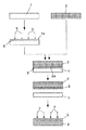
図1は、本発明による半導体基板の製造方法のフロー図である。
図1に示すように、本発明の半導体基板の製造方法は、半導体ウエハ1と透明な絶縁基板2を用いて、絶縁基板2上に半導体ウエハの半導体薄膜層3を有する半導体基板4を製造する方法である。
この例において、半導体ウエハ1はSiウエハであり、透明な絶縁基板2はガラス基板である。また以下、半導体ウエハの半導体薄膜層3をSOI薄膜層、半導体基板4をSOI薄膜層ウエハと呼ぶ。
図1に示すように、本発明の半導体基板の製造方法は、薄膜形成工程S1、貼合わせ工程S2、熱処理工程S3、剥離工程S4、及びレーザ光照射工程S5を備えている。
Hereinafter, embodiments of the present invention will be described with reference to the drawings.
FIG. 1 is a flowchart of a method for manufacturing a semiconductor substrate according to the present invention.
As shown in FIG. 1, the semiconductor substrate manufacturing method of the present invention uses a
In this example, the
As shown in FIG. 1, the manufacturing method of the semiconductor substrate of this invention is equipped with thin film formation process S1, bonding process S2, heat treatment process S3, peeling process S4, and laser beam irradiation process S5.
薄膜形成工程S1では、半導体ウエハ1にイオンを注入して半導体薄膜層を形成する。すなわち、この例において、Siウエハ1に表面1aから水素イオン5(或いは水素分子イオン、希ガスイオンまたはこれらの複合イオン)を注入することにより、Siウエハ1の内部に表面1aに対して平行な微小気泡層6を形成する。ここで、イオン注入の加速電圧を制御することにより、Siウエハ表面1aから所定の深さ位置に微小気泡層6(剥離層)を形成することができる。
In the thin film forming step S1, ions are implanted into the
貼合わせ工程S2では、薄膜形成工程S1の後に、半導体ウエハ1と絶縁基板2の表面を洗浄し、基板の一面を貼り合わせる。すなわち、上述した薄膜形成工程が終了した後に、Siウエハ1とガラス基板2を洗浄する。洗浄後、Siウエハの表面1aとガラス基板2の一面2aを貼り合わせる。
In the bonding step S2, after the thin film forming step S1, the surfaces of the
熱処理工程S3では、貼合わせ工程S2の後に、熱処理により貼合わせ面の接合強度を高める。すなわち、この例において、貼合わせ工程S2が終了した後に、300℃以上、400℃以下(例えば300℃、1時間)の温度条件で貼り合わせ処理したSiウエハ1とガラス基板2に熱処理を行う。Siウエハ1とガラス基板2の熱膨張係数は、同等がそれに近い特性であるため、熱膨張差によりSiウエハ1が割れることはない。例えば、293Kにおいて石英の熱膨張係数が約0.5×10⁻⁶に対し、シリコンは約3.65×10⁻⁶、パイレックス(登録商標)ガラスは約2.8×10⁻⁶である。
In the heat treatment step S3, the bonding strength of the bonding surface is increased by heat treatment after the bonding step S2. That is, in this example, after the bonding step S <b> 2 is completed, the
剥離工程S4では、熱処理工程S3の後に、半導体薄膜層を絶縁基板上に剥離させる。すなわち、この例において、低温熱処理工程S3が終了した後に、400℃以上、600℃以下(例えば、550℃、1時間)の条件で貼り合わせ処理したSiウエハ1とガラス基板2に熱処理を行う。これによって、微小気泡層6をへき開面としてSiウエハ1を薄膜状に剥離する。
In the peeling step S4, the semiconductor thin film layer is peeled off on the insulating substrate after the heat treatment step S3. That is, in this example, after the low-temperature heat treatment step S3 is completed, the heat treatment is performed on the
なお、上述した薄膜形成工程の代わりに、半導体ウエハの表面に多孔質構造を形成し、その上に半導体ウエハと同種のエピタキシャル層を成長させ、さらに、エピタキシャル層の表面に親水性の酸化膜を形成する工程としてもよい。
またこの場合、剥離工程を、ウォータージェットを半導体ウエハの表面の多孔質構造に吹き付けて、半導体薄膜を得るのがよい。
Instead of the thin film formation process described above, a porous structure is formed on the surface of the semiconductor wafer, an epitaxial layer of the same type as that of the semiconductor wafer is grown thereon, and a hydrophilic oxide film is formed on the surface of the epitaxial layer. It is good also as a process of forming.
In this case, it is preferable to obtain a semiconductor thin film by spraying a water jet onto the porous structure on the surface of the semiconductor wafer in the peeling step.
レーザ光照射工程S5では、剥離工程S4の後に、絶縁基板に、レーザ光を半導体薄膜層側または透明な絶縁基板側から照射して前記半導体薄膜層の結晶品質を改善するとともに、前記半導体薄膜層と前記透明な絶縁基板を強固に結合させる。
すなわち、この例において、剥離工程S4が終了した後に、レーザ照射装置(図示省略)によってレーザ光(例えば、YAGレーザの2倍波)7をSOI薄膜層3側またはガラス基板2側から照射する。これによって、SOI薄膜層3とガラス基板を強固に結合する。なお、レーザ光7はSOI薄膜層全面に照射するように行う。
In the laser beam irradiation step S5, after the peeling step S4, the insulating substrate is irradiated with laser light from the semiconductor thin film layer side or the transparent insulating substrate side to improve the crystal quality of the semiconductor thin film layer, and the semiconductor thin film layer And the transparent insulating substrate are firmly bonded.
That is, in this example, after the peeling step S4 is completed, a laser beam (for example, a double wave of YAG laser) 7 is irradiated from the SOI
ここで、レーザ光7を外側からガラス基板2に向かって照射することによって、SOI薄膜層3およびガラス基板2の界面のみを局部的に加熱でき、また、SOI薄膜層3とガラス基板2を強固に結合するまでの加熱時間(レーザ光7の照射時間)を極めて短くできる。例えば、本発明の実施形態では、加熱時間は数百ナノ秒である。一方、レーザ光7を外側から透明なガラス基板2に向かって照射しても、大部分のレーザ光7はガラス基板2を透過して、ガラス基板2の直接加熱に寄与するものではない。
Here, by irradiating the laser beam 7 from the outside toward the
以下にシリコン単結晶薄膜の実施例を説明する。
(1)試料準備
Siウエハは4インチ径、厚さ525μm、p型、面方位(100)、抵抗値0.5〜40Ωで100nm厚の熱酸化膜付きのものを用いた。ガラスウエハは、HOYA製NA35の無アルカリガラスを用い、4インチ径、厚さ0.7mmにものを作製し、500nmのSiO2膜をスパッタ成膜した。
(2)薄膜形成処理
酸化膜付Siウエハに水素イオン(H+)を加速電圧100kV、注入量5E16cm-2、入射角度0°(ウエハ表面に対して直交方向)で注入した。
(3)貼り合わせ処理
Siウエハおよびガラスウエハに対してSCIおよびSC2レベルのRCA洗浄を実施し、洗浄後、大気中、室温で貼り合わせた。
(4)Si薄膜の剥離処理および剥離後熱処理
Si薄膜の剥離は、Siウエハ同士を貼り合わせた試料に対して550℃、1時間の熱処理で、Siウエハとガラスウエハを貼り合わせた試料に対しては500℃、1時間の熱処理で行った。
Si薄膜の剥離後、窒素雰囲気で550℃、4時間の熱処理を実施し、レーザ照射用試料とした。
(5)レーザ照射工程
YLFレーザ(最大出力20W、波長527nm、繰り返し周波数1kHz)を光源として用い、試料をステージに載せ、搬送しながら照射した。
照射条件は、レーザ出力:4〜15W、ステージ搬送速度:3mm/秒、試料温度:室温で実施した。
Examples of the silicon single crystal thin film will be described below.
(1) Sample preparation A Si wafer having a diameter of 4 inches, a thickness of 525 μm, a p-type, a plane orientation (100), a resistance value of 0.5 to 40Ω and a thermal oxide film having a thickness of 100 nm was used. The glass wafer was made of HOYA NA35 non-alkali glass having a diameter of 4 inches and a thickness of 0.7 mm, and a 500 nm SiO 2 film was formed by sputtering.
(2) Thin film formation treatment Hydrogen ions (H + ) were implanted into an Si wafer with an oxide film at an acceleration voltage of 100 kV, an implantation amount of 5E16 cm −2 , and an incident angle of 0 ° (perpendicular to the wafer surface).
(3) Bonding treatment SCI and SC2 level RCA cleaning was performed on the Si wafer and the glass wafer, and after cleaning, they were bonded together in the atmosphere at room temperature.
(4) Si thin film peeling treatment and post-peeling heat treatment The Si thin film peeling is performed on a sample obtained by bonding a Si wafer and a glass wafer by heat treatment at 550 ° C. for 1 hour on a sample obtained by bonding Si wafers together. The heat treatment was performed at 500 ° C. for 1 hour.
After peeling off the Si thin film, heat treatment was performed at 550 ° C. for 4 hours in a nitrogen atmosphere to obtain a sample for laser irradiation.
(5) Laser irradiation process Using a YLF laser (maximum output 20 W, wavelength 527 nm,
Irradiation conditions were laser output: 4 to 15 W, stage conveyance speed: 3 mm / second, and sample temperature: room temperature.
図2は、レーザ出力とラマンの半値幅との関係図である。比較のため、市販のSOIウエハと比較した。その結果、レーザ出力10W以上で処理されたガラス基板上の薄膜が4.16cm-1を示し、市販のSOIウエハ3.95cm-1に近いレベルまで結晶品質を高めることができた。なお、現在、ガラス基板上に形成できる多結晶シリコンのラマンの半値幅は、5.1〜6 cm-1程度である。 FIG. 2 is a graph showing the relationship between the laser output and the half width of Raman. For comparison, it was compared with a commercially available SOI wafer. As a result, a thin film on a glass substrate which has been treated with laser output 10W or higher indicates 4.16Cm -1, it was possible to improve the crystal quality to a level close to the commercial SOI wafer 3.95cm -1. Currently, the half-value width of Raman of polycrystalline silicon that can be formed on a glass substrate is about 5.1 to 6 cm −1 .
図3は、レーザ出力と薄膜表面の最高到達温度との関係図であり、熱解析により求めたものである。その結果、薄膜のラマンの半値幅が4.16cm-1になるレーザ出力では、シリコンの融点以上であり、シリコンがレーザにより溶融、再結晶化していることが判明した。
本試験のように、パルスレーザを用い、半導体ウエハの融点を超える温度で加熱し、半導体薄膜を結晶化させることにより、半導体ウエハを溶融し、再結晶化することで、結晶品質を高めることができる。
FIG. 3 is a relationship diagram between the laser output and the maximum temperature reached on the surface of the thin film, and is obtained by thermal analysis. As a result, it was found that the laser output at which the half-value width of Raman of the thin film was 4.16 cm −1 was equal to or higher than the melting point of silicon, and that silicon was melted and recrystallized by the laser.
As in this test, by using a pulse laser and heating at a temperature exceeding the melting point of the semiconductor wafer to crystallize the semiconductor thin film, the semiconductor wafer is melted and recrystallized, thereby improving the crystal quality. it can.
図4は、剥離工程S4により、無アルカリガラス基板上へ剥離させたSi薄膜のラマン分光の測定結果を示す。この図において、横軸は波数、縦軸はラマン強度(相対強度)である。また、図中の実線は本発明の方法による半導体基板、破線は比較のための、単結晶シリコンウエハの結果である。
この図から、本発明の方法による半導体基板(無アルカリガラス基板上のSi薄膜)のラマン半値幅は、4.9cm−1、単結晶シリコンウエハのラマン半値幅は、4.6cm−1であり、無アルカリガラス基板上のSi薄膜の結晶品質がほぼ単結晶シリコンウエハの品質を保持していることがわかった。
FIG. 4 shows the measurement result of Raman spectroscopy of the Si thin film peeled off on the alkali-free glass substrate by the peeling step S4. In this figure, the horizontal axis represents the wave number, and the vertical axis represents the Raman intensity (relative intensity). Also, the solid line in the figure is the result of the semiconductor substrate by the method of the present invention, and the broken line is the result of the single crystal silicon wafer for comparison.
From this figure, the Raman half width of the semiconductor substrate (Si thin film on the alkali-free glass substrate) by the method of the present invention is 4.9 cm −1 , and the Raman half width of the single crystal silicon wafer is 4.6 cm −1 . It was found that the crystal quality of the Si thin film on the alkali-free glass substrate almost maintained the quality of the single crystal silicon wafer.
図5は、レーザ光の波長とガラスにおけるレーザ光の透過率との関係を示す図であり、図6は、レーザ光の波長とシリコンにおけるレーザ光の吸収係数との関係を示す図である。
レーザ光7がガラス基板2を十分に透過し、かつレーザ光7の光エネルギーがSiウエハ1に十分に吸収されるように、予めレーザ光7の波長を選択することが望ましい。すなわち、図5に示すようにレーザ光7の波長が380nm以上で2200nm以下の場合には、ガラスにおけるレーザ光7の透過率が90%になって、レーザ光7がガラス基板2を十分に透過することが判明している。
また、Siのバンドギャップを光の波長に変換すると、1100nm程度であることもあって、図6に示すようにレーザ光7の波長が780nm以下の場合であっても、レーザ光7の光SiウエハがSiウエハ1に十分吸収される。従って、380nm以上で2200nm以下のレーザ光7の波長を予め選択することよって、レーザ光7がガラス基板2を十分に透過しかつレーザ光7の光SiウエハがSiウエハ1に十分に吸収されることを確保できる。
FIG. 5 is a diagram showing the relationship between the wavelength of the laser beam and the transmittance of the laser beam in the glass, and FIG. 6 is a diagram showing the relationship between the wavelength of the laser beam and the absorption coefficient of the laser beam in silicon.
It is desirable to select the wavelength of the laser beam 7 in advance so that the laser beam 7 is sufficiently transmitted through the
Further, when the band gap of Si is converted to the wavelength of light, it may be about 1100 nm, and even if the wavelength of the laser beam 7 is 780 nm or less as shown in FIG. The wafer is sufficiently absorbed by the
また、前記絶縁基板と半導体ウエハの熱膨張係数は同等かそれに近い特性のものであることが望ましい。また、レーザ光7の発振は、パルスまたは連続発振のいずれでも差し支えない。また、レーザ光は、SOI薄膜側からでもガラス基板側からでも照射しても差し支えない。
なお、レーザ照射工程が終了した後に、薄膜層3の表面3aを鏡面研磨することが望ましい。
Further, it is desirable that the thermal expansion coefficients of the insulating substrate and the semiconductor wafer have the same or similar characteristics. Further, the laser beam 7 may be oscillated by either pulse or continuous oscillation. Further, the laser beam may be irradiated from the SOI thin film side or the glass substrate side.
In addition, it is desirable that the surface 3a of the
図7は、InPの温度と蒸気圧力の関係図である。この図において、横軸は1000/T(Tは温度K)、縦軸は蒸気圧力(atm)であり、図中の2本の曲線は、異なる分子構造を示している。
InPの融点は1333Kであり、この図の横軸0.75に相当し、蒸気圧力は、おおよそ2〜10atmとなる。
このような場合、本発明では、半導体ウエハの融点での蒸気圧が大気圧を超え、前記レーザ光を照射して溶融させて結晶化させる場合において、前記蒸気圧を超える圧力の不活性ガス雰囲気にて行うことにより、半導体薄膜層の分解を抑制しかつ半導体薄膜層の結晶品質を改善するとともに、半導体薄膜層と前記透明な絶縁基板を強固に結合させることができる。
FIG. 7 is a relationship diagram of InP temperature and vapor pressure. In this figure, the horizontal axis is 1000 / T (T is temperature K), the vertical axis is vapor pressure (atm), and the two curves in the figure indicate different molecular structures.
The melting point of InP is 1333K, which corresponds to the horizontal axis of 0.75 in this figure, and the vapor pressure is approximately 2 to 10 atm.
In such a case, in the present invention, the vapor pressure at the melting point of the semiconductor wafer exceeds atmospheric pressure, and when the laser beam is irradiated to melt and crystallize, an inert gas atmosphere having a pressure exceeding the vapor pressure is used. By performing the above, it is possible to suppress the decomposition of the semiconductor thin film layer and improve the crystal quality of the semiconductor thin film layer, and to firmly bond the semiconductor thin film layer and the transparent insulating substrate.
図8は、単結晶シリコンの温度と吸収係数の関係図である。この図において、常温(300K)に対して600Kにおける吸収係数は約2倍となる。
本発明では、前記レーザ照射工程は、前記半導体薄膜層が転写された絶縁基板を600℃以下の温度に加熱することで、半導体薄膜層の吸収係数が上昇するため、レーザ光の出力を下げることができる。
FIG. 8 is a graph showing the relationship between the temperature of single crystal silicon and the absorption coefficient. In this figure, the absorption coefficient at 600K is about twice that at room temperature (300K).
In the present invention, in the laser irradiation step, the insulating substrate onto which the semiconductor thin film layer is transferred is heated to a temperature of 600 ° C. or lower, so that the absorption coefficient of the semiconductor thin film layer is increased. Can do.
以上のごとき、本発明の実施の形態によれば、レーザ光7は、SOI薄膜層3に吸収する以外は、透明なガラス基板2を透過するため、ガラス基板2の直接加熱に関与するものではなく、また、SOI薄膜層3とガラス基板2を強固に結合するまでの加熱時間を極めて短くできるため、SOI薄膜層3を接合する基板は、例えば石英等の高い融点を有する高価なものに限られず、融点の低い安価なものも用いることができる。そのため、さまざまな構成材料からなるガラス基板2をSOI薄膜層ウエハ4の製造コストの低下を図ることができる。
As described above, according to the embodiment of the present invention, since the laser beam 7 is transmitted through the
また、本発明は、前述の発明の実施形態の説明に限るものではなく、例えば、半導体ウエハとして、Siウエハ、GaNウエハ、GaAsウエハ、SiCウエハ、InPウエハ、GaPなどの半導体ウエハのいずれかを用いたり、透明なガラス基板2の代わりに透明なプラスチック基板を用いる等、適宜の変更を行うことにより、その他さまざまな形態で実施可能である。
Further, the present invention is not limited to the description of the above-described embodiments of the invention. For example, any one of semiconductor wafers such as Si wafer, GaN wafer, GaAs wafer, SiC wafer, InP wafer, and GaP is used as the semiconductor wafer. It can be implemented in various other forms by making appropriate changes such as using a transparent plastic substrate instead of the
なお、本発明は上述した実施例及び実施形態に限定されず、本発明の要旨を逸脱しない範囲で種々変更できることは勿論である。 In addition, this invention is not limited to the Example and embodiment mentioned above, Of course, it can change variously in the range which does not deviate from the summary of this invention.
1 半導体ウエハ(Siウエハ)、1a 表面、
2 透明な絶縁基板(ガラス基板)、2a 一面、
3 半導体薄膜層(SOI薄膜層)、4 半導体基板(SOI薄膜層ウエハ)、
5 水素イオン(或いは水素分子イオン、希ガスイオンまたはこれらの複合イオン)、
6 微小気泡層(剥離層)、7 レーザ光(YAGレーザの2倍波)
1 semiconductor wafer (Si wafer), 1a surface,
2 Transparent insulating substrate (glass substrate), 2a,
3 Semiconductor thin film layer (SOI thin film layer), 4 Semiconductor substrate (SOI thin film layer wafer),
5 Hydrogen ions (or hydrogen molecular ions, rare gas ions or complex ions thereof),
6 Microbubble layer (peeling layer), 7 Laser light (twice wave of YAG laser)
Claims (11)
前記半導体ウエハとガラス基板とを、前記熱酸化膜と前記ガラス基板とが接するように貼り合わせる第2の工程と、
前記第2の工程後、熱処理を行う第3の工程と、
前記第3の工程後、前記半導体ウエハを前記微小気泡層において剥離して、前記ガラス基板上に半導体薄膜層を形成する第4の工程と、
前記第4の工程後、前記ガラス基板上の前記半導体薄膜層に対してレーザ光を照射する第5の工程とを備え、
前記第5の工程において、前記ガラス基板上の前記半導体薄膜層に対して前記レーザ光を照射する際に、前記ガラス基板を600℃以下の温度に加熱しながら行うことを特徴とする半導体薄膜層を有する基板の製造方法。 A first step of forming a microbubble layer inside a semiconductor wafer having a thermal oxide film formed on the surface;
A second step of bonding the semiconductor wafer and the glass substrate so that the thermal oxide film and the glass substrate are in contact with each other;
A third step of performing a heat treatment after the second step;
After the third step, a fourth step of peeling the semiconductor wafer in the microbubble layer to form a semiconductor thin film layer on the glass substrate;
After the fourth step, a fifth step of irradiating the semiconductor thin film layer on the glass substrate with a laser beam ,
In the fifth step, when irradiating the semiconductor thin film layer on the glass substrate with the laser light, the semiconductor thin film layer is performed while heating the glass substrate to a temperature of 600 ° C. or lower. The manufacturing method of the board | substrate which has this.
前記半導体ウエハとガラス基板とを、前記熱酸化膜と前記ガラス基板とが接するように貼り合わせる第2の工程と、
前記第2の工程後、熱処理を行う第3の工程と、
前記第3の工程後、前記半導体ウエハを前記剥離層において剥離して、前記ガラス基板上に半導体薄膜層を形成する第4の工程と、
前記第4の工程後、前記ガラス基板上の前記半導体薄膜層に対してレーザ光を照射する第5の工程とを備え、
前記第5の工程において、前記ガラス基板上の前記半導体薄膜層に対して前記レーザ光を照射する際に、前記ガラス基板を600℃以下の温度に加熱しながら行うことを特徴とする半導体薄膜層を有する基板の製造方法。 A first step of forming a release layer inside a semiconductor wafer having a thermal oxide film formed on the surface;
A second step of bonding the semiconductor wafer and the glass substrate so that the thermal oxide film and the glass substrate are in contact with each other;
A third step of performing a heat treatment after the second step;
After the third step, a fourth step of peeling the semiconductor wafer at the release layer to form a semiconductor thin film layer on the glass substrate;
After the fourth step, a fifth step of irradiating the semiconductor thin film layer on the glass substrate with a laser beam ,
In the fifth step, when irradiating the semiconductor thin film layer on the glass substrate with the laser light, the semiconductor thin film layer is performed while heating the glass substrate to a temperature of 600 ° C. or lower. The manufacturing method of the board | substrate which has this.
Priority Applications (1)
| Application Number | Priority Date | Filing Date | Title |
|---|---|---|---|
| JP2005024838A JP5110772B2 (en) | 2004-02-03 | 2005-02-01 | Manufacturing method of substrate having semiconductor thin film layer |
Applications Claiming Priority (3)
| Application Number | Priority Date | Filing Date | Title |
|---|---|---|---|
| JP2004026584 | 2004-02-03 | ||
| JP2004026584 | 2004-02-03 | ||
| JP2005024838A JP5110772B2 (en) | 2004-02-03 | 2005-02-01 | Manufacturing method of substrate having semiconductor thin film layer |
Related Child Applications (1)
| Application Number | Title | Priority Date | Filing Date |
|---|---|---|---|
| JP2008286231A Division JP5358159B2 (en) | 2004-02-03 | 2008-11-07 | Manufacturing method of substrate having semiconductor thin film layer |
Publications (3)
| Publication Number | Publication Date |
|---|---|
| JP2005252244A JP2005252244A (en) | 2005-09-15 |
| JP2005252244A5 JP2005252244A5 (en) | 2008-12-25 |
| JP5110772B2 true JP5110772B2 (en) | 2012-12-26 |
Family
ID=35032391
Family Applications (1)
| Application Number | Title | Priority Date | Filing Date |
|---|---|---|---|
| JP2005024838A Expired - Fee Related JP5110772B2 (en) | 2004-02-03 | 2005-02-01 | Manufacturing method of substrate having semiconductor thin film layer |
Country Status (1)
| Country | Link |
|---|---|
| JP (1) | JP5110772B2 (en) |
Cited By (1)
| Publication number | Priority date | Publication date | Assignee | Title |
|---|---|---|---|---|
| CN109287126A (en) * | 2017-05-19 | 2019-01-29 | 日本新工芯技株式会社 | The manufacturing method and endless member of endless member |
Families Citing this family (82)
| Publication number | Priority date | Publication date | Assignee | Title |
|---|---|---|---|---|
| JP5103607B2 (en) * | 2005-11-04 | 2012-12-19 | 国立大学法人東京農工大学 | Release layer removal method |
| US7579654B2 (en) * | 2006-05-31 | 2009-08-25 | Corning Incorporated | Semiconductor on insulator structure made using radiation annealing |
| JP5003033B2 (en) | 2006-06-30 | 2012-08-15 | 住友電気工業株式会社 | GaN thin film bonded substrate and manufacturing method thereof, and GaN-based semiconductor device and manufacturing method thereof |
| JP5284576B2 (en) * | 2006-11-10 | 2013-09-11 | 信越化学工業株式会社 | Manufacturing method of semiconductor substrate |
| JP5019852B2 (en) * | 2006-11-10 | 2012-09-05 | 信越化学工業株式会社 | Method for manufacturing strained silicon substrate |
| WO2008123116A1 (en) | 2007-03-26 | 2008-10-16 | Semiconductor Energy Laboratory Co., Ltd. | Soi substrate and method for manufacturing soi substrate |
| WO2008123117A1 (en) | 2007-03-26 | 2008-10-16 | Semiconductor Energy Laboratory Co., Ltd. | Soi substrate and method for manufacturing soi substrate |
| CN101281912B (en) | 2007-04-03 | 2013-01-23 | 株式会社半导体能源研究所 | Soi substrate and manufacturing method thereof, and semiconductor device |
| SG178762A1 (en) | 2007-04-13 | 2012-03-29 | Semiconductor Energy Lab | Display device, method for manufacturing display device, and soi substrate |
| KR101440930B1 (en) | 2007-04-20 | 2014-09-15 | 가부시키가이샤 한도오따이 에네루기 켄큐쇼 | Method of manufacturing soi substrate |
| US7767542B2 (en) * | 2007-04-20 | 2010-08-03 | Semiconductor Energy Laboratory Co., Ltd | Manufacturing method of SOI substrate |
| US7635617B2 (en) * | 2007-04-27 | 2009-12-22 | Semiconductor Energy Laboratory Co., Ltd. | Manufacturing method of semiconductor substrate and manufacturing method of semiconductor device |
| JP5289805B2 (en) | 2007-05-10 | 2013-09-11 | 株式会社半導体エネルギー研究所 | Method for manufacturing substrate for manufacturing semiconductor device |
| KR101443580B1 (en) | 2007-05-11 | 2014-10-30 | 가부시키가이샤 한도오따이 에네루기 켄큐쇼 | Method for manufacturing semiconductor device |
| US7825007B2 (en) | 2007-05-11 | 2010-11-02 | Semiconductor Energy Laboratory Co., Ltd. | Method of joining a plurality of SOI substrates on a glass substrate by a heat treatment |
| US8513678B2 (en) | 2007-05-18 | 2013-08-20 | Semiconductor Energy Laboratory Co., Ltd. | Light-emitting device |
| US7960262B2 (en) | 2007-05-18 | 2011-06-14 | Semiconductor Energy Laboratory Co., Ltd. | Method for manufacturing semiconductor device by applying laser beam to single-crystal semiconductor layer and non-single-crystal semiconductor layer through cap film |
| EP1993127B1 (en) | 2007-05-18 | 2013-04-24 | Semiconductor Energy Laboratory Co., Ltd. | Manufacturing method of SOI substrate |
| US7745268B2 (en) * | 2007-06-01 | 2010-06-29 | Semiconductor Energy Laboratory Co., Ltd. | Method for manufacturing a semiconductor device with irradiation of single crystal semiconductor layer in an inert atmosphere |
| DE202007019495U1 (en) | 2007-06-06 | 2013-01-10 | Sumitomo Electric Industries, Ltd. | Substrate with GaN thin film and GaN-based semiconductor device coated thereon |
| CN101681843B (en) | 2007-06-20 | 2012-05-09 | 株式会社半导体能源研究所 | Method of manufacturing semiconductor device |
| KR101484296B1 (en) * | 2007-06-26 | 2015-01-19 | 가부시키가이샤 한도오따이 에네루기 켄큐쇼 | Semiconductor substrate, manufacturing method of the semiconductor substrate, and semiconductor device and electronic device using the same |
| US7795111B2 (en) | 2007-06-27 | 2010-09-14 | Semiconductor Energy Laboratory Co., Ltd. | Manufacturing method of SOI substrate and manufacturing method of semiconductor device |
| WO2009001836A1 (en) | 2007-06-28 | 2008-12-31 | Semiconductor Energy Laboratory Co., Ltd. | Manufacturing method of semiconductor device |
| US8431451B2 (en) | 2007-06-29 | 2013-04-30 | Semicondutor Energy Laboratory Co., Ltd. | Display device and method for manufacturing the same |
| EP2009687B1 (en) * | 2007-06-29 | 2016-08-17 | Semiconductor Energy Laboratory Co., Ltd. | Method of manufacturing an SOI substrate and method of manufacturing a semiconductor device |
| US7678668B2 (en) | 2007-07-04 | 2010-03-16 | Semiconductor Energy Laboratory Co., Ltd. | Manufacturing method of SOI substrate and manufacturing method of semiconductor device |
| JP5463017B2 (en) * | 2007-09-21 | 2014-04-09 | 株式会社半導体エネルギー研究所 | Substrate manufacturing method |
| JP2009094488A (en) * | 2007-09-21 | 2009-04-30 | Semiconductor Energy Lab Co Ltd | Method of manufacturing substrate provided with semiconductor film |
| KR101499175B1 (en) | 2007-10-04 | 2015-03-05 | 가부시키가이샤 한도오따이 에네루기 켄큐쇼 | Method for manufacturing semiconductor substrate |
| US8236668B2 (en) | 2007-10-10 | 2012-08-07 | Semiconductor Energy Laboratory Co., Ltd. | Method for manufacturing SOI substrate |
| JP2009135430A (en) * | 2007-10-10 | 2009-06-18 | Semiconductor Energy Lab Co Ltd | Method of manufacturing semiconductor device |
| US7799658B2 (en) | 2007-10-10 | 2010-09-21 | Semiconductor Energy Laboratory Co., Ltd. | Method for manufacturing semiconductor substrate and method for manufacturing semiconductor device |
| JP5490393B2 (en) | 2007-10-10 | 2014-05-14 | 株式会社半導体エネルギー研究所 | Manufacturing method of semiconductor substrate |
| JP5527956B2 (en) * | 2007-10-10 | 2014-06-25 | 株式会社半導体エネルギー研究所 | Manufacturing method of semiconductor substrate |
| JP5522917B2 (en) | 2007-10-10 | 2014-06-18 | 株式会社半導体エネルギー研究所 | Manufacturing method of SOI substrate |
| JP2009135453A (en) | 2007-10-30 | 2009-06-18 | Semiconductor Energy Lab Co Ltd | Method for manufacturing semiconductor device, semiconductor device, and electronic device |
| US7851318B2 (en) * | 2007-11-01 | 2010-12-14 | Semiconductor Energy Laboratory Co., Ltd. | Semiconductor substrate and method for manufacturing the same, and method for manufacturing semiconductor device |
| WO2009057669A1 (en) | 2007-11-01 | 2009-05-07 | Semiconductor Energy Laboratory Co., Ltd. | Method for manufacturing photoelectric conversion device |
| JP2009135448A (en) * | 2007-11-01 | 2009-06-18 | Semiconductor Energy Lab Co Ltd | Method for manufacturing semiconductor substrate, and method for manufacturing semiconductor device |
| US8163628B2 (en) * | 2007-11-01 | 2012-04-24 | Semiconductor Energy Laboratory Co., Ltd. | Method for manufacturing semiconductor substrate |
| US7816234B2 (en) | 2007-11-05 | 2010-10-19 | Semiconductor Energy Laboratory Co., Ltd. | Method for manufacturing semiconductor device |
| JP2009151293A (en) | 2007-11-30 | 2009-07-09 | Semiconductor Energy Lab Co Ltd | Display device, manufacturing method of display device and electronic equipment |
| US7842583B2 (en) * | 2007-12-27 | 2010-11-30 | Semiconductor Energy Laboratory Co., Ltd. | Method for manufacturing semiconductor substrate and method for manufacturing semiconductor device |
| US7947570B2 (en) | 2008-01-16 | 2011-05-24 | Semiconductor Energy Laboratory Co., Ltd. | Manufacturing method and manufacturing apparatus of semiconductor substrate |
| JP5404064B2 (en) | 2008-01-16 | 2014-01-29 | 株式会社半導体エネルギー研究所 | Laser processing apparatus and semiconductor substrate manufacturing method |
| JP5503876B2 (en) | 2008-01-24 | 2014-05-28 | 株式会社半導体エネルギー研究所 | Manufacturing method of semiconductor substrate |
| US8003483B2 (en) * | 2008-03-18 | 2011-08-23 | Semiconductor Energy Laboratory Co., Ltd. | Method for manufacturing SOI substrate |
| JP5411438B2 (en) * | 2008-03-18 | 2014-02-12 | 信越化学工業株式会社 | Manufacturing method of SOI substrate |
| JP2009260315A (en) | 2008-03-26 | 2009-11-05 | Semiconductor Energy Lab Co Ltd | Method for manufacturing soi substrate, and method for manufacturing semiconductor device |
| JP5654206B2 (en) | 2008-03-26 | 2015-01-14 | 株式会社半導体エネルギー研究所 | Method for manufacturing SOI substrate and semiconductor device using the SOI substrate |
| JP2009260313A (en) | 2008-03-26 | 2009-11-05 | Semiconductor Energy Lab Co Ltd | Method for manufacturing soi substrate, and method for manufacturing semiconductor device |
| EP2105957A3 (en) | 2008-03-26 | 2011-01-19 | Semiconductor Energy Laboratory Co., Ltd. | Method for manufacturing soi substrate and method for manufacturing semiconductor device |
| US7939389B2 (en) | 2008-04-18 | 2011-05-10 | Semiconductor Energy Laboratory Co., Ltd. | Semiconductor device and method for manufacturing the same |
| JP5700617B2 (en) | 2008-07-08 | 2015-04-15 | 株式会社半導体エネルギー研究所 | Method for manufacturing SOI substrate |
| JP5552276B2 (en) | 2008-08-01 | 2014-07-16 | 株式会社半導体エネルギー研究所 | Method for manufacturing SOI substrate |
| JP5580010B2 (en) | 2008-09-05 | 2014-08-27 | 株式会社半導体エネルギー研究所 | Method for manufacturing semiconductor device |
| US20100081251A1 (en) * | 2008-09-29 | 2010-04-01 | Semiconductor Energy Laboratory Co., Ltd. | Method for manufacturing soi substrate |
| SG160302A1 (en) | 2008-09-29 | 2010-04-29 | Semiconductor Energy Lab | Method for manufacturing semiconductor substrate |
| SG160295A1 (en) * | 2008-09-29 | 2010-04-29 | Semiconductor Energy Lab | Method for manufacturing semiconductor device |
| US8741740B2 (en) | 2008-10-02 | 2014-06-03 | Semiconductor Energy Laboratory Co., Ltd. | Method for manufacturing SOI substrate |
| SG160310A1 (en) | 2008-10-02 | 2010-04-29 | Semiconductor Energy Lab | Manufacturing method of semiconductor substrate and semiconductor device |
| JP2010114431A (en) | 2008-10-10 | 2010-05-20 | Semiconductor Energy Lab Co Ltd | Method of manufacturing soi substrate |
| SG161151A1 (en) | 2008-10-22 | 2010-05-27 | Semiconductor Energy Lab | Soi substrate and method for manufacturing the same |
| JP5389627B2 (en) * | 2008-12-11 | 2014-01-15 | 信越化学工業株式会社 | Manufacturing method of composite substrate with wide band gap semiconductor laminated |
| SG182208A1 (en) | 2008-12-15 | 2012-07-30 | Semiconductor Energy Lab | Manufacturing method of soi substrate and manufacturing method of semiconductor device |
| SG163481A1 (en) * | 2009-01-21 | 2010-08-30 | Semiconductor Energy Lab | Method for manufacturing soi substrate and semiconductor device |
| SG166060A1 (en) | 2009-04-22 | 2010-11-29 | Semiconductor Energy Lab | Method of manufacturing soi substrate |
| US8043938B2 (en) * | 2009-05-14 | 2011-10-25 | Semiconductor Energy Laboratory Co., Ltd. | Method for manufacturing SOI substrate and SOI substrate |
| JP2011029609A (en) | 2009-06-26 | 2011-02-10 | Semiconductor Energy Lab Co Ltd | Method for manufacturing soi substrate, and soi substrate |
| JP5713603B2 (en) | 2009-09-02 | 2015-05-07 | 株式会社半導体エネルギー研究所 | Method for manufacturing SOI substrate |
| JP2011077504A (en) | 2009-09-02 | 2011-04-14 | Semiconductor Energy Lab Co Ltd | Method for manufacturing semiconductor device |
| JP5846727B2 (en) * | 2009-09-04 | 2016-01-20 | 株式会社半導体エネルギー研究所 | Method for manufacturing semiconductor substrate |
| JP5587107B2 (en) * | 2009-09-18 | 2014-09-10 | 株式会社半導体エネルギー研究所 | Method for manufacturing SOI substrate |
| JP5866088B2 (en) | 2009-11-24 | 2016-02-17 | 株式会社半導体エネルギー研究所 | Method for manufacturing SOI substrate |
| JP5926887B2 (en) | 2010-02-03 | 2016-05-25 | 株式会社半導体エネルギー研究所 | Method for manufacturing SOI substrate |
| FR2961719B1 (en) * | 2010-06-24 | 2013-09-27 | Soitec Silicon On Insulator | PROCESS FOR PROCESSING A PIECE OF A COMPOUND MATERIAL |
| JP5688709B2 (en) * | 2010-09-24 | 2015-03-25 | 国立大学法人東京農工大学 | Method for manufacturing thin film semiconductor substrate |
| TWI500118B (en) | 2010-11-12 | 2015-09-11 | Semiconductor Energy Lab | Method for manufacturing semiconductor substrate |
| US8802534B2 (en) | 2011-06-14 | 2014-08-12 | Semiconductor Energy Laboratory Co., Ltd. | Method for forming SOI substrate and apparatus for forming the same |
| US9029238B2 (en) * | 2012-10-11 | 2015-05-12 | International Business Machines Corporation | Advanced handler wafer bonding and debonding |
| CN108598218B (en) * | 2018-04-26 | 2020-08-11 | 上海空间电源研究所 | Epitaxial layer rigid-flexible substrate inorganic bonding transfer method |
Family Cites Families (9)
| Publication number | Priority date | Publication date | Assignee | Title |
|---|---|---|---|---|
| JPH08203659A (en) * | 1995-01-26 | 1996-08-09 | Hitachi Ltd | Heating device |
| JPH1197379A (en) * | 1997-07-25 | 1999-04-09 | Denso Corp | Semiconductor substrate and its manufacture |
| JPH11145438A (en) * | 1997-11-13 | 1999-05-28 | Shin Etsu Handotai Co Ltd | Method of manufacturing soi wafer and soi wafer manufactured by the method |
| JPH11163363A (en) * | 1997-11-22 | 1999-06-18 | Semiconductor Energy Lab Co Ltd | Semiconductor device and its forming method |
| US5909627A (en) * | 1998-05-18 | 1999-06-01 | Philips Electronics North America Corporation | Process for production of thin layers of semiconductor material |
| JP2000150835A (en) * | 1998-11-05 | 2000-05-30 | Fujitsu Ltd | Manufacture of non-single crystal silicon thin-film |
| JP2001319891A (en) * | 2000-05-10 | 2001-11-16 | Nec Corp | Method and apparatus for processing thin film |
| JP2003282885A (en) * | 2002-03-26 | 2003-10-03 | Sharp Corp | Semiconductor device and its fabricating method |
| JP4759919B2 (en) * | 2004-01-16 | 2011-08-31 | セイコーエプソン株式会社 | Manufacturing method of electro-optical device |
-
2005
- 2005-02-01 JP JP2005024838A patent/JP5110772B2/en not_active Expired - Fee Related
Cited By (2)
| Publication number | Priority date | Publication date | Assignee | Title |
|---|---|---|---|---|
| CN109287126A (en) * | 2017-05-19 | 2019-01-29 | 日本新工芯技株式会社 | The manufacturing method and endless member of endless member |
| CN109287126B (en) * | 2017-05-19 | 2021-11-09 | 日本新工芯技株式会社 | Method for manufacturing annular member and annular member |
Also Published As
| Publication number | Publication date |
|---|---|
| JP2005252244A (en) | 2005-09-15 |
Similar Documents
| Publication | Publication Date | Title |
|---|---|---|
| JP5110772B2 (en) | Manufacturing method of substrate having semiconductor thin film layer | |
| CN101454875B (en) | Semiconductor on insulator structure made using radiation annealing | |
| JP5128761B2 (en) | Manufacturing method of SOI wafer | |
| KR100972213B1 (en) | Process for producing soi wafer and soi wafer | |
| KR100279756B1 (en) | Manufacturing method of semiconductor article | |
| JP2005252244A5 (en) | ||
| JP2007184581A (en) | Semiconductor on glass insulator prepared by using improved ion implatation process | |
| JPH05275663A (en) | Semiconductor element substrate and manufacture thereof | |
| JP6168143B2 (en) | Method for manufacturing hybrid substrate | |
| JPH1197379A (en) | Semiconductor substrate and its manufacture | |
| KR20130029110A (en) | Method for finishing silicon on insulator substrates | |
| JP2006210898A (en) | Process for producing soi wafer, and soi wafer | |
| JP2010538459A (en) | Reuse of semiconductor wafers in delamination processes using heat treatment | |
| WO2007074551A1 (en) | Process for producing soi wafer and soi wafer | |
| JP5496540B2 (en) | Method for manufacturing semiconductor substrate | |
| JP4624812B2 (en) | Manufacturing method of SOI wafer | |
| JP2010098167A (en) | Method of manufacturing laminated wafer | |
| JP5292810B2 (en) | Manufacturing method of SOI substrate | |
| JP3262470B2 (en) | Semiconductor substrate and manufacturing method thereof | |
| JP5358159B2 (en) | Manufacturing method of substrate having semiconductor thin film layer | |
| JP4594121B2 (en) | Manufacturing method of SOI wafer and SOI wafer | |
| KR20080085693A (en) | Soi wafer and manufacturing method thereof | |
| JP2961522B2 (en) | Substrate for semiconductor electronic device and method of manufacturing the same | |
| JPH11330438A (en) | Manufacture of soi wafer and soi wafer | |
| JP3293767B2 (en) | Semiconductor member manufacturing method |
Legal Events
| Date | Code | Title | Description |
|---|---|---|---|
| A621 | Written request for application examination |
Free format text: JAPANESE INTERMEDIATE CODE: A621 Effective date: 20071220 |
|
| A711 | Notification of change in applicant |
Free format text: JAPANESE INTERMEDIATE CODE: A711 Effective date: 20080905 |
|
| A521 | Written amendment |
Free format text: JAPANESE INTERMEDIATE CODE: A523 Effective date: 20081107 |
|
| A977 | Report on retrieval |
Free format text: JAPANESE INTERMEDIATE CODE: A971007 Effective date: 20110808 |
|
| A131 | Notification of reasons for refusal |
Free format text: JAPANESE INTERMEDIATE CODE: A131 Effective date: 20110816 |
|
| A521 | Written amendment |
Free format text: JAPANESE INTERMEDIATE CODE: A523 Effective date: 20111007 |
|
| A02 | Decision of refusal |
Free format text: JAPANESE INTERMEDIATE CODE: A02 Effective date: 20120327 |
|
| A521 | Written amendment |
Free format text: JAPANESE INTERMEDIATE CODE: A523 Effective date: 20120625 |
|
| A911 | Transfer of reconsideration by examiner before appeal (zenchi) |
Free format text: JAPANESE INTERMEDIATE CODE: A911 Effective date: 20120702 |
|
| TRDD | Decision of grant or rejection written | ||
| A01 | Written decision to grant a patent or to grant a registration (utility model) |
Free format text: JAPANESE INTERMEDIATE CODE: A01 Effective date: 20121002 |
|
| A01 | Written decision to grant a patent or to grant a registration (utility model) |
Free format text: JAPANESE INTERMEDIATE CODE: A01 |
|
| A61 | First payment of annual fees (during grant procedure) |
Free format text: JAPANESE INTERMEDIATE CODE: A61 Effective date: 20121009 |
|
| FPAY | Renewal fee payment (event date is renewal date of database) |
Free format text: PAYMENT UNTIL: 20151019 Year of fee payment: 3 |
|
| R150 | Certificate of patent or registration of utility model |
Free format text: JAPANESE INTERMEDIATE CODE: R150 |
|
| FPAY | Renewal fee payment (event date is renewal date of database) |
Free format text: PAYMENT UNTIL: 20151019 Year of fee payment: 3 |
|
| R250 | Receipt of annual fees |
Free format text: JAPANESE INTERMEDIATE CODE: R250 |
|
| R250 | Receipt of annual fees |
Free format text: JAPANESE INTERMEDIATE CODE: R250 |
|
| LAPS | Cancellation because of no payment of annual fees |