JP5244973B2 - Photodetector and fluid measuring device - Google Patents
Photodetector and fluid measuring device Download PDFInfo
- Publication number
- JP5244973B2 JP5244973B2 JP2011517693A JP2011517693A JP5244973B2 JP 5244973 B2 JP5244973 B2 JP 5244973B2 JP 2011517693 A JP2011517693 A JP 2011517693A JP 2011517693 A JP2011517693 A JP 2011517693A JP 5244973 B2 JP5244973 B2 JP 5244973B2
- Authority
- JP
- Japan
- Prior art keywords
- current
- light
- output
- photoelectric conversion
- conversion element
- Prior art date
- Legal status (The legal status is an assumption and is not a legal conclusion. Google has not performed a legal analysis and makes no representation as to the accuracy of the status listed.)
- Active
Links
- 239000012530 fluid Substances 0.000 title claims description 16
- 238000006243 chemical reaction Methods 0.000 claims abstract description 173
- 230000003287 optical effect Effects 0.000 claims abstract description 7
- 238000001514 detection method Methods 0.000 claims description 105
- 238000005259 measurement Methods 0.000 claims description 5
- 230000001678 irradiating effect Effects 0.000 claims 1
- 230000017531 blood circulation Effects 0.000 description 36
- 238000010586 diagram Methods 0.000 description 20
- 239000004065 semiconductor Substances 0.000 description 11
- 101100434411 Saccharomyces cerevisiae (strain ATCC 204508 / S288c) ADH1 gene Proteins 0.000 description 4
- 101150102866 adc1 gene Proteins 0.000 description 4
- 101150042711 adc2 gene Proteins 0.000 description 4
- 101100381996 Saccharomyces cerevisiae (strain ATCC 204508 / S288c) BRO1 gene Proteins 0.000 description 3
- 230000003321 amplification Effects 0.000 description 3
- 239000000470 constituent Substances 0.000 description 3
- 238000003199 nucleic acid amplification method Methods 0.000 description 3
- 238000010248 power generation Methods 0.000 description 3
- 229920006395 saturated elastomer Polymers 0.000 description 3
- 102000001554 Hemoglobins Human genes 0.000 description 1
- 108010054147 Hemoglobins Proteins 0.000 description 1
- 238000005513 bias potential Methods 0.000 description 1
- 230000005540 biological transmission Effects 0.000 description 1
- 239000003990 capacitor Substances 0.000 description 1
- 230000000694 effects Effects 0.000 description 1
- 238000010606 normalization Methods 0.000 description 1
- 238000005070 sampling Methods 0.000 description 1
- 238000001228 spectrum Methods 0.000 description 1
Images


Classifications
-
- A—HUMAN NECESSITIES
- A61—MEDICAL OR VETERINARY SCIENCE; HYGIENE
- A61B—DIAGNOSIS; SURGERY; IDENTIFICATION
- A61B5/00—Measuring for diagnostic purposes; Identification of persons
- A61B5/02—Detecting, measuring or recording pulse, heart rate, blood pressure or blood flow; Combined pulse/heart-rate/blood pressure determination; Evaluating a cardiovascular condition not otherwise provided for, e.g. using combinations of techniques provided for in this group with electrocardiography or electroauscultation; Heart catheters for measuring blood pressure
- A61B5/026—Measuring blood flow
- A61B5/0261—Measuring blood flow using optical means, e.g. infrared light
-
- G—PHYSICS
- G01—MEASURING; TESTING
- G01F—MEASURING VOLUME, VOLUME FLOW, MASS FLOW OR LIQUID LEVEL; METERING BY VOLUME
- G01F1/00—Measuring the volume flow or mass flow of fluid or fluent solid material wherein the fluid passes through a meter in a continuous flow
- G01F1/66—Measuring the volume flow or mass flow of fluid or fluent solid material wherein the fluid passes through a meter in a continuous flow by measuring frequency, phase shift or propagation time of electromagnetic or other waves, e.g. using ultrasonic flowmeters
- G01F1/661—Measuring the volume flow or mass flow of fluid or fluent solid material wherein the fluid passes through a meter in a continuous flow by measuring frequency, phase shift or propagation time of electromagnetic or other waves, e.g. using ultrasonic flowmeters using light
-
- G—PHYSICS
- G01—MEASURING; TESTING
- G01F—MEASURING VOLUME, VOLUME FLOW, MASS FLOW OR LIQUID LEVEL; METERING BY VOLUME
- G01F1/00—Measuring the volume flow or mass flow of fluid or fluent solid material wherein the fluid passes through a meter in a continuous flow
- G01F1/66—Measuring the volume flow or mass flow of fluid or fluent solid material wherein the fluid passes through a meter in a continuous flow by measuring frequency, phase shift or propagation time of electromagnetic or other waves, e.g. using ultrasonic flowmeters
- G01F1/663—Measuring the volume flow or mass flow of fluid or fluent solid material wherein the fluid passes through a meter in a continuous flow by measuring frequency, phase shift or propagation time of electromagnetic or other waves, e.g. using ultrasonic flowmeters by measuring Doppler frequency shift
-
- G—PHYSICS
- G01—MEASURING; TESTING
- G01F—MEASURING VOLUME, VOLUME FLOW, MASS FLOW OR LIQUID LEVEL; METERING BY VOLUME
- G01F1/00—Measuring the volume flow or mass flow of fluid or fluent solid material wherein the fluid passes through a meter in a continuous flow
- G01F1/66—Measuring the volume flow or mass flow of fluid or fluent solid material wherein the fluid passes through a meter in a continuous flow by measuring frequency, phase shift or propagation time of electromagnetic or other waves, e.g. using ultrasonic flowmeters
- G01F1/667—Arrangements of transducers for ultrasonic flowmeters; Circuits for operating ultrasonic flowmeters
-
- G—PHYSICS
- G01—MEASURING; TESTING
- G01P—MEASURING LINEAR OR ANGULAR SPEED, ACCELERATION, DECELERATION, OR SHOCK; INDICATING PRESENCE, ABSENCE, OR DIRECTION, OF MOVEMENT
- G01P5/00—Measuring speed of fluids, e.g. of air stream; Measuring speed of bodies relative to fluids, e.g. of ship, of aircraft
- G01P5/26—Measuring speed of fluids, e.g. of air stream; Measuring speed of bodies relative to fluids, e.g. of ship, of aircraft by measuring the direct influence of the streaming fluid on the properties of a detecting optical wave
-
- G—PHYSICS
- G01—MEASURING; TESTING
- G01S—RADIO DIRECTION-FINDING; RADIO NAVIGATION; DETERMINING DISTANCE OR VELOCITY BY USE OF RADIO WAVES; LOCATING OR PRESENCE-DETECTING BY USE OF THE REFLECTION OR RERADIATION OF RADIO WAVES; ANALOGOUS ARRANGEMENTS USING OTHER WAVES
- G01S17/00—Systems using the reflection or reradiation of electromagnetic waves other than radio waves, e.g. lidar systems
- G01S17/02—Systems using the reflection of electromagnetic waves other than radio waves
- G01S17/50—Systems of measurement based on relative movement of target
- G01S17/58—Velocity or trajectory determination systems; Sense-of-movement determination systems
Abstract
Description
本発明は、例えば被検体によって例えば反射、散乱等された光に含まれる信号光成分を検出するための光検出装置、及び該光検出装置を備えた、例えばレーザートップラー血流計等の流体計測装置の技術分野に関する。 The present invention relates to a light detection device for detecting a signal light component included in light reflected, scattered, etc., for example, by a subject, and a fluid, such as a laser topler blood flow meter, provided with the light detection device. The present invention relates to the technical field of measuring devices.
この種の光検出装置として、例えば、レーザートップラー血流計において生体からの光を検出する受光部として用いられるものがある(例えば特許文献1及び2参照)。レーザードップラー血流計は、レーザー光等の光を生体に照射し、その反射又は散乱の際におけるドップラーシフトによる波長の変化により、生体の血流速度等を算出する。このようなレーザートップラー血流計における受光部として用いられる光検出装置は、典型的には、フォトダイオード等の光電変換素子と、この光電変換素子の出力電流を増幅して電圧信号に変換する、オペアンプ(即ち「演算増幅回路」)を含む電流電圧変換回路とを備えている。
As this type of light detection device, for example, there is a device used as a light receiving unit for detecting light from a living body in a laser topler blood flow meter (see, for example,
一方、例えば特許文献3には、光通信等に使用される光受信回路において、フォトダイオードの両端にバイアス素子を接続すると共に、この両端をコンデンサを介して差動アンプ(オペアンプ)の入力端に接続し、且つ、差動アンプの正入力と反転出力との間および負入力と正出力との間に抵抗素子を設けることが開示されている。 On the other hand, for example, in Patent Document 3, in an optical receiving circuit used for optical communication or the like, a bias element is connected to both ends of a photodiode, and both ends are connected to an input terminal of a differential amplifier (op-amp) via a capacitor. It is disclosed that a resistance element is provided between the positive input and the inverted output of the differential amplifier and between the negative input and the positive output.
この種の光検出装置が前述したようなレーザードップラー血流計における受光部として用いられる場合、生体によって反射又は散乱された光に含まれる信号光成分(即ち、ドップラーシフトされた変調成分)の強度は、生体によって反射又は散乱された光に含まれる定常光成分(即ち、生体による反射又は散乱によって変動しない成分)の強度よりも微弱であるため、信号光成分を精度良く検出することが困難であるという技術的問題点がある。 When this type of light detection device is used as a light receiving unit in a laser Doppler blood flow meter as described above, the intensity of a signal light component (that is, a Doppler shifted modulation component) included in light reflected or scattered by a living body. Is weaker than the intensity of the steady light component contained in the light reflected or scattered by the living body (that is, the component that does not vary due to reflection or scattering by the living body), and it is difficult to detect the signal light component with high accuracy. There is a technical problem.
本発明は、例えば前述した問題点に鑑みなされたものであり、例えば被検体によって例えば反射、散乱等された光に含まれる信号光成分を精度良く検出することが可能な光検出装置、及びこのような光検出装置を備えた流体計測装置を提供することを課題とする。 The present invention has been made in view of, for example, the above-described problems. For example, a photodetection device capable of accurately detecting a signal light component included in light reflected or scattered by a subject, and the like, and this It is an object of the present invention to provide a fluid measuring device including such a light detection device.
本発明の光検出装置は上記課題を解決するために、入力光に含まれる信号光成分を検出するための光検出装置であって、前記入力光を電流に夫々変換して出力する第1及び第2光電変換素子部を含んでなり、前記第1光電変換素子部が出力する電流と前記第2光電変換素子部が出力する電流との差分電流を検出電流として出力する光電流変換部と、該光電流変換部から出力された前記検出電流を増幅して電圧信号に変換し、該電圧信号を前記信号光成分を検出するための光検出信号として出力する第1電流電圧変換部とを備える。 In order to solve the above-described problems, a photodetection device of the present invention is a photodetection device for detecting a signal light component included in input light, wherein the input light is converted into a current and output. A photocurrent conversion unit that includes a second photoelectric conversion element unit and outputs a difference current between a current output from the first photoelectric conversion element unit and a current output from the second photoelectric conversion element unit as a detection current; A first current-voltage conversion unit that amplifies the detection current output from the photocurrent conversion unit, converts the detection current into a voltage signal, and outputs the voltage signal as a photodetection signal for detecting the signal light component; .
本発明の流体計測装置は上記課題を解決するために、光を被検体に照射する照射部と、前記照射された光に起因する前記被検体からの光が前記入力光として入力される前述した本発明の光検出装置と、前記光検出信号に基づいて、前記被検体中の流体に関する流体情報を算出する算出部とを備える。 In order to solve the above problems, the fluid measuring device of the present invention is configured to irradiate the subject with light, and the light from the subject caused by the irradiated light is input as the input light. The light detection apparatus of the present invention, and a calculation unit that calculates fluid information related to the fluid in the subject based on the light detection signal.
本発明の作用及び他の利得は次に説明する発明を実施するための形態から明らかにされる。 The effect | action and other gain of this invention are clarified from the form for implementing invention demonstrated below.
以下、本発明の実施形態について説明する。 Hereinafter, embodiments of the present invention will be described.
第1実施形態に係る光検出装置は上記課題を解決するために、入力光に含まれる信号光成分を検出するための光検出装置であって、前記入力光を電流に夫々変換して出力する第1及び第2光電変換素子部を含んでなり、前記第1光電変換素子部が出力する電流と前記第2光電変換素子部が出力する電流との差分電流を検出電流として出力する光電流変換部と、該光電流変換部から出力された前記検出電流を増幅して電圧信号に変換し、該電圧信号を出力する第1電流電圧変換部とを備える。 In order to solve the above-described problem, the photodetector according to the first embodiment is a photodetector for detecting a signal light component included in input light, and converts the input light into current and outputs the current. Photocurrent conversion comprising first and second photoelectric conversion element units, wherein a difference current between a current output from the first photoelectric conversion element unit and a current output from the second photoelectric conversion element unit is output as a detection current And a first current-voltage converter that amplifies the detected current output from the photocurrent converter, converts the detected current into a voltage signal, and outputs the voltage signal.
本実施形態に係る光検出装置によれば、その動作時には、例えば被検体によって例えば反射、散乱等された光が入力光として光電流変換部に入力される。光電流変換部に入力された入力光は、光電流変換部によって電流に変換されて検出電流として出力される。光電流変換部から出力された検出電流は、例えばオペアンプ及び負帰還抵抗を含んでなる第1電流電圧変換部によって所定の利得で増幅され電圧信号に変換される。第1電流電圧変換部が出力する電圧信号に基づいて、入力光に含まれる信号光成分(例えば、被検体における例えば反射、散乱等による変調成分)を検出することが可能となる。 According to the light detection apparatus according to the present embodiment, during the operation, for example, light reflected or scattered by the subject is input to the photocurrent conversion unit as input light. The input light input to the photocurrent conversion unit is converted into a current by the photocurrent conversion unit and output as a detection current. The detection current output from the photocurrent conversion unit is amplified with a predetermined gain and converted into a voltage signal by a first current-voltage conversion unit including an operational amplifier and a negative feedback resistor, for example. Based on the voltage signal output from the first current-voltage converter, it is possible to detect a signal light component included in the input light (for example, a modulation component due to reflection, scattering, etc. in the subject).
本実施形態では特に、光電流変換部は、入力光を電流に夫々変換して出力する第1及び第2光電変換素子部を含んでなり、第1光電変換素子部が出力する電流と第2光電変換素子部が出力する電流との差分電流を検出電流として出力する。 Particularly in the present embodiment, the photocurrent conversion unit includes first and second photoelectric conversion element units that respectively convert input light into current and output the current, and the current output from the first photoelectric conversion element unit and the second A difference current from the current output from the photoelectric conversion element unit is output as a detection current.
具体的には、第1及び第2光電変換素子部の各々は、1又は複数の光電変換素子(例えばフォトダイオード等)からなり、入力光の光量に応じて電流を出力する。光電流変換部は、第1光電変換素子部が出力する電流と第2光電変換素子部が出力する電流との差分電流を検出電流として出力する。例えば、第1及び第2光電変換素子部は、第1光電変換素子部のカソードと第2光電変換素子部のアノードとが接続され且つ第1光電変換素子部のアノードと第2光電変換素子部のカソードとが接続されるように、並列接続されている。尚、第1光電変換素子部のカソードとは、第1光電変換素子部に入力光が入力された際に外部から電流が流れ込むことになる電極を意味し、第1光電変換素子部のアノードとは、第1光電変換素子部に入力光が入力された際に外部に電流が流れ出すことになる電極を意味する。同様に、第2光電変換素子部のカソードとは、第2光電変換素子部に入力光が入力された際に外部から電流が流れ込むことになる電極を意味し、第2光電変換素子部のアノードとは、第2光電変換素子部に入力光が入力された際に外部に電流が流れ出すことになる電極を意味する。或いは、例えば、第1及び第2光電変換素子部は、互いにカソード同士又はアノード同士が接続されるように、直列接続されている。 Specifically, each of the first and second photoelectric conversion element units includes one or a plurality of photoelectric conversion elements (for example, photodiodes), and outputs a current according to the amount of input light. The photocurrent conversion unit outputs a difference current between a current output from the first photoelectric conversion element unit and a current output from the second photoelectric conversion element unit as a detection current. For example, in the first and second photoelectric conversion element units, the cathode of the first photoelectric conversion element unit and the anode of the second photoelectric conversion element unit are connected, and the anode of the first photoelectric conversion element unit and the second photoelectric conversion element unit Are connected in parallel so as to be connected to the cathode. The cathode of the first photoelectric conversion element unit means an electrode through which a current flows from outside when input light is input to the first photoelectric conversion element unit. Means an electrode from which current flows out when input light is input to the first photoelectric conversion element portion. Similarly, the cathode of the second photoelectric conversion element unit means an electrode through which current flows from the outside when input light is input to the second photoelectric conversion element unit, and the anode of the second photoelectric conversion element unit. The term “electrode” means an electrode from which current flows out when input light is input to the second photoelectric conversion element portion. Alternatively, for example, the first and second photoelectric conversion element units are connected in series so that the cathodes or the anodes are connected to each other.
よって、第1及び第2光電変換素子部の各々から出力される電流のうち入力光に含まれる定常光成分に相当する電流成分(以下「DC(direct current)成分」と適宜称する)を低減或いは除去して、入力光に含まれる信号光成分に相当する電流成分(以下「AC(alternate current)成分」と適宜称する)を主として含む電流を検出電流として出力することができる。即ち、第1光電変換素子部が出力する電流のDC成分と、第2光電変換素子部が出力する電流のDC成分とを相殺させることができ、入力光に含まれる信号光成分に相当するAC成分を主として含む検出電流を出力することができる。 Therefore, the current component corresponding to the steady light component included in the input light (hereinafter referred to as “DC (direct current) component” as appropriate) of the current output from each of the first and second photoelectric conversion element units is reduced or reduced. The current mainly including a current component corresponding to the signal light component included in the input light (hereinafter appropriately referred to as “AC (alternate current) component”) can be output as the detection current. That is, the DC component of the current output from the first photoelectric conversion element unit and the DC component of the current output from the second photoelectric conversion element unit can be canceled, and the AC corresponding to the signal light component included in the input light. A detection current mainly including components can be output.
従って、第1電流電圧変換部によって検出電流を増幅して電圧信号に変換する際の利得を高めることができる。言い換えれば、本実施形態によれば、前述したように、第1光電変換素子部が出力する電流のDC成分と、第2光電変換素子部が出力する電流のDC成分とが相殺されており、検出電流にはDC成分が殆ど或いは全く含まれていないので、例えば検出電流に含まれるDC成分が比較的大きい場合に発生し得る第1電流電圧変換部の飽和現象(例えば第1電流電圧変換部に含まれるオペアンプの飽和現象)の発生を回避しつつ、第1電流電圧変換部による増幅の利得を大きくすることができる。尚、第1電流電圧変換部の飽和現象とは、第1電流電圧変換部に入力される検出電流の電流値が所定の電流値よりも大きい場合に、第1電流電圧変換部が出力する電圧信号が、検出電流の電流値によらず、第1電流電圧変換部の電源電圧に応じて定まる一定の飽和電圧となる現象を意味する。 Accordingly, it is possible to increase the gain when the detected current is amplified and converted into a voltage signal by the first current-voltage converter. In other words, according to the present embodiment, as described above, the DC component of the current output from the first photoelectric conversion element unit and the DC component of the current output from the second photoelectric conversion element unit are offset, Since the detection current contains little or no DC component, for example, a saturation phenomenon (for example, the first current-voltage conversion unit) of the first current-voltage conversion unit that may occur when the DC component included in the detection current is relatively large. The gain of amplification by the first current-voltage conversion unit can be increased while avoiding the occurrence of the saturation phenomenon of the operational amplifier included in. The saturation phenomenon of the first current-voltage converter is a voltage output from the first current-voltage converter when the current value of the detected current input to the first current-voltage converter is larger than a predetermined current value. It means a phenomenon that the signal becomes a constant saturation voltage that is determined according to the power supply voltage of the first current-voltage converter, regardless of the current value of the detected current.
更に、本実施形態によれば、前述したように、入力光に含まれる信号光成分に相当するAC成分を主として含む電流を、検出電流として出力することができるので、第1電流電圧変換部が出力する電圧信号におけるS/N比(signal-to-noise ratio)を向上させることができる。即ち、本実施形態によれば、第1及び第2光電変換素子部の各々から出力される電流のうち、入力光に定常光成分として含まれるノイズ成分に相当するDC成分を低減或いは除去して、信号成分に相当するAC成分を主として含む検出電流を出力するので、第1電流電圧変換部が出力する電圧信号におけるS/N比を向上させることができる。 Furthermore, according to the present embodiment, as described above, since the current mainly including the AC component corresponding to the signal light component included in the input light can be output as the detection current, the first current-voltage converter is An S / N ratio (signal-to-noise ratio) in an output voltage signal can be improved. That is, according to the present embodiment, the DC component corresponding to the noise component included in the input light as the steady light component is reduced or removed from the current output from each of the first and second photoelectric conversion element units. Since the detection current mainly including the AC component corresponding to the signal component is output, the S / N ratio in the voltage signal output from the first current-voltage converter can be improved.
以上の結果、本実施形態に係る光検出装置によれば、入力光に含まれる信号光成分を精度良く検出することが可能となる。 As a result, according to the photodetecting device according to the present embodiment, it is possible to accurately detect the signal light component included in the input light.
第1実施形態に係る光検出装置の一の態様では、前記第1及び第2光電変換素子部は、前記第1光電変換素子部のカソードと前記第2光電変換素子部のアノードとが接続され且つ前記第1光電変換素子部のアノードと前記第2光電変換素子部のカソードとが接続されるように、並列接続されている。 In one aspect of the photodetecting device according to the first embodiment, the first and second photoelectric conversion element units are connected to the cathode of the first photoelectric conversion element unit and the anode of the second photoelectric conversion element unit. In addition, the anode of the first photoelectric conversion element unit and the cathode of the second photoelectric conversion element unit are connected in parallel.
この態様によれば、第1光電変換素子部が出力する電流と第2光電変換素子部が出力する電流との差分電流を検出電流として確実に出力することができる。 According to this aspect, the difference current between the current output from the first photoelectric conversion element unit and the current output from the second photoelectric conversion element unit can be reliably output as the detection current.
第1実施形態に係る光検出装置の他の態様では、前記第1及び第2光電変換素子部は、互いにカソード同士又はアノード同士が接続されるように、直列接続されている。 In another aspect of the photodetecting device according to the first embodiment, the first and second photoelectric conversion element sections are connected in series so that the cathodes or the anodes are connected to each other.
この態様によれば、第1光電変換素子部が出力する電流と第2光電変換素子部が出力する電流との差分電流を検出電流として確実に出力することができる。 According to this aspect, the difference current between the current output from the first photoelectric conversion element unit and the current output from the second photoelectric conversion element unit can be reliably output as the detection current.
前述した第1及び第2光電変換素子部が直列接続されている態様では、前記直列接続された前記第1及び第2光電変換素子部間に接続されており、前記第1及び第2光電変換素子部の各々にバイアス電圧を印加することが可能なバイアス電圧印加手段を更に備え、前記光電流変換部は、前記バイアス電圧印加手段によって前記第1及び第2光電変換素子部の各々に前記バイアス電圧が印加された場合には、前記第1光電変換素子部が出力する電流と前記第2光電変換素子部が出力する電流との各々を出力する。 In the aspect in which the first and second photoelectric conversion element units described above are connected in series, the first and second photoelectric conversion units are connected between the first and second photoelectric conversion element units connected in series. And a bias voltage applying unit capable of applying a bias voltage to each of the element units, wherein the photocurrent conversion unit applies the bias to each of the first and second photoelectric conversion element units by the bias voltage applying unit. When a voltage is applied, each of the current output from the first photoelectric conversion element unit and the current output from the second photoelectric conversion element unit is output.
この場合には、第1光電変換素子部が出力する電流と第2光電変換素子部が出力する電流との各々のDC成分を検出することができる。よって、入力光に含まれる定常光成分に対する信号光成分の比を算出することができる。従って、入力光に含まれる信号光成分をより精度良く検出することが可能となる。 In this case, each DC component of the current output from the first photoelectric conversion element unit and the current output from the second photoelectric conversion element unit can be detected. Therefore, the ratio of the signal light component to the stationary light component included in the input light can be calculated. Therefore, the signal light component included in the input light can be detected with higher accuracy.
第1実施形態に係る光検出装置の他の態様では、前記入力光を電流に変換して出力する第3光電変換素子部と、前記第3光電変換素子部から出力された電流を増幅して電圧信号に変換する第2電流電圧変換部とを更に備える。 In another aspect of the photodetector according to the first embodiment, a third photoelectric conversion element unit that converts the input light into a current and outputs the current, and a current output from the third photoelectric conversion element unit is amplified. And a second current-voltage conversion unit for converting the voltage signal.
この態様によれば、第2電流電圧変換部から出力される電圧信号に基づいて、第3光電変換素子部が出力する電流のDC成分を検出することができる。よって、入力光に含まれる定常光成分に対する信号光成分の比を算出することができる。従って、入力光に含まれる信号光成分をより精度良く検出することが可能となる。 According to this aspect, the DC component of the current output from the third photoelectric conversion element unit can be detected based on the voltage signal output from the second current-voltage conversion unit. Therefore, the ratio of the signal light component to the stationary light component included in the input light can be calculated. Therefore, the signal light component included in the input light can be detected with higher accuracy.
第1実施形態に係る光検出装置の他の態様では、前記光電流変換部は、前記第1及び第2光電変換素子部の両端に夫々接続された第1及び第2端子を有し、前記第1電流電圧変換部は、前記第1端子に接続された正の入力端子、前記第2端子に接続された負の入力端子、前記正の入力端子に入力された信号を反転増幅して出力する負の出力端子、及び前記負の入力端子に入力された信号を反転増幅して出力する正の出力端子を有する全差動増幅器と、前記正の入力端子と前記負の出力端子との間に接続された第1負帰還抵抗と、前記負の入力端子と前記正の出力端子との間に接続された第2負帰還抵抗と、前記正の出力端子から出力される信号と前記負の出力端子から出力される信号との差を増幅して電圧信号として出力する増幅器とを有する。 In another aspect of the photodetecting device according to the first embodiment, the photocurrent conversion unit includes first and second terminals connected to both ends of the first and second photoelectric conversion element units, respectively. A first current-voltage converter configured to invert and amplify a signal input to the positive input terminal connected to the first terminal, a negative input terminal connected to the second terminal, and the positive input terminal; A fully differential amplifier having a negative output terminal and a positive output terminal for inverting and amplifying a signal input to the negative input terminal, and between the positive input terminal and the negative output terminal A first negative feedback resistor connected to the negative input terminal, a second negative feedback resistor connected between the negative input terminal and the positive output terminal, a signal output from the positive output terminal, and the negative It has an amplifier that amplifies the difference from the signal output from the output terminal and outputs it as a voltage signal .
この態様によれば、例えばフォトダイオード等である第1及び第2光電変換素子部を、逆バイアス電圧が殆ど或いは全く印加されない状態、即ち、いわゆる発電モードで動作させることができる。よって、第1及び第2光電変換素子部に発生する暗電流(即ち、入力光が入力されなくても逆バイアス電圧によって発生する逆方向電流)を低減或いは無くすことができる。従って、暗電流のゆらぎによるノイズ電流を低下させることができ、第1電流電圧変換部の増幅器が出力する電圧信号におけるS/N比を向上させることができる。この結果、入力光に含まれる信号光成分をより精度良く検出することが可能となる。 According to this aspect, the first and second photoelectric conversion element units such as photodiodes can be operated in a state where little or no reverse bias voltage is applied, that is, in a so-called power generation mode. Therefore, the dark current generated in the first and second photoelectric conversion element portions (that is, the reverse current generated by the reverse bias voltage even when input light is not input) can be reduced or eliminated. Therefore, the noise current due to the fluctuation of the dark current can be reduced, and the S / N ratio in the voltage signal output from the amplifier of the first current-voltage converter can be improved. As a result, the signal light component contained in the input light can be detected with higher accuracy.
第1実施形態に係る流量計測装置は上記課題を解決するために、光を被検体に照射する照射部と、前記照射された光に起因する前記被検体からの光が前記入力光として入力される前述した本実施形態に係る光検出装置(但し、その各種態様を含む)と、前記第1電流電圧変換部が出力する電圧信号に基づいて、前記被検体中の流体に関する流体情報を算出する算出部とを備える。 In order to solve the above problems, the flow measuring device according to the first embodiment receives an irradiation unit that irradiates a subject with light, and light from the subject that is caused by the irradiated light is input as the input light. Based on the above-described photodetection device according to the present embodiment (including various aspects thereof) and the voltage signal output from the first current-voltage conversion unit, fluid information relating to the fluid in the subject is calculated. A calculation unit.
本実施形態に係る流量計測装置によれば、前述した本実施形態に係る光検出装置を備えるので、被検体中の流体に関する流体情報を正確に算出することができる。 According to the flow rate measuring device according to the present embodiment, since the light detection device according to the present embodiment described above is provided, fluid information regarding the fluid in the subject can be accurately calculated.
以下、本発明の実施例について図を参照しつつ説明する。 Embodiments of the present invention will be described below with reference to the drawings.
<第1実施例>
第1実施例に係る光検出装置について、図1から図3を参照して説明する。<First embodiment>
The photodetecting device according to the first embodiment will be described with reference to FIGS.
先ず、第1実施例に係る光検出装置の構成について、図1及び図2を参照して説明する。 First, the configuration of the photodetecting device according to the first embodiment will be described with reference to FIGS.
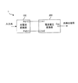
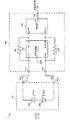
図1は、第1実施例に係る光検出装置の全体構成を示すブロック図であり、図2は、第1実施例に係る光検出装置の構成を示すブロック図である。 FIG. 1 is a block diagram showing the overall configuration of the photodetector according to the first embodiment, and FIG. 2 is a block diagram showing the configuration of the photodetector according to the first embodiment.
図1及び図2において、第1実施例に係る光検出装置1は、外部から入力される入力光に含まれる信号光成分を検出するための光検出装置であり、光電流変換部100と、電流電圧変換部200とを備えている。入力光は、例えば、レーザー光が被検体(例えば人間の指など)によって例えば反射、散乱等された光であり、被検体に係る情報を示す信号光成分(例えば、被検体における例えば反射、散乱等による変調成分)を含んでいる。
1 and 2, the
図2において、光電流変換部100は、受光素子110及び120と、端子Pd1及びPd2とを有している。尚、受光素子110は、本発明に係る「第1光電変換素子部」の一例であり、受光素子120は、本発明に「第2光電変換素子部」の一例である。
In FIG. 2, the
受光素子110及び120の各々は、例えばPINダイオード(P-Intrinsic-N Diode)等のフォトダイオードであり、入力光を受光し、受光した入力光の光量に応じて電流を出力する。受光素子110及び120は、受光素子110のカソード(言い換えれば、受光素子110のN型半導体)と受光素子120のアノード(言い換えれば、受光素子110のP型半導体)とが互いに接続され且つ受光素子110のアノード(言い換えれば、受光素子110のP型半導体)と受光素子120のカソード(言い換えれば、受光素子120のN型半導体)とが互いに接続されるように、並列接続されている。受光素子110のアノード及び受光素子120のカソードは、端子Pd1に接続され、受光素子110のカソード及び受光素子120のアノードは、端子Pd2に接続されている。受光素子110及び120がこのように並列接続されているので、光電流変換部100は、受光素子110が出力する電流Idt1と受光素子120が出力する電流Idt2と差分電流を検出電流Idtとして端子Pd1から出力することができる。
Each of the
端子Pd1及びPd2は、後述する電流電圧変換部200の入力端子In1及びIn2にそれぞれ接続されている。
The terminals Pd1 and Pd2 are respectively connected to input terminals In1 and In2 of a current-
電流電圧変換部200は、入力端子In1及びIn2と、オペアンプ210と、帰還抵抗Rfと、出力端子Outとを有している。電流電圧変換部200は、入力端子In1に入力される電流を電圧信号に変換して出力するトランスインピーダンスアンプ(電流−電圧変換増幅器)として構成されている。電流電圧変換部200は、光電流変換部100から入力端子In1に入力される検出電流Idtを電圧信号に変換して出力端子Outから光検出信号として出力する。
The current-
入力端子In1は、オペアンプ210の反転入力端子(−)に接続されている。入力端子In2は、オペアンプ210の非反転入力端子(+)に接続されている。入力端子In2及びオペアンプ210の非反転入力端子は接地されている(即ち、例えばグランド(GND)電位等の基準電位に接続されている)。
The input terminal In1 is connected to the inverting input terminal (−) of the
帰還抵抗Rfは、オペアンプ210の出力端子とオペアンプ210の反転入力端子との間に接続されており、負帰還を施すと共に電流を電圧に変換する。帰還抵抗Rfによって負帰還が施されることにより、オペアンプ210の反転入力端子と非反転入力端子との電位差は殆どゼロになっている(即ち、いわゆる「イマジナルショート(仮想短絡)」が成立している)。
The feedback resistor Rf is connected between the output terminal of the
出力端子Outは、オペアンプ210の出力端子に接続されている。出力端子Outは、オペアンプ210から出力される電圧信号を光検出信号として出力する。
The output terminal Out is connected to the output terminal of the
次に、本実施例に係る光検出装置の動作について、図2を参照して説明する。 Next, the operation of the photodetecting device according to the present embodiment will be described with reference to FIG.
図2において、光検出装置1の動作時には、入力光が受光素子110及び120の各々によって受光されると、受光素子110及び120の各々から入力光の光量に応じた電流が出力される。即ち、受光素子110は、受光した入力光の光量に応じて電流Idt1を出力し、受光素子120は、受光した入力光の光量に応じて電流Idt2を出力する。すると、前述したように、受光素子110及び120は、受光素子110のカソードと受光素子120のアノードとが互いに接続され且つ受光素子110のアノードと受光素子120のカソードとが互いに接続されるように、並列接続されているので、受光素子110から出力される電流Idt1と受光素子120から出力される電流Idt2との差分電流が端子Pd1から検出電流Idtとして出力される。
In FIG. 2, when input light is received by each of the
ここで、入力光には信号光成分(例えば、被検体における例えば反射、散乱等による変調成分)と定常成分(例えば、被検体に照射されるレーザー光の光量に応じた成分やノイズ成分)とが含まれる。よって、受光素子110が出力する電流Idt1と受光素子120が出力する電流Idt2とには、それぞれ、入力光に含まれる信号光成分に相当する電流成分であるAC成分と、入力光に含まれる定常光成分に相当する電流成分であるDC成分とが含まれる。受光素子110に入力される入力光の信号光成分と、受光素子120に入力される入力光の信号光成分とは、受光素子110が配置された位置と受光素子120が配置された位置とが互いに異なるため、光学的経路が互いに異なる。そのため信号光成分に相当する電流成分は互いに相関の低い信号となる。よって、受光素子110が出力する電流Idt1のAC成分(即ち、信号光成分に相当する電流成分)と、受光素子120が出力する電流Idt2のAC成分とは、互いに相関が低い。即ち、電流Idt1及びIdt2のAC成分は、互いに位相や振幅や周波数が異なる非同相成分を多く含む(言い換えれば、互いに相関が低い無相関成分である)。一方、受光素子110が出力する電流Idt1のDC成分(即ち、定常光成分に相当する電流成分)と、受光素子120が出力する電流Idt2のDC成分とは、例えば受光面積を等しく設計した場合、互いの振幅はほぼ等しい。即ち、電流Idt1及びIdt2のDC成分は、互いに同相成分(言い換えれば、互いに相関が強い相関成分)である。
Here, the input light includes a signal light component (for example, a modulation component due to reflection, scattering, etc. in the subject) and a stationary component (for example, a component or a noise component according to the amount of laser light applied to the subject). Is included. Therefore, the current Idt1 output from the
よって、図3に示すように、受光素子110から出力される電流Idt1と受光素子120から出力される電流Idt2との差分電流である検出電流Idtは、電流Idt1及びIdt2のAC成分に比較して増加すると共にDC成分が低減或いは除去された電流となる。互いに無相関成分を多く含む信号同士の減算は、ランダム信号の減算と等価であり、減算後信号パワーは増加する。尚、図3は、検出電流Idt及びオペアンプ210の出力電圧Voutの各々の一例を示す波形図である。
Therefore, as shown in FIG. 3, the detection current Idt, which is the difference current between the current Idt1 output from the
即ち、本実施例に係る光電流変換部100によれば、受光素子110が出力する電流Idt1のDC成分と、受光素子120が出力する電流Idt2のDC成分とを相殺させることができ、入力光に含まれる信号光成分に相当するAC成分を主として含む検出電流Idtを出力することができる。
That is, according to the
従って、電流電圧変換部200によって検出電流Idtを増幅して電圧信号に変換する際の利得を高めることができる。言い換えれば、本実施例によれば、前述したように、受光素子110が出力する電流Idt1のDC成分と、受光素子120が出力する電流Idt2のDC成分とが相殺されており、検出電流IdtにはDC成分が殆ど或いは全く含まれていないので、例えば検出電流Idtに含まれるDC成分が比較的大きい場合に発生し得る、電流電圧変換部200に含まれるオペアンプ210の飽和現象の発生を回避しつつ、電流電圧変換部200による増幅の利得を大きくすることができる。言い換えれば、図3において、オペアンプ210の出力電圧Voutの最大値とオペアンプ210の飽和電圧Vsとの差ΔV1を比較的大きく維持しつつ、電流電圧変換部200による増幅の利得を大きくすることができる。
Therefore, the gain at the time of converting the detection current Idt into a voltage signal by the current-
更に、本実施例によれば、前述したように、光電流変換部100は、入力光に含まれる信号光成分に相当するAC成分を主として含む電流を、検出電流Idtとして出力することができるので、電流電圧変換部200が出力する光検出信号におけるS/N比を向上させることができる。即ち、本実施例によれば、受光素子110が出力する電流Idt1と受光素子120が出力する電流Idt2とから、入力光に定常光成分として含まれるノイズ成分(例えばレーザー光源のゆらぎに起因するノイズ成分)に相当するDC成分を低減或いは除去して、信号成分に相当するAC成分を主として含む検出電流Idtを出力するので、電流電圧変換部200が出力する光検出信号におけるS/N比を向上させることができる。
Furthermore, according to the present embodiment, as described above, the
加えて、本実施例によれば、前述したように、オペアンプ210の反転入力端子と非反転入力端子との電位差が殆どゼロになるイマジナルショートが成立している。よって、オペアンプ210の反転入力端子に入力端子In1を介して接続されている端子Pd1と、オペアンプ210の非反転入力端子に入力端子In2を介して接続されている端子Pd2との電位差も殆どゼロであり、受光素子110及び120の各々をゼロバイアスの状態(即ち、逆バイアス電圧が殆ど或いは全く印加されない状態)、即ち、いわゆる発電モードで動作させることができる。従って、受光素子110及び120に発生する暗電流を低減或いは無くすことができる。これにより、暗電流のゆらぎによるノイズ電流を低下させることができ、電流電圧変換部200が出力する光検出信号におけるS/N比を向上させることができる。
In addition, according to the present embodiment, as described above, an imaginary short is established in which the potential difference between the inverting input terminal and the non-inverting input terminal of the
本実施例によれば、入力光に定常光成分として含まれるDC成分を低減或いは除去できるので、電流電圧変換部200において、飽和現象を回避しつつ、入力である検出電流Idtに対する出力である出力電圧Voutの比、即ち変換ゲインを高くできるので、S/N比を向上させることができる。
According to the present embodiment, since the DC component included in the input light as a steady light component can be reduced or removed, in the current-
具体的には、図2における帰還抵抗Rfの抵抗値を高くしても、オペアンプ210の飽和現象を回避できる。電流電圧変換部200が発生するノイズの主要成分のひとつとして、帰還抵抗Rfの熱雑音が良く知られている。熱雑音は、帰還抵抗Rfの抵抗値の平方根に比例する。一方、変換ゲインは、帰還抵抗Rfの抵抗値に比例するので、帰還抵抗Rfの抵抗値を高くするとS/N比は、帰還抵抗Rfの抵抗値の平方根倍で改善される。しかし、従来の単一フォトダイオード構成で帰還抵抗Rfの抵抗値を高くすると、DC成分によりオペアンプ210が飽和してしまう。仮にオペアンプ210が飽和した場合、信号成分は出力されなくなり、致命的な不具合が生じる。一方、本実施例によれば、検出電流Idtの段階でDC成分を低減或いは除去できるので、帰還抵抗Rfの抵抗値を高くしてもオペアンプ210は飽和しない。従って、本実施例によれば、オペアンプ210の飽和回避と、高変換ゲインによる高S/N化の両立が可能となる。
Specifically, even if the resistance value of the feedback resistor Rf in FIG. 2 is increased, the saturation phenomenon of the
以上説明したように、本実施例に係る光検出装置1によれば、電流電圧変換部200が出力する光検出信号におけるS/N比を向上させることができる。この結果、入力光に含まれる信号光成分を精度良く検出することが可能となる。
As described above, according to the
<第2実施例>
第2実施例に係る光検出装置について、図4を参照して説明する。<Second embodiment>
A photodetecting device according to the second embodiment will be described with reference to FIG.
図4は、第2実施例に係る光検出装置の構成を示すブロック図である。尚、図4において、図2に示した第1実施例に係る構成要素と同様の構成要素に同一の参照符合を付し、それらの説明は適宜省略する。 FIG. 4 is a block diagram illustrating a configuration of the photodetecting device according to the second embodiment. In FIG. 4, the same reference numerals are given to the same components as those in the first embodiment shown in FIG. 2, and the description thereof will be omitted as appropriate.
図4において、第2実施例に係る光検出装置1bは、前述した第1実施例における光電流変換部100に代えて光電流変換部100bを備える点で、前述した第1実施例に係る光検出装置1と異なり、その他の点については、前述した第1実施例に係る光検出装置1と概ね同様に構成されている。
In FIG. 4, the
図4において、光電流変換部100bは、受光素子110b及び120bと、端子Pd1b及びPd2bとを有している。尚、受光素子110bは、本発明に係る「第1光電変換素子部」の一例であり、受光素子120bは、本発明に「第2光電変換素子部」の一例である。
In FIG. 4, the
受光素子110b及び120bの各々は、例えばPINダイオード等のフォトダイオードであり、入力光を受光し、受光した入力光の光量に応じて電流を出力する。受光素子110b及び120bは、互いにカソード同士が接続されるように、直列接続されている。受光素子110bのアノードは、端子Pd1bに接続され、受光素子120bのアノードは、端子Pd2bに接続されている。受光素子110b及び120bがこのように直列接続されているので、光電流変換部100bは、受光素子110bが出力する電流Idt1bと受光素子120bが出力する電流Idt2bと差分電流を検出電流Idtbとして端子Pd1bから出力することができる。
Each of the
端子Pd1b及びPd2bは、電流電圧変換部200の入力端子In1及びIn2にそれぞれ接続されている。
The terminals Pd1b and Pd2b are connected to the input terminals In1 and In2 of the current-
このように構成された光検出装置1bによって、前述した第1実施例に係る光検出装置1によって得られる利益と同様の利益を得ることができる。即ち、受光素子110bが出力する電流Idt1bのDC成分と、受光素子120bが出力する電流Idt2bのDC成分とを相殺させることができ、入力光に含まれる信号光成分に相当するAC成分を主として含む検出電流Idtbを出力することができる。この結果、電流電圧変換部200が出力する光検出信号におけるS/N比を向上させることができる。
By the
<第3実施例>
第3実施例に係る光検出装置について、図5及び図6を参照して説明する。<Third embodiment>
A photodetecting device according to a third embodiment will be described with reference to FIGS.
図5は、第3実施例に係る光検出装置の構成を示すブロック図である。 FIG. 5 is a block diagram showing the configuration of the photodetecting device according to the third embodiment.
図5において、第3実施例に係る光検出装置1cは、外部から入力される入力光に含まれる信号光成分を検出するための光検出装置であり、光電流変換部100cと、電流電圧変換部200cとを備えている。入力光は、例えば、レーザー光が被検体(例えば人間の指など)によって例えば反射、散乱等された光であり、被検体に係る情報を示す信号光成分(例えば、被検体における例えば反射、散乱等による変調成分)を含んでいる。
In FIG. 5, a photodetection device 1c according to the third embodiment is a photodetection device for detecting a signal light component included in input light input from the outside, and includes a
図5において、光電流変換部100cは、受光素子110c及び120cと、端子Pd1c及びPd2cとを有している。尚、受光素子110cは、本発明に係る「第1光電変換素子部」の一例であり、受光素子120cは、本発明に「第2光電変換素子部」の一例である。
In FIG. 5, the
受光素子110c及び120cの各々は、例えばPINダイオード等のフォトダイオードであり、入力光を受光し、受光した入力光の光量に応じて電流を出力する。受光素子110c及び120cは、互いにアノード同士が接続されるように、直列接続されている。受光素子110cのカソードは、端子Pd1cに接続され、受光素子120cのカソードは、端子Pd2cに接続されている。受光素子110c及び120cがこのように直列接続されているので、光電流変換部100cは、受光素子110cが出力する電流Idt1cと受光素子120cが出力する電流Idt2cとの差分電流(Idt2c−Idt1c)を検出電流Idtcとして端子Pd1cから出力することができる。また、光電流変換部100cは、端子Pd1から出力する検出電流Idtcの極性が反転された電流(−Idtc)を端子Pd2cから出力することができる。
Each of the
端子Pd1c及びPd2cは、電流電圧変換部200cの入力端子In1c及びIn2cにそれぞれ接続されている。
The terminals Pd1c and Pd2c are connected to the input terminals In1c and In2c of the current-
このように構成された光電流変換部200cによれば、受光素子110cが出力する電流Idt1cのDC成分と、受光素子120cが出力する電流Idt2cのDC成分とを相殺させることができ、入力光に含まれる信号光成分に相当するAC成分を主として含む検出電流Idtcを出力することができる。この結果、電流電圧変換部200cが出力する光検出信号におけるS/N比を向上させることができる。
According to the
電流電圧変換部200cは、入力端子In1c及びIn2cと、本発明に係る「全差動増幅器」の一例としての全差動アンプ230と、帰還抵抗Rf1及びRf2と、増幅器240と、出力端子Outとを有している。全差動アンプ230は、入力端子In1cに入力される電流Idtcを電圧信号−Rf1・Idtcに変換し、出力端子Out−から出力する。同時に、全差動アンプ230は、入力端子In2cに入力される電流−Idtcを電圧信号Rf2・Idtcに変換し、出力端子Out+から出力する。即ち、全差動アンプ230は、入力端子In1及びIn2に入力される電流を、それぞれ独立して電流電圧変換し、差動出力するトランスインピーダンスアンプとして構成されている。
電流電圧変換部200cは、光電流変換部100cから入力端子In1cに入力される検出電流Idtcを電圧信号に変換して出力端子Outから光検出信号として出力する。The current-
The current-
全差動アンプ230は、入力端子In1cに接続された入力端子In+と、入力端子In2cに接続された入力端子In−と、出力端子Out−と、出力端子Out+とを有する全差動増幅器である。基準電位は、基準電位端子Vrefを介して入力される。出力端子Out−及びOut+は、後述する増幅器240の入力端子In−及びIn+にそれぞれ接続されている。
The fully
帰還抵抗Rf1は、全差動アンプ230の入力端子In+と全差動アンプ230の出力端子Out−との間に接続されており、負帰還を施すと共に電流を電圧に変換する。帰還抵抗Rf2は、全差動アンプ230の入力端子In−と全差動アンプ230の出力端子Out+との間に接続されており、負帰還を施すと共に電流を電圧に変換する。帰還抵抗Rf1及びRf2によって負帰還が施されることにより、全差動アンプ230の入力端子In+と基準電位端子Vrefとの電位差は殆どゼロになっている。同様に入力端子In−との基準電位端子Vrefとの電位差は殆どゼロになっている。その結果、入力端子In+と入力端子In−は殆ど同電位になる。よって、全差動アンプ230の入力端子In+に入力端子In1cを介して接続されている端子Pd1cと、全差動アンプ230の入力端子In−に入力端子In2cを介して接続されている端子Pd2cとの電位差も殆どゼロであり、受光素子110c及び120cの各々をゼロバイアスの状態、即ち、いわゆる発電モードで動作させることができる。従って、受光素子110c及び120cに発生する暗電流を低減或いは無くすことができる。これにより、暗電流のゆらぎによるノイズ電流を低下させることができ、電流電圧変換部200cが出力する光検出信号におけるS/N比を向上させることができる。
The feedback resistor Rf1 is connected between the input terminal In + of the fully
増幅器240は、入力端子In−から入力される電圧信号−Rf1・Idtcと、入力端子In+から入力される電圧信号Rf2・Idtcとの電位差2・Rf・Idtc(Rf1=Rf2=Rfに選ぶ)を増幅して出力する増幅器である。増幅器240の出力端子は、電流電圧変換部200cの出力端子Outに接続されている。
The
図6は、増幅器240の構成を示す回路図である。
FIG. 6 is a circuit diagram showing a configuration of the
図6において、増幅器240は、計装アンプとして構成されており、オペアンプOP1、OP2及びOP3と、帰還抵抗R2、R3及びR6と、共通入力抵抗R1と、入力抵抗R4、R5及びR7とを備えている。
In FIG. 6, an
増幅器240の入力端子In−は、オペアンプOP1の非反転入力端子(+)に接続されている。増幅器240の入力端子In+は、オペアンプOP2の非反転入力端子(+)に接続されている。オペアンプOP1及びOP2は、帰還抵抗R2及びR3によってそれぞれ負帰還が施される。
The input terminal In− of the
帰還抵抗R2とR3とは、等しい抵抗値に設定されている。 The feedback resistors R2 and R3 are set to equal resistance values.
共通入力抵抗R1は、オペアンプOP1の反転入力端子とオペアンプOP2の反転入力端子との間に接続されている。尚、共通入力抵抗R1は、利得を可変とするために可変抵抗として機能してもよい。 The common input resistor R1 is connected between the inverting input terminal of the operational amplifier OP1 and the inverting input terminal of the operational amplifier OP2. The common input resistor R1 may function as a variable resistor in order to make the gain variable.
オペアンプOP1の出力端子は、入力抵抗R4を介して、オペアンプOP3の反転入力端子に接続されている。オペアンプOP2の出力端子は、入力抵抗R5を介して、オペアンプOP3の非反転入力端子に接続されている。入力抵抗R5とオペアンプOP3の非反転入力端子との間には、入力抵抗R7の一方の端子が接続されている。入力抵抗R7の他方の端子は、例えばGND電位である基準電位Vrefに接続されている。オペアンプOP2から出力される電圧は、入力抵抗R5及びR7によって分圧されオペアンプOP3の非反転入力端子に入力される。 The output terminal of the operational amplifier OP1 is connected to the inverting input terminal of the operational amplifier OP3 via the input resistor R4. The output terminal of the operational amplifier OP2 is connected to the non-inverting input terminal of the operational amplifier OP3 via the input resistor R5. One terminal of the input resistor R7 is connected between the input resistor R5 and the non-inverting input terminal of the operational amplifier OP3. The other terminal of the input resistor R7 is connected to a reference potential Vref which is, for example, a GND potential. The voltage output from the operational amplifier OP2 is divided by the input resistors R5 and R7 and input to the non-inverting input terminal of the operational amplifier OP3.
入力抵抗R4とR5とは、等しい抵抗値に設定されている。 The input resistors R4 and R5 are set to the same resistance value.
オペアンプOP3は、帰還抵抗R6によって負帰還が施される。オペアンプOP3の出力端子は、電流電圧変換部200cの出力端子Outに接続されている。
The operational amplifier OP3 is negatively fed back by the feedback resistor R6. The output terminal of the operational amplifier OP3 is connected to the output terminal Out of the current-
帰還抵抗R6と入力抵抗R7とは、等しい抵抗値に設定されている。 The feedback resistor R6 and the input resistor R7 are set to the same resistance value.
このように構成された増幅器240によれば、全差動アンプ230の出力端子Out−及びOut+からそれぞれ出力される2つの電圧信号における同相成分(例えばハムノイズなど)を、ノイズとして除去することができる。更に、全差動アンプ230の出力端子Out−及びOut+からそれぞれ出力される2つの電圧信号は、検出電流Idtcに応じて差動出力されており、極性が互いに異なる2つの差動信号である。よって、増幅器240の入力端子In+及びIn−には、検出した光の信号成分は逆相で入力される。これにより、増幅器240が光検出信号として出力する電圧信号から例えばハムノイズ等の同相成分を、ノイズとして除去することができる。加えて、検出した光の信号成分は逆相なので、増幅器240によって増幅されて、光検出信号として出力される。この結果、光検出信号において、ノイズ成分を低下させると共に信号成分を増加させることができるので、S/Nを顕著に向上させることができる。
According to the
<第4実施例>
第4実施例に係る光検出装置について、図7を参照して説明する。<Fourth embodiment>
A light detection apparatus according to the fourth embodiment will be described with reference to FIG.
第4実施例に係る光検出装置は、図5及び図6を参照して前述した第3実施例における増幅器240に代えて増幅器240dを備える点で、前述した第3実施例に係る光検出装置1cと異なり、その他の点については、前述した第3実施例に係る光検出装置1cと概ね同様に構成されている。
The light detection apparatus according to the fourth embodiment is provided with an
図7は、第4実施例に係る増幅器の構成を示す回路図である。尚、図7において、図5及び図6に示した第3実施例に係る構成要素と同様の構成要素に同一の参照符合を付し、それらの説明は適宜省略する。 FIG. 7 is a circuit diagram showing a configuration of an amplifier according to the fourth embodiment. In FIG. 7, the same components as those in the third embodiment shown in FIGS. 5 and 6 are denoted by the same reference numerals, and the description thereof will be omitted as appropriate.
図7において、本実施例に係る増幅器240dは、オペアンプOP1及びOP2と、帰還抵抗R2及びR3と、共通入力抵抗R1と、ローパスフィルタ(即ち、低域通過フィルタ)LPF1及びLPF2と、AD(Analog to Digital)変換器ADC1及びADC2とを備えている。
In FIG. 7, an
図5及び図6を参照して前述した第3実施例に係る増幅器240は、シングルエンドの信号であると共にアナログ信号として光検出信号を出力することが可能に構成されている。これに対して、図7に示すように、本実施例に係る増幅器240dは、極性の異なる2つの差動信号を光検出信号DtOut1及びDtOut2として出力するように構成されている。加えて、光検出信号DtOut1及びDtOut2は、ローパスフィルタLPF1及びLPF2並びにAD変換器ADC1及びADC2を介してデジタル信号として出力される。増幅器240dによれば、オペアンプOP1の出力信号は、アンチエリアスフィルタ(即ち、AD変換器によるサンプリングによって発生するエリアシングノイズを除去可能なフィルタ)としてのローパスフィルタLPF1を介してAD変換機ADC1に入力され、オペアンプOP2の出力信号は、アンチエリアスフィルタとしてのローパスフィルタLPF2を介してAD変換機ADC2に入力される。よって、光検出信号DtOut1及びDtOut2の各々のS/N比を高めることが可能である。AD変換器ADC1及びADC2の出力信号である量子化された光検出信号DtOut1及びDtOut2は、例えばDSP(Digital Signal Processor)等のデジタル信号処理装置等の信号処理装置(不図示)によって減算処理が実行されてよい。
The
以上の結果、本実施例によれば、光検出信号DtOut1及びDtOut2は、量子化されているので、例えば通信網を介して伝送する場合における、外界環境からのノイズに強くなる。よって、光検出信号の長距離伝送を実現することが可能となる。 As a result, according to the present embodiment, since the photodetection signals DtOut1 and DtOut2 are quantized, for example, when the signal is transmitted via a communication network, it becomes strong against noise from the external environment. Therefore, it is possible to realize long-distance transmission of the light detection signal.
<第5実施例>
第5実施例に係る血流計測装置について、図8を参照して説明する。<Fifth embodiment>
A blood flow measuring apparatus according to a fifth embodiment will be described with reference to FIG.
図8は、第5実施例に係る血流計測装置の構成を示すブロック図である。尚、図8において、図1及び図2に示した第1実施例に係る構成要素と同様の構成要素に同一の参照符合を付し、それらの説明は適宜省略する。 FIG. 8 is a block diagram showing the configuration of the blood flow measurement device according to the fifth embodiment. In FIG. 8, the same components as those in the first embodiment shown in FIGS. 1 and 2 are denoted by the same reference numerals, and description thereof will be omitted as appropriate.
図8において、本実施例に係る血流計測装置1001は、本発明に係る「流体計測装置」の一例であり、生体である被検体900の血流量を計測するための装置である。
In FIG. 8, a blood
血流計測装置1001は、レーザー駆動装置2と、半導体レーザー3と、図1及び図2を参照して前述した第1実施例に係る光検出装置1と、信号処理部5とを備えている。尚、レーザー駆動装置2及び半導体レーザー3は、本発明に係る「照射部」の一例であり、信号処理部5は、本発明に係る「算出部」の一例である。
The blood
図8において、レーザー駆動装置2によって半導体レーザー3が駆動されることにより、半導体レーザー3からの光が被検体900に照射される。被検体900に照射された光は、被検体900の毛細血管内のヘモクロビンにより反射或いは散乱される。このように被検体900において反射或いは散乱された光は、光検出装置1の光電流変換部100(より具体的には、図2を参照して前述した受光素子110及び120)に入射される。入射された光に応じて光電流変換部100から検出電流Idtが出力される。検出電流Idtは、電流電圧変換部200によって電圧信号に変換されて、光検出信号として信号処理部5に入力される。信号処理部5は、入力された光検出信号に基づいて血流量を算出し、血流量を示すデジタル信号を血流量検出信号として出力する。
In FIG. 8, the semiconductor laser 3 is driven by the
ここで特に、血流計測装置1001は、前述した第1実施例に係る光検出装置1を備えているので、S/Nが高い光検出信号に基づいて、信号処理部5によって血流量を算出することができる。よって、血流量を正確に算出することができる。
Here, in particular, the blood
尚、血流計測装置は、前述した第1実施例に係る光検出装置1と同様にそれぞれ構成された2つの光検出装置と、該2つの光検出装置からそれぞれ出力される光検出信号の差分に基づいて血流量を算出し、血流量を示すデジタル信号を血流量検出信号として出力する信号処理部とを更に備えてもよい。このように構成すれば、例えばハムノイズ等の同相成分をより確実に除去することができ、より正確に、血流量を算出することができる。
The blood flow measuring device includes two light detection devices each configured in the same manner as the
<第6実施例>
第6実施例に係る血流計測装置について、図9を参照して説明する。<Sixth embodiment>
A blood flow measurement apparatus according to the sixth embodiment will be described with reference to FIG.
図9は、第6実施例に係る血流計測装置の構成を示すブロック図である。尚、図9において、図4に示した第2実施例に係る構成要素及び図8に示した第5実施例に係る構成要素と同様の構成要素に同一の参照符合を付し、それらの説明は適宜省略する。 FIG. 9 is a block diagram illustrating the configuration of the blood flow measurement device according to the sixth embodiment. In FIG. 9, the same reference numerals are assigned to the same constituent elements as the constituent elements according to the second embodiment shown in FIG. 4 and the constituent elements according to the fifth embodiment shown in FIG. Are omitted as appropriate.
図9において、本実施例に係る血流計測装置1002は、本発明に係る「流体計測装置」の一例であり、生体である被検体900の血流量を計測するための装置である。
In FIG. 9, a blood
血流計測装置1002は、レーザー駆動装置2と、半導体レーザー3と、光検出装置1gと、信号処理部5gとを備えている。
The blood
光検出装置1gは、光電流変換部100b及び電流電圧変換部200gを備えている。
The
光電流変換部100bは、互いにカソード同士が接続されるように、直列接続された受光素子110b及び120bを有している。受光素子110bのアノードは、端子Pd1bを介して電流電圧変換部200gの入力端子In1に接続され、受光素子120bのアノードは、端子Pd2bを介して電流電圧変換部200gの入力端子In2に接続されている。
The
本実施例では特に、受光素子110b及び120b間にバイアス印加選択素子300の一端が接続されている。バイアス印加選択素子300は、コントローラ400からの指令に基づいて、受光素子110b及び120bにバイアス電圧を印加するか否かを選択する。バイアス印加選択素子300は、アナログスイッチSW1から構成されている。アナログスイッチSW1の一端は、受光素子110bと120bとの間(即ち、受光素子110bと120bとの接続点)に接続され、アナログスイッチSW1の他端は、例えばGND電位等のバイアス電位に接続されている。バイアス印加選択素子300は、コントローラ400からの指令に応じて、アナログスイッチSW1のオンオフを切り替えることで、受光素子110b及び120bにバイアス電圧を印加するか否かを選択する。尚、バイアス印加選択素子300及びコントローラ400は、本発明に係る「バイアス電圧印加手段」の一例である。
In the present embodiment, in particular, one end of the bias
電流電圧変換部200gは、図7を参照して前述した光検出装置が備える電流電圧変換部と概ね同様に構成されている。即ち、電流電圧変換部200gは、全差動アンプ230(図5参照)、帰還抵抗Rf1及びRf2(図5参照)並びに増幅器240d(図7参照)を備えている。電流電圧変換部200gは、出力端子Out1及びOut2から光検出信号DtOut1及びDtOut2をそれぞれ出力する。
The current-
信号処理部5gは、入力された光検出信号DtOut1及びDtOut2に基づいて血流量を算出し、血流量を示すデジタル信号を血流量検出信号として出力する。信号処理部5gは、コントローラ400からの指令に基づいて、受光素子110b及び120bにバイアスが印加されるバイアス印加時(即ち、アナログスイッチSW1がオン状態とされたとき)と、受光素子110b及び120bにバイアスが印加さない開放時(即ち、アナログスイッチSW1がオフ状態とされたとき)とで、信号処理の内容を変更する。
The signal processing unit 5g calculates a blood flow based on the input light detection signals DtOut1 and DtOut2, and outputs a digital signal indicating the blood flow as a blood flow detection signal. Based on a command from the
具体的には、バイアス印加時には、信号処理部5gは、入力される光検出信号DtOut1及びDtOut2を加算することにより、DC光パワー成分を算出する。一方、開放時には、入力される光検出信号DtOut1及びDtOut2を減算することにより、例えばビート信号等の信号光成分のパワースペクトルを算出し、これに基づいて被検体900の血流量を算出する。更に、信号処理部5gは、開放時に算出した血流量を、バイアス印加時に算出したDC光パワー成分で除算することで規格化を行う。これにより、半導体レーザー3から出射される光にパワー変動が生じたとしても被検体900の血流量を精度良く測定することが可能となる。 Specifically, at the time of bias application, the signal processing unit 5g calculates the DC light power component by adding the input photodetection signals DtOut1 and DtOut2. On the other hand, at the time of opening, the input light detection signals DtOut1 and DtOut2 are subtracted to calculate the power spectrum of a signal light component such as a beat signal, and the blood flow rate of the subject 900 is calculated based on this. Furthermore, the signal processing unit 5g performs normalization by dividing the blood flow volume calculated at the time of opening by the DC light power component calculated at the time of bias application. As a result, even if power fluctuations occur in the light emitted from the semiconductor laser 3, the blood flow rate of the subject 900 can be accurately measured.
<第7実施例>
第7実施例に係る光検出装置について、図10を参照して説明する。<Seventh embodiment>
A photodetecting device according to the seventh embodiment will be described with reference to FIG.
図10は、第7実施例に係る光検出装置の構成を示す回路図である。尚、図10において、図2に示した第1実施例に係る構成要素と同様の構成要素に同一の参照符合を付し、それらの説明は適宜省略する。 FIG. 10 is a circuit diagram showing a configuration of the photodetector in accordance with the seventh embodiment. In FIG. 10, the same reference numerals are given to the same components as those in the first embodiment shown in FIG. 2, and the description thereof will be omitted as appropriate.
図10において、第7実施例に係る光検出装置1hは、受光素子130及び該受光素子130から出力される電流を電圧に変換する電流電圧変換部分203を更に備える点で、前述した第1実施例に係る光検出装置1と異なり、その他の点については、前述した第1実施例に係る光検出装置1と概ね同様に構成されている。尚、受光素子130は、本発明に係る「第3光電変換素子部」の一例であり、電流電圧変換部分203は、本発明に係る「第2電流電圧変換部」の一例である。
In FIG. 10, the photodetector 1h according to the seventh embodiment includes the
図10において、第7実施例に係る光検出装置1hは、光電流変換部100hと、電流電圧変換部200hとを備えている。
In FIG. 10, the photodetector 1h according to the seventh embodiment includes a
光電流変換部100hは、前述した第1実施例における光電流変換部100と同様に、並列接続された受光素子110及び120と、端子Pd1及びPd2とを有している。更に、光電流変換部100hは、受光素子110及び120とは別個に設けられた受光素子130と、端子Pd1h及びPd2hとを有している。受光素子130は、例えばPINダイオード等のフォトダイオードであり、入力光を受光し、受光した入力光の光量に応じて電流を出力する。受光素子130のカソードは、端子Pd1hに接続され、受光素子130のアノードは、端子Pd2hに接続されている。
The
端子Pd1h及びPd2hは、後述する電流電圧変換部200hの入力端子In1h及びIn2hにそれぞれ接続されている。
The terminals Pd1h and Pd2h are respectively connected to input terminals In1h and In2h of a current-
電流電圧変換部200hは、前述した第1実施例における光電流変換部と概ね同様に、入力端子In1及びIn2と、オペアンプ210と、帰還抵抗Rfと、出力端子OutAとを有している。尚、出力端子OutAは、オペアンプ210の出力端子に接続されている。出力端子OutAは、オペアンプ210から出力される電圧信号を光検出信号DtOutAとして出力する。
The current-
更に、電流電圧変換部200hは、受光素子130から出力される電流を電圧に変換する電流電圧変換部分203を有している。電流電圧変換部分203は、入力端子In1h及びIn2hと、オペアンプ210hと、帰還抵抗Rfhと、出力端子OutBとを有している。
Furthermore, the current-
入力端子In1hは、オペアンプ210hの反転入力端子(−)に接続されている。入力端子In2hは、オペアンプ210hの非反転入力端子(+)に接続されている。入力端子In2h及びオペアンプ210hの非反転入力端子は接地されている。
The input terminal In1h is connected to the inverting input terminal (−) of the
帰還抵抗Rfhは、オペアンプ210hの出力端子とオペアンプ210hの反転入力端子との間に接続されており、負帰還を施すと共に電流を電圧に変換する。帰還抵抗Rfhによって負帰還が施されることにより、オペアンプ210hの反転入力端子と非反転入力端子との電位差は殆どゼロになっている(即ち、いわゆるイマジナルショートが成立している)。
The feedback resistor Rfh is connected between the output terminal of the
出力端子OutBは、オペアンプ210hの出力端子に接続されている。出力端子OutBは、オペアンプ210hから出力される電圧信号を光検出信号DtOutBとして出力する。
The output terminal OutB is connected to the output terminal of the
このように本実施例では特に、光検出装置1hは、受光素子130及び該受光素子130から出力される電流を電圧に変換する電流電圧変換部分203を備えるので、受光素子130が出力する電流Idt3に基づいて、入力光の定常光成分に相当する信号を光検出信号DtOutBとして出力することができる。よって、互いに並列接続された受光素子110及び120からの検出電流Idtに基づく光検出信号DtOutA(即ち、入力光の信号光成分に相当する信号)を、光検出信号DtOutB(即ち、入力光の定常光成分(DC光成分)に相当する信号)で除算することにより信号の規格化を行うことができる。よって、光源から出射される光にパワー変動が生じたとしても入力光に含まれる信号成分を精度良く検出することができる。
As described above, particularly in the present embodiment, the light detection device 1h includes the
本発明は、上述した実施例に限られるものではなく、特許請求の範囲及び明細書全体から読み取れる発明の要旨或いは思想に反しない範囲で適宜変更可能であり、そのような変更を伴う光検出装置及び流体計測装置もまた本発明の技術的範囲に含まれるものである。 The present invention is not limited to the above-described embodiments, and can be appropriately changed without departing from the gist or concept of the invention that can be read from the claims and the entire specification. In addition, fluid measuring devices are also included in the technical scope of the present invention.
1、1b、1c、1g、1h 光検出装置
2 レーザー駆動装置
3 半導体レーザー
5、5g 信号処理部
100、100b、100c、100g、100h 光電流変換部
110、120、110b、120b、110c、120c 受光素子
200、200c、200g、200h 電流電圧変換部
210、210h オペアンプ
230 全差動アンプ
240、240d 増幅器
300 バイアス印加選択素子
400 コントローラ
1001、1002 血流計測装置
Rf、Rfh、Rf1、Rf2 帰還抵抗
SW1 アナログスイッチ1, 1b, 1c, 1g,
Claims (5)
前記入力光を電流に夫々変換して出力する第1及び第2光電変換素子部を含んでなり、前記第1光電変換素子部が出力する電流と前記第2光電変換素子部が出力する電流との差分電流を検出電流として出力する光電流変換部と、
該光電流変換部から出力された前記検出電流を増幅して電圧信号に変換し、該電圧信号を出力する第1電流電圧変換部と
を備え、
前記第1及び第2光電変換素子部は、互いにカソード同士又はアノード同士が接続されるように、直列接続され、
前記直列接続された前記第1及び第2光電変換素子部間の接続点はフローティングされている
ことを特徴とする光検出装置。 A light detection device for detecting a signal light component contained in input light,
A first photoelectric conversion element unit that converts the input light into a current and outputs the current; a current output by the first photoelectric conversion element unit; and a current output by the second photoelectric conversion element unit; A photocurrent converter that outputs the difference current of
A first current-voltage converter that amplifies and converts the detected current output from the photocurrent converter to a voltage signal and outputs the voltage signal ;
The first and second photoelectric conversion element units are connected in series such that the cathodes or anodes are connected to each other,
The connection point between the first and second photoelectric conversion element units connected in series is floating.
An optical detection device characterized by that.
前記入力光を電流に夫々変換して出力する第1及び第2光電変換素子部を含んでなり、前記第1光電変換素子部が出力する電流と前記第2光電変換素子部が出力する電流との差分電流を検出電流として出力する光電流変換部と、
該光電流変換部から出力された前記検出電流を増幅して電圧信号に変換し、該電圧信号を出力する第1電流電圧変換部と
を備え、
前記第1及び第2光電変換素子部は、互いにカソード同士又はアノード同士が接続されるように、直列接続され、
前記直列接続された前記第1及び第2光電変換素子部間に接続されており、前記第1及び第2光電変換素子部の各々にバイアス電圧を印加することが可能なバイアス電圧印加手段を更に備え、
前記光電流変換部は、前記バイアス電圧印加手段によって前記第1及び第2光電変換素子部の各々に前記バイアス電圧が印加された場合には、前記第1光電変換素子部が出力する電流と前記第2光電変換素子部が出力する電流との各々を出力する
ことを特徴とする光検出装置。 A light detection device for detecting a signal light component contained in input light,
A first photoelectric conversion element unit that converts the input light into a current and outputs the current; a current output by the first photoelectric conversion element unit; and a current output by the second photoelectric conversion element unit; A photocurrent converter that outputs the difference current of
A first current-voltage converter that amplifies and converts the detected current output from the photocurrent converter to a voltage signal and outputs the voltage signal;
With
The first and second photoelectric conversion element units are connected in series such that the cathodes or anodes are connected to each other,
Bias voltage applying means connected between the first and second photoelectric conversion element units connected in series and capable of applying a bias voltage to each of the first and second photoelectric conversion element units is further provided. Prepared,
When the bias voltage is applied to each of the first and second photoelectric conversion element units by the bias voltage application unit, the photocurrent conversion unit outputs the current output from the first photoelectric conversion element unit and the current photodetector you and outputting each of the current which the second photoelectric conversion element outputs.
前記入力光を電流に夫々変換して出力する第1及び第2光電変換素子部を含んでなり、前記第1光電変換素子部が出力する電流と前記第2光電変換素子部が出力する電流との差分電流を検出電流として出力する光電流変換部と、
該光電流変換部から出力された前記検出電流を増幅して電圧信号に変換し、該電圧信号を出力する第1電流電圧変換部と、
前記入力光を電流に変換して出力する第3光電変換素子部と、
前記第3光電変換素子部から出力された電流を増幅して電圧信号に変換する第2電流電圧変換部と
を備え、
前記第1電流電圧変換部の出力であるAC信号を、前記第2電流電圧変換部の出力であるDC信号により規格化する
ことを特徴とする光検出装置。 A light detection device for detecting a signal light component contained in input light,
A first photoelectric conversion element unit that converts the input light into a current and outputs the current; a current output by the first photoelectric conversion element unit; and a current output by the second photoelectric conversion element unit; A photocurrent converter that outputs the difference current of
A first current-voltage converter that amplifies and converts the detected current output from the photocurrent converter to a voltage signal, and outputs the voltage signal;
A third photoelectric conversion element unit for converting the input light into a current and outputting the current;
A second current-voltage conversion unit that amplifies the current output from the third photoelectric conversion element unit and converts it into a voltage signal ;
The AC signal that is the output of the first current-voltage converter is normalized by the DC signal that is the output of the second current-voltage converter.
Photodetector you wherein a.
前記第1電流電圧変換部は、
前記第1端子に接続された正の入力端子、前記第2端子に接続された負の入力端子、前記正の入力端子に入力された信号を反転増幅して出力する負の出力端子、及び前記負の入力端子に入力された信号を反転増幅して出力する正の出力端子を有する全差動増幅器と、
前記正の入力端子と前記負の出力端子との間に接続された第1負帰還抵抗と、
前記負の入力端子と前記正の出力端子との間に接続された第2負帰還抵抗と、
前記正の出力端子から出力される信号と前記負の出力端子から出力される信号との差を増幅して電圧信号として出力する増幅器と
を有することを特徴とする請求項1から3のいずれか一項に記載の光検出装置。 The photocurrent conversion unit has first and second terminals connected to both ends of the first and second photoelectric conversion element units, respectively.
The first current-voltage converter is
A positive input terminal connected to the first terminal, a negative input terminal connected to the second terminal, a negative output terminal that inverts and amplifies the signal input to the positive input terminal, and the A fully differential amplifier having a positive output terminal for inverting and amplifying the signal input to the negative input terminal;
A first negative feedback resistor connected between the positive input terminal and the negative output terminal;
A second negative feedback resistor connected between the negative input terminal and the positive output terminal;
Any of claims 1-3, characterized in that it comprises an amplifier for outputting a differential voltage signal by amplifying a signal output from the signal and the negative output terminal output from the positive output terminal The light detection device according to one item.
前記照射された光に起因する前記被検体からの光が前記入力光として入力される請求項1から4のいずれか一項に記載の光検出装置と、
前記第1電流電圧変換部が出力する電圧信号に基づいて、前記被検体中の流体に関する流体情報を算出する算出部と
を備えることを特徴とする流体計測装置。 An irradiation unit for irradiating the subject with light; and
The light detection apparatus according to any one of claims 1 to 4 , wherein light from the subject caused by the irradiated light is input as the input light;
A fluid measurement device comprising: a calculation unit that calculates fluid information related to the fluid in the subject based on a voltage signal output from the first current-voltage conversion unit.
Applications Claiming Priority (1)
| Application Number | Priority Date | Filing Date | Title |
|---|---|---|---|
| PCT/JP2010/060765 WO2011161799A1 (en) | 2010-06-24 | 2010-06-24 | Photo-detection device and fluid measurement device |
Publications (2)
| Publication Number | Publication Date |
|---|---|
| JP5244973B2 true JP5244973B2 (en) | 2013-07-24 |
| JPWO2011161799A1 JPWO2011161799A1 (en) | 2013-08-19 |
Family
ID=45371012
Family Applications (1)
| Application Number | Title | Priority Date | Filing Date |
|---|---|---|---|
| JP2011517693A Active JP5244973B2 (en) | 2010-06-24 | 2010-06-24 | Photodetector and fluid measuring device |
Country Status (5)
| Country | Link |
|---|---|
| US (1) | US9237856B2 (en) |
| EP (2) | EP2586366B1 (en) |
| JP (1) | JP5244973B2 (en) |
| CN (1) | CN103002799B (en) |
| WO (1) | WO2011161799A1 (en) |
Families Citing this family (18)
| Publication number | Priority date | Publication date | Assignee | Title |
|---|---|---|---|---|
| CN102546013B (en) * | 2012-02-17 | 2014-08-13 | 华为技术有限公司 | Signal power detection method and equipment |
| JP5806390B2 (en) * | 2012-04-13 | 2015-11-10 | パイオニア株式会社 | Fluid evaluation apparatus and method |
| JP6082027B2 (en) * | 2012-12-05 | 2017-02-15 | パイオニア株式会社 | Measuring device, probe unit and connection cable |
| JP2016007337A (en) * | 2014-06-24 | 2016-01-18 | ローム株式会社 | Pulse wave sensor |
| WO2016151787A1 (en) * | 2015-03-25 | 2016-09-29 | オリンパス株式会社 | Blood flow measuring method for blood vessel identification |
| EP3087916B1 (en) * | 2015-04-28 | 2023-09-20 | Nokia Technologies Oy | Physiological measurement sensor |
| WO2017005268A1 (en) * | 2015-07-03 | 2017-01-12 | Kamstrup A/S | Turbidity sensor based on ultrasound measurements |
| JP2017064115A (en) * | 2015-09-30 | 2017-04-06 | 株式会社東芝 | Biological body measurement device and biological body measurement system |
| US10883931B2 (en) * | 2016-02-24 | 2021-01-05 | Sony Corporation | Optical measuring instrument, flow cytometer, and radiation counter |
| JP6323921B2 (en) * | 2016-11-08 | 2018-05-16 | Nttエレクトロニクス株式会社 | Optical receiver circuit |
| EP3550270B1 (en) * | 2016-11-29 | 2022-01-05 | Pioneer Corporation | Measurement device |
| CN109031393B (en) | 2017-06-09 | 2020-07-28 | 京东方科技集团股份有限公司 | Photoelectric detection circuit and photoelectric detector |
| JP6771676B2 (en) * | 2017-09-21 | 2020-10-21 | パイオニア株式会社 | Optical measuring devices and methods, computer programs and recording media |
| EP3581898B1 (en) | 2018-06-13 | 2020-07-29 | E+E Elektronik Ges.M.B.H. | Electronic assembly, optical gas sensor comprising such an electronic assembly and method for combined photocurrent and temperature measuring using such an electronic assembly |
| US20220099696A1 (en) * | 2019-01-31 | 2022-03-31 | Pioneer Corporation | Flow velocity determining apparatus |
| JP7386849B2 (en) * | 2019-03-29 | 2023-11-27 | 京セラ株式会社 | Measuring device, measuring system, measuring method and program |
| CN112806972B (en) * | 2019-11-18 | 2023-04-07 | Oppo广东移动通信有限公司 | PPG measuring circuit and method, and wearable electronic device |
| CN114366043A (en) * | 2020-10-15 | 2022-04-19 | Oppo广东移动通信有限公司 | PPG sensor, PPG testing method, electronic device and wearable device |
Citations (4)
| Publication number | Priority date | Publication date | Assignee | Title |
|---|---|---|---|---|
| JPS50161080A (en) * | 1974-06-17 | 1975-12-26 | ||
| WO1999012469A1 (en) * | 1997-09-05 | 1999-03-18 | Seiko Epson Corporation | Reflection photodetector and biological information measuring instrument |
| JP2000323940A (en) * | 1999-05-07 | 2000-11-24 | Matsushita Electric Ind Co Ltd | Whole differential amplifier |
| JP2009039568A (en) * | 2008-11-21 | 2009-02-26 | Nippon Telegr & Teleph Corp <Ntt> | Biological information measuring apparatus |
Family Cites Families (22)
| Publication number | Priority date | Publication date | Assignee | Title |
|---|---|---|---|---|
| US4873989A (en) * | 1984-03-08 | 1989-10-17 | Optical Technologies, Inc. | Fluid flow sensing apparatus for in vivo and industrial applications employing novel optical fiber pressure sensors |
| JPS60213804A (en) | 1984-04-06 | 1985-10-26 | Canon Inc | Light position detector utilizing semiconductor device |
| GB8907101D0 (en) | 1989-03-29 | 1989-05-10 | Nat Res Dev | Blood flow determination |
| JPH06224652A (en) | 1993-01-26 | 1994-08-12 | Toshiba Corp | Optical reception circuit |
| JP3313841B2 (en) | 1993-09-24 | 2002-08-12 | 興和株式会社 | Blood flow measurement device |
| US5410145A (en) | 1994-02-25 | 1995-04-25 | Coroy; Trenton G. | Light detector using reverse biased photodiodes with dark current compensation |
| US6459919B1 (en) * | 1997-08-26 | 2002-10-01 | Color Kinetics, Incorporated | Precision illumination methods and systems |
| US6584566B1 (en) | 1998-08-27 | 2003-06-24 | Nortel Networks Limited | Distributed group key management for multicast security |
| US6813714B1 (en) | 1999-08-17 | 2004-11-02 | Nortel Networks Limited | Multicast conference security architecture |
| US6400974B1 (en) * | 2000-06-29 | 2002-06-04 | Sensors For Medicine And Science, Inc. | Implanted sensor processing system and method for processing implanted sensor output |
| US7082200B2 (en) | 2001-09-06 | 2006-07-25 | Microsoft Corporation | Establishing secure peer networking in trust webs on open networks using shared secret device key |
| FI113515B (en) | 2002-01-18 | 2004-04-30 | Nokia Corp | Addressing in wireless LANs |
| JP2005123872A (en) | 2003-10-16 | 2005-05-12 | Sharp Corp | Light beam detector and printer |
| KR100698112B1 (en) | 2004-09-08 | 2007-03-26 | 엘지전자 주식회사 | A Push-To-Talk service system via LBS function and the method thereof |
| EP1727329A1 (en) | 2005-05-23 | 2006-11-29 | Siemens S.p.A. | Method and system for the remote management of a machine via IP links of an IP multimedia subsystem, IMS |
| DE102005033327A1 (en) | 2005-07-16 | 2007-01-25 | Roche Diagnostics Gmbh | Medical test device and method for optical analysis of an analyte |
| DE102005045733A1 (en) | 2005-09-23 | 2007-04-05 | Nec Europe Ltd. | Method for transmitting messages |
| EP1873674B1 (en) | 2005-12-19 | 2019-09-04 | Nippon Telegraph And Telephone Corporation | Terminal identification method, authentication method, authentication system, server, terminal, radio base station, program, and recording medium |
| JP4718324B2 (en) | 2005-12-28 | 2011-07-06 | 日本電信電話株式会社 | Optical sensor and sensor unit thereof |
| CN101229060A (en) * | 2007-01-24 | 2008-07-30 | 陈居阳 | Reflex type infra-red artery waveform collector and sensor |
| JP2008257340A (en) | 2007-04-02 | 2008-10-23 | Canon Inc | Information processing apparatus, information processing method, storage medium and program |
| US8870780B2 (en) * | 2008-10-15 | 2014-10-28 | The Board Of Trustees Of The Leland Stanford Junior University | Systems and methods for monitoring heart function |
-
2010
- 2010-06-24 EP EP10853659.0A patent/EP2586366B1/en active Active
- 2010-06-24 US US13/805,262 patent/US9237856B2/en active Active
- 2010-06-24 CN CN201080067519.1A patent/CN103002799B/en active Active
- 2010-06-24 WO PCT/JP2010/060765 patent/WO2011161799A1/en active Application Filing
- 2010-06-24 EP EP14194613.7A patent/EP2862510B1/en active Active
- 2010-06-24 JP JP2011517693A patent/JP5244973B2/en active Active
Patent Citations (4)
| Publication number | Priority date | Publication date | Assignee | Title |
|---|---|---|---|---|
| JPS50161080A (en) * | 1974-06-17 | 1975-12-26 | ||
| WO1999012469A1 (en) * | 1997-09-05 | 1999-03-18 | Seiko Epson Corporation | Reflection photodetector and biological information measuring instrument |
| JP2000323940A (en) * | 1999-05-07 | 2000-11-24 | Matsushita Electric Ind Co Ltd | Whole differential amplifier |
| JP2009039568A (en) * | 2008-11-21 | 2009-02-26 | Nippon Telegr & Teleph Corp <Ntt> | Biological information measuring apparatus |
Also Published As
| Publication number | Publication date |
|---|---|
| JPWO2011161799A1 (en) | 2013-08-19 |
| EP2862510A1 (en) | 2015-04-22 |
| US20130090564A1 (en) | 2013-04-11 |
| CN103002799A (en) | 2013-03-27 |
| EP2586366A4 (en) | 2014-06-11 |
| CN103002799B (en) | 2017-02-08 |
| EP2586366A1 (en) | 2013-05-01 |
| EP2586366B1 (en) | 2016-04-06 |
| WO2011161799A1 (en) | 2011-12-29 |
| US9237856B2 (en) | 2016-01-19 |
| EP2862510B1 (en) | 2018-02-28 |
Similar Documents
| Publication | Publication Date | Title |
|---|---|---|
| JP5244973B2 (en) | Photodetector and fluid measuring device | |
| JP5085785B2 (en) | Light amount detection device and light amount information processing device | |
| JP5897812B2 (en) | Photodetector and fluid measuring device | |
| WO2013153664A1 (en) | Fluid assessment device and method | |
| JPWO2014136242A1 (en) | Detector | |
| JP2008251770A (en) | Photoelectric conversion circuit | |
| WO2015198470A1 (en) | Measurement device and measurement method | |
| CN212905520U (en) | Optical signal transmitting and detecting system based on balance detector | |
| US8471621B2 (en) | Circuit and method for performing arithmetic operations on current signals | |
| JP4756614B2 (en) | Signal detection device | |
| CN108534893B (en) | Photoelectric detection circuit for optical heterodyne detection | |
| CN108760045B (en) | Photoelectric detection circuit with large dynamic range | |
| JPS6388871A (en) | Optical hybrid integrated circuit device | |
| JP2018017516A (en) | Light detection circuit and bias setting method thereof | |
| EP3296761A1 (en) | Distance measuring device | |
| KR102544474B1 (en) | Dust sensor | |
| JP6605755B2 (en) | Fluid evaluation apparatus and method, computer program, and recording medium | |
| JP2008039548A (en) | Scintillation detector | |
| JP2021142346A (en) | Detector | |
| JP2006304249A (en) | Optical receiver and measuring method of incident light signal strength | |
| CN115127672A (en) | Device for detecting weak light by resonance balance zero-beat | |
| JP2018126520A (en) | Detector | |
| De Marcellis et al. | Current-Based High-Sensitivity Differential Detection of Light Power Using Si Photodiodes in Bridge Configuration for Chemical/Biological Optical Sensing | |
| JPWO2018087815A1 (en) | Photodetection device and image acquisition device | |
| JPS63207175A (en) | Optical hybrid integrated circuit device |
Legal Events
| Date | Code | Title | Description |
|---|---|---|---|
| TRDD | Decision of grant or rejection written | ||
| A01 | Written decision to grant a patent or to grant a registration (utility model) |
Free format text: JAPANESE INTERMEDIATE CODE: A01 Effective date: 20130312 |
|
| FPAY | Renewal fee payment (event date is renewal date of database) |
Free format text: PAYMENT UNTIL: 20160412 Year of fee payment: 3 |
|
| R150 | Certificate of patent or registration of utility model |
Free format text: JAPANESE INTERMEDIATE CODE: R150 Ref document number: 5244973 Country of ref document: JP Free format text: JAPANESE INTERMEDIATE CODE: R150 |
|
| S531 | Written request for registration of change of domicile |
Free format text: JAPANESE INTERMEDIATE CODE: R313531 |
|
| S111 | Request for change of ownership or part of ownership |
Free format text: JAPANESE INTERMEDIATE CODE: R313113 |
|
| R350 | Written notification of registration of transfer |
Free format text: JAPANESE INTERMEDIATE CODE: R350 |
|
| R350 | Written notification of registration of transfer |
Free format text: JAPANESE INTERMEDIATE CODE: R350 |
|
| R250 | Receipt of annual fees |
Free format text: JAPANESE INTERMEDIATE CODE: R250 |
|
| R250 | Receipt of annual fees |
Free format text: JAPANESE INTERMEDIATE CODE: R250 |