JP5224706B2 - Storage device and storage device control method - Google Patents
Storage device and storage device control method Download PDFInfo
- Publication number
- JP5224706B2 JP5224706B2 JP2007077553A JP2007077553A JP5224706B2 JP 5224706 B2 JP5224706 B2 JP 5224706B2 JP 2007077553 A JP2007077553 A JP 2007077553A JP 2007077553 A JP2007077553 A JP 2007077553A JP 5224706 B2 JP5224706 B2 JP 5224706B2
- Authority
- JP
- Japan
- Prior art keywords
- speed
- storage unit
- page
- address
- logical address
- Prior art date
- Legal status (The legal status is an assumption and is not a legal conclusion. Google has not performed a legal analysis and makes no representation as to the accuracy of the status listed.)
- Expired - Fee Related
Links
Images


Classifications
-
- G—PHYSICS
- G06—COMPUTING; CALCULATING OR COUNTING
- G06F—ELECTRIC DIGITAL DATA PROCESSING
- G06F12/00—Accessing, addressing or allocating within memory systems or architectures
- G06F12/02—Addressing or allocation; Relocation
- G06F12/0223—User address space allocation, e.g. contiguous or non contiguous base addressing
- G06F12/023—Free address space management
- G06F12/0238—Memory management in non-volatile memory, e.g. resistive RAM or ferroelectric memory
- G06F12/0246—Memory management in non-volatile memory, e.g. resistive RAM or ferroelectric memory in block erasable memory, e.g. flash memory
-
- G—PHYSICS
- G06—COMPUTING; CALCULATING OR COUNTING
- G06F—ELECTRIC DIGITAL DATA PROCESSING
- G06F12/00—Accessing, addressing or allocating within memory systems or architectures
- G06F12/02—Addressing or allocation; Relocation
-
- G—PHYSICS
- G06—COMPUTING; CALCULATING OR COUNTING
- G06F—ELECTRIC DIGITAL DATA PROCESSING
- G06F12/00—Accessing, addressing or allocating within memory systems or architectures
- G06F12/02—Addressing or allocation; Relocation
- G06F12/08—Addressing or allocation; Relocation in hierarchically structured memory systems, e.g. virtual memory systems
-
- G—PHYSICS
- G06—COMPUTING; CALCULATING OR COUNTING
- G06F—ELECTRIC DIGITAL DATA PROCESSING
- G06F13/00—Interconnection of, or transfer of information or other signals between, memories, input/output devices or central processing units
- G06F13/14—Handling requests for interconnection or transfer
- G06F13/16—Handling requests for interconnection or transfer for access to memory bus
-
- G—PHYSICS
- G06—COMPUTING; CALCULATING OR COUNTING
- G06F—ELECTRIC DIGITAL DATA PROCESSING
- G06F2212/00—Indexing scheme relating to accessing, addressing or allocation within memory systems or architectures
- G06F2212/72—Details relating to flash memory management
- G06F2212/7202—Allocation control and policies
-
- G—PHYSICS
- G06—COMPUTING; CALCULATING OR COUNTING
- G06F—ELECTRIC DIGITAL DATA PROCESSING
- G06F2212/00—Indexing scheme relating to accessing, addressing or allocation within memory systems or architectures
- G06F2212/72—Details relating to flash memory management
- G06F2212/7205—Cleaning, compaction, garbage collection, erase control
-
- G—PHYSICS
- G06—COMPUTING; CALCULATING OR COUNTING
- G06F—ELECTRIC DIGITAL DATA PROCESSING
- G06F3/00—Input arrangements for transferring data to be processed into a form capable of being handled by the computer; Output arrangements for transferring data from processing unit to output unit, e.g. interface arrangements
- G06F3/06—Digital input from, or digital output to, record carriers, e.g. RAID, emulated record carriers or networked record carriers
- G06F3/0601—Interfaces specially adapted for storage systems
- G06F3/0668—Interfaces specially adapted for storage systems adopting a particular infrastructure
- G06F3/0671—In-line storage system
- G06F3/0673—Single storage device
Landscapes
- Engineering & Computer Science (AREA)
- Theoretical Computer Science (AREA)
- Physics & Mathematics (AREA)
- General Engineering & Computer Science (AREA)
- General Physics & Mathematics (AREA)
- Memory System (AREA)
- Information Retrieval, Db Structures And Fs Structures Therefor (AREA)
- Read Only Memory (AREA)
Description
本発明は、アクセス速度の異なる記憶手段を有するストレージデバイスをブロックデバイスとして使用し、任意のデータをアクセス速度が高速な記憶手段に割り振ることができる記憶装置及び記憶装置の制御方法に関する。 The present invention uses a storage device having a different storage unit access speed as a block device, it relates to control how the storage device and storage device any data access speed can be allocated to high-speed storage means.
従来、デジタルカメラ等のストレージメディアとしてフラッシュメモリが広く利用されている。フラッシュメモリには、1個のメモリセルに2つの値をとる2値型フラッシュメモリと、3つ以上の値をとる多値型フラッシュメモリとがある。多値型フラッシュメモリは、2値型フラッシュメモリと比べて単位セルあたりの記憶容量が増えるために、低コストで大容量化を実現できるという利点がある。一方、多値型フラッシュメモリは、多値化のための制御が複雑になるためにアクセス速度が低速になるという欠点がある。 Conventionally, flash memories have been widely used as storage media for digital cameras and the like. The flash memory includes a binary flash memory that takes two values for one memory cell and a multi-value flash memory that takes three or more values. The multi-value flash memory has an advantage that the capacity can be increased at a low cost because the storage capacity per unit cell is increased as compared with the binary flash memory. On the other hand, the multi-level flash memory has a disadvantage that the access speed becomes low because the control for multi-level conversion becomes complicated.
近年、この多値型フラッシュメモリと2値型フラッシュメモリを組み合わせたハイブリッドタイプのフラッシュメモリが提案されている。ハイブリッドタイプのフラッシュメモリにより、大容量化とアクセス速度の高速化を低コストで実現することができる。 In recent years, a hybrid type flash memory in which the multi-level flash memory and the binary flash memory are combined has been proposed. The hybrid type flash memory can realize high capacity and high access speed at low cost.
また、2値型及び多値型のフラッシュメモリを混載し、管理データを2値型フラッシュメモリに、ユーザデータを多値型フラッシュメモリにそれぞれ格納する記憶装置が提案されている(例えば、特許文献1参照)。さらに、2値型及び多値型の複数タイプのフラッシュメモリを使用し、使用目的にしたがって各タイプのメモリ領域を区別してアクセスできるデータ記憶システムが提案されている(例えば、特許文献2参照)。 Further, a storage device has been proposed in which binary type and multilevel type flash memories are mixedly mounted, and management data is stored in the binary type flash memory and user data is stored in the multilevel type flash memory, respectively (for example, Patent Documents). 1). Furthermore, a data storage system has been proposed that uses a plurality of types of binary and multivalued flash memories and can access each type of memory area in accordance with the purpose of use (see, for example, Patent Document 2).
デジタルカメラのストレージメディアとしてフラッシュメモリを使用する場合、ホストシステムはFATファイルシステムを用いて画像ファイルをフラッシュメモリに格納する。FATファイルシステムでは、フラッシュメモリがファイルアロケーションテーブル、ディレクトリエントリ領域、及びデータ領域に分けて使用される。このうち、ファイルアロケーションテーブルとディレクトリエントリ領域は、あらゆるファイルアクセスにおいてアクセスされる領域である。特に、大容量のストレージメディアでは、これら2つの領域へのアクセス頻度が多くなる傾向にあり、これらの領域へのアクセス速度がファイルアクセス速度に大きく影響する。 When a flash memory is used as a storage medium of a digital camera, the host system stores an image file in the flash memory using a FAT file system. In the FAT file system, a flash memory is divided into a file allocation table, a directory entry area, and a data area. Among these, the file allocation table and the directory entry area are areas accessed in every file access. In particular, in a large-capacity storage medium, the access frequency to these two areas tends to increase, and the access speed to these areas greatly affects the file access speed.
一方、特定のファイルを高速領域に配置したいという要求がある。例えば、デジタルカメラなどで大量のファイルを管理する場合、どのディレクトリに何番の画像ファイルが格納されているかを管理するためのカタログファイルと呼ばれる管理用のファイルが作成される(例えば、特許文献3参照)。この管理用のファイルは、撮影画像の新規生成及び画像の閲覧のために頻繁に参照又は記録される。さらには、この管理用のファイルには、例えばデジタルカメラの電源起動時に次に生成するファイルの番号を決定するための情報等も格納されているために、電源起動後に最初の撮影が可能かどうかを判別するためには必ずアクセスしなければならない。したがって、撮影及び再生動作の高速化、並びに起動してから撮影可能になるまでの時間を短縮するためには、このような管理用ファイルのデータ領域なども高速領域に配置されることが好ましい。
しかしながら、上記特許文献2記載のデータ記憶システムでは、ホストシステムが、当該ホストシステムから見たアドレスによって高速領域と低速領域を区別してアクセスするというものである。このため、ホストシステムは、書き込むデータを所望のアクセス速度で書き込む場合、データを配置するアドレスが限定されるという問題がある。 However, in the data storage system described in Patent Document 2, the host system accesses the high-speed area and the low-speed area by distinguishing them according to the address viewed from the host system. For this reason, when the host system writes the data to be written at a desired access speed, there is a problem that the address where the data is arranged is limited.
また、FATファイルシステムを用いる場合、高速領域に配置することが好ましいと思われるファイルアロケーションテーブルやディレクトリエントリ領域は、メディアの容量、フォーマット、ファイルの状況に応じて任意のアドレスに配置される。このため、上述したデータ記憶システムのようにアドレスによって高速領域と低速領域の配置が固定される場合は、FATファイルシステムで使用する任意の領域を高速領域に配置することができないという問題がある。 When using the FAT file system, the file allocation table and the directory entry area that are preferably arranged in the high-speed area are arranged at an arbitrary address according to the capacity of the medium, the format, and the file status. For this reason, when the arrangement of the high speed area and the low speed area is fixed by the address as in the data storage system described above, there is a problem that an arbitrary area used in the FAT file system cannot be arranged in the high speed area.
一方、ファイルシステムのクライアントが任意のファイルを高速領域への配置するためには、FATファイルシステムが専用のコマンドを用意する必要がある。また、一般的に標準的なI/Fを使用することが前提であるファイルシステムのI/Fとしては好ましくないという問題がある。 On the other hand, in order for a file system client to place an arbitrary file in a high-speed area, the FAT file system needs to prepare a dedicated command. Further, there is a problem that it is not preferable as an I / F of a file system which is generally premised on using a standard I / F.
また、FATファイルシステムのI/Fに任意のファイルを高速領域に配置するコマンドを用意したとしても、ファイルシステムのクライアントが常に高速アクセスしたいファイルを認識できるとは限らない。そのため、高速アクセスしたいファイルを高速領域に配置することが難しいという問題がある。 Even if a command for placing an arbitrary file in the high-speed area is prepared in the FAT file system I / F, the file system client does not always recognize the file that the user wants to access at high speed. Therefore, there is a problem that it is difficult to place a file to be accessed at high speed in a high speed area.
本発明の目的は、アクセス速度の異なる記憶手段を有するストレージデバイスにアクセスする際に、記憶領域が限定されることなく、データをアクセス速度が高速な記憶手段に割り振ることが可能な記憶装置及び記憶装置の制御方法を提供することにある。 An object of the present invention is to provide a storage device and a storage capable of allocating data to a storage means having a high access speed without limiting a storage area when accessing storage devices having storage means having different access speeds to provide a control how the device.
上記目的を達成するために、請求項1記載の記憶装置は、第1の記憶部と、前記第1の記憶部よりも高速にアクセスが可能な第2の記憶部と、論理アドレスのアクセス速度に関する速度情報をホスト装置から受け取る受信手段と、前記受信手段により受け取った前記速度情報に基づいて、前記論理アドレスに対して前記第1の記憶部の物理アドレスまたは前記第2の記憶部の物理アドレスを割り当て、論理アドレスの情報を含む書き込み指示を前記受信手段が前記ホスト装置から受け取った場合、前記受信手段が受け取った前記書き込み指示に含まれる論理アドレスに対して割り当てられた物理アドレスに対して書き込みを行う制御手段とを備えることを特徴とする。 To achieve the above object, the storage apparatus comprising a first storage unit, wherein the first storage portion and the second storage unit that can be accessed faster than, A logical address access Receiving means for receiving speed information from the host device, and based on the speed information received by the receiving means, a physical address of the first storage unit or a physical address of the second storage unit with respect to the logical address address assigned to scan, if a write instruction including the information of the logical address is the receiving unit received from the host device, the physical address allocated to the logical address included in the write instruction said receiving means has received and wherein the obtaining Bei and control means for writing for.
上記目的を達成するために、請求項10記載のメモリ管理システムは、ホスト装置と、第1の記憶部と、前記第1の記憶部よりも高速にアクセスが可能な第2の記憶部と、論理アドレスのアクセス速度に関する速度情報を前記ホスト装置から受け取る受信手段と、前記受信手段により受け取った前記速度情報に基づいて、前記論理アドレスに対して前記第1の記憶部の物理アドレスまたは前記第2の記憶部の物理アドレスを割り当て、論理アドレスの情報を含む書き込み指示を前記受信手段が前記ホスト装置から受け取った場合、前記受信手段が受け取った前記書き込み指示に含まれる論理アドレスに対して割り当てられた前記第1の記憶部の物理アドレスまたは前記第2の記憶部の物理アドレスに対して書き込みを行う制御手段とを有することを特徴とする。 To achieve the above object, the memory management system according to claim 10 includes a host device, a first storage unit, and a second storage unit that can be accessed faster than the first storage unit, receiving means for receiving the speed information about the access speed of the logical address from the host device, on the basis of the speed information received by the receiving means, physical address or the first of the first storage unit to said logical address assign physical address of the second storage unit, if the write instruction including the information of the logical address is the receiving unit received from the host device, the logical address included in the write instruction said receiving means has received and a control means for writing to the allocated first physical address or physical address of the second storage unit of the storage unit And wherein the door.
上記目的を達成するために、請求項11記載のメモリ管理システムは、第1の記憶部と前記第1の記憶部よりも高速にアクセス可能な第2の記憶部とを有する記憶装置と、FATファイルシステムに従って前記記憶装置にアクセスするホスト装置とを備えるメモリ管理システムであって、前記ホスト装置は、アクセス先の論理アドレスを指定し、前記指定した論理アドレスのアクセス速度に関する速度指定コマンドと、前記指定した論理アドレスに対する書き込みコマンドまたは読み出しコマンドを前記記憶装置に出力すると共に、前記記憶装置の初期化時に、ファイルアロケーションテーブルとルートディレクトリエントリを書き込むための論理アドレスを指定し、前記ファイルアロケーションテーブルとルートディレクトリエントリを書き込むための論理アドレスが高速アクセスであることを示す前記速度指定コマンドを前記記憶装置に出力し、前記記憶装置は、前記速度指定コマンドに基づいて、前記速度指定コマンドにより指定された論理アドレスに対して前記第1の記憶部または第2の記憶部の物理アドレスを割り当て、前記書き込みまたは読み出しコマンドにより指定された論理アドレスに対して割り当てられた物理アドレスにアクセスすると共に、前記初期化時に前記ホスト装置から出力された前記速度指定コマンドに基づいて、前記ファイルアロケーションテーブルとルートディレクトリエントリを書き込むための論理アドレスに対して前記第2の記憶部の物理アドレスを割り当てることを特徴とする。 In order to achieve the above object, a memory management system according to claim 11 includes a storage device having a first storage unit and a second storage unit that can be accessed at a higher speed than the first storage unit, and FAT. A memory management system comprising a host device that accesses the storage device according to a file system, wherein the host device designates a logical address of an access destination, a speed designation command relating to an access speed of the designated logical address; A write command or a read command for a specified logical address is output to the storage device, and at the time of initialization of the storage device, a logical address for writing a file allocation table and a root directory entry is specified, and the file allocation table and the route are specified. Write directory entry Logical address for writing outputs the specified speed command indicating a high-speed access to the storage device, the storage device, based on the speed command specification to logical address specified by the speed command specified The physical address of the first storage unit or the second storage unit is allocated, the physical address allocated to the logical address specified by the write or read command is accessed, and the host device is used at the time of initialization. The physical address of the second storage unit is assigned to the logical address for writing the file allocation table and the root directory entry based on the speed designation command output from.
上記目的を達成するために、請求項13記載の記憶装置の制御方法は、第1の記憶部と、前記第1の記憶部よりも高速にアクセス可能な第2の記憶部と、論理アドレスのアクセス速度に関する速度情報をホスト装置から受け取る受信手段とを備える記憶装置の制御方法であって、前記受信手段により受け取った前記速度情報に基づいて、前記論理アドレスに対して前記第1の記憶部の物理アドレスまたは前記第2の記憶部の物理アドレスを割り当て、論理アドレスの情報を含む書き込み指示を前記受信手段が前記ホスト装置から受け取った場合、前記受信手段が受け取った前記書き込み指示に含まれる論理アドレスに対して割り当てられた前記第1の記憶部の物理アドレスまたは前記第2の記憶部の物理アドレスに対して書き込みを行うことを特徴とする。 In order to achieve the above object, a storage device control method according to claim 13 includes a first storage unit, a second storage unit accessible at a higher speed than the first storage unit, and a logical address . a control method of a storage device and a receiving means for receiving the speed information on access rate from the host device, on the basis of the speed information received by the receiving means, the first storage unit to said logical address assign a physical address or a physical address of said second storage unit, if the write instruction including the information of the logical address is the receiving unit received from the host device, included in the write instruction said receiving means has received It is written to the physical address or the physical address of the second storage section of the assigned to the logical address first memory section to be And features.
本発明によれば、アクセス速度の異なる記憶手段を有するストレージデバイスにデータを書き込む場合、データを書き込むアドレスを限定することなく、データを高速アクセスが可能な記憶領域に割り振ることが可能となる。 According to the present invention, when data is written to a storage device having storage means with different access speeds, it is possible to allocate the data to a storage area that can be accessed at high speed without limiting the address for writing the data.
以下、本発明の実施の形態を図面を参照して詳細に説明する。 Hereinafter, embodiments of the present invention will be described in detail with reference to the drawings.
図1は、本発明の第1の実施形態に係るメモリ管理装置を含むメモリ管理システムの構成例を示すブロック図である。 FIG. 1 is a block diagram showing a configuration example of a memory management system including a memory management device according to the first embodiment of the present invention.
図1において、メモリ管理システムは、例えば、ホストシステム101と、ストレージデバイス100とで構成される。ホストシステム101は、不図示のファイルシステム、ブロックデバイスドライバなどが実装されている。
In FIG. 1, the memory management system includes, for example, a
ホストシステム101は、例えば、ストレージデバイス100を内蔵又は装着可能なデジタルカメラ等の機器側のCPU(Central Processing Unit)である。ストレージデバイス100は、ホストシステム101に対してブロックデバイスとしての機能を提供する。ブロックデバイスは、複数バイトからなるデータブロックを1つの単位としてデータの入出力を行なうストレージメディアであり、例えばフラッシュメモリ等で構成される。
The
ストレージデバイス100は、ホストインターフェース(I/F)部102、コントローラ103、BLC(Binary Level Cell:2値型)フラッシュメモリ104、MLC(Multi-Level Cell:多値型)フラッシュメモリ105、RAM106を備える。
The
ホストI/F102は、ホストシステム101、コントローラ103、及びRAM106に接続されている。ホストI/F102は、ストレージデバイス100とホストシステム101との間のバスの制御、RAM106上に配置されるバッファへのデータの読み書き等の制御を行う。
The host I / F 102 is connected to the
コントローラ103は、BLCフラッシュメモリ104、MLCフラッシュメモリ105、及びRAM106に接続される。コントローラ103は、ストレージデバイス100内のフラッシュメモリ104,105の制御、後述する論理ページ割り当てテーブルの管理などを行う。
The
MLCフラッシュメモリ105は、BLCフラッシュメモリ104よりもアクセス速度が低速である。RAM106は、ホストシステム101とのデータの受け渡しのためのバッファとして、また論理ページ割り当てテーブル等を保持するために用いられる。
The access speed of the
次に、BLCフラッシュメモリ104及びMLCフラッシュメモリ105の内部のメモリマップを図2(a)及び図2(b)を参照して説明する。
Next, a memory map inside the
図2は、図1の各フラッシュメモリ内部のメモリマップを示す図であり、(a)はBLCフラッシュメモリ104、(b)はMLCフラッシュメモリ105である。
2 is a diagram showing a memory map inside each flash memory of FIG. 1, wherein (a) is a
BLCフラッシュメモリ104及びMLCフラッシュメモリ105は、それぞれ複数の消去ブロック(例えば、ページ#0〜ページ#M−1)で構成されるユニットの単位で管理される。BLCフラッシュメモリ104は、ユニット#0からユニット#X−1までのX個のユニットがある。MLCフラッシュメモリ105は、ユニット#Xからユニット#X+YまでのY個のユニットがある。各ユニットの内部は、ユニット構成150に示すように、ページ#0からページ#M−1までのM個の物理ページ(物理ブロック)に分割されて管理されている。物理ページは、ブロックデバイスとして使用される連続のバイト列データである。通常、512バイトの整数倍のバイト数が1ページとして管理される。本実施の形態におけるストレージデバイス100内には((X+Y)×M)個の物理ページが存在することになる。
The
次に、上記各ユニットの属性情報を管理するユニット管理テーブルについて説明する。 Next, a unit management table for managing the attribute information of each unit will be described.
図3は、ユニット管理テーブルの詳細を示す図である。 FIG. 3 is a diagram showing details of the unit management table.
ユニット管理テーブル200は、BLCフラッシュメモリ104及びMLCフラッシュメモリ105にあるすべてのユニットを管理するための管理情報であり、BLCフラッシュメモリ104上の所定のユニットに保持されている。
The unit management table 200 is management information for managing all units in the
ユニット管理テーブル200は、不良ユニットビットマップ221、消去済みユニットビットマップ222を備える。不良ユニットビットマップ221は、BLCフラッシュメモリ104及びMLCフラッシュメモリ105にあるすべてのユニット(ユニット#0〜ユニット#X+YのX+Y個のユニット)のうちの不良ユニットの情報をビット値として保持する。消去済みユニットビットマップ222は、BLCフラッシュメモリ104及びMLCフラッシュメモリ105にあるすべてのユニットのうちの消去済みユニットの情報をビット値として保持する。
The unit management table 200 includes a
また、ユニット管理テーブル200は、BLCフラッシュメモリ104及びMLCフラッシュメモリ105にある全てのユニットに対応するユニット管理情報(ユニット#0管理情報223〜ユニット#X+Y管理情報226)を保持する。
The unit management table 200 holds unit management information (unit # 0
ユニット管理情報240は、ユニット#0管理情報223〜ユニット#X+Y管理情報226のうちの1つである。ユニット管理情報240は、有効ページ数241、空きページ数242、消去待ちページ数243、次の空きページエントリ244、物理ページ割り当てテーブル245、及びユニット消去回数246で構成される。
The
有効ページ数241は、ユニット内の有効ページ数を表している。空きページ数242は、有効ページ数241の内、未だ割り当てられていない書き込み可能な空きページの数を表している。消去待ちページ数243は、物理ページに一旦データの書き込みが行われ、その後、その物理ページが上書きされたか、別の空きページにデータが移動したために、消去待ち状態になっている物理ページの数を示している。消去待ちページが発生する処理については後述する。次の空きページエントリ244は、当該ユニット内で次に割り当てられる空きページのエントリ番号(アドレス)を示している。
The number of
物理ページ割り当てテーブル245は、当該ユニット上に配置される物理ページがそれぞれ何番の論理ページ(論理ブロック)に割り当てられているかを示すテーブルである。本実施の形態では、ユニットがM個のページで構成されるので、この物理ページ割り当てテーブル245はM個のエントリ(アドレス領域)を有するテーブルとなる。この物理ページ割り当てテーブル245のエントリが0xFFFFFFFFである場合は当該物理ページが空きページであることを示す。また、この物理ページ割り当てテーブル245のエントリ番号が0xFFFFFFF0である場合は当該物理ページが消去待ちページであることを示す。この物理ページ割り当てテーブル245のエントリが0x00000000から0xFFFFFF00までは、当該物理ページが割り当てられている論理ページ番号(論理アドレス)を示す。 The physical page allocation table 245 is a table indicating to which logical page (logical block) each physical page arranged on the unit is allocated. In this embodiment, since the unit is composed of M pages, the physical page allocation table 245 is a table having M entries (address areas). If the entry of this physical page allocation table 245 is 0xFFFFFFFF, it indicates that the physical page is an empty page. Further, when the entry number of the physical page allocation table 245 is 0xFFFFFFF0, it indicates that the physical page is a page to be erased. The entries in the physical page allocation table 245 from 0x00000000 to 0xFFFFFF00 indicate logical page numbers (logical addresses) to which the physical page is allocated.
ユニット消去回数246は、当該ユニットの消去回数を表している。ユニット消去回数は、各ユニットの消去回数が均等になるように、論理ページとユニットの割り当てを管理するために用いられる。
The unit erase
次に、論理ページ割り当てテーブルについて説明する。 Next, the logical page allocation table will be described.
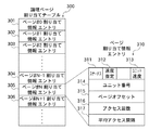
図4は、論理ページ割り当てテーブルの詳細を示す図である。 FIG. 4 is a diagram showing details of the logical page allocation table.
論理ページ割り当てテーブル300は、ストレージデバイス100がホストシステム101に対して提供するストレージサービスにおいて用いられる論理ページの情報を格納するためのテーブルである。この論理ページ割り当てテーブル300は、BLCフラッシュメモリ104上の所定のユニットに保持される。ホストシステム101は、ストレージデバイス100にアクセスする際に、論理ページを指定することによって、BLCフラッシュメモリ104及び/又はMLCフラッシュメモリ105上の所定の物理ページへのアクセスを行う。
The logical page allocation table 300 is a table for storing logical page information used in the storage service provided by the
論理ページ割り当てテーブル300は、ページ#0割り当て情報エントリ301〜ページ#N+1割り当て情報エントリ306、・・・で構成され、それぞれが当該ページの割り当て情報エントリである。ページ割り当て情報エントリ310は、ページ割り当て情報エントリのビットアサインを示している。
The logical page allocation table 300 includes page # 0
ページ割り当て情報エントリ310内のステータス311は、論理ページの物理ページへの割り当て状況を示すビット値であり、“1”で割り当て済み状態、“0”で未割り当て状態を示す。未割り当て状態の論理ページは、初期化後、一度もホストシステム101から書き込みが行われていない状態の論理ページを示すものである。ホストシステム101が未割り当て状態の論理ページに対してデータ読み出しを行った場合は、コントローラ103はRAM106上の読み込みページバッファに0xFFの値でフィルしてホストシステム101に対してデータ渡す。
The
速度指定312は、ユーザが指定することが可能な論理ページの指定速度を示すビット値であり、“0”で速度指定無し、“1”で高速指定を示すものである。ユニット速度313は、当該論理ページが現在割り当てられている物理ページが存在するユニットの速度を示すビット値であり、“0”で低速ユニット、“1”で高速ユニット、を示すものである。本実施の形態では、低速ユニットはMLCフラッシュメモリ105上のユニットを意味し、高速ユニットはBLCフラッシュメモリ104上のユニットを意味する。これにより、任意の物理ページを高速又は低速に割り当てるように指定することができる。速度指定312は、予めユーザが指定することができる。
The
ユニット番号314は、当該論理ページが現在割り当てられている(対応付けられている)物理ページが存在するユニット番号である。ページオフセット315は、当該論理ページが現在割り当てられている物理ページのユニット上のページオフセット番号を示す。アクセス回数316は、当該論理ページへのアクセス回数を示す値が格納されている。平均アクセス間隔317には、当該ページへのアクセス間隔の平均時間が格納されている。アクセス回数316及び平均アクセス間隔317は、後述するページアクセス頻度の判定に用いられる。
The
コントローラ103は、ホストシステム101から指定された論理ページ番号(論理アドレス)を論理ページ割り当てテーブルの内容に基づいてアドレス変換する。そして、この変換アドレスに対応する物理ページ番号(物理アドレス)を使用して、BLCフラッシュメモリ104、MLCフラッシュメモリ105に対するデータの読み出し、書込み及び消去を行う。
The
次に、ホストシステム101とストレージデバイス100との間の通信で用いられるコマンドについて説明する。
Next, commands used for communication between the
図5は、ストレージデバイス100がサポートするコマンドの一覧を示す図である。
FIG. 5 is a diagram showing a list of commands supported by the
ストレージデバイス100は、ホストシステム101からのコマンドとして、「Initialize」、「Page read」、「Page write」、「Set page fast」の4つのコマンドをサポートしている。それぞれのコマンドは0から3個のパラメータを伴って使用される。
The
「Initialize」コマンドは、コマンド番号0x00で指定されるコマンドである。この「Initialize」コマンドは、図示のようにパラメータ無しで用いられ、ストレージデバイスの全領域を初期状態に設定するために用いられる。 The “Initialize” command is a command specified by the command number 0x00. This “Initialize” command is used without parameters as shown in the figure, and is used to set the entire area of the storage device to the initial state.
「Page read」コマンドは、コマンド番号0x10で指定されるコマンドである。この「Page read」コマンドは、指定した論理ページのデータを読み出すために用いられる。「Page read」コマンドは、第一パラメータに読み出し開始位置を指定する開始論理ページ番号が、第二パラメータに読み出しページ数がそれぞれ指定される。ホストシステム101は、「Page read」コマンド及びパラメータを送信後、ストレージデバイス100から所定の読み出しデータを受信する。
The “Page read” command is a command specified by the command number 0x10. This “Page read” command is used to read data of a specified logical page. In the “Page read” command, the start logical page number for specifying the read start position is specified as the first parameter, and the number of read pages is specified as the second parameter. The
「Page write」コマンドは、コマンド番号0x20で指定されるコマンドである。この「Page write」コマンドは、指定した論理ページのデータを書き込むために用いられる。「Page write」コマンドは、第一パラメータに書き込み開始位置を指定する開始論理ページ番号が、第二パラメータに書き込みページ数がそれぞれ指定される。ホストシステム101は、「Page write」コマンド及びパラメータを送信後、ストレージデバイス100に対して所定の書き込みデータを送信する。
The “Page write” command is a command specified by the command number 0x20. This “Page write” command is used to write data of a specified logical page. In the “Page write” command, the start logical page number for specifying the write start position is specified as the first parameter, and the number of write pages is specified as the second parameter. After transmitting the “Page write” command and parameters, the
「Page rate」コマンドは、コマンド番号0x40で指定されるコマンドである。この「Page rate」コマンドは、指定した論理ページのアクセス速度を指定するために用いられる。「Page rate」コマンドは、第一パラメータにアクセス速度を指定する開始論理ページ番号が、第二パラメータにアクセス速度を指定するページ数が、第三パラメータにアクセス速度がそれぞれ指定される。第三パラメータのアクセス速度は“1”が高速、“0”が通常を意味する。 The “Page rate” command is a command specified by the command number 0x40. This “Page rate” command is used to designate the access speed of the designated logical page. In the “Page rate” command, the start logical page number that specifies the access speed is specified as the first parameter, the number of pages that specify the access speed is specified as the second parameter, and the access speed is specified as the third parameter. As for the access speed of the third parameter, “1” means high speed and “0” means normal.
次に、ストレージデバイス100の初期化処理について説明する。
Next, the initialization process of the
ストレージデバイス100は使用される際に、まず初期化処理を行う。通常、初期化処理はストレージデバイスを製造する工場で出荷前に行われるものである。
When the
ホストシステム101は、図5に示した「Initialize」コマンドをストレージデバイス100に対して送信する。ストレージデバイス100において、コントローラ103は、ホストI/F102を介して「Initialize」コマンドを受信すると初期化処理を開始する。
The
図6は、コントローラ103により実行されるストレージデバイス100の初期化処理の詳細を示すフローチャートである。
FIG. 6 is a flowchart showing details of the initialization process of the
コントローラ103は、BLCフラッシュメモリ104及びMLCフラッシュメモリ105に配置される全ブロック(ユニット)の消去を行う(ステップS401)。次に、コントローラ103は、ユニット管理テーブル200の初期化処理を行う(ステップS402)。そして、コントローラ103は、論理ページ割り当てテーブル300の初期化処理を行い(ステップS403)、本処理を終了する。
The
図6のステップS402におけるユニット管理テーブル200の初期化処理の詳細について図7を用いて説明する。 Details of the initialization process of the unit management table 200 in step S402 in FIG. 6 will be described with reference to FIG.
図7は、図6のステップS402におけるユニット管理テーブル200の初期化処理の詳細を示すフローチャートである。 FIG. 7 is a flowchart showing details of the initialization process of the unit management table 200 in step S402 of FIG.
まず、コントローラ103は、不良ユニットビットマップ221の初期化を行う(ステップS411)。次に、消去済みユニットビットマップ222をすべて“1”にセットしてすべてのユニットを消去済み状態にする(ステップS412)。
First, the
次に、すべてのユニットのユニット管理情報240の初期化を、ステップS414からステップS420までのステップを繰り返すことにより行う。まず、コントローラ103は、有効ページ数241の領域にユニットの総ページ数をセットし(ステップS414)、空きページ数242の領域にユニットの総ページ数をセットする(ステップS415)。
Next, the
次に、コントローラ103は、消去待ちページ数243の領域に“0”をセットし(ステップS416)、次の空きページエントリ244の領域に“0”をセットする(ステップS417)。次に、コントローラ103は、物理ページ割り当てテーブル245の全エントリに0xFFFFFFFFをセットし(ステップS418)、消去回数246の領域に1をセットする(ステップS419)。工場出荷時の始めての消去のであれば1をセットし、それ以後の初期化処理であれば既存の値に1加算した値を格納する。そして、ユニット#0からユニット#X+Yまでのすべてのユニットに対して処理が終了したか否かを判別し(ステップS420)、すべてのユニットに対して処理が終了したときはリターンする。
Next, the
次に、図6のステップS403における論理ページ割り当てテーブルの初期化処理の詳細について図8を用いて説明する。 Next, details of the logical page allocation table initialization process in step S403 of FIG. 6 will be described with reference to FIG.
図8は、図6のステップS403における論理ページ割り当てテーブル300の初期化処理の詳細を示すフローチャートである。 FIG. 8 is a flowchart showing details of the initialization process of the logical page allocation table 300 in step S403 of FIG.
すべての論理ページのページ割り当て情報エントリ310(例えば、ページ#0割り当て情報エントリ301〜ページ#2割り当て情報エントリ303)の初期化を、ステップS432からステップS439までのステップを繰り返すことにより行う。
Initialization of page allocation information entries 310 (for example, page # 0
まず、コントローラ103は、ステータス311のビット値をゼロ(未割り当て状態)にセットする(ステップS432)。次に、速度指定312のビット値を“0”(指定無し)にセットする(ステップS433)。次に、ユニット速度313のビット値を“0”(低速ユニット)にセットする(ステップS434)。次に、ユニット番号314に0xFFFFをセットする(ステップS435)。次に、ページオフセット315に0xFFFFをセットする(ステップS436)。次に、アクセス回数316の値を“0”にセットする(ステップS437)。次に、平均アクセス間隔317の値を“0”sec(0xFFFF)にセットする(ステップS438)。そして、ページ0からのすべてのページに対する処理が終了したか否かを判別し(ステップS439)、すべての論理ページのページ割り当て情報エントリ310に対して処理が行われたときはリターンする。
First, the
次に、ホストシステム101がストレージデバイス100からデータの読み出しを行う場合の処理の流れについて説明する。
Next, a processing flow when the
ホストシステム101は、図5に示した「Page read」コマンドをストレージデバイス100に対して送信する。「Page read」コマンドは、パラメータ「開始論理ページ番号」及び「ページ数」を伴って転送される。
The
ストレージデバイス100において、コントローラ103は、ホストI/F102を介して「Page read」コマンド、「開始論理ページ番号」及び「ページ数」を受信するとデータ読み出し処理を開始する。コントローラ103は、「Page read」コマンドと一緒に受信した「開始論理ページ番号」及び「ページ数」のパラメータを基に、データを読み出す論理ページの指定を行う。
In the
図9は、コントローラ103により実行されるデータ読み出し処理の詳細を示すフローチャートである。
FIG. 9 is a flowchart showing details of the data read process executed by the
「Page read」コマンドの「開始論理ページ番号」から「ページ数」で指定された論理ページすべてに対して、ステップS602からステップS607までの処理が実行される。 The processing from step S602 to step S607 is executed for all the logical pages designated by “number of pages” from “start logical page number” of the “Page read” command.
まず、コントローラ103は、論理ページ割り当てテーブル300から当該ページのページ割り当て情報エントリ310を取得する(ステップS602)。次に、取得したページ割り当て情報エントリ310のステータス311のビット値を判定する(ステップS603)。ステータス311のビット値が“0”であれば当該論理ページは未割り当て状態と判断し、ステップS610へ移行する。一方、ステータス311のビット値が“1”であれば当該論理ページは割り当て済み状態と判断し、ステップS604へ移行する。
First, the
ステップS610では、RAM106上に存在する当該論理ページの読み出しのためのページバッファ領域を0xFFでフィルする。すなわち、割り当てられていない論理ページに対しては、データが書き込まれた実績がないので、フラッシュメモリの消去状態である0xFFの値をすべてのバイトの値として返すものである。
In step S610, the page buffer area for reading the logical page existing on the
ステップS604では、ページ割り当て情報エントリ310からユニット番号314、ページオフセット315の値をそれぞれ取得する(ステップS604)。次に、取得したユニット番号、ページオフセットの位置に相当する物理ページの場所をBLCフラッシュメモリ104若しくはMLCフラッシュメモリ105から特定して、特定した物理ページからページデータを読み出す。読み出されたページデータは当該論理ページの読み出しのための読み出しページバッファに格納される(ステップS605)。読み出しページバッファはRAM106上に確保されている。
In step S604, the
次に、論理ページ割り当てテーブル300上の当該ページデータに対応するページ割り当て情報エントリ310のアクセス回数316の値を1インクリメントすると共に、平均アクセス間隔317の値を更新する(ステップS606)。そして、ステップS602からステップS607までの処理が終了し、指定された論理ページのデータ読み出しがすべて終了するとループを抜ける(ステップS607でYES)。
Next, the
コントローラ103は、ホストI/F102に対してレディフラグをセットして(ステップS608)、本処理を終了する。レディフラグがセットされると、ホストシステム101とホストI/F102との通信が開始され、指定されたページのデータの転送が行われる。
The
次に、ホストシステム101がストレージデバイス100に対してデータの書き込みを行う場合の処理の流れについて説明する。
Next, a processing flow when the
ホストシステム101は、図5に示した「Page write」コマンドをストレージデバイス100に対して送信する。「Page write」コマンドは、パラメータ「開始論理ページ番号」、「ページ数」、及び当該ページの書き込みデータを伴って転送される。
The
ストレージデバイス100において、コントローラ103は、ホストI/F102を介して「Page write」コマンド、「開始論理ページ番号」、及び「ページ数」を受信するとデータ書き込み処理を開始する。ホストI/F102は、コマンド、パラメータに続いて送信される当該ページの書き込みデータを受信すると、RAM106上に存在する当該論理ページの書き込みのためのページバッファ領域に当該書き込みデータを格納する。
In the
図10は、コントローラ103により実行されるデータ書き込み処理の詳細を示すフローチャートである。
FIG. 10 is a flowchart showing details of data write processing executed by the
「Page write」コマンドの「開始論理ページ番号」から「ページ数」で指定された論理ページすべてに対して、ステップS702からステップS704までの処理が実行される。 The processing from step S702 to step S704 is executed for all the logical pages designated by “number of pages” from “start logical page number” of the “Page write” command.
まず、コントローラ103は、当該論理ページの開始論理ページ番号と書き込みデータを引数にしてページ書き込み処理を実行する(ステップS702)。ページ書き込み処理の詳細については後述する。
First, the
ステップS702のページ書き込み処理が終了すると、論理ページ割り当てテーブル300上の当該論理ページに対応するページ割り当て情報エントリ310のアクセス回数316及び平均アクセス間隔317の値をそれぞれ更新する。ステップS702からステップS704までの処理が終了し、指定された論理ページの書き込みがすべて終了するとループを抜ける(ステップS704)。
When the page writing process in step S702 is completed, the
次に、コントローラ103は、ホストI/F102に対してレディフラグをセットして(ステップS705)、ホストシステム101に対して書き込み処理が終了したことを通知する。次に、ステップS702のページ書き込み処理において生成されるGCキューに登録されているすべてのユニットに対して、ステップS707からステップS709までの処理が実行される。
Next, the
まず、当該ユニットのユニット管理情報240を参照して消去待ちページ数243の値を取得し、予め設定されている閾値と比較する(ステップS707)。この結果、消去待ちページ数243が閾値よりも小さい場合は(ステップS707でNO)、後述するガバレッジコレクション処理(ステップS708)をスキップしてステップS709へ移行する。一方、消去待ちページ数243が閾値よりも大きい場合は(ステップS707でYES)、ガバレッジコレクション処理(ステップS708)を実行してステップS709へ移行する。このガバレッジコレクション処理はデータ書き込みを行う毎に実行される。
First, the value of the number of pages waiting for
ステップS707からステップS709までの処理が終了し、GCキューに登録されているすべてのユニットに対して処理が終了するとループを抜ける(ステップS709でYES)。 Processing from step S 707 to step S709 is completed, the processing for all the units that are registered in the GC Queue ends leave the loop (YES in step S709).
次に、図10のステップS702におけるページ書き込み処理の詳細について図11を用いて説明する。 Next, details of the page writing process in step S702 of FIG. 10 will be described with reference to FIG.
図11は、図10のステップS702におけるページ書き込み処理の詳細を示すフローチャートである。 FIG. 11 is a flowchart showing details of the page writing process in step S702 of FIG.
まず、コントローラ103は、当該論理ページの開始論理ページ番号と書き込みデータを引数にして、論理ページ割り当てテーブル300から当該論理ページに対応するページ割り当て情報エントリ310を取得する(ステップS801)。次に、取得したページ割り当て情報エントリ310の情報を元に、書き込み先ページ速度判定処理を行う(ステップS802)。この書き込み先ページ速度判定処理の詳細については後述する。
First, the
ステップS802の書き込み先ページ速度判定処理において、高速が決定されていた場合は(ステップS803でYES)、ステップS804の高速物理ページ割り当て処理へ移行する。一方、書き込み先ページ速度判定処理において低速ページに決定されるか又は指定なしの場合は(ステップS803でNO)、ステップS811の低速物理ページ割り当て処理へ移行する。 If the high speed has been determined in the write destination page speed determination process in step S802 (YES in step S803), the process proceeds to the high speed physical page allocation process in step S804. On the other hand, if it is determined that the low-speed page is determined in the write destination page speed determination process or no designation is made (NO in step S803), the process proceeds to the low-speed physical page allocation process in step S811.
ステップS804の高速物理ページ割り当て処理及びステップS811の低速物理ページ割り当て処理では、それぞれBLCフラッシュメモリ104及びMLCフラッシュメモリ105からページ書き込みのための物理ページが割り当てられる。ステップS804及びステップS811における物理ページ割り当て処理の詳細については後述する。
In the high-speed physical page allocation process in step S804 and the low-speed physical page allocation process in step S811, physical pages for page writing are allocated from the
次に、コントローラ103は、RAM106上の書き込みページバッファにある当該ページの書き込みデータを、アクセス速度が指定された物理ページに書き込む(ステップS805)。次に、論理ページ割り当てテーブル300上の当該ページに対応するページ割り当て情報エントリ310のユニット番号314及びページオフセット315の領域に対して、割り当てた物理ページの位置を指す値を書き込み、論理ページ割り当てテーブルを更新する。
Next, the
次に、コントローラ103は、ページ割り当て情報エントリ310のステータス311のビット値を判定する(ステップS807)。ステータス311のビット値が“0”であれば当該論理ページは未割り当て状態と判断し、ステップS812へ移行する。ステータス311のビット値が“1”であれば当該論理ページは割り当て済み状態と判断し、ステップS808へ移行する。
Next, the
ステップS812では、コントローラ103は、論理ページ割り当てテーブル300上のページ割り当て情報エントリ310のステータス311のビット値を“1”にセットしてリターンする。ステップS808では、以前の書き込みデータ(元データ)が保持されていた物理ページについて、当該ユニットのユニット管理情報240の物理ページ割り当てテーブル245の当該物理ページのエントリを0xFFFFFFF0にセットする。さらに消去待ちページ数243の値を1インクリメント(+1)して消去待ちに変更する。
In step S812, the
次に、コントローラ103は、当該ユニットのユニット番号をGCキューに追加し、ガバレッジコレクションの対象の候補となるユニットとして保管して(ステップS809)、リターンする。
Next, the
次に、図11のステップS802における書き込み先ページ速度判定処理の詳細について図12を用いて説明する。 Next, details of the write destination page speed determination process in step S802 of FIG. 11 will be described with reference to FIG.
図12は、図11のステップS802における書き込み先ページ速度判定処理の詳細を示すフローチャートである。 FIG. 12 is a flowchart showing details of the write destination page speed determination process in step S802 of FIG.
まず、コントローラ103は、データの書き込み先となる論理ページに対応するページ割り当て情報エントリ310を論理ページ割り当てテーブル300から取得する(ステップS821)。
First, the
次に、コントローラ103は、ページ割り当て情報エントリ310上の速度指定312のビット値を判定する(ステップS822)。速度指定312のビット値が“1”であれば予め高速指定がなされていると判断し、書き込み先の論理ページを高速に決定して(ステップS825)、リターンする。一方、速度指定312のビット値が“0”であれば予め高速指定がなされていないか又はなんら指定されていないと判断し、ステップS823に移行する。
Next, the
ステップS823では、コントローラ103は、ページ割り当て情報エントリ310上のアクセス回数316の値を判定する。アクセス回数316の値が所定値よりも大きい場合は(ステップS823でYES)、ステップS824に移行する。一方、アクセス回数316の値が所定値よりも小さい場合は(ステップS823でNO)、書き込み先の論理ページを低速に決定して(ステップS826)、リターンする。
In step S823, the
ステップS824では、コントローラ103は、ページ割り当て情報エントリ310上の平均アクセス間隔317の値を評価する。平均アクセス間隔317の値が所定値よりも小さい場合は(ステップS824でYES)、ステップS825に移行する。一方、平均アクセス間隔317の値が所定値よりも大きい場合は(ステップS824でNO)、ステップS826に移行する。
In step S824, the
本処理により、図13に示す条件で物理ページが高速領域に割り当てられることとなる。すなわち、速度指定が高速でなくともアクセス回数が多く且つ平均アクセス間隔が小さい場合、データの書き込み先を高速ページ(BLCフラッシュメモリ)に決定するので、頻繁にアクセスされるページをアクセス頻度に応じて高速領域に割り振ることができる。 With this processing, the physical page is allocated to the high-speed area under the conditions shown in FIG. That is, even if the speed designation is not high speed, if the number of accesses is large and the average access interval is small, the data write destination is determined to be a high speed page (BLC flash memory). Can be allocated to a high speed region.
次に、図11のステップS804及びステップS811における物理ページ割り当て処理の詳細について図14を用いて説明する。 Next, details of the physical page allocation processing in steps S804 and S811 in FIG. 11 will be described with reference to FIG.
図14は、物理ページ割り当て処理の詳細を示すフローチャートである。 FIG. 14 is a flowchart showing details of physical page allocation processing.
まず、コントローラ103は、ユニット管理テーブル200上のユニット管理情報240に対して検索を行い、空きページのあるユニットを見つける(ステップS841)。ここで、割り当てたい物理ページが高速ページである場合は、ユニット#0からユニット#X−1までのユニット管理情報240を検索対象とする。割り当てたい物理ページが低速ページ(MLCフラッシュメモリ)である場合は、ユニット#Xからユニット#X+Yまでのユニット管理情報240を検索対象とする。空きページのあるユニットが見つかったときは、当該ユニットのユニット管理情報240上の空きページ数242の値から1デクリメント(−1)する(ステップS842)。
First, the
次に、コントローラ103は、当該ユニットのユニット管理情報240上の次の空きページエントリ244の値を戻り値にセットし(ステップS843)、次の空きページエントリ244の値に1インクリメント(+1)する(ステップS844)。そして、当該ユニットの物理ページ割り当てテーブル245上の割り当て物理ページに、該当する物理ページのエントリに割り当てる論理ページの番号をセットして(ステップS845)、リターンする。本処理により、コントローラ103は、戻り値として割り当てページエントリを返す。
Next, the
次に、図10のステップS708におけるガバレッジコレクション処理の詳細について図15を用いて説明する。 Next, details of the garbage collection process in step S708 of FIG. 10 will be described with reference to FIG.
図15は、図10のステップS708におけるガバレッジコレクション処理の詳細を示すフローチャートである。当該ユニットの物理ページすべてに対して、ステップS902からステップS907までの処理が実行される。 FIG. 15 is a flowchart showing details of the garbage collection process in step S708 of FIG. The processing from step S902 to step S907 is executed for all physical pages of the unit.
まず、コントローラ103は、物理ページ割り当てテーブル245からループ毎に順に物理ページのエントリを取得する(ステップS902)。取得したエントリが0xFFFFFFFFであるときは、当該ページは空きページであるとみなして(ステップS903でYES)、ステップS904〜S906をスキップしてループを継続する。一方、取得したエントリが0xFFFFFFF0であるときは、当該ページは消去待ちページであるとみなして(ステップS904でYES)、ステップS905,S906をスキップしてループを継続する。
First, the
ステップS905では、コントローラ103は、当該物理ページに書き込まれているページデータをRAM106上の読み出しページバッファに読み出す。次に、読み出したページデータを別の物理ページに移すためにページ書き込み処理を実行する(ステップS906)。このページ書き込み処理は、上述した図11に示した処理と同様の処理である。
In step S <b> 905, the
なお、読み出したページデータを別の物理ページに移す場合、移動後の物理ページに割り当てられた論理ページのアクセス速度を移動前の速度に指定にするかまたは移動後の物理ページに割り当てられた論理ページのアクセス速度をアクセス頻度に応じて指定する。また、論理ページに対応する書き込みデータを移動後の物理ページに書き込むと共に、論理ページ割り当てテーブル300を更新する。 When moving the read page data to another physical page, specify the access speed of the logical page assigned to the physical page after movement as the speed before movement, or the logical page assigned to the physical page after movement. Specify the page access speed according to the access frequency. In addition, write data corresponding to the logical page is written to the physical page after movement, and the logical page allocation table 300 is updated.
物理ページ割り当てテーブル245のすべてのエントリに対して、ステップS902からステップS907までの処理が終了するとループを抜ける(ステップS907でYES)。 When the processing from step S902 to step S907 is completed for all entries in the physical page allocation table 245, the process exits the loop (YES in step S907).
ステップS908では、コントローラ103は、すべての物理ページへの処理が終わると当該ユニット上には有効なデータは残っていない状態になるので、ユニット物理消去を行う。ユニット物理消去は、BLCフラッシュメモリ104若しくはMLCフラッシュメモリ105の当該消去ブロックを物理的に消去する。次に、ユニット論理消去処理を行う(ステップS909)。ユニット論理消去処理の詳細については後述する。
In step S908, the
次に、図15のステップS909におけるユニット論理消去処理の詳細について図16を用いて説明する。 Next, details of the unit logical erasure process in step S909 of FIG. 15 will be described with reference to FIG.
図16は、図15のステップS909におけるユニット論理消去処理の詳細を示すフローチャートである。 FIG. 16 is a flowchart showing details of the unit logical erasure process in step S909 of FIG.
まず、コントローラ103は、ユニット管理テーブル200の消去済みユニットビットマップ222上の当該ユニットのビット値を“1”にセットする(ステップS951)。次に、当該ユニットのユニット管理情報240上の有効ページ数241にユニットの総ページ数であるMをセットする(ステップS952)。次に、当該ユニットのユニット管理情報240上の空きページ数242にユニットの総ページ数であるMをセットする(ステップS953)。
First, the
次に、コントローラ103は、当該ユニットのユニット管理情報240上の消去待ちページ数243に“0”をセットする(ステップS954)。次に、当該ユニットのユニット管理情報240上の次の空きページエントリ244に“0”をセットする(ステップS955)。次に、当該ユニットのユニット管理情報240上の物理ページ割り当てテーブル245のすべてのエントリに0xFFFFFFFFFをセットする。さらに、当該ユニットのユニット管理情報240上の消去回数246の値を1インクリメント(+1)する。これにより、当該ユニットのユニット管理情報240が消去状態となる。
Next, the
次に、ホストシステム101からストレージデバイス100に対して論理ページへのアクセス速度を指定する処理の流れについて説明する。
Next, the flow of processing for designating the access speed to the logical page from the
ホストシステム101は、図5に示した「Page rate」コマンドをストレージデバイス100に対して送信する。「Page rate」コマンドはパラメータ「開始論理ページ番号」、「ページ数」、及び「アクセス速度」を伴って転送される。ストレージデバイス100において、コントローラ103は、ホストI/F102を介して「Page rate」コマンド、「開始論理ページ番号」、「ページ数」、及び「速度」のパラメータを受信すると、論理ページへのアクセス速度の指定処理を開始する。
The
図17は、コントローラ103により実行されるページのアクセス速度指定処理の詳細を表したフローチャートである。
FIG. 17 is a flowchart showing details of a page access speed designation process executed by the
コントローラ103は、「Page rate」コマンドと一緒に受信した「開始論理ページ番号」及び「ページ数」のパラメータを基に、アクセス速度を指定する論理ページの指定を行う。指定された論理ページすべてに対して、ステップS1002からステップS1004までの処理が実行される。
The
まず、コントローラ103は論理ページ割り当てテーブル300より当該ページのページ割り当て情報エントリ310を取得する(ステップS1002)。次に、当該ページのページ割り当て情報エントリ310のユニット速度313のビット値にパラメータ「アクセス速度」の値をセットする(ステップS1003)。
First, the
ステップS1002からステップS1004までの処理を繰り返すことにより、指定された論理ページの速度指定がすべて終了するとループを抜ける(ステップS1004でYES)。次に、コントローラ103は、ホストI/F102に対してレディフラグをセットする(ステップS1005)。レディフラグがセットされると、ホストシステム101とホストI/F102の通信が開始され、アクセス速度指定が終了したことをホストシステム101に通知する。
By repeating the processing from step S1002 to step S1004, when all the speed designations of the designated logical page are completed, the loop is exited (YES in step S1004). Next, the
予めアクセス速度が指定されている場合は、本処理により、データ書き込み時に、指定されたアクセス速度が物理ページに割り当てられる。また、アクセス状況に応じて、上書き又はガバレッジコレクション処理が発生して論理ページの割り当てられている物理ページの位置が変更になるときに、速度判定に応じた物理ページに割り当てられる。 When the access speed is designated in advance, the designated access speed is assigned to the physical page at the time of data writing by this processing. Further, when the position of a physical page to which a logical page is allocated is changed due to an overwrite or a garbage collection process depending on the access status, the logical page is allocated to a physical page according to speed determination.
次に、ホストシステム101上で動作するファイルシステムがストレージデバイス100を論理フォーマットするときの処理について説明する。
Next, processing when the file system operating on the
図18は、ホストシステム101上で動作するファイルシステムのフォーマット処理を示すフローチャートである。図19は、FATファイルシステムでフォーマットされているブロックデバイスの内部のデータ構造を示す図である。
FIG. 18 is a flowchart showing the format processing of the file system operating on the
ホストシステム101は、MBR1101〜ルートディレクトリエントリ1106の配置されるべきセクタの論理ページを「Page rate」コマンドを用いて高速ページに指定する(ステップS1201〜ステップS1204)。
The
次に、ホストシステム101は、MBR1101〜ルートディレクトリエントリ1106の値を「Page write」コマンドを用いて書き換えることによって、FATファイルシステムの初期状態にする(ステップS1205〜ステップS1208)。そして、ファイルシステムのフォーマット処理を終了する。この「Page write」コマンドが実行されることにより、ステップS1201〜ステップS1204において指定された論理ページはすべて高速ページとしてBLCフラッシュメモリ104上の物理ページへ配置される。すなわち、フォーマットが実行されると、ファイルシステムで用いられる管理領域のMBR1101〜ルートディレクトリエントリ(RootDir)1106といった、頻繁にアクセスされる可能性の高い記憶領域が高速ページに配置されることとなる。
Next, the
FATファイルシステムにおいて、ファイルやディレクトリを生成する場合には、ルートディレクトリエントリ1106又は不図示のサブディレクトリ領域にディレクトリエントリを生成して配置する必要がある。したがって、ルートディレクトリエントリ1106以外にも、サブディレクトリを作成してファイルを配置させる場合、論理ページを予め「Page rate」コマンドを用いて高速ページに指定することが可能である。この論理ページは、サブディレクトリ領域として使用するクラスタ位置に相当する。これにより、随時生成されるサブディレクトリ領域も、高速ページに配置することが可能となる。
When a file or directory is generated in the FAT file system, it is necessary to generate and place a directory entry in the
このようにして、ルートディレクトリエントリ及びサブディレクトリエントリが高速ページに配置されることによって、FATファイルシステムにおけるディレクトリエントリのパースの処理が高速になる。そして、ファイル名の検索や新規生成ファイルの名前重複検査処理が高速になり、ファイルアクセスの相対的な高速化を実現することができる。 In this way, the root directory entry and the subdirectory entry are arranged in the high-speed page, so that the parsing process of the directory entry in the FAT file system is accelerated. Further, the search for the file name and the name duplication check process for the newly generated file are accelerated, and the relative speeding up of the file access can be realized.
上記第1の実施の形態によれば、アクセス速度の異なる記憶手段(又は記憶領域)を有するストレージデバイスにアクセスする際に、データを書き込む記憶領域が限定されることなく、任意のデータをアクセス速度が高速な記憶手段等に割り振ることが可能となる。また、記憶領域に対するアクセス頻度を記録し、頻繁にアクセスされる記憶領域を高速な記憶領域に割り振ることができ、アクセス頻度の高いデータやファイルのアクセスを効果的に高速化することが可能となる。 According to the first embodiment, when accessing a storage device having storage means (or storage areas) having different access speeds, any data can be accessed at any access speed without being limited to a storage area to which data is written. Can be allocated to high-speed storage means. In addition, the access frequency to the storage area can be recorded, and the frequently accessed storage area can be allocated to a high-speed storage area, so that access to frequently accessed data and files can be effectively speeded up. .
また、データの上書きやガバレッジコレクション処理等によって論理ページ(論理ブロック)と物理ページ(物理ブロック)の割り当てが変更になった場合においても、所望のアクセス速度を有する記憶領域にファイルやデータの配置を維持することが可能となる。 In addition, even when the allocation of logical pages (logical blocks) and physical pages (physical blocks) is changed due to data overwriting or garbage collection processing, files and data are placed in a storage area with the desired access speed. Can be maintained.
次に、本発明の第2の実施形態について説明する。 Next, a second embodiment of the present invention will be described.
本発明の第2の実施の形態に係るメモリ管理装置は、その構成(図1〜図5)が上記第1の実施の形態に係るメモリ管理装置と同じであり、第1の実施の形態と同様の部分については、同一の符号を用いてその説明を省略する。以下に、上記第1の実施の形態と異なる点のみを説明する。 The memory management device according to the second embodiment of the present invention has the same configuration (FIGS. 1 to 5) as that of the memory management device according to the first embodiment. About the same part, the description is abbreviate | omitted using the same code | symbol. Only differences from the first embodiment will be described below.
上述した第1の実施形態では、図10に示すように、ストレージデバイス100がデータ書き込み処理を行うタイミングでガバレッジコレクション処理を行った。本第2の実施形態では、ガバレッジコレクション処理をデータ書き込み時毎に行わず、バックグラウンド処理として非同期に行うものである。これにより、書き込み時の処理を軽減することが可能となり、相対的に書き込み時の処理時間が短くなる。
In the first embodiment described above, as shown in FIG. 10, the garbage collection process is performed at the timing when the
第2の実施形態における、ホストシステム101からストレージデバイス100に対してデータの書き込みを行う場合の処理の流れについて説明する。
A flow of processing when data is written from the
ホストシステム101は、図5に示した「Page write」コマンドをストレージデバイス100に対して送信する。「Page write」コマンドは、パラメータ「開始論理ページ番号」、「ページ数」、及び当該ページの書き込みデータを伴って転送される。
The
ストレージデバイス100において、コントローラ103は、ホストI/F102を介して「Page write」コマンド、「開始論理ページ番号」、及び「ページ数」を受信するとデータ書き込み処理を開始する。ホストI/F102は、コマンド、パラメータに続いて送信される当該ページの書き込みデータを受信すると、RAM106上に存在する当該論理ページの書き込みのためのページバッファ領域に当該書き込みデータを格納する。
In the
図20は、本発明の第2の実施形態におけるストレージデバイス100のコントローラ103により実行されるデータの書き込み処理の詳細を示すフローチャートである。なお、図20のステップS702からステップS705までの処理は、図10のステップS702からステップS705までの処理と同じであるため、その説明を省略する。
FIG. 20 is a flowchart showing details of data write processing executed by the
次に、バックグラウンドで実行されるガバレッジコレクション(GC)処理について説明する。 Next, a garbage collection (GC) process executed in the background will be described.
図21は、コントローラ103によりバックグラウンドで実行されるガバレッジコレクション処理の詳細を示すフローチャートである。図21のステップS707からステップS709までの処理は、図10のステップS707からステップS709までの処理と同じであるため、その説明を省略する。
FIG. 21 is a flowchart showing details of the garbage collection process executed by the
図21に示すガバレッジコレクション処理は、所定の時間間隔毎に、定期的に行われるものである。なお、このガバレッジコレクション処理は、定期的に実行する代わりに、ストレージデバイス100へのアクセスが所定回数実施される毎に行ってもよい。
The garbage collection process shown in FIG. 21 is periodically performed at predetermined time intervals. Note that this garbage collection processing may be performed every time access to the
次に、本発明の第3の実施形態について説明する。 Next, a third embodiment of the present invention will be described.
本発明の第3の実施の形態に係るメモリ管理装置は、その構成(図1〜図5)が上記第1の実施の形態に係るメモリ管理装置と同じであり、第1の実施の形態と同様の部分については、同一の符号を用いてその説明を省略する。以下に、上記第1の実施の形態と異なる点のみを説明する。 The memory management device according to the third embodiment of the present invention has the same configuration (FIGS. 1 to 5) as that of the memory management device according to the first embodiment. About the same part, the description is abbreviate | omitted using the same code | symbol. Only differences from the first embodiment will be described below.
上述した第1の実施形態では、図17に示すように、ホストシステム101が「Page rate」コマンドでページ速度を指定した場合に、当該ページのページ割り当て情報エントリ310の速度指定312のビット値を変更するのみであった。
In the first embodiment described above, as shown in FIG. 17, when the
本第3の実施形態では、「Page rate」コマンドでページ速度を指定した場合に、当該ページのページ割り当て情報エントリ310の速度指定312のビット値を変更する。それと共に、当該ページに既に有効データが書き込まれていたときは、そのデータを指定された高速ページに移動する処理を行う。これにより、「Page rate」コマンドを書き込み済みのページに対して指定した場合においても、指定した高速ページに随時割り当てを変更することが可能となる。
In the third embodiment, when the page rate is designated by the “Page rate” command, the bit value of the
本第3の実施形態における、ホストシステム101からストレージデバイス100に対して論理ページの速度を指定する処理の流れについて説明する。
A flow of processing for designating a logical page speed from the
ホストシステム101は、図5に示した「Page rate」コマンドをストレージデバイス100に対して送信する。「Page rate」コマンドは、パラメータ「開始論理ページ番号」、「ページ数」、及び「速度」を伴って転送される。コントローラ103は、ホストI/F102を介して「Page rate」コマンド、「開始論理ページ番号」、「ページ数」、及び「アクセス速度」のパラメータを受信する。そうすると、論理ページへのアクセス速度の指定処理を開始する。
The
図22は、本発明の第3の実施形態におけるストレージデバイス100のコントローラ103により実行されるページ速度指定処理の詳細を示すフローチャートである。
FIG. 22 is a flowchart showing details of a page speed designation process executed by the
コントローラ103は、「Page read」コマンドと一緒に受信した「開始論理ページ番号」及び「ページ数」のパラメータを基に、アクセス速度を指定する論理ページの指定を行う。指定された論理ページすべてに対して、ステップS1002,S1501〜S1504,S1003,S1004のステップが実行される。なお、ステップS1501〜ステップS1505を除く処理は、上述した図17に示した処理と同じであるため、その説明を省略する。
The
ステップS1501では、コントローラ103は、当該ページのページ割り当て情報エントリ310のステータス311のビット値が“0”であれば、当該ページは空きページであるとみなしてステップS1003へ移行する。ステップS1502では、当該ページのページ割り当て情報エントリ310のユニット速度313が「Page rate」コマンドで指定された速度と同じであれば、ステップS1003へ移行する。
In step S1501, if the bit value of the
ステップS1503では、当該ページに既に書き込まれてあるページデータをRAM106上のページバッファに読み出す。次に、読み出したページデータを別の物理ページに移すためにページ書き込み処理を実行する(ステップS1504)。このページ書き込み処理は、図11に示した処理と同じである。 In step S1503, the page data already written on the page is read into the page buffer on the RAM. Next, page write processing is executed to move the read page data to another physical page (step S1504). This page writing process is the same as the process shown in FIG.
上記実施の形態においては、図9のステップ606及び図10のステップ703において論理ページ割り当てテーブル300上のページ割り当て情報エントリ310のアクセス回数316及び平均アクセス間隔317の値の更新を行った。しかしながら、ストレージデバイス100の用途によっては、データ書き込み処理においてのみ若しくはデータ読み出し処理においてのみ、アクセス回数316及び平均アクセス間隔317の値の更新を行うようにしてもよい。
In the above embodiment, the values of the
データ書き込み処理においてのみアクセス回数316及び平均アクセス間隔317の値の更新を行うようにすれば、頻繁に書き込みを行うページについて高速領域に配置されるという効果を奏する。また、データ読み出し処理においてのみアクセス回数316及び平均アクセス間隔317の値の更新を行うようにすれば、頻繁に読み出しを行うページについて高速領域に配置されるという効果を奏する。
If the values of the
上記各実施形態においては、MLCフラッシュメモリ及びBLCフラッシュメモリを用いてストレージデバイスを構成したが、この限りではない。例えば、HDDを用いて第二のメモリ領域を構成してもよい。 In each of the above embodiments, the storage device is configured using the MLC flash memory and the BLC flash memory, but this is not restrictive. For example, the second memory area may be configured using an HDD.
また、本発明の目的は、以下の処理を実行することによって達成される。即ち、上述した実施形態の機能を実現するソフトウェアのプログラムコードを記録した記憶媒体を、システム或いは装置に供給し、そのシステム或いは装置のコンピュータ(またはCPUやMPU等)が記憶媒体に格納されたプログラムコードを読み出す処理である。この場合、記憶媒体から読み出されたプログラムコード自体が前述した実施の形態の機能を実現することになり、そのプログラムコード及び該プログラムコードを記憶した記憶媒体は本発明を構成することになる。 The object of the present invention is achieved by executing the following processing. That is, a storage medium that records a program code of software that realizes the functions of the above-described embodiments is supplied to a system or apparatus, and a computer (or CPU, MPU, etc.) of the system or apparatus is stored in the storage medium. This is the process of reading the code. In this case, the program code itself read from the storage medium realizes the functions of the above-described embodiments, and the program code and the storage medium storing the program code constitute the present invention.
また、プログラムコードを供給するための記憶媒体としては、次のものを用いることができる。例えば、フロッピー(登録商標)ディスク、ハードディスク、光磁気ディスク、CD−ROM、CD−R、CD−RW、DVD−ROM、DVD−RAM、DVD−RW、DVD+RW、磁気テープ、不揮発性のメモリカード、ROM等である。または、プログラムコードをネットワークを介してダウンロードしてもよい。 Moreover, the following can be used as a storage medium for supplying the program code. For example, floppy (registered trademark) disk, hard disk, magneto-optical disk, CD-ROM, CD-R, CD-RW, DVD-ROM, DVD-RAM, DVD-RW, DVD + RW, magnetic tape, nonvolatile memory card, ROM or the like. Alternatively, the program code may be downloaded via a network.
また、コンピュータが読み出したプログラムコードを実行することにより、上記実施の形態の機能が実現される場合も本発明に含まれる。加えて、そのプログラムコードの指示に基づき、コンピュータ上で稼動しているOS(オペレーティングシステム)等が実際の処理の一部または全部を行い、その処理によって前述した実施形態の機能が実現される場合も含まれる。 Further, the present invention includes a case where the function of the above-described embodiment is realized by executing the program code read by the computer. In addition, an OS (operating system) running on the computer performs part or all of the actual processing based on an instruction of the program code, and the functions of the above-described embodiments are realized by the processing. Is also included.
更に、前述した実施形態の機能が以下の処理によって実現される場合も本発明に含まれる。即ち、記憶媒体から読み出されたプログラムコードが、コンピュータに挿入された機能拡張ボードやコンピュータに接続された機能拡張ユニットに備わるメモリに書き込まれる。その後、そのプログラムコードの指示に基づき、その機能拡張ボードや機能拡張ユニットに備わるCPU等が実際の処理の一部または全部を行う場合である。 Furthermore, a case where the functions of the above-described embodiment are realized by the following processing is also included in the present invention. That is, the program code read from the storage medium is written in a memory provided in a function expansion board inserted into the computer or a function expansion unit connected to the computer. Thereafter, based on the instruction of the program code, the CPU or the like provided in the function expansion board or function expansion unit performs part or all of the actual processing.
また、コンピュータが読み出したプログラムコードを実行することにより、前述した各実施の形態の機能が実現される場合も本発明に含まれる。加えて、そのプログラムコードの指示に基づき、コンピュータ上で稼働しているOSなどが実際の処理の一部または全部を行い、その処理によって前述した実施の形態の機能が実現する場合も含まれる。この場合、上記プログラムは、該プログラムを記憶した記憶媒体から直接、又はインターネット、商用ネットワーク、若しくはローカルエリアネットワーク等に接続された不図示の他のコンピュータやデータベース等からダウンロードすることにより供給される。 Further, the present invention includes a case where the functions of the above-described embodiments are realized by executing the program code read by the computer. In addition, there is a case where the OS running on the computer performs part or all of the actual processing based on the instruction of the program code, and the functions of the above-described embodiments are realized by the processing. In this case, the program is supplied by downloading directly from a storage medium storing the program or from another computer or database (not shown) connected to the Internet, a commercial network, a local area network, or the like.
100 ストレージデバイス
101 ホストシステム
102 ホストI/F
103 コントローラ
104 BLC(Binary Level Cell:2値型)フラッシュメモリ
105 MLC(Multi-Level Cell:多値型)フラッシュメモリ
106 RAM
100
103
Claims (20)
前記第1の記憶部よりも高速にアクセス可能な第2の記憶部と、
論理アドレスのアクセス速度に関する速度情報をホスト装置から受け取る受信手段と、
前記受信手段により受け取った前記速度情報に基づいて、前記論理アドレスに対して前記第1の記憶部の物理アドレスまたは前記第2の記憶部の物理アドレスを割り当て、論理アドレスの情報を含む書き込み指示を前記受信手段が前記ホスト装置から受け取った場合、前記受信手段が受け取った前記書き込み指示に含まれる論理アドレスに対して割り当てられた物理アドレスに対して書き込みを行う制御手段とを備えることを特徴とする記憶装置。 A first storage unit;
A second storage unit accessible at a higher speed than the first storage unit;
Receiving means for receiving speed information on the access speed of the logical address from the host device;
Based on the speed information received by the receiving means, a physical address of the first storage unit or a physical address of the second storage unit is assigned to the logical address, and a write instruction including logical address information is issued. Control means for writing to a physical address assigned to a logical address included in the write instruction received by the reception means when the reception means is received from the host device. Storage device.
第1の記憶部と、
前記第1の記憶部よりも高速にアクセス可能な第2の記憶部と、
論理アドレスのアクセス速度に関する速度情報を前記ホスト装置から受け取る受信手段と、
前記受信手段により受け取った前記速度情報に基づいて、前記論理アドレスに対して前記第1の記憶部の物理アドレスまたは前記第2の記憶部の物理アドレスを割り当て、論理アドレスの情報を含む書き込み指示を前記受信手段が前記ホスト装置から受け取った場合、前記受信手段が受け取った前記書き込み指示に含まれる論理アドレスに対して割り当てられた前記第1の記憶部の物理アドレスまたは前記第2の記憶部の物理アドレスに対して書き込みを行う制御手段とを有することを特徴とするメモリ管理システム。 A host device;
A first storage unit;
A second storage unit accessible at a higher speed than the first storage unit;
Receiving means for receiving speed information on the access speed of the logical address from the host device;
Based on the speed information received by the receiving means, a physical address of the first storage unit or a physical address of the second storage unit is assigned to the logical address, and a write instruction including logical address information is issued. When the receiving unit receives from the host device, the physical address of the first storage unit assigned to the logical address included in the write instruction received by the receiving unit or the physical unit of the second storage unit A memory management system comprising: control means for writing to an address.
前記ホスト装置は、アクセス先の論理アドレスを指定し、前記指定した論理アドレスのアクセス速度に関する速度指定コマンドと、前記指定した論理アドレスに対する書き込みコマンドまたは読み出しコマンドを前記記憶装置に出力すると共に、前記記憶装置の初期化時に、ファイルアロケーションテーブルとルートディレクトリエントリを書き込むための論理アドレスを指定し、前記ファイルアロケーションテーブルとルートディレクトリエントリを書き込むための論理アドレスが高速アクセスであることを示す前記速度指定コマンドを前記記憶装置に出力し、
前記記憶装置は、前記速度指定コマンドに基づいて、前記速度指定コマンドにより指定された論理アドレスに対して前記第1の記憶部または第2の記憶部の物理アドレスを割り当て、前記書き込みまたは読み出しコマンドにより指定された論理アドレスに対して割り当てられた物理アドレスにアクセスすると共に、前記初期化時に前記ホスト装置から出力された前記速度指定コマンドに基づいて、前記ファイルアロケーションテーブルとルートディレクトリエントリを書き込むための論理アドレスに対して前記第2の記憶部の物理アドレスを割り当てることを特徴とするメモリ管理システム。 A memory management system comprising: a storage device having a first storage unit and a second storage unit that can be accessed faster than the first storage unit; and a host device that accesses the storage device according to a FAT file system. There,
The host device designates a logical address of an access destination, outputs a speed designation command relating to an access speed of the designated logical address, a write command or a read command for the designated logical address to the storage device, and stores the storage A logical address for writing a file allocation table and a root directory entry is designated at the time of initialization of the device, and the speed designation command indicating that the logical address for writing the file allocation table and the root directory entry is high-speed access. Output to the storage device,
The storage device allocates a physical address of the first storage unit or the second storage unit to a logical address specified by the speed specification command based on the speed specification command, and by the write or read command A logic for accessing the physical address assigned to the designated logical address and writing the file allocation table and root directory entry based on the speed designation command output from the host device at the time of initialization. A memory management system, wherein a physical address of the second storage unit is assigned to an address.
前記記憶装置は、前記ホスト装置から出力された前記速度指定コマンドに基づいて、前記サブディレクトリエントリを書き込むための論理アドレスに対して前記第2の記憶部の物理アドレスを割り当てることを特徴とする請求項11に記載のメモリ管理システム。 The host device designates a logical address for writing a subdirectory entry, and outputs the speed designation command indicating that the logical address for writing the subdirectory entry is high-speed access to the storage device;
The storage device assigns a physical address of the second storage unit to a logical address for writing the subdirectory entry based on the speed designation command output from the host device. Item 12. The memory management system according to Item 11.
前記受信手段により受け取った前記速度情報に基づいて、前記論理アドレスに対して前記第1の記憶部の物理アドレスまたは前記第2の記憶部の物理アドレスを割り当て、論理アドレスの情報を含む書き込み指示を前記受信手段が前記ホスト装置から受け取った場合、前記受信手段が受け取った前記書き込み指示に含まれる論理アドレスに対して割り当てられた前記第1の記憶部の物理アドレスまたは前記第2の記憶部の物理アドレスに対して書き込みを行うことを特徴とする記憶装置の制御方法。 A storage device control method comprising: a first storage unit; a second storage unit that can be accessed at a higher speed than the first storage unit; and a receiving unit that receives speed information related to an access speed of a logical address from a host device. Because
Based on the speed information received by the receiving means, a physical address of the first storage unit or a physical address of the second storage unit is assigned to the logical address, and a write instruction including logical address information is issued. When the receiving unit receives from the host device, the physical address of the first storage unit assigned to the logical address included in the write instruction received by the receiving unit or the physical unit of the second storage unit A method for controlling a storage device, wherein writing to an address is performed.
Priority Applications (3)
| Application Number | Priority Date | Filing Date | Title |
|---|---|---|---|
| JP2007077553A JP5224706B2 (en) | 2007-03-23 | 2007-03-23 | Storage device and storage device control method |
| US12/047,560 US8335893B2 (en) | 2007-03-23 | 2008-03-13 | Storage device, system, and method that determines a physical address of a memory unit allocated to a logical address or allocates a logical address to a physical address of a memory unit, based on access speed information of the logical address |
| KR1020080026128A KR100975825B1 (en) | 2007-03-23 | 2008-03-21 | Memory device, Memory system, and Memory method |
Applications Claiming Priority (1)
| Application Number | Priority Date | Filing Date | Title |
|---|---|---|---|
| JP2007077553A JP5224706B2 (en) | 2007-03-23 | 2007-03-23 | Storage device and storage device control method |
Publications (3)
| Publication Number | Publication Date |
|---|---|
| JP2008242503A JP2008242503A (en) | 2008-10-09 |
| JP2008242503A5 JP2008242503A5 (en) | 2010-05-06 |
| JP5224706B2 true JP5224706B2 (en) | 2013-07-03 |
Family
ID=39775886
Family Applications (1)
| Application Number | Title | Priority Date | Filing Date |
|---|---|---|---|
| JP2007077553A Expired - Fee Related JP5224706B2 (en) | 2007-03-23 | 2007-03-23 | Storage device and storage device control method |
Country Status (3)
| Country | Link |
|---|---|
| US (1) | US8335893B2 (en) |
| JP (1) | JP5224706B2 (en) |
| KR (1) | KR100975825B1 (en) |
Families Citing this family (37)
| Publication number | Priority date | Publication date | Assignee | Title |
|---|---|---|---|---|
| JP2008090876A (en) * | 2006-09-29 | 2008-04-17 | Toshiba Corp | Nonvolatile semiconductor memory device |
| US20100169708A1 (en) * | 2008-12-29 | 2010-07-01 | John Rudelic | Method and apparatus to profile ram memory objects for displacment with nonvolatile memory |
| US20100287217A1 (en) * | 2009-04-08 | 2010-11-11 | Google Inc. | Host control of background garbage collection in a data storage device |
| US8566508B2 (en) | 2009-04-08 | 2013-10-22 | Google Inc. | RAID configuration in a flash memory data storage device |
| US8433845B2 (en) | 2009-04-08 | 2013-04-30 | Google Inc. | Data storage device which serializes memory device ready/busy signals |
| WO2011019029A1 (en) | 2009-08-12 | 2011-02-17 | 日本電気株式会社 | Data processing device, data recording method, and data recording program |
| JP4682353B2 (en) * | 2009-08-25 | 2011-05-11 | 株式会社ソニー・コンピュータエンタテインメント | Information processing apparatus and information processing method |
| US8255656B2 (en) * | 2009-09-15 | 2012-08-28 | Phison Electronics Corp. | Storage device, memory controller, and data protection method |
| JP4802284B2 (en) * | 2010-01-29 | 2011-10-26 | 株式会社東芝 | Semiconductor memory device and control method thereof |
| JP4738536B1 (en) * | 2010-01-29 | 2011-08-03 | 株式会社東芝 | Nonvolatile memory controller and nonvolatile memory control method |
| US9235531B2 (en) | 2010-03-04 | 2016-01-12 | Microsoft Technology Licensing, Llc | Multi-level buffer pool extensions |
| US8712984B2 (en) * | 2010-03-04 | 2014-04-29 | Microsoft Corporation | Buffer pool extension for database server |
| US8782370B2 (en) * | 2011-05-15 | 2014-07-15 | Apple Inc. | Selective data storage in LSB and MSB pages |
| US9141528B2 (en) | 2011-05-17 | 2015-09-22 | Sandisk Technologies Inc. | Tracking and handling of super-hot data in non-volatile memory systems |
| US9176864B2 (en) | 2011-05-17 | 2015-11-03 | SanDisk Technologies, Inc. | Non-volatile memory and method having block management with hot/cold data sorting |
| US9003101B1 (en) * | 2011-06-29 | 2015-04-07 | Western Digital Technologies, Inc. | Prioritized access for media with heterogeneous access rates |
| JP5790532B2 (en) * | 2012-02-13 | 2015-10-07 | セイコーエプソン株式会社 | Electronic device and memory control method |
| WO2014051544A2 (en) * | 2012-09-25 | 2014-04-03 | Empire Technology Development Llc | Improved performance and energy efficiency while using large pages |
| JP2014179066A (en) | 2013-02-14 | 2014-09-25 | Panasonic Corp | Storage control device, storage system, and storage control method |
| JP6146087B2 (en) | 2013-03-28 | 2017-06-14 | 富士通株式会社 | Storage control program, storage control method, storage system, and hierarchical control apparatus thereof |
| WO2014192051A1 (en) * | 2013-05-27 | 2014-12-04 | 株式会社日立製作所 | Storage system and method for controlling storage system |
| US10191822B2 (en) | 2014-02-20 | 2019-01-29 | Rambus Inc. | High performance persistent memory |
| US20150301930A1 (en) * | 2014-04-18 | 2015-10-22 | HGST Netherlands B.V. | File storage via physical block addresses |
| US10037168B2 (en) | 2014-07-09 | 2018-07-31 | Hitachi, Ltd. | Memory module and information processing system |
| JP6789788B2 (en) * | 2016-12-12 | 2020-11-25 | 株式会社メガチップス | Memory device, controller, host device, data processing system, control program, memory device operation method and host device operation method |
| US10095417B1 (en) * | 2016-12-13 | 2018-10-09 | EMC IP Holding Company LLC | Method and system for improving flash storage read performance in partially programmed blocks |
| US10338983B2 (en) | 2016-12-30 | 2019-07-02 | EMC IP Holding Company LLC | Method and system for online program/erase count estimation |
| US10289550B1 (en) | 2016-12-30 | 2019-05-14 | EMC IP Holding Company LLC | Method and system for dynamic write-back cache sizing in solid state memory storage |
| US11069418B1 (en) | 2016-12-30 | 2021-07-20 | EMC IP Holding Company LLC | Method and system for offline program/erase count estimation |
| US10403366B1 (en) | 2017-04-28 | 2019-09-03 | EMC IP Holding Company LLC | Method and system for adapting solid state memory write parameters to satisfy performance goals based on degree of read errors |
| US10290331B1 (en) | 2017-04-28 | 2019-05-14 | EMC IP Holding Company LLC | Method and system for modulating read operations to support error correction in solid state memory |
| WO2020014869A1 (en) * | 2018-07-17 | 2020-01-23 | 华为技术有限公司 | Method and device for processing i/o request |
| TWI701552B (en) * | 2019-03-22 | 2020-08-11 | 群聯電子股份有限公司 | Memory control method, memory storage device and memory control circuit unit |
| JP7252821B2 (en) * | 2019-04-17 | 2023-04-05 | キヤノン株式会社 | Recording device, recording method, program, and memory card |
| US11768628B2 (en) | 2019-10-23 | 2023-09-26 | Sony Interactive Entertainment Inc. | Information processing apparatus |
| CN115933997B (en) * | 2023-01-30 | 2023-06-13 | 南京芯驰半导体科技有限公司 | Data access method, related device and storage medium |
| CN116339643B (en) * | 2023-05-26 | 2023-08-04 | 苏州浪潮智能科技有限公司 | Formatting method, formatting device, formatting equipment and formatting medium for disk array |
Family Cites Families (14)
| Publication number | Priority date | Publication date | Assignee | Title |
|---|---|---|---|---|
| JP3715690B2 (en) | 1995-08-02 | 2005-11-09 | キヤノン株式会社 | Multimedia data filing system |
| JPH1131102A (en) * | 1997-07-14 | 1999-02-02 | Toshiba Corp | Data storage system and access control method applied to the system |
| JP2000173281A (en) * | 1998-12-04 | 2000-06-23 | Sony Corp | Semiconductor memory |
| JP2001006374A (en) * | 1999-06-17 | 2001-01-12 | Hitachi Ltd | Semiconductor memory and system |
| JP4282197B2 (en) * | 2000-01-24 | 2009-06-17 | 株式会社ルネサステクノロジ | Nonvolatile semiconductor memory device |
| JP2001306393A (en) * | 2000-04-20 | 2001-11-02 | Mitsubishi Electric Corp | Storage device |
| KR20010105824A (en) * | 2000-05-18 | 2001-11-29 | 서진원 | Automatic advertisement system using bulletin board of internet web-site |
| JP2004199380A (en) * | 2002-12-18 | 2004-07-15 | Nec Access Technica Ltd | Method for accessing microprocessor and high-speed memory |
| US8185705B2 (en) * | 2003-10-31 | 2012-05-22 | Panasonic Corporation | Information recording medium, information recording medium accessing apparatus and accessing method |
| US20060184718A1 (en) * | 2005-02-16 | 2006-08-17 | Sinclair Alan W | Direct file data programming and deletion in flash memories |
| KR100704037B1 (en) | 2005-04-15 | 2007-04-04 | 삼성전자주식회사 | Data storage device with a different kind of non-volatile memories and operating method therefor |
| JP4749766B2 (en) * | 2005-05-25 | 2011-08-17 | 京セラ株式会社 | Information storage device and information storage method |
| US7461229B2 (en) * | 2006-05-23 | 2008-12-02 | Dataram, Inc. | Software program for managing and protecting data written to a hybrid solid-state disk drive |
| KR100771521B1 (en) * | 2006-10-30 | 2007-10-30 | 삼성전자주식회사 | Flash memory device having a multi-leveled cell and programming method thereof |
-
2007
- 2007-03-23 JP JP2007077553A patent/JP5224706B2/en not_active Expired - Fee Related
-
2008
- 2008-03-13 US US12/047,560 patent/US8335893B2/en not_active Expired - Fee Related
- 2008-03-21 KR KR1020080026128A patent/KR100975825B1/en active IP Right Grant
Also Published As
| Publication number | Publication date |
|---|---|
| US20080235467A1 (en) | 2008-09-25 |
| KR20080086828A (en) | 2008-09-26 |
| JP2008242503A (en) | 2008-10-09 |
| US8335893B2 (en) | 2012-12-18 |
| KR100975825B1 (en) | 2010-08-13 |
Similar Documents
| Publication | Publication Date | Title |
|---|---|---|
| JP5224706B2 (en) | Storage device and storage device control method | |
| US11573701B2 (en) | Memory device and host device | |
| US7610434B2 (en) | File recording apparatus | |
| JP4185058B2 (en) | Flash memory remapping method | |
| CN101258493B (en) | System and method for performing a search operation within a sequential access data storage subsystem | |
| US8607016B2 (en) | FAT analysis for optimized sequential cluster management | |
| US10120795B2 (en) | Wear-leveling nandflash memory reading/writing method | |
| US20140059273A1 (en) | Host apparatus and memory device | |
| JP2009199625A (en) | Memory card, and method for controlling memory card and method for controlling nonvolatile semiconductor memory | |
| WO2005015406A1 (en) | Semiconductor memory card, and accessing device and method | |
| JP2006040264A (en) | Control method of memory card, and control method of nonvolatile semiconductor memory | |
| JP2010026933A (en) | Memory system and host device | |
| JP2006277737A (en) | Nonvolatile storage device having address predicting function | |
| JP2008070975A (en) | Data storage device and data storage method | |
| US20100005226A1 (en) | Nonvolatile memory device, access device, and nonvolatile memory system | |
| JP5385835B2 (en) | Data recording device | |
| US20130061011A1 (en) | Method of managing memory and image forming apparatus to perform the same | |
| JP2011076441A (en) | Information recording device, information recording method and information-recording program | |
| US20120082017A1 (en) | Storage region providing device, storage region providing method, and recording medium | |
| US20090319587A1 (en) | Memory controller, nonvolatile memory device, and nonvolatile memory system | |
| JP2008027248A (en) | Information processing device, control method and control program of information processing system | |
| JP5958440B2 (en) | Virtual tape control device, virtual tape device, control method, program, and recording medium | |
| JP5697398B2 (en) | File management apparatus, file management method, and computer program | |
| JP2020109591A (en) | Information processing apparatus, control method therefor, and program | |
| JP4881469B1 (en) | Information processing apparatus and information processing method |
Legal Events
| Date | Code | Title | Description |
|---|---|---|---|
| A521 | Written amendment |
Free format text: JAPANESE INTERMEDIATE CODE: A523 Effective date: 20100323 |
|
| A621 | Written request for application examination |
Free format text: JAPANESE INTERMEDIATE CODE: A621 Effective date: 20100323 |
|
| A131 | Notification of reasons for refusal |
Free format text: JAPANESE INTERMEDIATE CODE: A131 Effective date: 20120522 |
|
| A521 | Written amendment |
Free format text: JAPANESE INTERMEDIATE CODE: A523 Effective date: 20120723 |
|
| A131 | Notification of reasons for refusal |
Free format text: JAPANESE INTERMEDIATE CODE: A131 Effective date: 20120821 |
|
| A521 | Written amendment |
Free format text: JAPANESE INTERMEDIATE CODE: A523 Effective date: 20121016 |
|
| A131 | Notification of reasons for refusal |
Free format text: JAPANESE INTERMEDIATE CODE: A131 Effective date: 20121211 |
|
| A521 | Written amendment |
Free format text: JAPANESE INTERMEDIATE CODE: A523 Effective date: 20130206 |
|
| TRDD | Decision of grant or rejection written | ||
| A01 | Written decision to grant a patent or to grant a registration (utility model) |
Free format text: JAPANESE INTERMEDIATE CODE: A01 Effective date: 20130226 |
|
| A61 | First payment of annual fees (during grant procedure) |
Free format text: JAPANESE INTERMEDIATE CODE: A61 Effective date: 20130312 |
|
| R151 | Written notification of patent or utility model registration |
Ref document number: 5224706 Country of ref document: JP Free format text: JAPANESE INTERMEDIATE CODE: R151 |
|
| FPAY | Renewal fee payment (event date is renewal date of database) |
Free format text: PAYMENT UNTIL: 20160322 Year of fee payment: 3 |
|
| LAPS | Cancellation because of no payment of annual fees |