JP4282197B2 - Nonvolatile semiconductor memory device - Google Patents
Nonvolatile semiconductor memory device Download PDFInfo
- Publication number
- JP4282197B2 JP4282197B2 JP2000014557A JP2000014557A JP4282197B2 JP 4282197 B2 JP4282197 B2 JP 4282197B2 JP 2000014557 A JP2000014557 A JP 2000014557A JP 2000014557 A JP2000014557 A JP 2000014557A JP 4282197 B2 JP4282197 B2 JP 4282197B2
- Authority
- JP
- Japan
- Prior art keywords
- data
- written
- state
- memory cell
- value
- Prior art date
- Legal status (The legal status is an assumption and is not a legal conclusion. Google has not performed a legal analysis and makes no representation as to the accuracy of the status listed.)
- Expired - Fee Related
Links
Images


Classifications
-
- G—PHYSICS
- G11—INFORMATION STORAGE
- G11C—STATIC STORES
- G11C16/00—Erasable programmable read-only memories
-
- G—PHYSICS
- G11—INFORMATION STORAGE
- G11C—STATIC STORES
- G11C11/00—Digital stores characterised by the use of particular electric or magnetic storage elements; Storage elements therefor
- G11C11/56—Digital stores characterised by the use of particular electric or magnetic storage elements; Storage elements therefor using storage elements with more than two stable states represented by steps, e.g. of voltage, current, phase, frequency
- G11C11/5621—Digital stores characterised by the use of particular electric or magnetic storage elements; Storage elements therefor using storage elements with more than two stable states represented by steps, e.g. of voltage, current, phase, frequency using charge storage in a floating gate
- G11C11/5642—Sensing or reading circuits; Data output circuits
-
- G—PHYSICS
- G11—INFORMATION STORAGE
- G11C—STATIC STORES
- G11C11/00—Digital stores characterised by the use of particular electric or magnetic storage elements; Storage elements therefor
- G11C11/56—Digital stores characterised by the use of particular electric or magnetic storage elements; Storage elements therefor using storage elements with more than two stable states represented by steps, e.g. of voltage, current, phase, frequency
- G11C11/5621—Digital stores characterised by the use of particular electric or magnetic storage elements; Storage elements therefor using storage elements with more than two stable states represented by steps, e.g. of voltage, current, phase, frequency using charge storage in a floating gate
- G11C11/5628—Programming or writing circuits; Data input circuits
- G11C11/5635—Erasing circuits
-
- G—PHYSICS
- G11—INFORMATION STORAGE
- G11C—STATIC STORES
- G11C2211/00—Indexing scheme relating to digital stores characterized by the use of particular electric or magnetic storage elements; Storage elements therefor
- G11C2211/56—Indexing scheme relating to G11C11/56 and sub-groups for features not covered by these groups
- G11C2211/564—Miscellaneous aspects
- G11C2211/5641—Multilevel memory having cells with different number of storage levels
-
- G—PHYSICS
- G11—INFORMATION STORAGE
- G11C—STATIC STORES
- G11C2211/00—Indexing scheme relating to digital stores characterized by the use of particular electric or magnetic storage elements; Storage elements therefor
- G11C2211/56—Indexing scheme relating to G11C11/56 and sub-groups for features not covered by these groups
- G11C2211/564—Miscellaneous aspects
- G11C2211/5642—Multilevel memory with buffers, latches, registers at input or output
-
- G—PHYSICS
- G11—INFORMATION STORAGE
- G11C—STATIC STORES
- G11C29/00—Checking stores for correct operation ; Subsequent repair; Testing stores during standby or offline operation
Landscapes
- Engineering & Computer Science (AREA)
- Computer Hardware Design (AREA)
- Read Only Memory (AREA)
- Memory System (AREA)
Description
【0001】
【発明の属する技術分野】
この発明は、不揮発性半導体記憶装置およびデータ記憶システムに関し、特に、電気的に書込/消去可能な不揮発性半導体メモリセルを使用する構成に関するものである。
【0002】
【従来の技術】
電気的に書込み消去が可能な不揮発性半導体メモリ(フラッシュメモリ)は、基板上での書換えが可能であるという長所を生かして、当初、プログタムコード格納用メモリとしてEPROMやマスクROMの代替として普及した。
【0003】
近年では、半導体加工技術の微細化が進歩したため、画像データや音声データを記憶できる大容量フラッシュメモリが登場し、デジタススチルカメラや携帯オーディオへの応用が急速に進んでいる。
【0004】
しかし、動画データの記録を可能にするためにフラッシュメモリにはさらなる大容量化が要求されている。
【0005】
フラッシュメモリのさらなる大容量化実現のための重要な技術として、半導体加工技術の微細化とならんで、多値化の技術が挙げられる。フラッシュメモリは、一般的に絶縁膜によって周囲と絶縁されたフローティングゲートに高電界をかけ、電荷を注入するまたは放出することにより、メモリセルのしきい値を変化させて、データを記憶する。
【0006】
通常のフラッシュメモリ(2値フラッシュメモリ)の場合、メモリのしきい値の高い状態を“1”(または“0”)、メモリセルのしきい値の低い状態を“0”(または“1”)に対応させている。
【0007】
多値技術を用いたフラッシュメモリ(多値フラッシュメモリ)の場合、メモリセルのしきい値を3以上の複数の状態に設定する。たとえば、4値を記憶することができるフラッシュメモリでは、メモリセルのしきい値を4つの状態にして、順に、“11”(しきい値の最も低い状態)、“10”、“00”、“01”(しきい値の最も高い状態)に対応させる。これにより、1つのメモリセルに2ビットのデータを記憶することができる。メモリセルの物理的な状態と論理的なデータとの対応は、2値フラッシュメモリと同様、任意に定めることができることは言うまでもない。
【0008】
【発明が解決しようとする課題】
ところで、多値フラッシュメモリを実現するにあたり、メモリセルに“1”(または“0”)を記憶して、長時間放置した後に当該データを読出すと、“0”(または“1”)になるという重要な問題がある。
【0009】
この問題点は、物理的には、主としてフローティングゲートに注入された電子が絶縁膜にエネルギー障壁を通り抜けて半導体基板またはゲートに放出されるため、もしくは半導体基板またはゲートから注入されることによりメモリセルのしきい値が変化するために起こる。
【0010】
図44を参照して、2値フラッシュメモリの場合、たとえば、“1”状態のしきい値を1V〜1.7V、“0”状態のしきい値を4.3V以上とし、読出時の判定しきい値を3Vとする。この場合、“1”状態および“0”状態のいずれも、1.3Vの読出し余裕がある。この場合、1.3Vに相当する電子が注入/放出されると、誤読出しが生じる。
【0011】
これに対し、多値フラッシュメモリの場合、たとえば、“11”状態のしきい値を1V〜1.7V、“10”状態のしきい値を2.3V〜2.7V、“00”状態のしきい値を3.3V〜3.7V、“01”状態のしきい値を4.3V以上とする。読出し時の判定しきい値を2V、3V、4Vとすると、それぞれの状態の読出し余裕は、0.3Vしかない。したがって、0.3Vに相当する電子が注入/放出されると、誤読出しが生じることになる。
【0012】
図44のF1で表わされるVgs−Ids特性を有するメモリセルが、フローティングゲートから電子が放出されることにより、F2で表わされるVgs−Ids特性を有するメモリセルと同じ状態になった場合、多値フラッシュメモリでは、書込まれた“01”のデータが、“00”と誤読み出しされてしまう。
【0013】
同様に、F3で表わされるVgs−Ids特性を有するメモリセルが、F4で表わされるVgs−Ids特性を有するメモリセルと同じ状態になった場合、多値フラッシュメモリでは、書込まれた“11”のデータが、“10”と誤読み出しされてしまう。
【0014】
これに対し、2値フラッシュメモリでは、F1の状態のメモリセルがF2の状態になった場合であっても、またはF3の状態のメモリセルがF4の状態になっても、正しくデータが読み出される。
【0015】
このように、多値フラッシュメモリと2値フラッシュメモリでは、互いに物理的には同等のデータ保持特性を有するにもかかわらず、データの信頼性は多値フラッシュメモリより2値フラッシュメモリのほうが優れている。また、データ転送速度の点からは、2値フラッシュメモリのほうが優れている。その一方で、上述したように、コストおよび大容量化の点では、多値フラッシュメモリのほうが優れている。したがって、今後は、これらのすべての特性を有効に生かしたデバイスの開発が要請される。
【0016】
そこで、本発明はかかる問題を解決するためになされたものであり、その目的は、メモリの大容量を実現し、かつデータの信頼性、高速動作を可能にする不揮発性半導体記憶装置およびデータ記憶システムを提供することにある。
【0017】
【課題を解決するための手段】
この発明の一つの局面による半導体記憶装置は、複数のメモリセルを含む不揮発性メモリセルアレイと、複数のメモリセルに対する書込動作、読出動作および消去動作を制御するための制御回路とを備え、制御回路は、書込要求に応じて、書込対象となるメモリセルに2値データまたは3値以上の多値データを書込み、読出動作時、読出対象となるメモリセルの書込内容に応じて、2値データまたは多値データを読出す。
【0018】
好ましくは、制御回路は、書込対象となるメモリセルを、2値データの書込みの際には、消去状態である第1状態または第1状態と異なる第n状態のいずれか1つに設定し、多値データの書込みの際には、第1状態から第n状態までの互いに異なる合計n個(3個以上)の状態のうちいずれか1つに設定する。さらに、制御回路は、読出動作時、2値データを書込んだメモリセルについては、第1状態から第k状態(ただし、k<n)まで、または第(k+1)状態から第n状態までのいずれに属するかを判定し、多値データを書込んだメモリセルについては、合計n個の状態のうちのいずれに属するかを判定する
特に、読出動作時、2値データを書込んだメモリセルが合計n個の状態のうちのいずれに属するかを判定し、第1状態または第n状態と異なる状態に属すると判定された場合に、外部に2値データが変化したことを示す警告信号を出力する。または、前記読出動作時、2値データを書込んだメモリセルが合計n個の状態のうちのいずれに属するかを判定し、第1状態または第n状態と異なる状態に属すると判定された場合に、メモリセルに対して再度前記2値データを書込むための書込動作を行なう。
【0019】
好ましくは、複数のメモリセルは、一括して書込動作および読出動作の対象となる複数の書込/読出単位に分割され、複数の書込/読出単位のそれぞれに対して配置される複数のフラグをさらに備え、複数のフラグのそれぞれは、対応する書込/読出単位のメモリセルに2値データを書込んだか、多値データを書込んだかを示す値を格納する。特に、フラグは、メモリセルと同じ構造を有する。
【0020】
特に、制御回路は、書込動作において、書込対象となる書込/読出単位に2値データまたは多値データを書込むと同時に、対応するフラグに2値データを書込んだか多値データを書込んだかを示す値を書込む。
【0021】
特に、制御回路は、外部から受ける書込要求に応じて、書込対象となる書込/読出単位に対して、2値データを書込むための第1書込シーケンス、または多値データを書込むための第2書込シーケンスを実行する。そして、制御回路は、読出動作において、読出対象となる書込/読出単位に対応するフラグの値に基づき、読出対象となる書込/読出単位に2値データが書込まれている場合には、2値データを読出すための第1読出シーケンスを、多値データが書込まれている場合には、多値データを読出すための第2読出シーケンスを実行する。
【0022】
好ましくは、複数のメモリセルのそれぞれは、消去状態である第1状態と第1状態に最も近い第2状態とを含む、互いに異なる合計n個の状態(nは、3以上)を有し、制御回路は、2値データの書込時には、書込対象となるメモリセルを第1状態または第2状態に設定し、2値データの読出時には、読出対象となるメモリセルが、第1状態または合計n個の状態のうち第1状態を除く状態のいずれに属するかを判定する。
【0023】
この発明のさらなる局面によるデータ記憶システムは、第1特性を有する第1不揮発性半導体メモリと、第1特性と異なる第2特性を有する第2不揮発性半導体メモリとを含むメモリ領域と、外部とデータの授受を行ない、メモリ領域におけるデータの書込およびメモリ領域からのデータの読出を行なうための制御装置とを備え、制御装置は、外部から受けるメモリ領域に書込むための格納データに応じて、第1特性に合致した書込みが要求されているか、第2特性に合致した書込みが要求されているかを判断し、判断に応じて、第1不揮発性半導体メモリまたは第2不揮発性半導体メモリに格納データを書込む。
【0024】
好ましくは、第1特性とは、所定の信頼性でデータを記憶し、かつ所定の処理速度で動作することができる特性であって、第2特性とは、第1特性よりも相対的に高い信頼性でデータを記憶することができ、かつ第1特性よりも高速に動作することができる特性である。
【0025】
好ましくは、第1不揮発性半導体メモリは、各々が2ビット以上のデータを記憶する複数の多値データ用メモリセルを含み、第2不揮発性半導体メモリは、各々が1ビットのデータを記憶する複数のメモリセルを含む。
【0026】
好ましくは、格納データに応じて、メモリ領域に相対的に高信頼性を要求されるデータを書込みまたは高速にデータを授受することが外部から要求されていると判断する場合には、第2不揮発性半導体メモリに格納データを書込み、それ以外の場合には、第1不揮発性半導体メモリに格納データを書込む。
【0027】
好ましくは、制御装置は、格納データを、第1不揮発性半導体メモリが動作中であれば第2不揮発性半導体メモリに、第1不揮発性半導体メモリが動作中でなければ第1不揮発性半導体メモリに格納データを書込む。
【0028】
好ましくは、制御装置は、一定期間内に、外部から受ける格納データの大きさを測定する測定回路と、測定回路の出力を受けて、格納データの大きさが基準値以下である場合には第1不揮発性半導体メモリに格納データを書込み、格納データの大きさが基準値を超える場合には第2不揮発性半導体メモリに格納データを書込むように制御する回路とを含む。
【0029】
好ましくは、制御装置は、外部との間でデータの授受が無いことに応じて、第2不揮発性半導体メモリに既に書込んだデータを第1不揮発性半導体メモリに転送する。
【0030】
好ましくは、制御装置は、メモリ領域を管理するための管理データを、第2不揮発性半導体メモリに書込む。
【0031】
好ましくは、データに誤り検出符号を付加する誤り訂正回路をさらに備え、制御装置は、第1不揮発性半導体メモリに格納データを書込む際には、書込データに誤り検出符号を付加して書込みを行ない、第2不揮発性半導体メモリに前記格納データを書込む際には、書込データに誤り検出符号を付加せずに書込みを行なう。
【0032】
この発明のさらなる局面によるデータ記憶システムは、複数のメモリセルを含む不揮発性メモリ領域を備え、複数のメモリセルのそれぞれは、2値または3値以上の多値の状態でデータを記憶し、記憶した2値または多値のデータを読出すことが可能であり、外部とデータの授受を行ない、不揮発性メモリ領域におけるデータの書込および不揮発性メモリ領域からのデータの読出を行なうための制御装置をさらに備え、制御装置は、格納データに応じて、相対的に高信頼性を要求されるデータを書込みまたは高速にデータを授受することが外部から要求されていると判断する場合には、2値の状態で格納データを不揮発性メモリ領域に書込む。
【0033】
好ましくは、制御装置は、一定期間内に、外部から受ける格納データの大きさを測定する測定回路と、測定回路の出力を受けて、格納データの大きさが基準値以下である場合には不揮発性メモリ領域に格納データを多値の状態で書込み、格納データの大きさが基準値を超える場合には不揮発性メモリ領域に格納データを2値の状態で書込むように制御する回路とを含む。
【0034】
特に、制御装置は、メモリ領域を管理するための管理データを、不揮発性メモリ領域に2値の状態で書込む。
【0035】
好ましくは、制御装置は、データに誤り検出符号を付加する誤り訂正回路を含み、制御装置は、多値の状態でデータを書込む際には、誤り検出符号を付加して書込みを行ない、2値の状態でデータを書込む際には、誤り検出符号を付加せずに書込みを行なう。
【0036】
【発明の実施の形態】
以下、本発明の実施の形態について図面を参照しながら詳細に説明する。なお、図中同一または相当部分には同一符号を付してその説明は繰返さない。
【0037】
[実施の形態1]
本発明の実施の形態1によるフラッシュメモリ1000について説明する。本発明の実施の形態1は、多値データを記憶する領域と2値データを記憶する領域とを混在させることができるフラッシュメモリに関するものである。
【0038】
図1を参照して、フラッシュメモリ1000は、外部との間で信号の授受を行なうための複数のピン、複数のピンに対応して設けられる入出力バッファ11、入出力バッファ11から出力される内部アドレス信号をデコードするアドレスデコーダ12、入出力バッファ11から出力される内部制御信号をデコードしてコマンドを発行するコマンドデコーダ13、ならびに行列状に配置される複数の不揮発性メモリセルを含むメモリセルアレイMAおよびMBを備える。
【0039】
複数のピンは、メモリが動作中であるか(Busy状態)、動作可能な状態であるか(Ready状態)を示す信号R/Bを出力するR/BピンP1、データの入出力を行なうデータ入出力ピン群P2、および内部動作を制御する外部制御信号を受ける制御ピン群P3を含む。制御ピン群P3は、チップイネーブル/CE信号を受ける/CEピンを含む。
【0040】
メモリセルアレイMAおよびMBの含まれるメモリセルは、複数の状態に設定可能であり、2値データまたは多値データ(3値以上)を記憶する。以下では、多値データの一例として、“01”、“00”、“10”、“11”を用いて説明する。多値データ/2値データとしきい値との関係は、図44に示す対応関係を適用する。なお、実施の形態1では、2値データ“0”の書込要求があった場合、メモリセルを多値データ“01”の状態にする。
【0041】
フラッシュメモリ1000はさらに、データの書込、読出、消去等を制御するための制御用CPU16、およびベリファイ動作を制御するためのベリファイ回路17を備える。制御用CPU16は、デバイス内部のステータスを保持するステータスレジスタ18を含む。ステータスレジスタ18の保持する情報は、外部に出力可能である。
【0042】
外部から受けるコマンドにより、メモリセルにデータを2値で記憶するか、多値で記憶するかを制御する。コマンドデコーダ13で、2値書込コマンド/多値書込コマンドのいずれが入力されたかを認識させる。制御用CPU16は、コマンドデコーダ13の出力に応じて、2値の書込シーケンスまたは多値の書込シーケンスに従って、メモリセルにデータを書込むための制御を行なう。
【0043】
読出/書込は、1本のワード線に接続されるメモリセルからなるセクタ(またはページ)単位で行なう。
【0044】
フラッシュメモリ1000はさらに、アドレスデコーダ12の出力を受けてメモリセルアレイMAの行方向の選択をおこなうXデコーダ14A、アドレスデコーダ12の出力を受けてメモリセルアレイMBの行方向の選択をおこなうXデコーダ14B、メモリセルアレイMAに対して設けられる多値フラグ部15A、メモリセルアレイMBに対して設けられる多値フラグ部15B、アドレスデコーダ12の出力と制御用CPU16の出力とに応じて動作するYデコーダ/データラッチ19、20、アドレスデコーダ12の出力と制御用CPU16の出力とに応じて動作するYデコーダ/センスラッチ21、および多値フラグセンスラッチ部22を備える。Yデコーダは、メモリセルアレイの列方向の選択をおこなう。
【0045】
多値フラグ部15A、15Bには、後述するように、メモリセルに2値データを記憶したか多値データを記憶したかを示す値を格納する。多値フラグ部15A、15Bへのデータの書込(多値なら“0”、2値なら“1”)、多値フラグ部15A、15Bのデータの読出は、制御用CPU16で制御する。多値フラグ部15A、5Bのデータは、後述するようにメモリセルからのデータの読出と同じ手順で読出す。
【0046】
図2を参照して、メモリセルアレイMAは、複数の不揮発性メモリセルMと、行方向に配置されるワード線WL00およびWL01とを含む。メモリセルアレイMBは、複数の不揮発性メモリセルMと、行方向に配置されるワード線WL10およびWL11とを含む。ビット線BL1、BL2は、メモリセルアレイMAおよびMBの列に対応して共通に配置される。
【0047】
メモリセルMのコントロールゲート層はワード線と、ドレイン領域はビット線と接続され、ソース領域は、ソース電圧VSLを受ける。
【0048】
Xデコーダ14Aおよび14Bは、アドレスデコーダ12の出力するデコード信号を受ける複数のNAND回路と複数のインバータとを含む。Xデコーダ14Aに含まれるインバータV1aは、NAND回路N1aの出力を反転してワード線WL00を駆動し、インバータV1bは、NAND回路N1bの出力を反転してワード線WL01を駆動する。Xデコーダ14Bに含まれるインバータV1cは、NAND回路N1cの出力を反転してワード線WL10を駆動し、インバータV1dは、NAND回路N1dの出力を反転してワード線WL11を駆動する。
【0049】
多値フラグ部15Aおよび15Bのそれぞれは、多値フラグMFを含む。多値フラグMFは、メモリセルM(不揮発性メモリセル)と同じ構造を有する。図においては、ワード線WL00、WL01、WL10およびWL11のそれぞれ接続される4つの多値フラグMFが示されている。多値フラグMFは、セクタまたはページ単位で配置される。多値フラグMFは、ビット線方向に配置される配線(ビット線BL0と称す)で多値フラグセンスラッチ部22と接続されている。多値フラグMFは、同一ワード線に接続されるメモリセルMに2値でデータを書込んだか、多値でデータを書込んだかを示す値を記憶する。
【0050】
Yデコーダ/データラッチ21は、ビット線に対応して設けられるセンスラッチ3♯1を含む。センスラッチ3♯1は、インバータV2aおよびインバータV2bで構成される。
【0051】
Yデコーダ/データラッチ19は、ビット線に対応して配置されるデータラッチ1を含む。データラッチ1は、インバータV3aおよびインバータV3bで構成される。Yデコーダ/データラッチ20は、ビット線に対応して配置されるデータラッチ2を含む。データラッチ2は、インバータV4aおよびインバータV4bで構成される。
【0052】
一本のワード線に接続されるメモリセルのドレインのそれぞれは、互いに異なるセンスラッチとデータラッチとに電気的に接続されている。
【0053】
読出動作時、ワード線に読出電圧を与え、センスラッチを介して、メモリセルに電流が流れるかどうかを判定する。データラッチ1、2は、読出した結果を退避するために使用する。本発明の実施の形態1では、1つのメモリセルから2ビットの信号を読出すため、データラッチ1、2を配置している。データラッチ1、2の値を用いて、データを外部に出力する。
【0054】
書込動作では、まずデータラッチ1、2にデータを入力し、次にセンスラッチ3♯1に値を設定することで、メモリセルのしきい値を変化させる。
【0055】
多値フラグセンスラッチ部22は、インバータV5aおよびV5bで構成されるセンスラッチ3♯2を含む。センスラッチ3♯1および3♯2を総称的に、センスラッチ3と記す。
【0056】
各ラッチ(データラッチ、センスラッチ)とビット線との間には、信号処理回路25が配置される。
【0057】
信号処理回路25は、図3に示されるように、NMOSトランジスタT1、T2およびT3を含む。なお、図3において、ラッチLは、データラッチ、センスラッチのいずれかを示している。
【0058】
トランジスタT1は、ビット線とラッチLの入出力ノードZ1との間に配置される。トランジスタT2は、ノードZ2とノードZ3との間に接続され、ゲートはノードZ1と接続される。トランジスタT3は、ノードZ3とビット線との間に接続される。
【0059】
信号処理回路25により、選択プリチャージ処理・選択ディスチャージ処理・センス処理を行なう。制御用CPU16は、処理に応じて、ノードZ2、トランジスタT1のゲート、トランジスタT3のゲートに信号を与える。
【0060】
選択プリチャージ処理では、図4(A)に示されるように、トランジスタT1のゲートにLレベルの信号を、ノードZ2にHレベルの信号を、トランジスタT3のゲートにHレベルの信号を印加する。ラッチLにラッチされる値が“1”ならば、トランジスタT2およびT3により、ビット線は“H”に、 “0”ならば、ビット線はそのまま電圧レベルを保持する。
【0061】
選択ディスチャージ処理では、図4(B)に示されるように、トランジスタT1のゲートにLレベルの信号を、ノードZ2にLレベルの信号を、トランジスタT3のゲートにHレベルの信号を印加する。ラッチLにラッチされる値が“1”ならば、ビット線は“L”に、 “0”ならば、ビット線はそのまま電圧レベルを保持する。
【0062】
さらに、センス処理では、図4(C)に示されるように、トランジスタT1のゲートにHレベルの信号を、ノードZ2にHまたはLレベルの信号を、トランジスタT3のゲートにLレベルの信号を印加する。ラッチLは、ビット線の電位に応じて、“1”または“0”となる。
【0063】
なお、以下に示すラッチからラッチへのデータの転送処理は、転送元のラッチに基づき選択プリチャージ処理を行ない、転送先のラッチでセンス処理を行なうことで実現される。
【0064】
フラッシュメモリ1000の書込/読出/消去の概要について、図27(A)〜(D)を用いて説明する。メモリセルMは、基板10上に形成されるソース領域6およびビット線に接続されるドレイン領域7、フローティングゲート層8、ならびにワード線と接続されるコントロールゲート層9を含む。
【0065】
データの書込時、図27(A)に示されるように、書込対象となるメモリセルに対しては、ワード線を介してコントロールゲート層9に正の高電圧(たとえば、18V)を印加する。この際、対応するセンスラッチを“0”(0V)にして、ドレイン領域7に0Vを印加する。なお、ソース領域6は、オープン状態とする。
【0066】
図27(B)に示されるように、書込対象でないメモリセルに対しては、対応するセンスラッチを“1”(6V)にして、ドレイン領域7に6Vを印加する。
【0067】
データの一括消去時には、図27(C)に示されるように、コントロールゲート層9に負の高電圧(たとえば、−16V)を印加する。この際、ソース領域6およびドレイン領域7には0Vを印加する。メモリセルのしきい値は最も低い状態になる(多値データ“11”、2値データ“1”に対応)。
【0068】
データの読出時、図27(D)に示されるように、ワード線を介してコントロールゲート層9に正の電圧(たとえば、3V)を、ソース領域6およびドレイン領域7に0Vを印加する。そして、メモリセルに電流が流れるか否かをセンスラッチを用いて判定する。
【0069】
次に、フラッシュメモリ1000におけるデータの読出シーケンスの詳細について、多値データのみを記憶する多値フラッシュメモリと比較しながら説明する。
【0070】
多値フラッシュメモリでは、図5〜図7に示される読出シーケンスを実行する。なお、多値データ(“01”、“00”、“10”または“11”)を、本願と同様、データラッチ1、2およびセンスラッチ3を使用して読出すものとする。
【0071】
図5を参照して、3回の読出動作(READ1、READ2、READ3)を実行する。READ1では、ワード線電圧を3.0V、READ2では、ワード線電圧を4.0V、READ3では、ワード線電圧を2.0Vにする。
【0072】
READ1では(図6(A)参照)、メモリセルアレイからデータを読出し、読出したデータ(“1”、“1”、“0”、“0”)を、センスラッチ3でラッチする。次にセンスラッチ3からデータラッチ2にデータを転送する(転送処理)。
【0073】
READ2では(図6(B)参照)、メモリセルアレイからデータを読出し、読出したデータ( “1”、“0”、“0”、“0”)を、センスラッチ3でラッチする。次にセンスラッチ3からデータラッチ1にデータを転送する(転送処理)。
【0074】
READ3では(図6(C)参照)、メモリセルアレイからデータを読出し、読出したデータ(“1”、“1”、“1”、“0”)を、センスラッチ3でラッチする。
【0075】
次に、演算処理を行なう(図7(A)参照)。演算処理では、センスラッチ3からデータラッチ1にデータを転送し(転送処理)、データラッチ1からセンスラッチ3にデータを転送する(転送反転処理)。これにより、センスラッチ3のデータとデータラッチ1のデータとのXOR処理が行われる。
【0076】
次に、出力処理を行なう(図7(B))。具体的には、センスラッチ3からデータラッチ1にデータを転送する(転送処理)。そして、データラッチ2のデータ(“0”、“0”、“1”、“1”)と、データラッチ1のデータ(“0”、“1”、“1”、“0”)を反転したデータとを出力する。これにより、多値データ(“01”、“00”、“10”、“11”)が読出されることになる。
【0077】
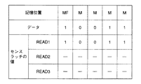
なお、データ(3回の読出後のデータラッチの値)と各動作によりセンスラッチ3にラッチされる値との関係は、図8に示されるようになる。
【0078】
これに対し、フラッシュメモリ1000では、図9〜図11に示される多値データの読出シーケンスを実行する。まず、制御用CPU16は、1回目の読出動作(READ1)で多値フラグMFのデータを読出し、この値に基づき、2回目および3回目の読出動作を行なうか否かを判断する。多値フラグMFのデータが“0”、すなわち同一セクタ(または同一ページ)のメモリセルMに多値データが記憶されていることを示す場合、2回目、3回目の読出動作READ2、READ3を実行する。READ1では、ワード線電圧を3.0V、READ2では、ワード線電圧を4.0V、READ3では、ワード線電圧を2.0Vにする。
【0079】
READ1では(図10(A)参照)、メモリセルアレイMAのメモリセルMおよび当該メモリセルMに対応する多値フラグMFのデータを読出す。メモリセルMのデータ(“1”、“1”、“0”、“0”)をセンスラッチ3♯1で、多値フラグMFのデータ(“0”)をセンスラッチ3♯2でラッチする。
【0080】
多値フラグMFのデータが“0”であるため、制御用CPU16は、多値データ読出用のシーケンスを実行する。センスラッチ3♯1からデータラッチ2にメモリセルMの反転データを転送する(転送処理)。
【0081】
READ2では(図10(B)参照)、メモリセルMからデータを読出す。メモリセルMのデータ( “1”、“0”、“0”、“0”)を、センスラッチ3♯1でラッチする。センスラッチ3♯1からデータラッチ1にメモリセルMのデータを転送する(転送処理)。
【0082】
READ3では(図10(C)参照)、メモリセルMからデータを読出す。メモリセルMのデータ( “1”、“1”、“1”、“0”)を、センスラッチ3♯1でラッチする。
【0083】
次に、演算処理を行なう(図11(A)参照)。演算処理では、メモリセルアレイMAのビット線に対して、センスラッチ3♯1に基づき選択プリチャージ処理を行ない、データラッチ1に基づき選択ディスチャージ処理を行なう。これにより、データラッチ1のデータとセンスラッチ3♯1のデータとのXOR処理が行なわれる。
【0084】
次に、出力処理を行なう(図11(B)参照)。具体的には、データラッチ1でセンス処理を行なう。データラッチ1に、メモリセルアレイMAのビット線の電位に対応するデータがラッチされる(“0”、“1”、“1”、“0”)。そして、データラッチ2のデータ(“0”、“0”、“1”、“1”)と、データラッチ1のデータを反転したデータとを出力する。これにより、多値データ(“01”、“00”、“10”、“11”)が読出されることになる。
【0085】
なお、データ(3回の読出動作の後のデータラッチの値)と各動作によりセンスラッチ3にラッチされる値との関係は、図12に示されるようになる。
【0086】
2値データの読出時には、フラッシュメモリ1000は、図13〜図14に示される2値データの読出シーケンスを実行する。制御用CPU16は、1回目の読出動作(READ1)で読出された多値フラグMFのデータが“1”であるならば、図13に示されるように、READ1で読出動作を終了する。
【0087】
READ1では(図14(A)参照)、メモリセルアレイMAのメモリセルMおよび当該メモリセルMに対応する多値フラグMFのデータを読出す。メモリセルMのデータ(“1”、“1”、“0”、“0”)をセンスラッチ3♯1で、多値フラグMFのデータ(“1”)をセンスラッチ3♯2でラッチする。
【0088】
多値フラグMFのデータが“1”であるため、制御用CPU16は、2値データ読出用のシーケンスを実行するように制御する。センスラッチ3♯1からデータラッチ2にデータを転送する(転送処理)。データラッチ2に、読出したデータの反転データがラッチされる。
【0089】
次に、出力処理を行なう(図14(B)参照)。具体的には、データラッチ2のデータ(“0”、“0”、“1”、“1”)を出力する。これにより、2値データ(“0”、“0”、“1”、“1”)が読出されることになる。
【0090】
なお、データ(1回の読出動作後のデータラッチの値)と1回の読出動作でセンスラッチ3にラッチされる値との関係は、図15に示されるようになる。このように、多値フラグの値に基づき、読出動作を1回で終了することができる。
【0091】
次にフラッシュメモリ1000へのデータの書込シーケンスについて、多値データのみを記憶する多値フラッシュメモリと比較しながら説明する。
【0092】
多値フラッシュメモリでは、図16〜図19に示される書込シーケンスを実行する。なお、多値データ(“01”、“00”、“10”または“11”)を、本願と同様、データラッチ1、2およびセンスラッチ3♯1を使用して書込むものとする。
【0093】
図16を参照して、3回の書込動作(PROGRAM1、PROGRAM2、PROGRAM3)を実行する。PROGRAM1では、ワード線電圧を18V、PROGRAM2では、ワード線電圧を17V、PROGRAM3では、ワード線電圧を16Vにする。
【0094】
PROGRAM1でデータ“01”が、PROGRAM2でデータ“00”が、PROGRAM3でデータ“10”が書込まれる。
【0095】
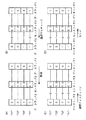
PROGRAM1の処理は、図17(A)〜(D)に示されるとおりである。図17(A)を参照して、データラッチ1に1ビット目のデータ(“1”、“0”、“0”、“1”)を、データラッチ2に2ビット目のデータ(“0”、“0”、“1”、“1”)を格納する。データラッチ1からセンスラッチ3にデータを転送する(転送処理)。
【0096】
図17(B)を参照して、データラッチ2とセンスラッチ3との間のビット線をすべてプリチャージする(“1”)。図17(C)を参照して、当該ビット線に対して、データラッチ2に基づき選択ディスチャージ処理を、センスラッチ3に基づき選択ディスチャージ処理を行なう。
【0097】
次に、図17(D)を参照して、センスラッチ3でセンス処理を行なう。センスラッチ3に、当該ビット線の電位に対応するデータ(“1”、“0”、“0”、“0”)および反転データがラッチされる。“0”をラッチしたセンスラッチに接続されるメモリセルMにデータ“01”が書込まれる。
【0098】
PROGRAM2の処理は、図18(A)〜(D)に示されるとおりである。図18(A)を参照して、データラッチ1からセンスラッチ3にデータを転送する(転送処理)。図18(B)を参照して、センスラッチ3に基づき、データラッチ2とセンスラッチ3との間のビット線に対して選択プリチャージ処理を行なう。図18(C)を参照して、データラッチ2に基づき、当該ビット線に対して選択ディスチャージ処理を行なう。図18(D)を参照して、センスラッチ3でセンス処理を行なう。センスラッチ3に、当該ビット線の電位に対応するデータ(“0”、“1”、“0”、“0”)および反転データがラッチされる。“0”をラッチしたセンスラッチに接続されるメモリセルMにデータ“00”が書込まれる。
【0099】
PROGRAM3の処理は、図19(A)〜(D)に示されるとおりである。図19(A)を参照して、データラッチ1からセンスラッチ3にデータを転送する(転送処理)。図19(B)を参照して、センスラッチ3とデータラッチ1との間のビット線をすべてプリチャージ(“1”)する。図19(C)を参照して、当該ビット線に対して、センスラッチ3に基づき選択ディスチャージ処理を、データラッチ1に基づき選択ディスチャージ処理を行なう。
【0100】
次に、図19(D)を参照して、センスラッチ3でセンス処理を行なう。センスラッチ3に、当該ビット線の電位に対応するデータ(“0”、“0”、“1”、“0”)および反転データがラッチされる。“0”をラッチしたセンスラッチに接続されるメモリセルMにデータ“10”が書込まれる。
【0101】
なお、データ(データロード後のデータラッチの値)と各動作でセンスラッチ3にラッチされる値との関係は、図20に示されるようになる。
【0102】
これに対し、フラッシュメモリ1000は、多値データの書込時には、図21〜図23に示される書込シーケンスを実行する。
【0103】
図21を参照して、3回の書込動作(PROGRAM1、PROGRAM2、PROGRAM3)を実行する。PROGRAM1では、ワード線電圧を18V、PROGRAM2では、ワード線電圧を17V、PROGRAM3では、ワード線電圧を16Vにする。
【0104】
PROGRAM1の処理は、図22(A)〜(D)に示されるとおりである。図22(A)を参照して、データラッチ1に1ビット目のデータ(“1”、“0”、“0”、“1”)を、データラッチ2に2ビット目のデータ(“0”、“0”、“1”、“1”)を格納する。データラッチ1からセンスラッチ3♯1にデータを転送する(転送処理)。
【0105】
同時に、メモリセルアレイMA側の多値フラグMFに“0”を書込むため、センスラッチ3♯2のメモリセルアレイMA側に“0”を格納する。
【0106】
図22(B)を参照して、メモリセルアレイMBのビット線をすべてプリチャージする(“1”)。図22(C)を参照して、メモリセルアレイMBのビット線に対して、データラッチ2に基づき選択ディスチャージ処理を、センスラッチ3♯1に基づき選択ディスチャージ処理を行なう。
【0107】
図22(D)を参照して、センスラッチ3♯1でセンス処理を行なう。センスラッチ3♯1に、当該ビット線の電位に対応するデータ(“1”、“0”、“0”、“0”)および反転データがラッチされる。“0”をラッチしたセンスラッチに接続されるメモリセルMにデータ“01”が書込まれる。
【0108】
PROGRAM2、3の処理内容は、上述した多値フラッシュメモリにおけるPROGRAM2、3の処理と同じである。これにより、データ“00”、“10”が書込まれる。
【0109】
なお、データ(データロード後のデータラッチの値)と各書込動作においてセンスラッチ3にラッチされる値との関係は、図23に示されるようになる。
【0110】
このように、多値データの書込時には、データラッチに書込データをラッチする。そして、多値データ“01”を書込むときは、対応するセンスラッチを“0”に、“01”以外の多値データに対応するメモリセルのセンスラッチを“1”にする。同様に、多値データ“00”を書込むときは、対応するセンスラッチを“0”に、“00”以外の多値データに対応するメモリセルのセンスラッチを“1”にする。さらに、多値データ“10”を書込むときは、対応するセンスラッチを“0”に、“10”以外の多値データに対応するメモリセルのセンスラッチを“1”にする。この際、多値フラグには、多値データであることを示す値を格納する。
【0111】
さらに、フラッシュメモリ1000は、2値データの書込時には、図24〜図25に示される書込シーケンスを実行する。
【0112】
図24を参照して、1回の書込動作(PROGRAM1)を実行する。PROGRAM1では、ワード線電圧を18Vにする。
【0113】
PROGRAM1の処理は、図25(A)〜(C)に示されるとおりである。図25(A)を参照して、データラッチ2に書込データ(“0”、“0”、“1”、“1”)を格納する。同時に、メモリセルアレイMA側の多値フラグMFに“1”を書込むため、センスラッチ3♯2のメモリセルアレイMA側に“1”を格納する。そして、メモリセルアレイMBのビット線をすべてプリチャージする(“1”)。
【0114】
図25(B)を参照して、メモリセルアレイMBのビット線に対して、データラッチ2に基づき選択ディスチャージ処理を行なう。図25(C)を参照して、センスラッチ3♯1でセンス処理を行なう。センスラッチ3♯1に、当該ビット線の電位に対応するデータ(“1”、“1”、“0”、“0”)および反転データがラッチされる。これにより、“0”をラッチしたセンスラッチに接続されるメモリセルMにデータ“0”(データ“01”に相当)が書込まれる。
【0115】
データ(データロード後のデータラッチの値)と1回の書込動作でセンスラッチ3にラッチされる値との関係は、図26に示されるようになる。
【0116】
このように、2値での書込み要求があった場合には、データ“01”を書込んだ時点で書込み動作を終了することができる。
【0117】
このように、本発明の実施の形態1によるフラッシュメモリ1000によると、多値データと2値データとを混在して記憶することができる。したがって、書込要求に応じて、たとえば、高い信頼性を必要とされるデータについては2値で記憶し、また大容量のデータは、多値で記憶することができる。また、多値データについては、多値で、2値データについては、2値でデータを読出すことができる。
【0118】
[実施の形態2]
本発明の実施の形態2では、フラッシュメモリ1000の改良例について説明する。本発明の実施の形態2による制御用CPU16は、2値データを読出す際も、多値データと同様、3回の読出動作を行なうように制御する。そして、1回目の読出動作と3回目の読出動作とで読出データの値が異なった場合、より具体的には、多値データの“10”、“00”に相当するしきい値になっている場合、2値で記憶させたデータのしきい値が変化していることを示す警告を発生する。
【0119】
警告が発生した場合、制御用CPU16は、2値データを再度書込むための制御を行なう。
【0120】
本発明の実施の形態2によるフラッシュメモリにおける2値データの読出シーケンスを、図28〜図31を用いて説明する。
【0121】
本発明の実施の形態2においては、図28に示されるように、合計3回の読出動作(READ1、READ2、READ3)を実行する。READ1では、ワード線電圧を3.0V、READ2では、ワード線電圧を4.0V、READ3では、ワード線電圧を2.0Vにする。
【0122】
2値データを書込んだメモリセルが、多値データ“01”の状態(“0P”)、多値データ“00”の状態(“0E”)、多値データ“11”の状態(“1P”)、または多値データ“10”の状態(“1E”)になったとする。制御用CPU16は、“0E”および“1E”の状態を検出し、警告を発生する。
【0123】
READ1では(図29(A)参照)、メモリセルアレイMAのメモリセルMおよび当該メモリセルMに対応する多値フラグMFのデータを読出し、センスラッチでラッチする。センスラッチ3♯1には、メモリセルM(“0P”、“0E”、“1E”、“1P”)に対応するデータ(“1”、“1”、“0”、“0”)が、センスラッチ3♯2のメモリセルアレイMA側には、多値フラグMFのデータ(“1”)が格納される。センスラッチ3♯1からデータラッチ2にデータを転送する(転送処理)。
【0124】
READ2では(図29(B)参照)、メモリセルMからデータを読出す。読出したデータ( “1”、“0”、“0”、“0”)を、センスラッチ3♯1でラッチする。センスラッチ3♯1からデータラッチ1にデータを転送する(転送処理)。
【0125】
READ3では(図29(C)参照)、メモリセルMからデータを読出す。読出したデータ( “1”、“1”、“1”、“0”)を、センスラッチ3♯1でラッチする。
【0126】
次に、演算処理を行なう(図29(D)参照)。演算処理では、メモリセルアレイMAのビット線に対して、センスラッチ3♯1に基づき選択プリチャージ処理を行ない、データラッチ1に基づき選択ディスチャージ処理を行なう。これにより、データラッチ1のデータとセンスラッチ3♯1のデータとのXOR処理が行なわれる。
【0127】
次に、出力処理を行なう(図29(E)参照)。具体的には、データラッチ1でセンス処理を行なう。データラッチ1に、メモリセルアレイMAのビット線の電位に対応するデータがラッチされる(“0”、“1”、“1”、“0”)。
【0128】
なお、データ(3回の読出動作の後のデータラッチの値)と各動作によりセンスラッチ3♯1にラッチされる値との関係は、図32に示されるようになる。
【0129】
制御用CPU16は、読出したデータが2値データの場合(多値フラグMFが“1”)、00レベル検出処理および10レベル検出処理をさらに行なう。
【0130】
00レベル検出処理では、第1処理として(図30(A)参照)、メモリセルアレイMAのビット線をすべてプリチャージする。第2処理では(図30(B)参照)、メモリセルアレイMAのビット線に対して、データラッチ1に基づき選択ディスチャージ処理を行ない、センスラッチ3♯1でセンス処理を行なう。
【0131】
第3処理では(図30(C)参照)、メモリセルアレイMBのビット線に対して、センスラッチ3♯1に基づき選択プリチャージ処理を行ない、データラッチ2に基づき選択ディスチャージ処理を行なう。さらに、第4処理として(図30(D)参照)、センスラッチ3♯1でセンス処理を行なう。センスラッチ3♯1に、メモリセルアレイMBのビット線の電位に対応するデータがラッチされる(“0”、“1”、“0”、“0”)。
【0132】
“0E”の状態のメモリセルに対応するセンスラッチには、他のメモリセルに対応するセンスラッチと異なる値が格納される。ラッチされた値を用いて、図33に示される全ラッチ判定回路200でALL判定処理を行なう。そして、00レベル検出処理の第4処理が終了すると、10レベル検出処理を行なう。
【0133】
10レベル検出処理の第1処理では(図31(A)参照)、データラッチ1からセンスラッチ3♯1にデータを転送する(転送処理)。続く第2処理では(図31(B)参照)、メモリセルアレイMBのビット線に対して、センスラッチ3♯1に基づき選択ディスチャージ処理を行ない、データラッチ2に基づき選択プリチャージ処理を行なう。
【0134】
続く第3処理では(図31(C)参照)、センスラッチ3♯1でセンス処理を行なう。センスラッチ3♯1に、メモリセルアレイMBのビット線の電位に対応するデータがラッチされる(“0”、“0”、“1”、“0”)。
【0135】
“1E”の状態のメモリセルに対応するセンスラッチには、他のメモリセルに対応するセンスラッチと異なる値が格納される。ラッチされた値を用いて、図33に示される全ラッチ判定回路200でALL判定処理を行なう。
【0136】
ALL判定処理を行なう全ラッチ判定回路200は、図33に示されるように、信号線Lと接地電圧を受けるノードとの間に設けれる複数のNMOSトランジスタT10、T11、T12、…、信号線Lと電源電圧を受けるノードとの間に設けられる抵抗素子R、ならびに信号線Lの信号を反転するインバータV20およびV21を含む。
【0137】
トランジスタT10、T11、T12、…は、複数のセンスラッチ3♯1のそれぞれに対応して設けられる。トランジスタT10、T11、T12、…のそれぞれは、対応するセンスラッチ3♯1の出力に応じてオン/オフする。
【0138】
すべてのセンスラッチ3♯1の出力が“L"レベルであれば、インバータV21から出力される判定値は、”H"レベルになる。
【0139】
したがって、図30および図31に示される場合、1つのセンスラッチ3♯1からHレベルの信号が出力されるため、判定値は“L”レベルになる。この判定値に基づき、制御用CPU16は、しきい値のずれを修正するため再度2値データの書込みを行うとともに、しきい値のずれを示す警告信号を発生する。警告信号は、たとえば、ステータスレジスタ18を介して外部に出力する。
【0140】
このように、本発明の実施の形態2によるフラッシュメモリによると、2値データを正確に記憶することができる。また、2値データのずれを検出した場合には、外部にずれの発生を知らせることができる。
【0141】
[実施の形態3]
本発明の実施の形態3では、フラッシュメモリ1000の改良例を示す。上述した実施の形態1では、2値データ“0”の書込要求があった場合、メモリセルを多値データ“01”の状態、すなわちしきい値が最も高い状態に設定する。
【0142】
これに対して、本発明の実施の形態3における制御用CPU16は、2値データ“0”の書込要求があった場合、メモリセルを、多値データ“11”の状態に最も近い多値データ“10”の状態に設定する(図43参照)。
【0143】
“01”に書込む場合よりも、しきい値のシフト量が少ないので、書込み時間を短縮することができる。この結果、本発明の実施の形態3によるフラッシュメモリによると、高速な書込動作が実現される。
【0144】
[実施の形態4]
本発明の実施の形態4によるデータ記憶システム4000について、図34を用いて説明する。データ記憶システム4000は、図34に示されるように、2値フラッシュメモリ102、多値フラッシュメモリ104Aおよび104B、ならびにカウンタ/タイマ401、バッファ402、コントローラ403、およびエラー訂正回路404を含むシステムコントローラ400を備える。
【0145】
2値フラッシュメモリ102は、複数の不揮発性メモリセルを含む。2値フラッシュメモリ102に含まれるメモリセルには2値データが書込まれ、また当該メモリセルからは2値データが読出される。
【0146】
多値フラッシュメモリ104Aおよび104Bのそれぞれは、複数の不揮発性メモリセルを含む。多値フラッシュメモリ104Aおよび104Bのそれぞれに含まれるメモリセルには多値データが書込まれ、また当該メモリセルからは多値データが読出される。
【0147】
2値フラッシュメモリ102、多値フラッシュメモリ104Aおよび104Bのそれぞれは、I/Oピンからデータを入出力する。I/Oピンは、バッファ402と接続されている。
【0148】
2値フラッシュメモリ102は、R/Bピンから動作中であるか否かを示す信号R/B0を出力する。多値フラッシュメモリ104Aおよび104Bのそれぞれは、R/Bピンから動作中であるか否かを示す信号R/B1、R/B2を出力する。信号R/B0、R/B1、R/B2は、コントローラ403に入力される。
【0149】
2値フラッシュメモリ102、多値フラッシュメモリ104Aおよび104Bのそれぞれは、コントローラ403から出力されるチップイネーブル信号を/OEピンで受けて動作する。
【0150】
カウンタ/タイマ401は、一定期間内にホストシステム4100から要求される書込データの大きさを測定する。カウンタ/タイマ401の測定結果は、コントローラ403に出力される。
【0151】
バッファ402は、ホストシステム4100から転送されるデータを取込み、またフラッシュメモリから読出されたデータを取込む。
【0152】
エラー訂正回路404は、コントローラ403の制御に基づき、バッファ402に取込まれた書込データに誤り訂正検出信号を付加し、またホストシステム4100への読出データの転送時に、バッファ402に取込まれたデータに対してエラー訂正処理を行なう。
【0153】
コントローラ403は、カウンタ/タイマ401の出力、信号R/B0、R/B1、R/B2をモニタして、フレッシュメモリへのデータの書込みを制御する。また、データの読出時、エラー訂正を行なうか否かを制御する。
【0154】
図35に示されるように、データ記憶システム4000を駆動するためのソフトウェア、FAT情報(フラッシュメモリのアドレスとデータ記憶システム4000におけるアドレスとの対応を示すファイル情報)および高速書込要求時のユーザデータは、相対的に高信頼性かつ高速動作が可能なフラッシュメモリ102に書込む。これら以外のユーザデータは、多値フラッシュメモリ104Aおよび104Bに書込む。
【0155】
システムコントローラ400によるフラッシュメモリへの書込制御の第1例について、多値フラッシュメモリのみを複数個配置したデータ記憶システムと対比して説明する。
【0156】
多値フラッシュメモリのみを用いる場合、図36に示される手順で書込みが行なわれる。なお、データ記憶システムが、多値フラッシュメモリをN個搭載しているものとする。N個の多値フラッシュメモリのそれぞれにデバイス番号1〜Nを割当てる。ホストシステムからの書込要求があると(ステップS401)、書込対象として指定するデバイス番号(DEVICE NO)を初期化“0”する(ステップS401)。
【0157】
続いて、デバイス番号を“1”インクリメントする(ステップS402)。対応する多値フラッシュメモリの信号R/Bに応じて、書込可能であるか(Ready状態)か、書込不可である(Busy状態)かを判断する(ステップS403)。
【0158】
書込可能(Ready状態)であれば、デバイス番号に対応する多値フラッシュメモリにホストシステムから受けるデータを書込む(ステップS404)。そして、ホストシステムからの次の書込要求を受付ける(ステップS400)。
【0159】
書込不可(Busy状態)であれば、デバイス番号が最大値“N”に達したか否かを判断する(ステップS405)。デバイス番号がNより小さければ、デバイス番号を“1”インクリメントする処理に移る(ステップS402)。デバイス番号が“N”である場合には、デバイス番号を初期化“0”する処理に移る(ステップS401)。このようにして、搭載される複数の多値フラッシュメモリのうち、書込可能なフラッシュメモリにデータを順次書込んでいく。
【0160】
一方、データ記憶システム4000によると、図37に示される手順で書込みが実行される。なお、データ記憶システム4000が、N個の多値フラッシュメモリと1個の2値フラッシュメモリとを搭載しているものとする。N個の多値フラッシュメモリのそれぞれにデバイス番号1〜Nを、2値フラッシュメモリにデバイス番号(N+1)を割当てる。
【0161】
ホストシステム4100から書込要求があると(ステップS410)、書込対象となるデバイス番号を初期化“0”する(ステップS411)。続いて、デバイス番号を“1”インクリメントする(ステップS412)。対応する多値フラッシュメモリの信号R/Bに応じて、書込可能であるか(Ready状態)か、書込不可である(Busy状態)かを判断する(ステップS413)。
【0162】
書込可能(ReadY状態)であれば、デバイス番号に対応するフラッシュメモリにデータを書込む(ステップS414)。そして、ホストシステム4100からの次の書込要求を受付ける(ステップS410)。
【0163】
書込不可(Busy状態)であれば、デバイス番号が最大値“N+1”に達したか否かを判断する(ステップS415)。デバイス番号が“N+1”より小さければ、デバイス番号を“1”インクリメントする処理に移る(ステップS412)。
【0164】
デバイス番号が“N+1”である場合には、対応するフラッシュメモリ(2値フラッシュメモリ)がReady状態かBusy状態であるかを判断する処理に移る(ステップS413)。
【0165】
すなわち、システムコントローラ400は、フラッシュメモリの状態(R/B)をモニタして、Ready状態の多値フラッシュメモリからデータの書込みを行なうよう制御する。そして、すべての多値フラッシュメモリがBusy状態になると、2値フラッシュメモリにデータを書込むように制御する。この動作により、データ記憶システム4000に、大容量のデータを格納することができる。
【0166】
システムコントローラ400によるフラッシュメモリへの書込制御の第2例について、図38を用いて説明する。図38を参照して、ホストシステム4100からの書込要求があるか否かを判断する(ステップS420)。書込要求がある場合には、後述するデータの大きさによる書込制御処理(ステップS421)に移る。
【0167】
書込要求が無い場合、2値フラッシュメモリ102に高速書込要求時のユーザデータが書込まれているか否かを判断する(ステップS422)。2値フラッシュメモリ102に高速書込要求時のユーザデータが無いときには、処理を行なわない(ステップS423)。2値フラッシュメモリ102に高速書込要求時のユーザデータが書込まれているときには、2値フラッシュメモリ102の当該データをバッファ402に転送させる(ステップS424)。
【0168】
バッファ402を介して、多値フラッシュメモリに当該データを書込む(ステップS425)。そして、ホストシステム4100の次の書込要求を判断する処理に移る(ステップS420)。
【0169】
すなわち、ホストシステム4100から書込要求が無いときには、2値フラッシュメモリ102に書込まれた高速書込要求時のユーザデータを多値フラッシュメモリに移し替える。これにより、高速書込と大容量とを両立させることができる。
【0170】
書込データの大きさによる書込制御処理(ステップS421)について、図39を用いて説明する。ホストシステム4100からの書込み要求があると(ステップS430)、カウンタ/タイマ401の出力に基づき、一定時間の大きさ(基準値)の書込データがあるか否かを判断する。書込データの大きさが基準値以内の場合、書込対象とするデバイス番号を初期化“0”する(ステップS432)。続いて、デバイス番号を“1”インクリメントして(ステップS433)、対応するフラッシュメモリのReady/Busy状態を判定する処理に移る(ステップS435)。
【0171】
書込データの大きさが基準値以上の場合、デバイス番号を“N+1”にして(ステップS434)、対応する2値フラッシュメモリのReady/Busy状態を判定する処理に移る(ステップS435)。
【0172】
対応するフラッシュメモリがReady状態であるならば、当該フラッシュメモリにデータを書込む(ステップS436)。そして、ホストシステム4100からの次の書込要求を受付ける(ステップS430)。
【0173】
対応するフラッシュメモリがBusy状態の場合、デバイス番号が最大値“N+1”に達したか否かを判断する(ステップS437)。デバイス番号が“N+1”より小さければ、デバイス番号を“1”インクリメントする処理に移る(ステップS433)。
【0174】
デバイス番号が“N+1”の場合、対応するフラッシュメモリ(2値フラッシュメモリ)がReady状態かBusy状態であるかを判断する処理に移る(ステップS435)。
【0175】
すなわち、システムコントローラ400は、データが大きい場合には高速なデータの書込が要求されていると判断して、高速動作が可能な2値フラッシュメモリに当該データを書込む。
【0176】
次に、システムコントローラ400によるフラッシュメモリの読出制御例について、図40を用いて説明する。ホストシステム4100からの読出要求があると(ステップS450)、フラッシュメモリに格納される対応するデータがバッファ402に転送される(ステップS451)。
【0177】
バッファ402に転送されたデータが、多値フラッシュメモリから読出された多値データであるか否かを判断する(ステップS452)。
【0178】
データが2値フラッシュメモリから読出された場合、エラー訂正回路404におけるエラー訂正処理を行なわず、バッファ402からホストシステム4100へデータを転送する処理に移る(ステップS456)。
【0179】
データが多値フラッシュメモリから読出された場合、バッファ402に転送されたデータをエラー訂正回路404に送る(ステップS453)。エラー訂正回路404においてエラー訂正処理が実施される(ステップS454)。エラー訂正後のデータは、バッファ402に格納する(ステップS455)。そして、バッファ402からホストシステム4100へデータを転送する処理に移る(ステップS456)。
【0180】
すなわち、2値フラッシュメモリへの書込み時には、誤り訂正符号を付けず、多値フラッシュメモリへの書込み時には、誤り訂正符号を付加しておく。そして、ホストシステム4100からのデータ読出要求に対し、高信頼性の2値フラッシュメモリからデータを読出した場合には、エラー訂正を行なわず、多値フラッシュメモリからデータを読出した場合には、エラー訂正を行なってからホストシステム4100にデータを転送するよう制御する。これにより、高速動作を実現することができる。
【0181】
[実施の形態5]
本発明の実施の形態5によるデータ記憶システム5000について、図41を用いて説明する。データ記憶システム5000は、図41に示されるように、多値/2値フラッシュメモリ100A、100Bおよび100C、ならびにシステムコントローラ400を含む。多値/2値フラッシュメモリ100A〜100Cは、実施の形態1、2または3で説明した構成を有し、メモリセルに2値データまたは多値データを記憶させることができる。
【0182】
実施の形態5による構成の場合、図42に示されるように、フラッシュメモリ100A、100Bに、ユーザデータを多値データで、高速書込要求時のユーザデータを2値データで書込み、フラッシュメモリ100Cに、ユーザデータを多値データで、高速書込要求時のユーザデータ、データ記憶システムを駆動するためのソフトウェアおよびFAT情報(フラッシュメモリのアドレスとデータ記憶システム5000におけるアドレスとの対応を示すファイル情報)を2値データで書込むことができる。
【0183】
システムコントローラ400は、ホストシステム4100から受ける書込みデータの種類に応じて、多値で記憶させるか2値で記憶させるかを制御する。また、システムコントローラ400は、データの種類に応じて、エラー訂正を行なう否かを制御することも可能である。
【0184】
また、書込要求が無い場合、フラッシュメモリに高速書込要求時のユーザデータ(2値データ)が書込まれているときには、当該データをバッファ402に転送させ、バッファ402を介して、多値の状態で当該データを記憶させることも可能である。
【0185】
実施の形態4の場合、2値フラッシュメモリ102に未使用領域が多く残っているにもかかわらず多値フラッシュメモリには未使用領域が無くなり、または、多値フラッシュメモリに未使用領域が多く残っているにもかかわらず2値フラッシュメモリ102には未使用領域が無くなることもあり得る。
【0186】
そこで、本発明の実施の形態5では、多値データ/2値データを書込み、書込んだ多値データ/値データを読出すことができるフラッシュメモリを配置する。これにより、メモリ空間を有効に使用しつつ、信頼性の高いかつ高速動作が行なうことが可能になる。
【0187】
今回開示された実施の形態はすべての点で例示であって制限的なものではないと考えられるべきである。本発明の範囲は、上記した実施の形態の説明ではなくて特許請求の範囲によって示され、特許請求の範囲と均等の意味および範囲内でのすべての変更が含まれることが意図される。
【0188】
【発明の効果】
請求項1および2に係る不揮発性半導体記憶装置によると、要求に応じて、2値データまたは3以上の多値データを書込み、読出すことができる。これにより、大容量のデータを記憶しつつ、必要に応じて、高信頼性かつ高速にデータを書込みかつ読出すことができる。
【0189】
請求項1に係る不揮発性半導体記憶装置は、2値データを記憶したメモリセルに対して、しきい値のずれを検出することができる。
【0190】
請求項2に係る不揮発性半導体記憶装置は、2値データを記憶したメモリセルに対して、しきい値のずれを検出した場合、再度2値データを書込み(データ修復)することができる。
【0191】
請求項3に係る不揮発性半導体記憶装置は、請求項1または2に係る不揮発性半導体記憶装置であって、書込/読出単位(セクタ、ページ)毎にフラグを配置する。これにより、2値データを書込んだか多値データを書込んだかを示す値をフラグに格納することができる。
【0192】
請求項4に係る不揮発性半導体記憶装置は、請求項3に係る不揮発性半導体記憶装置であって、フラグをメモリセルと同じ構造とする。これにより、メモリセルの書込/読出と同時に、フラグに対する書込/読出を行なうことが容易にできる。
【0193】
請求項5に係る不揮発性半導体記憶装置は、請求項3に係る不揮発性半導体記憶装置であって、メモリセルへの書込みと同時に、フラグに、メモリセルに2値データを書込んだか多値データを書込んだかを記憶させることができる。
【0194】
請求項6に係る不揮発性半導体記憶装置は、請求項3に係る不揮発性半導体記憶装置であって、外部から2値データの書込要求がある場合には、2値データの書込シーケンスを、外部から多値データの書込要求がある場合には、多値データの書込シーケンスを実行することができる。
【0195】
請求項7に係る不揮発性半導体記憶装置は、請求項3に係る不揮発性半導体記憶装置であって、フラグに基づき、書込/読出単位ごとに、2値データまたは多値データを読出すことができる。
【図面の簡単な説明】
【図1】 本発明の実施の形態1によるフラッシュメモリ1000の全体構成の概要を示すブロック図である。
【図2】 フラッシュメモリ1000の主要部の構成を示す回路図である。
【図3】 信号処理回路25の構成について説明するための回路図である。
【図4】 (A)〜(C)は、選択プリチャージ処理・選択ディスチャージ処理・センス処理における信号の状態を示す図である。
【図5】 多値フラッシュメモリの読出動作時におけるワード線電圧を示す図である。
【図6】 (A)〜(C)は、多値フラッシュメモリにおける読出シーケンス(READ1〜READ3)を示す図である。
【図7】 (A)および(B)は、多値フラッシュメモリにおける読出シーケンスを示す図である。
【図8】 多値フラッシュメモリの読出動作時におけるデータとセンスラッチの値との関係を示す図である。
【図9】 フラッシュメモリ1000の多値データ読出動作時におけるワード線電圧を示す図である。
【図10】 (A)〜(C)は、フラッシュメモリ1000における多値データの読出シーケンス(READ1〜READ3)を示す図である。
【図11】 (A)および(B)は、フラッシュメモリ1000における多値データの読出シーケンスを示す図である。
【図12】 フラッシュメモリ1000の多値データ読出動作時におけるデータとセンスラッチの値との関係を示す図である。
【図13】 フラッシュメモリ1000の2値データ読出動作時におけるワード線電圧を示す図である。
【図14】 (A)および(B)は、フラッシュメモリ1000における2値データの読出シーケンスについて説明するための図である。
【図15】 フラッシュメモリ1000の2値データ読出動作時におけるデータとセンスラッチの値との関係を示す図である。
【図16】 多値フラッシュメモリの書込動作時におけるワード線電圧を示す図である。
【図17】 (A)〜(D)は、多値フラッシュメモリにおける書込シーケンス(PROGRAM1)について説明するための図である。
【図18】 (A)〜(D)は、多値フラッシュメモリにおける書込シーケンス(PROGRAM2)について説明するための図である。
【図19】 (A)〜(D)は、多値フラッシュメモリにおける書込シーケンス(PROGRAM3)について説明するための図である。
【図20】 多値フラッシュメモリの書込動作時におけるデータとセンスラッチの値との関係を示す図である。
【図21】 フラッシュメモリ1000の多値データ書込動作時におけるワード線電圧を示す図である。
【図22】 (A)〜(D)は、フラッシュメモリ1000における多値データの書込シーケンス(PROGRAM1)を示す図である。
【図23】 フラッシュメモリ1000の多値データ書込動作時におけるデータとセンスラッチの値との関係を示す図である。
【図24】 フラッシュメモリ1000の2値データ書込動作時におけるワード線電圧を示す図である。
【図25】 (A)〜(C)は、フラッシュメモリ1000における2値データの書込シーケンス(PROGRAM1)を示す図である。
【図26】 フラッシュメモリ1000の2値データ書込動作時におけるデータとセンスラッチの値との関係を示す図である。
【図27】 (A)〜(D)は、フラッシュメモリ1000の書込/消去/読出時における電圧関係を説明するための図である。
【図28】 本発明の実施の形態2によるフラッシュメモリの2値データ読出時におけるワード線電圧を示す図である。
【図29】 (A)〜(E)は、本発明の実施の形態2によるフラッシュメモリにおける2値データの読出シーケンスを示す図である。
【図30】 (A)〜(D)は、本発明の実施の形態2における00レベル検出処理の内容を示す図である。
【図31】 (A)〜(C)は、本発明の実施の形態2における10レベル検出処理の内容を示す図である。
【図32】 2値データ読出動作時におけるデータとセンスラッチの値との関係を示す図である。
【図33】 全ラッチ判定回路200の構成を示す回路図である。
【図34】 本発明の実施の形態4によるデータ記憶システム4000について説明するための図である。
【図35】 データ記憶システム4000におけるアドレス空間上のデータ配置例を示す図である。
【図36】 多値フラッシュメモリのみを複数個配置したデータ記憶システムにおける書込制御を示すフローチャートである。
【図37】 データ記憶システム4000における第1の書込制御を示すフローチャートである。
【図38】 データ記憶システム4000における第2の書込制御を示すフローチャートである。
【図39】 データ記憶システム4000における書込データの大きさによる書込制御処理を示すフローチャートである。
【図40】 データ記憶システム4000における読出制御を示すフローチャートである。
【図41】 本発明の実施の形態5によるデータ記憶システム5000について説明するための図である。
【図42】 データ記憶システム5000におけるアドレス空間上のデータ配置例を示す図である。
【図43】 多値データと2値データとの関係を示す図である。
【図44】 不揮発性メモリセルにおける多値データと2値データとの関係を示す図である。
【符号の説明】
1,2 データラッチ、3♯1,3♯2 センスラッチ、11 入出力バッファ、12 アドレスデコーダ、13 コマンドデコーダ、14A,14B Xデコーダ、15A,15B 多値フラグ部、16 制御用CPU、17 ベリファイ回路、18 ステータスレジスタ、19,20 Yデコーダ/データラッチ、21 Yデコーダ/センスラッチ、22 多値フラグセンスラッチ部、25 信号処理部、100A〜100C 多値/2値フラッシュメモリ、102 2値フラッシュメモリ、104A,104B 多値フラッシュメモリ、400 システムコントローラ、401 カウンタ/タイマ、402 バッファ402 コントローラ、404 エラー訂正回路、1000 フラッシュメモリ、4000 データ記憶システム、4100 ホストシステム、MA,MB メモリセルアレイ、M メモリセル、MF 多値フラグ。[0001]
BACKGROUND OF THE INVENTION
The present invention relates to a nonvolatile semiconductor memory device and a data storage system, and more particularly to a configuration using an electrically writable / erasable nonvolatile semiconductor memory cell.
[0002]
[Prior art]
Non-volatile semiconductor memory (flash memory) that can be electrically written and erased is widely used as an alternative to EPROM and mask ROM as a program code storage memory, taking advantage of the fact that it can be rewritten on the substrate. did.
[0003]
In recent years, as semiconductor processing technology has been miniaturized, a large-capacity flash memory capable of storing image data and audio data has appeared, and its application to digital still cameras and portable audio is rapidly progressing.
[0004]
However, the flash memory is required to have a larger capacity in order to enable recording of moving image data.
[0005]
As an important technology for realizing a larger capacity of the flash memory, there is a multi-value technology in addition to the miniaturization of the semiconductor processing technology. A flash memory generally stores data by changing a threshold value of a memory cell by applying a high electric field to a floating gate insulated from the surroundings by an insulating film and injecting or discharging electric charges.
[0006]
In the case of a normal flash memory (binary flash memory), the high threshold value of the memory is “1” (or “0”), and the low threshold value of the memory cell is “0” (or “1”). ).
[0007]
In the case of a flash memory using a multi-value technology (multi-value flash memory), the threshold value of the memory cell is set to a plurality of states of 3 or more. For example, in a flash memory capable of storing four values, the threshold value of the memory cell is set to four states, and “11” (the lowest threshold state), “10”, “00”, Correspond to “01” (the state with the highest threshold). Thereby, 2-bit data can be stored in one memory cell. Needless to say, the correspondence between the physical state of the memory cell and the logical data can be arbitrarily determined as in the binary flash memory.
[0008]
[Problems to be solved by the invention]
By the way, when realizing a multi-value flash memory, if “1” (or “0”) is stored in a memory cell and the data is read after being left for a long time, it becomes “0” (or “1”). There is an important problem of becoming.
[0009]
This problem is physically caused by electrons injected into the floating gate being emitted to the semiconductor substrate or gate through the energy barrier to the insulating film or by being injected from the semiconductor substrate or gate. This happens because the threshold of changes.
[0010]
Referring to FIG. 44, in the case of a binary flash memory, for example, the threshold value in the “1” state is set to 1 V to 1.7 V, the threshold value in the “0” state is set to 4.3 V or more, and determination at the time of reading is performed. The threshold is 3V. In this case, there is a read margin of 1.3 V in both the “1” state and the “0” state. In this case, erroneous reading occurs when electrons corresponding to 1.3 V are injected / released.
[0011]
On the other hand, in the case of a multi-level flash memory, for example, the threshold value in the “11” state is 1 V to 1.7 V, the threshold value in the “10” state is 2.3 V to 2.7 V, and the “00” state is The threshold value is set to 3.3 V to 3.7 V, and the threshold value in the “01” state is set to 4.3 V or more. If the determination threshold value at the time of reading is 2V, 3V, and 4V, the reading margin in each state is only 0.3V. Therefore, when electrons corresponding to 0.3 V are injected / released, erroneous reading occurs.
[0012]
Vgs-I represented by F1 in FIG. d The memory cell having the s characteristic emits electrons from the floating gate, whereby Vgs-I represented by F2. d In the same state as the memory cell having the s characteristic, in the multilevel flash memory, the written data “01” is erroneously read as “00”.
[0013]
Similarly, Vgs-I represented by F3 d A memory cell having the s characteristic is represented by Vgs-I represented by F4. d In the same state as the memory cell having the s characteristic, in the multi-level flash memory, the written data “11” is erroneously read as “10”.
[0014]
On the other hand, in the binary flash memory, even when the memory cell in the F1 state is in the F2 state or the memory cell in the F3 state is in the F4 state, data is read correctly. .
[0015]
As described above, the multilevel flash memory and the binary flash memory have data retention characteristics that are physically equivalent to each other, but the data reliability of the binary flash memory is superior to that of the multilevel flash memory. Yes. In terms of data transfer speed, the binary flash memory is superior. On the other hand, as described above, the multilevel flash memory is superior in terms of cost and capacity increase. Therefore, in the future, it will be required to develop devices that effectively utilize all these characteristics.
[0016]
Accordingly, the present invention has been made to solve such a problem, and an object of the present invention is to realize a non-volatile semiconductor memory device and a data storage that realize a large capacity of the memory and that can perform data reliability and high-speed operation. To provide a system.
[0017]
[Means for Solving the Problems]
A semiconductor memory device according to one aspect of the present invention includes a nonvolatile memory cell array including a plurality of memory cells, and a control circuit for controlling a write operation, a read operation, and an erase operation with respect to the plurality of memory cells. In response to a write request, the circuit writes binary data or multi-value data of three or more values to a memory cell to be written, and at the time of a read operation, depending on the written contents of the memory cell to be read, Read binary data or multi-value data.
[0018]
Preferably, the control circuit sets the memory cell to be written to any one of a first state which is an erased state or an nth state different from the first state when binary data is written. When multi-value data is written, any one of a total of n (three or more) different states from the first state to the n-th state is set. Further, in the read operation, the control circuit, from the first state to the kth state (where k <n) or from the (k + 1) state to the nth state, for the memory cell into which binary data has been written. It is determined to which of the memory cells the multi-value data is written, and it is determined to which of the total n states the memory cell is written.
In particular, when the memory cell into which binary data is written belongs to a total of n states during a read operation, and when it is determined that the memory cell belongs to a state different from the first state or the nth state A warning signal indicating that the binary data has changed is output to the outside. Alternatively, in the read operation, when it is determined which of the total n states the memory cell into which binary data has been written belongs, and it is determined that the memory cell belongs to a state different from the first state or the nth state Then, a write operation for writing the binary data again to the memory cell is performed.
[0019]
Preferably, the plurality of memory cells are collectively divided into a plurality of write / read units to be subjected to a write operation and a read operation, and a plurality of memory cells arranged for each of the plurality of write / read units. A flag is further provided, and each of the plurality of flags stores a value indicating whether binary data has been written or multi-value data has been written to the memory cell of the corresponding write / read unit. In particular, the flag has the same structure as the memory cell.
[0020]
In particular, in the write operation, the control circuit writes binary data or multi-value data in the write / read unit to be written, and simultaneously writes the binary data to the corresponding flag. Write a value indicating whether it was written.
[0021]
In particular, the control circuit writes a first write sequence or multi-value data for writing binary data to a write / read unit to be written in response to a write request received from the outside. A second write sequence is executed for recording. In the read operation, the control circuit, when binary data is written in the write / read unit to be read based on the value of the flag corresponding to the write / read unit to be read. A first read sequence for reading binary data is executed, and if multi-value data is written, a second read sequence for reading multi-value data is executed.
[0022]
Preferably, each of the plurality of memory cells has a total of n states (n is 3 or more) different from each other, including a first state that is an erased state and a second state that is closest to the first state. When writing binary data, the control circuit sets the memory cell to be written to the first state or the second state, and when reading binary data, the memory cell to be read is set to the first state or the second state. It is determined which of the n states in total does not belong to the first state.
[0023]
A data storage system according to a further aspect of the present invention includes a memory region including a first non-volatile semiconductor memory having a first characteristic and a second non-volatile semiconductor memory having a second characteristic different from the first characteristic; And a control device for writing data in the memory region and reading data from the memory region, the control device according to the stored data to be written to the memory region received from the outside, It is determined whether writing that conforms to the first characteristic or writing that conforms to the second characteristic is required, and the stored data is stored in the first nonvolatile semiconductor memory or the second nonvolatile semiconductor memory according to the determination. Write.
[0024]
Preferably, the first characteristic is a characteristic capable of storing data with predetermined reliability and operating at a predetermined processing speed, and is relatively higher than the first characteristic. It is a characteristic that can store data with reliability and can operate at a higher speed than the first characteristic.
[0025]
Preferably, the first nonvolatile semiconductor memory includes a plurality of multi-value data memory cells each storing data of 2 bits or more, and the second nonvolatile semiconductor memory includes a plurality of data each storing 1-bit data. Memory cells.
[0026]
Preferably, the second nonvolatile memory is used when it is determined that writing of data that requires relatively high reliability in the memory area or transferring data at high speed is required from the outside according to stored data. In other cases, the stored data is written in the first nonvolatile semiconductor memory.
[0027]
Preferably, the control device stores the stored data in the second nonvolatile semiconductor memory if the first nonvolatile semiconductor memory is in operation, and in the first nonvolatile semiconductor memory if the first nonvolatile semiconductor memory is not in operation. Write stored data.
[0028]
Preferably, the control device receives a measurement circuit for measuring the size of stored data received from the outside within a certain period of time, and receives the output of the measurement circuit. And a circuit for controlling the storage data to be written to the second nonvolatile semiconductor memory when the stored data is written to the nonvolatile semiconductor memory and the size of the stored data exceeds the reference value.
[0029]
Preferably, the control device transfers data already written in the second nonvolatile semiconductor memory to the first nonvolatile semiconductor memory in response to no data exchange with the outside.
[0030]
Preferably, the control device writes management data for managing the memory area in the second nonvolatile semiconductor memory.
[0031]
Preferably, an error correction circuit for adding an error detection code to the data is further provided, and the controller adds the error detection code to the write data and writes the stored data when writing the stored data to the first nonvolatile semiconductor memory. When the stored data is written to the second nonvolatile semiconductor memory, writing is performed without adding an error detection code to the write data.
[0032]
A data storage system according to a further aspect of the present invention includes a non-volatile memory region including a plurality of memory cells, and each of the plurality of memory cells stores and stores data in a binary state or a multi-value state of three or more values. Controller for reading out binary or multi-valued data, exchanging data with the outside, writing data in nonvolatile memory area and reading data from nonvolatile memory area When the control device determines that it is requested from the outside to write data that requires relatively high reliability or to exchange data at high speed according to the stored data, 2 Write the stored data to the nonvolatile memory area in the value state.
[0033]
Preferably, the control device receives a measurement circuit for measuring the size of stored data received from the outside within a certain period of time, and receives the output of the measurement circuit, and if the size of the stored data is equal to or less than a reference value, the control device And a circuit for controlling the storage data to be written into the nonvolatile memory area in a multi-valued state and when the size of the stored data exceeds the reference value, the storage data is written to the nonvolatile memory area in a binary state. .
[0034]
In particular, the control device writes management data for managing the memory area in a binary state in the nonvolatile memory area.
[0035]
Preferably, the control device includes an error correction circuit for adding an error detection code to the data, and when the control device writes data in a multivalued state, the control device adds the error detection code and performs writing. When writing data in the state of values, writing is performed without adding an error detection code.
[0036]
DETAILED DESCRIPTION OF THE INVENTION
Hereinafter, embodiments of the present invention will be described in detail with reference to the drawings. In the drawings, the same or corresponding parts are denoted by the same reference numerals and description thereof will not be repeated.
[0037]
[Embodiment 1]
A
[0038]
Referring to FIG. 1,
[0039]
The plurality of pins are an R / B pin P1 that outputs a signal R / B indicating whether the memory is operating (Busy state) or is operable (Ready state), and data for inputting and outputting data It includes an input / output pin group P2 and a control pin group P3 that receives an external control signal for controlling internal operations. Control pin group P3 includes a / CE pin that receives a chip enable / CE signal.
[0040]
Memory cells included in memory cell arrays MA and MB can be set in a plurality of states, and store binary data or multi-value data (three or more values). In the following description, “01”, “00”, “10”, “11” will be used as an example of multi-value data. The correspondence shown in FIG. 44 is applied to the relationship between the multi-value data / binary data and the threshold value. In the first embodiment, when there is a write request for binary data “0”, the memory cell is brought into a state of multi-value data “01”.
[0041]
The
[0042]
A command received from the outside controls whether data is stored in binary or multi-value in the memory cell. The
[0043]
Reading / writing is performed in units of sectors (or pages) composed of memory cells connected to one word line.
[0044]
The
[0045]
As will be described later, the
[0046]
Referring to FIG. 2, memory cell array MA includes a plurality of nonvolatile memory cells M and word lines WL00 and WL01 arranged in the row direction. Memory cell array MB includes a plurality of nonvolatile memory cells M and word lines WL10 and WL11 arranged in the row direction. Bit lines BL1 and BL2 are arranged in common corresponding to the columns of memory cell arrays MA and MB.
[0047]
The control gate layer of the memory cell M is connected to the word line, the drain region is connected to the bit line, and the source region receives the source voltage VSL.
[0048]
[0049]
Each of the
[0050]
Y decoder /
[0051]
Y decoder /
[0052]
Each of the drains of the memory cells connected to one word line is electrically connected to a different sense latch and data latch.
[0053]
During the read operation, a read voltage is applied to the word line, and it is determined whether or not a current flows through the memory cell via the sense latch. The data latches 1 and 2 are used for saving the read result. In the first embodiment of the present invention, data latches 1 and 2 are arranged to read a 2-bit signal from one memory cell. Data is output to the outside using the values of the data latches 1 and 2.
[0054]
In the write operation, first, data is input to data latches 1 and 2, and then a value is set in
[0055]
Multi-level flag
[0056]
A
[0057]
As shown in FIG. 3, the
[0058]
The transistor T1 is arranged between the bit line and the input / output node Z1 of the latch L. Transistor T2 is connected between nodes Z2 and Z3, and has a gate connected to node Z1. Transistor T3 is connected between node Z3 and the bit line.
[0059]
The
[0060]
In the selective precharge process, as shown in FIG. 4A, an L level signal is applied to the gate of the transistor T1, an H level signal is applied to the node Z2, and an H level signal is applied to the gate of the transistor T3. If the value latched in the latch L is “1”, the bit line is held at “H” by the
[0061]
In the selective discharge process, as shown in FIG. 4B, an L level signal is applied to the gate of the transistor T1, an L level signal is applied to the node Z2, and an H level signal is applied to the gate of the transistor T3. If the value latched in the latch L is “1”, the bit line is held at “L”, and if “0”, the bit line holds the voltage level as it is.
[0062]
Further, in the sense processing, as shown in FIG. 4C, an H level signal is applied to the gate of the transistor T1, an H or L level signal is applied to the node Z2, and an L level signal is applied to the gate of the transistor T3. To do. The latch L becomes “1” or “0” depending on the potential of the bit line.
[0063]
The data transfer process from latch to latch shown below is realized by performing a selective precharge process based on the transfer source latch and performing a sense process in the transfer destination latch.
[0064]
An outline of writing / reading / erasing of the
[0065]
At the time of data writing, as shown in FIG. 27A, a positive high voltage (for example, 18 V) is applied to control
[0066]
As shown in FIG. 27B, for a memory cell that is not a write target, the corresponding sense latch is set to “1” (6 V) and 6 V is applied to the
[0067]
At the time of batch erasing of data, a negative high voltage (for example, −16 V) is applied to the
[0068]
When data is read, a positive voltage (for example, 3 V) is applied to control
[0069]
Next, details of the data reading sequence in the
[0070]
In the multilevel flash memory, the read sequence shown in FIGS. 5 to 7 is executed. Note that multi-value data (“01”, “00”, “10” or “11”) is read using the data latches 1 and 2 and the
[0071]
Referring to FIG. 5, three read operations (READ1, READ2, and READ3) are executed. In READ1, the word line voltage is set to 3.0V, in READ2, the word line voltage is set to 4.0V, and in READ3, the word line voltage is set to 2.0V.
[0072]
In READ 1 (see FIG. 6A), data is read from the memory cell array, and the read data (“1”, “1”, “0”, “0”) is latched by the
[0073]
In READ 2 (see FIG. 6B), data is read from the memory cell array, and the read data (“1”, “0”, “0”, “0”) is latched by the
[0074]
In READ 3 (see FIG. 6C), data is read from the memory cell array, and the read data (“1”, “1”, “1”, “0”) is latched by the
[0075]
Next, arithmetic processing is performed (see FIG. 7A). In the arithmetic processing, data is transferred from the
[0076]
Next, an output process is performed (FIG. 7B). Specifically, data is transferred from the
[0077]
The relationship between the data (value of the data latch after three readings) and the value latched in the
[0078]
On the other hand, the
[0079]
In READ1 (see FIG. 10A), data of the memory cell M of the memory cell array MA and the multilevel flag MF corresponding to the memory cell M are read. The data (“1”, “1”, “0”, “0”) of the memory cell M is latched by the
[0080]
Since the data of the multi-value flag MF is “0”, the
[0081]
In READ2 (see FIG. 10B), data is read from the memory cell M. Data (“1”, “0”, “0”, “0”) of the memory cell M is latched by the
[0082]
In READ3 (see FIG. 10C), data is read from the memory cell M. Data (“1”, “1”, “1”, “0”) of memory cell M is latched by
[0083]
Next, arithmetic processing is performed (see FIG. 11A). In the arithmetic processing, selective precharge processing is performed on the bit lines of the memory cell array MA based on the
[0084]
Next, an output process is performed (see FIG. 11B). Specifically, the
[0085]
The relationship between the data (value of the data latch after three read operations) and the value latched in the
[0086]
At the time of reading binary data, the
[0087]
In READ1 (see FIG. 14A), data of the memory cell M of the memory cell array MA and the multilevel flag MF corresponding to the memory cell M are read. The data (“1”, “1”, “0”, “0”) of the memory cell M is latched by the
[0088]
Since the data of the multilevel flag MF is “1”, the
[0089]
Next, an output process is performed (see FIG. 14B). Specifically, data (“0”, “0”, “1”, “1”) of the data latch 2 is output. As a result, binary data (“0”, “0”, “1”, “1”) is read out.
[0090]
Note that the relationship between the data (value of the data latch after one read operation) and the value latched in the
[0091]
Next, a data write sequence to the
[0092]
In the multilevel flash memory, the write sequence shown in FIGS. 16 to 19 is executed. It is assumed that multi-value data (“01”, “00”, “10” or “11”) is written using data latches 1 and 2 and
[0093]
Referring to FIG. 16, three write operations (PROGRAM1, PROGRAM2, and PROGRAM3) are executed. In PROGRAM1, the word line voltage is set to 18V, in PROGRAM2, the word line voltage is set to 17V, and in PROGRAM3, the word line voltage is set to 16V.
[0094]
Data “01” is written in PROGRAM1, data “00” is written in PROGRAM2, and data “10” is written in PROGRAM3.
[0095]
The processing of
[0096]
Referring to FIG. 17B, all the bit lines between
[0097]
Next, referring to FIG. 17D, the
[0098]
The processing of PROGRAM2 is as shown in FIGS. Referring to FIG. 18A, data is transferred from data latch 1 to sense latch 3 (transfer processing). Referring to FIG. 18B, a selective precharge process is performed on the bit line between
[0099]
The processing of
[0100]
Next, referring to FIG. 19D, the
[0101]
The relationship between the data (value of the data latch after data loading) and the value latched in the
[0102]
On the other hand,
[0103]
Referring to FIG. 21, three write operations (PROGRAM1, PROGRAM2, and PROGRAM3) are executed. In PROGRAM1, the word line voltage is set to 18V, in PROGRAM2, the word line voltage is set to 17V, and in PROGRAM3, the word line voltage is set to 16V.
[0104]
The processing of PROGRAM1 is as shown in FIGS. 22 (A) to (D). Referring to FIG. 22A, data latch 1 has the first bit data (“1”, “0”, “0”, “1”), and data latch 2 has the second bit data (“0”). ”,“ 0 ”,“ 1 ”,“ 1 ”). Data is transferred from data latch 1 to sense
[0105]
At the same time, “0” is written to the memory cell array MA side of the
[0106]
Referring to FIG. 22B, all the bit lines of memory cell array MB are precharged (“1”). Referring to FIG. 22C, selective discharge processing is performed on the bit lines of memory cell array MB based on
[0107]
Referring to FIG. 22D, sense processing is performed in
[0108]
The processing contents of PROGRAM2 and 3 are the same as the processing of PROGRAM2 and 3 in the multi-level flash memory described above. Thereby, data “00” and “10” are written.
[0109]
The relationship between the data (value of the data latch after data loading) and the value latched in the
[0110]
Thus, when writing multi-value data, the write data is latched in the data latch. When the multi-value data “01” is written, the corresponding sense latch is set to “0”, and the sense latch of the memory cell corresponding to the multi-value data other than “01” is set to “1”. Similarly, when writing multi-value data “00”, the corresponding sense latch is set to “0”, and the sense latch of the memory cell corresponding to multi-value data other than “00” is set to “1”. Further, when multi-value data “10” is written, the corresponding sense latch is set to “0”, and the sense latch of the memory cell corresponding to multi-value data other than “10” is set to “1”. At this time, a value indicating multi-value data is stored in the multi-value flag.
[0111]
Further, the
[0112]
Referring to FIG. 24, one write operation (PROGRAM1) is executed. In PROGRAM1, the word line voltage is set to 18V.
[0113]
The processing of
[0114]
Referring to FIG. 25B, selective discharge processing is performed on the bit lines of memory cell array MB based on
[0115]
The relationship between the data (value of the data latch after data loading) and the value latched in the
[0116]
As described above, when there is a binary write request, the write operation can be terminated when the data “01” is written.
[0117]
Thus, according to the
[0118]
[Embodiment 2]
In the second embodiment of the present invention, an improved example of the
[0119]
When a warning occurs, the
[0120]
A binary data read sequence in the flash memory according to the second embodiment of the present invention will be described with reference to FIGS.
[0121]
In
[0122]
The memory cell into which binary data has been written is in a state of multi-value data “01” (“0P”), a state of multi-value data “00” (“0E”), a state of multi-value data “11” (“1P ”) Or the state of multi-value data“ 10 ”(“ 1E ”). The
[0123]
In READ1 (see FIG. 29A), the data of the memory cell M of the memory cell array MA and the multilevel flag MF corresponding to the memory cell M are read and latched by the sense latch. Data (“1”, “1”, “0”, “0”) corresponding to the memory cell M (“0P”, “0E”, “1E”, “1P”) is stored in the
[0124]
In READ2 (see FIG. 29B), data is read from the memory cell M. The read data (“1”, “0”, “0”, “0”) is latched by the
[0125]
In READ3 (see FIG. 29C), data is read from the memory cell M. The read data (“1”, “1”, “1”, “0”) is latched by the
[0126]
Next, arithmetic processing is performed (see FIG. 29D). In the arithmetic processing, selective precharge processing is performed on the bit lines of the memory cell array MA based on the
[0127]
Next, an output process is performed (see FIG. 29E). Specifically, the
[0128]
The relationship between the data (value of the data latch after the three read operations) and the value latched in the
[0129]
When the read data is binary data (multi-value flag MF is “1”), the
[0130]
In the 00 level detection process, as the first process (see FIG. 30A), all the bit lines of the memory cell array MA are precharged. In the second process (see FIG. 30B), a selective discharge process is performed on the bit lines of memory cell array MA based on
[0131]
In the third process (see FIG. 30C), a selective precharge process is performed on the bit lines of the memory cell array MB based on the
[0132]
The sense latch corresponding to the memory cell in the “0E” state stores a value different from that of the sense latch corresponding to another memory cell. Using the latched value, ALL determination processing is performed by all the
[0133]
In the first process of the 10-level detection process (see FIG. 31A), data is transferred from the data latch 1 to the
[0134]
In the subsequent third process (see FIG. 31C), the
[0135]
The sense latch corresponding to the memory cell in the “1E” state stores a value different from that of the sense latch corresponding to the other memory cell. Using the latched value, ALL determination processing is performed by all the
[0136]
As shown in FIG. 33, all latch
[0137]
Transistors T10, T11, T12,... Are provided corresponding to each of the plurality of sense latches 3 # 1. Each of transistors T10, T11, T12,... Is turned on / off according to the output of the
[0138]
If the outputs of all sense latches 3 # 1 are at "L" level, the determination value output from inverter V21 is at "H" level.
[0139]
Therefore, in the case shown in FIGS. 30 and 31, since the H level signal is output from one
[0140]
Thus, according to the flash memory according to the second embodiment of the present invention, binary data can be accurately stored. In addition, when the deviation of the binary data is detected, the occurrence of the deviation can be notified to the outside.
[0141]
[Embodiment 3]
In the third embodiment of the present invention, an improved example of the
[0142]
On the other hand, when there is a write request for binary data “0”, the
[0143]
Since the threshold shift amount is smaller than in the case of writing to “01”, the writing time can be shortened. As a result, the flash memory according to the third embodiment of the present invention realizes a high-speed write operation.
[0144]
[Embodiment 4]
A
[0145]
The
[0146]
Each of
[0147]
Each of the
[0148]
The
[0149]
Each of the
[0150]
The counter /
[0151]
[0152]
Based on the control of the
[0153]
The
[0154]
As shown in FIG. 35, software for driving the
[0155]
A first example of writing control to the flash memory by the
[0156]
When only the multi-level flash memory is used, writing is performed according to the procedure shown in FIG. It is assumed that the data storage system is equipped with N multi-value flash memories.
[0157]
Subsequently, the device number is incremented by “1” (step S402). It is determined whether writing is possible (Ready state) or writing is not possible (Busy state) in accordance with the signal R / B of the corresponding multi-level flash memory (Step S403).
[0158]
If it is writable (Ready state), the data received from the host system is written into the multilevel flash memory corresponding to the device number (step S404). Then, the next write request from the host system is accepted (step S400).
[0159]
If writing is not possible (Busy state), it is determined whether or not the device number has reached the maximum value “N” (step S405). If the device number is smaller than N, the process proceeds to a process of incrementing the device number by “1” (step S402). If the device number is “N”, the process proceeds to processing for initializing the device number to “0” (step S401). In this way, data is sequentially written into a writable flash memory among a plurality of mounted multi-value flash memories.
[0160]
On the other hand, according to the
[0161]
When there is a write request from the host system 4100 (step S410), the device number to be written is initialized to “0” (step S411). Subsequently, the device number is incremented by “1” (step S412). It is determined whether writing is possible (Ready state) or writing is impossible (Busy state) in accordance with the signal R / B of the corresponding multilevel flash memory (Step S413).
[0162]
If it is writable (ReadY state), data is written into the flash memory corresponding to the device number (step S414). Then, the next write request from the
[0163]
If writing is not possible (Busy state), it is determined whether or not the device number has reached the maximum value “N + 1” (step S415). If the device number is smaller than “N + 1”, the process proceeds to a process of incrementing the device number by “1” (step S412).
[0164]
When the device number is “N + 1”, the process proceeds to processing for determining whether the corresponding flash memory (binary flash memory) is in the Ready state or the Busy state (step S413).
[0165]
That is, the
[0166]
A second example of writing control to the flash memory by the
[0167]
If there is no write request, it is determined whether or not the user data at the time of the high-speed write request is written in the binary flash memory 102 (step S422). If there is no user data at the time of the high-speed write request in the
[0168]
The data is written to the multi-value flash memory via the buffer 402 (step S425). Then, the process proceeds to processing for determining the next write request of the host system 4100 (step S420).
[0169]
That is, when there is no write request from the
[0170]
The write control process (step S421) based on the size of the write data will be described with reference to FIG. When there is a write request from the host system 4100 (step S430), based on the output of the counter /
[0171]
If the size of the write data is greater than or equal to the reference value, the device number is set to “N + 1” (step S434), and the process proceeds to processing for determining the ready / busy state of the corresponding binary flash memory (step S435).
[0172]
If the corresponding flash memory is in the Ready state, data is written to the flash memory (step S436). Then, the next write request from the
[0173]
If the corresponding flash memory is in the Busy state, it is determined whether or not the device number has reached the maximum value “N + 1” (step S437). If the device number is smaller than “N + 1”, the process proceeds to a process of incrementing the device number by “1” (step S433).
[0174]
If the device number is “N + 1”, the process proceeds to processing for determining whether the corresponding flash memory (binary flash memory) is in the Ready state or the Busy state (step S435).
[0175]
That is, the
[0176]
Next, an example of flash memory read control by the
[0177]
It is determined whether the data transferred to the
[0178]
If the data is read from the binary flash memory, the error correction process in the
[0179]
When the data is read from the multilevel flash memory, the data transferred to the
[0180]
That is, no error correction code is added when writing to the binary flash memory, and an error correction code is added when writing to the multilevel flash memory. In response to a data read request from the
[0181]
[Embodiment 5]
A
[0182]
In the case of the configuration according to the fifth embodiment, as shown in FIG. 42, the user data is written to the
[0183]
The
[0184]
Further, when there is no write request, when the user data (binary data) at the time of the high-speed write request is written in the flash memory, the data is transferred to the
[0185]
In the case of the fourth embodiment, although there are many unused areas remaining in the
[0186]
Therefore, in the fifth embodiment of the present invention, a flash memory is provided which can write multi-value data / binary data and read the written multi-value data / value data. This makes it possible to perform a highly reliable and high-speed operation while effectively using the memory space.
[0187]
The embodiment disclosed this time should be considered as illustrative in all points and not restrictive. The scope of the present invention is shown not by the above description of the embodiment but by the scope of claims for patent, and is intended to include all modifications within the meaning and scope equivalent to the scope of claims for patent.
[0188]
【The invention's effect】
[0189]
[0190]
[0191]
Claim 3 A non-volatile semiconductor memory device according to
[0192]
Claim 4 The nonvolatile semiconductor memory device according to
[0193]
Claim 5 The nonvolatile semiconductor memory device according to
[0194]
[0195]
[Brief description of the drawings]
FIG. 1 is a block diagram showing an outline of an overall configuration of a
FIG. 2 is a circuit diagram showing a configuration of a main part of the
FIG. 3 is a circuit diagram for explaining a configuration of a
4A to 4C are diagrams illustrating signal states in a selective precharge process, a selective discharge process, and a sense process.
FIG. 5 is a diagram showing a word line voltage during a read operation of a multilevel flash memory.
6A to 6C are diagrams showing a read sequence (READ1 to READ3) in a multi-level flash memory. FIG.
7A and 7B are diagrams showing a read sequence in a multi-level flash memory. FIG.
FIG. 8 is a diagram showing the relationship between data and the value of a sense latch during a read operation of a multilevel flash memory.
FIG. 9 is a diagram showing a word line voltage during a multi-value data read operation of the
10A to 10C are diagrams showing a multi-value data read sequence (READ1 to READ3) in the
11A and 11B are diagrams showing a multi-value data read sequence in the
FIG. 12 is a diagram showing a relationship between data and a value of a sense latch during a multi-value data read operation of the
13 is a diagram showing a word line voltage during binary data read operation of the
FIGS. 14A and 14B are diagrams for explaining a binary data read sequence in the
15 is a diagram showing the relationship between data and the value of a sense latch during binary data read operation of the
FIG. 16 is a diagram showing a word line voltage during a write operation of the multi-level flash memory.
FIGS. 17A to 17D are diagrams for describing a write sequence (PROGRAM1) in a multi-level flash memory.
FIGS. 18A to 18D are diagrams for explaining a write sequence (PROGRAM2) in a multi-level flash memory.
FIGS. 19A to 19D are diagrams for explaining a write sequence (PROGRAM3) in the multi-level flash memory.
FIG. 20 is a diagram showing a relationship between data and a value of a sense latch during a write operation of a multi-level flash memory.
FIG. 21 is a diagram showing a word line voltage during a multi-value data write operation of the
22A to 22D are diagrams showing a multi-value data write sequence (PROGRAM1) in the
FIG. 23 is a diagram showing a relationship between data and a value of a sense latch during a multi-value data write operation of the
FIG. 24 is a diagram showing a word line voltage at the time of binary data write operation of the
FIGS. 25A to 25C are diagrams showing a binary data write sequence (PROGRAM1) in the
FIG. 26 is a diagram showing the relationship between the data and the value of the sense latch during the binary data write operation of the
FIGS. 27A to 27D are diagrams for explaining a voltage relationship during writing / erasing / reading of the
FIG. 28 is a diagram showing a word line voltage at the time of binary data reading of the flash memory according to the second embodiment of the present invention.
FIGS. 29A to 29E are diagrams showing a binary data read sequence in the flash memory according to the second embodiment of the present invention; FIGS.
FIGS. 30A to 30D are diagrams showing the contents of 00 level detection processing in the second embodiment of the present invention.
FIGS. 31A to 31C are diagrams showing the contents of 10-level detection processing in
FIG. 32 is a diagram showing a relationship between data and a sense latch value in a binary data read operation;
33 is a circuit diagram showing a configuration of all
FIG. 34 is a diagram for explaining a
FIG. 35 is a diagram showing an example of data arrangement in an address space in the
FIG. 36 is a flowchart showing write control in a data storage system in which a plurality of multi-value flash memories are arranged.
FIG. 37 is a flowchart showing first write control in the
38 is a flowchart showing second write control in the
FIG. 39 is a flowchart showing a write control process according to the size of write data in the
40 is a flowchart showing read control in the
FIG. 41 is a diagram for explaining a
42 is a diagram showing an example of data arrangement on an address space in the
FIG. 43 is a diagram illustrating a relationship between multi-value data and binary data.
FIG. 44 is a diagram showing a relationship between multi-value data and binary data in a nonvolatile memory cell.
[Explanation of symbols]
1, 2 Data latch, 3 # 1, 3 # 2 Sense latch, 11 Input / output buffer, 12 Address decoder, 13 Command decoder, 14A, 14B X decoder, 15A, 15B Multi-level flag section, 16 Control CPU, 17 Verify Circuit, 18 status register, 19, 20 Y decoder / data latch, 21 Y decoder / sense latch, 22 multi-level flag sense latch unit, 25 signal processing unit, 100A to 100C multi-level / binary flash memory, 102 binary flash Memory, 104A, 104B Multi-level flash memory, 400 system controller, 401 counter / timer, 402
Claims (7)
前記複数のメモリセルに対する書込動作、読出動作および消去動作を制御するための制御回路とを備え、
前記制御回路は、
書込要求に応じて、書込対象となるメモリセルに2値データまたは3値以上の多値データを書込み、前記読出動作時、読出対象となるメモリセルの書込内容に応じて、前記2値データまたは前記多値データを読出し、
前記書込対象となるメモリセルを、前記2値データの書込みの際には、消去状態である第1状態または前記第1状態と異なる第n状態のいずれか1つに設定し、前記多値データの書込みの際には、前記第1状態から前記第n状態までの互いに異なる合計n個(3個以上)の状態のうちいずれか1つに設定し、
前記読出動作時、前記2値データを書込んだメモリセルについては、前記第1状態から第k状態(ただし、k<n)まで、または第(k+1)状態から前記第n状態までのいずれに属するかを判定し、前記多値データを書込んだメモリセルについては、前記合計n個の状態のうちのいずれに属するかを判定し、
前記読出動作時、前記2値データを書込んだメモリセルが前記合計n個の状態のうちのいずれに属するかを判定し、前記第1状態または前記第n状態と異なる状態に属すると判定された場合に、外部に前記2値データが変化したことを示す警告信号を出力する、不揮発性半導体記憶装置。A non-volatile memory cell array including a plurality of memory cells;
A control circuit for controlling a write operation, a read operation and an erase operation for the plurality of memory cells,
The control circuit includes:
In response to a write request, binary data or multi-valued data of three or more values is written to a memory cell to be written, and at the time of the read operation, the 2 and reading the value data or the multi-value data,
When writing the binary data, the memory cell to be written is set to either the first state which is an erased state or the nth state different from the first state, and the multivalue When writing data, set to any one of a total of n (three or more) different states from the first state to the nth state,
During the read operation, the memory cell into which the binary data has been written is either from the first state to the kth state (where k <n) or from the (k + 1) state to the nth state. Determine whether the memory cell to which the multi-value data is written belongs to which of the total n states,
During the read operation, it is determined which of the total n states the memory cell into which the binary data has been written belongs, and is determined to belong to a state different from the first state or the nth state. A nonvolatile semiconductor memory device that outputs a warning signal indicating that the binary data has changed to the outside .
前記複数のメモリセルに対する書込動作、読出動作および消去動作を制御するための制御回路とを備え、
前記制御回路は、
書込要求に応じて、書込対象となるメモリセルに2値データまたは3値以上の多値データを書込み、前記読出動作時、読出対象となるメモリセルの書込内容に応じて、前記2値データまたは前記多値データを読出し、
前記書込対象となるメモリセルを、前記2値データの書込みの際には、消去状態である第1状態または前記第1状態と異なる第n状態のいずれか1つに設定し、前記多値データの書込みの際には、前記第1状態から前記第n状態までの互いに異なる合計n個(3個以上)の状態のうちいずれか1つに設定し、
前記読出動作時、前記2値データを書込んだメモリセルについては、前記第1状態から第k状態(ただし、k<n)まで、または第(k+1)状態から前記第n状態までのいずれに属するかを判定し、前記多値データを書込んだメモリセルについては、前記合計n個の状態のうちのいずれに属するかを判定し、
前記読出動作時、前記2値データを書込んだメモリセルが前記合計n個の状態のうちのいずれに属するかを判定し、前記第1状態または前記第n状態と異なる状態に属すると判定された場合に、前記メモリセルに対して再度前記2値データを書込むための書込動作を行なう、不揮発性半導体記憶装置。A non-volatile memory cell array including a plurality of memory cells;
A control circuit for controlling a write operation, a read operation and an erase operation for the plurality of memory cells,
The control circuit includes:
In response to a write request, binary data or multi-valued data of three or more values is written to a memory cell to be written, and at the time of the read operation, the 2 and reading the value data or the multi-value data,
When writing the binary data, the memory cell to be written is set to either the first state which is an erased state or the nth state different from the first state, and the multivalue When writing data, set to any one of a total of n (three or more) different states from the first state to the nth state ,
During the read operation, the memory cell into which the binary data has been written is either from the first state to the kth state (where k <n) or from the (k + 1) state to the nth state. Determine whether the memory cell to which the multi-value data is written belongs to which of the total n states ,
During the read operation, it is determined which of the total n states the memory cell into which the binary data has been written belongs, and is determined to belong to a state different from the first state or the nth state. A nonvolatile semiconductor memory device that performs a write operation to write the binary data again to the memory cell .
一括して前記書込動作および前記読出動作の対象となる複数の書込/読出単位に分割され、
前記複数の書込/読出単位のそれぞれに対して配置される複数のフラグをさらに備え、
前記複数のフラグのそれぞれは、
対応する書込/読出単位のメモリセルに前記2値データを書込んだか、前記多値データを書込んだかを示す値を格納する、請求項1または2に記載の不揮発性半導体記憶装置。The plurality of memory cells include
Divided into a plurality of write / read units to be subjected to the write operation and the read operation collectively,
A plurality of flags arranged for each of the plurality of write / read units;
Each of the plurality of flags is
3. The nonvolatile semiconductor memory device according to claim 1, wherein a value indicating whether the binary data is written or the multi-value data is written in a corresponding memory cell of a writing / reading unit is stored.
前記メモリセルと同じ構造を有する、請求項3に記載の不揮発性半導体記憶装置。The flag is
The nonvolatile semiconductor memory device according to claim 3 , wherein the nonvolatile semiconductor memory device has the same structure as the memory cell.
前記書込動作において、前記書込対象となる書込/読出単位に前記2値データまたは前記多値データを書込むと同時に、対応するフラグに前記2値データを書込んだか前記多値データを書込んだかを示す値を書込む、請求項3に記載の不揮発性半導体記憶装置。The control circuit includes:
In the write operation, the binary data or the multi-value data is written in the write / read unit to be written, and at the same time, the binary data is written in the corresponding flag. 4. The nonvolatile semiconductor memory device according to claim 3 , wherein a value indicating whether data has been written is written.
外部から受ける前記書込要求に応じて、前記書込対象となる書込/読出単位に対して、前記2値データを書込むための第1書込シーケンス、または前記多値データを書込むための第2書込シーケンスを実行する、請求項3に記載の不揮発性半導体記憶装置。The control circuit includes:
To write the binary data or the multi-value data to the write / read unit to be written in response to the write request received from the outside The nonvolatile semiconductor memory device according to claim 3 , wherein the second write sequence is executed.
前記読出動作において、前記読出対象となる書込/読出単位に対応するフラグの値に基づき、前記読出対象となる書込/読出単位に前記2値データが書込まれている場合には、前記2値データを読出すための第1読出シーケンスを、前記多値データが書込まれている場合には、前記多値データを読出すための第2読出シーケンスを実行する、請求項3に記載の不揮発性半導体記憶装置。The control circuit includes:
In the reading operation, when the binary data is written to the writing / reading unit to be read based on the value of the flag corresponding to the writing / reading unit to be read, a first read sequence for reading binary data, wherein when the multi-value data is written performs the second read sequence for reading the multi-valued data, according to claim 3 Nonvolatile semiconductor memory device.
Priority Applications (5)
| Application Number | Priority Date | Filing Date | Title |
|---|---|---|---|
| JP2000014557A JP4282197B2 (en) | 2000-01-24 | 2000-01-24 | Nonvolatile semiconductor memory device |
| US09/615,073 US6353553B1 (en) | 2000-01-24 | 2000-07-12 | Nonvolatile semiconductor memory device having structure storing multivalued data and data storage system comprising the nonvolatile semiconductor memory device |
| KR10-2000-0054397A KR100406612B1 (en) | 2000-01-24 | 2000-09-16 | Nonvolatile semiconductor memory device having structure storing multivalued data and data storage system comprising the nonvolatile semiconductor memory device |
| DE10046022A DE10046022A1 (en) | 2000-01-24 | 2000-09-18 | A nonvolatile semiconductor memory device having a structure for storing multivalued data and a data storage system including this nonvolatile semiconductor memory device |
| TW089119222A TW484060B (en) | 2000-01-24 | 2000-09-19 | Nonvolatile semiconductor memory device and data storage system comprising the nonvolatile semiconductor memory device |
Applications Claiming Priority (1)
| Application Number | Priority Date | Filing Date | Title |
|---|---|---|---|
| JP2000014557A JP4282197B2 (en) | 2000-01-24 | 2000-01-24 | Nonvolatile semiconductor memory device |
Related Child Applications (1)
| Application Number | Title | Priority Date | Filing Date |
|---|---|---|---|
| JP2008316900A Division JP4916504B2 (en) | 2008-12-12 | 2008-12-12 | Data storage system |
Publications (3)
| Publication Number | Publication Date |
|---|---|
| JP2001210082A JP2001210082A (en) | 2001-08-03 |
| JP2001210082A5 JP2001210082A5 (en) | 2006-11-09 |
| JP4282197B2 true JP4282197B2 (en) | 2009-06-17 |
Family
ID=18542004
Family Applications (1)
| Application Number | Title | Priority Date | Filing Date |
|---|---|---|---|
| JP2000014557A Expired - Fee Related JP4282197B2 (en) | 2000-01-24 | 2000-01-24 | Nonvolatile semiconductor memory device |
Country Status (5)
| Country | Link |
|---|---|
| US (1) | US6353553B1 (en) |
| JP (1) | JP4282197B2 (en) |
| KR (1) | KR100406612B1 (en) |
| DE (1) | DE10046022A1 (en) |
| TW (1) | TW484060B (en) |
Families Citing this family (84)
| Publication number | Priority date | Publication date | Assignee | Title |
|---|---|---|---|---|
| JP4299428B2 (en) * | 2000-01-19 | 2009-07-22 | 三星電子株式会社 | Variable capacity semiconductor memory device |
| JP2001209574A (en) * | 2000-01-25 | 2001-08-03 | Mitsubishi Electric Corp | Method for controlling storage device |
| US6297988B1 (en) * | 2000-02-25 | 2001-10-02 | Advanced Micro Devices, Inc. | Mode indicator for multi-level memory |
| JP2003022687A (en) * | 2001-07-09 | 2003-01-24 | Mitsubishi Electric Corp | Semiconductor memory |
| US6717847B2 (en) | 2001-09-17 | 2004-04-06 | Sandisk Corporation | Selective operation of a multi-state non-volatile memory system in a binary mode |
| US7554842B2 (en) * | 2001-09-17 | 2009-06-30 | Sandisk Corporation | Multi-purpose non-volatile memory card |
| US6839826B2 (en) | 2002-02-06 | 2005-01-04 | Sandisk Corporation | Memory device with pointer structure to map logical to physical addresses |
| JP2003242787A (en) | 2002-02-14 | 2003-08-29 | Mitsubishi Electric Corp | Nonvolatile semiconductor memory device |
| JP2004086991A (en) * | 2002-08-27 | 2004-03-18 | Renesas Technology Corp | Nonvolatile storage device |
| JP2004240795A (en) * | 2003-02-07 | 2004-08-26 | Renesas Technology Corp | Nonvolatile storage device |
| JP2005108304A (en) * | 2003-09-29 | 2005-04-21 | Toshiba Corp | Semiconductor memory and its control method |
| KR100719380B1 (en) | 2006-03-31 | 2007-05-18 | 삼성전자주식회사 | Multi-valued nonvolatile memory device with enhanced reliability and memory system having the same |
| US7881133B2 (en) | 2003-11-11 | 2011-02-01 | Samsung Electronics Co., Ltd. | Method of managing a flash memory and the flash memory |
| EP1538525A1 (en) * | 2003-12-04 | 2005-06-08 | Texas Instruments Incorporated | ECC computation simultaneously performed while reading or programming a flash memory |
| US7535759B2 (en) * | 2004-06-04 | 2009-05-19 | Micron Technology, Inc. | Memory system with user configurable density/performance option |
| US8082382B2 (en) * | 2004-06-04 | 2011-12-20 | Micron Technology, Inc. | Memory device with user configurable density/performance |
| US7336531B2 (en) | 2004-06-25 | 2008-02-26 | Micron Technology, Inc. | Multiple level cell memory device with single bit per cell, re-mappable memory block |
| JP2008020937A (en) * | 2004-10-29 | 2008-01-31 | Matsushita Electric Ind Co Ltd | Nonvolatile storage device |
| US7308525B2 (en) * | 2005-01-10 | 2007-12-11 | Sandisk Il Ltd. | Method of managing a multi-bit cell flash memory with improved reliablility and performance |
| JP4768298B2 (en) * | 2005-03-28 | 2011-09-07 | 株式会社東芝 | Nonvolatile semiconductor memory device |
| US7404028B2 (en) * | 2005-06-30 | 2008-07-22 | Gm Global Technology Operations, Inc. | ECU identification retention across reprogramming events |
| US7272041B2 (en) * | 2005-06-30 | 2007-09-18 | Intel Corporation | Memory array with pseudo single bit memory cell and method |
| US7752382B2 (en) * | 2005-09-09 | 2010-07-06 | Sandisk Il Ltd | Flash memory storage system and method |
| KR101162739B1 (en) * | 2005-09-29 | 2012-07-05 | 트렉 2000 인터네셔널 엘티디. | Portable data storage using SLC and MLC flash memory |
| JP2007109352A (en) | 2005-10-17 | 2007-04-26 | Matsushita Electric Ind Co Ltd | Nonvolatile semiconductor memory apparatus and its drive method |
| US7345914B2 (en) * | 2005-12-22 | 2008-03-18 | Intel Corporation | Use of flash memory blocks outside of the main flash memory array |
| JP2007200388A (en) * | 2006-01-24 | 2007-08-09 | Megachips Lsi Solutions Inc | Semiconductor memory device and its use method |
| JP2008009919A (en) * | 2006-06-30 | 2008-01-17 | Toshiba Corp | Card controller |
| JP4886434B2 (en) * | 2006-09-04 | 2012-02-29 | 株式会社東芝 | Nonvolatile semiconductor memory device |
| JP5072301B2 (en) * | 2006-09-25 | 2012-11-14 | 株式会社東芝 | Semiconductor integrated circuit device and operation method thereof |
| KR100827695B1 (en) | 2006-11-03 | 2008-05-07 | 삼성전자주식회사 | Non-volatile semiconductor memory device using weak cells as reading identifier |
| JP5028967B2 (en) * | 2006-11-15 | 2012-09-19 | 富士通セミコンダクター株式会社 | Semiconductor memory device and method for controlling semiconductor memory device |
| KR100791006B1 (en) | 2006-12-06 | 2008-01-03 | 삼성전자주식회사 | Semiconductor memory device having single-level cells and multi-level cells and driving method for the same |
| KR100794311B1 (en) | 2006-12-27 | 2008-01-11 | 삼성전자주식회사 | Program method of blocking program error for multi bit flash memory device |
| KR100799688B1 (en) | 2007-01-03 | 2008-02-01 | 삼성전자주식회사 | Memory system having back circuit and program method thereof |
| KR100872186B1 (en) * | 2007-01-04 | 2008-12-09 | 삼성전자주식회사 | Hybrid flash memory device with different error control scheme and memory system includign the same |
| JP5111882B2 (en) * | 2007-02-09 | 2013-01-09 | 株式会社東芝 | Nonvolatile semiconductor memory device |
| US7646636B2 (en) | 2007-02-16 | 2010-01-12 | Mosaid Technologies Incorporated | Non-volatile memory with dynamic multi-mode operation |
| US7675783B2 (en) * | 2007-02-27 | 2010-03-09 | Samsung Electronics Co., Ltd. | Nonvolatile memory device and driving method thereof |
| JP5224706B2 (en) * | 2007-03-23 | 2013-07-03 | キヤノン株式会社 | Storage device and storage device control method |
| JP2008257773A (en) * | 2007-04-02 | 2008-10-23 | Toshiba Corp | Nonvolatile semiconductor memory device, method for controlling the same, nonvolatile semiconductor memory system, and memory card |
| US7460398B1 (en) * | 2007-06-19 | 2008-12-02 | Micron Technology, Inc. | Programming a memory with varying bits per cell |
| KR101303177B1 (en) * | 2007-06-22 | 2013-09-17 | 삼성전자주식회사 | Non-volatile memory device and operating method of the same |
| JP2009104729A (en) | 2007-10-24 | 2009-05-14 | Toshiba Corp | Nonvolatile semiconductor memory device |
| KR101227368B1 (en) | 2007-11-05 | 2013-01-29 | 삼성전자주식회사 | Method for data programming of a NAND flash memory device and method for data reading of the same |
| JP2009129477A (en) * | 2007-11-20 | 2009-06-11 | Toshiba Corp | Nonvolatile semiconductor storage device |
| US7843728B2 (en) | 2007-11-20 | 2010-11-30 | Kabushiki Kaisha Toshiba | Nonvolatile semiconductor storage device |
| TWI404076B (en) * | 2008-01-07 | 2013-08-01 | Powerchip Technology Corp | Memory devices and data read method |
| US7755939B2 (en) * | 2008-01-15 | 2010-07-13 | Micron Technology, Inc. | System and devices including memory resistant to program disturb and methods of using, making, and operating the same |
| CN101911207B (en) | 2008-01-16 | 2014-05-07 | 富士通株式会社 | Semiconductor storage device, controlling apparatus and controlling method |
| CN101494086B (en) * | 2008-01-24 | 2011-12-07 | 群联电子股份有限公司 | Memory device, controller and switching method for flash memory |
| JP2009252255A (en) * | 2008-04-01 | 2009-10-29 | Renesas Technology Corp | Nonvolatile semiconductor memory device |
| US8060719B2 (en) | 2008-05-28 | 2011-11-15 | Micron Technology, Inc. | Hybrid memory management |
| KR101515098B1 (en) | 2008-11-20 | 2015-04-24 | 삼성전자주식회사 | Flash memory device and reading method thereof |
| US8102705B2 (en) * | 2009-06-05 | 2012-01-24 | Sandisk Technologies Inc. | Structure and method for shuffling data within non-volatile memory devices |
| US8027195B2 (en) * | 2009-06-05 | 2011-09-27 | SanDisk Technologies, Inc. | Folding data stored in binary format into multi-state format within non-volatile memory devices |
| US20110002169A1 (en) | 2009-07-06 | 2011-01-06 | Yan Li | Bad Column Management with Bit Information in Non-Volatile Memory Systems |
| CN102576708B (en) | 2009-10-30 | 2015-09-23 | 株式会社半导体能源研究所 | Semiconductor device |
| KR101752348B1 (en) * | 2009-10-30 | 2017-06-29 | 가부시키가이샤 한도오따이 에네루기 켄큐쇼 | Semiconductor device |
| WO2011062058A1 (en) * | 2009-11-20 | 2011-05-26 | Semiconductor Energy Laboratory Co., Ltd. | Semiconductor device |
| US8144512B2 (en) | 2009-12-18 | 2012-03-27 | Sandisk Technologies Inc. | Data transfer flows for on-chip folding |
| US8468294B2 (en) * | 2009-12-18 | 2013-06-18 | Sandisk Technologies Inc. | Non-volatile memory with multi-gear control using on-chip folding of data |
| US8725935B2 (en) | 2009-12-18 | 2014-05-13 | Sandisk Technologies Inc. | Balanced performance for on-chip folding of non-volatile memories |
| US20110153912A1 (en) * | 2009-12-18 | 2011-06-23 | Sergey Anatolievich Gorobets | Maintaining Updates of Multi-Level Non-Volatile Memory in Binary Non-Volatile Memory |
| JP5556189B2 (en) * | 2010-01-20 | 2014-07-23 | ソニー株式会社 | Storage device and data writing method |
| US9342446B2 (en) | 2011-03-29 | 2016-05-17 | SanDisk Technologies, Inc. | Non-volatile memory system allowing reverse eviction of data updates to non-volatile binary cache |
| JP2012212487A (en) * | 2011-03-30 | 2012-11-01 | Toshiba Corp | Memory system |
| US8588003B1 (en) * | 2011-08-01 | 2013-11-19 | Densbits Technologies Ltd. | System, method and computer program product for programming and for recovering from a power failure |
| JP2012043530A (en) * | 2011-10-24 | 2012-03-01 | Toshiba Corp | Nonvolatile semiconductor memory device |
| JP2013131275A (en) * | 2011-12-22 | 2013-07-04 | Toshiba Corp | Nonvolatile semiconductor memory device |
| US8842473B2 (en) | 2012-03-15 | 2014-09-23 | Sandisk Technologies Inc. | Techniques for accessing column selecting shift register with skipped entries in non-volatile memories |
| US8681548B2 (en) | 2012-05-03 | 2014-03-25 | Sandisk Technologies Inc. | Column redundancy circuitry for non-volatile memory |
| US9490035B2 (en) | 2012-09-28 | 2016-11-08 | SanDisk Technologies, Inc. | Centralized variable rate serializer and deserializer for bad column management |
| US9076506B2 (en) | 2012-09-28 | 2015-07-07 | Sandisk Technologies Inc. | Variable rate parallel to serial shift register |
| US8897080B2 (en) | 2012-09-28 | 2014-11-25 | Sandisk Technologies Inc. | Variable rate serial to parallel shift register |
| KR102068342B1 (en) * | 2013-03-07 | 2020-01-20 | 삼성전자주식회사 | Memory controller and memory system including the same |
| JP6516978B2 (en) | 2013-07-17 | 2019-05-22 | 株式会社半導体エネルギー研究所 | Semiconductor device |
| US9934872B2 (en) | 2014-10-30 | 2018-04-03 | Sandisk Technologies Llc | Erase stress and delta erase loop count methods for various fail modes in non-volatile memory |
| US9224502B1 (en) | 2015-01-14 | 2015-12-29 | Sandisk Technologies Inc. | Techniques for detection and treating memory hole to local interconnect marginality defects |
| US10032524B2 (en) | 2015-02-09 | 2018-07-24 | Sandisk Technologies Llc | Techniques for determining local interconnect defects |
| US9269446B1 (en) | 2015-04-08 | 2016-02-23 | Sandisk Technologies Inc. | Methods to improve programming of slow cells |
| US9564219B2 (en) | 2015-04-08 | 2017-02-07 | Sandisk Technologies Llc | Current based detection and recording of memory hole-interconnect spacing defects |
| US10825526B1 (en) | 2019-06-24 | 2020-11-03 | Sandisk Technologies Llc | Non-volatile memory with reduced data cache buffer |
| US10811082B1 (en) * | 2019-06-24 | 2020-10-20 | Sandisk Technologies Llc | Non-volatile memory with fast data cache transfer scheme |
Family Cites Families (9)
| Publication number | Priority date | Publication date | Assignee | Title |
|---|---|---|---|---|
| US5515317A (en) * | 1994-06-02 | 1996-05-07 | Intel Corporation | Addressing modes for a dynamic single bit per cell to multiple bit per cell memory |
| US5541886A (en) * | 1994-12-27 | 1996-07-30 | Intel Corporation | Method and apparatus for storing control information in multi-bit non-volatile memory arrays |
| JP2976871B2 (en) * | 1996-02-07 | 1999-11-10 | 日本電気株式会社 | Semiconductor storage device |
| KR100205240B1 (en) * | 1996-09-13 | 1999-07-01 | 윤종용 | Nonvolatile semiconductor memory device having a single-bit and multi-bit cell |
| KR100259972B1 (en) * | 1997-01-21 | 2000-06-15 | 윤종용 | Non-volatile semiconductor memory device with more than two storage states per memory cell |
| JPH1131102A (en) | 1997-07-14 | 1999-02-02 | Toshiba Corp | Data storage system and access control method applied to the system |
| JPH11224491A (en) | 1997-12-03 | 1999-08-17 | Sony Corp | Non-volatile semiconductor memory and ic memory card using it |
| KR100332950B1 (en) * | 1998-04-10 | 2002-08-21 | 삼성전자 주식회사 | Non-volatile semiconductor memory device with signle-bit and multi-bit modes of operation and method for perporming programming and reading operations therein |
| JP3629144B2 (en) * | 1998-06-01 | 2005-03-16 | 株式会社東芝 | Nonvolatile semiconductor memory device |
-
2000
- 2000-01-24 JP JP2000014557A patent/JP4282197B2/en not_active Expired - Fee Related
- 2000-07-12 US US09/615,073 patent/US6353553B1/en not_active Expired - Lifetime
- 2000-09-16 KR KR10-2000-0054397A patent/KR100406612B1/en not_active IP Right Cessation
- 2000-09-18 DE DE10046022A patent/DE10046022A1/en not_active Withdrawn
- 2000-09-19 TW TW089119222A patent/TW484060B/en active
Also Published As
| Publication number | Publication date |
|---|---|
| KR100406612B1 (en) | 2003-11-21 |
| TW484060B (en) | 2002-04-21 |
| JP2001210082A (en) | 2001-08-03 |
| KR20010077868A (en) | 2001-08-20 |
| US6353553B1 (en) | 2002-03-05 |
| DE10046022A1 (en) | 2001-08-02 |
Similar Documents
| Publication | Publication Date | Title |
|---|---|---|
| JP4282197B2 (en) | Nonvolatile semiconductor memory device | |
| US7315473B2 (en) | Semiconductor storage device having page copying function | |
| KR101098656B1 (en) | Semiconductor memory device and method of reading the same | |
| US7917685B2 (en) | Method for reading a multilevel cell in a non-volatile memory device | |
| US5751634A (en) | Non-volatile semiconductor memory device for storing multivalue data and readout/write-in method therefor | |
| KR100550963B1 (en) | Memory card, storage device and storage system | |
| KR100332950B1 (en) | Non-volatile semiconductor memory device with signle-bit and multi-bit modes of operation and method for perporming programming and reading operations therein | |
| US8134872B2 (en) | Apparatus and methods for programming multilevel-cell NAND memory devices | |
| US7366033B2 (en) | 3-level non-volatile semiconductor memory device and method of driving the same | |
| JP2003317487A (en) | Semiconductor memory device | |
| JP2000251484A (en) | Non-volatile semiconductor memory | |
| US8036034B2 (en) | Semiconductor storage device equipped with a sense amplifier for reading data and threshold-voltage-information data | |
| JP2010134992A (en) | Nonvolatile semiconductor memory unit and method for writing into the same | |
| JP2011065736A (en) | Nonvolatile semiconductor memory | |
| US10698617B2 (en) | Memory system | |
| JP4040215B2 (en) | Control method for nonvolatile semiconductor memory | |
| JPH10233096A (en) | Nonvolatile semiconductor storage and read-out method | |
| JP4916504B2 (en) | Data storage system | |
| KR20020081925A (en) | Nonvolatile semiconductor memory device with a page copy flag cell array | |
| JP2024071403A (en) | ARCHITECTURE AND METHODS FOR NAND MEMORY PROGRAMMING - Patent application | |
| JPH09288898A (en) | Semiconductor memory | |
| JP2006209963A (en) | Semiconductor storage device |
Legal Events
| Date | Code | Title | Description |
|---|---|---|---|
| A521 | Written amendment |
Free format text: JAPANESE INTERMEDIATE CODE: A523 Effective date: 20060927 |
|
| A621 | Written request for application examination |
Free format text: JAPANESE INTERMEDIATE CODE: A621 Effective date: 20060927 |
|
| A131 | Notification of reasons for refusal |
Free format text: JAPANESE INTERMEDIATE CODE: A131 Effective date: 20081021 |
|
| A521 | Written amendment |
Free format text: JAPANESE INTERMEDIATE CODE: A523 Effective date: 20081212 |
|
| TRDD | Decision of grant or rejection written | ||
| A01 | Written decision to grant a patent or to grant a registration (utility model) |
Free format text: JAPANESE INTERMEDIATE CODE: A01 Effective date: 20090310 |
|
| A01 | Written decision to grant a patent or to grant a registration (utility model) |
Free format text: JAPANESE INTERMEDIATE CODE: A01 |
|
| A61 | First payment of annual fees (during grant procedure) |
Free format text: JAPANESE INTERMEDIATE CODE: A61 Effective date: 20090317 |
|
| R150 | Certificate of patent or registration of utility model |
Free format text: JAPANESE INTERMEDIATE CODE: R150 |
|
| FPAY | Renewal fee payment (event date is renewal date of database) |
Free format text: PAYMENT UNTIL: 20120327 Year of fee payment: 3 |
|
| FPAY | Renewal fee payment (event date is renewal date of database) |
Free format text: PAYMENT UNTIL: 20120327 Year of fee payment: 3 |
|
| S111 | Request for change of ownership or part of ownership |
Free format text: JAPANESE INTERMEDIATE CODE: R313111 |
|
| FPAY | Renewal fee payment (event date is renewal date of database) |
Free format text: PAYMENT UNTIL: 20120327 Year of fee payment: 3 |
|
| R350 | Written notification of registration of transfer |
Free format text: JAPANESE INTERMEDIATE CODE: R350 |
|
| FPAY | Renewal fee payment (event date is renewal date of database) |
Free format text: PAYMENT UNTIL: 20130327 Year of fee payment: 4 |
|
| FPAY | Renewal fee payment (event date is renewal date of database) |
Free format text: PAYMENT UNTIL: 20130327 Year of fee payment: 4 |
|
| FPAY | Renewal fee payment (event date is renewal date of database) |
Free format text: PAYMENT UNTIL: 20140327 Year of fee payment: 5 |
|
| S531 | Written request for registration of change of domicile |
Free format text: JAPANESE INTERMEDIATE CODE: R313531 |
|
| R350 | Written notification of registration of transfer |
Free format text: JAPANESE INTERMEDIATE CODE: R350 |
|
| LAPS | Cancellation because of no payment of annual fees |