JP5079183B2 - Conformal thin film on textured capacitor electrode - Google Patents
Conformal thin film on textured capacitor electrode Download PDFInfo
- Publication number
- JP5079183B2 JP5079183B2 JP2000368569A JP2000368569A JP5079183B2 JP 5079183 B2 JP5079183 B2 JP 5079183B2 JP 2000368569 A JP2000368569 A JP 2000368569A JP 2000368569 A JP2000368569 A JP 2000368569A JP 5079183 B2 JP5079183 B2 JP 5079183B2
- Authority
- JP
- Japan
- Prior art keywords
- layer
- dielectric
- metal
- capacitor
- silicon
- Prior art date
- Legal status (The legal status is an assumption and is not a legal conclusion. Google has not performed a legal analysis and makes no representation as to the accuracy of the status listed.)
- Expired - Fee Related
Links
- 239000003990 capacitor Substances 0.000 title claims description 126
- 239000010409 thin film Substances 0.000 title description 15
- 239000010410 layer Substances 0.000 claims description 185
- 238000000034 method Methods 0.000 claims description 164
- 239000002184 metal Substances 0.000 claims description 141
- 229910052751 metal Inorganic materials 0.000 claims description 140
- XUIMIQQOPSSXEZ-UHFFFAOYSA-N Silicon Chemical compound [Si] XUIMIQQOPSSXEZ-UHFFFAOYSA-N 0.000 claims description 124
- 229910052710 silicon Inorganic materials 0.000 claims description 121
- 239000010703 silicon Substances 0.000 claims description 121
- 239000002356 single layer Substances 0.000 claims description 99
- 239000001301 oxygen Substances 0.000 claims description 92
- 229910052760 oxygen Inorganic materials 0.000 claims description 92
- 239000007789 gas Substances 0.000 claims description 90
- QVGXLLKOCUKJST-UHFFFAOYSA-N atomic oxygen Chemical compound [O] QVGXLLKOCUKJST-UHFFFAOYSA-N 0.000 claims description 79
- 239000000376 reactant Substances 0.000 claims description 67
- 239000000463 material Substances 0.000 claims description 54
- 238000000151 deposition Methods 0.000 claims description 50
- 238000006243 chemical reaction Methods 0.000 claims description 49
- 239000002245 particle Substances 0.000 claims description 45
- 229910044991 metal oxide Inorganic materials 0.000 claims description 37
- 150000004706 metal oxides Chemical class 0.000 claims description 35
- 230000008021 deposition Effects 0.000 claims description 33
- 239000012159 carrier gas Substances 0.000 claims description 28
- 230000004888 barrier function Effects 0.000 claims description 24
- 239000003446 ligand Substances 0.000 claims description 24
- 238000010926 purge Methods 0.000 claims description 22
- 239000000758 substrate Substances 0.000 claims description 22
- BPUBBGLMJRNUCC-UHFFFAOYSA-N oxygen(2-);tantalum(5+) Chemical compound [O-2].[O-2].[O-2].[O-2].[O-2].[Ta+5].[Ta+5] BPUBBGLMJRNUCC-UHFFFAOYSA-N 0.000 claims description 13
- 229910001936 tantalum oxide Inorganic materials 0.000 claims description 13
- VYPSYNLAJGMNEJ-UHFFFAOYSA-N Silicium dioxide Chemical compound O=[Si]=O VYPSYNLAJGMNEJ-UHFFFAOYSA-N 0.000 claims description 12
- 239000004065 semiconductor Substances 0.000 claims description 11
- 150000004820 halides Chemical class 0.000 claims description 10
- 150000004767 nitrides Chemical class 0.000 claims description 10
- 229910052814 silicon oxide Inorganic materials 0.000 claims description 10
- GWEVSGVZZGPLCZ-UHFFFAOYSA-N Titan oxide Chemical compound O=[Ti]=O GWEVSGVZZGPLCZ-UHFFFAOYSA-N 0.000 claims description 9
- 150000004696 coordination complex Chemical class 0.000 claims description 9
- 230000001590 oxidative effect Effects 0.000 claims description 9
- TWNQGVIAIRXVLR-UHFFFAOYSA-N oxo(oxoalumanyloxy)alumane Chemical compound O=[Al]O[Al]=O TWNQGVIAIRXVLR-UHFFFAOYSA-N 0.000 claims description 9
- 150000001875 compounds Chemical class 0.000 claims description 8
- 239000013110 organic ligand Substances 0.000 claims description 8
- 239000004020 conductor Substances 0.000 claims description 7
- 229910052914 metal silicate Inorganic materials 0.000 claims description 7
- 239000000203 mixture Substances 0.000 claims description 7
- 229910052715 tantalum Inorganic materials 0.000 claims description 7
- GUVRBAGPIYLISA-UHFFFAOYSA-N tantalum atom Chemical compound [Ta] GUVRBAGPIYLISA-UHFFFAOYSA-N 0.000 claims description 7
- RVTZCBVAJQQJTK-UHFFFAOYSA-N oxygen(2-);zirconium(4+) Chemical compound [O-2].[O-2].[Zr+4] RVTZCBVAJQQJTK-UHFFFAOYSA-N 0.000 claims description 5
- 229910052723 transition metal Inorganic materials 0.000 claims description 5
- 150000003624 transition metals Chemical class 0.000 claims description 5
- 229910001928 zirconium oxide Inorganic materials 0.000 claims description 5
- 150000002739 metals Chemical class 0.000 claims description 4
- OGIDPMRJRNCKJF-UHFFFAOYSA-N titanium oxide Inorganic materials [Ti]=O OGIDPMRJRNCKJF-UHFFFAOYSA-N 0.000 claims description 4
- 238000000576 coating method Methods 0.000 claims description 3
- 238000005121 nitriding Methods 0.000 claims description 3
- QJGQUHMNIGDVPM-UHFFFAOYSA-N nitrogen group Chemical group [N] QJGQUHMNIGDVPM-UHFFFAOYSA-N 0.000 claims description 3
- 229910052726 zirconium Inorganic materials 0.000 claims description 3
- -1 zirconium halide Chemical class 0.000 claims description 3
- 239000011248 coating agent Substances 0.000 claims description 2
- 229910000449 hafnium oxide Inorganic materials 0.000 claims 2
- WIHZLLGSGQNAGK-UHFFFAOYSA-N hafnium(4+);oxygen(2-) Chemical compound [O-2].[O-2].[Hf+4] WIHZLLGSGQNAGK-UHFFFAOYSA-N 0.000 claims 2
- 229910000484 niobium oxide Inorganic materials 0.000 claims 2
- URLJKFSTXLNXLG-UHFFFAOYSA-N niobium(5+);oxygen(2-) Chemical compound [O-2].[O-2].[O-2].[O-2].[O-2].[Nb+5].[Nb+5] URLJKFSTXLNXLG-UHFFFAOYSA-N 0.000 claims 2
- 229910052736 halogen Inorganic materials 0.000 claims 1
- 150000002367 halogens Chemical class 0.000 claims 1
- 229910000314 transition metal oxide Inorganic materials 0.000 claims 1
- 230000008569 process Effects 0.000 description 74
- 238000000231 atomic layer deposition Methods 0.000 description 37
- IJGRMHOSHXDMSA-UHFFFAOYSA-N Atomic nitrogen Chemical compound N#N IJGRMHOSHXDMSA-UHFFFAOYSA-N 0.000 description 18
- 230000001965 increasing effect Effects 0.000 description 18
- XLYOFNOQVPJJNP-UHFFFAOYSA-N water Substances O XLYOFNOQVPJJNP-UHFFFAOYSA-N 0.000 description 17
- 230000015572 biosynthetic process Effects 0.000 description 16
- 239000003989 dielectric material Substances 0.000 description 15
- 241000894007 species Species 0.000 description 15
- 238000005229 chemical vapour deposition Methods 0.000 description 14
- 125000002887 hydroxy group Chemical group [H]O* 0.000 description 14
- 238000013461 design Methods 0.000 description 13
- QGZKDVFQNNGYKY-UHFFFAOYSA-N Ammonia Chemical compound N QGZKDVFQNNGYKY-UHFFFAOYSA-N 0.000 description 12
- CBENFWSGALASAD-UHFFFAOYSA-N Ozone Chemical compound [O-][O+]=O CBENFWSGALASAD-UHFFFAOYSA-N 0.000 description 12
- 239000002131 composite material Substances 0.000 description 11
- 238000004519 manufacturing process Methods 0.000 description 11
- 229910052581 Si3N4 Inorganic materials 0.000 description 10
- 239000010408 film Substances 0.000 description 10
- 230000003647 oxidation Effects 0.000 description 10
- 238000007254 oxidation reaction Methods 0.000 description 10
- HQVNEWCFYHHQES-UHFFFAOYSA-N silicon nitride Chemical compound N12[Si]34N5[Si]62N3[Si]51N64 HQVNEWCFYHHQES-UHFFFAOYSA-N 0.000 description 10
- 238000010899 nucleation Methods 0.000 description 9
- 239000007800 oxidant agent Substances 0.000 description 9
- VEXZGXHMUGYJMC-UHFFFAOYSA-M Chloride anion Chemical compound [Cl-] VEXZGXHMUGYJMC-UHFFFAOYSA-M 0.000 description 8
- 239000006227 byproduct Substances 0.000 description 8
- 238000009792 diffusion process Methods 0.000 description 8
- 229910052757 nitrogen Inorganic materials 0.000 description 8
- 239000000047 product Substances 0.000 description 8
- 238000003860 storage Methods 0.000 description 8
- JLTRXTDYQLMHGR-UHFFFAOYSA-N trimethylaluminium Chemical compound C[Al](C)C JLTRXTDYQLMHGR-UHFFFAOYSA-N 0.000 description 8
- WFKWXMTUELFFGS-UHFFFAOYSA-N tungsten Chemical compound [W] WFKWXMTUELFFGS-UHFFFAOYSA-N 0.000 description 8
- 229910052721 tungsten Inorganic materials 0.000 description 8
- 239000010937 tungsten Substances 0.000 description 8
- 229910021417 amorphous silicon Inorganic materials 0.000 description 7
- 230000000694 effects Effects 0.000 description 7
- 239000010936 titanium Substances 0.000 description 7
- GFQYVLUOOAAOGM-UHFFFAOYSA-N zirconium(iv) silicate Chemical compound [Zr+4].[O-][Si]([O-])([O-])[O-] GFQYVLUOOAAOGM-UHFFFAOYSA-N 0.000 description 7
- NRTOMJZYCJJWKI-UHFFFAOYSA-N Titanium nitride Chemical compound [Ti]#N NRTOMJZYCJJWKI-UHFFFAOYSA-N 0.000 description 6
- 230000008901 benefit Effects 0.000 description 6
- 239000007772 electrode material Substances 0.000 description 6
- NGCRLFIYVFOUMZ-UHFFFAOYSA-N 2,3-dichloroquinoxaline-6-carbonyl chloride Chemical compound N1=C(Cl)C(Cl)=NC2=CC(C(=O)Cl)=CC=C21 NGCRLFIYVFOUMZ-UHFFFAOYSA-N 0.000 description 5
- MCMNRKCIXSYSNV-UHFFFAOYSA-N ZrO2 Inorganic materials O=[Zr]=O MCMNRKCIXSYSNV-UHFFFAOYSA-N 0.000 description 5
- 229910052782 aluminium Inorganic materials 0.000 description 5
- XAGFODPZIPBFFR-UHFFFAOYSA-N aluminium Chemical compound [Al] XAGFODPZIPBFFR-UHFFFAOYSA-N 0.000 description 5
- 229910021529 ammonia Inorganic materials 0.000 description 5
- 239000002905 metal composite material Substances 0.000 description 5
- 238000012545 processing Methods 0.000 description 5
- 238000009738 saturating Methods 0.000 description 5
- RTAQQCXQSZGOHL-UHFFFAOYSA-N Titanium Chemical compound [Ti] RTAQQCXQSZGOHL-UHFFFAOYSA-N 0.000 description 4
- 238000000137 annealing Methods 0.000 description 4
- 229910052454 barium strontium titanate Inorganic materials 0.000 description 4
- 230000015556 catabolic process Effects 0.000 description 4
- HHFAWKCIHAUFRX-UHFFFAOYSA-N ethoxide Chemical compound CC[O-] HHFAWKCIHAUFRX-UHFFFAOYSA-N 0.000 description 4
- 230000002349 favourable effect Effects 0.000 description 4
- 230000006870 function Effects 0.000 description 4
- 229910001507 metal halide Inorganic materials 0.000 description 4
- 150000005309 metal halides Chemical class 0.000 description 4
- 230000006911 nucleation Effects 0.000 description 4
- 229910021420 polycrystalline silicon Inorganic materials 0.000 description 4
- 239000002243 precursor Substances 0.000 description 4
- 239000011856 silicon-based particle Substances 0.000 description 4
- 238000001179 sorption measurement Methods 0.000 description 4
- OEIMLTQPLAGXMX-UHFFFAOYSA-I tantalum(v) chloride Chemical compound Cl[Ta](Cl)(Cl)(Cl)Cl OEIMLTQPLAGXMX-UHFFFAOYSA-I 0.000 description 4
- 229910052719 titanium Inorganic materials 0.000 description 4
- XJDNKRIXUMDJCW-UHFFFAOYSA-J titanium tetrachloride Chemical compound Cl[Ti](Cl)(Cl)Cl XJDNKRIXUMDJCW-UHFFFAOYSA-J 0.000 description 4
- NXHILIPIEUBEPD-UHFFFAOYSA-H tungsten hexafluoride Chemical compound F[W](F)(F)(F)(F)F NXHILIPIEUBEPD-UHFFFAOYSA-H 0.000 description 4
- 235000012431 wafers Nutrition 0.000 description 4
- DUNKXUFBGCUVQW-UHFFFAOYSA-J zirconium tetrachloride Chemical compound Cl[Zr](Cl)(Cl)Cl DUNKXUFBGCUVQW-UHFFFAOYSA-J 0.000 description 4
- SJECZPVISLOESU-UHFFFAOYSA-N 3-trimethoxysilylpropan-1-amine Chemical compound CO[Si](OC)(OC)CCCN SJECZPVISLOESU-UHFFFAOYSA-N 0.000 description 3
- OKKJLVBELUTLKV-UHFFFAOYSA-N Methanol Chemical compound OC OKKJLVBELUTLKV-UHFFFAOYSA-N 0.000 description 3
- BLRPTPMANUNPDV-UHFFFAOYSA-N Silane Chemical group [SiH4] BLRPTPMANUNPDV-UHFFFAOYSA-N 0.000 description 3
- 229910007926 ZrCl Inorganic materials 0.000 description 3
- 239000003054 catalyst Substances 0.000 description 3
- 239000003638 chemical reducing agent Substances 0.000 description 3
- 238000010586 diagram Methods 0.000 description 3
- 229920005591 polysilicon Polymers 0.000 description 3
- 230000009467 reduction Effects 0.000 description 3
- WYTZZXDRDKSJID-UHFFFAOYSA-N (3-aminopropyl)triethoxysilane Chemical compound CCO[Si](OCC)(OCC)CCCN WYTZZXDRDKSJID-UHFFFAOYSA-N 0.000 description 2
- 235000001674 Agaricus brunnescens Nutrition 0.000 description 2
- MYMOFIZGZYHOMD-UHFFFAOYSA-N Dioxygen Chemical compound O=O MYMOFIZGZYHOMD-UHFFFAOYSA-N 0.000 description 2
- LFQSCWFLJHTTHZ-UHFFFAOYSA-N Ethanol Chemical compound CCO LFQSCWFLJHTTHZ-UHFFFAOYSA-N 0.000 description 2
- MWUXSHHQAYIFBG-UHFFFAOYSA-N Nitric oxide Chemical compound O=[N] MWUXSHHQAYIFBG-UHFFFAOYSA-N 0.000 description 2
- QCWXUUIWCKQGHC-UHFFFAOYSA-N Zirconium Chemical compound [Zr] QCWXUUIWCKQGHC-UHFFFAOYSA-N 0.000 description 2
- CUJRVFIICFDLGR-UHFFFAOYSA-N acetylacetonate Chemical compound CC(=O)[CH-]C(C)=O CUJRVFIICFDLGR-UHFFFAOYSA-N 0.000 description 2
- VSCWAEJMTAWNJL-UHFFFAOYSA-K aluminium trichloride Chemical compound Cl[Al](Cl)Cl VSCWAEJMTAWNJL-UHFFFAOYSA-K 0.000 description 2
- 238000013459 approach Methods 0.000 description 2
- JRPBQTZRNDNNOP-UHFFFAOYSA-N barium titanate Chemical compound [Ba+2].[Ba+2].[O-][Ti]([O-])([O-])[O-] JRPBQTZRNDNNOP-UHFFFAOYSA-N 0.000 description 2
- 229910002113 barium titanate Inorganic materials 0.000 description 2
- 150000001805 chlorine compounds Chemical class 0.000 description 2
- 239000011365 complex material Substances 0.000 description 2
- 238000007796 conventional method Methods 0.000 description 2
- 238000005137 deposition process Methods 0.000 description 2
- MROCJMGDEKINLD-UHFFFAOYSA-N dichlorosilane Chemical compound Cl[SiH2]Cl MROCJMGDEKINLD-UHFFFAOYSA-N 0.000 description 2
- 229910001882 dioxygen Inorganic materials 0.000 description 2
- 238000007667 floating Methods 0.000 description 2
- 238000011065 in-situ storage Methods 0.000 description 2
- 230000010354 integration Effects 0.000 description 2
- 229910001510 metal chloride Inorganic materials 0.000 description 2
- 125000002496 methyl group Chemical group [H]C([H])([H])* 0.000 description 2
- 239000010955 niobium Substances 0.000 description 2
- 238000012856 packing Methods 0.000 description 2
- 238000002360 preparation method Methods 0.000 description 2
- 230000000750 progressive effect Effects 0.000 description 2
- 229910000077 silane Inorganic materials 0.000 description 2
- VEALVRVVWBQVSL-UHFFFAOYSA-N strontium titanate Chemical compound [Sr+2].[O-][Ti]([O-])=O VEALVRVVWBQVSL-UHFFFAOYSA-N 0.000 description 2
- VXUYXOFXAQZZMF-UHFFFAOYSA-N titanium(IV) isopropoxide Chemical compound CC(C)O[Ti](OC(C)C)(OC(C)C)OC(C)C VXUYXOFXAQZZMF-UHFFFAOYSA-N 0.000 description 2
- 238000012876 topography Methods 0.000 description 2
- ZDHXKXAHOVTTAH-UHFFFAOYSA-N trichlorosilane Chemical compound Cl[SiH](Cl)Cl ZDHXKXAHOVTTAH-UHFFFAOYSA-N 0.000 description 2
- 239000005052 trichlorosilane Substances 0.000 description 2
- HQYCOEXWFMFWLR-UHFFFAOYSA-K vanadium(iii) chloride Chemical compound [Cl-].[Cl-].[Cl-].[V+3] HQYCOEXWFMFWLR-UHFFFAOYSA-K 0.000 description 2
- MFWFDRBPQDXFRC-LNTINUHCSA-N (z)-4-hydroxypent-3-en-2-one;vanadium Chemical compound [V].C\C(O)=C\C(C)=O.C\C(O)=C\C(C)=O.C\C(O)=C\C(C)=O MFWFDRBPQDXFRC-LNTINUHCSA-N 0.000 description 1
- OKTJSMMVPCPJKN-UHFFFAOYSA-N Carbon Chemical compound [C] OKTJSMMVPCPJKN-UHFFFAOYSA-N 0.000 description 1
- ZAMOUSCENKQFHK-UHFFFAOYSA-N Chlorine atom Chemical compound [Cl] ZAMOUSCENKQFHK-UHFFFAOYSA-N 0.000 description 1
- MHAJPDPJQMAIIY-UHFFFAOYSA-N Hydrogen peroxide Chemical compound OO MHAJPDPJQMAIIY-UHFFFAOYSA-N 0.000 description 1
- BPQQTUXANYXVAA-UHFFFAOYSA-N Orthosilicate Chemical compound [O-][Si]([O-])([O-])[O-] BPQQTUXANYXVAA-UHFFFAOYSA-N 0.000 description 1
- BOTDANWDWHJENH-UHFFFAOYSA-N Tetraethyl orthosilicate Chemical compound CCO[Si](OCC)(OCC)OCC BOTDANWDWHJENH-UHFFFAOYSA-N 0.000 description 1
- 229910010413 TiO 2 Inorganic materials 0.000 description 1
- 229910021551 Vanadium(III) chloride Inorganic materials 0.000 description 1
- 230000004913 activation Effects 0.000 description 1
- 230000002411 adverse Effects 0.000 description 1
- PNEYBMLMFCGWSK-UHFFFAOYSA-N aluminium oxide Inorganic materials [O-2].[O-2].[O-2].[Al+3].[Al+3] PNEYBMLMFCGWSK-UHFFFAOYSA-N 0.000 description 1
- 239000002585 base Substances 0.000 description 1
- BSDOQSMQCZQLDV-UHFFFAOYSA-N butan-1-olate;zirconium(4+) Chemical compound [Zr+4].CCCC[O-].CCCC[O-].CCCC[O-].CCCC[O-] BSDOQSMQCZQLDV-UHFFFAOYSA-N 0.000 description 1
- 229910052799 carbon Inorganic materials 0.000 description 1
- 230000008859 change Effects 0.000 description 1
- 239000000460 chlorine Substances 0.000 description 1
- 229910052801 chlorine Inorganic materials 0.000 description 1
- 210000001520 comb Anatomy 0.000 description 1
- 238000009833 condensation Methods 0.000 description 1
- 230000005494 condensation Effects 0.000 description 1
- 229910052593 corundum Inorganic materials 0.000 description 1
- 230000001351 cycling effect Effects 0.000 description 1
- 238000006731 degradation reaction Methods 0.000 description 1
- 230000001419 dependent effect Effects 0.000 description 1
- VJDVOZLYDLHLSM-UHFFFAOYSA-N diethylazanide;titanium(4+) Chemical compound [Ti+4].CC[N-]CC.CC[N-]CC.CC[N-]CC.CC[N-]CC VJDVOZLYDLHLSM-UHFFFAOYSA-N 0.000 description 1
- VSLPMIMVDUOYFW-UHFFFAOYSA-N dimethylazanide;tantalum(5+) Chemical compound [Ta+5].C[N-]C.C[N-]C.C[N-]C.C[N-]C.C[N-]C VSLPMIMVDUOYFW-UHFFFAOYSA-N 0.000 description 1
- 229910001873 dinitrogen Inorganic materials 0.000 description 1
- 238000005553 drilling Methods 0.000 description 1
- 238000005516 engineering process Methods 0.000 description 1
- 238000005530 etching Methods 0.000 description 1
- 125000001495 ethyl group Chemical group [H]C([H])([H])C([H])([H])* 0.000 description 1
- 230000008570 general process Effects 0.000 description 1
- 229910052735 hafnium Inorganic materials 0.000 description 1
- VBJZVLUMGGDVMO-UHFFFAOYSA-N hafnium atom Chemical compound [Hf] VBJZVLUMGGDVMO-UHFFFAOYSA-N 0.000 description 1
- PDPJQWYGJJBYLF-UHFFFAOYSA-J hafnium tetrachloride Chemical compound Cl[Hf](Cl)(Cl)Cl PDPJQWYGJJBYLF-UHFFFAOYSA-J 0.000 description 1
- 238000010438 heat treatment Methods 0.000 description 1
- 230000001939 inductive effect Effects 0.000 description 1
- 239000011810 insulating material Substances 0.000 description 1
- 238000009413 insulation Methods 0.000 description 1
- HFGPZNIAWCZYJU-UHFFFAOYSA-N lead zirconate titanate Chemical compound [O-2].[O-2].[O-2].[O-2].[O-2].[Ti+4].[Zr+4].[Pb+2] HFGPZNIAWCZYJU-UHFFFAOYSA-N 0.000 description 1
- 229910003455 mixed metal oxide Inorganic materials 0.000 description 1
- 229910052758 niobium Inorganic materials 0.000 description 1
- GUCVJGMIXFAOAE-UHFFFAOYSA-N niobium atom Chemical compound [Nb] GUCVJGMIXFAOAE-UHFFFAOYSA-N 0.000 description 1
- ZTILUDNICMILKJ-UHFFFAOYSA-N niobium(v) ethoxide Chemical compound CCO[Nb](OCC)(OCC)(OCC)OCC ZTILUDNICMILKJ-UHFFFAOYSA-N 0.000 description 1
- 229910000069 nitrogen hydride Inorganic materials 0.000 description 1
- 125000002524 organometallic group Chemical group 0.000 description 1
- 150000001282 organosilanes Chemical class 0.000 description 1
- YHBDIEWMOMLKOO-UHFFFAOYSA-I pentachloroniobium Chemical compound Cl[Nb](Cl)(Cl)(Cl)Cl YHBDIEWMOMLKOO-UHFFFAOYSA-I 0.000 description 1
- 230000000737 periodic effect Effects 0.000 description 1
- 238000000819 phase cycle Methods 0.000 description 1
- JTJMJGYZQZDUJJ-UHFFFAOYSA-N phencyclidine Chemical compound C1CCCCN1C1(C=2C=CC=CC=2)CCCCC1 JTJMJGYZQZDUJJ-UHFFFAOYSA-N 0.000 description 1
- 238000000206 photolithography Methods 0.000 description 1
- 238000007639 printing Methods 0.000 description 1
- 229920006395 saturated elastomer Polymers 0.000 description 1
- 239000000377 silicon dioxide Substances 0.000 description 1
- 235000012239 silicon dioxide Nutrition 0.000 description 1
- 229910052712 strontium Inorganic materials 0.000 description 1
- CIOAGBVUUVVLOB-UHFFFAOYSA-N strontium atom Chemical compound [Sr] CIOAGBVUUVVLOB-UHFFFAOYSA-N 0.000 description 1
- 238000000859 sublimation Methods 0.000 description 1
- 230000008022 sublimation Effects 0.000 description 1
- 238000006467 substitution reaction Methods 0.000 description 1
- 238000006557 surface reaction Methods 0.000 description 1
- 230000002459 sustained effect Effects 0.000 description 1
- MNWRORMXBIWXCI-UHFFFAOYSA-N tetrakis(dimethylamido)titanium Chemical compound CN(C)[Ti](N(C)C)(N(C)C)N(C)C MNWRORMXBIWXCI-UHFFFAOYSA-N 0.000 description 1
- LALRXNPLTWZJIJ-UHFFFAOYSA-N triethylborane Chemical group CCB(CC)CC LALRXNPLTWZJIJ-UHFFFAOYSA-N 0.000 description 1
- YVWPNDBYAAEZBF-UHFFFAOYSA-N trimethylsilylmethanamine Chemical compound C[Si](C)(C)CN YVWPNDBYAAEZBF-UHFFFAOYSA-N 0.000 description 1
- 230000005641 tunneling Effects 0.000 description 1
- 229910052720 vanadium Inorganic materials 0.000 description 1
- GPPXJZIENCGNKB-UHFFFAOYSA-N vanadium Chemical compound [V]#[V] GPPXJZIENCGNKB-UHFFFAOYSA-N 0.000 description 1
- 230000017260 vegetative to reproductive phase transition of meristem Effects 0.000 description 1
- 239000011800 void material Substances 0.000 description 1
- 230000037303 wrinkles Effects 0.000 description 1
- 229910001845 yogo sapphire Inorganic materials 0.000 description 1
Images


Classifications
-
- H—ELECTRICITY
- H10—SEMICONDUCTOR DEVICES; ELECTRIC SOLID-STATE DEVICES NOT OTHERWISE PROVIDED FOR
- H10B—ELECTRONIC MEMORY DEVICES
- H10B12/00—Dynamic random access memory [DRAM] devices
-
- H—ELECTRICITY
- H01—ELECTRIC ELEMENTS
- H01L—SEMICONDUCTOR DEVICES NOT COVERED BY CLASS H10
- H01L28/00—Passive two-terminal components without a potential-jump or surface barrier for integrated circuits; Details thereof; Multistep manufacturing processes therefor
- H01L28/40—Capacitors
-
- H—ELECTRICITY
- H01—ELECTRIC ELEMENTS
- H01L—SEMICONDUCTOR DEVICES NOT COVERED BY CLASS H10
- H01L21/00—Processes or apparatus adapted for the manufacture or treatment of semiconductor or solid state devices or of parts thereof
- H01L21/02—Manufacture or treatment of semiconductor devices or of parts thereof
- H01L21/02104—Forming layers
- H01L21/02107—Forming insulating materials on a substrate
- H01L21/02109—Forming insulating materials on a substrate characterised by the type of layer, e.g. type of material, porous/non-porous, pre-cursors, mixtures or laminates
- H01L21/02112—Forming insulating materials on a substrate characterised by the type of layer, e.g. type of material, porous/non-porous, pre-cursors, mixtures or laminates characterised by the material of the layer
- H01L21/02123—Forming insulating materials on a substrate characterised by the type of layer, e.g. type of material, porous/non-porous, pre-cursors, mixtures or laminates characterised by the material of the layer the material containing silicon
- H01L21/02142—Forming insulating materials on a substrate characterised by the type of layer, e.g. type of material, porous/non-porous, pre-cursors, mixtures or laminates characterised by the material of the layer the material containing silicon the material containing silicon and at least one metal element, e.g. metal silicate based insulators or metal silicon oxynitrides
- H01L21/02159—Forming insulating materials on a substrate characterised by the type of layer, e.g. type of material, porous/non-porous, pre-cursors, mixtures or laminates characterised by the material of the layer the material containing silicon the material containing silicon and at least one metal element, e.g. metal silicate based insulators or metal silicon oxynitrides the material containing zirconium, e.g. ZrSiOx
-
- H—ELECTRICITY
- H01—ELECTRIC ELEMENTS
- H01L—SEMICONDUCTOR DEVICES NOT COVERED BY CLASS H10
- H01L21/00—Processes or apparatus adapted for the manufacture or treatment of semiconductor or solid state devices or of parts thereof
- H01L21/02—Manufacture or treatment of semiconductor devices or of parts thereof
- H01L21/02104—Forming layers
- H01L21/02107—Forming insulating materials on a substrate
- H01L21/02109—Forming insulating materials on a substrate characterised by the type of layer, e.g. type of material, porous/non-porous, pre-cursors, mixtures or laminates
- H01L21/02112—Forming insulating materials on a substrate characterised by the type of layer, e.g. type of material, porous/non-porous, pre-cursors, mixtures or laminates characterised by the material of the layer
- H01L21/02172—Forming insulating materials on a substrate characterised by the type of layer, e.g. type of material, porous/non-porous, pre-cursors, mixtures or laminates characterised by the material of the layer the material containing at least one metal element, e.g. metal oxides, metal nitrides, metal oxynitrides or metal carbides
- H01L21/02175—Forming insulating materials on a substrate characterised by the type of layer, e.g. type of material, porous/non-porous, pre-cursors, mixtures or laminates characterised by the material of the layer the material containing at least one metal element, e.g. metal oxides, metal nitrides, metal oxynitrides or metal carbides characterised by the metal
- H01L21/02178—Forming insulating materials on a substrate characterised by the type of layer, e.g. type of material, porous/non-porous, pre-cursors, mixtures or laminates characterised by the material of the layer the material containing at least one metal element, e.g. metal oxides, metal nitrides, metal oxynitrides or metal carbides characterised by the metal the material containing aluminium, e.g. Al2O3
-
- H—ELECTRICITY
- H01—ELECTRIC ELEMENTS
- H01L—SEMICONDUCTOR DEVICES NOT COVERED BY CLASS H10
- H01L21/00—Processes or apparatus adapted for the manufacture or treatment of semiconductor or solid state devices or of parts thereof
- H01L21/02—Manufacture or treatment of semiconductor devices or of parts thereof
- H01L21/02104—Forming layers
- H01L21/02107—Forming insulating materials on a substrate
- H01L21/02109—Forming insulating materials on a substrate characterised by the type of layer, e.g. type of material, porous/non-porous, pre-cursors, mixtures or laminates
- H01L21/02112—Forming insulating materials on a substrate characterised by the type of layer, e.g. type of material, porous/non-porous, pre-cursors, mixtures or laminates characterised by the material of the layer
- H01L21/02172—Forming insulating materials on a substrate characterised by the type of layer, e.g. type of material, porous/non-porous, pre-cursors, mixtures or laminates characterised by the material of the layer the material containing at least one metal element, e.g. metal oxides, metal nitrides, metal oxynitrides or metal carbides
- H01L21/02175—Forming insulating materials on a substrate characterised by the type of layer, e.g. type of material, porous/non-porous, pre-cursors, mixtures or laminates characterised by the material of the layer the material containing at least one metal element, e.g. metal oxides, metal nitrides, metal oxynitrides or metal carbides characterised by the metal
- H01L21/02183—Forming insulating materials on a substrate characterised by the type of layer, e.g. type of material, porous/non-porous, pre-cursors, mixtures or laminates characterised by the material of the layer the material containing at least one metal element, e.g. metal oxides, metal nitrides, metal oxynitrides or metal carbides characterised by the metal the material containing tantalum, e.g. Ta2O5
-
- H—ELECTRICITY
- H01—ELECTRIC ELEMENTS
- H01L—SEMICONDUCTOR DEVICES NOT COVERED BY CLASS H10
- H01L21/00—Processes or apparatus adapted for the manufacture or treatment of semiconductor or solid state devices or of parts thereof
- H01L21/02—Manufacture or treatment of semiconductor devices or of parts thereof
- H01L21/02104—Forming layers
- H01L21/02107—Forming insulating materials on a substrate
- H01L21/02109—Forming insulating materials on a substrate characterised by the type of layer, e.g. type of material, porous/non-porous, pre-cursors, mixtures or laminates
- H01L21/02112—Forming insulating materials on a substrate characterised by the type of layer, e.g. type of material, porous/non-porous, pre-cursors, mixtures or laminates characterised by the material of the layer
- H01L21/02172—Forming insulating materials on a substrate characterised by the type of layer, e.g. type of material, porous/non-porous, pre-cursors, mixtures or laminates characterised by the material of the layer the material containing at least one metal element, e.g. metal oxides, metal nitrides, metal oxynitrides or metal carbides
- H01L21/02175—Forming insulating materials on a substrate characterised by the type of layer, e.g. type of material, porous/non-porous, pre-cursors, mixtures or laminates characterised by the material of the layer the material containing at least one metal element, e.g. metal oxides, metal nitrides, metal oxynitrides or metal carbides characterised by the metal
- H01L21/02186—Forming insulating materials on a substrate characterised by the type of layer, e.g. type of material, porous/non-porous, pre-cursors, mixtures or laminates characterised by the material of the layer the material containing at least one metal element, e.g. metal oxides, metal nitrides, metal oxynitrides or metal carbides characterised by the metal the material containing titanium, e.g. TiO2
-
- H—ELECTRICITY
- H01—ELECTRIC ELEMENTS
- H01L—SEMICONDUCTOR DEVICES NOT COVERED BY CLASS H10
- H01L21/00—Processes or apparatus adapted for the manufacture or treatment of semiconductor or solid state devices or of parts thereof
- H01L21/02—Manufacture or treatment of semiconductor devices or of parts thereof
- H01L21/02104—Forming layers
- H01L21/02107—Forming insulating materials on a substrate
- H01L21/02109—Forming insulating materials on a substrate characterised by the type of layer, e.g. type of material, porous/non-porous, pre-cursors, mixtures or laminates
- H01L21/02112—Forming insulating materials on a substrate characterised by the type of layer, e.g. type of material, porous/non-porous, pre-cursors, mixtures or laminates characterised by the material of the layer
- H01L21/02172—Forming insulating materials on a substrate characterised by the type of layer, e.g. type of material, porous/non-porous, pre-cursors, mixtures or laminates characterised by the material of the layer the material containing at least one metal element, e.g. metal oxides, metal nitrides, metal oxynitrides or metal carbides
- H01L21/02175—Forming insulating materials on a substrate characterised by the type of layer, e.g. type of material, porous/non-porous, pre-cursors, mixtures or laminates characterised by the material of the layer the material containing at least one metal element, e.g. metal oxides, metal nitrides, metal oxynitrides or metal carbides characterised by the metal
- H01L21/02189—Forming insulating materials on a substrate characterised by the type of layer, e.g. type of material, porous/non-porous, pre-cursors, mixtures or laminates characterised by the material of the layer the material containing at least one metal element, e.g. metal oxides, metal nitrides, metal oxynitrides or metal carbides characterised by the metal the material containing zirconium, e.g. ZrO2
-
- H—ELECTRICITY
- H01—ELECTRIC ELEMENTS
- H01L—SEMICONDUCTOR DEVICES NOT COVERED BY CLASS H10
- H01L21/00—Processes or apparatus adapted for the manufacture or treatment of semiconductor or solid state devices or of parts thereof
- H01L21/02—Manufacture or treatment of semiconductor devices or of parts thereof
- H01L21/02104—Forming layers
- H01L21/02107—Forming insulating materials on a substrate
- H01L21/02109—Forming insulating materials on a substrate characterised by the type of layer, e.g. type of material, porous/non-porous, pre-cursors, mixtures or laminates
- H01L21/022—Forming insulating materials on a substrate characterised by the type of layer, e.g. type of material, porous/non-porous, pre-cursors, mixtures or laminates the layer being a laminate, i.e. composed of sublayers, e.g. stacks of alternating high-k metal oxides
-
- H—ELECTRICITY
- H01—ELECTRIC ELEMENTS
- H01L—SEMICONDUCTOR DEVICES NOT COVERED BY CLASS H10
- H01L21/00—Processes or apparatus adapted for the manufacture or treatment of semiconductor or solid state devices or of parts thereof
- H01L21/02—Manufacture or treatment of semiconductor devices or of parts thereof
- H01L21/02104—Forming layers
- H01L21/02107—Forming insulating materials on a substrate
- H01L21/02225—Forming insulating materials on a substrate characterised by the process for the formation of the insulating layer
- H01L21/0226—Forming insulating materials on a substrate characterised by the process for the formation of the insulating layer formation by a deposition process
- H01L21/02263—Forming insulating materials on a substrate characterised by the process for the formation of the insulating layer formation by a deposition process deposition from the gas or vapour phase
- H01L21/02271—Forming insulating materials on a substrate characterised by the process for the formation of the insulating layer formation by a deposition process deposition from the gas or vapour phase deposition by decomposition or reaction of gaseous or vapour phase compounds, i.e. chemical vapour deposition
- H01L21/0228—Forming insulating materials on a substrate characterised by the process for the formation of the insulating layer formation by a deposition process deposition from the gas or vapour phase deposition by decomposition or reaction of gaseous or vapour phase compounds, i.e. chemical vapour deposition deposition by cyclic CVD, e.g. ALD, ALE, pulsed CVD
-
- H—ELECTRICITY
- H01—ELECTRIC ELEMENTS
- H01L—SEMICONDUCTOR DEVICES NOT COVERED BY CLASS H10
- H01L21/00—Processes or apparatus adapted for the manufacture or treatment of semiconductor or solid state devices or of parts thereof
- H01L21/02—Manufacture or treatment of semiconductor devices or of parts thereof
- H01L21/02104—Forming layers
- H01L21/02107—Forming insulating materials on a substrate
- H01L21/02296—Forming insulating materials on a substrate characterised by the treatment performed before or after the formation of the layer
- H01L21/02299—Forming insulating materials on a substrate characterised by the treatment performed before or after the formation of the layer pre-treatment
- H01L21/02304—Forming insulating materials on a substrate characterised by the treatment performed before or after the formation of the layer pre-treatment formation of intermediate layers, e.g. buffer layers, layers to improve adhesion, lattice match or diffusion barriers
-
- H—ELECTRICITY
- H01—ELECTRIC ELEMENTS
- H01L—SEMICONDUCTOR DEVICES NOT COVERED BY CLASS H10
- H01L21/00—Processes or apparatus adapted for the manufacture or treatment of semiconductor or solid state devices or of parts thereof
- H01L21/02—Manufacture or treatment of semiconductor devices or of parts thereof
- H01L21/04—Manufacture or treatment of semiconductor devices or of parts thereof the devices having potential barriers, e.g. a PN junction, depletion layer or carrier concentration layer
- H01L21/18—Manufacture or treatment of semiconductor devices or of parts thereof the devices having potential barriers, e.g. a PN junction, depletion layer or carrier concentration layer the devices having semiconductor bodies comprising elements of Group IV of the Periodic Table or AIIIBV compounds with or without impurities, e.g. doping materials
- H01L21/30—Treatment of semiconductor bodies using processes or apparatus not provided for in groups H01L21/20 - H01L21/26
- H01L21/31—Treatment of semiconductor bodies using processes or apparatus not provided for in groups H01L21/20 - H01L21/26 to form insulating layers thereon, e.g. for masking or by using photolithographic techniques; After treatment of these layers; Selection of materials for these layers
- H01L21/314—Inorganic layers
- H01L21/316—Inorganic layers composed of oxides or glassy oxides or oxide based glass
- H01L21/31604—Deposition from a gas or vapour
- H01L21/31616—Deposition of Al2O3
- H01L21/3162—Deposition of Al2O3 on a silicon body
-
- H—ELECTRICITY
- H01—ELECTRIC ELEMENTS
- H01L—SEMICONDUCTOR DEVICES NOT COVERED BY CLASS H10
- H01L21/00—Processes or apparatus adapted for the manufacture or treatment of semiconductor or solid state devices or of parts thereof
- H01L21/02—Manufacture or treatment of semiconductor devices or of parts thereof
- H01L21/04—Manufacture or treatment of semiconductor devices or of parts thereof the devices having potential barriers, e.g. a PN junction, depletion layer or carrier concentration layer
- H01L21/18—Manufacture or treatment of semiconductor devices or of parts thereof the devices having potential barriers, e.g. a PN junction, depletion layer or carrier concentration layer the devices having semiconductor bodies comprising elements of Group IV of the Periodic Table or AIIIBV compounds with or without impurities, e.g. doping materials
- H01L21/30—Treatment of semiconductor bodies using processes or apparatus not provided for in groups H01L21/20 - H01L21/26
- H01L21/31—Treatment of semiconductor bodies using processes or apparatus not provided for in groups H01L21/20 - H01L21/26 to form insulating layers thereon, e.g. for masking or by using photolithographic techniques; After treatment of these layers; Selection of materials for these layers
- H01L21/314—Inorganic layers
- H01L21/316—Inorganic layers composed of oxides or glassy oxides or oxide based glass
- H01L21/31691—Inorganic layers composed of oxides or glassy oxides or oxide based glass with perovskite structure
-
- H—ELECTRICITY
- H01—ELECTRIC ELEMENTS
- H01L—SEMICONDUCTOR DEVICES NOT COVERED BY CLASS H10
- H01L28/00—Passive two-terminal components without a potential-jump or surface barrier for integrated circuits; Details thereof; Multistep manufacturing processes therefor
- H01L28/40—Capacitors
- H01L28/60—Electrodes
- H01L28/82—Electrodes with an enlarged surface, e.g. formed by texturisation
- H01L28/84—Electrodes with an enlarged surface, e.g. formed by texturisation being a rough surface, e.g. using hemispherical grains
-
- H—ELECTRICITY
- H10—SEMICONDUCTOR DEVICES; ELECTRIC SOLID-STATE DEVICES NOT OTHERWISE PROVIDED FOR
- H10B—ELECTRONIC MEMORY DEVICES
- H10B12/00—Dynamic random access memory [DRAM] devices
- H10B12/01—Manufacture or treatment
- H10B12/02—Manufacture or treatment for one transistor one-capacitor [1T-1C] memory cells
- H10B12/03—Making the capacitor or connections thereto
- H10B12/033—Making the capacitor or connections thereto the capacitor extending over the transistor
-
- H—ELECTRICITY
- H10—SEMICONDUCTOR DEVICES; ELECTRIC SOLID-STATE DEVICES NOT OTHERWISE PROVIDED FOR
- H10B—ELECTRONIC MEMORY DEVICES
- H10B12/00—Dynamic random access memory [DRAM] devices
- H10B12/01—Manufacture or treatment
- H10B12/02—Manufacture or treatment for one transistor one-capacitor [1T-1C] memory cells
- H10B12/03—Making the capacitor or connections thereto
- H10B12/038—Making the capacitor or connections thereto the capacitor being in a trench in the substrate
-
- Y—GENERAL TAGGING OF NEW TECHNOLOGICAL DEVELOPMENTS; GENERAL TAGGING OF CROSS-SECTIONAL TECHNOLOGIES SPANNING OVER SEVERAL SECTIONS OF THE IPC; TECHNICAL SUBJECTS COVERED BY FORMER USPC CROSS-REFERENCE ART COLLECTIONS [XRACs] AND DIGESTS
- Y10—TECHNICAL SUBJECTS COVERED BY FORMER USPC
- Y10T—TECHNICAL SUBJECTS COVERED BY FORMER US CLASSIFICATION
- Y10T428/00—Stock material or miscellaneous articles
- Y10T428/26—Web or sheet containing structurally defined element or component, the element or component having a specified physical dimension
- Y10T428/263—Coating layer not in excess of 5 mils thick or equivalent
- Y10T428/264—Up to 3 mils
- Y10T428/265—1 mil or less
Landscapes
- Engineering & Computer Science (AREA)
- Power Engineering (AREA)
- Computer Hardware Design (AREA)
- Microelectronics & Electronic Packaging (AREA)
- General Physics & Mathematics (AREA)
- Manufacturing & Machinery (AREA)
- Physics & Mathematics (AREA)
- Condensed Matter Physics & Semiconductors (AREA)
- Chemical & Material Sciences (AREA)
- Materials Engineering (AREA)
- Chemical Kinetics & Catalysis (AREA)
- Semiconductor Memories (AREA)
- Chemical Vapour Deposition (AREA)
- Semiconductor Integrated Circuits (AREA)
Description
【0001】
【発明の属する技術分野】
本発明は一般にテクスチャ加工されたボトム電極上に薄膜を形成すること、並びに、より詳しくは、高誘電率誘電体及び上部電極材料に、半球状粒子(hemispherical grain)(HSG)シリコンを含むメモリーセルボトム電極上のほぼ完璧なコンフォーマリティ(conformality)を提供することに関する。
【0002】
【従来の技術及びその課題】
集積回路を加工する時、絶縁材料、導体材料及び半導体材料の層は、一層ずつ堆積され、パターン化されて、所望の回路を作り上げる。多くのタイプの回路はキャパシタを組み込み、そのキャパシタはそれぞれ二つのプレート又は電極にはさまれた誘電体層を含む。ダイナミックランダムアクセスメモリ(DRAM)のようなメモリーチップは特に、メモリーセルに電荷を蓄えるためにキャパシタを使う。それぞれのメモリー用セルはデータ1ビットを表すことができ、そこでキャパシタは論理的な状態を表すために充電されたり放電されたりする。
【0003】
半導体産業における一般的な傾向に従って、集積回路は、より速いプロセッシングスピード及びより低い電力消費を追及して、だんだん縮小してきている。メモリーチップのパッキング密度が増加し続けるにつれて、より密になったメモリーセル中のそれぞれのキャパシタは、過剰なリフレッシュサイクリングなしにメモリーセルの信頼できる作動を確実にするために、ある最小限電荷蓄積を、まだ維持しなければならない。回路デザインの進歩的生成で、キャパシタデザインは、それぞれのセルに割り当てられたチップ(又はフットプリント)の収縮する面積に対して、よりいっそう高い蓄積された電荷を達成することはこのように重要である。それゆえ技術は、所定のフットプリント割り当てに対するセルキャパシタの総電荷容量を増加させるために、開発されてきた。
【0004】
キャパシタ上に蓄えられた電荷量は静電容量、C = kk0A/d、に比例しており、ここでkは2つの電極間のキャパシタ誘電体の誘電率;k0は真空誘電率;Aは電極表面積;及びdは電極間の間隔であり、また電極間誘電体の厚さも表している。早期の技術はスタック型キャパシタ又はトレンチキャパシタのために折りたたみの構造を作ることで、電極の有効な表面積を増加させることに焦点を当てていた。トレンチキャパシタは、そこでトランジスタが一般に形成されている半導体基板内で形成される一方、スタック型キャパシタはトランジスタ上で形成される。その様な構造は、導電性電極及びキャパシタ誘電体が適合する3次元の形を作ることで、利用可能なチップ面積をよりよく利用する。
【0005】
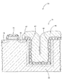
図1は、半導体基板12上の典型的なスタック型キャパシタに組み込んでいるメモリーセル10を例示している。例示されたキャパシタデザインは該産業で、“スタッド(stud)”キャパシタとして知られている。トランジスタが最初に形成され、基板12上に形成されたゲートスタック14、及び基板12中に多量にドープされた活性領域16を含む。コンタクト18は、トランジスタ上にある絶縁層20を通って伸びている。このコンタクト18は、キャパシタ11の、絶縁層20上に形成される下部(lower)または記憶電極22を電気的に接続している。そのスタッド形は、下部(lower)電極22が上に形成される基板のフットプリントに比べ、下部電極22のためのより広い表面積を与えている。薄いキャパシタ誘電体層24は下部またはボトム電極22をコートし、より上のまたは上部電極26はキャパシタ誘電体24上に形成される。
【0006】
図2は、例えば、異なるスタック型キャパシタデザインを有するメモリーセル10aを例示し、ここで類似の部分は類似の参照数字により参照される。図2中のように、キャパシタ11aは基板12上に示されており、絶縁層20で覆われたトランジスターを含む。しかしながら、キャパシタ11aは一般に円筒形に適合する。特に、コンタクト18によって、下にあるトランジスターに電気的に接続する、下部またはボトム電極22aは、円筒形に合い、それが上に形成される基板のフットプリントに比べ、より広い表面積を与えている。示されているように、露出した内側及び外側両方の表面で、ボトム電極22aは、図1中のスタッドキャパシタ11の対応するボトム電極22より、いっそう広い有効表面積を有する。薄いキャパシタ誘電体層24aはボトム電極22aをコートし、上部電極26aはキャパシタ誘電体24a上に形成される。“クラウン(crown)”構造は、例示されている図2の円筒形キャパシタ11aに似ているが、さらに複数の同心円筒を含む。他のスタック型キャパシタデザインはマッシュルームの形、ひれを持った構造、ピン及び半導体基板の上に形成される様々な他の複雑な構造に似ている。
【0007】
図3は、図1及び図2のスタック型キャパシタと対照的に、大部分は半導体基板32内に形成された、典型的なトレンチキャパシタ31を組み込んだメモリーセル30を例示している。以前の図のスタック型キャパシタと同様に、トランジスターは基板32上のゲートスタック34、及び基板32内の多量にドープされた活性領域36を含む。ドレイン領域(活性領域36の1つ)は、キャパシタ31の下部または記憶電極42に電気的に接続されている。ドーピング、又は他の半導体基板32中のトレンチの壁を導電性にすることが、この下部電極42を形成する。トレンチの壁に適合することで、それが中に形成される基板32のフットプリントに比べて、より広い表面積がより低い電極42に提供される。薄いキャパシタ誘電体層44はボトム電極42をコートし、上部または照合電極46はキャパシタ誘電体44上に形成される。
【0008】
しかしながら、メモリーセルの静電容量を増加させるためのその様な構造だけに頼ることは、メモリーチップ集積デザインの進歩的な生成で、非実用的となる。スタッドキャパシタの表面積は、理論上、単にボトム電極の高さを増すことによって無限に増加されることができる。同様に、トレンチキャパシタの深さは、ほぼ、それが中で形成される基板の厚さまで増加されることができる。運悪く、集積回路における形の高さ又は深さには制限がある。該技術で公知のように、従来の堆積技術を使用する高度なステップで、適合するように形をコートし、皺をつけ又は塗り込むことは困難であり得る。さらに、チップ上の増加したトポグラフィーは後のフォトリソグラフィープロセスの分解能に悪影響し得る。
【0009】
それゆえ、セルキャパシタの高さ又は深さだけに頼るよりむしろ、テクスチャ加工された表面又は粗表面を下部電極のマクロ構造折り畳み(fold)に提供することで、キャパシタ電極の表面積をさらに増加させるために、マイクロ構造が加えられ得る。例えばHanらに発行された、U. S. Patent No. 3,405,801で開示されているように、多結晶導電性材料は、例えば、好ましくは粒界に沿ってエッチングすることで、粗面にすることができる。もう1つの方法として、Hirotaらに発行されたU. S. Patent No. 5,372,962は、ポリシリコン層に穴をあけるための様々な選択的エッチプロセスを記載している。
【0010】
電極テクスチャリング技術のもう1つの種類は、半球状粒子(HSG)シリコンの形成に関する。堆積したポリシリコンは選択的に核形成部位上に成長する直接堆積、及び、熱エネルギーがシリコン原子を表面あたりで移動させ、核形成部位あたりで団塊状に凝集させる、アモルファスシリコンの再分配アニール化を含む、HSGシリコンを形成するためのいくつかの方法が知られている。図1及び図2は、基礎スタッドつまり円筒形配置上に形成されたHSGシリコンマイクロ構造28、28aを含む、下部電極22、22aを示し、それによって有効な電極表面積を増加させている。同様に、図3のボトム電極42は、さらに電極表面積を増加させる、基礎トレンチ配置上のHSGシリコン層48を含む。
【0011】
テクスチャ加工されたボトム電極の増加した表面積の利点を完全に実現するために、キャパシタ誘電体層はボトム電極の表面に密に適合すべきである。誘電体厚さ(上述の静電容量式の“d”)は、静電容量を最大にするために、最小にされるべきである一方、あまりにも薄いキャパシタ誘電体は、キャパシタ電極の両端の漏電電流のリスクがある。漏電電流は誘電体中のピンホール、及び量子トンネル効果(quantum tunneling effect)の結果として起こり得、その現象両方とも、より薄い誘電体でより起こりやすい。薄いキャパシタ誘電体層はこのように低い絶縁破壊電圧により特徴付けられ、絶縁破壊漏電が起こる前にボトム電極上に蓄えられ得る電荷を制限する。従って、キャパシタ誘電体層は、選択される誘電体材料に依存した、絶縁破壊を避けるために必要なある最小限の厚さによって特徴付けられ得る。
【0012】
図4を参照して、HSGシリコン層50の拡大図が描かれている。層50は、導電性基板54上の、導電的にドープされた多結晶シリコン(ポリシリコン、又は単にポリ)の半球状粒子52を含む。粒子52は約50Å〜約750Åの範囲の粒子サイズを有する。CVDにより堆積された誘電体層56は、HSG層50上に示されている。図示された誘電体は、酸化ケイ素(SiO2)及び/又は窒化ケイ素(Si3N4)のような従来の誘電体材料を含み、それらはよく理解されており、容易に従来の加工プロセスフローに組み込まれる。例えば、これらの材料のCVDプロセスは、よく開発されている。
【0013】
示されているように、CVDによって堆積された誘電体層56は、HSGシリコン層50の表面上に比較的適合している。しかしながら、従来のCVDプロセスは、様々な要因のため、HSGシリコンのような高い表面積テクスチャ上に、完全に適合した誘電体を製造することはできない。CVDは本来、加工物のトポグラフィーの異なるポイントにおいて、異なる速度で堆積する結果となる。加工物中、特に300-mmウェーハのような大きな加工物中の温度の不均一性は、CVD層の厚さ均一性に強く影響することができる。リアクターデザイン、ガスフロー力学及び枯渇効果(depletion effect)による反応物濃度におけるバリエーションは、同様に、大きい加工物中の厚さの均一性に影響する。これら及び他の問題により、成長速度及び適合は、従来のCVDを使用して、きっちりと正確にコントロールされることはできない。
【0014】
加工物にわたるバリエーションに依存せず、不均一性はまた結果として、でこぼこの表面上のマイクロレベルになる。特に、互いに接近し又は交差する隣接粒子52間のネック領域60で、誘電体層は隣接する粒子52を橋架けし、粒子の上面61上より、より大きい誘電体厚さを効率良く作り出す。いくつかの場合において、凹角の側面62が、開花している又はマッシュルーム形の粒子52間にできる。そのような構造のネック領域60上の誘電体のCVDは、誘電体がピンチオフする間、粒子52間のネック領域を完全に満たすか、又は粒子52間の空洞64を残すかのどちらかである。どちらの場合も、上部電極は粒子52の表面に適合することはできず、その結果、粒子52のより低い部分は事実上失われ、静電容量に貢献しない。
【0015】
もし誘電体56が、HSGシリコン粒子間のネック領域60に最小限の厚さに堆積されるなら、トップ表面上の誘電体はあまりにも薄く、漏電及びその結果としてのデータエラーにつながり得る。従って、誘電体56は、粒子52の上面61上の漏電を避けるために必要とされる最小限の厚さに堆積されなければならない。粒子52のネック領域60にある誘電体56は、この様に、静電容量の減少につながる理論的に必要なのよりも厚い。もう1つの観点から、ネック領域60に渡る誘電体橋架け(bridging)は、HSG粒子52のより低い部分からの表面積の事実上のロスになり、その結果、HSGシリコンの完全な利点は実現されていない。
【0016】
部分的に、電極表面積増加により高められる静電容量におけるそのような制限により、より最近の注目は、その代わりに、キャパシタ誘電体の誘電率(k)を増加させる方法に焦点が当てられている。多くの努力が、より高いk値を有する新しい誘電体材料を組み込む事に向けられている。高k材料は酸化アルミニウム(Al2O3)、酸化タンタル(Ta2O5)、バリウムストロンチウムチタネート(BST)、ストロンチウムチタネート(ST)、バリウムチタネート(BT)、鉛ジルコニウムチタネート(PZT)、及びストロンチウムビスマスタンタレート(SBT)を含む。これらの材料は、従来の誘電体(例えば、酸化及び窒化ケイ素)よりもかなり高い、効果的な誘電率により特徴付けられる。二酸化ケイ素に対してkは3.9である一方、これらの新しい材料の誘電率はおよそ10(酸化アルミニウム)から300(BST)を範囲にとることができ、いくつかはさらに高い(600〜800)。そのような材料を使用することで、セル静電容量/フットプリントをずっと大きく増加させることができる。
【0017】
さらに、キャパシタ誘電体のk値を劇的に増加させると、所定の記憶電荷要件のための、より小さい及びより単純なキャパシタデザインを使用することができる。セルキャパシタの表面積を減らすニーズは、将来の回路デザインに対して、集積プロセスを単純化し、より大きいパッキング密度を可能にできる。
【0018】
しかしながら、高k材料を従来のプロセスフローに組み込むことは、困難であることが分かっている。Ta2O5、BST及び他の“変わった”材料のようないくつかの材料は、非常に酸化性、高温堆積及び堆積後アニール化条件に関係する傾向があり、伝統的な電極材料の酸化、及び、より低い回路素子への酸素の拡散さえも起こってしまう。ZrO2及びTiO2のような他の材料は、プロセス条件の多様性に依存した、非常に一貫性のない特性を有する。
【0019】
従って、組み込まれたメモリーセルの記憶静電容量を増加させる、より効果的な方法への需要がある。
【0020】
【課題を解決するための手段】
発明の要約
この必要性を満たすため、本明細書では、テクスチャ加工されたボトム電極表面上に誘電体および上部電極材料を堆積する方法が提供される。有利には、該方法は、高いコンフォーマリティ(conformality)を達成し、その結果、ライニング層に必要な最小要求厚が全表面上で形成されることを必要とする。該方法は、シリコン電極を維持するのに好ましい条件下で、半球状粒子(HSG)シリコン上に高い誘電率(高k)材料の堆積を可能にする。
【0021】
一般に、該方法は、反応物フェーズを交互に行なうサイクルを含み、そこでは、各フェーズは、自己制限的(self-limiting)効果を有する。約10超の誘電率を有する金属酸化物および三元材料が、リガンド交換反応により、自己終結式金属またはシリコン複合体単層を交互に吸着することによって、形成され得る。吸着された金属またはシリコン複合体上に存在するリガンドは、続いて、酸素含有種の存在によって除去され、ハロゲン化物または有機単層の代わりにOH基および酸素架橋を残す。本明細書では、単純な二元金属酸化物、金属シリケートのような三元材料および異なる組成の交互の超薄型誘電体層を交互に含むナノラミネートに関する例を示す。
【0022】
有利には、該方法は、HSGシリコン上に均一に厚い誘電体層を、望ましくは、そのように形成されるキャパシタ誘電体による漏れ電流を誘発することなく、できるだけ薄く形成することを可能にする。さらに、該方法は、高k材料と高い表面積のテクスチャ加工された電極の組合せを容易にする。こうして、静電容量は最大にされ、セル信頼度の損失なしに、臨界次元の更なるスケーリングを容易にする。
【0023】
類似の交互成分は、好ましくは、コンフォーマルな(conformal)誘電体層上に上部電極材料を形成するために使用される。本明細書には、金属窒化物バリヤーならびに元素金属層の例が示される。好ましい方法による薄いコンフォーマルな導電層の形成に続いて、減少したコンフォーマリティを有する慣用されている堆積が、静電容量を犠牲にすることなく、上部電極の所望の厚さを完全にし得る。好ましい方法により形成されたコンフォーマルなキャパシタ誘電体および上部電極は、こうして、テクスチャ加工されたボトム電極によって生じる増大した表面積の利点を十分に利用可能にする。
【0024】
【発明の実施の形態】
特定の好ましい材料に関連して記載するけれども、本明細書の開示に照らして記載された方法および構造は、凹凸表面上のキャパシタ誘電体に関して好適な様々な他の材料に適用されることが理解される。さらに、メモリーセル記憶キャパシタ(memory cell storage capacitors)に関して例示すると同時に、当業者は、電気的消去書込み可能な読み出し専用メモリー(EEPROM)デバイスのフローティングゲート電極のような他の粗面電極への、記載された方法の適用が容易に認識される。
【0025】
先の従来の技術の項で議論されたように、慣用されている化学気相成長法(CVD)によるキャパシタ電極、および詳しくは半球状粒子(HSG)シリコンを有する電極構造物のコーティングは、完全に満たないコンフォーマリティを生み出す。多くの研究が、一般に半導体のステップ特徴のよりコンフォーマルなステップカバレージ(step coverage)を獲得することに寄与してきたが、同じ濃度の堆積種をそのような構造の全表面に供給するのは非常に困難である。特に、粒子間のネック領域に供給されるように、HSG粒子の上面で、同じ濃度の堆積種を供給するのは困難である。この問題は、テクスチャ加工された電極が図1〜3のスタック型およびトレンチ型デザインのような三次元折り畳み構造に適合する場合に特に悪化し、図2のもののような内部容積を有する構造ではさらに悪化する。従って、HSGシリコンの増大した表面積の充分な利点は、実現されない。
【0026】
殆ど完全なステップカバレージを提供することによって、好ましい実施態様は、HSG粒子の全表面にわたり所望のキャパシタ誘電体層のための最小必要厚を有利に得る。望ましくは、好ましい実施態様の方法は、制限された粒子インターセクションと比較して、粒子上の反応物種の相対的濃度に余り依存しない。
【0027】
さらに、好ましい実施態様は、高い表面積のテクスチャ加工表面及びシリコン電極の集積を可能にするように、高k材料の堆積方法を提供し、それはHSG形態のようなミクロ構造的粗面を生じるのに最もしばしば使用される。三次元折り畳み構造上の高い表面積テクスチャと、高k誘電体との間の選択を提示するよりもむしろ、好ましい実施態様は、反復可能な生産価値の高い方法において、非常に高い静電容量/フットプリントを達成するために、両方の技術を使用可能にする。
【0028】
好ましい実施態様は、Al2O3(k〜10)、ZrO2(k〜12-20)、TiO2(k〜20-50)、混合ジルコニウムシリコンオキサイド(k〜8-13)、および上記の組合せにより形成されるナノラミネート誘電体を堆積するための例示的方法を提供する。同様に、誘電体およびHSGシリコン上に電極材料を堆積する方法が提供される。これらの材料は、HSGシリコンに適合する方法によって全て形成され、さらに殆ど完全なコンフォーマリティを生じる。従って、好ましい実施態様は、高k誘電体材料によるのみでなく、HSGシリコンによって生じる増大した表面積の十分な活用によっても、増大した静電容量を可能にする。そのようなコンフォーマリティは、スタック型およびトレンチ型キャパシタデザインのような、高アスペクト比構造上でさえ獲得する。
【0029】
好ましい方法の更なる利点は、以下の考察から明らかになる。
【0030】
コンフォーマルなキャパシタ誘電体を形成する方法
図5は、一般に、高いステップカバレージを有するキャパシタ誘電体層を形成する方法を例示する。好ましい方法は、原子層堆積(atomic layer deposition: ALD)の形態であり、それによって、反応物は、サイクル中のパルス交換において加工品に供給される。好ましくは、各サイクルは、吸着によって、より好ましくは化学吸着によって、材料の約1以下の単層を形成する。基板温度は、化学吸着を促進するウィンドウ内に維持される。特に、基板温度は、吸着複合体とその下層表面との間の無傷の結合を維持するのに、および前駆体の分解を防止するのに、充分に低い温度で維持される。他方、基板温度は、反応物の縮合を回避し、各フェーズ中の所望の表面反応のための活性化エネルギーを提供するために、充分に高いレベルに維持される。勿論、任意の所与のALD反応に関する好適な温度ウィンドウは、関与する表面末端および反応物種に依存する。
【0031】
各サイクルの各パルスまたはフェーズは、好ましくは、効果において自己制限的である。下記の例において、フェーズのそれぞれは、自己終結式(self-terminated)である(即ち、吸着された及び好ましくは化学吸着された単層は、そのフェーズの成分と非反応性の表面と共に残される)。過剰の反応物前駆体が、構造表面を飽和するために、それぞれのフェーズで供給される。表面飽和は、全ての利用可能な反応部位(下記でより詳細に議論されるように、物理的サイズ制限に従う)を反応物で占めることを確実にするが、自己終結は、反応物へのより長い暴露に供された位置では、過剰なフィルム成長を妨げる。化学吸着による飽和の全体的活用、即ち、自己終結式成分は、優れたステップカバレージを確実にする。
【0032】
誘電体層を形成する前に、キャパシタを下部またはボトム電極に構築する点に、先ず集積回路を部分的に加工する。代表的には、ボトム電極は、メモリーセル中の記憶電極(storage electrode)として機能する。しかしながら、本説明の目的のために、ボトム電極は、それが完全な集積回路中の記憶(storage)またはリファレンス(reference)プレートとして機能するかどうかに関わらず、最初に形成されたキャパシタ電極またはプレートを示す。
【0033】
図5に示されるように、好ましい二元材料の実施態様に従う方法は、集積回路中におけるボトム電極構造の形成100で始まる。基本的なボトム電極構造は、EEPROMデバイス中でフローティングゲートのような平面であり得る。しかしながら、好ましくはボトム電極は、メモリーセルで占められる基板フットプリントよりも大きい表面積を有する三次元折り畳み構造に適合する。より好ましくは、キャパシタボトム電極は、図1に例示されるスタッド型コンフィギュレーションまたは図2に例示される円筒型コンフィギュレーションのようなスタック型キャパシタの形態を採る。当業者は、本明細書に開示される方法が、王冠、ひれ付構造、櫛、ピンなどのような他のスタック型キャパシタデザインにも適用されることを容易に認識する。他のアレンジメントでは、キャパシタボトム電極は、図3に例示されるように、半導体基板内に形成されるトレンチの壁を、導電性にドープする及び/又は導電性にライニング(lining)することによって形成される。
【0034】
ボトム電極マクロ構造の形成後、スタック型またはトレンチ型アレンジメントのいずれかにおいて、ボトム電極は、続いて、三次元折り畳み形状上に重ねられたテクスチャ加工または粗面ミクロ構造を設けられ101、好ましくはHSGシリコンの層の形態でボトム電極の表面積をさらに増強する。
【0035】
ASM, International, Inc.の商品名A600 UHVTMで販売されているバッチシステム中で行なわれる例示的加工では、アモルファスシリコン堆積、シーディング(seeding)および再分布アニールによってHSGシリコンが形成される。三次元折り畳み構造が、アモルファスシリコンで形成されるか又はコートされる。幾つかの方法では、アモルファスシリコン堆積は、例示される実施態様では、in situで同じ反応チャンバー内で後続の工程のように行なわれ得るけれども、折り畳みアモルファスシリコン構造は、A600 UHVTMシステムにウェーハを移送する前に、形成される。
【0036】
好ましい反応器内で、アモルファスシリコン表面がシードされる。例示される実施態様では、温度を、約550℃〜575℃(例えば、約560℃)の範囲内のレベルに上昇させるが、反応器圧力を、好ましくは約10−5Torrのオーダーに減少する。好ましい実施態様でのシーディングガスは、約4×10⁻⁶Torrのシラン分圧で供給される、モノシランである。シーディング後、その密度がデザインにより変化し得、所望の温度での持続的熱処理は、可動性アモルファスシリコンの再分布をもたらす。ケイ素原子は、シランにより形成されたシードまたは核形成部位の周囲に凝集する傾向がある。方法全体は、温度ランプ、シーディングおよびアニールを含むバッチシステムに関しては、約10分および120分のオーダーで起こる。当業者は、HSGシリコンを形成するための多くの他の技術を容易に認識する。
【0037】
好ましい方法で作製されたHSG粒子は、約50Å〜750Åのサイズ、より代表的には約300Å〜500Åの範囲であり得る。核形成密度およびHSGシリコン粒子サイズに影響するプロセス条件は、代表的には、互いに大きく離れた粒子を残すように選択される。そのようなアレンジメントは、後続の誘電体および上部電極層の殆どを粒子間にフィットさせる制限内で、電極表面積を最大にする。しかしながら、図9〜12の拡大図から認識されるように、粒子は、固有のランダムシーディングプロセスにより、幾つかの位置でランダムに集中する。さらに、好ましい誘電体および上部電極層は、より密で、より離れていない粒子の使用を可能にし、こうして使用可能な表面積を増加させる。
【0038】
当業者に認識されるように、ボトム電極は、好ましくは、ダイナミックランダムアクセスメモリー(DRAM)アレー中で、メモリーセルの記憶ノード(storage node)として機能する。加工後、ボトム電極は代表的には、図1A、1Bおよび2に示されるように、アレーを横切って他のセルのボトム電極から隔離される。
【0039】
そのように形成されたボトム電極構造は、その後、高いステップカバレージでコートされる。好ましい実施態様に従うと、誘電体層は、周期的方法で形成され、そこでは、各サイクルは、自己制限的様式で加工品上に、約1以下の単層の誘電体材料を形成する。好ましくは、各サイクルは、少なくとも2つの異なるフェーズを含み、そこでは、各フェーズは、飽和反応、即ち、所望の誘電体材料の約1以下の原子単層を自己制限的に残す。
【0040】
必要なら、ボトム電極(例えば、好ましい実施態様のHSGシリコン)の露出された表面は、終結して102、ALD方法の第1フェーズと反応する。好ましい金属酸化物の実施態様(表I〜Vを参照)の第1フェーズは、例えば、ヒドロキシル(OH)またはアンモニア(NH3)終結部(termination)と反応性である。下記の実施例では、HSGシリコンのシリコン表面は、一般に、別の終結部を要求しない。清浄な室内環境にさらされると、自然にOH終結部102を提供する天然の酸化物形成を生じる。HSGがin situで又は誘電体形成前にクラスターツールで形成される場合、HSGを、例えば、表面調製または終結部102処理としてH 2O蒸気にさらすことが望ましいかもしれない。他のアレンジメント(下記の表IIおよびIIIの考察ならびに図10を参照)では、金属酸化物は、別の終結工程なしに、窒化ケイ素上に直接形成もされ得る。換言すれば、HSGシリコンの窒化は、終結部102として機能し得る。
【0041】
最初の表面終結部102後、必要ならば、第1成分は、続いて、加工品に供給される104。図7を参照して下記でより詳細に議論されるように、好ましい金属酸化物の実施態様に従うと、第1成分は、先の工程102によって残された終結表面と反応性である金属含有化合物を含む。従って、金属複合体は、リガンド交換により、表面終結部と交換する。得られた金属含有単層は、望ましくは自己終結的であり、その結果、第1成分の任意の過剰な構成要素は、この方法で形成された単層と更に反応することはない。好ましくは、ハロゲン化物または有機リガンドは、金属含有単層を終結させる。
【0042】
金属含有反応性種は、好ましくは、ガス状形態で供給され、従って、以下で金属源ガスと称される。第1成分は、続いて、反応チャンバーから除去される106。例示される実施態様では、工程106は、キャリアガスを充分な時間流し続けながら、単に第1成分の流動を停止させることを必要とし、好ましくは反応チャンバー体積の約2倍以上、より好ましくは、チャンバー体積の約3倍以上のパージガスを用いて反応チャンバーから過剰な反応物および反応物副生成物を拡散しまたはパージする。例示される実施態様では、除去106は、第1成分の流動を停止後、約0.1秒〜20秒の間、パージガスの流動を持続させることを包含する。パルス内パージは、1999年9月8日に出願されたSerial No.09/392,371の、IMPROVED APPARATUS AND METHOD FOR GROWTH OF A THIN FILMという発明の名称を有する、同時係属中の米国特許出願に記載され、その開示は本明細書中に参考として援用される。他のアレンジメントでは、チャンバーは、成分を交換する間に、完全に排気され得る。例えば、1996年6月6日に公開されたPCT国際公開WO96/17107の、METHOD AND APPARATUS FOR GROWING THIN FILMSという発明の名称を有する出願を参照のこと、その開示は本明細書中に参考として援用される。同時に、過剰の反応物および副生成物の吸着104および除去106は、ALDサイクル中で第1フェーズを示す。
【0043】
第1成分の未反応(または過剰の)反応物がチャンバーから除去106されたとき、第2成分は加工品に供給108される。第2成分は、望ましくは、工程104で形成される自己終結式単層と反応する。図7を参照して下記でより詳細に説明される、例示される金属酸化物の実施態様では、この反応は、酸素源ガスを加工品(workpiece)に供給することを包含する。酸素源ガスからの酸素または酸素含有複合体は、好ましくは、先に吸着された金属複合体上で反応し、金属複合体単層の代わりに、金属酸化物単層を残す。
【0044】
他のアレンジメントでは、第2成分は、工程104で形成された、吸着された金属複合体単層のリガンド終結を単純に除去し(例えば、昇華または還元による)、或いは、更なる成分の酸化または化学吸着のための単層を調製し得る。
【0045】
望ましくは、反応108も、自己制限的である。反応物は、工程104で残された制限された数の反応部位を飽和する。温度および圧力条件は、好ましくは、単層から下層の材料までの第2成分からの反応物の拡散を回避するようにアレンジされる。第2成分は、第2成分中で過剰な反応物と反応性でない表面終結部も残し、こうして、飽和反応フェーズにおける堆積を制限するように作動する。下記の表I〜Vの例示された実施態様では、金属酸化物単層上のヒドロキシル(OH)テイル(tail)および酸素架橋終結部は、第2成分の過剰な酸素源ガスと非反応性である。
【0046】
第2成分の化学吸着(または自己制限的反応)により金属複合体単層の表面を完全に飽和するのに充分な時間後、過剰な第2成分は、加工品から除去される110。第1成分の除去106の場合と同様に、この工程110は、好ましくは、第2成分の流動を終結すること、および第2成分の過剰な反応物および反応副産物を反応チャンバーからパージするのに充分な時間、キャリアガスの流動を持続させることを包含する。例えば、反応物および反応副産物は、好ましくはパージガスの少なくとも約2倍のチャンバー体積を用いて、より好ましくは、少なくとも約3倍のチャンバー体積を用いて、第1成分の流動を停止した後、パージガスを流動させることによって除去され得る。例示される実施態様では、除去110は、第1成分の流動を停止後、約0.1秒〜20秒間、パージガスの流動を持続させることを包含する。同時に、反応108および除去110は、ALDサイクル中の第2フェーズ111を示す。
【0047】
例示される実施態様では、一旦、第2成分の過剰な反応物および副産物が反応チャンバーからパージされたら、ALDプロセスの第1フェーズが繰返されるように2つのフェーズが交代する。従って、再び加工品への第1成分の供給104は、他の自己終結式単層を形成する。
【0048】
2つのフェーズ107、111は、従って、ALDプロセス中で単層を形成するために繰返されるサイクル115を示す。第1成分は、一般に、先のサイクル中の第2成分によって残された終結部と反応(リガンド交換において)または化学吸着する。必要なら、サイクル115は、図5,6中の点線で示されるように、工程102に類似する異なる表面調製を含むように、拡大され得る。サイクル115は、次に、工程104〜110を続ける。このサイクル115は、回路作動の間、電流漏れを回避するのに充分な厚さのHSGシリコン上の誘電体層を作製するだけの充分な回数、繰返される。或いは、より薄い層の後には、下記の図11の考察からよりよく理解されるように、誘電体下層(dielectric sublayer)のスタックを形成するために、類似のALDプロセスによって堆積された更なる誘電体層が従い得る。
【0049】
図6を参照して、更なる成分も、各サイクル中に含まれ得る。図6では、図5のものに対応する工程は、図5の100シリーズよりも、200シリーズ中の同じ最後の2桁を有する数で参照される。従って、工程200−210は、図5の対応する工程100−110と類似している。
【0050】
しかしながら、図6の例示されるサイクル215は、2つの更なるフェーズを含むように拡大する。第1フェーズ207および第2フェーズ211は、自己終結式金属酸化物またはシリコン酸化物単層を形成する。第3フェーズ219および第4フェーズ223は、別の自己終結式金属酸化物またはシリコン酸化物単層を形成する。第2単層の組成は、好ましくは、レシピデザイナーの裁量により、第1単層の組成と異なる。例えば、下記の表VIの金属ケイ酸塩の例を参照。
【0051】
特に、第1金属/シリコンフェーズ207および第1酸素フェーズ211が第1金属酸化物またはシリコン酸化物単層を形成した後、第2金属またはシリコン源ガスが供給され216、先に形成された金属/シリコン酸化物上に、自己制限的(self-limiting)もしくは自己終結式(self-terminating)金属またはシリコン複合体単層を形成する。第1金属/シリコンフェーズ207と同様に、金属/シリコンガス源は、先に形成された金属/シリコン酸化物上で、リガンド交換(化学吸着)によって反応し得る。反応物の別の除去(排気または好ましくはパージによる)218の後、第2酸素ガス源が供給され220、続いて、除去される222。第2酸素工程220(または酸素フェーズ223)も、自己制限的である。第1酸素工程208の場合のように、酸素ガス源は、リガンド交換(化学吸着)によって反応し得る。
【0052】
例示される方法は、各サイクル215中の4フェーズを含むけれども、サイクル215は、それが三元誘電体を生じるので、本明細書中で「三元サイクル215」と称される。これは、第2フェーズ211および第4フェーズ223が共に、成長する誘電体層に同じ元素(酸素)を寄与するという事実による。他のアレンジメントでは、誘電体層中の所望の酸素含量に依存して、第2フェーズまたは第4フェーズのいずれかが省かれ得ることに注目。そのような場合、連続的成分は、充分小さいリガンドで表面終結をもたらし、後続の成分の或る拡散を可能にするために、および/または省かれた酸素フェーズの代わりに中間リダクションフェーズ(intermediate reduction phase) を有するために、リガンド交換反応を生じさせるように選択されるであろう。
【0053】
第3フェーズ219における第2金属/シリコン源ガスは、第2金属/シリコン源ガスと非反応性であるハロゲン化物または有機リガンドで自己終結式である金属複合体単層を生じる、金属ハロゲン化物または金属有機前駆体であり得る。しかしながら、表VIの例の中では、第2金属/シリコン源ガスは、自己制限的化学吸着に伝導性のシリコン源ガス、例えば、3-アミノプロピルトリエトキシシラン(NH2CH2CH2CH2-Si(O-CH2CH3) 3またはAMTES)あるいは3-アミノプロピルトリメトキシシラン(NH2CH2CH2CH2-Si(O-CH3)3またはAMTMS)化合物、或いはハロシランを含む。金属源およびシリコン源フェーズの順序は、逆にされ得ることに注目。
【0054】
第4フェーズ220の酸素源ガスは、第2フェーズ211のものと同じでも異なっていても良い。本発明者は、有機リガンドを有する金属またはシリコン複合体単層を酸化するのに有利である特定のオキシダント(例えば、オゾン)を見い出したが、他のオキシダント(例えば、水)は、ハロゲン化物終結式金属またはシリコン複合体単層にとってより有利である。従って、下記の表VIの例中では、第4フェーズ223のオキシダントは、第3フェーズ219のオキシダントとは、少なくともそれらのサイクルに関して異なり、そこでは、第3フェーズ219の金属/シリコン源は、第1フェーズ207の金属/シリコン源と異なる。
【0055】
得られる誘電体中の異なる金属または金属:シリコンのおおよそ1対1比率のために、示されるように、サイクル215を繰返す。下記の表VIの例中では、例えば、金属、酸素、シリコンおよび酸素フェーズによる繰返しサイクルは、この順序では、金属ケイ酸塩層を生じる。或いは、三元誘電体に関して例示されるサイクル215は、一連の二元サイクル115(図5)の後に、得られた三元誘電体中の異なる金属の所望の比率に依存して、行なわれ得る。逆に、二元サイクル115(図5)は、一連の三元サイクル215の後に、行なわれ得る。ガスフローバルブをコントロールするソフトウェアは、例えば、全ての3つの二元サイクル115後に1つの三元サイクル215を行なうように、プログラムされ得る(図5)。そのような方法は、誘電体層中の第1金属対第2金属(またはシリコン)のおおよそ3:1比を生じるであろう。当業者は、本明細書中の開示に照らして、第2金属がプロセス中で置換される頻度に、および化学吸着された分子の相対的物理的サイズに、実際の比率が依存することを認識する。
【0056】
二元および三元方法の両方とも、下記の実施例中で当初の金属/シリコンフェーズおよび後続の酸素フェーズにより、図5および6で例示されるけれども、サイクルは、より低い表面およびフェーズ成分に依存して、酸素フェーズで始まり得ることが理解される。
【0057】
【実施例】
金属酸化物誘電体を形成する方法
下記の図7及び表I〜Vは、ボトム電極のHSGシリコン上の金属酸化物誘電体を形成するための例示的プロセスを説明している。表Iは非遷移金属(例えば、アルミニウム)の酸化物の形成を例示している;表II及びIIIはV族遷移金属(例えば、バナジウム、ニオビウム、タンタル)の酸化物形成を例示している;表IV及びVはIV族遷移金属(例えば、チタン、ジルコニウム、ハフニウム)の酸化物形成を例示している。単純化のため、類似の参照数字が、図5の一般記載に対応する、金属酸化物例のフェーズ及びステップ(図7)を参照するために使われている。
【0058】
図7を参照すると、ガスフロー手順は特別な実施例と一致して表される。説明された実施例において、高k誘電体、及びより詳細には高k金属酸化物は、製造工程にある製品(workpiece)に金属源ガスを、酸素源ガスと交互に供給することにより形成される。それぞれのサイクルの第一のまたは金属フェーズ107は、望ましくは酸素源ガスなしで、金属含有材料の層を化学吸着する。それぞれのサイクルの第二のまたは酸素フェーズ111は、望ましくは金属源ガスなしで、堆積された金属含有層上の酸素含有材料と反応又は吸着する。他のアレンジメントにおいて、フェーズの順番は逆にされることができ、反応物の除去またはパージ工程は前の又は後の反応物パルスの一部であると考えられ得ることは、理解されるだろう。
【0059】
誘電体材料がその上で形成される表面は、金属源ガスと反応する表面を提供するために、最初に終結(terminate)される。好ましい実施態様において、その上で堆積が望まれる露出した表面は、OH末端(図9参照)及び窒化ケイ素(図10)参照)を有するHSGシリコンを含む。
【0060】
最も好ましくは、金属フェーズ107は自己制御式であるので、その結果第一フェーズの間、約1以上の原子単層は堆積されない。望ましくは、揮発性金属源ガスはパルス104中に提供される。例示的な金属源ガスは:トリメチルアルミニウム(TMAまたは(CH3)3Al);アルミニウムクロライド(AlCl3);アルミニウムベータジケトネート(例えば、Al(acac)3);タンタルエトキシド(Ta(OCH2CH3)5);タンタルペンタクロライド(TaCl5);ペンタキス(ジメチルアミノ)タンタル(Ta [N(CH3)2]5);ジルコニウムテトラクロライド(ZrCl4);ジルコニウムブトキシド(Zr(OCH2CH2CH2CH3)4);チタンテトラクロライド(TiCl4);チタンイソプロポキシド(Ti[OCH(CH3)2]4);テトラキス(ジメチルアミノ)チタン(Ti[N(CH3)2]4);テトラキス(ジエチルアミノ)チタン(Ti[N(C2H5)2]4);タングステンヘキサフルオライド(WF6);3-アミノプロピルトリエトキシシラン(NH2CH2CH2CH2-Si(O-CH2CH3)3つまりAMTES);3-アミノプロピルトリメトキシシラン(NH2CH2CH2CH2-Si(O-CH3)3つまりAMTMS);ジクロロシラン(DCS);トリクロロシラン(TCS);バナジウムトリクロライド(VCl3);バナジウムアセチルアセトネート(V(acac)3);ニオビウムペンタクロライド(NbCl5);ニオビウムエトキシド(Nb(OCH2CH3)5);ハフニウムテトラクロライド(HfCl4)等を含む。
【0061】
金属源ガスがボトム電極の表面を飽和するのに十分な時間が経った後、金属源ガスのフローを止めることが、金属パルス104を止める。好ましくは、金属源ガスがチャンバーから取り除かれるまで、キャリアガスはパージ工程106中、フローし続ける。
【0062】
パルス104の間、金属源ガスは製造工程にある製品の露出した表面と反応し、金属複合体の“単層”を堆積または化学吸着させる。理論的に、反応物は製造工程にある製品の露出した層上のそれぞれの利用できる部位で化学吸着する一方で、吸着された(特に大きい末端リガンドを有する)複合体(complex)の物理的サイズは一般に、それぞれのサイクルでのカバレージ(coverage)を単層の一部に制限するだろう。表Iの例で、ALDプロセスは、およそ1Å/サイクルで金属酸化物層を成長させ、その結果、十分な単層が効果的に、Al2O3に対して約3サイクルおきに堆積された材料から形成し、それは約3Åのバルク格子パラメータ(bulk lattice parameter)を有する。それぞれのサイクルは金属源ガス及び酸素源ガスパルスの対により表される。それゆえ、本明細書で使用されているような“単層”は、堆積の間の単層の一部を表し、主にパルス104の自己制限式効果を示す。
【0063】
特に、製造工程にある製品に提供される金属含有種は自己終結式であり、その結果吸着された複合体表面は、金属源ガスとそれ以上反応しないであろう。以下で述べられる例において、TMA(表I)はメチル終結式アルミニウム(methyl-terminated aluminum)の単層を示す。タンタルエトキシド(表II)はエトキシドタンタルの単層を残す。同様に、他の揮発性金属ハライドはハライド終結式表面(halide-terminated surface)を残し、有機金属前駆体は有機リガンドで終結化(terminated)された表面を残すだろう。その様な表面は、金属源ガスパルス104の間、金属源又は他の反応物フローの成分とそれ以上反応しない。反応物に過剰にさらすことが過剰堆積にならないので、該プロセスの金属フェーズ107の間の成分は飽和的、又は自己制限式(self-limiting)であると言われる。より大きい濃度の反応物への、より長時間の露出にも関わらず、HSGシリコン粒子の上部表面上の堆積は、粒子間のネック領域における堆積を越えない。
【0064】
サイクル115の第二のフェーズ111において、それから、酸素源ガスのパルス108は、製造工程にある製品に提供される。説明された実施例において、酸素源ガスは水蒸気(H2O)又はオゾンを含む。他の好適なオキシダントは:過酸化水素(H2O2);メタノール(CH3OH);エタノール(CH3CH2OH);酸化窒素(N2O、NO2);Oラジカル等を含む。ラジカルは、反応チャンバーにつながっている遠隔プラズマ源により提供されることができ、オゾン発生器は同様にオゾン(O3)を提供することができる。好ましくは、第二フェーズ111は、第一フェーズ107で残った金属複合体の単層を、酸素源ガスに十分にさらすため、十分な時間保持される。酸素源ガスがHSGシリコン層上の金属含有単層を飽和するのに十分な時間がたった後、酸素源ガスのフローを止めることで、酸素パルス108を停止する。好ましくは、キャリアガスは、パージ工程110中、酸素源ガスがチャンバーから取り除かれるまで、フローし続ける。
【0065】
酸素パルス108の間、酸素源ガスは第一フェーズ107により残った、自己終結式の金属複合体単層と反応する、もしくは、その上に化学吸着する。説明された実施例において、この化学吸着は飽和的リガンド交換反応を含み、金属含有単層の有機リガンド又はハライド末端(termination)を、酸素又は酸素複合体で置換する。金属酸化物はそれによって、好ましくは1つの単層中に形成される。望ましくは、該プロセスは、ハイドロキシ及び酸素ブリッジ末端(termination)を有する、化学量論量の金属酸化物を残す。金属フェーズ107に関して述べたように、吸着複合体の物理的サイズのため、単層はすべての利用できる部位を占める必要はない。しかしながら、第二フェーズ111もまた、自己制限式効果を有する。
【0066】
特に、酸素源ガスは、金属源ガスの前のパルスの間、製造工程にある製品の表面上に化学吸着した金属複合体のリガンドと反応する。その反応も表面制限又は終結式である。なぜなら、パルス108間のオキシダントは、金属酸化物単層のヒドロキシル及び酸素ブリッジ末端と反応しないからである。さらに、温度及び圧力の条件は、オキシダントの、金属単層を通って下にある材料への拡散を避けるようにアレンジされる。この飽和的、自己制限式の反応フェーズ111において、反応物のより大きい濃度への、より長時間の露出にも関わらず、HSGシリコン粒子の上部表面上に形成される金属酸化物の厚さは、粒子間のネック領域に形成される金属酸化物の厚さを越えない。
【0067】
(金属源パルス104及びパージ106を含む)金属フェーズ107及び(酸素源パルス108及びパージ110を含む)酸素フェーズ108は一緒に、ALDプロセス中繰り返されるサイクル115を定義する。最初のサイクル115の後、第二のサイクル115aが行われ、ここで金属源ガスパルス104aは再び供給される。金属源ガスは、前のサイクル115中に形成された金属酸化物の表面上で、金属複合体を化学吸着する。金属含有種はすぐに露出した表面と反応し、もう1つの金属複合体の単層又は単層の一部を堆積し、金属源ガスとそれ以上反応しない自己終結式表面を再び残す。金属源ガスフロー104aは止められ、チャンバーから取り除き106a、第二サイクル115aの第二フェーズ111aは、第2の金属単層を酸化するために酸素源ガスを提供する。
【0068】
サイクル115aは少なくとも約10回、より好ましくは少なくとも約20回、メモリーセルオペレーション中の漏電を避けるために、十分に厚い金属酸化物が形成されるまで、繰り返される。有利なことに、約10Å〜200Å、及びより好ましくは約25Å〜100Åの均一な厚さを有する層は、好ましい実施態様の方法により、ほぼ完璧なステップカバレージで、形成されることができる。
【0069】
下記の表は、超大スケールの集積プロセッシングのためのDRAMメモリーセルにおけるキャパシタ誘電体応用に適した、金属酸化物及び三元誘電体層を形成するための模範的なプロセス手法を提供する。誘電体は特にHSGシリコン上の堆積に適している。それぞれのプロセス手法は、単一ウェーハプロセスモジュールにおいて、1つのサイクルを表す。特に、説明されたパラメーターは、フィンランドのASM Microchemistry Ltd.から商業的に入手可能である商品名Pulsar 2000TMの下で、商業的に入手可能である単一ウェーハALDモジュールにおける使用のため開発された。
【0070】
下記の表におけるパラメーターはただ例示的のみであることに注意すること。それぞれのプロセスフェーズは望ましくはボトム電極表面を飽和するためにアレンジメントされている。パージステップは、反応チャンバーから反応性フェーズ間の反応物を取り除くためにアレンジメントされている。説明的なALDプロセスは、約400Åの平均粒子サイズを有するHSG粒子上に、約95%以上の厚さ均一性、及びより好ましくは約98%以上の厚さ均一性を達成する。厚さ均一性は、本明細書で使用されているように、厚さ最大値のパーセントとしての、厚さ最小値のパーセントとして定義されている。本明細書での開示の点から見て、許容の堆積速度で飽和された、自己終結式フェーズを達成するために、当業者はすぐに堆積条件を、異なる反応チャンバー及び異なる選択される条件に修飾し、代用し、又はそうでなければ変えることができる。
【0071】
有利なことに、本明細書で記載されているALDプロセスは、反応物の供給がテクスチャ加工表面を飽和するのに十分である限り、圧力及び反応物濃度に対して比較的敏感でない。さらに、該プロセスは低温で行うことができる。製造工程にある製品の温度は好ましくは、熱的予算を維持する一方で、比較的速い堆積速度を達成するために、該プロセスの間中、約150℃〜350℃に維持される。より好ましくは、該温度は反応物に依存して約220℃〜300℃に維持される。チャンバー内の圧力は、ミリTorr(milliTorr)値域から過圧(super-atmospheric)の範囲をとることができるが、好ましくは約1 Torr〜500 Torr、より好ましくは約1 Torr〜10 Torrで維持される。
【0072】
【表1】

【0073】
第一サイクルの第一フェーズにおいて、TMAはボトム電極のHSGシリコン表面上に化学吸着する。金属源ガスは好ましくは、ボトム電極表面を飽和するために、その他のプロセスパラメーターを与えられた、十分なキャリアフローの割合を含む。アルミニウム複合体の単層はHSGシリコン表面上に残され、この単層はメチル末端で自己終結式である。
【0074】
TMAフローが停止され、続けられたキャリアガスのフローによりパージされた後、H2Oのパルスが製造工程にある製品に供給される。その水は、リガンド交換反応で、金属単層のメチル末端表面とすぐに反応し、酸化アルミニウム(Al2O3)の単層を形成する。該反応は、前もって化学吸着された利用できる金属複合体の数により制限される。さらに該反応は、水もキャリアガスも、結果として生じる酸化アルミニウム単層のヒドロキシル及び酸素ブリッジ末端とそれ以上反応しないという点で、自己制限式である。さらに、好適な温度及び圧力パラメーターは、金属単層にわたる水又は反応副生成物の拡散を抑制する。
【0075】
次のサイクルにおいて、第一フェーズはTMAを導入し、そのTMAはすぐに酸化アルミニウム単層の表面と反応し、一番目の金属酸化物層の上に、再びメチル終結式(methyl-terminated)アルミニウム層を残す。次に、第二サイクルの第二フェーズは、第一サイクルに関して記載されたようなものである。これらのサイクルは酸化アルミニウムの所望の厚さが形成されるまで繰り返される。
【0076】
例示された実施態様において、キャリアガスはそれぞれのサイクルの両方のフェーズの間、一定の速度でフローし続ける。しかしながら、反応物は交互のガスパルス間のチャンバーの排気により取り除くことができることは理解されるであろう。ひとつのアレンジメントにおいて、パルス堆積の間、一定の圧力を維持するために、好ましいリアクターはハードウェア及びソフトウェアを組み込んでいる。Posaへの1988年5月31日発行のU. S. Patent No. 4,747,367、及びCongerらへの1988年8月2日発行のU. S. Patent No. 4,761,269の公開は本明細書に、参考として援用される。
【0077】
プラズマ生成器により提供されるラジカルにより、ALDプロセスの低温で、金属含有層の堆積を容易にすることができる。ラジカル増進での層堆積の構造及び方法は、1999年9月8日提出の、薄膜成長のための改良された装置及び方法(IMPROVED APPARATUS AND METHOD FOR GROWTH OF A THIN FILM)という発明の名称で、Serial No. 09/392,371を有する特許出願で提供されており、その開示は上記で参考として援用される。もう1つの例示的ALDプロセスフローは、1999年6月29日発行の、ShermanへのU. S. Patent No. 5,916,365中に提供されており、その開示は本明細書に参考として援用される。
【0078】
【表2】
【0079】
バリヤー層形成の後、Ta2O5がALDプロセスで形成される。表IIに示したように、説明された金属源ガスはタンタルエトキシド(Ta(OCH2CH3)5) を含む;キャリアガスは窒素(N2)を含む;及び酸素源ガスは好ましくはオゾン(O3)を含む。該プロセス中の温度は、好ましくは約150℃〜300℃、より好ましくは約220℃に保たれる。
【0080】
第一サイクルの第一フェーズにおいて、タンタルエトキシド(tantalum ethoxide)はHSGシリコンの窒化された表面上に化学吸着する。金属源ガスは好ましくは、窒化コートされたHSGシリコン表面を飽和するために、その他のプロセスパラメーターを与えられた、キャリアフローの十分な割合を含む。タンタル複合体の単層はテクスチャ加工表面上に残され、この単層はエトキシド末端で自己終結式である。
【0081】
金属源ガスフローが停止され、キャリアガスの連続的フローにより取り除かれた後、オゾンのパルスが製造工程にある製品に供給される。オゾンは好ましくは、金属含有単層表面を飽和するために、その他のプロセスパラメーターに与えられた、キャリアフローの十分な割合を含む。オゾンは、リガンド交換反応で、金属含有単層のエトキシド終結化表面(ethoxide-terminated surface)とすぐに反応し、酸化タンタル(Ta2O5)の単層を形成する。該反応は、前もって化学吸着された利用できる金属複合体の数によって制限される。オゾンもキャリアガスも、結果として生成した酸化タンタル単層とそれ以上反応しない。オゾンは有機リガンドを燃焼させ、CO2及びH2Oを放出し、該単層はヒドロキシル及び酸素ブリッジ末端をあとに残す。さらに、好適な温度及び圧力パラメーターは、金属単層を通るオゾン及び反応副生成物の拡散を抑制する。
【0082】
次のサイクルにおいて、第一フェーズはタンタルエトキシドを導入し、そのタンタルエトキシドはすぐに酸化タンタル単層の表面と反応し、再びエトキシド終結化タンタル層を残す。次に第二サイクルの第二フェーズは、第一サイクルに関して記載されたようなものである。これらのサイクルは、酸化タンタルの所望の厚さが形成されるまで繰り返される。好ましくは、約40Å〜100ÅのTa2O5を形成するために、約80〜200サイクルが行われる。より好ましくは、約40Å〜50Åを形成するために、約80〜100サイクルが行われる。
【0083】
説明された実施態様において、それぞれのサイクルの両方のフェーズの間、キャリアガスは一定速度でフローし続ける。しかしながら、交互のガスパルス間のチャンバーの排気により、反応物は取り除かれることができることは理解されるであろう。ひとつのアレンジメントにおいて、パルス堆積の間、一定圧力を維持するために、好ましいリアクターはハードウェア及びソフトウェアを組み込んでいる。Posaへの1988年5月31日発行のU. S. Patent No. 4,747,367、及びCongerらへの1988年8月2日発行のU. S. Patent No. 4,761,269の開示は本明細書に参考として援用される。
【0084】
アモルファスTa2O5誘電体層は、ほんの微量の炭素とともに残される。この層は、所望なら、結晶化誘電体に対してアニーリングすることができる。該層の誘電率は約20〜25である。
【0085】
【表3】
【0086】
第一サイクルの第一フェーズにおいて、塩化タンタルはHSGのシリコン窒化表面上に化学吸着する。金属源ガスは好ましくは、窒化コートされたHSGシリコン表面を飽和するために、その他のプロセスパラメーターに与えられた、キャリアフローの十分な割合を含む。タンタル複合体の単層はテクスチャ加工表面上に残され、この単層はクロライド末端で自己終結式である。
【0087】
TaCl5フローが停止され、キャリアガスの連続的フローにより取り除かれた後、水蒸気のパルスが製造工程にある製品(workpiece)に供給される。水蒸気は好ましくは、金属含有単層表面を飽和するために、その他のプロセスパラメーターに与えられた、キャリアフローの十分な割合を含む。水は、リガンド交換反応で、金属含有単層のクロライド終結式表面とすぐに反応し、酸化タンタル(Ta2O5)の単層を形成する。該反応は前もって化学吸着された、利用できる金属クロライド複合体の数によって制限される。水もキャリアガスも、結果として生成した酸化タンタル単層のヒドロキシル及び酸素ブリッジ末端とそれ以上反応しない。さらに、好適な温度及び圧力パラメーターは、金属単層を通る水及び反応副生成物の拡散を抑制する。
【0088】
次のサイクルにおいて、第一フェーズは塩化タンタルを導入し、その塩化タンタルはすぐに酸化タンタル単層の表面と反応し、再びクロライド終結式タンタル層を残す。それから第二サイクルの第二フェーズは、第一サイクルに関して記載されたようなものである。これらのサイクルは、前述の実施例に関して記載されたように、酸化タンタルの所望の厚さが形成されるまで繰り返される。
【0089】
前述のように、パルス間にパージすることが好ましいが、示されたように安定なキャリアガスフローにより取り除かれるよりもむしろ、チャンバーはパルス間に反応物を取り除くために排気されることができる。
【0090】
アモルファスTa2O5誘電体層は、ほんの微量の塩素のみとともに残される。この層は、所望なら、結晶化誘電体に対してアニーリングされることができる。該層の誘電率は約20〜25である。
【0091】
【表4】
【0092】
該プロセス間の温度は、好ましくは約200℃〜500℃間に入る。アモルファスZrO2層にとって、温度はより好ましくはこの範囲の下方で、約200℃〜250℃、最も好ましくは約225℃である。結晶フィルムにとって、温度はより好ましくはこの範囲の上方で、約250℃〜500℃間、最も好ましくは約300℃である。しかしながら、当業者により認識されるように、アモルファス及び結晶組成物の混合物は、これら二つの領域の境界にある。説明されたプロセスは主に結晶ZrO2フィルムを生成する。
【0093】
この場合、金属フェーズ中に形成される金属単層はクロライドで自己終結式であり、好ましい条件下で過剰のZrCl4とすぐに反応しない。しかしながら、好ましい酸素源ガスは、酸素フェーズ中、前もって吸着された塩化ジルコニウム複合体の供給により制限されるリガンド交換反応で、クロライド末端表面と反応、又はその上に吸着する。さらに、酸化は、飽和的フェーズにおいて過剰なオキシダントとそれ以上反応しない、ヒドロキシル及び酸素ブリッジ末端を残す。
【0094】
好ましくは、約20Å〜60ÅのZrO2を成長するために、約30〜80サイクルが行われる。より好ましくは、約20Å〜40Åを成長するために、約30〜50サイクルが行われる。該層の誘電率は約18〜24である。
【0095】
【表5】
【0096】
前記の実施例におけるZrO2に関して記載のように、温度は好ましくは約200℃〜500℃のレベルに保たれる。しかしながら、説明された実施態様において、説明された実施態様は、約250℃〜500℃間、及び最も好ましくは約300℃の温度をとっている。
【0097】
この場合、金属フェーズ中に形成される金属単層は、クロライドで自己終結式であり、好ましい条件下でTiCl4とすぐに反応しない。しかしながら、好ましい酸素源ガスは、前もって吸着された塩化チタン複合体の供給により制限される反応で、酸素フェーズの間、クロライド終結化末端表面と反応、又はその上で吸着する。さらに、酸化は、飽和的フェーズで過剰なオキシダントとそれ以上反応しない、ヒドロキシル及び酸素ブリッジおよび末端を残す。
【0098】
好ましくは、約20Å〜60ÅのTiO2を成長するために、約30〜80サイクルが行われる。より好ましくは、約20Å〜40Åを成長するために、約30〜50サイクルが行われる。該層の誘電率は15〜25である。
三元誘電体層を形成する方法
図6に関して論じたように、金属酸化物キャパシタ誘電体に関する上記ALDの原理は、三元材料及びより複雑な材料の堆積にも拡張され得る。
【0099】
図8に関して、ガスフロー構成図は、三元構造を形成する一般的なプロセス、特に混合又はコンパウンド金属酸化物或いは金属シリケートの形成について示す。金属シリケートに関連する下記表VIの例は、金属/酸素1/シリコン/酸素2フェーズの順番で形成されているが、開示された順序がシリケート材料(例えば、シリコン/酸素/金属/酸素)に変更され、又は複合金属酸化物(例えば、第一金属/酸素/第二金属/酸素)に適応されうることは当業者が容易に理解するであろう。さらに、図示された順序は、複数の元素を組み入れたより複合的な材料を包含するよう拡張され得る。便宜的に、図6中の参照数字は、同様なプロセス工程、フェーズ及び順序の参照に利用される。
【0100】
図示されるように、プロセスは各サイクル毎に四つのフェーズを含み、各フェーズは反応物フェーズ及びパージフェーズを含む。第一金属又はシリコンフェーズ207、続いて、第一酸素フェーズ211、第二金属又はシリコンフェーズ219、及び第二酸素フェーズ223の順番である。次いでサイクルを繰り返す。既に述べたように、他のアレンジメントにおいて、第一又は第四フェーズは、低酸素含有量が望まれる場合には、サイクル毎又はいくつかのサイクル毎に省略され得る。そのような場合には、成分は、堆積した単層とその次の成分との間の反応を許容するように選択すべきである。下記表VIの考察から一層よく理解されるように、第一酸素源(第二フェーズ211中)は、第二酸素源(第四フェーズ223中)と同じで、必ずしも必要ではない。4つのフェーズ207、211、219、223が第一サイクル215を完了した後、第二の、類似のサイクル215aが三元成長を継続するために実行され得る。これらサイクル215、215aは、関心のある三元材料が漏れ電流を回避するに十分な厚さであるが、高静電容量を示すに十分な薄さになるまで継続する。
【0101】
一般的に、該プロセスは、混合金属酸化物、三元金属酸化物コンパウンド、金属シリケート又はより複合的な誘電性材料を有する誘電体層を可能にする。例えば、TiO2は、代替サイクルによってTa2O5と混合されうる。大部分の二元サイクルは、わずかなドーピング効果のみを望む場合には、三元サイクルの間で数回繰り返され得る。しかしながら、下記表VIの例では、ジルコニウムシリコン酸化物又は“ジルコニウムシリケート”層が示される。
【0102】
【表6】
【0103】
説明された順序において、金属フェーズの次は酸素フェーズで、次に、シリコンフェーズ及び第二酸素フェーズと続く。次いでサイクルを繰り返す。説明された実施例では、各サイクルの第一及び第二酸素フェーズ(第二及び第四フェーズ)に二つの異なる酸素源ガスを使用するが、これに代えて、同一の酸素源を両フェーズに使用し得る。
【0104】
金属フェーズの間に、ジルコニウム含有単層は、クロライド末端で自己終結式である。この単層の末端は、望ましい条件下でZrCl4と容易に反応しない。次のフェーズにおいて、水蒸気が、単層を含む金属を酸化し、クロライド末端はヒドロキシル及び酸素ブリッジ末端に置き換わる。次いで、先に吸着された金属酸化物複合体の供給によって制限されたリガンド交換反応におけるシリコンフェーズの間に、好適なシリコン源ガスをヒドロキシル及び酸素ブリッジ末端に反応させるか又は吸着させる。さらに、好適なシリコン源ガスは、飽和フェーズで過剰なシリコンエトキシドとそれ以上反応することのない有機(エトキシド)又はハライド(クロライド)末端を残す。最後に、オゾンが先に吸着されたシリコン含有単層を酸化して、三元酸化物を残す。
【0105】
当業者が理解するように、説明されたジルコニウムシリケート(ZrSixOy)層のような三元構造は、より高い誘電率、より低い演算漏れ(operational leakage)及びシリコンとインターフェースするより安定な構造を有利に示す。Zr:Siの比は、同じプロセスにおける、二フェーズ(単純金属)と比較すると、行った4フェーズサイクルの相対的な数に依存して最適な特性に制御し得る。従って、ジルコニウムシリケートは、必ずしも化学量論的でない。
【0106】
好適には、約20から100サイクルが、約20Åから100ÅのZrSixOyの成長を導く。さらに好ましくは、約20から40サイクルが、約20Åから40Åの成長を導く。該層の誘電率は、約10から15である。
【0107】
誘電体スタックを形成する方法
図6及び8のプロセスによって製造された混合又はコンパウンド構造と対照的に、キャパシタ誘電体は、異なる誘電体下部層(dielectric sublayer)のスタックも包含し得る。例示的なスタックは、約5から40、より好ましくは約10のTa2O5及びTiO2の交互の層を含む。
【0108】
好ましくは下部層の少なくとも1種、より好ましくは下部層の全部を、上記と同じALDによって形成する。図11は、このプロセスにより形成され、以下により詳細に論ずる例示的なキャパシタを示す。
【0109】
説明された実施態様において、上記のプロセスは、好ましくは約10から100サイクル行われ、約5Åから50Å(約0.5Å/サイクルと仮定して)の厚さを有する高k誘電体層を製造する。好ましくはもう一つの誘電材料も堆積し、約5Åから50Åの厚さを形成する。例示的なプロセスフローにおいて、上記表IIのプロセスは、約5ÅのTa2O5を形成した後に、表Vのプロセスに交代し、これにより約5ÅのTiO2が形成され、メモリーセルキャパシタアプリケーションに適切な厚さに達するまで続けられる。
【0110】
表VIに記載された混合又はコンパウンド層のように、そのようにして形成された誘電体スタック又は“ナノラミネート”は、増強された誘電体特性及びシリコンとの接触により安定な構造を示す傾向がある。
【0111】
上部電極材料を形成する方法
誘電体層の形成後、上部電極をキャパシタ誘電体上に形成する。上部電極が誘電体に完全には適合(conform)しない場合には、テクスチャ加工されたボトム電極及びコンフォーマル誘電体の完全な利点は実現されない。従って、キャパシタ誘電体上に形成された上部電極は、好適には、ALDプロセスによって完全に近いコンフォーマリティで堆積された少なくとも1種の導電性薄膜を含む。
【0112】
上部電極は、好適には、メモリーアレーを横断する高い側方誘電率のため、及び/又はキャパシタ誘電体を貫くスパイクのリスクを伴わずにその上にコンタクトを位置させるために望ましくは比較的厚いものである。しかしながら、好適な交互の堆積プロセスは、上部電極の全厚を形成しなくてもよい。むしろ、1又はそれ以上の初期の薄い導電層は、好適な交互プロセス、次いで上部電極の厚さの大部分のための従来の堆積によってコンフォーマルに形成され得る。交互プロセスは、キャパシタ誘電体と連続的に直接接触する導電性コーティングを供給し、これにより下にあるテクスチャ加工されたボトム電極のうねりに適合する。従来の手法によって堆積された上部電極の残部は、コンフォーマルでなくてもよい。さらに、間隙(void)は、初期薄膜が集積回路の回路と適切に接続される限り、初期のコンフォーマルな薄膜と上部電極厚の残部との間で許容されうる。
【0113】
初期導電薄膜は、シリコン、金属窒化物及び元素金属(elemental metals)、これらの複合体並びにこれらのナノラミネートを含む、すべての適切な導電材料を含有しうる。誘電体キャパシタの材料によっては、誘電体上にバリアー層が望まれ得る。特にTa2O5使用を使用する場合、その上のバリアーは、上部電極の残部の酸化を防ぐ。その後、上部電極の残部は、シリコン又は金属のような導電膜の従来の堆積法によって完成され得る。
【0114】
下記表VIIの例において、上部電極は、導電性の金属窒化物を含有する。該金属窒化物は、キャパシタ誘電体をコンフォーマルに及び連続的にコートするALDプロセスによって堆積したTa2O5の上にバリアー層として働き得る。下記表VIIIの例では、上部電極が元素金属層を含有し、表VIIのバリアー上に置かれるか置換され得、ALDプロセスによっても形成される。
【0115】
【表7】
【0116】
第1サイクルの第一フェーズにおいて、TiCl4が、堆積した高k誘電体のヒドロキシル及び酸素ブリッジ末端に化学吸着する。金属源ガスは、好適には、誘電体表面を飽和させるために、他のプロセスパラメータを与えられた、キャリアフローの十分な割合を含む。チタニウム複合体の単層が誘電体上に残り、該単層はハライド末端テールで自己終結式である。
【0117】
好ましくは、リアクターは、金属源ガスをより小さな及び/又はより反応性の種に変換させる触媒を含む。説明された実施態様において、好ましい反応チャンバは、TiCl4をTiCl3 +に有利に変換させるチタニウム壁を包含する。より小さな種は、制限されたスペース中に容易に拡散し、サイクル毎により反応性の部位を占め、より容易に活性部位に化学吸着する。従って、触媒がより速い堆積速度を可能にする。当業者は、他の触媒が他の成分に使用可能であることを容易に理解するであろう。
【0118】
TiCl4フローを停止し、キャリアガスの継続的フローによりパージを行った後、NH3のパルスが加工物(workpiece)に供給される。アンモニアは、好適には、金属含有単層の表面を飽和させるために、他のプロセスパラメータを与えられたキャリアフローを十分な割合で含む。NH3は、リガンド交換反応中で金属単層のクロライド終結式の表面と容易に反応し、窒化チタン(TiN)の単層を形成する。反応は、先に化学吸着した利用可能な金属クロライド複合体の数によって制限される。アンモニア及びキャリアガスはともに、生成した窒化チタン単層とそれ以上反応しない。さらに、好ましい温度及び圧力パラメータは、アンモニアが金属単層に拡散することを抑制する。
【0119】
次のサイクルにおいて、第1フェーズは、窒化チタン単層の表面と容易に反応するTiCl4を導入し、再度クロライド終結式のチタン層を残す。次いで、第二サイクルの第二フェーズは第一サイクルに関する記載と同様である。これらサイクルを、バリアー機能を発揮するに十分な窒化チタンの厚さになるまで繰り返す。好ましくは、約5nmから50nm、より好ましくは約10nmから30nmの金属窒化物が本手法で形成される。
【0120】
例示された実施態様において、キャリアガスを、各サイクルの両フェーズの間、一定速度で継続してフローする。しかしながら、交互のガスパルスの間のチャンバの排気によって反応物を除去しうることは理解されるであろう。一つのアレンジメントにおいて、好ましいリアクターは、パルス堆積の間、一定の圧力を維持するためのハードウェア及びソフトウェアを組み込まれている。1988年5月31日に発行されたポサ(Posa)の米国特許第4747367号及び1988年8月2日に発行されたコンガーら(Conger et al.)の米国特許第4761269号の開示が参考文献として本明細書に援用される。
【0121】
【表8】
【0122】
第一サイクルの第一フェーズにおいて、WF6は、堆積した高k誘電体のヒドロキシル及び酸素ブリッジ末端上、又は先に形成されたバリアー層の末端上に化学吸着する。金属源ガスは、好ましくは、誘電体表面を飽和させために、他のプロセスパラメータを与えられたキャリアフローを十分な割合で含む。タングステン複合体の単層が誘電体上に残され、該単層は残ったハライド末端で自己終結式である。
【0123】
WF6フローを停止し、キャリアガスの継続的なフローによってパージした後、TEBのパルスを加工物に供給する。TEBは、好ましくは、金属含有単層の表面を飽和するために、他のプロセスパラメータを与えられたキャリアフローを十分な割合で含む。TEBは、金属含有単層のハライド終結式の表面を容易に還元し、タングステン単層を残す。先に化学吸着した利用可能な金属ハライド複合体の数が反応を制限する。TEB及びキャリアガスはともに、生成したタングステン単層とそれ以上反応しない。さらに、好ましい温度及び圧力パラメータは、TEBが金属単層に拡散することを抑制する。
【0124】
次のサイクルにおいて、第一フェーズは、タングステン単層の表面と容易に反応するWF6を導入し、再度ハライド終結式のタングステン層を形成する。次いで、第二サイクルの第二フェーズは第一サイクルに関する記載と同様に行う。これらサイクルを、所望の厚さのタングステンが形成されるまで繰り返す。好ましくは、約5nmから50nm、より好ましくは約10nmから30nmのタングステンは、基礎をなすボトム電極及びキャパシタ誘電体層の高表面積を十分に活用するための連続した及びコンフォーマルな(conformal)カバレージを保証する。
【0125】
説明された実施態様において、キャリアガスを、各サイクルの両フェーズの間、一定速度で継続してフローする。しかしながら、交互のガスパルスの間のチャンバーの排気によって反応物が除去しうることは理解されるであろう。一つのアレンジメントとして、好ましいリアクターは、パルス堆積の間、一定圧力を維持するためのハードウェア及びソフトウェアを組み込まれている。1988年5月31日に発行されたポサ(Posa)の米国特許第4747367号及び1988年8月2日に発行されたコンガーら(Conger et al.)の米国特許第4761269号の開示が参考文献として本明細書に援用される。
【0126】
初期導電薄膜の、好ましくは表VII及び/又は表VIIIのプロセスと同様なプロセスによる、ALD形成後に、従来の堆積プロセスが上部電極の残部を形成しうる。CVD及びPVDでさえ、さらに100nmから500nmの導電材料の堆積に利用されうる。従来の堆積法は、一般的に初期薄膜を高いステップカバレージでコートしないであろうし、そのために、ボトム電極によって与えられ、高度にコンフォーマルな誘電体及び初期導電薄膜によって拡大された、基礎をなすテクスチャに対して正確に適合(conform)しないであろう。しかしながら、バルク堆積による不完全なステップカバレージは、初期導電薄膜が上部電極の一部によってキャパシタ誘電体の連続的及びコンフォーマルなカバレージを保証することから、静電容量の損失を生じないであろう。
【0127】
製造したキャパシタの構造
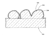
図9を参照すると、ボトム電極300が、HSG層304上に拡がる超薄型で適合した誘電体層302とともに示される。DRAMキャパシタの要求に従って、誘電体層が電流漏れ及びその結果としてのデータエラーの過大なリスクを回避するのに必要な最小の厚さで形成される。特に、ボトム電極300をコートする誘電体層302は、使用される材料に依存して、好ましくは約10Åから200Å、より好ましくは約25Åから100Åの厚みを有する。、
同時に、本明細書に開示の方法によって提供される高いステップカバレージは、上端、側壁、凹部及びネック領域表面を含むHSG層の全表面上に所望の厚さの均一な形成を可能にする。従って、HSGシリコン層304上の誘電体層302は、構造の任意の点及びプロセスの間の任意の点においてその最大厚さの好ましくは約95%以下、より好ましくは約98%以下の最小厚さを有する。
【0128】
全ての利用可能な部位の占有を抑制する化学吸着した複合体の物理的な大きさが原因で、とりわけ吸着した複合体が有機リガンドを含有する場合に、好ましい条件下で、単層のフラクションに十分な材料がサイクル毎に堆積する。表IVの例において、ZrO2は約0.75Å/サイクルで成長し、演算の電流漏れ及びデータエラーを回避するのに適切な厚さの誘電体層を製造するために、好ましくは約30から80サイクル、より好ましくは30から50サイクルが行われる。
【0129】
示していないが、次に上部電極層が誘電体層302上に形成され、加工が完成することは、当業者が容易に認識するところであろう。
【0130】
図10では、同じ参照数字は同じ部品に対して使用されており、同様なボトム電極300が、HSGシリコン層304上の同様な適合した(conformal)誘電体層302とともに示される。加えて、バリアー層306が、誘電体302とHSGシリコン表面304との間に形成される。例えば、上記表II及びIIIの例に従って、熱的に成長したシリコン窒化物層が、酸化タンタル誘電体302の下でバリアー層306として役目を果たす。このように、容易に酸化されるHSGシリコン304は酸化から幾分保護される。シリコン窒化物は、有効にキャパシタ誘電体の一部になり、有効な誘電率を低下させるが、下部電極300を酸化から一層よく保護する。
【0131】
図11では、ボトム電極300は、HSGシリコン層304上に適合的に拡がる進行中のナノラミネート誘電体302を概略的に示す。部分的に加工された誘電体スタック302は、好ましくは、約3Åから10Åの第一誘電体下部層(first dielectric sublayer)302a(例えば、5Å TiO2);約3Åから10Åの第二誘電体下部層(例えば、5Å Ta2O5);約3Åから10Åの第三誘電体下部層(例えば、5Å TiO2);などを含む。同様な又は異なる構造のいくつか付加的な層を、漏れのないメモリーセルキャパシタを完成するために加えうることは、理解されるであろう。
【0132】
図12では、HSGシリコン304を含むキャパシタボトム電極300は、図9に関する記載のように、その上に適合する超薄型の高k誘電体302を有する。加えて、図12は、高k誘電体302上に形成された上部電極を示す。上部電極は、有利には、高k誘電体上にALDによって直接的に形成された初期導電薄膜308を含む。導電薄膜308は表VII及び/又は表VIIIに記載のALDプロセスによって堆積するので、導電層308はキャパシタ誘電体を適合的にコートし、このようにして高表面キャパシタの十分な上部電極カバレージを保証する。同時に、上部電極の残部310は、CVD又はPVDのような従来の方法によって、静電容量を損失することなく形成されうる。
【0133】
一例において、キャパシタ誘電体はTa2O5のような揮発性物質を含み、初期導電薄膜308は薄い(例えば、約10nmから30nm)バリアー層を含み、表VIIのプロセスによって形成されるTiNにより例示される。本ケースにおいて、上部電極の残部310は、好ましくは、バリアー機能に有効な厚さを残すためにさらに約100nmの金属窒化物を含む。上部電極の残部310は、好ましくは、その上に堆積した、例えば元素金属のようなより導電性の材料を含む
別の例において、初期導電薄膜308は、表VIIIのプロセスによって形成されたWによって例示される薄い(例えば、約10nmから30nm)元素金属層を含む。本ケースにおいて、上部電極の残部310は、好適には、上部電極に有用な厚みを残すために、さらに約100-500nmの導電性材料及び好ましくは元素金属を含む。
【0134】
前述の発明はある好ましい具体例として記載されたものであるが、他の具体例は当業者にとって明白であろう。例えば、プロセスが特定の誘電体材料に対して特別に供給される一方で、当業者はALD法が他の材料でキャパシタを形成することに適用されうることを容易に理解するであろう。さらに、メモリーセルキャパシタの特定のプロセスフロー及び構造に関して示されたにもかかわらず、当業者は、本明細書に開示された方法が有用であるであろうスキームの変更を理解するであろう。加えて、本明細書の開示を考慮して、他の組み合わせ、省略、置換及び改良は、当業者にとって理解されるであろう。従って、本発明は、好ましい例の詳述によって制限されることを意図しないし、そのかわりに添付の請求項の参照によって定義される。
【図面の簡単な説明】
【図1】図1は、半球状粒子(HSG)シリコンを組込む、集積されたスタック型(スタッド)キャパシタメモリーセルの概略断面図である。
【図2】図2は、HSGシリコンを組込む、他の集積されたスタック型(円筒型)キャパシタメモリーセルの概略断面図である。
【図3】図3は、HSGシリコンを組込む、集積されたトレンチキャパシタメモリーセルの概略断面図である。
【図4】図4は、HSGに慣用されている化学気相成長(CVD)で形成された誘電体を組込んだキャパシタの一部の拡大図である。
【図5】図5は、HSGシリコン上にコンフォーマルな誘電体層とともにメモリーセルを形成する方法を一般に例示するフローチャートである。
【図6】図6は、HSGシリコン上にコンフォーマルな三元誘電体材料とともにメモリーセルを形成する方法をより詳しく例示するフローチャートである。
【図7】図7は、本発明の好ましい実施態様に従い、二元誘電体層を堆積するための、例示的ガスフローダイヤグラムである。
【図8】図8は、好ましい実施態様に従い、三元誘電体層を堆積するための、例示的ガスフローダイヤグラムである。
【図9】図9は、HSGシリコン上にコンフォーマルな超薄型の誘電体を含む、メモリーセルキャパシタの部分的な概略断面図である。
【図10】図10は、バリアー層およびHSGシリコン上にコンフォーマルな超薄型の誘電体を含む、一部加工されたメモリーセルキャパシタの部分的な概略断面図である。
【図11】図11は、HSGシリコン上にナノラミネート誘電体を含む、一部加工されたメモリーセルキャパシタの部分的な概略断面図である。
【図12】図12は、コンフォーマルな超薄型の誘電体およびコンフォーマルなバリアー層の両方をその上に含む、HSGシリコンボトム電極を有するメモリーセルキャパシタの部分的な概略断面図である。
【符号の説明】
10:メモリー用セル
11:キャパシタ
12:基板
14:ゲートスタック
16:ドープされた活性な領域
18:コンタクト(contact)
20:絶縁層
22:ボトム電極
24:キャパシタ誘電体層
26:上部電極
28:HSGシリコンマイクロ構造
10a:メモリー用セル
11a:キャパシタ
12:基板
22a:ボトム電極
24a:キャパシタ誘電体層
26a:上部電極
28a:HSGシリコンマイクロ構造
30:メモリー用セル
31:トレンチキャパシタ
32:基板
34:ゲートスタック
36:ドープされた活性な領域
42:ボトム電極
44:キャパシタ誘電体層
46:上部電極
48:HSGシリコン層
50:HSGシリコン層
52:半球状粒子
54:基板
56:誘電体層
60:ネック領域
61:粒子のトップ表面
62:凹角の側面
64:空洞(void)
300:ボトム電極
302:誘電体層
304:HSG層
306:絶縁層
302a:第1誘電体部分層
302b:第2誘電体部分層
302c:第3誘電体部分層
308:初期誘電薄膜
310:上部電極の残部[0001]
BACKGROUND OF THE INVENTION
The present invention generally forms a thin film on a textured bottom electrode and, more particularly, a memory cell comprising hemispherical grain (HSG) silicon in a high dielectric constant dielectric and top electrode material. It relates to providing almost perfect conformality on the bottom electrode.
[0002]
[Prior art and problems]
When processing an integrated circuit, layers of insulating material, conductive material and semiconductor material are deposited and patterned layer by layer to create the desired circuit. Many types of circuits incorporate capacitors, each of which includes a dielectric layer sandwiched between two plates or electrodes. Memory chips such as dynamic random access memory (DRAM) specifically use capacitors to store charge in memory cells. Each memory cell can represent one bit of data, where the capacitor is charged and discharged to represent a logical state.
[0003]
In accordance with general trends in the semiconductor industry, integrated circuits are shrinking in pursuit of faster processing speeds and lower power consumption. As the packing density of memory chips continues to increase, each capacitor in a denser memory cell has a certain minimum charge storage to ensure reliable operation of the memory cell without excessive refresh cycling. Still have to maintain. With the progressive generation of circuit designs, capacitor designs are thus important to achieve even higher stored charges for the shrinking area of the chip (or footprint) assigned to each cell. is there. Techniques have therefore been developed to increase the total charge capacity of cell capacitors for a given footprint allocation.
[0004]
The amount of charge stored on the capacitor is the capacitance, C = kk0A / d, where k is the dielectric constant of the capacitor dielectric between the two electrodes;0Is the vacuum dielectric constant; A is the electrode surface area; and d is the spacing between the electrodes, and also represents the thickness of the interelectrode dielectric. Early technology focused on increasing the effective surface area of the electrodes by creating a folded structure for stacked or trench capacitors. A trench capacitor is formed in a semiconductor substrate in which a transistor is generally formed, while a stacked capacitor is formed on the transistor. Such a structure makes better use of the available chip area by creating a three-dimensional shape that the conductive electrode and capacitor dielectric match.
[0005]
FIG. 1 illustrates a
[0006]
FIG. 2 illustrates, for example, a
[0007]
FIG. 3 illustrates a
[0008]
However, relying solely on such a structure to increase the capacitance of the memory cell becomes impractical due to the progressive generation of memory chip integrated designs. The surface area of the stud capacitor can theoretically be increased indefinitely simply by increasing the height of the bottom electrode. Similarly, the depth of a trench capacitor can be increased to approximately the thickness of the substrate in which it is formed. Unfortunately, there are limitations on the height or depth of shapes in integrated circuits. As is known in the art, it can be difficult to coat shapes, wrinkle or smear to fit in an advanced step using conventional deposition techniques. Furthermore, the increased topography on the chip can adversely affect the resolution of subsequent photolithography processes.
[0009]
Therefore, rather than relying solely on the height or depth of the cell capacitor, to further increase the surface area of the capacitor electrode by providing a textured or rough surface for the macrostructure fold of the bottom electrode In addition, a microstructure can be added. For example, as disclosed in U.S. Patent No. 3,405,801 issued to Han et al., A polycrystalline conductive material can be roughened, for example, preferably by etching along grain boundaries. Alternatively, U.S. Patent No. 5,372,962 issued to Hirota et al. Describes various selective etch processes for drilling holes in polysilicon layers.
[0010]
Another type of electrode texturing technique relates to the formation of hemispherical particle (HSG) silicon. Deposited polysilicon selectively grows directly on the nucleation site and redistribution annealing of amorphous silicon where thermal energy moves silicon atoms around the surface and aggregates in a nodule per nucleation site Several methods are known for forming HSG silicon, including: FIGS. 1 and 2 show a bottom electrode 22, 22a that includes
[0011]
In order to fully realize the benefits of the increased surface area of the textured bottom electrode, the capacitor dielectric layer should closely fit the surface of the bottom electrode. The dielectric thickness (capacitance type “d” above) should be minimized to maximize capacitance, while too thin capacitor dielectric is There is a risk of leakage current. Leakage currents can occur as a result of pinholes in the dielectric and the quantum tunneling effect, both of which are more likely to occur with thinner dielectrics. The thin capacitor dielectric layer is thus characterized by a low breakdown voltage, limiting the charge that can be stored on the bottom electrode before breakdown leakage occurs. Thus, the capacitor dielectric layer can be characterized by the minimum thickness required to avoid breakdown, depending on the dielectric material selected.
[0012]
With reference to FIG. 4, an enlarged view of the
[0013]
As shown, the
[0014]
Independent of variations across the workpiece, non-uniformity also results in micro-levels on the bumpy surface. In particular, at the
[0015]
If the dielectric 56 is deposited to a minimum thickness in the
[0016]
In part, due to such limitations in capacitance increased by increasing electrode surface area, more recent attention has instead focused on ways to increase the dielectric constant (k) of the capacitor dielectric. . Much effort is directed to incorporating new dielectric materials with higher k values. High-k material is aluminum oxide (Al2OThree), Tantalum oxide (Ta2OFive), Barium strontium titanate (BST), strontium titanate (ST), barium titanate (BT), lead zirconium titanate (PZT), and strontium bismastantalate (SBT). These materials are characterized by an effective dielectric constant that is significantly higher than conventional dielectrics (eg, oxide and silicon nitride). While k for silicon dioxide is 3.9, the dielectric constants of these new materials can range from approximately 10 (aluminum oxide) to 300 (BST), some higher (600-800). By using such materials, the cell capacitance / footprint can be greatly increased.
[0017]
Furthermore, dramatically increasing the k value of the capacitor dielectric can use smaller and simpler capacitor designs for a given stored charge requirement. The need to reduce the surface area of a cell capacitor can simplify the integration process and allow greater packing density for future circuit designs.
[0018]
However, incorporating high-k materials into conventional process flows has proven difficult. Ta2OFiveSome materials, such as BST and other “odd” materials, tend to be very oxidative, related to high temperature deposition and post deposition annealing conditions, oxidation of traditional electrode materials, and more Even diffusion of oxygen to the lower circuit elements occurs. ZrO2And TiO2Other materials such as have very inconsistent properties that depend on a variety of process conditions.
[0019]
Thus, there is a need for a more effective method for increasing the storage capacitance of embedded memory cells.
[0020]
[Means for Solving the Problems]
Summary of invention
To meet this need, a method is provided herein for depositing dielectric and top electrode materials on a textured bottom electrode surface. Advantageously, the method requires that high conformality be achieved, so that the minimum required thickness required for the lining layer is formed on the entire surface. The method allows the deposition of high dielectric constant (high k) material on hemispherical particle (HSG) silicon under conditions favorable to maintain the silicon electrode.
[0021]
In general, the method includes cycles of alternating reactant phases, where each phase has a self-limiting effect. Metal oxides and ternary materials having a dielectric constant greater than about 10 can be formed by alternately adsorbing self-terminated metal or silicon composite monolayers by a ligand exchange reaction. The ligand present on the adsorbed metal or silicon complex is subsequently removed by the presence of oxygen-containing species, leaving OH groups and oxygen bridges in place of the halide or organic monolayer. Herein, examples are provided for nanolaminates comprising alternating simple binary metal oxides, ternary materials such as metal silicates, and alternating ultrathin dielectric layers of different compositions.
[0022]
Advantageously, the method allows a uniformly thick dielectric layer on HSG silicon to be formed as thin as possible, preferably without inducing leakage current due to the capacitor dielectric so formed. . Furthermore, the method facilitates the combination of high-k materials and high surface area textured electrodes. Thus, the capacitance is maximized, facilitating further scaling of the critical dimension without loss of cell reliability.
[0023]
Similar alternating components are preferably used to form the top electrode material on the conformal dielectric layer. Illustrated herein are examples of metal nitride barriers as well as elemental metal layers. Following the formation of a thin conformal conductive layer by a preferred method, conventional deposition with reduced conformality can complete the desired thickness of the top electrode without sacrificing capacitance. . The conformal capacitor dielectric and top electrode formed by the preferred method thus fully exploits the benefits of increased surface area caused by the textured bottom electrode.
[0024]
DETAILED DESCRIPTION OF THE INVENTION
Although described in connection with certain preferred materials, it is understood that the methods and structures described in light of the disclosure herein apply to a variety of other materials suitable for capacitor dielectrics on uneven surfaces. Is done. Further, while exemplifying with respect to memory cell storage capacitors, those skilled in the art will describe to other rough surface electrodes, such as the floating gate electrode of electrically erasable programmable read only memory (EEPROM) devices. The application of the proposed method is easily recognized.
[0025]
As discussed in the prior art section above, conventional chemical vapor deposition (CVD) capacitor electrodes, and specifically electrode structure coatings with hemispherical particle (HSG) silicon, are fully Conformity that is less than Although many studies have generally contributed to obtaining more conformal step coverage of semiconductor step features, it is very difficult to deliver the same concentration of deposited species to the entire surface of such structures. It is difficult to. In particular, it is difficult to supply the same concentration of deposited species on the top surface of the HSG particles, as is supplied to the neck region between the particles. This problem is particularly exacerbated when the textured electrode is compatible with three-dimensional folded structures such as the stacked and trenched designs of FIGS. 1-3, and is further enhanced with structures having an internal volume such as that of FIG. Getting worse. Therefore, the full advantage of the increased surface area of HSG silicon is not realized.
[0026]
By providing almost complete step coverage, the preferred embodiment advantageously obtains the minimum required thickness for the desired capacitor dielectric layer over the entire surface of the HSG particles. Desirably, the method of the preferred embodiment is less dependent on the relative concentration of reactant species on the particles as compared to the restricted particle intersection.
[0027]
Furthermore, the preferred embodiment provides a high-k material deposition method to allow high surface area textured surfaces and silicon electrode integration, which results in microstructural rough surfaces such as HSG morphology. Most often used. Rather than presenting a choice between a high surface area texture on a three-dimensional folded structure and a high-k dielectric, the preferred embodiment is a very high capacitance / foot in a repeatable, high-value manner. Enable both techniques to achieve printing.
[0028]
Preferred embodiments are formed by Al2O3 (k-10), ZrO2 (k-12-20), TiO2 (k-20-50), mixed zirconium silicon oxide (k-8-13), and combinations of the above An exemplary method for depositing a nanolaminate dielectric is provided. Similarly, a method is provided for depositing electrode materials on dielectric and HSG silicon. These materials are all formed by a method that is compatible with HSG silicon, resulting in almost perfect conformality. Thus, the preferred embodiment allows for increased capacitance not only with high-k dielectric materials, but also by full utilization of the increased surface area caused by HSG silicon. Such conformality is obtained even on high aspect ratio structures, such as stacked and trench capacitor designs.
[0029]
Further advantages of the preferred method will become apparent from the discussion below.
[0030]
Method for forming conformal capacitor dielectric
FIG. 5 generally illustrates a method of forming a capacitor dielectric layer with high step coverage. A preferred method is in the form of atomic layer deposition (ALD) whereby the reactants are fed to the workpiece in a pulse exchange during the cycle. Preferably, each cycle forms no more than about 1 monolayer of material by adsorption, more preferably by chemisorption. The substrate temperature is maintained within a window that promotes chemisorption. In particular, the substrate temperature is maintained at a sufficiently low temperature to maintain an intact bond between the adsorption complex and its underlying surface and to prevent precursor degradation. On the other hand, the substrate temperature is maintained at a sufficiently high level to avoid condensation of the reactants and to provide activation energy for the desired surface reaction during each phase. Of course, the preferred temperature window for any given ALD reaction will depend on the surface ends involved and the reactant species.
[0031]
Each pulse or phase of each cycle is preferably self-limiting in effect. In the example below, each of the phases is self-terminated (i.e., an adsorbed and preferably chemisorbed monolayer is left with a surface that is non-reactive with the components of that phase. ). Excess reactant precursor is fed in each phase to saturate the structural surface. Surface saturation ensures that the reactants occupy all available reactive sites (subject to physical size limitations, as discussed in more detail below), while self-termination is more In locations subjected to long exposure, excessive film growth is impeded. The overall utilization of saturation by chemisorption, i.e. self-terminating components, ensures excellent step coverage.
[0032]
Prior to forming the dielectric layer, the integrated circuit is first partially processed in that the capacitor is built on the bottom or bottom electrode. Typically, the bottom electrode functions as a storage electrode in the memory cell. However, for the purposes of this description, the bottom electrode is the capacitor electrode or plate that was originally formed, regardless of whether it functions as a storage or reference plate in a complete integrated circuit. Indicates.
[0033]
As shown in FIG. 5, the method according to the preferred binary material embodiment begins with the
[0034]
After formation of the bottom electrode macrostructure, in either a stack or trench arrangement, the bottom electrode is subsequently provided with a textured or rough microstructure overlaid on a three-dimensional folded
[0035]
ASM, International, Inc. trade name A600 UHVTMIn an exemplary process performed in a batch system sold at, HSG silicon is formed by amorphous silicon deposition, seeding and redistribution annealing. A three-dimensional folded structure is formed or coated with amorphous silicon. In some methods, the folded amorphous silicon structure is A600 UHV, although amorphous silicon deposition can be performed in situ in the illustrated embodiment in the same reaction chamber as subsequent steps.TMFormed before transferring the wafer to the system.
[0036]
In a preferred reactor, the amorphous silicon surface is seeded. In the illustrated embodiment, the temperature is increased to a level in the range of about 550 ° C to 575 ° C (eg, about 560 ° C), but the reactor pressure is preferably reduced to the order of about 10-5 Torr. The seeding gas in the preferred embodiment is monosilane, supplied at a silane partial pressure of about 4 × 10 −6 Torr. After seeding, its density can change by design, and sustained heat treatment at the desired temperature results in redistribution of mobile amorphous silicon. Silicon atoms tend to aggregate around the seed or nucleation site formed by the silane. The entire method occurs on the order of about 10 and 120 minutes for batch systems including temperature ramps, seeding and annealing. Those skilled in the art will readily recognize many other techniques for forming HSG silicon.
[0037]
HSG particles made by a preferred method can range in size from about 50 to 750 cm, more typically from about 300 to 500 cm. Process conditions that affect nucleation density and HSG silicon particle size are typically selected to leave particles that are significantly separated from one another. Such an arrangement maximizes the electrode surface area within the limits of fitting most of the subsequent dielectric and top electrode layers between the particles. However, as will be appreciated from the enlarged views of FIGS. 9-12, the particles are randomly concentrated at several locations due to the inherent random seeding process. Furthermore, the preferred dielectric and top electrode layers allow the use of denser and less distant particles, thus increasing the usable surface area.
[0038]
As will be appreciated by those skilled in the art, the bottom electrode preferably functions as a storage node for memory cells in a dynamic random access memory (DRAM) array. After processing, the bottom electrode is typically isolated from the bottom electrodes of other cells across the array, as shown in FIGS. 1A, 1B and 2.
[0039]
The so-formed bottom electrode structure is then coated with high step coverage. According to a preferred embodiment, the dielectric layer is formed in a periodic manner, where each cycle forms about 1 or less monolayer dielectric material on the workpiece in a self-limiting manner. Preferably, each cycle includes at least two different phases, where each phase leaves a saturation reaction, ie, about 1 or less atomic monolayer of the desired dielectric material in a self-limiting manner.
[0040]
If necessary, the exposed surface of the bottom electrode (eg, HSG silicon of the preferred embodiment) is terminated 102 and reacted with the first phase of the ALD method. The first phase of preferred metal oxide embodiments (see Tables I-V) is reactive with, for example, hydroxyl (OH) or ammonia (NH3) termination. In the examples below, the silicon surface of HSG silicon generally does not require a separate termination. Exposure to a clean indoor environment results in natural oxide formation that naturally provides an
[0041]
After the
[0042]
The metal-containing reactive species is preferably supplied in gaseous form and is therefore referred to below as the metal source gas. The first component is subsequently removed 106 from the reaction chamber. In the illustrated embodiment, step 106 simply requires stopping the flow of the first component while continuing to flow the carrier gas for a sufficient amount of time, preferably about twice or more the reaction chamber volume, more preferably Excess reactants and reactant by-products are diffused or purged from the reaction chamber using a purge gas that is at least about three times the chamber volume. In the illustrated embodiment,
[0043]
When the unreacted (or excess) reactant of the first component is removed 106 from the chamber, the second component is fed 108 to the workpiece. The second component desirably reacts with the self-terminated monolayer formed in
[0044]
In other arrangements, the second component simply removes the ligand termination of the adsorbed metal complex monolayer formed in step 104 (eg, by sublimation or reduction), or the oxidation or further component oxidation or Monolayers for chemisorption can be prepared.
[0045]
Desirably,
[0046]
After sufficient time to fully saturate the surface of the metal composite monolayer by chemisorption (or self-limiting reaction) of the second component, the excess second component is removed 110 from the workpiece. As with the
[0047]
In the illustrated embodiment, once the excess reactants and by-products of the second component have been purged from the reaction chamber, the two phases alternate so that the first phase of the ALD process is repeated. Thus, the
[0048]
The two
[0049]
With reference to FIG. 6, additional components may also be included in each cycle. In FIG. 6, the steps corresponding to those of FIG. 5 are referred to by numbers having the same last two digits in the 200 series rather than the 100 series of FIG. Thus, steps 200-210 are similar to the corresponding steps 100-110 of FIG.
[0050]
However, the illustrated
[0051]
In particular, after the first metal /
[0052]
Although the illustrated method includes four phases in each
[0053]
The second metal / silicon source gas in the
[0054]
The oxygen source gas in the
[0055]
[0056]
Both the binary and ternary methods are illustrated in FIGS. 5 and 6 by the initial metal / silicon phase and the subsequent oxygen phase in the examples below, but the cycle depends on lower surface and phase components. Thus, it is understood that it can begin in the oxygen phase.
[0057]
【Example】
Method for forming a metal oxide dielectric
FIG. 7 and Tables I-V below illustrate an exemplary process for forming a metal oxide dielectric on bottom electrode HSG silicon. Table I illustrates the formation of oxides of non-transition metals (eg, aluminum); Tables II and III illustrate the formation of oxides of Group V transition metals (eg, vanadium, niobium, tantalum); Tables IV and V illustrate oxide formation of group IV transition metals (eg, titanium, zirconium, hafnium). For simplicity, similar reference numerals are used to refer to the phases and steps of the example metal oxide (FIG. 7), corresponding to the general description of FIG.
[0058]
Referring to FIG. 7, the gas flow procedure is represented consistent with a special embodiment. In the described embodiment, a high-k dielectric, and more particularly a high-k metal oxide, is formed by alternately supplying a metal source gas and an oxygen source gas to a work piece in the manufacturing process. The The first or
[0059]
The surface on which the dielectric material is formed is first terminated to provide a surface that reacts with the metal source gas. In a preferred embodiment, the exposed surface on which deposition is desired comprises HSG silicon with OH termination (see FIG. 9) and silicon nitride (see FIG. 10).
[0060]
Most preferably, the
[0061]
Stopping the flow of the metal source gas stops the
[0062]
During the
[0063]
In particular, the metal-containing species provided to the product in the manufacturing process is self-terminating so that the adsorbed composite surface will not react further with the metal source gas. In the examples described below, TMA (Table I) represents a single layer of methyl-terminated aluminum. Tantalum ethoxide (Table II) leaves a single layer of ethoxide tantalum. Similarly, other volatile metal halides will leave a halide-terminated surface and organometallic precursors will leave a surface terminated with an organic ligand. Such a surface does not react further with the metal source or other reactant flow components during the metal
[0064]
In the
[0065]
During the
[0066]
In particular, the oxygen source gas reacts with the ligand of the metal complex chemisorbed on the surface of the product in the manufacturing process during the previous pulse of the metal source gas. The reaction is also surface limited or terminated. This is because the oxidant during
[0067]
The metal phase 107 (including the
[0068]
[0069]
The table below provides an exemplary process approach for forming metal oxide and ternary dielectric layers suitable for capacitor dielectric applications in DRAM memory cells for very large scale integrated processing. The dielectric is particularly suitable for deposition on HSG silicon. Each process approach represents one cycle in a single wafer process module. In particular, the parameters described are trade names Pulsar 2000 which are commercially available from ASM Microchemistry Ltd., Finland.TMDeveloped for use in single wafer ALD modules, which are commercially available.
[0070]
Note that the parameters in the table below are exemplary only. Each process phase is preferably arranged to saturate the bottom electrode surface. The purge step is arranged to remove reactants during the reactive phase from the reaction chamber. The illustrative ALD process achieves a thickness uniformity of about 95% or more, and more preferably about 98% or more, on HSG particles having an average particle size of about 400 mm. Thickness uniformity is defined as the percentage of the minimum thickness as a percentage of the maximum thickness as used herein. In view of the disclosure herein, to achieve a self-terminating phase saturated with an acceptable deposition rate, one of ordinary skill in the art would immediately move the deposition conditions to different reaction chambers and different selected conditions. It can be modified, substituted or otherwise altered.
[0071]
Advantageously, the ALD process described herein is relatively insensitive to pressure and reactant concentration so long as the reactant feed is sufficient to saturate the textured surface. Furthermore, the process can be performed at low temperatures. The temperature of the product in the manufacturing process is preferably maintained between about 150 ° C. and 350 ° C. during the process to achieve a relatively fast deposition rate while maintaining a thermal budget. More preferably, the temperature is maintained between about 220 ° C. and 300 ° C. depending on the reactants. The pressure in the chamber can range from the milliTorr range to the super-atmospheric range, but is preferably maintained at about 1 Torr to 500 Torr, more preferably about 1 Torr to 10 Torr. The
[0072]
[Table 1]
[0073]
In the first phase of the first cycle, TMA chemisorbs onto the bottom electrode HSG silicon surface. The metal source gas preferably includes a sufficient carrier flow rate given other process parameters to saturate the bottom electrode surface. A monolayer of aluminum composite is left on the HSG silicon surface, which monolayer is self-terminating at the methyl end.
[0074]
After the TMA flow is stopped and purged by the continued carrier gas flow, H2A pulse of O is supplied to the product in the manufacturing process. The water reacts immediately with the methyl end surface of the metal monolayer in a ligand exchange reaction to produce aluminum oxide (Al2OThree). The reaction is limited by the number of available metal complexes that have been chemisorbed beforehand. Furthermore, the reaction is self-limiting in that neither water nor carrier gas reacts further with the hydroxyl and oxygen bridge ends of the resulting aluminum oxide monolayer. Furthermore, suitable temperature and pressure parameters suppress the diffusion of water or reaction byproducts across the metal monolayer.
[0075]
In the next cycle, the first phase introduces TMA, which immediately reacts with the surface of the aluminum oxide monolayer, and again over the first metal oxide layer, methyl-terminated aluminum. Leave a layer. Next, the second phase of the second cycle is as described for the first cycle. These cycles are repeated until the desired thickness of aluminum oxide is formed.
[0076]
In the illustrated embodiment, the carrier gas continues to flow at a constant rate during both phases of each cycle. However, it will be appreciated that the reactants can be removed by evacuating the chamber between alternating gas pulses. In one arrangement, the preferred reactor incorporates hardware and software to maintain a constant pressure during pulse deposition. The publications of U.S. Patent No. 4,747,367 issued May 31, 1988 to Posa and U.S. Patent No. 4,761,269 issued August 2, 1988 to Conger et al. Are hereby incorporated by reference.
[0077]
The radicals provided by the plasma generator can facilitate the deposition of the metal-containing layer at the low temperature of the ALD process. The structure and method of layer deposition with radical enhancement is the title of the invention filed on September 8, 1999, called IMPROVED APPARATUS AND METHOD FOR GROWTH OF A THIN FILM, Provided in a patent application having Serial No. 09 / 392,371, the disclosure of which is incorporated by reference above. Another exemplary ALD process flow is provided in US Patent No. 5,916,365 to Sherman, issued June 29, 1999, the disclosure of which is hereby incorporated by reference.
[0078]
[Table 2]
[0079]
After barrier layer formation, Ta2OFiveIs formed by ALD process. As shown in Table II, the described metal source gas is tantalum ethoxide (Ta (OCH2CHThree)FiveCarrier gas is nitrogen (N2And the oxygen source gas is preferably ozone (OThree)including. The temperature during the process is preferably maintained at about 150 ° C to 300 ° C, more preferably about 220 ° C.
[0080]
In the first phase of the first cycle, tantalum ethoxide chemisorbs onto the nitrided surface of HSG silicon. The metal source gas preferably comprises a sufficient percentage of the carrier flow given other process parameters to saturate the nitride coated HSG silicon surface. A monolayer of tantalum composite is left on the textured surface, which monolayer is self-terminated with ethoxide termination.
[0081]
After the metal source gas flow is stopped and removed by a continuous flow of carrier gas, a pulse of ozone is supplied to the product in the manufacturing process. Ozone preferably contains a sufficient percentage of the carrier flow given other process parameters to saturate the metal-containing monolayer surface. Ozone reacts immediately with the ethoxide-terminated surface of the metal-containing monolayer in a ligand exchange reaction to produce tantalum oxide (Ta2OFive). The reaction is limited by the number of available metal complexes that have been chemisorbed beforehand. Neither ozone nor carrier gas reacts any further with the resulting tantalum oxide monolayer. Ozone burns organic ligands and CO2And H2O is released and the monolayer leaves behind hydroxyl and oxygen bridge ends. Furthermore, suitable temperature and pressure parameters suppress the diffusion of ozone and reaction byproducts through the metal monolayer.
[0082]
In the next cycle, the first phase introduces tantalum ethoxide, which immediately reacts with the surface of the tantalum oxide monolayer, leaving an ethoxide terminated tantalum layer again. The second phase of the second cycle is then as described for the first cycle. These cycles are repeated until the desired tantalum oxide thickness is formed. Preferably, about 40-100 to Ta2OFiveAbout 80 to 200 cycles are performed to form More preferably, about 80-100 cycles are performed to form about 40-50 cm.
[0083]
In the described embodiment, the carrier gas continues to flow at a constant rate during both phases of each cycle. However, it will be appreciated that the reactants can be removed by evacuating the chamber between alternating gas pulses. In one arrangement, the preferred reactor incorporates hardware and software to maintain a constant pressure during pulse deposition. The disclosures of U.S. Patent No. 4,747,367 issued May 31, 1988 to Posa and U.S. Patent No. 4,761,269 issued August 2, 1988 to Conger et al. Are incorporated herein by reference.
[0084]
Amorphous Ta2OFiveThe dielectric layer is left with only a trace amount of carbon. This layer can be annealed to the crystallized dielectric, if desired. The dielectric constant of the layer is about 20-25.
[0085]
[Table 3]
[0086]
In the first phase of the first cycle, tantalum chloride chemisorbs on the silicon nitride surface of HSG. The metal source gas preferably includes a sufficient percentage of the carrier flow given other process parameters to saturate the nitride coated HSG silicon surface. A monolayer of tantalum composite is left on the textured surface, which monolayer is self-terminating at the chloride end.
[0087]
TaClFiveAfter the flow is stopped and removed by a continuous flow of carrier gas, a pulse of water vapor is delivered to the work piece in the manufacturing process. The water vapor preferably includes a sufficient percentage of the carrier flow given to other process parameters to saturate the metal-containing monolayer surface. Water reacts immediately with the chloride-terminated surface of the metal-containing monolayer in a ligand exchange reaction to produce tantalum oxide (Ta2OFive). The reaction is limited by the number of available metal chloride complexes that have been previously chemisorbed. Neither water nor carrier gas reacts any further with the hydroxyl and oxygen bridge ends of the resulting tantalum oxide monolayer. Furthermore, suitable temperature and pressure parameters suppress the diffusion of water and reaction byproducts through the metal monolayer.
[0088]
In the next cycle, the first phase introduces tantalum chloride, which immediately reacts with the surface of the tantalum oxide monolayer leaving a chloride-terminated tantalum layer again. Then the second phase of the second cycle is as described for the first cycle. These cycles are repeated until the desired thickness of tantalum oxide is formed, as described for the previous examples.
[0089]
As mentioned above, it is preferred to purge between pulses, but rather than be removed by a stable carrier gas flow as shown, the chamber can be evacuated to remove reactants between pulses.
[0090]
Amorphous Ta2OFiveThe dielectric layer is left with only a trace amount of chlorine. This layer can be annealed to the crystallized dielectric, if desired. The dielectric constant of the layer is about 20-25.
[0091]
[Table 4]
[0092]
The temperature during the process preferably falls between about 200 ° C and 500 ° C. Amorphous ZrO2For the layer, the temperature is more preferably below this range, about 200 ° C. to 250 ° C., most preferably about 225 ° C. For crystalline films, the temperature is more preferably above this range, between about 250 ° C. and 500 ° C., most preferably about 300 ° C. However, as will be appreciated by those skilled in the art, a mixture of amorphous and crystalline compositions is at the boundary of these two regions. The described process is mainly crystalline ZrO2Create a film.
[0093]
In this case, the metal monolayer formed during the metal phase is self-terminating with chloride and an excess of ZrCl under favorable conditions.FourAnd does not react immediately. However, the preferred oxygen source gas reacts with or adsorbs on the chloride end surface in a ligand exchange reaction limited by the supply of pre-adsorbed zirconium chloride complex during the oxygen phase. In addition, oxidation leaves hydroxyl and oxygen bridge ends that do not react any further with excess oxidant in the saturating phase.
[0094]
Preferably, about 20-60-60 ZrO2About 30 to 80 cycles are performed to grow. More preferably, about 30-50 cycles are performed to grow about 20-40 inches. The dielectric constant of the layer is about 18-24.
[0095]
[Table 5]
[0096]
ZrO in the previous example2As described above, the temperature is preferably maintained at a level of about 200 ° C to 500 ° C. However, in the described embodiment, the described embodiment takes a temperature between about 250 ° C. and 500 ° C., and most preferably about 300 ° C.
[0097]
In this case, the metal monolayer formed during the metal phase is self-terminating with chloride and under favorable conditions TiClFourAnd does not react immediately. However, the preferred oxygen source gas is a reaction limited by the supply of a pre-adsorbed titanium chloride complex that reacts with or adsorbs on the chloride terminated end surface during the oxygen phase. Furthermore, the oxidation leaves hydroxyl and oxygen bridges and termini that do not react any further with excess oxidant in the saturating phase.
[0098]
Preferably, about 20-60-60 TiO2About 30 to 80 cycles are performed to grow. More preferably, about 30-50 cycles are performed to grow about 20-40 inches. The dielectric constant of the layer is 15-25.
Method for forming a ternary dielectric layer
As discussed with respect to FIG. 6, the above ALD principles for metal oxide capacitor dielectrics can be extended to the deposition of ternary and more complex materials.
[0099]
With reference to FIG. 8, the gas flow block diagram illustrates the general process of forming a ternary structure, particularly the formation of mixed or compound metal oxides or metal silicates. The examples in Table VI below related to metal silicates are formed in the order of metal / oxygen 1 / silicon / oxygen 2 phase, but the disclosed order is applied to silicate materials (eg, silicon / oxygen / metal / oxygen). One skilled in the art will readily appreciate that it can be modified or adapted to complex metal oxides (eg, first metal / oxygen / second metal / oxygen). Further, the illustrated order can be extended to include more complex materials incorporating multiple elements. For convenience, reference numerals in FIG. 6 are used to refer to similar process steps, phases and sequences.
[0100]
As shown, the process includes four phases for each cycle, each phase including a reactant phase and a purge phase. First metal or
[0101]
In general, the process allows dielectric layers with mixed metal oxides, ternary metal oxide compounds, metal silicates or more complex dielectric materials. For example, TiO2Ta by alternative cycle2OFiveCan be mixed with. Most binary cycles can be repeated several times during the ternary cycle if only a slight doping effect is desired. However, in the example of Table VI below, a zirconium silicon oxide or “zirconium silicate” layer is shown.
[0102]
[Table 6]
[0103]
In the sequence described, the metal phase is followed by an oxygen phase, followed by a silicon phase and a second oxygen phase. The cycle is then repeated. In the described embodiment, two different oxygen source gases are used for the first and second oxygen phases (second and fourth phases) of each cycle, but instead the same oxygen source is used for both phases. Can be used.
[0104]
During the metal phase, the zirconium-containing monolayer is self-terminating at the chloride end. The end of this monolayer is ZrCl under the desired conditions.FourDoes not react easily. In the next phase, water vapor oxidizes the metal, including the monolayer, replacing the chloride ends with hydroxyl and oxygen bridge ends. A suitable silicon source gas is then reacted or adsorbed to the hydroxyl and oxygen bridge ends during the silicon phase in the ligand exchange reaction limited by the supply of the previously adsorbed metal oxide complex. Furthermore, suitable silicon source gases leave organic (ethoxide) or halide (chloride) ends that do not react any further with excess silicon ethoxide in the saturation phase. Finally, the silicon-containing monolayer on which ozone was previously adsorbed is oxidized, leaving a ternary oxide.
[0105]
As those skilled in the art will appreciate, the described zirconium silicate (ZrSixOyA ternary structure such as a) layer advantageously exhibits a higher dielectric constant, lower operational leakage and a more stable structure that interfaces with silicon. The Zr: Si ratio can be controlled to optimal properties depending on the relative number of four phase cycles performed compared to two phases (simple metal) in the same process. Thus, zirconium silicate is not necessarily stoichiometric.
[0106]
Preferably, about 20 to 100 cycles are about 20 to 100 ZrSixOyLead the growth. More preferably, about 20 to 40 cycles lead to growth of about 20 to 40 inches. The dielectric constant of the layer is about 10-15.
[0107]
Method for forming a dielectric stack
In contrast to the mixed or compound structure produced by the processes of FIGS. 6 and 8, the capacitor dielectric can also include a stack of different dielectric sublayers. An exemplary stack is about 5 to 40, more preferably about 10 Ta.2OFiveAnd TiO2Of alternating layers.
[0108]
Preferably, at least one of the lower layers, more preferably the entire lower layer, is formed by the same ALD as described above. FIG. 11 shows an exemplary capacitor formed by this process and discussed in more detail below.
[0109]
In the described embodiment, the above process is preferably performed for about 10 to 100 cycles to produce a high-k dielectric layer having a thickness of about 5 to 50 cm (assuming about 0.5 cm / cycle) . Preferably another dielectric material is also deposited to form a thickness of about 5-50 mm. In an exemplary process flow, the process in Table II above is about 5 mm Ta.2OFiveIs then replaced with the process of Table V, which results in about 5% of TiO2And is continued until a thickness appropriate for the memory cell capacitor application is reached.
[0110]
Like the mixed or compound layers described in Table VI, the dielectric stack or “nanolaminate” so formed tends to exhibit a stable structure due to enhanced dielectric properties and contact with silicon. is there.
[0111]
Method for forming upper electrode material
After forming the dielectric layer, an upper electrode is formed on the capacitor dielectric. If the top electrode does not fully conform to the dielectric, the full benefits of the textured bottom electrode and conformal dielectric are not realized. Thus, the top electrode formed on the capacitor dielectric preferably comprises at least one conductive thin film deposited with near-perfect conformality by an ALD process.
[0112]
The top electrode is preferably relatively thick for high lateral dielectric constant across the memory array and / or for positioning the contact thereon without risk of spikes through the capacitor dielectric. Is. However, a suitable alternating deposition process may not form the full thickness of the top electrode. Rather, one or more initial thin conductive layers can be conformally formed by a suitable alternating process followed by conventional deposition for the majority of the top electrode thickness. The alternating process provides a conductive coating in continuous direct contact with the capacitor dielectric, thereby adapting to the undulation of the underlying textured bottom electrode. The remainder of the upper electrode deposited by conventional techniques may not be conformal. Furthermore, voids can be tolerated between the initial conformal film and the remainder of the top electrode thickness as long as the initial film is properly connected to the integrated circuit circuitry.
[0113]
The initial conductive thin film may contain any suitable conductive material including silicon, metal nitrides and elemental metals, composites thereof, and nanolaminates thereof. Depending on the material of the dielectric capacitor, a barrier layer may be desired on the dielectric. Especially Ta2OFiveIf used, the barrier above it prevents oxidation of the rest of the top electrode. Thereafter, the remainder of the top electrode can be completed by conventional deposition methods of conductive films such as silicon or metal.
[0114]
In the example of Table VII below, the upper electrode contains a conductive metal nitride. The metal nitride was deposited by an ALD process that conformally and continuously coats the capacitor dielectric.2OFiveCan act as a barrier layer on top. In the example of Table VIII below, the top electrode contains an elemental metal layer and can be placed on or replaced on the barrier of Table VII and is also formed by an ALD process.
[0115]
[Table 7]
[0116]
In the first phase of the first cycle, TiClFourChemisorbs on the hydroxyl and oxygen bridge ends of the deposited high-k dielectric. The metal source gas preferably comprises a sufficient percentage of the carrier flow given other process parameters to saturate the dielectric surface. A single layer of titanium composite remains on the dielectric, which is self-terminating with a halide end tail.
[0117]
Preferably, the reactor includes a catalyst that converts the metal source gas into smaller and / or more reactive species. In the described embodiment, the preferred reaction chamber is TiClFourTiClThree +Including a titanium wall that is advantageously converted to Smaller species diffuse easily into confined spaces, occupy more reactive sites per cycle, and more easily chemisorb to active sites. Thus, the catalyst allows for faster deposition rates. One skilled in the art will readily appreciate that other catalysts can be used for other components.
[0118]
TiClFourAfter stopping the flow and purging with a continuous flow of carrier gas, NHThreeAre supplied to the workpiece. Ammonia preferably contains a sufficient proportion of carrier flow given other process parameters to saturate the surface of the metal-containing monolayer. NHThreeReacts easily with the chloride-terminated surface of a metal monolayer in a ligand exchange reaction to form a titanium nitride (TiN) monolayer. The reaction is limited by the number of available metal chloride complexes previously chemisorbed. Neither ammonia nor the carrier gas reacts any further with the produced titanium nitride monolayer. Furthermore, the preferred temperature and pressure parameters suppress the diffusion of ammonia into the metal monolayer.
[0119]
In the next cycle, the first phase is TiCl, which reacts easily with the surface of the titanium nitride monolayer.FourTo leave the chloride-terminated titanium layer again. The second phase of the second cycle is then the same as described for the first cycle. These cycles are repeated until the thickness of the titanium nitride is sufficient to exert a barrier function. Preferably, a metal nitride of about 5 nm to 50 nm, more preferably about 10 nm to 30 nm is formed by this technique.
[0120]
In the illustrated embodiment, the carrier gas continuously flows at a constant rate during both phases of each cycle. However, it will be understood that the reactants may be removed by evacuating the chamber between alternating gas pulses. In one arrangement, the preferred reactor incorporates hardware and software to maintain a constant pressure during pulse deposition. The disclosures of Posa, U.S. Pat. No. 4,747,367, issued May 31, 1988, and Conger et al., U.S. Pat. No. 4,761,269, issued August 2, 1988, are references. As incorporated herein by reference.
[0121]
[Table 8]
[0122]
In the first phase of the first cycle, WF6Chemisorbs on the hydroxyl and oxygen bridge ends of the deposited high-k dielectric or on the ends of the previously formed barrier layer. The metal source gas preferably contains a sufficient percentage of carrier flow given other process parameters to saturate the dielectric surface. A single layer of tungsten composite is left on the dielectric, which is self-terminating at the remaining halide ends.
[0123]
WF6After stopping the flow and purging with a continuous flow of carrier gas, a pulse of TEB is supplied to the workpiece. The TEB preferably contains a sufficient percentage of carrier flow given other process parameters to saturate the surface of the metal-containing monolayer. TEB easily reduces the halide-terminated surface of a metal-containing monolayer, leaving a tungsten monolayer. The number of available metal halide complexes previously chemisorbed limits the reaction. Neither TEB nor the carrier gas reacts any further with the produced tungsten monolayer. Furthermore, the preferred temperature and pressure parameters inhibit TEB from diffusing into the metal monolayer.
[0124]
In the next cycle, the first phase is the WF that reacts easily with the surface of the tungsten monolayer6And a halide-terminated tungsten layer is formed again. The second phase of the second cycle is then performed as described for the first cycle. These cycles are repeated until the desired thickness of tungsten is formed. Preferably, tungsten of about 5 nm to 50 nm, more preferably about 10 nm to 30 nm provides continuous and conformal coverage to fully exploit the high surface area of the underlying bottom electrode and capacitor dielectric layer. Guarantee.
[0125]
In the described embodiment, the carrier gas continuously flows at a constant rate during both phases of each cycle. However, it will be understood that the reactants can be removed by evacuating the chamber between alternating gas pulses. As an arrangement, the preferred reactor incorporates hardware and software to maintain a constant pressure during pulse deposition. The disclosures of Posa, U.S. Pat. No. 4,747,367, issued May 31, 1988, and Conger et al., U.S. Pat. No. 4,761,269, issued August 2, 1988, are references. As incorporated herein by reference.
[0126]
After the ALD formation of the initial conductive thin film, preferably by a process similar to the process of Table VII and / or Table VIII, a conventional deposition process can form the remainder of the top electrode. Even CVD and PVD can be further used for the deposition of conductive materials from 100 nm to 500 nm. Conventional deposition methods will generally not coat the initial thin film with high step coverage, and therefore are based on a base electrode, extended by a highly conformal dielectric and initial conductive thin film provided by the bottom electrode. It will not conform exactly to the texture. However, incomplete step coverage due to bulk deposition will not result in a loss of capacitance because the initial conductive film ensures continuous and conformal coverage of the capacitor dielectric by a portion of the top electrode. .
[0127]
Structure of manufactured capacitor
Referring to FIG. 9, a
At the same time, the high step coverage provided by the method disclosed herein allows for the uniform formation of the desired thickness on the entire surface of the HSG layer including the top, sidewall, recess and neck region surfaces. Accordingly, the
[0128]
Due to the physical size of the chemisorbed complex that suppresses the occupancy of all available sites, a monolayer fraction can be obtained under favorable conditions, especially when the adsorbed complex contains an organic ligand. Sufficient material is deposited every cycle. In the example of Table IV, ZrO2Is grown at about 0.75 kg / cycle, preferably about 30 to 80 cycles, more preferably 30 to 50 cycles to produce a dielectric layer of appropriate thickness to avoid computational current leakage and data errors. A cycle is performed.
[0129]
Although not shown, those skilled in the art will readily recognize that the top electrode layer is then formed on the
[0130]
In FIG. 10, the same reference numerals are used for the same parts, and a similar
[0131]
In FIG. 11, the
[0132]
In FIG. 12, a
[0133]
In one example, the capacitor dielectric is Ta2OFiveThe initial conductive
In another example, the initial conductive
[0134]
While the foregoing invention has been described as a preferred embodiment, other embodiments will be apparent to those skilled in the art. For example, while the process is specifically tailored for a particular dielectric material, those skilled in the art will readily understand that the ALD method can be applied to form capacitors with other materials. Furthermore, despite being shown with respect to a specific process flow and structure of a memory cell capacitor, those skilled in the art will appreciate the scheme changes that would make the method disclosed herein useful. In addition, other combinations, omissions, substitutions, and improvements will be apparent to those skilled in the art in view of the disclosure herein. Accordingly, the invention is not intended to be limited by the details of the preferred examples, but instead is defined by reference to the appended claims.
[Brief description of the drawings]
FIG. 1 is a schematic cross-sectional view of an integrated stacked (stud) capacitor memory cell incorporating hemispherical particle (HSG) silicon.
FIG. 2 is a schematic cross-sectional view of another integrated stacked (cylindrical) capacitor memory cell incorporating HSG silicon.
FIG. 3 is a schematic cross-sectional view of an integrated trench capacitor memory cell incorporating HSG silicon.
FIG. 4 is an enlarged view of a portion of a capacitor incorporating a dielectric formed by chemical vapor deposition (CVD) commonly used in HSG.
FIG. 5 is a flowchart generally illustrating a method of forming a memory cell with a conformal dielectric layer on HSG silicon.
FIG. 6 is a flow chart illustrating in more detail a method of forming a memory cell with a conformal ternary dielectric material on HSG silicon.
FIG. 7 is an exemplary gas flow diagram for depositing a binary dielectric layer in accordance with a preferred embodiment of the present invention.
FIG. 8 is an exemplary gas flow diagram for depositing a ternary dielectric layer according to a preferred embodiment.
FIG. 9 is a partial schematic cross-sectional view of a memory cell capacitor including a conformal ultra-thin dielectric on HSG silicon.
FIG. 10 is a partial schematic cross-sectional view of a partially fabricated memory cell capacitor including a conformal ultra-thin dielectric on a barrier layer and HSG silicon.
FIG. 11 is a partial schematic cross-sectional view of a partially fabricated memory cell capacitor including a nanolaminate dielectric on HSG silicon.
FIG. 12 is a partial schematic cross-sectional view of a memory cell capacitor having an HSG silicon bottom electrode that includes both a conformal ultra-thin dielectric and a conformal barrier layer thereon.
[Explanation of symbols]
10: Memory cell
11: Capacitor
12: Board
14: Gate stack
16: doped active region
18: Contact
20: Insulation layer
22: Bottom electrode
24: Capacitor dielectric layer
26: Upper electrode
28: HSG silicon microstructure
10a: Memory cell
11a: Capacitor
12: Board
22a: Bottom electrode
24a: Capacitor dielectric layer
26a: Upper electrode
28a: HSG silicon microstructure
30: Memory cell
31: Trench capacitor
32: Board
34: Gate stack
36: doped active region
42: Bottom electrode
44: Capacitor dielectric layer
46: Upper electrode
48: HSG silicon layer
50: HSG silicon layer
52: hemispherical particles
54: Board
56: Dielectric layer
60: Neck area
61: Top surface of particles
62: Recessed side
64: void
300: Bottom electrode
302: Dielectric layer
304: HSG layer
306: Insulating layer
302a: first dielectric partial layer
302b: second dielectric partial layer
302c: Third dielectric partial layer
308: Initial dielectric thin film
310: The rest of the upper electrode
Claims (49)
第2材料の1以下の単層を残すために、第2反応物種を第1材料と反応させること、を包含し、ここで前記第1反応物種がハロゲン化ジルコニウムを含み、第2反応物種が酸素含有源ガス(source gas)を含む、方法。A method of forming a capacitor in an integrated circuit, comprising building a bottom electrode comprising a textured silicon layer having a hemispherical particle (HSG) morphology; and 10 directly on the textured silicon layer. Depositing a dielectric layer having a dielectric constant greater than wherein the deposition is carried out on the textured silicon layer by exposure to a first reactant species. Forming no more than one monolayer of a first material that is self-terminated by; and reacting a second reactant species with the first material to leave no more than one monolayer of the second material. Wherein the first reactant species comprises zirconium halide and the second reactant species comprises an oxygen-containing source gas.
第2材料の1以下の単層を残すために、第2反応物種を第1材料と反応させること、を包含し、ここで前記第1材料がエトキシド終結タンタルを含み、第2反応物種が酸素含有源ガスを含む、方法。A method of forming a capacitor in an integrated circuit, comprising building a bottom electrode comprising a textured silicon layer having a hemispherical particle (HSG) morphology; and 10 directly on the textured silicon layer. Depositing a dielectric layer having a dielectric constant greater than wherein the deposition is carried out on the textured silicon layer by exposure to a first reactant species. Forming no more than one monolayer of a first material that is self-terminated by; and reacting a second reactant species with the first material to leave no more than one monolayer of the second material. Wherein the first material comprises ethoxide-terminated tantalum and the second reactant species comprises an oxygen-containing source gas.
Applications Claiming Priority (2)
| Application Number | Priority Date | Filing Date | Title |
|---|---|---|---|
| US09/452,844 US6780704B1 (en) | 1999-12-03 | 1999-12-03 | Conformal thin films over textured capacitor electrodes |
| US09/452844 | 1999-12-03 |
Publications (3)
| Publication Number | Publication Date |
|---|---|
| JP2001200363A JP2001200363A (en) | 2001-07-24 |
| JP2001200363A5 JP2001200363A5 (en) | 2008-01-24 |
| JP5079183B2 true JP5079183B2 (en) | 2012-11-21 |
Family
ID=23798178
Family Applications (1)
| Application Number | Title | Priority Date | Filing Date |
|---|---|---|---|
| JP2000368569A Expired - Fee Related JP5079183B2 (en) | 1999-12-03 | 2000-12-04 | Conformal thin film on textured capacitor electrode |
Country Status (4)
| Country | Link |
|---|---|
| US (3) | US6780704B1 (en) |
| JP (1) | JP5079183B2 (en) |
| KR (1) | KR100737304B1 (en) |
| TW (1) | TW486771B (en) |
Families Citing this family (522)
| Publication number | Priority date | Publication date | Assignee | Title |
|---|---|---|---|---|
| FI119941B (en) * | 1999-10-15 | 2009-05-15 | Asm Int | A process for preparing nanolaminates |
| US20060219157A1 (en) * | 2001-06-28 | 2006-10-05 | Antti Rahtu | Oxide films containing titanium |
| US6974766B1 (en) | 1998-10-01 | 2005-12-13 | Applied Materials, Inc. | In situ deposition of a low κ dielectric layer, barrier layer, etch stop, and anti-reflective coating for damascene application |
| KR100335775B1 (en) * | 1999-06-25 | 2002-05-09 | 박종섭 | Method of manufacturing a capacitor in a semiconductor device |
| US7554829B2 (en) | 1999-07-30 | 2009-06-30 | Micron Technology, Inc. | Transmission lines for CMOS integrated circuits |
| EP1221178A1 (en) * | 1999-10-15 | 2002-07-10 | ASM America, Inc. | Method for depositing nanolaminate thin films on sensitive surfaces |
| KR100363084B1 (en) * | 1999-10-19 | 2002-11-30 | 삼성전자 주식회사 | Capacitor comprising multi-layered film for thin film structure and methods thereof |
| FI118804B (en) * | 1999-12-03 | 2008-03-31 | Asm Int | Process for making oxide films |
| KR100323874B1 (en) * | 1999-12-22 | 2002-02-16 | 박종섭 | Method of forming an aluminum oxide film in a semiconductor device |
| KR100356473B1 (en) * | 1999-12-29 | 2002-10-18 | 주식회사 하이닉스반도체 | Method of forming a aluminum oxide thin film in a semiconductor device |
| US6319766B1 (en) | 2000-02-22 | 2001-11-20 | Applied Materials, Inc. | Method of tantalum nitride deposition by tantalum oxide densification |
| US7419903B2 (en) * | 2000-03-07 | 2008-09-02 | Asm International N.V. | Thin films |
| FI117979B (en) * | 2000-04-14 | 2007-05-15 | Asm Int | Process for making oxide thin films |
| KR100351056B1 (en) * | 2000-06-27 | 2002-09-05 | 삼성전자 주식회사 | Method of manufacturing semiconductor device including step of selectively forming metal oxide layer |
| US6620723B1 (en) | 2000-06-27 | 2003-09-16 | Applied Materials, Inc. | Formation of boride barrier layers using chemisorption techniques |
| US7732327B2 (en) | 2000-06-28 | 2010-06-08 | Applied Materials, Inc. | Vapor deposition of tungsten materials |
| US6551929B1 (en) | 2000-06-28 | 2003-04-22 | Applied Materials, Inc. | Bifurcated deposition process for depositing refractory metal layers employing atomic layer deposition and chemical vapor deposition techniques |
| US7101795B1 (en) | 2000-06-28 | 2006-09-05 | Applied Materials, Inc. | Method and apparatus for depositing refractory metal layers employing sequential deposition techniques to form a nucleation layer |
| US7405158B2 (en) | 2000-06-28 | 2008-07-29 | Applied Materials, Inc. | Methods for depositing tungsten layers employing atomic layer deposition techniques |
| US6936538B2 (en) | 2001-07-16 | 2005-08-30 | Applied Materials, Inc. | Method and apparatus for depositing tungsten after surface treatment to improve film characteristics |
| US7964505B2 (en) | 2005-01-19 | 2011-06-21 | Applied Materials, Inc. | Atomic layer deposition of tungsten materials |
| US6461931B1 (en) * | 2000-08-29 | 2002-10-08 | Micron Technology, Inc. | Thin dielectric films for DRAM storage capacitors |
| US7112503B1 (en) * | 2000-08-31 | 2006-09-26 | Micron Technology, Inc. | Enhanced surface area capacitor fabrication methods |
| US7217615B1 (en) | 2000-08-31 | 2007-05-15 | Micron Technology, Inc. | Capacitor fabrication methods including forming a conductive layer |
| US6420230B1 (en) * | 2000-08-31 | 2002-07-16 | Micron Technology, Inc. | Capacitor fabrication methods and capacitor constructions |
| EP1772534A3 (en) * | 2000-09-28 | 2007-04-25 | The President and Fellows of Harvard College | Tungsten-containing and hafnium-containing precursors for vapor deposition |
| US7378719B2 (en) * | 2000-12-20 | 2008-05-27 | Micron Technology, Inc. | Low leakage MIM capacitor |
| US7192827B2 (en) * | 2001-01-05 | 2007-03-20 | Micron Technology, Inc. | Methods of forming capacitor structures |
| US7087482B2 (en) * | 2001-01-19 | 2006-08-08 | Samsung Electronics Co., Ltd. | Method of forming material using atomic layer deposition and method of forming capacitor of semiconductor device using the same |
| US6951804B2 (en) * | 2001-02-02 | 2005-10-04 | Applied Materials, Inc. | Formation of a tantalum-nitride layer |
| WO2002068508A1 (en) * | 2001-02-23 | 2002-09-06 | The Gates Corporation | Process for directly bonding rubber to at least a second substrate, and the resulting article |
| US7491634B2 (en) * | 2006-04-28 | 2009-02-17 | Asm International N.V. | Methods for forming roughened surfaces and applications thereof |
| US9139906B2 (en) | 2001-03-06 | 2015-09-22 | Asm America, Inc. | Doping with ALD technology |
| US7563715B2 (en) | 2005-12-05 | 2009-07-21 | Asm International N.V. | Method of producing thin films |
| US6596643B2 (en) * | 2001-05-07 | 2003-07-22 | Applied Materials, Inc. | CVD TiSiN barrier for copper integration |
| US7037574B2 (en) * | 2001-05-23 | 2006-05-02 | Veeco Instruments, Inc. | Atomic layer deposition for fabricating thin films |
| US6849545B2 (en) * | 2001-06-20 | 2005-02-01 | Applied Materials, Inc. | System and method to form a composite film stack utilizing sequential deposition techniques |
| US6620702B2 (en) * | 2001-06-25 | 2003-09-16 | Taiwan Semiconductor Manufacturing Co., Ltd. | Method of producing low thermal budget high dielectric constant structures |
| US6511867B2 (en) * | 2001-06-30 | 2003-01-28 | Ovonyx, Inc. | Utilizing atomic layer deposition for programmable device |
| US7211144B2 (en) | 2001-07-13 | 2007-05-01 | Applied Materials, Inc. | Pulsed nucleation deposition of tungsten layers |
| US20030198754A1 (en) * | 2001-07-16 | 2003-10-23 | Ming Xi | Aluminum oxide chamber and process |
| JP2005518088A (en) * | 2001-07-16 | 2005-06-16 | アプライド マテリアルズ インコーポレイテッド | Formation of tungsten composite film |
| US9051641B2 (en) | 2001-07-25 | 2015-06-09 | Applied Materials, Inc. | Cobalt deposition on barrier surfaces |
| US8110489B2 (en) | 2001-07-25 | 2012-02-07 | Applied Materials, Inc. | Process for forming cobalt-containing materials |
| US20090004850A1 (en) | 2001-07-25 | 2009-01-01 | Seshadri Ganguli | Process for forming cobalt and cobalt silicide materials in tungsten contact applications |
| WO2003019643A1 (en) * | 2001-08-23 | 2003-03-06 | Nec Corporation | Semiconductor device having high-permittivity insulation film and production method therefor |
| US8026161B2 (en) | 2001-08-30 | 2011-09-27 | Micron Technology, Inc. | Highly reliable amorphous high-K gate oxide ZrO2 |
| US7160817B2 (en) * | 2001-08-30 | 2007-01-09 | Micron Technology, Inc. | Dielectric material forming methods |
| US6806145B2 (en) * | 2001-08-31 | 2004-10-19 | Asm International, N.V. | Low temperature method of forming a gate stack with a high k layer deposited over an interfacial oxide layer |
| US6718126B2 (en) | 2001-09-14 | 2004-04-06 | Applied Materials, Inc. | Apparatus and method for vaporizing solid precursor for CVD or atomic layer deposition |
| TW589684B (en) * | 2001-10-10 | 2004-06-01 | Applied Materials Inc | Method for depositing refractory metal layers employing sequential deposition techniques |
| US6916398B2 (en) | 2001-10-26 | 2005-07-12 | Applied Materials, Inc. | Gas delivery apparatus and method for atomic layer deposition |
| US7780785B2 (en) | 2001-10-26 | 2010-08-24 | Applied Materials, Inc. | Gas delivery apparatus for atomic layer deposition |
| KR100760291B1 (en) * | 2001-11-08 | 2007-09-19 | 에이에스엠지니텍코리아 주식회사 | Method for forming thin film |
| US6819540B2 (en) * | 2001-11-26 | 2004-11-16 | Shipley Company, L.L.C. | Dielectric structure |
| US6551893B1 (en) * | 2001-11-27 | 2003-04-22 | Micron Technology, Inc. | Atomic layer deposition of capacitor dielectric |
| US6773507B2 (en) * | 2001-12-06 | 2004-08-10 | Applied Materials, Inc. | Apparatus and method for fast-cycle atomic layer deposition |
| US7081271B2 (en) | 2001-12-07 | 2006-07-25 | Applied Materials, Inc. | Cyclical deposition of refractory metal silicon nitride |
| US6900122B2 (en) | 2001-12-20 | 2005-05-31 | Micron Technology, Inc. | Low-temperature grown high-quality ultra-thin praseodymium gate dielectrics |
| US6939801B2 (en) * | 2001-12-21 | 2005-09-06 | Applied Materials, Inc. | Selective deposition of a barrier layer on a dielectric material |
| US6809026B2 (en) | 2001-12-21 | 2004-10-26 | Applied Materials, Inc. | Selective deposition of a barrier layer on a metal film |
| FR2834387B1 (en) * | 2001-12-31 | 2004-02-27 | Memscap | ELECTRONIC COMPONENT INCORPORATING AN INTEGRATED CIRCUIT AND A MICRO-CAPACITOR |
| US6620670B2 (en) * | 2002-01-18 | 2003-09-16 | Applied Materials, Inc. | Process conditions and precursors for atomic layer deposition (ALD) of AL2O3 |
| WO2003065424A2 (en) | 2002-01-25 | 2003-08-07 | Applied Materials, Inc. | Apparatus for cyclical deposition of thin films |
| US6998014B2 (en) | 2002-01-26 | 2006-02-14 | Applied Materials, Inc. | Apparatus and method for plasma assisted deposition |
| US6911391B2 (en) | 2002-01-26 | 2005-06-28 | Applied Materials, Inc. | Integration of titanium and titanium nitride layers |
| US6827978B2 (en) | 2002-02-11 | 2004-12-07 | Applied Materials, Inc. | Deposition of tungsten films |
| US6833161B2 (en) | 2002-02-26 | 2004-12-21 | Applied Materials, Inc. | Cyclical deposition of tungsten nitride for metal oxide gate electrode |
| US20030159653A1 (en) * | 2002-02-28 | 2003-08-28 | Dando Ross S. | Manifold assembly for feeding reactive precursors to substrate processing chambers |
| US6972267B2 (en) | 2002-03-04 | 2005-12-06 | Applied Materials, Inc. | Sequential deposition of tantalum nitride using a tantalum-containing precursor and a nitrogen-containing precursor |
| US6753618B2 (en) * | 2002-03-11 | 2004-06-22 | Micron Technology, Inc. | MIM capacitor with metal nitride electrode materials and method of formation |
| US6717226B2 (en) * | 2002-03-15 | 2004-04-06 | Motorola, Inc. | Transistor with layered high-K gate dielectric and method therefor |
| JP4621241B2 (en) * | 2002-03-18 | 2011-01-26 | 株式会社日立国際電気 | Semiconductor device manufacturing method and substrate processing apparatus |
| US6825134B2 (en) * | 2002-03-26 | 2004-11-30 | Applied Materials, Inc. | Deposition of film layers by alternately pulsing a precursor and high frequency power in a continuous gas flow |
| JP4959921B2 (en) * | 2002-03-28 | 2012-06-27 | プレジデント アンド フェロウズ オブ ハーバード カレッジ | Deposition of silicon dioxide nanolaminate |
| US7439191B2 (en) * | 2002-04-05 | 2008-10-21 | Applied Materials, Inc. | Deposition of silicon layers for active matrix liquid crystal display (AMLCD) applications |
| US6846516B2 (en) | 2002-04-08 | 2005-01-25 | Applied Materials, Inc. | Multiple precursor cyclical deposition system |
| US6720027B2 (en) * | 2002-04-08 | 2004-04-13 | Applied Materials, Inc. | Cyclical deposition of a variable content titanium silicon nitride layer |
| US6743736B2 (en) | 2002-04-11 | 2004-06-01 | Micron Technology, Inc. | Reactive gaseous deposition precursor feed apparatus |
| US6932871B2 (en) * | 2002-04-16 | 2005-08-23 | Applied Materials, Inc. | Multi-station deposition apparatus and method |
| US7279432B2 (en) * | 2002-04-16 | 2007-10-09 | Applied Materials, Inc. | System and method for forming an integrated barrier layer |
| CN100439561C (en) * | 2002-04-19 | 2008-12-03 | 马特森技术公司 | System for depositing a film onto a substrate using a low vapor pressure gas precursor |
| US7374617B2 (en) * | 2002-04-25 | 2008-05-20 | Micron Technology, Inc. | Atomic layer deposition methods and chemical vapor deposition methods |
| US7105065B2 (en) * | 2002-04-25 | 2006-09-12 | Micron Technology, Inc. | Metal layer forming methods and capacitor electrode forming methods |
| US7160577B2 (en) | 2002-05-02 | 2007-01-09 | Micron Technology, Inc. | Methods for atomic-layer deposition of aluminum oxides in integrated circuits |
| US7589029B2 (en) * | 2002-05-02 | 2009-09-15 | Micron Technology, Inc. | Atomic layer deposition and conversion |
| US7164165B2 (en) * | 2002-05-16 | 2007-01-16 | Micron Technology, Inc. | MIS capacitor |
| US7041335B2 (en) * | 2002-06-04 | 2006-05-09 | Applied Materials, Inc. | Titanium tantalum nitride silicide layer |
| US20060014384A1 (en) * | 2002-06-05 | 2006-01-19 | Jong-Cheol Lee | Method of forming a layer and forming a capacitor of a semiconductor device having the same layer |
| US7205218B2 (en) | 2002-06-05 | 2007-04-17 | Micron Technology, Inc. | Method including forming gate dielectrics having multiple lanthanide oxide layers |
| US6896730B2 (en) * | 2002-06-05 | 2005-05-24 | Micron Technology, Inc. | Atomic layer deposition apparatus and methods |
| US7135421B2 (en) | 2002-06-05 | 2006-11-14 | Micron Technology, Inc. | Atomic layer-deposited hafnium aluminum oxide |
| US6858547B2 (en) | 2002-06-14 | 2005-02-22 | Applied Materials, Inc. | System and method for forming a gate dielectric |
| US20030232501A1 (en) | 2002-06-14 | 2003-12-18 | Kher Shreyas S. | Surface pre-treatment for enhancement of nucleation of high dielectric constant materials |
| US7067439B2 (en) * | 2002-06-14 | 2006-06-27 | Applied Materials, Inc. | ALD metal oxide deposition process using direct oxidation |
| JP2004039821A (en) * | 2002-07-02 | 2004-02-05 | Elpida Memory Inc | Method of manufacturing semiconductor device |
| US7221586B2 (en) | 2002-07-08 | 2007-05-22 | Micron Technology, Inc. | Memory utilizing oxide nanolaminates |
| US6838125B2 (en) | 2002-07-10 | 2005-01-04 | Applied Materials, Inc. | Method of film deposition using activated precursor gases |
| US20040009336A1 (en) * | 2002-07-11 | 2004-01-15 | Applied Materials, Inc. | Titanium silicon nitride (TISIN) barrier layer for copper diffusion |
| KR100985363B1 (en) * | 2002-07-15 | 2010-10-04 | 가부시키가이샤 히다치 고쿠사이 덴키 | Method for manufacturing semiconductor device and substrate processing apparatus |
| US20040013803A1 (en) * | 2002-07-16 | 2004-01-22 | Applied Materials, Inc. | Formation of titanium nitride films using a cyclical deposition process |
| US6955211B2 (en) | 2002-07-17 | 2005-10-18 | Applied Materials, Inc. | Method and apparatus for gas temperature control in a semiconductor processing system |
| US7186385B2 (en) | 2002-07-17 | 2007-03-06 | Applied Materials, Inc. | Apparatus for providing gas to a processing chamber |
| US7066194B2 (en) * | 2002-07-19 | 2006-06-27 | Applied Materials, Inc. | Valve design and configuration for fast delivery system |
| US6772072B2 (en) | 2002-07-22 | 2004-08-03 | Applied Materials, Inc. | Method and apparatus for monitoring solid precursor delivery |
| KR100464855B1 (en) * | 2002-07-26 | 2005-01-06 | 삼성전자주식회사 | method for forming a thin film, and method for forming a capacitor and a transistor of a semiconductor device using the same |
| JP2004063807A (en) * | 2002-07-29 | 2004-02-26 | Elpida Memory Inc | Method for manufacturing semiconductor device |
| US7150789B2 (en) * | 2002-07-29 | 2006-12-19 | Micron Technology, Inc. | Atomic layer deposition methods |
| US6921702B2 (en) | 2002-07-30 | 2005-07-26 | Micron Technology Inc. | Atomic layer deposited nanolaminates of HfO2/ZrO2 films as gate dielectrics |
| WO2004012236A2 (en) * | 2002-07-30 | 2004-02-05 | Stephen John Henderson | High reflectivity and high flux x-ray optic element and method of making same using ald |
| US6884739B2 (en) | 2002-08-15 | 2005-04-26 | Micron Technology Inc. | Lanthanide doped TiOx dielectric films by plasma oxidation |
| US6890596B2 (en) | 2002-08-15 | 2005-05-10 | Micron Technology, Inc. | Deposition methods |
| US6790791B2 (en) | 2002-08-15 | 2004-09-14 | Micron Technology, Inc. | Lanthanide doped TiOx dielectric films |
| US6753271B2 (en) * | 2002-08-15 | 2004-06-22 | Micron Technology, Inc. | Atomic layer deposition methods |
| KR100450681B1 (en) * | 2002-08-16 | 2004-10-02 | 삼성전자주식회사 | Capacitor of semiconductor memory device and manufacturing method thereof |
| US6897106B2 (en) * | 2002-08-16 | 2005-05-24 | Samsung Electronics Co., Ltd. | Capacitor of semiconductor memory device that has composite Al2O3/HfO2 dielectric layer and method of manufacturing the same |
| US20060178019A1 (en) * | 2002-08-18 | 2006-08-10 | Aviza Technology, Inc. | Low temperature deposition of silicon oxides and oxynitrides |
| US6673701B1 (en) | 2002-08-27 | 2004-01-06 | Micron Technology, Inc. | Atomic layer deposition methods |
| US7041609B2 (en) * | 2002-08-28 | 2006-05-09 | Micron Technology, Inc. | Systems and methods for forming metal oxides using alcohols |
| US7199023B2 (en) | 2002-08-28 | 2007-04-03 | Micron Technology, Inc. | Atomic layer deposited HfSiON dielectric films wherein each precursor is independendently pulsed |
| US6958300B2 (en) | 2002-08-28 | 2005-10-25 | Micron Technology, Inc. | Systems and methods for forming metal oxides using metal organo-amines and metal organo-oxides |
| US7112485B2 (en) * | 2002-08-28 | 2006-09-26 | Micron Technology, Inc. | Systems and methods for forming zirconium and/or hafnium-containing layers |
| US7084078B2 (en) | 2002-08-29 | 2006-08-01 | Micron Technology, Inc. | Atomic layer deposited lanthanide doped TiOx dielectric films |
| US6607973B1 (en) * | 2002-09-16 | 2003-08-19 | Advanced Micro Devices, Inc. | Preparation of high-k nitride silicate layers by cyclic molecular layer deposition |
| US6821563B2 (en) * | 2002-10-02 | 2004-11-23 | Applied Materials, Inc. | Gas distribution system for cyclical layer deposition |
| US6905737B2 (en) * | 2002-10-11 | 2005-06-14 | Applied Materials, Inc. | Method of delivering activated species for rapid cyclical deposition |
| US7540920B2 (en) | 2002-10-18 | 2009-06-02 | Applied Materials, Inc. | Silicon-containing layer deposition with silicon compounds |
| US20040087081A1 (en) * | 2002-11-01 | 2004-05-06 | Aitchison Bradley J. | Capacitor fabrication methods and capacitor structures including niobium oxide |
| US7101813B2 (en) | 2002-12-04 | 2006-09-05 | Micron Technology Inc. | Atomic layer deposited Zr-Sn-Ti-O films |
| US7092287B2 (en) * | 2002-12-18 | 2006-08-15 | Asm International N.V. | Method of fabricating silicon nitride nanodots |
| KR100522427B1 (en) * | 2002-12-30 | 2005-10-20 | 주식회사 하이닉스반도체 | Method of manufacturing capacitor for semiconductor device |
| US7244683B2 (en) | 2003-01-07 | 2007-07-17 | Applied Materials, Inc. | Integration of ALD/CVD barriers with porous low k materials |
| US7071519B2 (en) | 2003-01-08 | 2006-07-04 | Texas Instruments Incorporated | Control of high-k gate dielectric film composition profile for property optimization |
| US6753248B1 (en) | 2003-01-27 | 2004-06-22 | Applied Materials, Inc. | Post metal barrier/adhesion film |
| US6863725B2 (en) * | 2003-02-04 | 2005-03-08 | Micron Technology, Inc. | Method of forming a Ta2O5 comprising layer |
| US7192892B2 (en) | 2003-03-04 | 2007-03-20 | Micron Technology, Inc. | Atomic layer deposited dielectric layers |
| KR100518560B1 (en) * | 2003-03-04 | 2005-10-04 | 삼성전자주식회사 | Forming method for thin film using atomic layer deposition method |
| US7019351B2 (en) * | 2003-03-12 | 2006-03-28 | Micron Technology, Inc. | Transistor devices, and methods of forming transistor devices and circuit devices |
| JP4009550B2 (en) * | 2003-03-27 | 2007-11-14 | エルピーダメモリ株式会社 | Method for forming metal oxide film |
| US7294360B2 (en) | 2003-03-31 | 2007-11-13 | Planar Systems, Inc. | Conformal coatings for micro-optical elements, and method for making the same |
| US7135369B2 (en) | 2003-03-31 | 2006-11-14 | Micron Technology, Inc. | Atomic layer deposited ZrAlxOy dielectric layers including Zr4AlO9 |
| US6951813B2 (en) * | 2003-04-04 | 2005-10-04 | Micron Technology, Inc. | Methods of forming metal-containing layers including a metal bonded to halogens and trialkylaluminum |
| US20050170665A1 (en) * | 2003-04-17 | 2005-08-04 | Fujitsu Limited | Method of forming a high dielectric film |
| US7183186B2 (en) | 2003-04-22 | 2007-02-27 | Micro Technology, Inc. | Atomic layer deposited ZrTiO4 films |
| JP4563655B2 (en) * | 2003-04-23 | 2010-10-13 | 株式会社日立製作所 | Semiconductor device and manufacturing method thereof |
| US7092234B2 (en) * | 2003-05-20 | 2006-08-15 | Micron Technology, Inc. | DRAM cells and electronic systems |
| US7049192B2 (en) | 2003-06-24 | 2006-05-23 | Micron Technology, Inc. | Lanthanide oxide / hafnium oxide dielectrics |
| US7192824B2 (en) | 2003-06-24 | 2007-03-20 | Micron Technology, Inc. | Lanthanide oxide / hafnium oxide dielectric layers |
| KR100725690B1 (en) * | 2003-07-08 | 2007-06-07 | 마츠시타 덴끼 산교 가부시키가이샤 | Semiconductor device and method for fabricating the same |
| US7440255B2 (en) * | 2003-07-21 | 2008-10-21 | Micron Technology, Inc. | Capacitor constructions and methods of forming |
| US7230292B2 (en) * | 2003-08-05 | 2007-06-12 | Micron Technology, Inc. | Stud electrode and process for making same |
| JP3913723B2 (en) | 2003-08-15 | 2007-05-09 | 株式会社日立国際電気 | Substrate processing apparatus and semiconductor device manufacturing method |
| US7378129B2 (en) * | 2003-08-18 | 2008-05-27 | Micron Technology, Inc. | Atomic layer deposition methods of forming conductive metal nitride comprising layers |
| KR100527048B1 (en) * | 2003-08-29 | 2005-11-09 | 주식회사 아이피에스 | Method for depositing thin film on wafer |
| US7235482B2 (en) * | 2003-09-08 | 2007-06-26 | Taiwan Semiconductor Manufacturing Company, Ltd. | Method of manufacturing a contact interconnection layer containing a metal and nitrogen by atomic layer deposition for deep sub-micron semiconductor technology |
| US7018469B2 (en) * | 2003-09-23 | 2006-03-28 | Micron Technology, Inc. | Atomic layer deposition methods of forming silicon dioxide comprising layers |
| US20050067103A1 (en) * | 2003-09-26 | 2005-03-31 | Applied Materials, Inc. | Interferometer endpoint monitoring device |
| US7166528B2 (en) | 2003-10-10 | 2007-01-23 | Applied Materials, Inc. | Methods of selective deposition of heavily doped epitaxial SiGe |
| US7647886B2 (en) | 2003-10-15 | 2010-01-19 | Micron Technology, Inc. | Systems for depositing material onto workpieces in reaction chambers and methods for removing byproducts from reaction chambers |
| US7071118B2 (en) * | 2003-11-12 | 2006-07-04 | Veeco Instruments, Inc. | Method and apparatus for fabricating a conformal thin film on a substrate |
| KR100550641B1 (en) * | 2003-11-22 | 2006-02-09 | 주식회사 하이닉스반도체 | Dielectric layer alloyed hafnium oxide and aluminium oxide and method for fabricating the same |
| US7253104B2 (en) * | 2003-12-01 | 2007-08-07 | Micron Technology, Inc. | Methods of forming particle-containing materials |
| US7258892B2 (en) | 2003-12-10 | 2007-08-21 | Micron Technology, Inc. | Methods and systems for controlling temperature during microfeature workpiece processing, e.g., CVD deposition |
| KR100552704B1 (en) * | 2003-12-17 | 2006-02-20 | 삼성전자주식회사 | Non-volatile capacitor of semiconductor device, semiconductor memory device comprising the same and method of operating the memory device |
| US8513634B2 (en) * | 2003-12-17 | 2013-08-20 | Samsung Electronics Co., Ltd. | Nonvolatile data storage, semicoductor memory device including nonvolatile data storage and method of forming the same |
| US7906393B2 (en) | 2004-01-28 | 2011-03-15 | Micron Technology, Inc. | Methods for forming small-scale capacitor structures |
| US7098150B2 (en) * | 2004-03-05 | 2006-08-29 | Air Liquide America L.P. | Method for novel deposition of high-k MSiON dielectric films |
| US7115929B2 (en) * | 2004-04-08 | 2006-10-03 | Micron Technology, Inc. | Semiconductor constructions comprising aluminum oxide and metal oxide dielectric materials |
| US8133554B2 (en) | 2004-05-06 | 2012-03-13 | Micron Technology, Inc. | Methods for depositing material onto microfeature workpieces in reaction chambers and systems for depositing materials onto microfeature workpieces |
| US20050252449A1 (en) | 2004-05-12 | 2005-11-17 | Nguyen Son T | Control of gas flow and delivery to suppress the formation of particles in an MOCVD/ALD system |
| US7651729B2 (en) * | 2004-05-14 | 2010-01-26 | Samsung Electronics Co., Ltd. | Method of fabricating metal silicate layer using atomic layer deposition technique |
| US8323754B2 (en) | 2004-05-21 | 2012-12-04 | Applied Materials, Inc. | Stabilization of high-k dielectric materials |
| US8119210B2 (en) | 2004-05-21 | 2012-02-21 | Applied Materials, Inc. | Formation of a silicon oxynitride layer on a high-k dielectric material |
| US7699932B2 (en) | 2004-06-02 | 2010-04-20 | Micron Technology, Inc. | Reactors, systems and methods for depositing thin films onto microfeature workpieces |
| KR100581993B1 (en) * | 2004-06-09 | 2006-05-22 | 삼성전자주식회사 | Method of forming material using atomic layer deposition |
| US7241686B2 (en) | 2004-07-20 | 2007-07-10 | Applied Materials, Inc. | Atomic layer deposition of tantalum-containing materials using the tantalum precursor TAIMATA |
| EP1774548A1 (en) * | 2004-07-23 | 2007-04-18 | Sundew Technologies, LLP | Capacitors with high energy storage density and low esr |
| TWI268522B (en) * | 2004-07-29 | 2006-12-11 | Rohm And Haas Electronic Materials L L C | Dielectric structure |
| US7601649B2 (en) | 2004-08-02 | 2009-10-13 | Micron Technology, Inc. | Zirconium-doped tantalum oxide films |
| US7482037B2 (en) * | 2004-08-20 | 2009-01-27 | Micron Technology, Inc. | Methods for forming niobium and/or vanadium containing layers using atomic layer deposition |
| US7081421B2 (en) | 2004-08-26 | 2006-07-25 | Micron Technology, Inc. | Lanthanide oxide dielectric layer |
| US7588988B2 (en) | 2004-08-31 | 2009-09-15 | Micron Technology, Inc. | Method of forming apparatus having oxide films formed using atomic layer deposition |
| US7494939B2 (en) | 2004-08-31 | 2009-02-24 | Micron Technology, Inc. | Methods for forming a lanthanum-metal oxide dielectric layer |
| US20060060930A1 (en) * | 2004-09-17 | 2006-03-23 | Metz Matthew V | Atomic layer deposition of high dielectric constant gate dielectrics |
| KR100580771B1 (en) * | 2004-10-01 | 2006-05-15 | 주식회사 하이닉스반도체 | Method of forming flash memory device |
| US7190016B2 (en) * | 2004-10-08 | 2007-03-13 | Rohm And Haas Electronic Materials Llc | Capacitor structure |
| US20060088660A1 (en) * | 2004-10-26 | 2006-04-27 | Putkonen Matti I | Methods of depositing lead containing oxides films |
| KR100593645B1 (en) * | 2004-10-28 | 2006-06-28 | 삼성전자주식회사 | Manufacturing Method of Semiconductor Device |
| JP3998678B2 (en) * | 2004-11-01 | 2007-10-31 | 株式会社東芝 | Semiconductor device and manufacturing method thereof |
| US20090302419A1 (en) | 2004-11-26 | 2009-12-10 | Koninklijke Philips Electronics N.V. | Method of modifying surface area and electronic device |
| US7560352B2 (en) * | 2004-12-01 | 2009-07-14 | Applied Materials, Inc. | Selective deposition |
| US7682940B2 (en) | 2004-12-01 | 2010-03-23 | Applied Materials, Inc. | Use of Cl2 and/or HCl during silicon epitaxial film formation |
| US7312128B2 (en) * | 2004-12-01 | 2007-12-25 | Applied Materials, Inc. | Selective epitaxy process with alternating gas supply |
| US7235501B2 (en) | 2004-12-13 | 2007-06-26 | Micron Technology, Inc. | Lanthanum hafnium oxide dielectrics |
| KR100667633B1 (en) * | 2004-12-20 | 2007-01-12 | 삼성전자주식회사 | Method of manufacturing a thin film layer, and method of manufacturing a gate structure, capacitor and flash memory device using the same |
| FI117728B (en) * | 2004-12-21 | 2007-01-31 | Planar Systems Oy | Multilayer structure and process for its preparation |
| US7560395B2 (en) * | 2005-01-05 | 2009-07-14 | Micron Technology, Inc. | Atomic layer deposited hafnium tantalum oxide dielectrics |
| US20060162658A1 (en) * | 2005-01-27 | 2006-07-27 | Applied Materials, Inc. | Ruthenium layer deposition apparatus and method |
| US7235492B2 (en) * | 2005-01-31 | 2007-06-26 | Applied Materials, Inc. | Low temperature etchant for treatment of silicon-containing surfaces |
| US7508648B2 (en) | 2005-02-08 | 2009-03-24 | Micron Technology, Inc. | Atomic layer deposition of Dy doped HfO2 films as gate dielectrics |
| US7399666B2 (en) * | 2005-02-15 | 2008-07-15 | Micron Technology, Inc. | Atomic layer deposition of Zr3N4/ZrO2 films as gate dielectrics |
| US7498247B2 (en) | 2005-02-23 | 2009-03-03 | Micron Technology, Inc. | Atomic layer deposition of Hf3N4/HfO2 films as gate dielectrics |
| US8025922B2 (en) * | 2005-03-15 | 2011-09-27 | Asm International N.V. | Enhanced deposition of noble metals |
| US7687409B2 (en) | 2005-03-29 | 2010-03-30 | Micron Technology, Inc. | Atomic layer deposited titanium silicon oxide films |
| US7365027B2 (en) | 2005-03-29 | 2008-04-29 | Micron Technology, Inc. | ALD of amorphous lanthanide doped TiOx films |
| US7390756B2 (en) * | 2005-04-28 | 2008-06-24 | Micron Technology, Inc. | Atomic layer deposited zirconium silicon oxide films |
| US7662729B2 (en) | 2005-04-28 | 2010-02-16 | Micron Technology, Inc. | Atomic layer deposition of a ruthenium layer to a lanthanide oxide dielectric layer |
| US7572695B2 (en) * | 2005-05-27 | 2009-08-11 | Micron Technology, Inc. | Hafnium titanium oxide films |
| US20060272577A1 (en) * | 2005-06-03 | 2006-12-07 | Ming Mao | Method and apparatus for decreasing deposition time of a thin film |
| US7651955B2 (en) | 2005-06-21 | 2010-01-26 | Applied Materials, Inc. | Method for forming silicon-containing materials during a photoexcitation deposition process |
| US7648927B2 (en) | 2005-06-21 | 2010-01-19 | Applied Materials, Inc. | Method for forming silicon-containing materials during a photoexcitation deposition process |
| US7432139B2 (en) * | 2005-06-29 | 2008-10-07 | Amberwave Systems Corp. | Methods for forming dielectrics and metal electrodes |
| US20070001231A1 (en) * | 2005-06-29 | 2007-01-04 | Amberwave Systems Corporation | Material systems for dielectrics and metal electrodes |
| US7927948B2 (en) | 2005-07-20 | 2011-04-19 | Micron Technology, Inc. | Devices with nanocrystals and methods of formation |
| KR100753411B1 (en) * | 2005-08-18 | 2007-08-30 | 주식회사 하이닉스반도체 | Method for forming capacitor of semiconductor device |
| US7402534B2 (en) | 2005-08-26 | 2008-07-22 | Applied Materials, Inc. | Pretreatment processes within a batch ALD reactor |
| US8110469B2 (en) | 2005-08-30 | 2012-02-07 | Micron Technology, Inc. | Graded dielectric layers |
| US20070054048A1 (en) * | 2005-09-07 | 2007-03-08 | Suvi Haukka | Extended deposition range by hot spots |
| FR2890982B1 (en) * | 2005-09-21 | 2008-05-02 | St Microelectronics Sa | METHOD FOR PRODUCING A DIELECTRIC LAYER ON A CARRIER MATERIAL AND AN INTEGRATED CIRCUIT COMPRISING A CAPACITOR INCORPORATING A DIELECTRIC LAYER |
| US7582562B2 (en) * | 2005-10-06 | 2009-09-01 | Micron Technology, Inc. | Atomic layer deposition methods |
| US8993055B2 (en) | 2005-10-27 | 2015-03-31 | Asm International N.V. | Enhanced thin film deposition |
| TWI331770B (en) | 2005-11-04 | 2010-10-11 | Applied Materials Inc | Apparatus for plasma-enhanced atomic layer deposition |
| US7592251B2 (en) | 2005-12-08 | 2009-09-22 | Micron Technology, Inc. | Hafnium tantalum titanium oxide films |
| JP2007165733A (en) * | 2005-12-16 | 2007-06-28 | Elpida Memory Inc | Semiconductor device and its manufacturing method |
| DE102005062917A1 (en) * | 2005-12-29 | 2007-07-12 | Infineon Technologies Ag | Atomlagenabscheideverfahren |
| GB0601319D0 (en) | 2006-01-23 | 2006-03-01 | Imp Innovations Ltd | A method of fabricating pillars composed of silicon-based material |
| JP2007201083A (en) * | 2006-01-25 | 2007-08-09 | Elpida Memory Inc | Process for fabricating capacitor |
| US7709402B2 (en) | 2006-02-16 | 2010-05-04 | Micron Technology, Inc. | Conductive layers for hafnium silicon oxynitride films |
| US7674337B2 (en) * | 2006-04-07 | 2010-03-09 | Applied Materials, Inc. | Gas manifolds for use during epitaxial film formation |
| US7798096B2 (en) | 2006-05-05 | 2010-09-21 | Applied Materials, Inc. | Plasma, UV and ion/neutral assisted ALD or CVD in a batch tool |
| US7795160B2 (en) * | 2006-07-21 | 2010-09-14 | Asm America Inc. | ALD of metal silicate films |
| KR101369355B1 (en) | 2006-07-31 | 2014-03-04 | 어플라이드 머티어리얼스, 인코포레이티드 | Methods of controlling morphology during epitaxial layer formation |
| TWI379347B (en) | 2006-07-31 | 2012-12-11 | Applied Materials Inc | Methods of forming carbon-containing silicon epitaxial layers |
| US7605030B2 (en) | 2006-08-31 | 2009-10-20 | Micron Technology, Inc. | Hafnium tantalum oxynitride high-k dielectric and metal gates |
| JP2010506408A (en) * | 2006-10-05 | 2010-02-25 | エーエスエム アメリカ インコーポレイテッド | ALD of metal silicate film |
| US7521379B2 (en) | 2006-10-09 | 2009-04-21 | Applied Materials, Inc. | Deposition and densification process for titanium nitride barrier layers |
| US20080087890A1 (en) * | 2006-10-16 | 2008-04-17 | Micron Technology, Inc. | Methods to form dielectric structures in semiconductor devices and resulting devices |
| US8795771B2 (en) | 2006-10-27 | 2014-08-05 | Sean T. Barry | ALD of metal-containing films using cyclopentadienyl compounds |
| US8092695B2 (en) * | 2006-10-30 | 2012-01-10 | Applied Materials, Inc. | Endpoint detection for photomask etching |
| US20080099436A1 (en) * | 2006-10-30 | 2008-05-01 | Michael Grimbergen | Endpoint detection for photomask etching |
| US11136667B2 (en) * | 2007-01-08 | 2021-10-05 | Eastman Kodak Company | Deposition system and method using a delivery head separated from a substrate by gas pressure |
| DE102007002965A1 (en) * | 2007-01-19 | 2008-07-24 | Infineon Technologies Ag | Capacitive structure producing method for use in drift zone of e.g. n-channel MOSFET, involves separating individual silicon grains from surface of trench and producing dielectric layer on silicon grains in between separated silicon grains |
| US20080214015A1 (en) * | 2007-03-02 | 2008-09-04 | Tim Boescke | Semiconductor devices and methods of manufacture thereof |
| CN101641424B (en) * | 2007-03-19 | 2013-12-04 | 纳米系统公司 | Methods for encapsulating nanocrystals |
| US20100110728A1 (en) | 2007-03-19 | 2010-05-06 | Nanosys, Inc. | Light-emitting diode (led) devices comprising nanocrystals |
| FR2915315B1 (en) * | 2007-04-19 | 2009-06-26 | St Microelectronics Crolles 2 | METHOD FOR MANUFACTURING A CAPACITOR WITH HIGH STABILITY AND CORRESPONDING CAPACITOR. |
| JP2008283026A (en) | 2007-05-11 | 2008-11-20 | Elpida Memory Inc | Method of manufacturing semiconductor device, and semiconductor device |
| GB0709165D0 (en) | 2007-05-11 | 2007-06-20 | Nexeon Ltd | A silicon anode for a rechargeable battery |
| JP4735601B2 (en) * | 2007-05-14 | 2011-07-27 | ソニー株式会社 | Thin film formation method using atomic layer deposition |
| US7638170B2 (en) | 2007-06-21 | 2009-12-29 | Asm International N.V. | Low resistivity metal carbonitride thin film deposition by atomic layer deposition |
| US8017182B2 (en) * | 2007-06-21 | 2011-09-13 | Asm International N.V. | Method for depositing thin films by mixed pulsed CVD and ALD |
| GB0713898D0 (en) * | 2007-07-17 | 2007-08-29 | Nexeon Ltd | A method of fabricating structured particles composed of silcon or a silicon-based material and their use in lithium rechargeable batteries |
| US7851307B2 (en) * | 2007-08-17 | 2010-12-14 | Micron Technology, Inc. | Method of forming complex oxide nanodots for a charge trap |
| US7678298B2 (en) | 2007-09-25 | 2010-03-16 | Applied Materials, Inc. | Tantalum carbide nitride materials by vapor deposition processes |
| US7824743B2 (en) | 2007-09-28 | 2010-11-02 | Applied Materials, Inc. | Deposition processes for titanium nitride barrier and aluminum |
| KR100902106B1 (en) * | 2007-10-31 | 2009-06-09 | 주식회사 하이닉스반도체 | Method for fabricating semiconductor device with tungsten contained pattern |
| US8501637B2 (en) * | 2007-12-21 | 2013-08-06 | Asm International N.V. | Silicon dioxide thin films by ALD |
| US8545936B2 (en) | 2008-03-28 | 2013-10-01 | Asm International N.V. | Methods for forming carbon nanotubes |
| US7659158B2 (en) | 2008-03-31 | 2010-02-09 | Applied Materials, Inc. | Atomic layer deposition processes for non-volatile memory devices |
| WO2009129332A2 (en) | 2008-04-16 | 2009-10-22 | Asm America, Inc. | Atomic layer deposition of metal carbide films using aluminum hydrocarbon compounds |
| WO2009131902A2 (en) * | 2008-04-23 | 2009-10-29 | Intermolecular, Inc. | Yttrium and titanium high-k dielectric films |
| US8383525B2 (en) | 2008-04-25 | 2013-02-26 | Asm America, Inc. | Plasma-enhanced deposition process for forming a metal oxide thin film and related structures |
| US20100062149A1 (en) | 2008-09-08 | 2010-03-11 | Applied Materials, Inc. | Method for tuning a deposition rate during an atomic layer deposition process |
| US8491967B2 (en) | 2008-09-08 | 2013-07-23 | Applied Materials, Inc. | In-situ chamber treatment and deposition process |
| US7820506B2 (en) | 2008-10-15 | 2010-10-26 | Micron Technology, Inc. | Capacitors, dielectric structures, and methods of forming dielectric structures |
| TW201014926A (en) * | 2008-10-15 | 2010-04-16 | Nat Univ Tsing Hua | Method for producing metallic oxide film having high dielectric constant |
| US8146896B2 (en) | 2008-10-31 | 2012-04-03 | Applied Materials, Inc. | Chemical precursor ampoule for vapor deposition processes |
| EP2392021A2 (en) * | 2009-02-02 | 2011-12-07 | Space Charge, LLC | Capacitors using preformed dielectric |
| US9117773B2 (en) * | 2009-08-26 | 2015-08-25 | Asm America, Inc. | High concentration water pulses for atomic layer deposition |
| US20110293830A1 (en) | 2010-02-25 | 2011-12-01 | Timo Hatanpaa | Precursors and methods for atomic layer deposition of transition metal oxides |
| JP5573772B2 (en) * | 2010-06-22 | 2014-08-20 | 東京エレクトロン株式会社 | Film forming method and film forming apparatus |
| US8420534B2 (en) * | 2010-10-12 | 2013-04-16 | Micron Technology, Inc. | Atomic layer deposition of crystalline PrCaMnO (PCMO) and related methods |
| US8778204B2 (en) | 2010-10-29 | 2014-07-15 | Applied Materials, Inc. | Methods for reducing photoresist interference when monitoring a target layer in a plasma process |
| JP5963456B2 (en) * | 2011-02-18 | 2016-08-03 | 株式会社日立国際電気 | Semiconductor device manufacturing method, substrate processing apparatus, and substrate processing method |
| US9123530B2 (en) * | 2011-03-23 | 2015-09-01 | Hitachi Kokusai Electric Inc. | Method of manufacturing semiconductor device, substrate processing method and substrate processing apparatus |
| WO2013002285A1 (en) * | 2011-06-30 | 2013-01-03 | 京セラ株式会社 | Method for forming alumina film and solar cell element |
| US20130023129A1 (en) | 2011-07-20 | 2013-01-24 | Asm America, Inc. | Pressure transmitter for a semiconductor processing environment |
| US8426270B2 (en) * | 2011-07-22 | 2013-04-23 | Intermolecular, Inc. | Memory device with a textured lowered electrode |
| US9062390B2 (en) | 2011-09-12 | 2015-06-23 | Asm International N.V. | Crystalline strontium titanate and methods of forming the same |
| US8664076B2 (en) * | 2011-09-21 | 2014-03-04 | Texas Instruments Incorporated | Method of forming a robust, modular MIS (metal-insulator-semiconductor) capacitor with improved capacitance density |
| US8961804B2 (en) | 2011-10-25 | 2015-02-24 | Applied Materials, Inc. | Etch rate detection for photomask etching |
| US8808559B2 (en) | 2011-11-22 | 2014-08-19 | Applied Materials, Inc. | Etch rate detection for reflective multi-material layers etching |
| US8900469B2 (en) | 2011-12-19 | 2014-12-02 | Applied Materials, Inc. | Etch rate detection for anti-reflective coating layer and absorber layer etching |
| US9238865B2 (en) | 2012-02-06 | 2016-01-19 | Asm Ip Holding B.V. | Multiple vapor sources for vapor deposition |
| US10714315B2 (en) | 2012-10-12 | 2020-07-14 | Asm Ip Holdings B.V. | Semiconductor reaction chamber showerhead |
| US9805939B2 (en) | 2012-10-12 | 2017-10-31 | Applied Materials, Inc. | Dual endpoint detection for advanced phase shift and binary photomasks |
| US8778574B2 (en) | 2012-11-30 | 2014-07-15 | Applied Materials, Inc. | Method for etching EUV material layers utilized to form a photomask |
| US9018108B2 (en) | 2013-01-25 | 2015-04-28 | Applied Materials, Inc. | Low shrinkage dielectric films |
| US20160376700A1 (en) | 2013-02-01 | 2016-12-29 | Asm Ip Holding B.V. | System for treatment of deposition reactor |
| US9412602B2 (en) | 2013-03-13 | 2016-08-09 | Asm Ip Holding B.V. | Deposition of smooth metal nitride films |
| US8846550B1 (en) | 2013-03-14 | 2014-09-30 | Asm Ip Holding B.V. | Silane or borane treatment of metal thin films |
| US8841182B1 (en) | 2013-03-14 | 2014-09-23 | Asm Ip Holding B.V. | Silane and borane treatments for titanium carbide films |
| US20150162369A1 (en) * | 2013-12-09 | 2015-06-11 | Tower Semiconductor Ltd. | Single-Poly Floating Gate Solid State Direct Radiation Sensor Using STI Dielectric And Isolated PWells |
| US9394609B2 (en) | 2014-02-13 | 2016-07-19 | Asm Ip Holding B.V. | Atomic layer deposition of aluminum fluoride thin films |
| US11015245B2 (en) | 2014-03-19 | 2021-05-25 | Asm Ip Holding B.V. | Gas-phase reactor and system having exhaust plenum and components thereof |
| US10643925B2 (en) | 2014-04-17 | 2020-05-05 | Asm Ip Holding B.V. | Fluorine-containing conductive films |
| US10941490B2 (en) | 2014-10-07 | 2021-03-09 | Asm Ip Holding B.V. | Multiple temperature range susceptor, assembly, reactor and system including the susceptor, and methods of using the same |
| US10002936B2 (en) | 2014-10-23 | 2018-06-19 | Asm Ip Holding B.V. | Titanium aluminum and tantalum aluminum thin films |
| US10276355B2 (en) | 2015-03-12 | 2019-04-30 | Asm Ip Holding B.V. | Multi-zone reactor, system including the reactor, and method of using the same |
| US10177185B2 (en) * | 2015-05-07 | 2019-01-08 | Taiwan Semiconductor Manufacturing Co., Ltd. | High dielectric constant dielectric layer forming method, image sensor device, and manufacturing method thereof |
| US10458018B2 (en) | 2015-06-26 | 2019-10-29 | Asm Ip Holding B.V. | Structures including metal carbide material, devices including the structures, and methods of forming same |
| US9941425B2 (en) | 2015-10-16 | 2018-04-10 | Asm Ip Holdings B.V. | Photoactive devices and materials |
| US10211308B2 (en) | 2015-10-21 | 2019-02-19 | Asm Ip Holding B.V. | NbMC layers |
| US9786491B2 (en) | 2015-11-12 | 2017-10-10 | Asm Ip Holding B.V. | Formation of SiOCN thin films |
| US9786492B2 (en) | 2015-11-12 | 2017-10-10 | Asm Ip Holding B.V. | Formation of SiOCN thin films |
| US11139308B2 (en) | 2015-12-29 | 2021-10-05 | Asm Ip Holding B.V. | Atomic layer deposition of III-V compounds to form V-NAND devices |
| JP6583014B2 (en) * | 2016-01-22 | 2019-10-02 | 株式会社デンソー | Manufacturing method of semiconductor device |
| US10529554B2 (en) | 2016-02-19 | 2020-01-07 | Asm Ip Holding B.V. | Method for forming silicon nitride film selectively on sidewalls or flat surfaces of trenches |
| US10367080B2 (en) | 2016-05-02 | 2019-07-30 | Asm Ip Holding B.V. | Method of forming a germanium oxynitride film |
| KR102378021B1 (en) | 2016-05-06 | 2022-03-23 | 에이에스엠 아이피 홀딩 비.브이. | Formation of SiOC thin films |
| US11453943B2 (en) | 2016-05-25 | 2022-09-27 | Asm Ip Holding B.V. | Method for forming carbon-containing silicon/metal oxide or nitride film by ALD using silicon precursor and hydrocarbon precursor |
| US9859151B1 (en) | 2016-07-08 | 2018-01-02 | Asm Ip Holding B.V. | Selective film deposition method to form air gaps |
| US10612137B2 (en) | 2016-07-08 | 2020-04-07 | Asm Ip Holdings B.V. | Organic reactants for atomic layer deposition |
| US9887082B1 (en) | 2016-07-28 | 2018-02-06 | Asm Ip Holding B.V. | Method and apparatus for filling a gap |
| KR102532607B1 (en) | 2016-07-28 | 2023-05-15 | 에이에스엠 아이피 홀딩 비.브이. | Substrate processing apparatus and method of operating the same |
| US9812320B1 (en) | 2016-07-28 | 2017-11-07 | Asm Ip Holding B.V. | Method and apparatus for filling a gap |
| US11532757B2 (en) | 2016-10-27 | 2022-12-20 | Asm Ip Holding B.V. | Deposition of charge trapping layers |
| US10714350B2 (en) * | 2016-11-01 | 2020-07-14 | ASM IP Holdings, B.V. | Methods for forming a transition metal niobium nitride film on a substrate by atomic layer deposition and related semiconductor device structures |
| KR102546317B1 (en) | 2016-11-15 | 2023-06-21 | 에이에스엠 아이피 홀딩 비.브이. | Gas supply unit and substrate processing apparatus including the same |
| US10186420B2 (en) | 2016-11-29 | 2019-01-22 | Asm Ip Holding B.V. | Formation of silicon-containing thin films |
| KR20180068582A (en) | 2016-12-14 | 2018-06-22 | 에이에스엠 아이피 홀딩 비.브이. | Substrate processing apparatus |
| US11581186B2 (en) | 2016-12-15 | 2023-02-14 | Asm Ip Holding B.V. | Sequential infiltration synthesis apparatus |
| US11447861B2 (en) | 2016-12-15 | 2022-09-20 | Asm Ip Holding B.V. | Sequential infiltration synthesis apparatus and a method of forming a patterned structure |
| KR20180070971A (en) | 2016-12-19 | 2018-06-27 | 에이에스엠 아이피 홀딩 비.브이. | Substrate processing apparatus |
| US10269558B2 (en) | 2016-12-22 | 2019-04-23 | Asm Ip Holding B.V. | Method of forming a structure on a substrate |
| US11390950B2 (en) | 2017-01-10 | 2022-07-19 | Asm Ip Holding B.V. | Reactor system and method to reduce residue buildup during a film deposition process |
| JP6814057B2 (en) * | 2017-01-27 | 2021-01-13 | 株式会社Kokusai Electric | Semiconductor device manufacturing methods, substrate processing devices, and programs |
| US10468261B2 (en) | 2017-02-15 | 2019-11-05 | Asm Ip Holding B.V. | Methods for forming a metallic film on a substrate by cyclical deposition and related semiconductor device structures |
| US11121209B2 (en) | 2017-03-27 | 2021-09-14 | International Business Machines Corporation | Surface area enhancement for stacked metal-insulator-metal (MIM) capacitor |
| US10529563B2 (en) | 2017-03-29 | 2020-01-07 | Asm Ip Holdings B.V. | Method for forming doped metal oxide films on a substrate by cyclical deposition and related semiconductor device structures |
| US10847529B2 (en) | 2017-04-13 | 2020-11-24 | Asm Ip Holding B.V. | Substrate processing method and device manufactured by the same |
| US10504901B2 (en) | 2017-04-26 | 2019-12-10 | Asm Ip Holding B.V. | Substrate processing method and device manufactured using the same |
| KR20240010760A (en) | 2017-05-05 | 2024-01-24 | 에이에스엠 아이피 홀딩 비.브이. | Plasma Enhanced Deposition Processes for Controlled Formation of Oxygen Containing Thin Film |
| US10770286B2 (en) | 2017-05-08 | 2020-09-08 | Asm Ip Holdings B.V. | Methods for selectively forming a silicon nitride film on a substrate and related semiconductor device structures |
| US11306395B2 (en) | 2017-06-28 | 2022-04-19 | Asm Ip Holding B.V. | Methods for depositing a transition metal nitride film on a substrate by atomic layer deposition and related deposition apparatus |
| KR20190009245A (en) | 2017-07-18 | 2019-01-28 | 에이에스엠 아이피 홀딩 비.브이. | Methods for forming a semiconductor device structure and related semiconductor device structures |
| US11374112B2 (en) | 2017-07-19 | 2022-06-28 | Asm Ip Holding B.V. | Method for depositing a group IV semiconductor and related semiconductor device structures |
| US10541333B2 (en) | 2017-07-19 | 2020-01-21 | Asm Ip Holding B.V. | Method for depositing a group IV semiconductor and related semiconductor device structures |
| US11018002B2 (en) | 2017-07-19 | 2021-05-25 | Asm Ip Holding B.V. | Method for selectively depositing a Group IV semiconductor and related semiconductor device structures |
| US10590535B2 (en) | 2017-07-26 | 2020-03-17 | Asm Ip Holdings B.V. | Chemical treatment, deposition and/or infiltration apparatus and method for using the same |
| US10770336B2 (en) | 2017-08-08 | 2020-09-08 | Asm Ip Holding B.V. | Substrate lift mechanism and reactor including same |
| US10692741B2 (en) | 2017-08-08 | 2020-06-23 | Asm Ip Holdings B.V. | Radiation shield |
| US11139191B2 (en) | 2017-08-09 | 2021-10-05 | Asm Ip Holding B.V. | Storage apparatus for storing cassettes for substrates and processing apparatus equipped therewith |
| US11769682B2 (en) | 2017-08-09 | 2023-09-26 | Asm Ip Holding B.V. | Storage apparatus for storing cassettes for substrates and processing apparatus equipped therewith |
| US11830730B2 (en) | 2017-08-29 | 2023-11-28 | Asm Ip Holding B.V. | Layer forming method and apparatus |
| US11295980B2 (en) | 2017-08-30 | 2022-04-05 | Asm Ip Holding B.V. | Methods for depositing a molybdenum metal film over a dielectric surface of a substrate by a cyclical deposition process and related semiconductor device structures |
| US11056344B2 (en) | 2017-08-30 | 2021-07-06 | Asm Ip Holding B.V. | Layer forming method |
| KR102491945B1 (en) | 2017-08-30 | 2023-01-26 | 에이에스엠 아이피 홀딩 비.브이. | Substrate processing apparatus |
| US10658205B2 (en) | 2017-09-28 | 2020-05-19 | Asm Ip Holdings B.V. | Chemical dispensing apparatus and methods for dispensing a chemical to a reaction chamber |
| US10403504B2 (en) | 2017-10-05 | 2019-09-03 | Asm Ip Holding B.V. | Method for selectively depositing a metallic film on a substrate |
| US11022879B2 (en) | 2017-11-24 | 2021-06-01 | Asm Ip Holding B.V. | Method of forming an enhanced unexposed photoresist layer |
| US11127617B2 (en) | 2017-11-27 | 2021-09-21 | Asm Ip Holding B.V. | Storage device for storing wafer cassettes for use with a batch furnace |
| WO2019103610A1 (en) | 2017-11-27 | 2019-05-31 | Asm Ip Holding B.V. | Apparatus including a clean mini environment |
| US10991573B2 (en) | 2017-12-04 | 2021-04-27 | Asm Ip Holding B.V. | Uniform deposition of SiOC on dielectric and metal surfaces |
| US10872771B2 (en) | 2018-01-16 | 2020-12-22 | Asm Ip Holding B. V. | Method for depositing a material film on a substrate within a reaction chamber by a cyclical deposition process and related device structures |
| TWI799494B (en) | 2018-01-19 | 2023-04-21 | 荷蘭商Asm 智慧財產控股公司 | Deposition method |
| US11482412B2 (en) | 2018-01-19 | 2022-10-25 | Asm Ip Holding B.V. | Method for depositing a gap-fill layer by plasma-assisted deposition |
| US11081345B2 (en) | 2018-02-06 | 2021-08-03 | Asm Ip Holding B.V. | Method of post-deposition treatment for silicon oxide film |
| US10896820B2 (en) | 2018-02-14 | 2021-01-19 | Asm Ip Holding B.V. | Method for depositing a ruthenium-containing film on a substrate by a cyclical deposition process |
| KR102657269B1 (en) | 2018-02-14 | 2024-04-16 | 에이에스엠 아이피 홀딩 비.브이. | Method for depositing a ruthenium-containing film on a substrate by a cyclic deposition process |
| KR102636427B1 (en) | 2018-02-20 | 2024-02-13 | 에이에스엠 아이피 홀딩 비.브이. | Substrate processing method and apparatus |
| US10975470B2 (en) | 2018-02-23 | 2021-04-13 | Asm Ip Holding B.V. | Apparatus for detecting or monitoring for a chemical precursor in a high temperature environment |
| US11473195B2 (en) | 2018-03-01 | 2022-10-18 | Asm Ip Holding B.V. | Semiconductor processing apparatus and a method for processing a substrate |
| US11629406B2 (en) | 2018-03-09 | 2023-04-18 | Asm Ip Holding B.V. | Semiconductor processing apparatus comprising one or more pyrometers for measuring a temperature of a substrate during transfer of the substrate |
| US11114283B2 (en) | 2018-03-16 | 2021-09-07 | Asm Ip Holding B.V. | Reactor, system including the reactor, and methods of manufacturing and using same |
| KR102646467B1 (en) | 2018-03-27 | 2024-03-11 | 에이에스엠 아이피 홀딩 비.브이. | Method of forming an electrode on a substrate and a semiconductor device structure including an electrode |
| US11230766B2 (en) | 2018-03-29 | 2022-01-25 | Asm Ip Holding B.V. | Substrate processing apparatus and method |
| US11088002B2 (en) | 2018-03-29 | 2021-08-10 | Asm Ip Holding B.V. | Substrate rack and a substrate processing system and method |
| TWI811348B (en) | 2018-05-08 | 2023-08-11 | 荷蘭商Asm 智慧財產控股公司 | Methods for depositing an oxide film on a substrate by a cyclical deposition process and related device structures |
| KR102596988B1 (en) | 2018-05-28 | 2023-10-31 | 에이에스엠 아이피 홀딩 비.브이. | Method of processing a substrate and a device manufactured by the same |
| US11718913B2 (en) | 2018-06-04 | 2023-08-08 | Asm Ip Holding B.V. | Gas distribution system and reactor system including same |
| US11270899B2 (en) | 2018-06-04 | 2022-03-08 | Asm Ip Holding B.V. | Wafer handling chamber with moisture reduction |
| US11286562B2 (en) | 2018-06-08 | 2022-03-29 | Asm Ip Holding B.V. | Gas-phase chemical reactor and method of using same |
| KR102568797B1 (en) | 2018-06-21 | 2023-08-21 | 에이에스엠 아이피 홀딩 비.브이. | Substrate processing system |
| US10797133B2 (en) | 2018-06-21 | 2020-10-06 | Asm Ip Holding B.V. | Method for depositing a phosphorus doped silicon arsenide film and related semiconductor device structures |
| CN112292477A (en) | 2018-06-27 | 2021-01-29 | Asm Ip私人控股有限公司 | Cyclic deposition methods for forming metal-containing materials and films and structures containing metal-containing materials |
| KR20210024462A (en) | 2018-06-27 | 2021-03-05 | 에이에스엠 아이피 홀딩 비.브이. | Periodic deposition method for forming metal-containing material and films and structures comprising metal-containing material |
| US10612136B2 (en) | 2018-06-29 | 2020-04-07 | ASM IP Holding, B.V. | Temperature-controlled flange and reactor system including same |
| US10755922B2 (en) | 2018-07-03 | 2020-08-25 | Asm Ip Holding B.V. | Method for depositing silicon-free carbon-containing film as gap-fill layer by pulse plasma-assisted deposition |
| US10388513B1 (en) | 2018-07-03 | 2019-08-20 | Asm Ip Holding B.V. | Method for depositing silicon-free carbon-containing film as gap-fill layer by pulse plasma-assisted deposition |
| US11053591B2 (en) | 2018-08-06 | 2021-07-06 | Asm Ip Holding B.V. | Multi-port gas injection system and reactor system including same |
| US11430674B2 (en) | 2018-08-22 | 2022-08-30 | Asm Ip Holding B.V. | Sensor array, apparatus for dispensing a vapor phase reactant to a reaction chamber and related methods |
| US11024523B2 (en) | 2018-09-11 | 2021-06-01 | Asm Ip Holding B.V. | Substrate processing apparatus and method |
| KR20200030162A (en) | 2018-09-11 | 2020-03-20 | 에이에스엠 아이피 홀딩 비.브이. | Method for deposition of a thin film |
| US11049751B2 (en) | 2018-09-14 | 2021-06-29 | Asm Ip Holding B.V. | Cassette supply system to store and handle cassettes and processing apparatus equipped therewith |
| CN110970344A (en) | 2018-10-01 | 2020-04-07 | Asm Ip控股有限公司 | Substrate holding apparatus, system including the same, and method of using the same |
| US11232963B2 (en) | 2018-10-03 | 2022-01-25 | Asm Ip Holding B.V. | Substrate processing apparatus and method |
| KR102592699B1 (en) | 2018-10-08 | 2023-10-23 | 에이에스엠 아이피 홀딩 비.브이. | Substrate support unit and apparatuses for depositing thin film and processing the substrate including the same |
| KR102546322B1 (en) | 2018-10-19 | 2023-06-21 | 에이에스엠 아이피 홀딩 비.브이. | Substrate processing apparatus and substrate processing method |
| KR102605121B1 (en) | 2018-10-19 | 2023-11-23 | 에이에스엠 아이피 홀딩 비.브이. | Substrate processing apparatus and substrate processing method |
| USD948463S1 (en) | 2018-10-24 | 2022-04-12 | Asm Ip Holding B.V. | Susceptor for semiconductor substrate supporting apparatus |
| US11087997B2 (en) | 2018-10-31 | 2021-08-10 | Asm Ip Holding B.V. | Substrate processing apparatus for processing substrates |
| KR20200051105A (en) | 2018-11-02 | 2020-05-13 | 에이에스엠 아이피 홀딩 비.브이. | Substrate support unit and substrate processing apparatus including the same |
| US11572620B2 (en) | 2018-11-06 | 2023-02-07 | Asm Ip Holding B.V. | Methods for selectively depositing an amorphous silicon film on a substrate |
| US11031242B2 (en) | 2018-11-07 | 2021-06-08 | Asm Ip Holding B.V. | Methods for depositing a boron doped silicon germanium film |
| US10818758B2 (en) | 2018-11-16 | 2020-10-27 | Asm Ip Holding B.V. | Methods for forming a metal silicate film on a substrate in a reaction chamber and related semiconductor device structures |
| US10847366B2 (en) | 2018-11-16 | 2020-11-24 | Asm Ip Holding B.V. | Methods for depositing a transition metal chalcogenide film on a substrate by a cyclical deposition process |
| US11217444B2 (en) | 2018-11-30 | 2022-01-04 | Asm Ip Holding B.V. | Method for forming an ultraviolet radiation responsive metal oxide-containing film |
| KR102636428B1 (en) | 2018-12-04 | 2024-02-13 | 에이에스엠 아이피 홀딩 비.브이. | A method for cleaning a substrate processing apparatus |
| US11158513B2 (en) | 2018-12-13 | 2021-10-26 | Asm Ip Holding B.V. | Methods for forming a rhenium-containing film on a substrate by a cyclical deposition process and related semiconductor device structures |
| TW202037745A (en) | 2018-12-14 | 2020-10-16 | 荷蘭商Asm Ip私人控股有限公司 | Method of forming device structure, structure formed by the method and system for performing the method |
| US11038153B2 (en) * | 2019-01-15 | 2021-06-15 | Applied Materials, Inc. | Methods for HMDSO thermal stability |
| TWI819180B (en) | 2019-01-17 | 2023-10-21 | 荷蘭商Asm 智慧財產控股公司 | Methods of forming a transition metal containing film on a substrate by a cyclical deposition process |
| KR20200091543A (en) | 2019-01-22 | 2020-07-31 | 에이에스엠 아이피 홀딩 비.브이. | Semiconductor processing device |
| CN111524788B (en) | 2019-02-01 | 2023-11-24 | Asm Ip私人控股有限公司 | Method for topologically selective film formation of silicon oxide |
| KR20200102357A (en) | 2019-02-20 | 2020-08-31 | 에이에스엠 아이피 홀딩 비.브이. | Apparatus and methods for plug fill deposition in 3-d nand applications |
| JP2020136677A (en) | 2019-02-20 | 2020-08-31 | エーエスエム・アイピー・ホールディング・ベー・フェー | Periodic accumulation method for filing concave part formed inside front surface of base material, and device |
| TW202044325A (en) | 2019-02-20 | 2020-12-01 | 荷蘭商Asm Ip私人控股有限公司 | Method of filling a recess formed within a surface of a substrate, semiconductor structure formed according to the method, and semiconductor processing apparatus |
| KR102626263B1 (en) | 2019-02-20 | 2024-01-16 | 에이에스엠 아이피 홀딩 비.브이. | Cyclical deposition method including treatment step and apparatus for same |
| JP2020133004A (en) | 2019-02-22 | 2020-08-31 | エーエスエム・アイピー・ホールディング・ベー・フェー | Base material processing apparatus and method for processing base material |
| US11742198B2 (en) | 2019-03-08 | 2023-08-29 | Asm Ip Holding B.V. | Structure including SiOCN layer and method of forming same |
| KR20200108242A (en) | 2019-03-08 | 2020-09-17 | 에이에스엠 아이피 홀딩 비.브이. | Method for Selective Deposition of Silicon Nitride Layer and Structure Including Selectively-Deposited Silicon Nitride Layer |
| KR20200108243A (en) | 2019-03-08 | 2020-09-17 | 에이에스엠 아이피 홀딩 비.브이. | Structure Including SiOC Layer and Method of Forming Same |
| KR20200116033A (en) | 2019-03-28 | 2020-10-08 | 에이에스엠 아이피 홀딩 비.브이. | Door opener and substrate processing apparatus provided therewith |
| KR20200116855A (en) | 2019-04-01 | 2020-10-13 | 에이에스엠 아이피 홀딩 비.브이. | Method of manufacturing semiconductor device |
| KR20200123380A (en) | 2019-04-19 | 2020-10-29 | 에이에스엠 아이피 홀딩 비.브이. | Layer forming method and apparatus |
| KR20200125453A (en) | 2019-04-24 | 2020-11-04 | 에이에스엠 아이피 홀딩 비.브이. | Gas-phase reactor system and method of using same |
| KR20200130121A (en) | 2019-05-07 | 2020-11-18 | 에이에스엠 아이피 홀딩 비.브이. | Chemical source vessel with dip tube |
| KR20200130118A (en) | 2019-05-07 | 2020-11-18 | 에이에스엠 아이피 홀딩 비.브이. | Method for Reforming Amorphous Carbon Polymer Film |
| KR20200130652A (en) | 2019-05-10 | 2020-11-19 | 에이에스엠 아이피 홀딩 비.브이. | Method of depositing material onto a surface and structure formed according to the method |
| JP2020188255A (en) | 2019-05-16 | 2020-11-19 | エーエスエム アイピー ホールディング ビー.ブイ. | Wafer boat handling device, vertical batch furnace, and method |
| USD947913S1 (en) | 2019-05-17 | 2022-04-05 | Asm Ip Holding B.V. | Susceptor shaft |
| USD975665S1 (en) | 2019-05-17 | 2023-01-17 | Asm Ip Holding B.V. | Susceptor shaft |
| USD935572S1 (en) | 2019-05-24 | 2021-11-09 | Asm Ip Holding B.V. | Gas channel plate |
| USD922229S1 (en) | 2019-06-05 | 2021-06-15 | Asm Ip Holding B.V. | Device for controlling a temperature of a gas supply unit |
| KR20200141003A (en) | 2019-06-06 | 2020-12-17 | 에이에스엠 아이피 홀딩 비.브이. | Gas-phase reactor system including a gas detector |
| KR20200143254A (en) | 2019-06-11 | 2020-12-23 | 에이에스엠 아이피 홀딩 비.브이. | Method of forming an electronic structure using an reforming gas, system for performing the method, and structure formed using the method |
| USD944946S1 (en) | 2019-06-14 | 2022-03-01 | Asm Ip Holding B.V. | Shower plate |
| US11649560B2 (en) | 2019-06-20 | 2023-05-16 | Applied Materials, Inc. | Method for forming silicon-phosphorous materials |
| USD931978S1 (en) | 2019-06-27 | 2021-09-28 | Asm Ip Holding B.V. | Showerhead vacuum transport |
| KR20210005515A (en) | 2019-07-03 | 2021-01-14 | 에이에스엠 아이피 홀딩 비.브이. | Temperature control assembly for substrate processing apparatus and method of using same |
| US11788190B2 (en) | 2019-07-05 | 2023-10-17 | Asm Ip Holding B.V. | Liquid vaporizer |
| JP2021015791A (en) | 2019-07-09 | 2021-02-12 | エーエスエム アイピー ホールディング ビー.ブイ. | Plasma device and substrate processing method using coaxial waveguide |
| CN112216646A (en) | 2019-07-10 | 2021-01-12 | Asm Ip私人控股有限公司 | Substrate supporting assembly and substrate processing device comprising same |
| KR20210010307A (en) | 2019-07-16 | 2021-01-27 | 에이에스엠 아이피 홀딩 비.브이. | Substrate processing apparatus |
| KR20210010820A (en) | 2019-07-17 | 2021-01-28 | 에이에스엠 아이피 홀딩 비.브이. | Methods of forming silicon germanium structures |
| KR20210010816A (en) | 2019-07-17 | 2021-01-28 | 에이에스엠 아이피 홀딩 비.브이. | Radical assist ignition plasma system and method |
| US11643724B2 (en) | 2019-07-18 | 2023-05-09 | Asm Ip Holding B.V. | Method of forming structures using a neutral beam |
| CN112242296A (en) | 2019-07-19 | 2021-01-19 | Asm Ip私人控股有限公司 | Method of forming topologically controlled amorphous carbon polymer films |
| TW202113936A (en) | 2019-07-29 | 2021-04-01 | 荷蘭商Asm Ip私人控股有限公司 | Methods for selective deposition utilizing n-type dopants and/or alternative dopants to achieve high dopant incorporation |
| CN112309899A (en) | 2019-07-30 | 2021-02-02 | Asm Ip私人控股有限公司 | Substrate processing apparatus |
| CN112309900A (en) | 2019-07-30 | 2021-02-02 | Asm Ip私人控股有限公司 | Substrate processing apparatus |
| US11227782B2 (en) | 2019-07-31 | 2022-01-18 | Asm Ip Holding B.V. | Vertical batch furnace assembly |
| US11587814B2 (en) | 2019-07-31 | 2023-02-21 | Asm Ip Holding B.V. | Vertical batch furnace assembly |
| US11587815B2 (en) | 2019-07-31 | 2023-02-21 | Asm Ip Holding B.V. | Vertical batch furnace assembly |
| CN112323048B (en) | 2019-08-05 | 2024-02-09 | Asm Ip私人控股有限公司 | Liquid level sensor for chemical source container |
| USD965044S1 (en) | 2019-08-19 | 2022-09-27 | Asm Ip Holding B.V. | Susceptor shaft |
| USD965524S1 (en) | 2019-08-19 | 2022-10-04 | Asm Ip Holding B.V. | Susceptor support |
| JP2021031769A (en) | 2019-08-21 | 2021-03-01 | エーエスエム アイピー ホールディング ビー.ブイ. | Production apparatus of mixed gas of film deposition raw material and film deposition apparatus |
| USD949319S1 (en) | 2019-08-22 | 2022-04-19 | Asm Ip Holding B.V. | Exhaust duct |
| USD979506S1 (en) | 2019-08-22 | 2023-02-28 | Asm Ip Holding B.V. | Insulator |
| USD940837S1 (en) | 2019-08-22 | 2022-01-11 | Asm Ip Holding B.V. | Electrode |
| KR20210024423A (en) | 2019-08-22 | 2021-03-05 | 에이에스엠 아이피 홀딩 비.브이. | Method for forming a structure with a hole |
| USD930782S1 (en) | 2019-08-22 | 2021-09-14 | Asm Ip Holding B.V. | Gas distributor |
| US11286558B2 (en) | 2019-08-23 | 2022-03-29 | Asm Ip Holding B.V. | Methods for depositing a molybdenum nitride film on a surface of a substrate by a cyclical deposition process and related semiconductor device structures including a molybdenum nitride film |
| KR20210024420A (en) | 2019-08-23 | 2021-03-05 | 에이에스엠 아이피 홀딩 비.브이. | Method for depositing silicon oxide film having improved quality by peald using bis(diethylamino)silane |
| KR20210029090A (en) | 2019-09-04 | 2021-03-15 | 에이에스엠 아이피 홀딩 비.브이. | Methods for selective deposition using a sacrificial capping layer |
| KR20210029663A (en) | 2019-09-05 | 2021-03-16 | 에이에스엠 아이피 홀딩 비.브이. | Substrate processing apparatus |
| US11946136B2 (en) | 2019-09-20 | 2024-04-02 | Asm Ip Holding B.V. | Semiconductor processing device |
| US11562901B2 (en) | 2019-09-25 | 2023-01-24 | Asm Ip Holding B.V. | Substrate processing method |
| CN112593212B (en) | 2019-10-02 | 2023-12-22 | Asm Ip私人控股有限公司 | Method for forming topologically selective silicon oxide film by cyclic plasma enhanced deposition process |
| TW202129060A (en) | 2019-10-08 | 2021-08-01 | 荷蘭商Asm Ip控股公司 | Substrate processing device, and substrate processing method |
| KR20210043460A (en) | 2019-10-10 | 2021-04-21 | 에이에스엠 아이피 홀딩 비.브이. | Method of forming a photoresist underlayer and structure including same |
| KR20210045930A (en) | 2019-10-16 | 2021-04-27 | 에이에스엠 아이피 홀딩 비.브이. | Method of Topology-Selective Film Formation of Silicon Oxide |
| US11637014B2 (en) | 2019-10-17 | 2023-04-25 | Asm Ip Holding B.V. | Methods for selective deposition of doped semiconductor material |
| KR20210047808A (en) | 2019-10-21 | 2021-04-30 | 에이에스엠 아이피 홀딩 비.브이. | Apparatus and methods for selectively etching films |
| US11646205B2 (en) | 2019-10-29 | 2023-05-09 | Asm Ip Holding B.V. | Methods of selectively forming n-type doped material on a surface, systems for selectively forming n-type doped material, and structures formed using same |
| KR20210054983A (en) | 2019-11-05 | 2021-05-14 | 에이에스엠 아이피 홀딩 비.브이. | Structures with doped semiconductor layers and methods and systems for forming same |
| US11501968B2 (en) | 2019-11-15 | 2022-11-15 | Asm Ip Holding B.V. | Method for providing a semiconductor device with silicon filled gaps |
| KR20210062561A (en) | 2019-11-20 | 2021-05-31 | 에이에스엠 아이피 홀딩 비.브이. | Method of depositing carbon-containing material on a surface of a substrate, structure formed using the method, and system for forming the structure |
| KR20210065848A (en) | 2019-11-26 | 2021-06-04 | 에이에스엠 아이피 홀딩 비.브이. | Methods for selectivley forming a target film on a substrate comprising a first dielectric surface and a second metallic surface |
| CN112951697A (en) | 2019-11-26 | 2021-06-11 | Asm Ip私人控股有限公司 | Substrate processing apparatus |
| CN112885693A (en) | 2019-11-29 | 2021-06-01 | Asm Ip私人控股有限公司 | Substrate processing apparatus |
| CN112885692A (en) | 2019-11-29 | 2021-06-01 | Asm Ip私人控股有限公司 | Substrate processing apparatus |
| JP2021090042A (en) | 2019-12-02 | 2021-06-10 | エーエスエム アイピー ホールディング ビー.ブイ. | Substrate processing apparatus and substrate processing method |
| KR20210070898A (en) | 2019-12-04 | 2021-06-15 | 에이에스엠 아이피 홀딩 비.브이. | Substrate processing apparatus |
| JP2021097227A (en) | 2019-12-17 | 2021-06-24 | エーエスエム・アイピー・ホールディング・ベー・フェー | Method of forming vanadium nitride layer and structure including vanadium nitride layer |
| KR20210080214A (en) | 2019-12-19 | 2021-06-30 | 에이에스엠 아이피 홀딩 비.브이. | Methods for filling a gap feature on a substrate and related semiconductor structures |
| JP2021109175A (en) | 2020-01-06 | 2021-08-02 | エーエスエム・アイピー・ホールディング・ベー・フェー | Gas supply assembly, components thereof, and reactor system including the same |
| KR20210095050A (en) | 2020-01-20 | 2021-07-30 | 에이에스엠 아이피 홀딩 비.브이. | Method of forming thin film and method of modifying surface of thin film |
| TW202130846A (en) | 2020-02-03 | 2021-08-16 | 荷蘭商Asm Ip私人控股有限公司 | Method of forming structures including a vanadium or indium layer |
| TW202146882A (en) | 2020-02-04 | 2021-12-16 | 荷蘭商Asm Ip私人控股有限公司 | Method of verifying an article, apparatus for verifying an article, and system for verifying a reaction chamber |
| US11776846B2 (en) | 2020-02-07 | 2023-10-03 | Asm Ip Holding B.V. | Methods for depositing gap filling fluids and related systems and devices |
| TW202146715A (en) | 2020-02-17 | 2021-12-16 | 荷蘭商Asm Ip私人控股有限公司 | Method for growing phosphorous-doped silicon layer and system of the same |
| TW202203344A (en) | 2020-02-28 | 2022-01-16 | 荷蘭商Asm Ip控股公司 | System dedicated for parts cleaning |
| US11876356B2 (en) | 2020-03-11 | 2024-01-16 | Asm Ip Holding B.V. | Lockout tagout assembly and system and method of using same |
| KR20210116240A (en) | 2020-03-11 | 2021-09-27 | 에이에스엠 아이피 홀딩 비.브이. | Substrate handling device with adjustable joints |
| CN113394086A (en) | 2020-03-12 | 2021-09-14 | Asm Ip私人控股有限公司 | Method for producing a layer structure having a target topological profile |
| KR20210124042A (en) | 2020-04-02 | 2021-10-14 | 에이에스엠 아이피 홀딩 비.브이. | Thin film forming method |
| TW202146689A (en) | 2020-04-03 | 2021-12-16 | 荷蘭商Asm Ip控股公司 | Method for forming barrier layer and method for manufacturing semiconductor device |
| TW202145344A (en) | 2020-04-08 | 2021-12-01 | 荷蘭商Asm Ip私人控股有限公司 | Apparatus and methods for selectively etching silcon oxide films |
| US11821078B2 (en) | 2020-04-15 | 2023-11-21 | Asm Ip Holding B.V. | Method for forming precoat film and method for forming silicon-containing film |
| JP2021172884A (en) | 2020-04-24 | 2021-11-01 | エーエスエム・アイピー・ホールディング・ベー・フェー | Method of forming vanadium nitride-containing layer and structure comprising vanadium nitride-containing layer |
| KR20210132600A (en) | 2020-04-24 | 2021-11-04 | 에이에스엠 아이피 홀딩 비.브이. | Methods and systems for depositing a layer comprising vanadium, nitrogen, and a further element |
| TW202146831A (en) | 2020-04-24 | 2021-12-16 | 荷蘭商Asm Ip私人控股有限公司 | Vertical batch furnace assembly, and method for cooling vertical batch furnace |
| KR20210134226A (en) | 2020-04-29 | 2021-11-09 | 에이에스엠 아이피 홀딩 비.브이. | Solid source precursor vessel |
| KR20210134869A (en) | 2020-05-01 | 2021-11-11 | 에이에스엠 아이피 홀딩 비.브이. | Fast FOUP swapping with a FOUP handler |
| KR20210141379A (en) | 2020-05-13 | 2021-11-23 | 에이에스엠 아이피 홀딩 비.브이. | Laser alignment fixture for a reactor system |
| KR20210143653A (en) | 2020-05-19 | 2021-11-29 | 에이에스엠 아이피 홀딩 비.브이. | Substrate processing apparatus |
| KR20210145078A (en) | 2020-05-21 | 2021-12-01 | 에이에스엠 아이피 홀딩 비.브이. | Structures including multiple carbon layers and methods of forming and using same |
| TW202200837A (en) | 2020-05-22 | 2022-01-01 | 荷蘭商Asm Ip私人控股有限公司 | Reaction system for forming thin film on substrate |
| TW202201602A (en) | 2020-05-29 | 2022-01-01 | 荷蘭商Asm Ip私人控股有限公司 | Substrate processing device |
| TW202218133A (en) | 2020-06-24 | 2022-05-01 | 荷蘭商Asm Ip私人控股有限公司 | Method for forming a layer provided with silicon |
| TW202217953A (en) | 2020-06-30 | 2022-05-01 | 荷蘭商Asm Ip私人控股有限公司 | Substrate processing method |
| TW202219628A (en) | 2020-07-17 | 2022-05-16 | 荷蘭商Asm Ip私人控股有限公司 | Structures and methods for use in photolithography |
| TW202204662A (en) | 2020-07-20 | 2022-02-01 | 荷蘭商Asm Ip私人控股有限公司 | Method and system for depositing molybdenum layers |
| US20230326751A1 (en) * | 2020-08-19 | 2023-10-12 | Semiconductor Energy Laboratory Co., Ltd. | Manufacturing method of metal oxide |
| TW202212623A (en) | 2020-08-26 | 2022-04-01 | 荷蘭商Asm Ip私人控股有限公司 | Method of forming metal silicon oxide layer and metal silicon oxynitride layer, semiconductor structure, and system |
| TW202210653A (en) * | 2020-09-07 | 2022-03-16 | 日商半導體能源研究所股份有限公司 | Metal oxide film, semiconductor device, and manufacturing method therefor |
| USD990534S1 (en) | 2020-09-11 | 2023-06-27 | Asm Ip Holding B.V. | Weighted lift pin |
| USD1012873S1 (en) | 2020-09-24 | 2024-01-30 | Asm Ip Holding B.V. | Electrode for semiconductor processing apparatus |
| TW202229613A (en) | 2020-10-14 | 2022-08-01 | 荷蘭商Asm Ip私人控股有限公司 | Method of depositing material on stepped structure |
| KR20220053482A (en) | 2020-10-22 | 2022-04-29 | 에이에스엠 아이피 홀딩 비.브이. | Method of depositing vanadium metal, structure, device and a deposition assembly |
| TW202223136A (en) | 2020-10-28 | 2022-06-16 | 荷蘭商Asm Ip私人控股有限公司 | Method for forming layer on substrate, and semiconductor processing system |
| KR20220076343A (en) | 2020-11-30 | 2022-06-08 | 에이에스엠 아이피 홀딩 비.브이. | an injector configured for arrangement within a reaction chamber of a substrate processing apparatus |
| US11946137B2 (en) | 2020-12-16 | 2024-04-02 | Asm Ip Holding B.V. | Runout and wobble measurement fixtures |
| TW202231903A (en) | 2020-12-22 | 2022-08-16 | 荷蘭商Asm Ip私人控股有限公司 | Transition metal deposition method, transition metal layer, and deposition assembly for depositing transition metal on substrate |
| USD1023959S1 (en) | 2021-05-11 | 2024-04-23 | Asm Ip Holding B.V. | Electrode for substrate processing apparatus |
| USD980813S1 (en) | 2021-05-11 | 2023-03-14 | Asm Ip Holding B.V. | Gas flow control plate for substrate processing apparatus |
| USD980814S1 (en) | 2021-05-11 | 2023-03-14 | Asm Ip Holding B.V. | Gas distributor for substrate processing apparatus |
| USD981973S1 (en) | 2021-05-11 | 2023-03-28 | Asm Ip Holding B.V. | Reactor wall for substrate processing apparatus |
| USD990441S1 (en) | 2021-09-07 | 2023-06-27 | Asm Ip Holding B.V. | Gas flow control plate |
Family Cites Families (48)
| Publication number | Priority date | Publication date | Assignee | Title |
|---|---|---|---|---|
| SE393967B (en) | 1974-11-29 | 1977-05-31 | Sateko Oy | PROCEDURE AND PERFORMANCE OF LAYING BETWEEN THE STORAGE IN A LABOR PACKAGE |
| US5769950A (en) | 1985-07-23 | 1998-06-23 | Canon Kabushiki Kaisha | Device for forming deposited film |
| US4761269A (en) | 1986-06-12 | 1988-08-02 | Crystal Specialties, Inc. | Apparatus for depositing material on a substrate |
| US4747367A (en) | 1986-06-12 | 1988-05-31 | Crystal Specialties, Inc. | Method and apparatus for producing a constant flow, constant pressure chemical vapor deposition |
| US5519234A (en) * | 1991-02-25 | 1996-05-21 | Symetrix Corporation | Ferroelectric dielectric memory cell can switch at least giga cycles and has low fatigue - has high dielectric constant and low leakage current |
| US5053917A (en) * | 1989-08-30 | 1991-10-01 | Nec Corporation | Thin film capacitor and manufacturing method thereof |
| US5071670A (en) | 1990-06-11 | 1991-12-10 | Kelly Michael A | Method for chemical vapor deposition under a single reactor vessel divided into separate reaction chambers each with its own depositing and exhausting means |
| US5182232A (en) * | 1991-04-08 | 1993-01-26 | Micron Technology, Inc. | Metal silicide texturizing technique |
| US5313089A (en) * | 1992-05-26 | 1994-05-17 | Motorola, Inc. | Capacitor and a memory cell formed therefrom |
| JPH0677402A (en) | 1992-07-02 | 1994-03-18 | Natl Semiconductor Corp <Ns> | Dielectric structure for semiconductor device and its manufacture |
| US5187638A (en) | 1992-07-27 | 1993-02-16 | Micron Technology, Inc. | Barrier layers for ferroelectric and pzt dielectric on silicon |
| US5392189A (en) | 1993-04-02 | 1995-02-21 | Micron Semiconductor, Inc. | Capacitor compatible with high dielectric constant materials having two independent insulative layers and the method for forming same |
| JPH07221034A (en) * | 1994-01-31 | 1995-08-18 | Nec Corp | Manufacture of semiconductor device |
| US5418180A (en) | 1994-06-14 | 1995-05-23 | Micron Semiconductor, Inc. | Process for fabricating storage capacitor structures using CVD tin on hemispherical grain silicon |
| US5504041A (en) | 1994-08-01 | 1996-04-02 | Texas Instruments Incorporated | Conductive exotic-nitride barrier layer for high-dielectric-constant materials |
| US5622893A (en) | 1994-08-01 | 1997-04-22 | Texas Instruments Incorporated | Method of forming conductive noble-metal-insulator-alloy barrier layer for high-dielectric-constant material electrodes |
| US5566045A (en) | 1994-08-01 | 1996-10-15 | Texas Instruments, Inc. | High-dielectric-constant material electrodes comprising thin platinum layers |
| US6331325B1 (en) | 1994-09-30 | 2001-12-18 | Texas Instruments Incorporated | Barium strontium titanate (BST) thin films using boron |
| KR100199346B1 (en) | 1995-04-04 | 1999-06-15 | 김영환 | Electrode of capacitor fabrication method |
| ATE213873T1 (en) | 1995-04-24 | 2002-03-15 | Infineon Technologies Ag | SEMICONDUCTOR STORAGE DEVICE USING A FERROELECTRIC DIELECTRIC AND METHOD FOR PRODUCING |
| US6088216A (en) * | 1995-04-28 | 2000-07-11 | International Business Machines Corporation | Lead silicate based capacitor structures |
| US5633781A (en) | 1995-12-22 | 1997-05-27 | International Business Machines Corporation | Isolated sidewall capacitor having a compound plate electrode |
| US5650351A (en) * | 1996-01-11 | 1997-07-22 | Vanguard International Semiconductor Company | Method to form a capacitor having multiple pillars for advanced DRAMS |
| US5754390A (en) * | 1996-01-23 | 1998-05-19 | Micron Technology, Inc. | Integrated capacitor bottom electrode for use with conformal dielectric |
| US5554557A (en) * | 1996-02-02 | 1996-09-10 | Vanguard International Semiconductor Corp. | Method for fabricating a stacked capacitor with a self aligned node contact in a memory cell |
| US5916365A (en) | 1996-08-16 | 1999-06-29 | Sherman; Arthur | Sequential chemical vapor deposition |
| US5923056A (en) | 1996-10-10 | 1999-07-13 | Lucent Technologies Inc. | Electronic components with doped metal oxide dielectric materials and a process for making electronic components with doped metal oxide dielectric materials |
| TW468253B (en) | 1997-01-13 | 2001-12-11 | Hitachi Ltd | Semiconductor memory device |
| US6218260B1 (en) * | 1997-04-22 | 2001-04-17 | Samsung Electronics Co., Ltd. | Methods of forming integrated circuit capacitors having improved electrode and dielectric layer characteristics and capacitors formed thereby |
| KR19990031571A (en) * | 1997-10-13 | 1999-05-06 | 윤종용 | Capacitor Formation Method Using Hemispherical Silicon Layer |
| US6200487B1 (en) * | 1997-11-05 | 2001-03-13 | Zodiac Pool Care, Inc. | In-line, in-pool water purification system |
| JP3221376B2 (en) * | 1997-11-07 | 2001-10-22 | 日本電気株式会社 | Method for manufacturing semiconductor device |
| KR19990039625A (en) * | 1997-11-13 | 1999-06-05 | 윤종용 | Capacitor Formation Method of Semiconductor Device Using Hemispherical Grain Layer |
| KR100280206B1 (en) | 1997-12-06 | 2001-03-02 | 윤종용 | EMBODIMENT ALLOCATOR AND METHOD FOR MANUFACTURING |
| US6184074B1 (en) | 1997-12-17 | 2001-02-06 | Texas Instruments Incorporated | Method of fabrication a self-aligned polysilicon/diffusion barrier/oxygen stable sidewall bottom electrode structure for high-K DRAMS |
| KR100275727B1 (en) * | 1998-01-06 | 2001-01-15 | 윤종용 | Capacitor for semiconductor device & manufacturing method |
| JP3191757B2 (en) * | 1998-02-03 | 2001-07-23 | 日本電気株式会社 | Method for manufacturing semiconductor device |
| TW372365B (en) | 1998-04-20 | 1999-10-21 | United Microelectronics Corp | Manufacturing method for capacitors of dynamic random access memory |
| KR100275738B1 (en) | 1998-08-07 | 2000-12-15 | 윤종용 | Method for producing thin film using atomatic layer deposition |
| US6107136A (en) | 1998-08-17 | 2000-08-22 | Motorola Inc. | Method for forming a capacitor structure |
| KR20000020950A (en) * | 1998-09-24 | 2000-04-15 | 김영환 | Method for manufacturing lower electrode of capacitors |
| KR100327328B1 (en) | 1998-10-13 | 2002-05-09 | 윤종용 | Method for forming dielectric layer of capacitor having partially different thickness in the layer |
| KR100310824B1 (en) | 1999-01-29 | 2001-10-17 | 김영환 | A capacitor and a fabricating method thereof in semiconductor device |
| JP3408450B2 (en) | 1999-04-20 | 2003-05-19 | 日本電気株式会社 | Semiconductor device and manufacturing method thereof |
| US6200897B1 (en) * | 1999-06-06 | 2001-03-13 | United Semiconductor Corp. | Method for manufacturing even dielectric layer |
| US6297539B1 (en) * | 1999-07-19 | 2001-10-02 | Sharp Laboratories Of America, Inc. | Doped zirconia, or zirconia-like, dielectric film transistor structure and deposition method for same |
| US6281543B1 (en) | 1999-08-31 | 2001-08-28 | Micron Technology, Inc. | Double layer electrode and barrier system on hemispherical grain silicon for use with high dielectric constant materials and methods for fabricating the same |
| US6203613B1 (en) * | 1999-10-19 | 2001-03-20 | International Business Machines Corporation | Atomic layer deposition with nitrate containing precursors |
-
1999
- 1999-12-03 US US09/452,844 patent/US6780704B1/en not_active Expired - Lifetime
-
2000
- 2000-12-04 JP JP2000368569A patent/JP5079183B2/en not_active Expired - Fee Related
- 2000-12-04 KR KR1020000072991A patent/KR100737304B1/en active IP Right Grant
-
2001
- 2001-02-22 US US09/791,072 patent/US6831315B2/en not_active Expired - Fee Related
- 2001-03-13 TW TW089125655A patent/TW486771B/en not_active IP Right Cessation
-
2004
- 2004-03-03 US US10/795,696 patent/US20040175586A1/en not_active Abandoned
Also Published As
| Publication number | Publication date |
|---|---|
| US6831315B2 (en) | 2004-12-14 |
| JP2001200363A (en) | 2001-07-24 |
| US6780704B1 (en) | 2004-08-24 |
| KR100737304B1 (en) | 2007-07-09 |
| US20040175586A1 (en) | 2004-09-09 |
| TW486771B (en) | 2002-05-11 |
| US20010024387A1 (en) | 2001-09-27 |
| KR20010070264A (en) | 2001-07-25 |
Similar Documents
| Publication | Publication Date | Title |
|---|---|---|
| JP5079183B2 (en) | Conformal thin film on textured capacitor electrode | |
| KR101515675B1 (en) | Semiconductor device and manufacturing method thereof, and adsorption-site-blocking atomic-layer-deposition method | |
| US7087482B2 (en) | Method of forming material using atomic layer deposition and method of forming capacitor of semiconductor device using the same | |
| KR100555543B1 (en) | Method for forming high dielectric layer by atomic layer deposition and method for manufacturing capacitor having the layer | |
| JP3789051B2 (en) | Method for forming dielectric film of capacitor having partially different thickness | |
| US8384192B2 (en) | Methods for forming small-scale capacitor structures | |
| TWI488290B (en) | Semiconductor device including carbon-containing electrode and method for fabricating the same | |
| US7446053B2 (en) | Capacitor with nano-composite dielectric layer and method for fabricating the same | |
| US20080176375A1 (en) | Method for forming a dielectric layer | |
| JP2001200363A5 (en) | ||
| JP2003100908A (en) | Semiconductor element having high dielectric film and its manufacturing method | |
| KR20120104552A (en) | Processes for passivating dielectric films | |
| JP2005277426A (en) | Thin-film formation method | |
| JP2008258623A (en) | Zirconium oxide capacitor and manufacturing method therefor | |
| JP2004311937A (en) | Method for manufacturing capacitor of semiconductor device through simplification of dielectric film forming process and its dielectric film forming equipment | |
| US6855594B1 (en) | Methods of forming capacitors | |
| KR100480622B1 (en) | Semiconductor device having dielectric layer improved dielectric characteristic and leakage current and method for manufacturing the same | |
| US7135422B2 (en) | Methods of forming a multi-layered structure using an atomic layer deposition process and methods of forming a capacitor of an integrated circuit device | |
| KR20070106286A (en) | Method of forming titanium oxide with rutile structure and method of manufacturing capacitor using the same | |
| KR100624927B1 (en) | Method of manufacturing a capacitor in a semiconductor device | |
| KR20070114519A (en) | Dielectric layer in capacitor and fabricating using the same and capacitor in semiconductor device and fabricating using the same | |
| KR20050067577A (en) | Fabrication method of alloyed dielectric layer | |
| CN114990524A (en) | Method and system for forming a layer comprising vanadium and nitrogen | |
| KR20080102625A (en) | Capacitor and method for fabricating the same | |
| KR20060074991A (en) | Method for fabricating capacitor |
Legal Events
| Date | Code | Title | Description |
|---|---|---|---|
| A711 | Notification of change in applicant |
Free format text: JAPANESE INTERMEDIATE CODE: A711 Effective date: 20040701 |
|
| RD03 | Notification of appointment of power of attorney |
Free format text: JAPANESE INTERMEDIATE CODE: A7423 Effective date: 20040701 |
|
| A521 | Request for written amendment filed |
Free format text: JAPANESE INTERMEDIATE CODE: A821 Effective date: 20040701 |
|
| A521 | Request for written amendment filed |
Free format text: JAPANESE INTERMEDIATE CODE: A523 Effective date: 20071203 |
|
| A621 | Written request for application examination |
Free format text: JAPANESE INTERMEDIATE CODE: A621 Effective date: 20071203 |
|
| RD02 | Notification of acceptance of power of attorney |
Free format text: JAPANESE INTERMEDIATE CODE: A7422 Effective date: 20090807 |
|
| RD03 | Notification of appointment of power of attorney |
Free format text: JAPANESE INTERMEDIATE CODE: A7423 Effective date: 20090807 |
|
| A521 | Request for written amendment filed |
Free format text: JAPANESE INTERMEDIATE CODE: A821 Effective date: 20091211 |
|
| RD04 | Notification of resignation of power of attorney |
Free format text: JAPANESE INTERMEDIATE CODE: A7424 Effective date: 20091211 |
|
| A131 | Notification of reasons for refusal |
Free format text: JAPANESE INTERMEDIATE CODE: A131 Effective date: 20110405 |
|
| A521 | Request for written amendment filed |
Free format text: JAPANESE INTERMEDIATE CODE: A523 Effective date: 20110705 |
|
| A131 | Notification of reasons for refusal |
Free format text: JAPANESE INTERMEDIATE CODE: A131 Effective date: 20111122 |
|
| A601 | Written request for extension of time |
Free format text: JAPANESE INTERMEDIATE CODE: A601 Effective date: 20120222 |
|
| A602 | Written permission of extension of time |
Free format text: JAPANESE INTERMEDIATE CODE: A602 Effective date: 20120227 |
|
| A521 | Request for written amendment filed |
Free format text: JAPANESE INTERMEDIATE CODE: A523 Effective date: 20120319 |
|
| A131 | Notification of reasons for refusal |
Free format text: JAPANESE INTERMEDIATE CODE: A131 Effective date: 20120529 |
|
| A521 | Request for written amendment filed |
Free format text: JAPANESE INTERMEDIATE CODE: A523 Effective date: 20120601 |
|
| TRDD | Decision of grant or rejection written | ||
| A01 | Written decision to grant a patent or to grant a registration (utility model) |
Free format text: JAPANESE INTERMEDIATE CODE: A01 Effective date: 20120814 |
|
| A01 | Written decision to grant a patent or to grant a registration (utility model) |
Free format text: JAPANESE INTERMEDIATE CODE: A01 |
|
| A61 | First payment of annual fees (during grant procedure) |
Free format text: JAPANESE INTERMEDIATE CODE: A61 Effective date: 20120829 |
|
| FPAY | Renewal fee payment (event date is renewal date of database) |
Free format text: PAYMENT UNTIL: 20150907 Year of fee payment: 3 |
|
| R150 | Certificate of patent or registration of utility model |
Free format text: JAPANESE INTERMEDIATE CODE: R150 |
|
| LAPS | Cancellation because of no payment of annual fees |