JP4986942B2 - Lithography system - Google Patents
Lithography system Download PDFInfo
- Publication number
- JP4986942B2 JP4986942B2 JP2008179652A JP2008179652A JP4986942B2 JP 4986942 B2 JP4986942 B2 JP 4986942B2 JP 2008179652 A JP2008179652 A JP 2008179652A JP 2008179652 A JP2008179652 A JP 2008179652A JP 4986942 B2 JP4986942 B2 JP 4986942B2
- Authority
- JP
- Japan
- Prior art keywords
- chuck
- thermal expansion
- encoder
- lithography
- movement
- Prior art date
- Legal status (The legal status is an assumption and is not a legal conclusion. Google has not performed a legal analysis and makes no representation as to the accuracy of the status listed.)
- Expired - Fee Related
Links
Images


Classifications
-
- H—ELECTRICITY
- H01—ELECTRIC ELEMENTS
- H01L—SEMICONDUCTOR DEVICES NOT COVERED BY CLASS H10
- H01L21/00—Processes or apparatus adapted for the manufacture or treatment of semiconductor or solid state devices or of parts thereof
- H01L21/67—Apparatus specially adapted for handling semiconductor or electric solid state devices during manufacture or treatment thereof; Apparatus specially adapted for handling wafers during manufacture or treatment of semiconductor or electric solid state devices or components ; Apparatus not specifically provided for elsewhere
- H01L21/67005—Apparatus not specifically provided for elsewhere
- H01L21/67242—Apparatus for monitoring, sorting or marking
- H01L21/67259—Position monitoring, e.g. misposition detection or presence detection
- H01L21/67265—Position monitoring, e.g. misposition detection or presence detection of substrates stored in a container, a magazine, a carrier, a boat or the like
-
- H—ELECTRICITY
- H01—ELECTRIC ELEMENTS
- H01L—SEMICONDUCTOR DEVICES NOT COVERED BY CLASS H10
- H01L21/00—Processes or apparatus adapted for the manufacture or treatment of semiconductor or solid state devices or of parts thereof
- H01L21/67—Apparatus specially adapted for handling semiconductor or electric solid state devices during manufacture or treatment thereof; Apparatus specially adapted for handling wafers during manufacture or treatment of semiconductor or electric solid state devices or components ; Apparatus not specifically provided for elsewhere
- H01L21/68—Apparatus specially adapted for handling semiconductor or electric solid state devices during manufacture or treatment thereof; Apparatus specially adapted for handling wafers during manufacture or treatment of semiconductor or electric solid state devices or components ; Apparatus not specifically provided for elsewhere for positioning, orientation or alignment
- H01L21/682—Mask-wafer alignment
Landscapes
- Engineering & Computer Science (AREA)
- Physics & Mathematics (AREA)
- Condensed Matter Physics & Semiconductors (AREA)
- General Physics & Mathematics (AREA)
- Manufacturing & Machinery (AREA)
- Computer Hardware Design (AREA)
- Microelectronics & Electronic Packaging (AREA)
- Power Engineering (AREA)
- Exposure And Positioning Against Photoresist Photosensitive Materials (AREA)
- Exposure Of Semiconductors, Excluding Electron Or Ion Beam Exposure (AREA)
- Container, Conveyance, Adherence, Positioning, Of Wafer (AREA)
- Length Measuring Devices By Optical Means (AREA)
Description
本発明は概して半導体リソグラフィツールに関する。特に、本発明は、より大きな制御システム帯域幅を許容しながら、リソグラフィツール内の所定の位置に対象物を正確に保持するためのチャックに関する。 The present invention relates generally to semiconductor lithography tools. In particular, the present invention relates to a chuck for accurately holding an object in place within a lithography tool while allowing greater control system bandwidth.
半導体デバイスはますます小さくなりつつあるので、リソグラフィツールに対する要求が高まっている。特に、チャック位置公差が小さくなっており、これにより、リソグラフィツール位置決め制御システムに対する要求が高まっている。例えば、現代の半導体ジオメトリでは、チャックトラッキング及び位置決めは、10ナノメートルよりも正確である必要がある。過去には、チャックは、炭化ケイ素等の比較的高い熱膨張率を備える材料から形成されていた。これらの材料は、いかなる熱膨張補償も有することなく、その時代のより厳しくない要求を十分に満たした。しかしながら、慣用的にそれらの材料の使用は好ましくない。 As semiconductor devices are getting smaller and smaller, there is an increasing demand for lithography tools. In particular, the chuck position tolerance is reduced, which increases the demand for lithography tool positioning control systems. For example, in modern semiconductor geometry, chuck tracking and positioning need to be more accurate than 10 nanometers. In the past, chucks have been formed from materials with a relatively high coefficient of thermal expansion, such as silicon carbide. These materials satisfactorily met the less stringent requirements of that era without having any thermal expansion compensation. However, it is customarily not preferred to use these materials.
技術分野は、ウェハ及びレチクルチャック等の、リソグラフィステージの精密な部分を超低膨張材料から製造することである。慣用的に、超低膨張材料は、熱ひずみを低く保つために使用される。低い熱ひずみは、スキャニング作業中にレチクル又はウェハを保持するチャックの位置決め精度を改善するのに望ましい。これは、温度変化により生ぜしめられるステージ寸法の補償されない変化が、スキャンされている対象物の位置決めの不確実性を増大させるからである。また、低い熱ひずみは、拘束されている対象物よりも膨張しないチャックによってレチクル及びウェハを拘束することによって、レチクル及びウェハの熱ひずみを低減するので望ましい。 The technical field is to manufacture precision parts of lithography stages, such as wafers and reticle chucks, from ultra low expansion materials. Conventionally, ultra-low expansion materials are used to keep thermal strain low. Low thermal strain is desirable to improve the positioning accuracy of the chuck that holds the reticle or wafer during the scanning operation. This is because uncompensated changes in stage dimensions caused by temperature changes increase the positioning uncertainty of the object being scanned. Low thermal strain is also desirable because it reduces the thermal strain on the reticle and wafer by constraining the reticle and wafer with a chuck that does not expand more than the constrained object.
しかしながら、精密なリソグラフィステージにおけるチャックのために慣用的に使用される超低膨張材料の材料特性に関連した2つの大きな問題がある。第1に、その材料は並みの比剛性を有する。換言すれば、その材料は、その密度のために極めて剛性であるわけではない。これらの慣用的な材料の固有振動数若しくは共振周波数は、その材料の比剛性の平方根に比例する。基本周波数としても知られる最も低いチャック共振周波数は、リソグラフィツールのための制御システムの周波数(又は帯域幅)を選択する場合の制限的要因である。なぜならば、チャックの基本共振周波数における又はそれよりも高い制御周波数は、チャックを振動させるからである。このことは、決定的なステージ構成部材の動的性能を損ない、スキャニング性能全体に不都合な影響を与える。 However, there are two major problems associated with the material properties of ultra-low expansion materials conventionally used for chucks in precision lithography stages. First, the material has a comparable specific stiffness. In other words, the material is not very rigid due to its density. The natural frequency or resonance frequency of these conventional materials is proportional to the square root of the specific stiffness of the material. The lowest chuck resonant frequency, also known as the fundamental frequency, is a limiting factor in selecting the frequency (or bandwidth) of the control system for the lithography tool. This is because a control frequency at or above the fundamental resonance frequency of the chuck causes the chuck to vibrate. This detracts from the dynamic performance of the critical stage component and adversely affects the overall scanning performance.
第2に、超低膨張材料は極めて低い熱伝導率を有する。その結果、熱がチャックに均一に拡散しないので局所的な加熱が生じるおそれがある。不十分な熱の拡散は、モータ、アクチュエータ及び同様のものによって加えられることができる熱の量を制限する。熱がチャックに影響を与えるのを防止するためにステージのその他の可動部分において重い冷却及び遮熱部材が必要とされるので、不十分な熱拡散はシステム性能をも低減させる傾向がある。 Second, ultra-low expansion materials have very low thermal conductivity. As a result, the heat does not diffuse uniformly into the chuck, and local heating may occur. Insufficient heat diffusion limits the amount of heat that can be applied by motors, actuators and the like. Insufficient heat diffusion also tends to reduce system performance since heavy cooling and heat shields are required in other movable parts of the stage to prevent heat from affecting the chuck.
したがって、高い比剛性及び高い熱伝導率を備える超低膨張材料が精密リソグラフィステージの決定的な構成部材を形成するために特に望ましい。 Therefore, ultra-low expansion materials with high specific stiffness and high thermal conductivity are particularly desirable for forming critical components of precision lithography stages.
したがって、本発明の課題は、振動を生じにくくさせるために高い比剛性を有しかつ局所的な加熱を生じないようにするために高い熱膨張率を有する材料から形成されたチャックが設けられたリソグラフィシステムを提供することである。 Accordingly, an object of the present invention is to provide a chuck made of a material having a high specific rigidity to make it difficult to generate vibration and a high coefficient of thermal expansion to prevent local heating. A lithography system is provided.
本発明は、慣用のチャックと比較して高い比剛性及び高い熱伝導率を有するチャックを、チャックにおける熱膨張を測定するための装置と組み合わせる。高い比剛性は、より高い制御帯域幅と、改良されたスキャニング性能とを提供する。熱膨張及びひずみを正確に測定及び予測しひいては補償することができるので、高い熱伝導率は優れた位置決め精度を可能にする。 The present invention combines a chuck with high specific stiffness and high thermal conductivity compared to a conventional chuck with an apparatus for measuring thermal expansion in the chuck. High specific stiffness provides higher control bandwidth and improved scanning performance. High thermal conductivity allows for excellent positioning accuracy, since thermal expansion and strain can be accurately measured and predicted and compensated.
本発明の1つの実施形態によれば、熱膨張を測定するための補償するための装置は、トラック及びヘッドの対応するセットを含む1対のエンコーダを有しており、トラックはチャックに位置決めされているのに対し、ヘッドは測定学フレーム若しくは基準フレームに位置決めされている。エンコーダヘッドは、基準フレームに対するトラックの移動、及びトラックの相対的な移動を測定する。この測定はチャックの熱的移動を表している。 According to one embodiment of the present invention, an apparatus for compensating for measuring thermal expansion has a pair of encoders including a track and a corresponding set of heads, the track being positioned on the chuck. In contrast, the head is positioned on a metrology frame or a reference frame. The encoder head measures the movement of the track relative to the reference frame and the relative movement of the track. This measurement represents the thermal movement of the chuck.
本発明の別の特徴及び利点、並びに本発明の様々な実施形態の構造及び操作方法を添付の図面を参照に以下に詳細に説明する。本発明はここに記載された特定の実施形態に限定されない。このような実施形態は例示のためにのみここに示されている。ここに含まれた教示に基づき付加的な実施形態が当業者に明らかになるであろう。 Further features and advantages of the present invention, as well as the structure and operation of various embodiments of the present invention, are described in detail below with reference to the accompanying drawings. The invention is not limited to the specific embodiments described herein. Such an embodiment is shown here for illustrative purposes only. Additional embodiments will be apparent to those skilled in the art based on the teachings contained herein.
ここに含まれかつ明細書の一部を構成した添付の図面は、本発明を示しており、詳細な説明と相俟って、本発明の原理を説明するために及び当業者が本発明を形成及び使用することができるようにするために働く。 The accompanying drawings, which are included here and constitute a part of the specification, illustrate the present invention and, together with the detailed description, explain the principles of the invention and allow those skilled in the art to understand the invention. Works to be able to form and use.
本発明の特徴及び利点は、図面を参照した以下の詳細な説明からより明らかとなるであろう。これらの図面において同一の参照符号は、全体を通じて対応するエレメントを示している。図面において、同一の参照符号は、概して、同一の、機能的に同様の及び/又は構造的に同様のエレメントを示している。エレメントが最初に出現する図面の番号は、対応する参照符号の最も左の数字によって示されている。 The features and advantages of the present invention will become more apparent from the following detailed description when taken in conjunction with the drawings. In these drawings, the same reference numerals denote corresponding elements throughout. In the drawings, like reference numbers generally indicate identical, functionally similar, and / or structurally similar elements. The number of the drawing in which the element first appears is indicated by the leftmost digit in the corresponding reference number.
A.概説
本発明は、対象物をリソグラフィツールに正確に位置決めするための装置及び方法に関する。レチクル又はウェハ等の位置決めされるべき対象物は、ある物理的特性を有するチャックによって拘束される。次いで、チャックはリソグラフィツール内に正確に位置決めされる。リソグラフィツールが作動すると、制御システムは、チャックの位置及び寸法を監視し、チャックによって保持された対象物がリソグラフィツール内に正確に位置決めされるように所要の調整を行う。
A. Overview The present invention relates to an apparatus and method for accurately positioning an object on a lithography tool. An object to be positioned, such as a reticle or wafer, is constrained by a chuck having certain physical properties. The chuck is then accurately positioned within the lithography tool. As the lithography tool is activated, the control system monitors the position and dimensions of the chuck and makes the necessary adjustments so that the object held by the chuck is accurately positioned within the lithography tool.
本発明は、ある所望の物理的特性を有するチャックを、チャックにおける熱効果の補償を可能にする測定システムと組み合わせる。このような組み合わせは、リソグラフィツールにおけるある操作的な利点を提供する。 The present invention combines a chuck having certain desired physical properties with a measurement system that allows compensation of thermal effects in the chuck. Such a combination provides certain operational advantages in lithography tools.
本発明において、チャックは、慣用の解決手段と比較して、高い比剛性及び高い熱伝導率を備えた材料から形成されている。これらの物理的特性は、通常は低い熱伝導率、低い比剛性及び極端に低い熱膨張率を有する慣用のチャックを使用するリソグラフィツールよりも多数の性能利点を与える。例えば、高い比剛性を有するチャック材料を選択することにより、リソグラフィ制御システムは、より高い帯域幅で作動することができ、ひいてはスキャニング性能を改良する。高い熱伝導率を備えたチャック材料を選択することにより、実質的に等温のチャックが提供され、このチャックにおいて、熱ひずみを容易に測定又は予測しひいては補償することができる。 In the present invention, the chuck is made of a material having a high specific rigidity and a high thermal conductivity as compared to conventional solutions. These physical properties provide a number of performance advantages over lithography tools that use conventional chucks that typically have low thermal conductivity, low specific stiffness, and extremely low coefficients of thermal expansion. For example, by selecting a chuck material that has a high specific stiffness, the lithography control system can operate at a higher bandwidth, thus improving the scanning performance. By selecting a chuck material with high thermal conductivity, a substantially isothermal chuck is provided in which thermal strain can be easily measured or predicted and compensated.
本発明は、チャックにおける熱ひずみを測定又は予測するための装置をも含む。有利な実施形態は、チャックの熱膨張又は収縮を測定するために、チャックに取り付けられたトラックと、測定学フレームに取り付けられたヘッドとを有する1対のエンコーダを使用する。 The present invention also includes an apparatus for measuring or predicting thermal strain in the chuck. An advantageous embodiment uses a pair of encoders having a track attached to the chuck and a head attached to the metrology frame to measure the thermal expansion or contraction of the chuck.
B.環境例
最初に、本発明が使用される環境を説明することが役立つ。図1は、本発明によるチャック110が配置される環境例を示している。装置100は、スキャニングリソグラフィツールに存在するような慣用の投影光学系である。レチクルステージ101に続いて、第1のレンズグループ120と、折り返しミラー130と、第2のレンズグループ140と、ビームスプリッタ150と、波長板160と、凹面鏡170と、第3のレンズグループ180と、ウェハステージ191とが配置されている。チャック110は通常、例えばレチクル112をレチクルステージ101に保持するために又はウェハ114をウェハステージ191に保持するために使用される。チャックは、リソグラフィツール内にミラー等の他の対象物を保持及び位置決めするために使用されてもよい。さらに、本発明によるチャックは、接触式リソグラフィツール等の、投影光学系を含まないリソグラフィツール又は、この例とは実質的に異なる投影光学系の設計を有するリソグラフィツールにおいて使用されてよい。
B. Example Environment First, it is helpful to describe the environment in which the present invention is used. FIG. 1 shows an example environment in which a
図1に示されたチャック110は、1対のエンコーダスケール102を有している。エンコーダスケール102は、チャック110の側部に沿って取り付けられている。レンズグループ120は、レチクルステージ101のエンコーダスケール102に対応する1対のエンコーダヘッド104を有している。レンズグループ180は、ウェハステージのエンコーダスケール102に対応する1対のエンコーダヘッド104を有している。エンコーダトラック及びスケールの向きは、例示的であり限定的ではない。エレメントのその他の向き及び物理的配列が、本発明の思想及び範囲から逸脱することなく当業者に明らかとなるであろう。エンコーダの動作を以下に完全に説明する。
The
リソグラフィツールは通常比較的熱的に安定した環境において動作する。スキャニングリソグラフィツールのための典型的な温度範囲は、18〜22℃であるのに対し、安定したスキャニング条件下では、チャック自体の温度が約±1℃だけ変化する。しかしながら、精密ステージの極端に小さな公差(例えば10nmのローダ)により、小さな温度変化でさえも、精密ステージの寸法の変化を、意図せずに熱により誘発するおそれがある。リソグラフィツールは、動き及び振動に関して極めて静かな環境をも必要とする。これは、スキャニング及びアライメント制御システムに大きな要求を課す。制御の範囲はシステム周波数と直接に関連しており、このシステム周波数自体は、チャックの比剛性に直接に関連している。 Lithographic tools typically operate in a relatively thermally stable environment. A typical temperature range for a scanning lithography tool is 18-22 ° C., whereas under stable scanning conditions, the temperature of the chuck itself changes by about ± 1 ° C. However, due to the extremely small tolerance of the precision stage (eg, 10 nm loader), even small temperature changes can unintentionally induce changes in the dimensions of the precision stage. Lithography tools also require a very quiet environment for movement and vibration. This places great demands on the scanning and alignment control system. The range of control is directly related to the system frequency, which itself is directly related to the specific stiffness of the chuck.
C.チャック特性
前記のように、チャック110は、慣用のチャックと比較した場合、高い比剛性及び高い熱伝導率を有する材料から製造されている。熱効果を測定するための装置と組み合わされた場合、これらの特性は、増大した制御帯域幅及び減じられた電力消費等の利点をフォトリソグラフィツールに提供する。表1は、慣用のチャック材料と、本発明のチャック材料との複数のよく知られた材料の有用な比較を提供している。
C. Chuck Characteristics As described above, the

リソグラフィツールにおいて使用されるチャックに関連して、制御システムの動作周波数に関して比剛性は極めて重要なパラメータである。リソグラフィツールにおける対象物は、振動に対して極めて敏感である。制御システムの周波数がチャックの最低の固有振動数、すなわち基本共振周波数と同じか又はそれよりも高い場合には、制御周波数誘発振動が生じるおそれがある。この理由から、リソグラフィツールの制御システムの帯域幅は、効果的にはチャックの基本共振周波数よりも幾分低い。通常、チャックは、制御システムの周波数及び帯域幅を選択する場合の決定的な制限要因である。 In relation to chucks used in lithography tools, specific stiffness is a very important parameter with respect to the operating frequency of the control system. Objects in lithography tools are very sensitive to vibrations. If the frequency of the control system is the same as or higher than the lowest natural frequency of the chuck, i.e. the fundamental resonance frequency, control frequency induced vibrations can occur. For this reason, the bandwidth of the lithography tool control system is effectively somewhat lower than the fundamental resonant frequency of the chuck. Normally, chuck is a critical limiting factor in selecting the frequency and bandwidth of the control system.
上に説明したように、制御システムの帯域幅は、比剛性の平方根に比例するチャック共振周波数によって直接に制限される。つまり、チャック材料の比剛性を2倍にすることにより、制御帯域幅が約1.4倍(1.4×)だけ増大する。同様に、チャック材料の比剛性がファクタ4だけ増大されると、制御周波数は2倍になる。したがって、高い比剛性を備えたチャック材料を有することが有利である。制御システムは効果的には、制御帯域幅よりも低い周波数を有する外乱(例えば、伝達された床の振動)しか修正することができないので、制御帯域幅が増大すると、修正されない外乱が少なくなり、このことはよりよいリソグラフィ性能につながる。本質的に、高い比剛性は、チャックの位置決めに対する外乱の不都合な効果を有効に抑制することができる制御を可能にする。 As explained above, the bandwidth of the control system is directly limited by the chuck resonance frequency which is proportional to the square root of the specific stiffness. That is, by doubling the specific stiffness of the chuck material, the control bandwidth is increased by about 1.4 times (1.4 ×). Similarly, if the specific stiffness of the chuck material is increased by a factor 4, the control frequency is doubled. It is therefore advantageous to have a chuck material with a high specific stiffness. Since the control system can only correct disturbances that have a frequency lower than the control bandwidth (e.g. transmitted floor vibration), increasing the control bandwidth results in fewer uncorrected disturbances, This leads to better lithographic performance. In essence, the high specific stiffness allows control that can effectively suppress the adverse effects of disturbances on chuck positioning.
比剛性は、対象物の質量及び重量をも反映する。例えば、アルミニウムはステンレス鋼ほど剛性ではないが、密度が著しく低いので、アルミニウムの比剛性は鋼とほぼ同じである。強度ではなく剛性がチャックの主要な要求であるので、典型的なアルミニウムチャックは、同じ設計の鋼製のチャックとほぼ同じ周波数において共振するが、3分の1の重さしかない。概して、高い比剛性を有する材料から形成されたチャックは、より軽く、依然として要求を満たすことができる。リソグラフィツールに関して、小さな重量は重要になっている。なぜならば、リソグラフィツールの設計における慣例は、チャックを震動源、例えば床から隔離することであるからである。通常は、チャックと外界との物理的接触をできるだけ減じるために、このような隔離は、磁気的及び/又は流体静力学的(空気軸受によって)に行われ、重力の引張りに抗してチャックを浮揚させる。より軽いチャックを隔離するために必要な力はより小さく、ひいてはより軽いチャックは、よりコストをかけずに形成及び操作することができる、よりパワーの小さな浮揚手段しか必要としない。チャックが光のビームに対して前後にスキャンされるスキャニングリソグラフィツールに関して、高い製造スループットを得るためにもチャックの質量が小さいことは重要となる。通常はスキャニング形式ツールに見られるレチクル及びウェハの往復運動を行う場合、チャックを駆動するリニアモータによって、加速力及び減速力が提供される。より重いチャックはより大きなモータを必要とし、この大きなモータは、形成及び操作するためにより多くのコストがかかりかつより多くの熱を発する傾向がある。 Specific stiffness also reflects the mass and weight of the object. For example, aluminum is not as stiff as stainless steel, but because of its significantly lower density, the specific stiffness of aluminum is about the same as steel. A typical aluminum chuck resonates at approximately the same frequency as a steel chuck of the same design, but only one third the weight, because stiffness, not strength, is a major requirement of the chuck. In general, a chuck formed from a material having a high specific stiffness is lighter and can still meet requirements. Small weight is important for lithography tools. This is because the convention in lithography tool design is to isolate the chuck from a vibration source, such as the floor. Usually, in order to reduce as much as possible the physical contact between the chuck and the outside world, such isolation is done magnetically and / or hydrostatically (by air bearings) to prevent the chuck against gravity pull. Levitating. The force required to isolate the lighter chuck is smaller, and thus the lighter chuck only requires less powerful levitation means that can be formed and operated at a lower cost. For a scanning lithography tool in which the chuck is scanned back and forth with respect to the beam of light, it is important that the chuck mass is small in order to obtain high manufacturing throughput. When reciprocating the reticle and wafer normally found in scanning type tools, acceleration and deceleration forces are provided by a linear motor that drives the chuck. A heavier chuck requires a larger motor, which is more costly to form and operate and tends to generate more heat.
熱伝導率は、どれだけ効率的に熱が材料によって伝導されるかの測定単位であるのに対し、熱膨張率は、材料が加熱されたときにこの材料が膨張する程度を反映する。これらの2つの特性は、熱伝導率を熱膨張係数によって割ったものである全体的な熱安定性の測定単位を提供するために組み合わされる。 Thermal conductivity is a unit of measure of how efficiently heat is conducted by a material, while the coefficient of thermal expansion reflects the extent to which a material expands when the material is heated. These two properties are combined to provide a unit of measure of overall thermal stability that is the thermal conductivity divided by the coefficient of thermal expansion.
ステンレス鋼及びアルミニウム等の一般的に知られている金属のある特性が、基準点として表1に提供されている。表1に表示されているように、ステンレス鋼は、比剛性24.05(m/s)2と、熱伝導率16W/m・Kとを有しており、Wがワット、mはメートル、sは秒、Kはケルビン温度である。アルミニウムは同様の比剛性を有しているが、著しく高い熱伝導率171.37W/m・Kを有している。 Certain properties of commonly known metals such as stainless steel and aluminum are provided in Table 1 as reference points. As shown in Table 1, stainless steel has a specific stiffness of 24.05 (m / s) 2 and a thermal conductivity of 16 W / m · K, where W is watts, m is meters, s is the second and K is the Kelvin temperature. Aluminum has a similar specific stiffness, but has a significantly higher thermal conductivity of 171.37 W / m · K.
慣用的に、リソグラフィツールにおいて使用されるチャックは、極めて低い熱膨張係数を有する材料から形成されている。例えば、慣用のチャックは、一般的に、Schott社によるZERODUR (R) 又はCorning社によるULE7971 (R) 等の超低膨張ガラス/セラミックスから形成されている。これらのガラス/セラミックスは、主として、極めて低い熱伝導率及び極めて低い熱膨張係数を特徴とする。これらの超低膨張ガラス/セラミックスは本質的に熱膨張に対して鈍感であるので、リソグラフィ動作中のチャックの熱変形を補償する必要性を排除する。しかしながら、超低膨張ガラス/セラミックスは顕著な欠点を有する。 Conventionally, chucks used in lithography tools are formed from materials that have a very low coefficient of thermal expansion. For example, a conventional chuck, generally are formed from Schott Corporation by ZERODUR (R) or Corning Corporation by ULE7971 (R) ultra-low expansion glass / ceramics or the like. These glass / ceramics are mainly characterized by a very low thermal conductivity and a very low coefficient of thermal expansion. These ultra-low expansion glasses / ceramics are inherently insensitive to thermal expansion, eliminating the need to compensate for thermal deformation of the chuck during lithographic operations. However, ultra low expansion glass / ceramics have significant drawbacks.
第1に、最も重要であるが、低い比剛性は、リソグラフィツールの制御システムの周波数ひいては帯域幅を制限する。第2に、熱伝導率が低いことにより、局所的な加熱を生じやすい。最後に、これらの材料は、専売であり、高価で、機械加工が困難である。僅かにより高い比剛性を備えた、ZERODUR (R) 及びULE (R) との同様に低い膨張を有する京セラのCordierite 210 (R) 等のより新たな専売のセラミック材料が形成されたが、それらの値段は、供給者競争の欠乏により、予見可能な将来は極めて高いままであろう。このような専売の、高コストの、限定された利用性の材料に対する依存はビジネスの観点から望ましくないであろう。 First, but most importantly, the low specific stiffness limits the frequency and thus the bandwidth of the lithography tool control system. Secondly, local heating is likely to occur due to the low thermal conductivity. Finally, these materials are proprietary, expensive and difficult to machine. Newer proprietary ceramic materials, such as Kyocera's Cordierite 210 (R) , having a lower expansion as well as ZERODUR (R) and ULE (R) , with slightly higher specific stiffness, have been formed. Prices will remain extremely high in the foreseeable future due to lack of supplier competition. Such reliance on proprietary, high cost, limited availability materials would be undesirable from a business perspective.
本発明によるチャックは、“アドバンスド・セラミックス”とも呼ばれる、“テクニカル・セラミックス”と呼ばれる概して専売ではない材料のクラスから製造されている。テクニカル・セラミックスは、表1に示された特性を有する。有利な実施形態において、本発明のチャックは炭化ケイ素から形成されている。表1に示されているように、炭化ケイ素は、ZERODUR (R) の約4倍の比剛性を有しており、ULE 7971 (R) の約5倍の比剛性を有している。上に述べたように、リソグラフィツールの許容できる制御帯域幅又は周波数は、チャック材料の比剛性の平方根に比例する。つまり、慣用のチャックのほぼ4倍(4×)の比剛性を有する炭化ケイ素製のチャックを使用することは、ZERODUR (R) 又はULE 7971 (R) から形成された慣用のチャックを使用するリソグラフィツールの制御帯域幅を二倍にすることができる。しかしながら、炭化ケイ素は、制御システムによって補償されなければならないより高い熱膨張係数(2.4対0.02ppm/K)を有しているので、本発明は、あらゆる熱膨張を測定するためのシステムを有している。 The chucks according to the present invention are manufactured from a class of materials that are generally referred to as “technical ceramics”, also referred to as “advanced ceramics”. Technical ceramics have the properties shown in Table 1. In an advantageous embodiment, the chuck of the present invention is formed from silicon carbide. As shown in Table 1, silicon carbide has a specific rigidity about 4 times that of ZERODUR (R) and about 5 times that of ULE 7971 (R) . As noted above, the allowable control bandwidth or frequency of a lithography tool is proportional to the square root of the specific stiffness of the chuck material. In other words, the use of nearly four times (4 ×) Chuck silicon carbide having a specific rigidity of the conventional chuck, using conventional chucks made from ZERODUR (R) or ULE 7971 (R) lithography The tool's control bandwidth can be doubled. However, since silicon carbide has a higher coefficient of thermal expansion (2.4 vs. 0.02 ppm / K) that must be compensated by the control system, the present invention provides a system for measuring any thermal expansion. have.
炭化ケイ素は、比較的低い熱膨張係数を維持しながら、ZERODUR (R) 又はULE 7971 (R) の約200倍の熱伝導率も有しているので、炭化ケイ素は、幾分高い熱的安定性を有する。表に羅列されたその他の技術的セラミックスは、ZERODUR (R) ほどかなり熱的に安定していないが、これらの技術的セラミックスは依然として許容できる範囲に収まる。これにより、熱膨張の正確な測定又は予測が行われ、現代の半導体製造ジオメトリによって許容された公差内の正確な修正を許容する。本質的に、低い熱膨張は望ましいままであるが、高い熱伝導率が重要となっている。この場合、熱的な摂動に続いて、対象物は、迅速に内部熱平衡及び均一温度に到達し、熱ひずみが、局所的ではなく均一となり、したがって、対象物膨張がどのように又はどこで測定されるかはより無関係となる。大きな程度に、理想的な熱膨張よりも悪いは、優れた熱伝導率によって補償されることができる。 Silicon carbide, while maintaining a relatively low thermal expansion coefficient, so also have about 200 times the thermal conductivity of the ZERODUR (R) or ULE 7971 (R), silicon carbide, somewhat higher thermal stability Have sex. Other technical ceramics that are enumerated in the table, ZERODUR (R) as but not quite thermally stable, these technical ceramics still fit into an acceptable range. This provides an accurate measurement or prediction of thermal expansion, allowing accurate correction within the tolerances allowed by modern semiconductor manufacturing geometry. In essence, low thermal expansion remains desirable, but high thermal conductivity is important. In this case, following thermal perturbation, the object quickly reaches internal thermal equilibrium and a uniform temperature and the thermal strain becomes uniform rather than local, so how or where the object expansion is measured. It becomes more irrelevant. To a greater extent, worse than the ideal thermal expansion can be compensated by excellent thermal conductivity.
次のセクションは、今日の厳しいリソグラフィツール性能要求を満たすために、選択された非専売材料の自然に良好な性能において改良するために、熱膨張がどのように本発明の様々な実施形態にしたがって測定されることができるかを説明している。 The next section describes how thermal expansion is in accordance with various embodiments of the present invention to improve in the naturally good performance of selected non-proprietary materials to meet today's demanding lithography tool performance requirements. Explains what can be measured.
D.熱的補償を測定するため装置
図2は、本発明のチャック110における熱補償を測定するための典型的な装置を示している。この装置は、上に記載された物理的特性を有するチャック110の熱膨張又は収縮を測定するためにエンコーダ220,220′を使用する。
D. Apparatus for Measuring Thermal Compensation FIG. 2 shows an exemplary apparatus for measuring thermal compensation in the
チャックブロック101は、Y軸に沿ってレンズ120に対してスキャンする。通常、チャックブロック101は6つの程度の自由を有しており、そのうち5つは、短い並進及び小さな回転であり(X,Z,Rx,Ry及びRz)であり、そのうちの1つは長い並進(Y)である。レチクル112はパターニングされた領域235を有している。パターニングされた領域235は、レンズ120によってウェハ114上に投影される。レチクル112はチャックブロック101に取り付けられている。
The
図2に示された実施形態において、チャック101及びレンズ120はスキャニングリソグラフィツールの一部である。スキャニングリソグラフィツールにおいて、レチクル112は光源(図示せず)に対してスキャンする。すなわち、レチクル112及びチャック110はリソグラフィツールの可動部分である。これに対して、レンズ120は、リソグラフィツールの測定学フレーム又は基準フレーム(図示せず)に取り付けられている。基準フレームは移動しない。
In the embodiment shown in FIG. 2, the
図2に示したように、スケール102,102′がチャック110の両縁部に沿って位置決めされており、これらのスケールは、互いに対して及びY軸に対して実質的に平衡に整合させられている。各スケールは、トラックの2つのセット212/222及び212′/222′を有している。トラック212及び222は、エンコーダヘッド214及び224に対応する。トラック212′及び222′はエンコーダヘッド214′及び224′に対応する。エンコーダヘッドは基準フレームの一部である。Yエンコーダ220及び220′は、Y方向に沿ったヘッドとトラックとの相対的移動を測定するのに対し、Xエンコーダ210及び210′は、X軸に沿ったヘッドとトラックとの相対移動を測定する。
As shown in FIG. 2, scales 102, 102 'are positioned along both edges of
Yエンコーダ220と220′との差(すなわちΔY)は、Z軸を中心とするチャックブロック101の角度方向の回転Rzを計算するために使用されることができる。特に、Rzは、ΔYを、トラック222と222′との間の距離によって割ったものに等しい。熱負荷を加える前に行われた初期較正マップからのXエンコーダの間の差(すなわちΔX)は、X方向でのチャックブロック101の熱膨張を表しており、チャックの熱ひずみεを計算するために使用されることができる。特に、εは、ΔXをトラック212と212′との間の距離によって割ったものに等しい。厳密に言うと、熱ひずみのX成分のみが測定されるが、チャックは高い熱安定性を有しており、全ての関連する時間において初期状態に近い熱平衡を生じるので、全ての方向での熱ひずみがX方向で測定された値に等しいと仮定することによってなされるエラーは、許容できるほど小さい。
The difference between Y encoders 220 and 220 ′ (ie, ΔY) can be used to calculate the angular rotation Rz of
測定された熱膨張は、熱膨張にも拘わらずスキャニング中にチャックブロック101をX方向でレンズ120に対してセンタリングさせておくことを目的としてXトラッキングを調整するために直接に使用されることができる。チャックが均一に膨張すると仮定すると、測定された熱膨張は、X及びZ方向での膨張を計算するために及びY方向の位置決め及びスキャニング速度を計算するために使用されることもできる。これは、リソグラフィツールのY方向の倍率及びオーバレイ能力及びZ方向トラッキングに影響し、このことは、投影レンズの全体的倍率及び焦点に影響し、このことは、スキャニング式リソグラフィツールの操作、したがってあらゆる熱膨張に精通した者にとって明らかであろう。
The measured thermal expansion can be used directly to adjust the X tracking for the purpose of keeping the
上記実施形態のエンコーダ220,220′の2つのセットは、熱膨張のみならず、加えられた推進力及び制御力及び内部又は外部の振動源等の意図的及び意図しないその他の要因によるXY平面におけるチャックの全てのその他の移動をも測定するために、様々な組み合わせで使用されることができる。実際には、熱膨張が、測定されるべき唯一の量であるならば、エンコーダの1つのセットのみが必要である。 The two sets of encoders 220, 220 'in the above embodiment are not only in thermal expansion, but in the XY plane due to intentional and unintentional other factors such as applied propulsion and control forces and internal or external vibration sources. It can be used in various combinations to measure all other movements of the chuck. In practice, if thermal expansion is the only amount to be measured, only one set of encoders is required.
当業者は、チャックブロック101における熱膨張及び熱ひずみを測定するための択一的な手段を容易に実現することができるであろう。例えば、1つのエンコーダトラックをチャックの一方の縁部に沿って位置決めすることができる。この1つのエンコーダトラックは、エンコーダトラックの両端部に位置決めされた2つのエンコーダヘッドを有することができる。熱膨張は、第2の端部に対するエンコーダトラックの第1の端部の移動から決定される。チャックの高い熱伝導率は、チャックを本質的に等温にするので、1つの方向でのみ熱膨張を測定することによって、全体的な熱膨張が予測されることができる。
Those skilled in the art will readily be able to implement alternative means for measuring the thermal expansion and strain in the
熱膨張を、干渉計を使用して測定することもできる。干渉計は、2つのビームを形成するためにビームスプリッタ(例えば、対角線方向に分割された立方体)を使用する。一方のビームは基準として、他方のビームは測定のために使用される。一方のビームは、チャックの一方の側に設けられたミラーに向けられるのに対し、他方のビームは、チャックの反対側に設けられたミラーに向けられる。チャックに設けられたミラーは互いに平行であり、同一平面に位置していない。2つのミラーから反射される光は、相対移動、ひいては熱膨張を決定するために干渉計において再び組み合わされる。通常は、スキャニング方向に対して平行にチャックに結合された一方のミラーは、チャックをスキャニングパスの中心に維持するために使用され、これは、1つのビームのみを必要とする。スキャニング方向に対して垂直な、重複ビームと、スキャニング方向に対して平行であるが第1のミラーと同一平面に位置していない第2のミラーとによって、ミラーが取り付けられたチャックの熱膨張が測定される。 Thermal expansion can also be measured using an interferometer. The interferometer uses a beam splitter (eg, a diagonally divided cube) to form two beams. One beam is used as a reference and the other beam is used for measurement. One beam is directed to a mirror provided on one side of the chuck, while the other beam is directed to a mirror provided on the opposite side of the chuck. The mirrors provided on the chuck are parallel to each other and are not located on the same plane. The light reflected from the two mirrors is recombined in the interferometer to determine relative movement and thus thermal expansion. Typically, one mirror coupled to the chuck parallel to the scanning direction is used to keep the chuck in the center of the scanning path, which requires only one beam. Overlapping beams perpendicular to the scanning direction and a second mirror parallel to the scanning direction but not coplanar with the first mirror cause thermal expansion of the chuck to which the mirror is attached. Measured.
さらに別の実施形態において、レトロキューブ若しくは逆反射装置が使用されてよい。逆反射装置は、ビームがどこから輝いているかにかかわらず常に光ビームを入射方向に対して平行に戻す。ビームが軸からずれて受け取られると、ビームは軸からずれて戻される。熱膨張を測定するために、1つのこのような逆反射装置をチャックの1つの角に位置決めすることができるのに対し、第2の逆反射装置を反対側の角に位置決めすることができる。各逆反射装置は、干渉計からビームを受取り、このビームを反射する。干渉計は、他方の逆反射装置に対する一方の逆反射装置の移動を測定し、ひいては、逆反射装置が取り付けられたチャックの熱膨張を測定する。 In yet another embodiment, a retrocube or retroreflective device may be used. The retroreflector always returns the light beam parallel to the incident direction, regardless of where the beam shines. If the beam is received off axis, the beam is returned off axis. To measure thermal expansion, one such retroreflective device can be positioned at one corner of the chuck, while a second retroreflective device can be positioned at the opposite corner. Each retroreflector receives a beam from the interferometer and reflects the beam. The interferometer measures the movement of one retroreflective device relative to the other retroreflective device, and thus the thermal expansion of the chuck to which the retroreflective device is attached.
通常、これらの逆反射装置は、ビームに対してスキャンせず、スキャニング方向に対するチャックの位置、すなわちスキャン軸線に沿ってどれだけ遠いかを測定するためにビームに沿って前後に移動する。互いに平行でかつ同一平面の、すなわちチャックの隣接する角に位置する2つの逆反射装置を用いて、ビームに沿った位置のみならず、角度方向の回転が測定されることができる。これは、従来技術のステージの典型的なセットアップである。しかしながら、第2の逆反射装置が第1の逆反射装置と同一平面に位置していない、すなわち対角に位置しているならば、今や位置のみならず、回転又は熱膨張が測定されることができる。位置と、回転と、熱膨張とを測定するために、チャックの角において又はこれらの角の近傍において、3つのビーム及び3つの逆反射装置が必要とされる。 Typically, these retroreflectors do not scan the beam, but move back and forth along the beam to measure the position of the chuck relative to the scanning direction, i.e., how far along the scan axis. Using two retroreflectors that are parallel to each other and coplanar, i.e. located at adjacent corners of the chuck, angular rotation as well as position along the beam can be measured. This is a typical setup of a prior art stage. However, if the second retroreflective device is not co-planar with the first retroreflective device, i.e. diagonally, then not only the position but also rotation or thermal expansion is measured. Can do. Three beams and three retroreflectors are required at or near the corners of the chuck to measure position, rotation, and thermal expansion.
上述の方法は、熱膨張をも測定するように修正した、チャック位置及び回転を測定するためのよく知られて方法であり、これらの例は限定しない。当業者は、例えば、キャパシタンスゲージ、導電性ストリップ、ホール効果デバイスを使用して、又はこの分野において知られている光学近接センサを使用して、熱膨張又はひずみを測定するためにさらに多くの方法を実行することができる。前記移動測定方法に加えて、熱膨張は、1つ又は2つ以上の箇所におけるチャックの温度の測定と、チャック材料の熱膨張係数の知識と、チャック寸法とから引き出されることができる。しかしながら、温度測定方法は、極めて正確な温度測定を行うときの一般的な困難と、ほとんど等温であるが完全に等温ではない対象物における測定個所の正確な位置に対する高い感度と、熱膨張係数の測定値における不確実性とを生じる。この測定値は、チャックの1つの部分と別の部分との間で、及びチャックごとに僅かに変化する。直線的であるが、熱膨張計算の前記温度測定方法は、移動測定方法よりも、本来的により誤差を生じやすい。 The method described above is a well-known method for measuring chuck position and rotation, modified to also measure thermal expansion, and these examples are not limiting. Those skilled in the art will find many more ways to measure thermal expansion or strain using, for example, capacitance gauges, conductive strips, Hall effect devices, or using optical proximity sensors known in the art. Can be executed. In addition to the movement measurement method, thermal expansion can be derived from measuring the temperature of the chuck at one or more locations, knowledge of the thermal expansion coefficient of the chuck material, and chuck dimensions. However, the temperature measurement method is a common difficulty when making very accurate temperature measurements, high sensitivity to the exact location of the measurement location on an almost isothermal but not completely isothermal object, and the coefficient of thermal expansion. Cause uncertainty in the measured value. This measurement varies slightly between one part of the chuck and another part and from chuck to chuck. Although linear, the temperature measurement method for thermal expansion calculations is inherently more prone to errors than the moving measurement method.
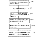
E.リソグラフィツールにおける帯域幅を増大する方法
図3は、リソグラフィツールの制御システムの帯域幅又は作動周波数を増大する方法を示している。ステップ305において、上に説明したように、高い比剛性及び高い熱伝導率を有するチャックが提供される。これらの物理的特性はリソグラフィツールに利点を提供する。上に説明したように、高い比剛性はリソグラフィツールの制御システムにおける増大した帯域幅を許容するのに対し、高い熱伝導率はチャックにおける熱効果の正確な測定を許容する。
E. Method for Increasing Bandwidth in Lithography Tool FIG. 3 illustrates a method for increasing the bandwidth or operating frequency of a lithography tool control system. In
ステップ310においてチャックは機械的に隔離される。例えば、チャックがリソグラフィツールのステージにある場合、チャックは、ステージの他の部分から機械的に隔離されるように、ステージ内において磁気的及び/又は流体静力学的に浮揚されることができる。機械的に隔離することにより、チャックが、機械のより高温又は低温の部分と機械的に接触することによって生ぜしめられる局所的な加熱を受けにくくすることによって、チャックの熱的特性が改善される。さらに重要には、このことは、チャックに伝達される、外部において生ぜしめられる振動の強度を低減する。リソグラフィツールを苦しめる、外部において生ぜしめられる振動の例は、床振動及び音響振動、例えば、近くの高速道路の車両交通、機械の近くを歩行する人間、機械又は建物の中のコンプレッサ、ファン、ブロワ及び同様のものによって生ぜしめられる振動である。
In
ステップ315において、少なくとも1つの有利な寸法におけるチャックの熱膨張が測定される。チャックの高い熱伝導率によりチャックは実質的に等温になる。
In
ステップ320において、高い熱伝導率は、熱膨張の測定から熱ひずみの正確な計算を許容する。低い熱伝導率を有する材料において、局所的な加熱が生じるおそれがあり、熱ひずみを不均一にさせ、熱ひずみの計算の誤りを増加させる。
In
熱ひずみを測定するために、いかなる熱負荷がチャックに提供される前に、チャックの元来の寸法が、熱平衡におけるチャックを用いて測定される。次いで、次元xにおける熱ひずみは、次元xにおける測定された熱膨張を、次元xにおける元来の寸法によって割ったものに等しい。 To measure thermal strain, the original dimensions of the chuck are measured with the chuck in thermal equilibrium before any thermal load is applied to the chuck. The thermal strain in dimension x is then equal to the measured thermal expansion in dimension x divided by the original dimension in dimension x.
ステップ325において、あらゆる残りの次元におけるチャックの熱膨張は、熱ひずみから計算される。例えば、次元yにおける熱膨張は、熱ひずみ(ステップ320において計算されたもの)に、前記のように、次元yにおける元来のチャック寸法を乗じたものに等しい。次元xにおける熱膨張は、次元xにおける測定された熱膨張を、次元xにおける元来の寸法で割ったものに等しい。
In
熱ひずみは、全ての残りの方向のために、計算された熱ひずみの平均に等しいと仮定される。再び、この仮定は、極めて導電性の等方性の材料のためにのみ有効である。チャックにおける熱効果を測定するように適応されることができる、チャック位置を測定するための様々な方法がある。これらの方法の幾つかが上に説明されている。有利な実施形態において、熱膨張を測定するためにエンコーダが使用される。 The thermal strain is assumed to be equal to the calculated average thermal strain for all remaining directions. Again, this assumption is valid only for highly conductive isotropic materials. There are various ways to measure chuck position that can be adapted to measure thermal effects in the chuck. Some of these methods are described above. In an advantageous embodiment, an encoder is used to measure thermal expansion.
ステップ330において、必要ならば、検出されたあらゆる熱膨張のためにチャックの位置が調整される。チャックを位置決めするための様々な方法がこの分野において知られている。
In
上記のステップは、一緒にされると、リソグラフィツールの制御システムにおける増大した帯域幅を許容し、これにより、全体的なリソグラフィ性能、例えば、半導体チップ層内のより小さなフィーチャを製造する能力及び、チップ層の相対的なより正確な位置合わせを改良する。 The above steps, when combined, allow for increased bandwidth in the control system of the lithography tool, thereby providing overall lithographic performance, eg, the ability to produce smaller features in the semiconductor chip layer, and Improve relative more accurate alignment of chip layers.
F.結論
本発明の様々な実施形態が上に説明されたが、これらの実施形態は例として示されているだけであり、限定するものではないことが理解されるべきである。添付の請求項に定義されているような発明の思想及び範囲から逸脱することなく、これらの実施形態の形式及び詳細に様々な変更が加えられてよいことは当業者によって理解されるであろう。したがって、本発明の広さ及び範囲は、上述の典型的な実施形態の何れによっても制限されるべきではなく、添付の請求項及びそれらの請求項の均等物に基づいてのみ定義されるべきである。
F. CONCLUSION While various embodiments of the present invention have been described above, it should be understood that these embodiments are shown by way of example only and not limitation. It will be appreciated by those skilled in the art that various changes can be made in the form and details of these embodiments without departing from the spirit and scope of the invention as defined in the appended claims. . Accordingly, the breadth and scope of the present invention should not be limited by any of the above-described exemplary embodiments, but should be defined only in accordance with the appended claims and their equivalents. is there.
100 装置、 101 レチクルステージ、 102 エンコーダスケール、 104 エンコーダヘッド、 110 チャック、 112 レチクル、 120 第1のレンズグループ、 130 折り返しミラー、140 第2のレンズグループ、 150 ビームスプリッタ、 160 波長板、 170 凹面鏡、 180 第3のレンズグループ、 191 ウェハステージ、 220,220′ エンコーダ、 212,212 トラック、 214,224 エンコーダヘッド、 235 パターニングされた領域 100 apparatus, 101 reticle stage, 102 encoder scale, 104 encoder head, 110 chuck, 112 reticle, 120 first lens group, 130 folding mirror, 140 second lens group, 150 beam splitter, 160 wave plate, 170 concave mirror, 180 third lens group, 191 wafer stage, 220, 220 ′ encoder, 212, 212 track, 214, 224 encoder head, 235 patterned area
Claims (14)
ステージと、
該ステージによって支持されておりかつ、高い比剛性及び高い熱伝導率を有するチャックであって、前記比剛性が約90M(m/s) 2 より高く、前記熱伝導率が、約25W/mKより高く、この場合Wはワット、mはメートル、Kはケルビン温度である、チャックと、
該チャックの熱膨張を少なくとも1つの次元で、該チャック上の互いに反対の縁部にそれぞれ配置された少なくとも2つの位置の変位を比較することにより測定するための手段と、
前記熱膨張に基づき前記チャックの熱ひずみを計算するとともに、該熱ひずみに基づいて別の次元における熱膨張を計算する手段と、
が設けられており、
前記チャックが工作物又は光学素子を支持しており、これにより前記チャックを移動させることにより前記工作物又は前記光学素子も移動するようになっており、
前記熱膨張に基づいて前記チャックの位置を調整する制御システムと、を備えるリソグラフィシステム。 In a lithography system having a control system,
Stage,
A chuck supported by the stage and having high specific rigidity and high thermal conductivity , wherein the specific rigidity is higher than about 90 M (m / s) 2 and the thermal conductivity is higher than about 25 W / mK. High, where W is watts, m is meters, K is Kelvin temperature,
Means for measuring the thermal expansion of the chuck in at least one dimension by comparing displacements of at least two positions respectively located on opposite edges on the chuck;
Means for calculating thermal strain of the chuck based on the thermal expansion, and calculating thermal expansion in another dimension based on the thermal strain;
Is provided,
The chuck supports a workpiece or an optical element, and the workpiece or the optical element is also moved by moving the chuck.
A control system that adjusts a position of the chuck based on the thermal expansion .
前記チャックの第1の縁部及び第2の縁部に沿って位置決めされた線形のトラックの第1の対を有しており、該トラックの第1の対が、リソグラフィツールの定置のフレームに位置決めされたエンコーダヘッドの第1の対に対応しており、前記トラックの第1の対とヘッドの第1の対とが、第1の方向での前記チャックの相対移動の少なくとも2つの独立した測定を生ぜしめるために使用され;
前記チャックの第1の縁部及び第2の縁部に沿って位置決めされた線形のトラックの第2の対を有しており、該トラックの第2の対が、前記定置のフレームに位置決めされたエンコーダヘッドの第2の対に対応しており、前記トラックの第2の対とヘッドの第2の対とが、第1の方向に対して垂直な第2の方向での前記チャックの相対移動の少なくとも2つの独立した測定を生ぜしめるために使用され;
前記チャックの相対移動の前記独立した測定を比較するための手段を有している、請求項7記載のリソグラフィシステム。 The encoder:
A first pair of linear tracks positioned along a first edge and a second edge of the chuck, the first pair of tracks being in a stationary frame of a lithography tool Corresponding to a first pair of positioned encoder heads, wherein the first pair of tracks and the first pair of heads are at least two independent movements of the chuck in a first direction. Used to give rise to measurements;
A second pair of linear tracks positioned along a first edge and a second edge of the chuck, the second pair of tracks positioned on the stationary frame. Corresponding to the second pair of encoder heads, wherein the second pair of tracks and the second pair of heads are relative to each other in the second direction perpendicular to the first direction. Used to produce at least two independent measurements of movement;
A lithographic system according to claim 7 , comprising means for comparing the independent measurements of the relative movement of the chuck.
前記チャックの第1の縁部に位置決めされた第1の線形のエンコーダトラックと、リソグラフィツールの定置のフレームに位置決めされた対応する第1のエンコーダヘッドとを有しており、これにより、前記第1の縁部に対して垂直な方向での前記フレームに対する前記第1のトラックの移動を測定するようになっており;
前記チャックの第2の縁部に位置決めされた第2の線形のエンコーダトラックを有しており、前記第2の縁部が前記第1の縁部に対して平行でかつ該第1の縁部に向き合っており、前記フレームに位置決めされた対応する第2のエンコーダヘッドを有しており、これにより、前記方向での前記フレームに対する前記第2のトラックの移動を測定するようになっており;
前記第1のトラックに対する前記第2のトラックの移動から前記方向での熱膨張が決定される、請求項7記載のリソグラフィシステム。 The encoder:
First linear encoder tracks that are positioned at the first edge portion of the chuck has a first encoder head corresponding positioned on the frame of the stationary lithography tools, thereby, Measuring the movement of the first track relative to the frame in a direction perpendicular to the first edge;
A second linear encoder track positioned at a second edge of the chuck, wherein the second edge is parallel to the first edge and the first edge; And has a corresponding second encoder head positioned on the frame , thereby measuring the movement of the second track relative to the frame in the direction;
The lithographic system of claim 7 , wherein thermal expansion in the direction is determined from movement of the second track relative to the first track.
前記チャックに位置決めされた、第1の端部及び第2の端部を有する線形のエンコーダトラックを有しており;
該エンコーダトラックの前記第1の端部の近傍に、リソグラフィツールの定置のフレームに位置決めされた第1のエンコーダヘッドを有しており、これにより、前記トラックの長さに対して平行な方向での前記フレームに対する前記第1の端部の移動を測定するようになっており;
前記エンコーダトラックの前記第2の端部の近傍に、前記フレームに位置決めされた第2のエンコーダヘッドを有しており、これにより、前記方向での前記フレームに対する前記第2の端部の移動を測定するようになっており;
前記第1の端部に対するエンコーダトラックの前記第2の端部の前記移動から、前記方向での熱膨張が決定されるようになっている、請求項7記載のリソグラフィシステム。 The encoder:
Having a linear encoder track positioned at the chuck and having a first end and a second end;
Proximal to the first end of the encoder track is a first encoder head positioned on a stationary frame of a lithography tool, thereby enabling a direction parallel to the length of the track. Measuring the movement of the first end relative to the frame ;
A second encoder head positioned on the frame in the vicinity of the second end of the encoder track, thereby allowing movement of the second end relative to the frame in the direction; To measure;
The lithographic system of claim 7 , wherein thermal expansion in the direction is determined from the movement of the second end of the encoder track relative to the first end.
リソグラフィツールの定置のフレームに位置決めされた干渉計からの第1の光ビームを反射するための、前記チャックに位置決めされた第1の平坦なミラーを有しており;
前記干渉計からの第2の光ビームを反射するための、前記チャックに位置決めされた、前記第1の平坦なミラーに対して平行でありかつ該第1の平坦なミラーに対して同一平面に位置していない第2の平坦なミラーを有しており;
干渉計によって測定された前記第1のミラーに対する前記第2のミラーの移動から、前記ミラーに対して垂直な方向での熱膨張が決定されるようになっている、請求項11記載のリソグラフィシステム。 Said means for measuring thermal expansion comprises:
A first flat mirror positioned on the chuck for reflecting a first light beam from an interferometer positioned on a stationary frame of the lithography tool;
Parallel to the first flat mirror positioned on the chuck and in the same plane with respect to the first flat mirror for reflecting a second light beam from the interferometer Has a second flat mirror that is not located;
The lithographic system of claim 11 , wherein thermal expansion in a direction perpendicular to the mirror is determined from movement of the second mirror relative to the first mirror measured by an interferometer. .
リソグラフィツールの定置のフレームに位置決めされた干渉計からの第1の光ビームを反射するための、前記チャックの第1の角の近傍に位置決めされた第1の逆反射装置と;
前記干渉計からの第1の光ビームに対して平行な第2のビームを反射するための、前記チャックの第2の角の近傍に位置決めされた第2の逆反射装置とを有しており;
前記干渉計によって測定された前記第1の逆反射装置に対する前記第2の逆反射装置の移動から、前記ビームに対して平行な方向での熱膨張が決定されるようになっている、請求項11記載のリソグラフィシステム。 Said means for measuring thermal expansion comprises:
A first retroreflective device positioned proximate a first corner of the chuck for reflecting a first light beam from an interferometer positioned on a stationary frame of the lithography tool;
A second retro-reflecting device positioned in the vicinity of the second corner of the chuck for reflecting a second beam parallel to the first light beam from the interferometer. ;
The thermal expansion in a direction parallel to the beam is determined from the movement of the second retroreflective device relative to the first retroreflective device measured by the interferometer. The lithography system according to 11 .
前記チャックの第1の側に沿って位置決めされた第1の平坦なストリップと、第1のセンサヘッドとを有しており、該第1のセンサヘッドが、該第1のセンサヘッドと前記第1のストリップとの間の距離を測定するためにリソグラフィツールの定置のフレームに位置決めされており;
前記第1の側に対して平行でかつ該第1の側に向き合った、前記チャックの第2の側に沿って位置決めされた第2の平坦なストリップと、第2のセンサヘッドとを有しており、該第2のセンサヘッドが、該第2のセンサヘッドと前記第2のストリップとの間の距離を測定するために前記フレームに位置決めされており;
前記第1のストリップに対する前記第2のストリップの移動から、前記ストリップに対して垂直な方向での熱膨張が決定されるようになっている、請求項1乃至請求項6のいずれか一項記載のリソグラフィシステム。 Said means for measuring thermal expansion comprises:
A first flat strip positioned along a first side of the chuck; and a first sensor head, the first sensor head including the first sensor head and the first sensor head. Positioned on a stationary frame of a lithography tool for measuring the distance between one strip;
A second flat strip positioned along the second side of the chuck and parallel to the first side and facing the first side; and a second sensor head. The second sensor head is positioned on the frame to measure a distance between the second sensor head and the second strip;
From movement of the second strip to said first strip, so that the thermal expansion in the direction perpendicular are determined for the strip, according to any one of claims 1 to claim 6 Lithographic system .
Applications Claiming Priority (2)
| Application Number | Priority Date | Filing Date | Title |
|---|---|---|---|
| US10/448,027 US7025498B2 (en) | 2003-05-30 | 2003-05-30 | System and method of measuring thermal expansion |
| US10/448027 | 2003-05-30 |
Related Parent Applications (1)
| Application Number | Title | Priority Date | Filing Date |
|---|---|---|---|
| JP2004162319A Division JP4610231B2 (en) | 2003-05-30 | 2004-05-31 | Stage with thermal expansion compensation |
Publications (2)
| Publication Number | Publication Date |
|---|---|
| JP2009010393A JP2009010393A (en) | 2009-01-15 |
| JP4986942B2 true JP4986942B2 (en) | 2012-07-25 |
Family
ID=33451401
Family Applications (2)
| Application Number | Title | Priority Date | Filing Date |
|---|---|---|---|
| JP2004162319A Expired - Fee Related JP4610231B2 (en) | 2003-05-30 | 2004-05-31 | Stage with thermal expansion compensation |
| JP2008179652A Expired - Fee Related JP4986942B2 (en) | 2003-05-30 | 2008-07-10 | Lithography system |
Family Applications Before (1)
| Application Number | Title | Priority Date | Filing Date |
|---|---|---|---|
| JP2004162319A Expired - Fee Related JP4610231B2 (en) | 2003-05-30 | 2004-05-31 | Stage with thermal expansion compensation |
Country Status (2)
| Country | Link |
|---|---|
| US (1) | US7025498B2 (en) |
| JP (2) | JP4610231B2 (en) |
Families Citing this family (62)
| Publication number | Priority date | Publication date | Assignee | Title |
|---|---|---|---|---|
| DE102004003784B4 (en) * | 2004-01-23 | 2011-01-13 | Ormecon Gmbh | Dispersion of intrinsically conductive polyaniline and their use |
| JP4756984B2 (en) * | 2005-10-07 | 2011-08-24 | キヤノン株式会社 | Exposure apparatus, exposure apparatus control method, and device manufacturing method |
| US20070139855A1 (en) * | 2005-12-21 | 2007-06-21 | Asml Netherlands B.V. | Lithographic apparatus and method of manufacturing an electrostatic clamp for a lithographic apparatus |
| TWI550688B (en) * | 2006-01-19 | 2016-09-21 | 尼康股份有限公司 | Liquid immersion exposure device, liquid immersion exposure method, and component manufacturing method |
| KR101495471B1 (en) * | 2006-02-21 | 2015-02-23 | 가부시키가이샤 니콘 | Pattern forming apparatus, mark detecting apparatus, exposure apparatus, pattern forming method, exposure method and device manufacturing method |
| US8027021B2 (en) | 2006-02-21 | 2011-09-27 | Nikon Corporation | Measuring apparatus and method, processing apparatus and method, pattern forming apparatus and method, exposure apparatus and method, and device manufacturing method |
| EP2003680B1 (en) | 2006-02-21 | 2013-05-29 | Nikon Corporation | Exposure apparatus, exposure method and device manufacturing method |
| US7593096B2 (en) * | 2006-05-15 | 2009-09-22 | Asml Netherlands B.V. | Lithographic apparatus and device manufacturing method |
| EP3064999B1 (en) | 2006-08-31 | 2017-07-26 | Nikon Corporation | Exposure apparatus, exposure method, and device manufacturing method |
| TWI609252B (en) * | 2006-08-31 | 2017-12-21 | Nikon Corp | Moving body driving system and moving body driving method, pattern forming apparatus and method, exposure apparatus and method, element manufacturing method, and determination method |
| SG182983A1 (en) * | 2006-08-31 | 2012-08-30 | Nikon Corp | Movable body drive method and movable body drive system, pattern formation method and apparatus, exposure method and apparatus, and device manufacturing method |
| TWI596656B (en) | 2006-09-01 | 2017-08-21 | 尼康股份有限公司 | Moving body driving method and moving body driving system, pattern forming method and apparatus, exposure method and apparatus, element manufacturing method, and correction method |
| KR101604564B1 (en) | 2006-09-01 | 2016-03-17 | 가부시키가이샤 니콘 | Mobile body driving method, mobile body driving system, pattern forming method and apparatus, exposure method and apparatus and device manufacturing method |
| EP2068112A4 (en) * | 2006-09-29 | 2017-11-15 | Nikon Corporation | Mobile unit system, pattern forming device, exposing device, exposing method, and device manufacturing method |
| US9440812B2 (en) | 2007-01-11 | 2016-09-13 | 3M Innovative Properties Company | Web longitudinal position sensor |
| US7678458B2 (en) | 2007-01-24 | 2010-03-16 | Asml Holding N.V. | Bonding silicon silicon carbide to glass ceramics |
| US8760615B2 (en) | 2007-05-24 | 2014-06-24 | Asml Netherlands B.V. | Lithographic apparatus having encoder type position sensor system |
| US8687166B2 (en) * | 2007-05-24 | 2014-04-01 | Asml Netherlands B.V. | Lithographic apparatus having an encoder position sensor system |
| CN101688794B (en) | 2007-06-19 | 2012-12-12 | 3M创新有限公司 | Systems and methods for fabricating displacement scales |
| WO2008157619A2 (en) * | 2007-06-19 | 2008-12-24 | 3M Innovative Properties Company | Total internal reflection displacement scale |
| CN101678977B (en) | 2007-06-19 | 2012-07-11 | 3M创新有限公司 | Systems and methods for indicating the position of a web |
| JP5489068B2 (en) * | 2007-07-24 | 2014-05-14 | 株式会社ニコン | POSITION MEASUREMENT SYSTEM, EXPOSURE APPARATUS, POSITION MEASUREMENT METHOD, EXPOSURE METHOD, DEVICE MANUFACTURING METHOD, TOOL AND MEASUREMENT METHOD |
| US8237919B2 (en) * | 2007-08-24 | 2012-08-07 | Nikon Corporation | Movable body drive method and movable body drive system, pattern formation method and apparatus, exposure method and apparatus, and device manufacturing method for continuous position measurement of movable body before and after switching between sensor heads |
| US20090100814A1 (en) * | 2007-10-22 | 2009-04-23 | Philip Egging | Non-Powered Roller for Assisting Crop Pick-Up With a Baler |
| US9013681B2 (en) * | 2007-11-06 | 2015-04-21 | Nikon Corporation | Movable body apparatus, pattern formation apparatus and exposure apparatus, and device manufacturing method |
| US9256140B2 (en) * | 2007-11-07 | 2016-02-09 | Nikon Corporation | Movable body apparatus, pattern formation apparatus and exposure apparatus, and device manufacturing method with measurement device to measure movable body in Z direction |
| US8665455B2 (en) * | 2007-11-08 | 2014-03-04 | Nikon Corporation | Movable body apparatus, pattern formation apparatus and exposure apparatus, and device manufacturing method |
| US8422015B2 (en) * | 2007-11-09 | 2013-04-16 | Nikon Corporation | Movable body apparatus, pattern formation apparatus and exposure apparatus, and device manufacturing method |
| NL1036180A1 (en) * | 2007-11-20 | 2009-05-25 | Asml Netherlands Bv | Stage system, lithographic apparatus including such stage system, and correction method. |
| US8115906B2 (en) * | 2007-12-14 | 2012-02-14 | Nikon Corporation | Movable body system, pattern formation apparatus, exposure apparatus and measurement device, and device manufacturing method |
| US8711327B2 (en) * | 2007-12-14 | 2014-04-29 | Nikon Corporation | Exposure apparatus, exposure method, and device manufacturing method |
| EP2284865B1 (en) | 2008-04-30 | 2015-09-02 | Nikon Corporation | Stage apparatus, patterning apparatus, exposure apparatus, stage drive apparatus, exposure method, and device fabrication method |
| US8817236B2 (en) | 2008-05-13 | 2014-08-26 | Nikon Corporation | Movable body system, movable body drive method, pattern formation apparatus, pattern formation method, exposure apparatus, exposure method, and device manufacturing method |
| US8228482B2 (en) * | 2008-05-13 | 2012-07-24 | Nikon Corporation | Exposure apparatus, exposure method, and device manufacturing method |
| US8786829B2 (en) * | 2008-05-13 | 2014-07-22 | Nikon Corporation | Exposure apparatus, exposure method, and device manufacturing method |
| NL2003039A1 (en) * | 2008-07-22 | 2010-01-25 | Asml Netherlands Bv | Lithographic apparatus and device manufacturing method. |
| US8186875B2 (en) * | 2008-09-14 | 2012-05-29 | Nuovo Pignone S.P.A. | Method for determining reheat cracking susceptibility |
| US8599359B2 (en) | 2008-12-19 | 2013-12-03 | Nikon Corporation | Exposure apparatus, exposure method, device manufacturing method, and carrier method |
| US8773635B2 (en) * | 2008-12-19 | 2014-07-08 | Nikon Corporation | Exposure apparatus, exposure method, and device manufacturing method |
| US8760629B2 (en) | 2008-12-19 | 2014-06-24 | Nikon Corporation | Exposure apparatus including positional measurement system of movable body, exposure method of exposing object including measuring positional information of movable body, and device manufacturing method that includes exposure method of exposing object, including measuring positional information of movable body |
| US8902402B2 (en) * | 2008-12-19 | 2014-12-02 | Nikon Corporation | Movable body apparatus, exposure apparatus, exposure method, and device manufacturing method |
| EP2380067B1 (en) | 2008-12-29 | 2019-06-26 | 3M Innovative Properties Company | Method and system for determining a longitudinal position of an elongated web |
| JP5580337B2 (en) | 2008-12-30 | 2014-08-27 | スリーエム イノベイティブ プロパティズ カンパニー | Apparatus for creating a reference on a substrate |
| US8334983B2 (en) * | 2009-05-22 | 2012-12-18 | Asml Netherlands B.V. | Lithographic apparatus and device manufacturing method |
| KR101670640B1 (en) * | 2009-08-07 | 2016-10-28 | 가부시키가이샤 니콘 | Moving body apparatus, exposure apparatus, exposure method, and device manufacturing method |
| US8514395B2 (en) | 2009-08-25 | 2013-08-20 | Nikon Corporation | Exposure method, exposure apparatus, and device manufacturing method |
| US8488109B2 (en) | 2009-08-25 | 2013-07-16 | Nikon Corporation | Exposure method, exposure apparatus, and device manufacturing method |
| US8493547B2 (en) | 2009-08-25 | 2013-07-23 | Nikon Corporation | Exposure apparatus, exposure method, and device manufacturing method |
| US20110096318A1 (en) * | 2009-09-28 | 2011-04-28 | Nikon Corporation | Exposure apparatus and device fabricating method |
| US20110096306A1 (en) * | 2009-09-28 | 2011-04-28 | Nikon Corporation | Stage apparatus, exposure apparatus, driving method, exposing method, and device fabricating method |
| US20110096312A1 (en) * | 2009-09-28 | 2011-04-28 | Nikon Corporation | Exposure apparatus and device fabricating method |
| US20110102761A1 (en) * | 2009-09-28 | 2011-05-05 | Nikon Corporation | Stage apparatus, exposure apparatus, and device fabricating method |
| US20110123913A1 (en) * | 2009-11-19 | 2011-05-26 | Nikon Corporation | Exposure apparatus, exposing method, and device fabricating method |
| US20110128523A1 (en) * | 2009-11-19 | 2011-06-02 | Nikon Corporation | Stage apparatus, exposure apparatus, driving method, exposing method, and device fabricating method |
| US8488106B2 (en) * | 2009-12-28 | 2013-07-16 | Nikon Corporation | Movable body drive method, movable body apparatus, exposure method, exposure apparatus, and device manufacturing method |
| JP2012089768A (en) * | 2010-10-22 | 2012-05-10 | Nikon Corp | Exposure device and device manufacturing method |
| TWI467126B (en) * | 2011-11-09 | 2015-01-01 | Zygo Corp | Thermally stable optical sensor mount |
| US9207549B2 (en) | 2011-12-29 | 2015-12-08 | Nikon Corporation | Exposure apparatus and exposure method, and device manufacturing method with encoder of higher reliability for position measurement |
| US9377700B2 (en) * | 2012-06-01 | 2016-06-28 | Asml Holding N.V. | Determining position and curvature information directly from a surface of a patterning device |
| JP6381184B2 (en) * | 2013-07-09 | 2018-08-29 | キヤノン株式会社 | Calibration method, measuring apparatus, exposure apparatus, and article manufacturing method |
| CN106813718B (en) * | 2017-03-01 | 2019-04-12 | 西安交通大学 | A kind of device and method measuring thin film strain and thermal conductivity |
| WO2018188828A1 (en) | 2017-04-11 | 2018-10-18 | Asml Netherlands B.V. | Lithographic apparatus and cooling method |
Family Cites Families (60)
| Publication number | Priority date | Publication date | Assignee | Title |
|---|---|---|---|---|
| US3788746A (en) * | 1972-10-02 | 1974-01-29 | Hewlett Packard Co | Optical dilatometer |
| JPS53145475A (en) * | 1977-05-24 | 1978-12-18 | Toshiba Corp | Position detector |
| US4334778A (en) * | 1980-09-12 | 1982-06-15 | The United States Of America As Represented By The United States Department Of Energy | Dual surface interferometer |
| KR910004158B1 (en) * | 1983-08-15 | 1991-06-22 | Sinagawa Sirotenga Co Ltd | Thermal deformation measuring system of ceranics and the like |
| US5350899A (en) * | 1992-04-15 | 1994-09-27 | Hiroichi Ishikawa | Semiconductor wafer temperature determination by optical measurement of wafer expansion in processing apparatus chamber |
| US4930894A (en) * | 1984-04-27 | 1990-06-05 | Hewlett-Packard Company | Minimum deadpath interferometer and dilatometer |
| US4711574A (en) * | 1984-04-27 | 1987-12-08 | Hewlett-Packard Company | Minimum deadpath interferometer and dilatometer |
| JPH0674963B2 (en) * | 1988-02-08 | 1994-09-21 | 株式会社日立製作所 | Laser interferometer and positioning method using the same |
| US5064289A (en) * | 1989-02-23 | 1991-11-12 | Hewlett-Packard Company | Linear-and-angular measuring plane mirror interferometer |
| US5754403A (en) * | 1989-09-29 | 1998-05-19 | Texas Instruments Incorporated | Constraining core for surface mount technology |
| US5298970A (en) * | 1990-03-20 | 1994-03-29 | Kabushiki Kaisha Kobe Seiko Sho | Sample evaluating method by using thermal expansion displacement |
| JP3077176B2 (en) * | 1990-08-13 | 2000-08-14 | 株式会社ニコン | Exposure method, apparatus, and element manufacturing method |
| USH1370H (en) * | 1991-04-15 | 1994-11-01 | The United States Of America As Represented By The Secretary Of The Navy | Interferometric vibration and thermal expansion compensator |
| US5220405A (en) * | 1991-12-20 | 1993-06-15 | International Business Machines Corporation | Interferometer for in situ measurement of thin film thickness changes |
| US5645351A (en) * | 1992-05-20 | 1997-07-08 | Hitachi, Ltd. | Temperature measuring method using thermal expansion and an apparatus for carrying out the same |
| JPH0613299A (en) * | 1992-06-25 | 1994-01-21 | Hitachi Ltd | Electron beam lithography method and its lithography equipment |
| JPH0636997A (en) * | 1992-07-15 | 1994-02-10 | Hitachi Ltd | Electron beam lithography apparatus |
| US6005333A (en) * | 1993-05-05 | 1999-12-21 | Canon Kabushiki Kaisha | Electron beam-generating device, and image-forming apparatus and recording apparatus employing the same |
| JP3600881B2 (en) * | 1993-12-27 | 2004-12-15 | 株式会社ニコン | Interferometer and stage device |
| ATE155238T1 (en) * | 1994-02-26 | 1997-07-15 | Heidenhain Gmbh Dr Johannes | INTERFEROMETER |
| US5555089A (en) * | 1994-11-30 | 1996-09-10 | Anvik Corporation | Absolute distance measuring interferometry using multi-pass resonant cavity referenced to a stabilized laser source |
| JPH098103A (en) * | 1995-06-19 | 1997-01-10 | Nikon Corp | Projection exposing device and method thereof |
| DE69709584T2 (en) * | 1996-03-04 | 2002-06-13 | Asm Lithography Bv | LITHOGRAPHIC DEVICE FOR STEP-AND-SCAN TRANSFER OF A MASK PATTERN |
| KR100525521B1 (en) * | 1996-10-21 | 2006-01-27 | 가부시키가이샤 니콘 | Exposure apparatus and exposure method |
| US5944097A (en) * | 1997-05-06 | 1999-08-31 | Northrop Grumman Corporation | Composite substrate carrier for high power electronic devices |
| US6057921A (en) * | 1997-07-08 | 2000-05-02 | Etec Systems, Inc. | Two piece mirror arrangement for interferometrically controlled stage |
| US6672759B2 (en) * | 1997-07-11 | 2004-01-06 | International Business Machines Corporation | Method for accounting for clamp expansion in a coefficient of thermal expansion measurement |
| US6522386B1 (en) * | 1997-07-24 | 2003-02-18 | Nikon Corporation | Exposure apparatus having projection optical system with aberration correction element |
| JPH1187228A (en) * | 1997-09-01 | 1999-03-30 | Nikon Corp | Aligner and method of exposure |
| JP2956671B2 (en) * | 1997-11-25 | 1999-10-04 | 日本電気株式会社 | Reticle inspection method and inspection device |
| US6020964A (en) * | 1997-12-02 | 2000-02-01 | Asm Lithography B.V. | Interferometer system and lithograph apparatus including an interferometer system |
| JP2963890B2 (en) * | 1998-03-09 | 1999-10-18 | 株式会社スーパーシリコン研究所 | Wafer optical shape measuring instrument |
| JPH11295031A (en) * | 1998-04-08 | 1999-10-29 | Canon Inc | Positioning stage device, method for measuring its position, exposure device with positioning stage device, and method for manufacturing device |
| JP3810039B2 (en) * | 1998-05-06 | 2006-08-16 | キヤノン株式会社 | Stage equipment |
| JP3720582B2 (en) * | 1998-06-04 | 2005-11-30 | キヤノン株式会社 | Projection exposure apparatus and projection exposure method |
| JP2000049066A (en) * | 1998-07-27 | 2000-02-18 | Canon Inc | Aligner and manufacture of devices |
| DE19858428C2 (en) * | 1998-12-17 | 2002-09-12 | Leica Microsystems | Coordinate-measuring arrangement |
| JP2000252352A (en) * | 1999-03-03 | 2000-09-14 | Nikon Corp | Substrate holder and charged particle beam aligner employing it |
| TW490596B (en) * | 1999-03-08 | 2002-06-11 | Asm Lithography Bv | Lithographic projection apparatus, method of manufacturing a device using the lithographic projection apparatus, device manufactured according to the method and method of calibrating the lithographic projection apparatus |
| EP1077393A2 (en) * | 1999-08-19 | 2001-02-21 | Canon Kabushiki Kaisha | Substrate attracting and holding system for use in exposure apparatus |
| JP2001160530A (en) * | 1999-12-01 | 2001-06-12 | Nikon Corp | Stage system and exposure device |
| JP2001168000A (en) * | 1999-12-03 | 2001-06-22 | Nikon Corp | Method for manufacturing aligner and method for manufacturing micro-device using the aligner manufactured by the manufacturing method |
| US6406991B2 (en) * | 1999-12-27 | 2002-06-18 | Hoya Corporation | Method of manufacturing a contact element and a multi-layered wiring substrate, and wafer batch contact board |
| US6704089B2 (en) * | 2000-04-28 | 2004-03-09 | Asml Netherlands B.V. | Lithographic projection apparatus, a method for determining a position of a substrate alignment mark, a device manufacturing method and device manufactured thereby |
| WO2002003025A1 (en) * | 2000-06-30 | 2002-01-10 | Unova Ip Corp. | Method for determining effective coefficient of thermal expansion |
| US7289212B2 (en) * | 2000-08-24 | 2007-10-30 | Asml Netherlands B.V. | Lithographic apparatus, device manufacturing method and device manufacturing thereby |
| US6653639B1 (en) * | 2000-10-17 | 2003-11-25 | Nikon Corporation | Chuck for mounting reticle to a reticle stage |
| KR100579603B1 (en) * | 2001-01-15 | 2006-05-12 | 에이에스엠엘 네델란즈 비.브이. | Lithographic Apparatus |
| JP2002231611A (en) * | 2001-02-02 | 2002-08-16 | Nikon Corp | Aligner and method of manufacturing device |
| JP3762307B2 (en) * | 2001-02-15 | 2006-04-05 | キヤノン株式会社 | Exposure apparatus including laser interferometer system |
| JP2003057419A (en) * | 2001-08-21 | 2003-02-26 | Canon Inc | Optical reflection mirror, method for manufacturing optical reflection mirror, positioning device and method for manufacturing semiconductor device |
| WO2003019112A1 (en) * | 2001-08-23 | 2003-03-06 | Zygo Corporation | Optical interferometry |
| ITMO20010248A1 (en) * | 2001-12-12 | 2003-06-12 | Expert System Solutions Srl | PERFECTED OPTICAL DILATOMETER |
| US6734117B2 (en) * | 2002-03-12 | 2004-05-11 | Nikon Corporation | Periodic clamping method and apparatus to reduce thermal stress in a wafer |
| JP4006251B2 (en) * | 2002-03-20 | 2007-11-14 | キヤノン株式会社 | Mirror device, mirror adjustment method, exposure apparatus, exposure method, and semiconductor device manufacturing method |
| CN100476599C (en) * | 2002-09-20 | 2009-04-08 | Asml荷兰有限公司 | Photoetching mark structure, photoetching projection device comprising the photoetching mark structure, and method for aligning with the photoetching mark structure |
| US6654660B1 (en) * | 2002-11-04 | 2003-11-25 | Advanced Micro Devices, Inc. | Controlling thermal expansion of mask substrates by scatterometry |
| US20040145751A1 (en) * | 2003-01-28 | 2004-07-29 | Binnard Michael B. | Square wafer chuck with mirror |
| JP4164414B2 (en) * | 2003-06-19 | 2008-10-15 | キヤノン株式会社 | Stage equipment |
| US6939036B2 (en) * | 2003-11-04 | 2005-09-06 | Certainteed Corporation | Temperature-expansion indicator for siding panels |
-
2003
- 2003-05-30 US US10/448,027 patent/US7025498B2/en not_active Expired - Lifetime
-
2004
- 2004-05-31 JP JP2004162319A patent/JP4610231B2/en not_active Expired - Fee Related
-
2008
- 2008-07-10 JP JP2008179652A patent/JP4986942B2/en not_active Expired - Fee Related
Also Published As
| Publication number | Publication date |
|---|---|
| US20040240513A1 (en) | 2004-12-02 |
| JP2009010393A (en) | 2009-01-15 |
| US7025498B2 (en) | 2006-04-11 |
| JP2005045215A (en) | 2005-02-17 |
| JP4610231B2 (en) | 2011-01-12 |
Similar Documents
| Publication | Publication Date | Title |
|---|---|---|
| JP4986942B2 (en) | Lithography system | |
| US11385557B2 (en) | Measurement device, lithography system and exposure apparatus, and device manufacturing method | |
| US6864988B2 (en) | Optical system with isolated measuring structure | |
| KR101619280B1 (en) | Projection system and lithographic apparatus | |
| JP7220176B2 (en) | Substrate processing system, substrate processing method, and device manufacturing method | |
| US9477092B2 (en) | Optical imaging arrangement with individually actively supported components | |
| Holmes et al. | The long-range scanning stage: a novel platform for scanned-probe microscopy | |
| US20180046096A1 (en) | Measurement device, lithography system and exposure apparatus, and control method, overlay measurement method and device manufacturing method | |
| US9229340B2 (en) | Lithographic apparatus | |
| JP2000049066A (en) | Aligner and manufacture of devices | |
| JP2012028797A (en) | Lithographic apparatus and device manufacturing method | |
| JPWO2018038071A1 (en) | Measurement system, substrate processing system, and device manufacturing method | |
| JP2006140366A (en) | Projection optical system and exposure device | |
| JP4113168B2 (en) | Foam core chuck for scanning stage of lithography system | |
| JP4424739B2 (en) | Stage equipment | |
| US20080100930A1 (en) | Optical measuring system, and a projection objective | |
| JP2001135561A (en) | Stage system, aligner and method of fabrication for device | |
| JP2004241670A (en) | Assembly structure, stage apparatus, and aligner | |
| US20240134295A1 (en) | Substrate processing system and substrate processing method, and device manufacturing method | |
| JP4120361B2 (en) | Measuring device, stage device, and measuring method | |
| JPWO2010143652A1 (en) | Exposure method and apparatus, and device manufacturing method | |
| JPH11221732A (en) | Stage device and machining device |
Legal Events
| Date | Code | Title | Description |
|---|---|---|---|
| A131 | Notification of reasons for refusal |
Free format text: JAPANESE INTERMEDIATE CODE: A131 Effective date: 20110422 |
|
| A521 | Request for written amendment filed |
Free format text: JAPANESE INTERMEDIATE CODE: A523 Effective date: 20110714 |
|
| TRDD | Decision of grant or rejection written | ||
| A01 | Written decision to grant a patent or to grant a registration (utility model) |
Free format text: JAPANESE INTERMEDIATE CODE: A01 Effective date: 20120327 |
|
| A01 | Written decision to grant a patent or to grant a registration (utility model) |
Free format text: JAPANESE INTERMEDIATE CODE: A01 |
|
| A61 | First payment of annual fees (during grant procedure) |
Free format text: JAPANESE INTERMEDIATE CODE: A61 Effective date: 20120424 |
|
| R150 | Certificate of patent or registration of utility model |
Free format text: JAPANESE INTERMEDIATE CODE: R150 Ref document number: 4986942 Country of ref document: JP Free format text: JAPANESE INTERMEDIATE CODE: R150 |
|
| FPAY | Renewal fee payment (event date is renewal date of database) |
Free format text: PAYMENT UNTIL: 20150511 Year of fee payment: 3 |
|
| R250 | Receipt of annual fees |
Free format text: JAPANESE INTERMEDIATE CODE: R250 |
|
| R250 | Receipt of annual fees |
Free format text: JAPANESE INTERMEDIATE CODE: R250 |
|
| R250 | Receipt of annual fees |
Free format text: JAPANESE INTERMEDIATE CODE: R250 |
|
| R250 | Receipt of annual fees |
Free format text: JAPANESE INTERMEDIATE CODE: R250 |
|
| R250 | Receipt of annual fees |
Free format text: JAPANESE INTERMEDIATE CODE: R250 |
|
| R250 | Receipt of annual fees |
Free format text: JAPANESE INTERMEDIATE CODE: R250 |
|
| R250 | Receipt of annual fees |
Free format text: JAPANESE INTERMEDIATE CODE: R250 |
|
| LAPS | Cancellation because of no payment of annual fees |