JP4976094B2 - Illumination optical apparatus, exposure apparatus, exposure method, and microdevice manufacturing method - Google Patents
Illumination optical apparatus, exposure apparatus, exposure method, and microdevice manufacturing method Download PDFInfo
- Publication number
- JP4976094B2 JP4976094B2 JP2006262589A JP2006262589A JP4976094B2 JP 4976094 B2 JP4976094 B2 JP 4976094B2 JP 2006262589 A JP2006262589 A JP 2006262589A JP 2006262589 A JP2006262589 A JP 2006262589A JP 4976094 B2 JP4976094 B2 JP 4976094B2
- Authority
- JP
- Japan
- Prior art keywords
- light
- light beam
- polarization state
- polarization
- illumination optical
- Prior art date
- Legal status (The legal status is an assumption and is not a legal conclusion. Google has not performed a legal analysis and makes no representation as to the accuracy of the status listed.)
- Active
Links
Images


Description
本発明は、照明光学装置、露光装置、露光方法、およびマイクロデバイスの製造方法に関し、特に半導体素子、撮像素子、液晶表示素子、薄膜磁気ヘッド等のマイクロデバイスをリソグラフィー工程で製造する際に使用される露光装置に好適な照明光学装置に関するものである。 The present invention relates to an illumination optical apparatus, an exposure apparatus, an exposure method, and a microdevice manufacturing method, and is particularly used when a microdevice such as a semiconductor element, an image sensor, a liquid crystal display element, or a thin film magnetic head is manufactured in a lithography process. The present invention relates to an illumination optical apparatus suitable for an exposure apparatus.
この種の典型的な露光装置においては、光源から射出された光束が、オプティカルインテグレータとしてのフライアイレンズを介して、多数の光源からなる実質的な面光源としての二次光源を形成する。二次光源(一般には、照明光学装置の照明瞳またはその近傍に形成される照明瞳分布)からの光束は、フライアイレンズの後側焦点面の近傍に配置された開口絞りを介して制限された後、コンデンサーレンズに入射する。 In a typical exposure apparatus of this type, a light beam emitted from a light source forms a secondary light source as a substantial surface light source including a large number of light sources via a fly-eye lens as an optical integrator. The light flux from the secondary light source (generally, the illumination pupil distribution formed in or near the illumination pupil of the illumination optical device) is limited through an aperture stop disposed in the vicinity of the rear focal plane of the fly-eye lens. After that, it enters the condenser lens.
コンデンサーレンズにより集光された光束は、所定のパターンが形成されたマスクを重畳的に照明する。マスクのパターンを透過した光は、投影光学系を介してウェハ上に結像する。こうして、ウェハ上には、マスクパターンが投影露光(転写)される。なお、マスクに形成されたパターンは高集積化されており、この微細パターンをウェハ上に正確に転写するにはウェハ上において均一な照度分布を得ることが不可欠である。 The light beam condensed by the condenser lens illuminates the mask on which a predetermined pattern is formed in a superimposed manner. The light transmitted through the mask pattern forms an image on the wafer via the projection optical system. Thus, the mask pattern is projected and exposed (transferred) onto the wafer. The pattern formed on the mask is highly integrated, and it is essential to obtain a uniform illuminance distribution on the wafer in order to accurately transfer this fine pattern onto the wafer.
たとえば本出願人の出願にかかる特許第3246615号公報には、任意方向の微細パターンを忠実に転写するのに適した照明条件を実現するために、フライアイレンズの後側焦点面に輪帯状の二次光源を形成し、この輪帯状の二次光源を通過する光束がその周方向を偏光方向とする直線偏光状態(以下、略して「周方向偏光状態」という)になるように設定する技術が開示されている。 For example, in Japanese Patent No. 3246615 relating to the application of the present applicant, in order to realize an illumination condition suitable for faithfully transferring a fine pattern in an arbitrary direction, an annular zone is formed on the rear focal plane of the fly-eye lens. A technology for forming a secondary light source and setting the light beam passing through the annular secondary light source to be in a linear polarization state (hereinafter referred to as “circumferential polarization state” for short) with the circumferential direction as the polarization direction. Is disclosed.
しかしながら、上述の公報に開示された従来技術では、フライアイレンズを介して形成された円形状の光束を輪帯状の開口部を有する開口絞りを介して制限することにより輪帯状の二次光源を形成している。その結果、従来技術では、開口絞りにおいて大きな光量損失が発生し、ひいては露光装置のスループットが低下するという不都合があった。 However, in the prior art disclosed in the above publication, the annular light source is limited by restricting the circular light beam formed through the fly-eye lens through an aperture stop having an annular opening. Forming. As a result, the prior art has a disadvantage in that a large light loss occurs in the aperture stop, which in turn reduces the throughput of the exposure apparatus.
本発明は、前述の課題に鑑みてなされたものであり、光量損失を良好に抑えつつ、周方向偏光状態の輪帯状の照明瞳分布を形成することを目的とする。また、本発明は、光量損失を良好に抑えつつ周方向偏光状態の輪帯状の照明瞳分布を形成することによって、適切な照明条件のもとで任意方向の微細パターンを忠実に且つ高スループットで転写することを目的とする。 The present invention has been made in view of the above-described problems, and an object of the present invention is to form a ring-shaped illumination pupil distribution in a circumferentially polarized state while favorably suppressing a light amount loss. In addition, the present invention forms a ring-shaped illumination pupil distribution in a circumferentially polarized state while suppressing loss of light quantity satisfactorily, so that a fine pattern in an arbitrary direction can be faithfully and high-throughput under appropriate illumination conditions. The purpose is to transfer.
前記課題を解決するために、本発明の第1形態では、光源からの光束に基づいて被照射面を照明する照明光学装置において、
入射する光の偏光状態を切り換える偏光状態切換手段と、
前記偏光状態切換手段と前記被照射面との間の光路に配置されて、入射光束に基づいて所定面に所定の偏光特性を持つ光強度分布を形成するための光束変換素子とを備え、
前記光束変換素子は、旋光性を有する光学材料により形成されて、前記入射光束に基づいて前記所定の偏光特性を持つ光強度分布のうちの第1領域分布にて第1偏光状態を形成するための第1基本素子と、旋光性を有する光学材料により形成されて、前記入射光束に基づいて前記所定の偏光特性を持つ光強度分布のうちの第2領域分布にて第2偏光状態を形成するための第2基本素子とを備え、
前記第1基本素子と前記第2基本素子とは、光の透過方向に沿った厚さが互いに異なることを特徴とする照明光学装置を提供する。
In order to solve the above problems, in the first embodiment of the present invention, in the illumination optical device that illuminates the irradiated surface based on the light flux from the light source,
Polarization state switching means for switching the polarization state of incident light;
A light beam conversion element that is disposed in an optical path between the polarization state switching unit and the irradiated surface and that forms a light intensity distribution having a predetermined polarization characteristic on a predetermined surface based on an incident light beam;
The light beam conversion element is formed of an optical material having optical rotation, and forms a first polarization state in a first region distribution of the light intensity distribution having the predetermined polarization characteristic based on the incident light beam. The second polarization state is formed by the second region distribution of the light intensity distribution having the predetermined polarization characteristics based on the incident light flux. A second basic element for
The first basic element and the second basic element are different from each other in thickness along the light transmission direction.
本発明の第2形態では、マスクを照明するための第1形態の照明光学装置を備え、前記マスクのパターンを感光性基板上に露光することを特徴とする露光装置を提供する。 According to a second aspect of the present invention, there is provided an exposure apparatus comprising the illumination optical apparatus according to the first aspect for illuminating a mask, and exposing the pattern of the mask onto a photosensitive substrate.
本発明の第3形態では、第1形態の照明光学装置を用いてマスクを照明する照明工程と、前記マスクのパターンを感光性基板上に露光する露光工程とを含むことを特徴とする露光方法を提供する。 According to a third aspect of the present invention, there is provided an exposure method comprising: an illuminating step of illuminating a mask using the illumination optical apparatus according to the first aspect; and an exposing step of exposing a pattern of the mask onto a photosensitive substrate. I will provide a.
本発明の第4形態では、第1形態の照明光学装置を用いてマスクを照明する照明工程と、前記マスクのパターンを感光性基板上に露光する露光工程とを含むことを特徴とするマイクロデバイスの製造方法を提供する。 According to a fourth aspect of the present invention, there is provided a microdevice comprising: an illuminating step of illuminating a mask using the illumination optical apparatus according to the first aspect; and an exposing step of exposing a pattern of the mask onto a photosensitive substrate. A manufacturing method is provided.
本発明の照明光学装置では、光束変換素子の作用により、光量損失を実質的に発生させることなく、周方向偏光状態の輪帯状の照明瞳分布を形成することができる。すなわち、本発明の照明光学装置では、光量損失を良好に抑えつつ、周方向偏光状態の輪帯状の照明瞳分布を形成することができる。 In the illumination optical apparatus of the present invention, the annular illumination pupil distribution in the circumferentially polarized state can be formed without substantially generating a light amount loss by the action of the light beam conversion element. That is, in the illumination optical device of the present invention, it is possible to form a ring-shaped illumination pupil distribution in a circumferentially polarized state while suppressing loss of light quantity satisfactorily.
また、本発明の照明光学装置を用いる露光装置および露光方法では、光量損失を良好に抑えつつ周方向偏光状態の輪帯状の照明瞳分布を形成することのできる照明光学装置を用いているので、適切な照明条件のもとで任意方向の微細パターンを忠実に且つ高スループットで転写することができ、ひいては高いスループットで良好なデバイスを製造することができる。 Further, in the exposure apparatus and the exposure method using the illumination optical apparatus of the present invention, since the illumination optical apparatus that can form a ring-shaped illumination pupil distribution in a circumferentially polarized state while suppressing light amount loss favorably, A fine pattern in an arbitrary direction can be transferred faithfully and with high throughput under appropriate illumination conditions, and thus a good device can be manufactured with high throughput.
本発明の実施形態を、添付図面に基づいて説明する。図1は、本発明の実施形態にかかる照明光学装置を備えた露光装置の構成を概略的に示す図である。図1において、感光性基板であるウェハWの法線方向に沿ってZ軸を、ウェハWの面内において図1の紙面に平行な方向にY軸を、ウェハWの面内において図1の紙面に垂直な方向にX軸をそれぞれ設定している。本実施形態の露光装置は、露光光(照明光)を供給するための光源1を備えている。 Embodiments of the present invention will be described with reference to the accompanying drawings. FIG. 1 is a view schematically showing a configuration of an exposure apparatus provided with an illumination optical apparatus according to an embodiment of the present invention. In FIG. 1, the Z axis along the normal direction of the wafer W, which is a photosensitive substrate, the Y axis in the direction parallel to the plane of FIG. 1 in the plane of the wafer W, and the plane of the wafer W in FIG. The X axis is set in the direction perpendicular to the paper surface. The exposure apparatus of this embodiment includes a light source 1 for supplying exposure light (illumination light).
光源1として、たとえば248nmの波長の光を供給するKrFエキシマレーザ光源や193nmの波長の光を供給するArFエキシマレーザ光源などを用いることができる。光源1からZ方向に沿って射出されたほぼ平行な光束は、X方向に沿って細長く延びた矩形状の断面を有し、一対のレンズ2aおよび2bからなるビームエキスパンダー2に入射する。各レンズ2aおよび2bは、図1の紙面内(YZ平面内)において負の屈折力および正の屈折力をそれぞれ有する。したがって、ビームエキスパンダー2に入射した光束は、図1の紙面内において拡大され、所定の矩形状の断面を有する光束に整形される。
As the light source 1, for example, a KrF excimer laser light source that supplies light with a wavelength of 248 nm, an ArF excimer laser light source that supplies light with a wavelength of 193 nm, or the like can be used. A substantially parallel light beam emitted from the light source 1 along the Z direction has a rectangular cross section extending along the X direction and is incident on the
整形光学系としてのビームエキスパンダー2を介したほぼ平行な光束は、折り曲げミラー3でY方向に偏向された後、1/4波長板4a、1/2波長板4b、デポラライザ(非偏光化素子)4c、および輪帯照明用の回折光学素子5を介して、アフォーカルレンズ6に入射する。ここで、1/4波長板4a、1/2波長板4b、およびデポラライザ4cは、後述するように、偏光状態切換手段4を構成している。アフォーカルレンズ6は、その前側焦点位置と回折光学素子5の位置とがほぼ一致し且つその後側焦点位置と図中破線で示す所定面7の位置とがほぼ一致するように設定されたアフォーカル系(無焦点光学系)である。
A substantially parallel light beam through a beam expander 2 as a shaping optical system is deflected in the Y direction by a
一般に、回折光学素子は、基板に露光光(照明光)の波長程度のピッチを有する段差を形成することによって構成され、入射ビームを所望の角度に回折する作用を有する。具体的には、輪帯照明用の回折光学素子5は、矩形状の断面を有する平行光束が入射した場合に、そのファーフィールド(またはフラウンホーファー回折領域)に輪帯状の光強度分布を形成する機能を有する。したがって、光束変換素子としての回折光学素子5に入射したほぼ平行光束は、アフォーカルレンズ6の瞳面に輪帯状の光強度分布を形成した後、ほぼ平行光束となってアフォーカルレンズ6から射出される。 In general, a diffractive optical element is formed by forming a step having a pitch of the wavelength of exposure light (illumination light) on a substrate, and has a function of diffracting an incident beam to a desired angle. Specifically, the diffractive optical element 5 for annular illumination forms an annular light intensity distribution in the far field (or Fraunhofer diffraction region) when a parallel light beam having a rectangular cross section is incident. It has a function. Accordingly, the substantially parallel light beam incident on the diffractive optical element 5 as the light beam conversion element forms an annular light intensity distribution on the pupil plane of the afocal lens 6 and then exits from the afocal lens 6 as a substantially parallel light beam. Is done.
なお、アフォーカルレンズ6の前側レンズ群6aと後側レンズ群6bとの間の光路中においてその瞳面またはその近傍には、光源側から順に、円錐アキシコン系8、第1シリンドリカルレンズ対9、および第2シリンドリカルレンズ対10が配置されているが、その詳細な構成および作用については後述する。以下、説明を簡単にするために、円錐アキシコン系8、第1シリンドリカルレンズ対9、および第2シリンドリカルレンズ対10の作用を無視して、基本的な構成および作用を説明する。
In the optical path between the
アフォーカルレンズ6を介した光束は、σ値可変用のズームレンズ11を介して、オプティカルインテグレータとしてのマイクロフライアイレンズ(またはフライアイレンズ)12に入射する。マイクロフライアイレンズ12は、縦横に且つ稠密に配列された多数の正屈折力を有する微小レンズからなる光学素子である。一般に、マイクロフライアイレンズは、たとえば平行平面板にエッチング処理を施して微小レンズ群を形成することによって構成される。
The light beam that has passed through the afocal lens 6 enters a micro fly's eye lens (or fly eye lens) 12 as an optical integrator through a
ここで、マイクロフライアイレンズを構成する各微小レンズは、フライアイレンズを構成する各レンズエレメントよりも微小である。また、マイクロフライアイレンズは、互いに隔絶されたレンズエレメントからなるフライアイレンズとは異なり、多数の微小レンズ(微小屈折面)が互いに隔絶されることなく一体的に形成されている。しかしながら、正屈折力を有するレンズ要素が縦横に配置されている点でマイクロフライアイレンズはフライアイレンズと同じ波面分割型のオプティカルインテグレータである。 Here, each micro lens constituting the micro fly's eye lens is smaller than each lens element constituting the fly eye lens. Further, unlike a fly-eye lens composed of lens elements isolated from each other, a micro fly-eye lens is formed integrally with a large number of micro lenses (micro refractive surfaces) without being isolated from each other. However, the micro fly's eye lens is the same wavefront division type optical integrator as the fly eye lens in that lens elements having positive refractive power are arranged vertically and horizontally.
所定面7の位置はズームレンズ11の前側焦点位置の近傍に配置され、マイクロフライアイレンズ12の入射面はズームレンズ11の後側焦点位置の近傍に配置されている。換言すると、ズームレンズ11は、所定面7とマイクロフライアイレンズ12の入射面とを実質的にフーリエ変換の関係に配置し、ひいてはアフォーカルレンズ6の瞳面とマイクロフライアイレンズ12の入射面とを光学的にほぼ共役に配置している。
The position of the predetermined surface 7 is disposed in the vicinity of the front focal position of the
したがって、マイクロフライアイレンズ12の入射面上には、アフォーカルレンズ6の瞳面と同様に、たとえば光軸AXを中心とした輪帯状の照野が形成される。この輪帯状の照野の全体形状は、ズームレンズ11の焦点距離に依存して相似的に変化する。マイクロフライアイレンズ12を構成する各微小レンズは、マスクM上において形成すべき照野の形状(ひいてはウェハW上において形成すべき露光領域の形状)と相似な矩形状の断面を有する。
Accordingly, on the incident surface of the micro fly's
マイクロフライアイレンズ12に入射した光束は多数の微小レンズにより二次元的に分割され、その後側焦点面(ひいては照明瞳)には、図2に示すように、入射光束によって形成される照野とほぼ同じ光強度分布を有する二次光源、すなわち光軸AXを中心とした輪帯状の実質的な面光源からなる二次光源が形成される。マイクロフライアイレンズ12の後側焦点面に形成された二次光源(一般的には照明光学装置の瞳面またはその近傍に形成された照明瞳分布)からの光束は、ビームスプリッター13aおよびコンデンサー光学系14を介した後、マスクブラインド15を重畳的に照明する。
The light beam incident on the micro fly's
こうして、照明視野絞りとしてのマスクブラインド15には、マイクロフライアイレンズ12を構成する各微小レンズの形状と焦点距離とに応じた矩形状の照野が形成される。なお、ビームスプリッター13aを内蔵する偏光モニター13の内部構成および作用については後述する。マスクブラインド15の矩形状の開口部(光透過部)を介した光束は、結像光学系16の集光作用を受けた後、所定のパターンが形成されたマスクMを重畳的に照明する。
Thus, a rectangular illumination field corresponding to the shape and focal length of each microlens constituting the micro fly's
すなわち、結像光学系16は、マスクブラインド15の矩形状開口部の像をマスクM上に形成することになる。マスクMのパターンを透過した光束は、投影光学系PLを介して、感光性基板であるウェハW上にマスクパターンの像を形成する。こうして、投影光学系PLの光軸AXと直交する平面(XY平面)内においてウェハWを二次元的に駆動制御しながら一括露光またはスキャン露光を行うことにより、ウェハWの各露光領域にはマスクMのパターンが逐次露光される。
That is, the imaging
なお、偏光状態切換手段4において、1/4波長板4aは、光軸AXを中心として結晶光学軸が回転自在に構成されて、入射する楕円偏光の光を直線偏光の光に変換する。また、1/2波長板4bは、光軸AXを中心として結晶光学軸が回転自在に構成されて、入射する直線偏光の偏光面を変化させる。また、デポラライザ4cは、相補的な形状を有する楔形状の水晶プリズム(不図示)と楔形状の石英プリズム(不図示)とにより構成されている。水晶プリズムと石英プリズムとは、一体的なプリズム組立体として、照明光路に対して挿脱自在に構成されている。
In the polarization state switching means 4, the
光源1としてKrFエキシマレーザ光源やArFエキシマレーザ光源を用いる場合、これらの光源から射出される光は典型的には95%以上の偏光度を有し、1/4波長板4aにはほぼ直線偏光の光が入射する。しかしながら、光源1と偏光状態切換手段4との間の光路中に裏面反射鏡としての直角プリズムが介在する場合、入射する直線偏光の偏光面がP偏光面またはS偏光面に一致していないと、直角プリズムでの全反射により直線偏光が楕円偏光に変わる。
When a KrF excimer laser light source or an ArF excimer laser light source is used as the light source 1, the light emitted from these light sources typically has a polarization degree of 95% or more, and the quarter-
偏光状態切換手段4では、たとえば直角プリズムでの全反射に起因して楕円偏光の光が入射しても、1/4波長板4aの作用により変換された直線偏光の光が1/2波長板4bに入射する。1/2波長板4bの結晶光学軸が入射する直線偏光の偏光面に対して0度または90度の角度をなすように設定された場合、1/2波長板4bに入射した直線偏光の光は偏光面が変化することなくそのまま通過する。
In the polarization state switching means 4, for example, even if elliptically polarized light is incident due to total reflection by a right-angle prism, the linearly polarized light converted by the action of the
また、1/2波長板4bの結晶光学軸が入射する直線偏光の偏光面に対して45度の角度をなすように設定された場合、1/2波長板4bに入射した直線偏光の光は偏光面が90度だけ変化した直線偏光の光に変換される。さらに、デポラライザ4cの水晶プリズムの結晶光学軸が入射する直線偏光の偏光面に対して45度の角度をなすように設定された場合、水晶プリズムに入射した直線偏光の光は非偏光状態の光に変換(非偏光化)される。
In addition, when the crystal optical axis of the half-
偏光状態切換手段4では、デポラライザ4cが照明光路中に位置決めされたときに水晶プリズムの結晶光学軸が入射する直線偏光の偏光面に対して45度の角度をなすように構成されている。ちなみに、水晶プリズムの結晶光学軸が入射する直線偏光の偏光面に対して0度または90度の角度をなすように設定された場合、水晶プリズムに入射した直線偏光の光は偏光面が変化することなくそのまま通過する。また、1/2波長板4bの結晶光学軸が入射する直線偏光の偏光面に対して22.5度の角度をなすように設定された場合、1/2波長板4bに入射した直線偏光の光は、偏光面が変化することなくそのまま通過する直線偏光成分と偏光面が90度だけ変化した直線偏光成分とを含む非偏光状態の光に変換される。
The polarization state switching means 4 is configured such that when the
偏光状態切換手段4では、上述したように、直線偏光の光が1/2波長板4bに入射するが、以下の説明を簡単にするために、図1においてZ方向に偏光方向(電場の方向)を有する直線偏光(以下、「Z方向偏光」と称する)の光が1/2波長板4bに入射するものとする。デポラライザ4cを照明光路中に位置決めした場合、1/2波長板4bの結晶光学軸を入射するZ方向偏光の偏光面(偏光方向)に対して0度または90度の角度をなすように設定すると、1/2波長板4bに入射したZ方向偏光の光は偏光面が変化することなくZ方向偏光のまま通過してデポラライザ4cの水晶プリズムに入射する。水晶プリズムの結晶光学軸は入射するZ方向偏光の偏光面に対して45度の角度をなすように設定されているので、水晶プリズムに入射したZ方向偏光の光は非偏光状態の光に変換される。
In the polarization state switching means 4, as described above, linearly polarized light is incident on the half-
水晶プリズムを介して非偏光化された光は、光の進行方向を補償するためのコンペンセータとしての石英プリズムを介して、非偏光状態で回折光学素子5に入射する。一方、1/2波長板4bの結晶光学軸を入射するZ方向偏光の偏光面に対して45度の角度をなすように設定すると、1/2波長板4bに入射したZ方向偏光の光は偏光面が90度だけ変化し、図1においてX方向に偏光方向(電場の方向)を有する直線偏光(以下、「X方向偏光」と称する)の光になってデポラライザ4cの水晶プリズムに入射する。水晶プリズムの結晶光学軸は入射するX方向偏光の偏光面に対しても45度の角度をなすように設定されているので、水晶プリズムに入射したX方向偏光の光は非偏光状態の光に変換され、石英プリズムを介して、非偏光状態で回折光学素子5に入射する。
The light depolarized through the quartz prism enters the diffractive optical element 5 in a non-polarized state through the quartz prism as a compensator for compensating the light traveling direction. On the other hand, when the crystal optical axis of the half-
これに対し、デポラライザ4cを照明光路から退避させた場合、1/2波長板4bの結晶光学軸を入射するZ方向偏光の偏光面に対して0度または90度の角度をなすように設定すると、1/2波長板4bに入射したZ方向偏光の光は偏光面が変化することなくZ方向偏光のまま通過し、Z方向偏光状態で回折光学素子5に入射する。一方、1/2波長板4bの結晶光学軸を入射するZ方向偏光の偏光面に対して45度の角度をなすように設定すると、1/2波長板4bに入射したZ方向偏光の光は偏光面が90度だけ変化してX方向偏光の光になり、X方向偏光状態で回折光学素子5に入射する。
On the other hand, when the
以上のように、偏光状態切換手段4では、デポラライザ4cを照明光路中に挿入して位置決めすることにより、非偏光状態の光を回折光学素子5に入射させることができる。また、デポラライザ4cを照明光路から退避させ且つ1/2波長板4bの結晶光学軸を入射するZ方向偏光の偏光面に対して0度または90度の角度をなすように設定することにより、Z方向偏光状態の光を回折光学素子5に入射させることができる。さらに、デポラライザ4cを照明光路から退避させ且つ1/2波長板4bの結晶光学軸を入射するZ方向偏光の偏光面に対して45度をなすように設定することにより、X方向偏光状態の光を回折光学素子5に入射させることができる。
As described above, in the polarization state switching unit 4, the non-polarized light can be incident on the diffractive optical element 5 by inserting and positioning the
換言すれば、偏光状態切換手段4では、1/4波長板4aと1/2波長板4bとデポラライザ4cとからなる偏光状態切換手段の作用により、回折光学素子5への入射光の偏光状態(後述する本発明にかかる周方向偏光輪帯照明用の回折光学素子以外の通常の回折光学素子を用いている場合にはマスクMおよびウェハWを照明する光の偏光状態)を直線偏光状態と非偏光状態との間で切り換えることができ、直線偏光状態の場合には互いに直交する偏光状態間(Z方向偏光とX方向偏光との間)で切り換えることができる。
In other words, in the polarization state switching means 4, the polarization state of incident light to the diffractive optical element 5 (by the action of the polarization state switching means comprising the
図3は、図1においてアフォーカルレンズの前側レンズ群と後側レンズ群との間の光路中に配置された円錐アキシコン系の構成を概略的に示す図である。円錐アキシコン系8は、光源側から順に、光源側に平面を向け且つマスク側に凹円錐状の屈折面を向けた第1プリズム部材8aと、マスク側に平面を向け且つ光源側に凸円錐状の屈折面を向けた第2プリズム部材8bとから構成されている。
FIG. 3 is a diagram schematically showing the configuration of a conical axicon system disposed in the optical path between the front lens group and the rear lens group of the afocal lens in FIG. The
そして、第1プリズム部材8aの凹円錐状の屈折面と第2プリズム部材8bの凸円錐状の屈折面とは、互いに当接可能なように相補的に形成されている。また、第1プリズム部材8aおよび第2プリズム部材8bのうち少なくとも一方の部材が光軸AXに沿って移動可能に構成され、第1プリズム部材8aの凹円錐状の屈折面と第2プリズム部材8bの凸円錐状の屈折面との間隔が可変に構成されている。
The concave conical refracting surface of the
ここで、第1プリズム部材8aの凹円錐状屈折面と第2プリズム部材8bの凸円錐状屈折面とが互いに当接している状態では、円錐アキシコン系8は平行平面板として機能し、形成される輪帯状の二次光源に及ぼす影響はない。しかしながら、第1プリズム部材8aの凹円錐状屈折面と第2プリズム部材8bの凸円錐状屈折面とを離間させると、円錐アキシコン系8は、いわゆるビームエキスパンダーとして機能する。したがって、円錐アキシコン系8の間隔の変化に伴って、所定面7への入射光束の角度は変化する。
Here, in a state where the concave conical refracting surface of the
図4は、輪帯状の二次光源に対する円錐アキシコン系の作用を説明する図である。図4を参照すると、円錐アキシコン系8の間隔が零で且つズームレンズ11の焦点距離が最小値に設定された状態(以下、「標準状態」という)で形成された最も小さい輪帯状の二次光源30aが、円錐アキシコン系8の間隔を零から所定の値まで拡大させることにより、その幅(外径と内径との差の1/2:図中矢印で示す)が変化することなく、その外径および内径がともに拡大された輪帯状の二次光源30bに変化する。換言すると、円錐アキシコン系8の作用により、輪帯状の二次光源の幅が変化することなく、その輪帯比(内径/外径)および大きさ(外径)がともに変化する。
FIG. 4 is a diagram for explaining the action of the conical axicon system on the annular secondary light source. Referring to FIG. 4, the smallest annular zone-shaped secondary formed in a state where the distance between the
図5は、輪帯状の二次光源に対するズームレンズの作用を説明する図である。図5を参照すると、標準状態で形成された輪帯状の二次光源30aが、ズームレンズ11の焦点距離を最小値から所定の値へ拡大させることにより、その全体形状が相似的に拡大された輪帯状の二次光源30cに変化する。換言すると、ズームレンズ11の作用により、輪帯状の二次光源の輪帯比が変化することなく、その幅および大きさ(外径)がともに変化する。
FIG. 5 is a diagram illustrating the action of the zoom lens on the annular secondary light source. Referring to FIG. 5, the annular secondary
図6は、図1においてアフォーカルレンズの前側レンズ群と後側レンズ群との間の光路中に配置された第1シリンドリカルレンズ対および第2シリンドリカルレンズ対の構成を概略的に示す図である。図6において、光源側から順に、第1シリンドリカルレンズ対9および第2シリンドリカルレンズ対10が配置されている。第1シリンドリカルレンズ対9は、光源側から順に、たとえばYZ平面内に負屈折力を有し且つXY平面内に無屈折力の第1シリンドリカル負レンズ9aと、同じくYZ平面内に正屈折力を有し且つXY平面内に無屈折力の第1シリンドリカル正レンズ9bとにより構成されている。
FIG. 6 is a diagram schematically showing the configuration of the first cylindrical lens pair and the second cylindrical lens pair arranged in the optical path between the front lens group and the rear lens group of the afocal lens in FIG. . In FIG. 6, a first
一方、第2シリンドリカルレンズ対10は、光源側から順に、たとえばXY平面内に負屈折力を有し且つYZ平面内に無屈折力の第2シリンドリカル負レンズ10aと、同じくXY平面内に正屈折力を有し且つYZ平面内に無屈折力の第2シリンドリカル正レンズ10bとにより構成されている。第1シリンドリカル負レンズ9aと第1シリンドリカル正レンズ9bとは、光軸AXを中心として一体的に回転するように構成されている。同様に、第2シリンドリカル負レンズ10aと第2シリンドリカル正レンズ10bとは、光軸AXを中心として一体的に回転するように構成されている。
On the other hand, the second
こうして、図6に示す状態において、第1シリンドリカルレンズ対9はZ方向にパワーを有するビームエキスパンダーとして機能し、第2シリンドリカルレンズ対10はX方向にパワーを有するビームエキスパンダーとして機能する。なお、第1シリンドリカルレンズ対9のパワーと第2シリンドリカルレンズ対10のパワーとは、互いに同じに設定されている。
Thus, in the state shown in FIG. 6, the first
図7〜図9は、輪帯状の二次光源に対する第1シリンドリカルレンズ対および第2シリンドリカルレンズ対の作用を説明する図である。図7では、第1シリンドリカルレンズ対9のパワー方向がZ軸に対して光軸AX廻りに+45度の角度をなし、第2シリンドリカルレンズ対10のパワー方向がZ軸に対して光軸AX廻りに−45度の角度をなすように設定されている。
FIGS. 7 to 9 are diagrams for explaining the action of the first cylindrical lens pair and the second cylindrical lens pair with respect to the annular secondary light source. In FIG. 7, the power direction of the first
したがって、第1シリンドリカルレンズ対9のパワー方向と第2シリンドリカルレンズ対10のパワー方向とが互いに直交し、第1シリンドリカルレンズ対9と第2シリンドリカルレンズ対10との合成系においてZ方向のパワーとX方向のパワーとが互いに同じになる。その結果、図7に示す真円状態では、第1シリンドリカルレンズ対9と第2シリンドリカルレンズ対10との合成系を通過する光束は、Z方向およびX方向に同じパワーで拡大作用を受けることになり、照明瞳には真円輪帯状の二次光源が形成されることになる。
Therefore, the power direction of the first
これに対し、図8では、第1シリンドリカルレンズ対9のパワー方向がZ軸に対して光軸AX廻りに例えば+80度の角度をなし、第2シリンドリカルレンズ対10のパワー方向がZ軸に対して光軸AX廻りに例えば−80度の角度をなすように設定されている。したがって、第1シリンドリカルレンズ対9と第2シリンドリカルレンズ対10との合成系において、Z方向のパワーよりもX方向のパワーの方が大きくなる。その結果、図8に示す横楕円状態では、第1シリンドリカルレンズ対9と第2シリンドリカルレンズ対10との合成系を通過する光束は、Z方向よりもX方向の方が大きなパワーで拡大作用を受けることになり、照明瞳にはX方向に細長い横長の輪帯状の二次光源が形成されることになる。
On the other hand, in FIG. 8, the power direction of the first
一方、図9では、第1シリンドリカルレンズ対9のパワー方向がZ軸に対して光軸AX廻りに例えば+10度の角度をなし、第2シリンドリカルレンズ対10のパワー方向がZ軸に対して光軸AX廻りに例えば−10度の角度をなすように設定されている。したがって、第1シリンドリカルレンズ対9と第2シリンドリカルレンズ対10との合成系において、X方向のパワーよりもZ方向のパワーの方が大きくなる。その結果、図9に示す縦楕円状態では、第1シリンドリカルレンズ対9と第2シリンドリカルレンズ対10との合成系を通過する光束は、X方向よりもZ方向の方が大きなパワーで拡大作用を受けることになり、照明瞳にはZ方向に細長い縦長の輪帯状の二次光源が形成されることになる。
On the other hand, in FIG. 9, the power direction of the first
さらに、第1シリンドリカルレンズ対9および第2シリンドリカルレンズ対10を図7に示す真円状態と図8に示す横楕円状態との間の任意の状態に設定することにより、様々な縦横比にしたがう横長の輪帯状の二次光源を形成することができる。また、第1シリンドリカルレンズ対9および第2シリンドリカルレンズ対10を図7に示す真円状態と図9に示す縦楕円状態との間の任意の状態に設定することにより、様々な縦横比にしたがう縦長の輪帯状の二次光源を形成することができる。
Further, by setting the first
図10は、図1の偏光モニターの内部構成を概略的に示す斜視図である。図10を参照すると、偏光モニター13は、マイクロフライアイレンズ12とコンデンサー光学系14との間の光路中に配置された第1ビームスプリッター13aを備えている。第1ビームスプリッター13aは、たとえば石英ガラスにより形成されたノンコートの平行平面板(すなわち素ガラス)の形態を有し、入射光の偏光状態とは異なる偏光状態の反射光を光路から取り出す機能を有する。
FIG. 10 is a perspective view schematically showing the internal configuration of the polarization monitor of FIG. Referring to FIG. 10, the polarization monitor 13 includes a
第1ビームスプリッター13aにより光路から取り出された光は、第2ビームスプリッター13bに入射する。第2ビームスプリッター13bは、第1ビームスプリッター13aと同様に、例えば石英ガラスにより形成されたノンコートの平行平面板の形態を有し、入射光の偏光状態とは異なる偏光状態の反射光を発生させる機能を有する。そして、第1ビームスプリッター13aに対するP偏光が第2ビームスプリッター13bに対するS偏光になり、且つ第1ビームスプリッター13aに対するS偏光が第2ビームスプリッター13bに対するP偏光になるように設定されている。
The light extracted from the optical path by the
また、第2ビームスプリッター13bを透過した光は第1光強度検出器13cにより検出され、第2ビームスプリッター13bで反射された光は第2光強度検出器13dにより検出される。第1光強度検出器13cおよび第2光強度検出器13dの出力は、それぞれ制御部(不図示)に供給される。制御部は、偏光状態切換手段4を構成する1/4波長板4a、1/2波長板4bおよびデポラライザ4cを必要に応じて駆動する。
The light transmitted through the
上述のように、第1ビームスプリッター13aおよび第2ビームスプリッター13bにおいて、P偏光に対する反射率とS偏光に対する反射率とが実質的に異なっている。したがって、偏光モニター13では、第1ビームスプリッター13aからの反射光が、例えば第1ビームスプリッター13aへの入射光の10%程度のS偏光成分(第1ビームスプリッター13aに対するS偏光成分であって第2ビームスプリッター13bに対するP偏光成分)と、例えば第1ビームスプリッター13aへの入射光の1%程度のP偏光成分(第1ビームスプリッター13aに対するP偏光成分であって第2ビームスプリッター13bに対するS偏光成分)とを含むことになる。
As described above, in the
また、第2ビームスプリッター13bからの反射光は、例えば第1ビームスプリッター13aへの入射光の10%×1%=0.1%程度のP偏光成分(第1ビームスプリッター13aに対するP偏光成分であって第2ビームスプリッター13bに対するS偏光成分)と、例えば第1ビームスプリッター13aへの入射光の1%×10%=0.1%程度のS偏光成分(第1ビームスプリッター13aに対するS偏光成分であって第2ビームスプリッター13bに対するP偏光成分)とを含むことになる。
The reflected light from the
こうして、偏光モニター13では、第1ビームスプリッター13aが、その反射特性に応じて、入射光の偏光状態とは異なる偏光状態の反射光を光路から取り出す機能を有する。その結果、第2ビームスプリッター13bの偏光特性による偏光変動の影響を僅かに受けるものの、第1光強度検出器13cの出力(第2ビームスプリッター13bの透過光の強度に関する情報、すなわち第1ビームスプリッター13aからの反射光とほぼ同じ偏光状態の光の強度に関する情報)に基づいて、第1ビームスプリッター13aへの入射光の偏光状態(偏光度)を、ひいてはマスクMへの照明光の偏光状態を検知することができる。
Thus, in the
また、偏光モニター13では、第1ビームスプリッター13aに対するP偏光が第2ビームスプリッター13bに対するS偏光になり且つ第1ビームスプリッター13aに対するS偏光が第2ビームスプリッター13bに対するP偏光になるように設定されている。その結果、第2光強度検出器13dの出力(第1ビームスプリッター13aおよび第2ビームスプリッター13bで順次反射された光の強度に関する情報)に基づいて、第1ビームスプリッター13aへの入射光の偏光状態の変化の影響を実質的に受けることなく、第1ビームスプリッター13aへの入射光の光量(強度)を、ひいてはマスクMへの照明光の光量を検知することができる。
The polarization monitor 13 is set so that the P-polarized light for the
こうして、偏光モニター13を用いて、第1ビームスプリッター13aへの入射光の偏光状態を検知し、ひいてはマスクMへの照明光が所望の非偏光状態または直線偏光状態になっているか否かを判定することができる。そして、制御部が偏光モニター13の検知結果に基づいてマスクM(ひいてはウェハW)への照明光が所望の非偏光状態または直線偏光状態になっていないことを確認した場合、偏光状態切換手段4を構成する1/4波長板4a、1/2波長板4bおよびデポラライザ4cを駆動調整し、マスクMへの照明光の状態を所望の非偏光状態または直線偏光状態に調整することができる。
In this way, the polarization monitor 13 is used to detect the polarization state of the light incident on the
なお、輪帯照明用の回折光学素子5に代えて、4極照明用の回折光学素子(不図示)を照明光路中に設定することによって、4極照明を行うことができる。4極照明用の回折光学素子は、矩形状の断面を有する平行光束が入射した場合に、そのファーフィールドに4極状の光強度分布を形成する機能を有する。したがって、4極照明用の回折光学素子を介した光束は、マイクロフライアイレンズ12の入射面に、たとえば光軸AXを中心とした4つの円形状の照野からなる4極状の照野を形成する。その結果、マイクロフライアイレンズ12の後側焦点面にも、その入射面に形成された照野と同じ4極状の二次光源が形成される。
In addition, instead of the diffractive optical element 5 for annular illumination, quadrupole illumination can be performed by setting a diffractive optical element (not shown) for quadrupole illumination in the illumination optical path. The diffractive optical element for quadrupole illumination has a function of forming a quadrupole light intensity distribution in the far field when a parallel light beam having a rectangular cross section is incident. Therefore, the light beam that has passed through the diffractive optical element for quadrupole illumination has a quadrupole illumination field composed of, for example, four circular illumination fields centered on the optical axis AX on the incident surface of the micro fly's
また、輪帯照明用の回折光学素子5に代えて、円形照明用の回折光学素子(不図示)を照明光路中に設定することによって、通常の円形照明を行うことができる。円形照明用の回折光学素子は、矩形状の断面を有する平行光束が入射した場合に、ファーフィールドに円形状の光強度分布を形成する機能を有する。したがって、円形照明用の回折光学素子を介した光束は、マイクロフライアイレンズ12の入射面に、たとえば光軸AXを中心とした円形状の照野からなる4極状の照野を形成する。その結果、マイクロフライアイレンズ12の後側焦点面にも、その入射面に形成された照野と同じ円形状の二次光源が形成される。
Moreover, instead of the diffractive optical element 5 for annular illumination, normal circular illumination can be performed by setting a diffractive optical element (not shown) for circular illumination in the illumination optical path. The diffractive optical element for circular illumination has a function of forming a circular light intensity distribution in the far field when a parallel light beam having a rectangular cross section is incident. Therefore, the light beam that has passed through the diffractive optical element for circular illumination forms a quadrupole illumination field on the incident surface of the micro fly's
さらに、輪帯照明用の回折光学素子5に代えて、他の複数極照明用の回折光学素子(不図示)を照明光路中に設定することによって、様々な複数極照明(2極照明、8極照明など)を行うことができる。同様に、輪帯照明用の回折光学素子5に代えて、適当な特性を有する回折光学素子(不図示)を照明光路中に設定することによって、様々な形態の変形照明を行うことができる。 Furthermore, by replacing the diffractive optical element 5 for annular illumination with another diffractive optical element (not shown) for multi-pole illumination in the illumination optical path, various multi-pole illumination (bi-polar illumination, 8 Polar lighting etc.). Similarly, various forms of modified illumination can be performed by setting a diffractive optical element (not shown) having appropriate characteristics in the illumination optical path instead of the diffractive optical element 5 for annular illumination.
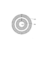
本実施形態では、輪帯照明用の回折光学素子5に代えて、いわゆる周方向偏光輪帯照明用の回折光学素子50を照明光路中に設定することによって、輪帯状の二次光源を通過する光束が周方向偏光状態に設定された変形照明、すなわち周方向偏光輪帯照明を行うことができる。図11は、本実施形態にかかる周方向偏光輪帯照明用の回折光学素子の構成を概略的に示す図である。また、図12は、周方向偏光状態に設定された輪帯状の二次光源を概略的に示す図である。
In this embodiment, instead of the diffractive optical element 5 for annular illumination, a so-called circumferential polarization annular illumination diffractive
図11および図12を参照すると、本実施形態にかかる周方向偏光輪帯照明用の回折光学素子50は、互いに同じ矩形状の断面を有し且つ光の透過方向(Y方向)に沿った厚さ(光軸方向の長さ)が互いに異なる4種類の基本素子50A〜50Dを縦横に且つ稠密に配置することにより構成されている。ここで、第1基本素子50Aの厚さが最も大きく、第4基本素子50Dの厚さが最も小さく、第2基本素子50Bの厚さは第3基本素子50Cの厚さよりも大きく設定されている。
Referring to FIGS. 11 and 12, the diffractive
また、回折光学素子50は、第1基本素子50Aと第2基本素子50Bと第3基本素子50Cと第4基本素子50Dとをほぼ同数含み、4種類の基本素子50A〜50Dはほぼランダム配置されている。さらに、各基本素子50A〜50Dのマスク側には回折面(図中斜線部で示す)が形成され、各基本素子50A〜50Dの回折面が光軸AX(図11では不図示)と直交する1つの平面に沿うように整列されている。その結果、回折光学素子50のマスク側の面は平面状であるが、回折光学素子50の光源側の面は各基本素子50A〜50Dの厚さの違いにより凹凸状になっている。
The diffractive
そして、第1基本素子50Aの回折面は、図12に示す輪帯状の二次光源31のうち、光軸AXを通るZ方向の軸線に関して対称的な一対の円弧状領域31Aを形成するように構成されている。すなわち、図13に示すように、第1基本素子50Aは、回折光学素子50のファーフィールド(ひいては各基本素子50A〜50Dのファーフィールド)50Eに光軸AXを通るZ方向の軸線に関して対称的な一対の円弧状の光強度分布32A(一対の円弧状領域31Aに対応)を形成する機能を有する。
The diffractive surface of the first
第2基本素子50Bの回折面は、光軸AXを通るZ方向の軸線をY軸廻りに−45度回転させた(図12中反時計回りに45度回転させた)軸線に関して対称的な一対の円弧状領域31Bを形成するように構成されている。すなわち、図14に示すように、第2基本素子50Bは、ファーフィールド50Eに、光軸AXを通るZ方向の軸線をY軸廻りに−45度回転させた軸線に関して対称的な一対の円弧状の光強度分布32B(一対の円弧状領域31Bに対応)を形成する機能を有する。
The diffractive surface of the second
第3基本素子50Cの回折面は、光軸AXを通るX方向の軸線に関して対称的な一対の円弧状領域31Cを形成するように構成されている。すなわち、図15に示すように、第3基本素子50Cは、ファーフィールド50Eに、光軸AXを通るX方向の軸線に関して対称的な一対の円弧状の光強度分布32C(一対の円弧状領域31Cに対応)を形成する機能を有する。
The diffractive surface of the third
第4基本素子50Dの回折面は、光軸AXを通るZ方向の軸線をY軸廻りに+45度回転させた(図12中時計回りに45度回転させた)軸線に関して対称的な一対の円弧状領域31Dを形成するように構成されている。すなわち、図16に示すように、第4基本素子50Dは、ファーフィールド50Eに、光軸AXを通るZ方向の軸線をY軸廻りに+45度回転させた軸線に関して対称的な一対の円弧状の光強度分布32D(一対の円弧状領域31Dに対応)を形成する機能を有する。なお、各円弧状領域31A〜31Dの大きさは互いにほぼ等しく、8つの円弧状領域31A〜31Dが互いに重複することなく且つ互いに離間することなく、光軸AXを中心とした輪帯状の二次光源31を構成している。
The diffractive surface of the fourth
また、本実施形態では、各基本素子50A〜50Dが旋光性を有する光学材料である水晶により構成され、各基本素子50A〜50Dの結晶光学軸が光軸AXとほぼ一致するように設定されている。以下、図17を参照して、水晶の旋光性について簡単に説明する。図17を参照すると、厚さdの水晶からなる平行平面板状の光学部材35が、その結晶光学軸と光軸AXとが一致するように配置されている。この場合、光学部材35の旋光性により、入射した直線偏光の偏光方向が光軸AX廻りにθだけ回転した状態で射出される。
In the present embodiment, each of the
このとき、光学部材35の旋光性による偏光方向の回転角θは、光学部材35の厚さdと水晶の旋光能ρとにより、次の式(1)で表わされる。
θ=d・ρ (1)
一般に、水晶の旋光能ρは使用光の波長が短くなると大きくなる傾向があるが、「応用光学II」の第167頁の記述によれば、250.3nmの波長を有する光に対する水晶の旋光能ρは153.9度/mmである。
At this time, the rotation angle θ in the polarization direction due to the optical rotation of the
θ = d · ρ (1)
In general, the optical rotation power ρ of a crystal tends to increase as the wavelength of the light used decreases, but according to the description on page 167 of “Applied Optics II”, the optical rotation power of the crystal with respect to light having a wavelength of 250.3 nm. ρ is 153.9 degrees / mm.
本実施形態において、第1基本素子50Aは、図13に示すように、Z方向に偏光方向を有する直線偏光の光が入射した場合、Z方向をY軸廻りに+180度回転させた方向すなわちZ方向に偏光方向を有する直線偏光の光を射出するように厚さdAが設定されている。その結果、ファーフィールド50Eに形成される一対の円弧状の光強度分布32Aを通過する光束の偏光方向もZ方向になり、図12に示す一対の円弧状領域31Aを通過する光束の偏光方向もZ方向になる。
In the present embodiment, as shown in FIG. 13, in the first
第2基本素子50Bは、図14に示すように、Z方向に偏光方向を有する直線偏光の光が入射した場合、Z方向をY軸廻りに+135度回転させた方向すなわちZ方向をY軸廻りに−45度回転させた方向に偏光方向を有する直線偏光の光を射出するように厚さdBが設定されている。その結果、ファーフィールド50Eに形成される一対の円弧状の光強度分布32Bを通過する光束の偏光方向もZ方向をY軸廻りに−45度回転させた方向になり、図12に示す一対の円弧状領域31Aを通過する光束の偏光方向もZ方向をY軸廻りに−45度回転させた方向になる。
As shown in FIG. 14, in the second
第3基本素子50Cは、図15に示すように、Z方向に偏光方向を有する直線偏光の光が入射した場合、Z方向をY軸廻りに+90度回転させた方向すなわちX方向に偏光方向を有する直線偏光の光を射出するように厚さdCが設定されている。その結果、ファーフィールド50Eに形成される一対の円弧状の光強度分布32Cを通過する光束の偏光方向もX方向になり、図12に示す一対の円弧状領域31Cを通過する光束の偏光方向もX方向になる。
As shown in FIG. 15, when the linearly polarized light having the polarization direction in the Z direction is incident, the third
第4基本素子50Dは、図16に示すように、Z方向に偏光方向を有する直線偏光の光が入射した場合、Z方向をY軸廻りに+45度回転させた方向に偏光方向を有する直線偏光の光を射出するように厚さdDが設定されている。その結果、ファーフィールド50Eに形成される一対の円弧状の光強度分布32Dを通過する光束の偏光方向もZ方向をY軸廻りに+45度回転させた方向になり、図12に示す一対の円弧状領域31Dを通過する光束の偏光方向もZ方向をY軸廻りに+45度回転させた方向になる。
As shown in FIG. 16, in the fourth
本実施形態では、周方向偏光輪帯照明に際して、周方向偏光輪帯照明用の回折光学素子50を照明光路中に設定し、Z方向に偏光方向を有する直線偏光の光を回折光学素子50に入射させる。その結果、マイクロフライアイレンズ12の後側焦点面(すなわち照明瞳またはその近傍)には、図12に示すように、輪帯状の二次光源(輪帯状の照明瞳分布)31が形成され、この輪帯状の二次光源31を通過する光束が周方向偏光状態に設定される。
In the present embodiment, during circumferential polarization annular illumination, a diffractive
周方向偏光状態では、輪帯状の二次光源31を構成する円弧状領域31A〜31Dをそれぞれ通過する光束は、各円弧状領域31A〜31Dの円周方向に沿った中心位置における光軸AXを中心とする円の接線とほぼ一致する偏光方向を有する直線偏光状態になる。
In the circumferential polarization state, the light beams passing through the arc-shaped
このように本実施形態では、入射光束に基づいて所定面に所定の光強度分布を形成するための光束変換素子50が、旋光性を有する光学材料により形成されて、前記入射光束に基づいて前記所定の光強度分布のうちの第1領域分布32Aを形成するための第1基本素子50Aと;旋光性を有する光学材料により形成されて、前記入射光束に基づいて前記所定の光強度分布のうちの第2領域分布32Bを形成するための第2基本素子50Bとを備えており、第1基本素子50Aと第2基本素子50Bとの光の透過方向に沿った厚さが互いに異なっている。
As described above, in the present embodiment, the light
このような構成により、本実施形態では、開口絞りにおいて大きな光量損失が発生する従来技術とは異なり、光束変換素子としての回折光学素子50の回折作用と旋光作用とにより、光量損失を実質的に発生させることなく、周方向偏光状態の輪帯状の二次光源31を形成することができる。
With such a configuration, in the present embodiment, unlike the conventional technique in which a large light amount loss occurs in the aperture stop, the light amount loss is substantially reduced by the diffractive action and the optical rotatory action of the diffractive
ここで、本実施形態の好ましい態様によれば、第1基本素子50Aの厚さおよび第2基本素子50Bの厚さは、直線偏光が入射したときに第1領域分布32Aを形成する直線偏光の偏光方向と第2領域分布32Bを形成する直線偏光の偏光方向とが異なるように設定されている。また、第1領域分布32Aおよび第2領域分布32Bは、所定面における所定点を中心とする所定の輪帯領域である所定輪帯領域の少なくとも一部に位置決めされ、第1領域分布32Aおよび第2領域分布32Bを通過する光束は、所定輪帯領域の円周方向を偏光方向とする直線偏光を主成分とする偏光状態を有することが好ましい。
Here, according to a preferred aspect of the present embodiment, the thickness of the first
この場合、所定の光強度分布は、所定輪帯領域とほぼ同一形状の外形を有し、第1領域分布32Aを通過する光束の偏光状態は、第1領域分布32Aの円周方向に沿った中心位置における所定点を中心とする円の接線方向とほぼ一致した直線偏光成分を有し、第2領域分布32Bを通過する光束の偏光状態は、第2領域分布32Bの円周方向に沿った中心位置における所定点を中心とする円の接線方向とほぼ一致した直線偏光成分を有することが好ましい。あるいは、所定の光強度分布は、所定輪帯領域内に分布する多極状であり、第1領域分布を通過する光束の偏光状態は、第1領域分布の円周方向に沿った中心位置における所定点を中心とする円の接線方向とほぼ一致した直線偏光成分を有し、第2領域分布を通過する光束の偏光状態は、第2領域分布の円周方向に沿った中心位置における所定点を中心とする円の接線方向とほぼ一致した直線偏光成分を有することが好ましい。
In this case, the predetermined light intensity distribution has substantially the same shape as that of the predetermined ring zone region, and the polarization state of the light beam passing through the
また、本実施形態の好ましい態様によれば、第1基本素子および第2基本素子は、使用波長の光に対して100度/mm以上の旋光能を有する光学材料により形成されている。また、第1基本素子および第2基本素子は、水晶により形成されていることが好ましい。また、光束変換素子は、第1基本素子と第2基本素子とをほぼ同数含むことが好ましい。また、第1基本素子および第2基本素子は、回折作用または屈折作用を有することが好ましい。 Further, according to a preferred aspect of the present embodiment, the first basic element and the second basic element are formed of an optical material having an optical rotation power of 100 degrees / mm or more with respect to light of the wavelength used. The first basic element and the second basic element are preferably formed of quartz. Moreover, it is preferable that the light beam conversion element includes substantially the same number of first basic elements and second basic elements. The first basic element and the second basic element preferably have a diffractive action or a refractive action.
また、本実施形態の好ましい態様によれば、第1基本素子は、入射光束に基づいて少なくとも2つの第1領域分布を所定面上に形成し、第2基本素子は、入射光束に基づいて少なくとも2つの第2領域分布を所定面上に形成することが好ましい。また、旋光性を有する光学材料により形成されて、入射光束に基づいて所定の光強度分布のうちの第3領域分布32Cを形成するための第3基本素子50Cと、旋光性を有する光学材料により形成されて、入射光束に基づいて所定の光強度分布のうちの第4領域分布32Dを形成するための第4基本素子50Dとをさらに備えていることが好ましい。
According to a preferred aspect of the present embodiment, the first basic element forms at least two first region distributions on a predetermined plane based on the incident light beam, and the second basic element is at least based on the incident light beam. It is preferable to form two second region distributions on a predetermined surface. Further, the third
また、本実施形態では、入射光束に基づいて、該入射光束の断面形状とは異なる形状の所定の光強度分布を所定面上に形成するための光束変換素子50が、所定面上に所定の光強度分布を形成するための、回折面または屈折面を備え、所定の光強度分布は、所定面における所定点を中心とする所定の輪帯領域である所定輪帯領域の少なくとも一部に分布し、所定輪帯領域を通過する光束変換素子からの光束は、所定輪帯領域の円周方向を偏光方向とする直線偏光を主成分とする偏光状態を有している。
In the present embodiment, the light
このような構成により、本実施形態では、開口絞りにおいて大きな光量損失が発生する従来技術とは異なり、光束変換素子としての回折光学素子50の回折作用と旋光作用とにより、光量損失を実質的に発生させることなく、周方向偏光状態の輪帯状の二次光源31を形成することができる。
With such a configuration, in the present embodiment, unlike the conventional technique in which a large light amount loss occurs in the aperture stop, the light amount loss is substantially reduced by the diffractive action and the optical rotatory action of the diffractive
本実施形態の好ましい態様によれば、所定の光強度分布は、多極形状または輪帯状の外形を有する。また、光束変換素子は、旋光性を有する光学材料により形成されることが好ましい。 According to a preferred aspect of the present embodiment, the predetermined light intensity distribution has a multipolar shape or an annular shape. The light beam conversion element is preferably formed of an optical material having optical activity.
また、本実施形態の照明光学装置は、光源からの光束に基づいて被照射面を照明する照明光学装置であって、照明光学装置の照明瞳またはその近傍に照明瞳分布を形成するために光源からの光束を変換するために上述の光束変換素子を備えている。このような構成により、本実施形態の照明光学装置では、光量損失を良好に抑えつつ、周方向偏光状態の輪帯状の照明瞳分布を形成することができる。 The illumination optical device according to the present embodiment is an illumination optical device that illuminates a surface to be irradiated based on a light beam from a light source, and the light source is used to form an illumination pupil distribution at or near the illumination pupil of the illumination optical device. Is provided with the above-described light beam conversion element. With such a configuration, the illumination optical device of the present embodiment can form a ring-shaped illumination pupil distribution in a circumferentially polarized state while suppressing a light amount loss satisfactorily.
ここで、光束変換素子は、特性の異なる他の光束変換素子と交換可能に構成されていることが好ましい。また、光束変換素子と被照射面との間の光路中に配置された波面分割型のオプティカルインテグレータをさらに備え、光束変換素子は、入射光束に基づいてオプティカルインテグレータの入射面に所定の光強度分布を形成することが好ましい。 Here, the light beam conversion element is preferably configured to be exchangeable with other light beam conversion elements having different characteristics. The optical system further includes a wavefront splitting type optical integrator disposed in the optical path between the light beam conversion element and the irradiated surface, and the light beam conversion element has a predetermined light intensity distribution on the incident surface of the optical integrator based on the incident light beam. Is preferably formed.
また、本実施形態の照明光学装置の好ましい態様によれば、所定面上の光強度分布と、所定輪帯領域を通過する光束変換素子からの光束の偏光状態との少なくとも何れか一方は、光源と被照射面との間の光路中に配置される光学部材による影響を考慮して設定される。また、光束変換素子からの光束の偏光状態を、被照射面に照射される光がS偏光を主成分とする偏光状態となるように設定することが好ましい。 According to a preferred aspect of the illumination optical apparatus of the present embodiment, at least one of the light intensity distribution on the predetermined surface and the polarization state of the light beam from the light beam conversion element passing through the predetermined ring zone region is a light source. Is set in consideration of the influence of the optical member disposed in the optical path between the surface and the irradiated surface. Moreover, it is preferable to set the polarization state of the light beam from the light beam conversion element so that the light irradiated on the irradiated surface is in a polarization state mainly composed of S-polarized light.
また、本実施形態の露光装置は、マスクを照明するための上述の照明光学装置を備え、マスクのパターンを感光性基板上に露光する。ここで、所定面上の光強度分布と、所定輪帯領域を通過する光束変換素子からの光束の偏光状態との少なくとも何れか一方は、光源と感光性基板との間の光路中に配置される光学部材による影響を考慮して設定されることが好ましい。また、光束変換素子からの光束の偏光状態を、感光性基板に照射される光がS偏光を主成分とする偏光状態となるように設定することが好ましい。 Moreover, the exposure apparatus of this embodiment is provided with the above-mentioned illumination optical apparatus for illuminating a mask, and exposes the pattern of a mask on a photosensitive substrate. Here, at least one of the light intensity distribution on the predetermined surface and the polarization state of the light beam from the light beam conversion element passing through the predetermined ring zone region is disposed in the optical path between the light source and the photosensitive substrate. It is preferable to set in consideration of the influence of the optical member. Moreover, it is preferable to set the polarization state of the light beam from the light beam conversion element so that the light irradiated to the photosensitive substrate is in a polarization state mainly composed of S-polarized light.
また、本実施形態の露光方法では、上述の照明光学装置を用いてマスクを照明する照明工程と、マスクのパターンを感光性基板上に露光する露光工程とを含んでいる。ここで、所定面上の光強度分布と、所定輪帯領域を通過する光束変換素子からの光束の偏光状態との少なくとも何れか一方は、光源と感光性基板との間の光路中に配置される光学部材による影響を考慮して設定されることが好ましい。また、光束変換素子からの光束の偏光状態を、感光性基板に照射される光がS偏光を主成分とする偏光状態となるように設定することが好ましい。 Further, the exposure method of the present embodiment includes an illumination process for illuminating the mask using the above-described illumination optical device, and an exposure process for exposing the pattern of the mask onto the photosensitive substrate. Here, at least one of the light intensity distribution on the predetermined surface and the polarization state of the light beam from the light beam conversion element passing through the predetermined ring zone region is disposed in the optical path between the light source and the photosensitive substrate. It is preferable to set in consideration of the influence of the optical member. Moreover, it is preferable to set the polarization state of the light beam from the light beam conversion element so that the light irradiated to the photosensitive substrate is in a polarization state mainly composed of S-polarized light.
換言すれば、本実施形態の照明光学装置では、光量損失を良好に抑えつつ、周方向偏光状態の輪帯状の照明瞳分布を形成することができる。その結果、本実施形態の露光装置では、光量損失を良好に抑えつつ周方向偏光状態の輪帯状の照明瞳分布を形成することのできる照明光学装置を用いているので、適切な照明条件のもとで任意方向の微細パターンを忠実に且つ高スループットで転写することができる。 In other words, in the illumination optical device according to the present embodiment, it is possible to form a ring-shaped illumination pupil distribution in a circumferentially polarized state while suppressing light amount loss satisfactorily. As a result, the exposure apparatus of the present embodiment uses an illumination optical apparatus that can form a ring-shaped illumination pupil distribution in a circumferentially polarized state while suppressing the light amount loss satisfactorily. Thus, a fine pattern in any direction can be transferred faithfully and with high throughput.
なお、周方向偏光状態の輪帯状の照明瞳分布に基づく周方向偏光輪帯照明では、被照射面としてのウェハWに照射される光がS偏光を主成分とする偏光状態になる。ここで、S偏光とは、入射面に対して垂直な方向に偏光方向を持つ直線偏光(入射面に垂直な方向に電気ベクトルが振動している偏光)のことである。ただし、入射面とは、光が媒質の境界面(被照射面:ウェハWの表面)に達したときに、その点での境界面の法線と光の入射方向とを含む面として定義される。 In the circumferential polarization annular illumination based on the annular illumination pupil distribution in the circumferential polarization state, the light irradiated on the wafer W as the irradiated surface is in a polarization state mainly composed of S-polarized light. Here, the S-polarized light is linearly polarized light having a polarization direction in a direction perpendicular to the incident surface (polarized light having an electric vector oscillating in a direction perpendicular to the incident surface). However, the incident surface is defined as a surface including the normal of the boundary surface at that point and the incident direction of light when the light reaches the boundary surface of the medium (surface to be irradiated: the surface of the wafer W). The
なお、上述の実施形態では、互いに同じ矩形状の断面を有する4種類の基本素子50A〜50Dをほぼ同数だけ縦横に且つ稠密にランダム配置することにより、周方向偏光輪帯照明用の回折光学素子50を構成している。しかしながら、これに限定されることなく、各基本素子の数、断面形状、種類数、配置などについて様々な変形例が可能である。
In the above-described embodiment, four types of
また、上述の実施形態では、4種類の基本素子50A〜50Dからなる回折光学素子50を用いて、互いに重複することなく且つ互いに離間することなく配列された8つの円弧状領域31A〜31Dにより、光軸AXを中心とした輪帯状の二次光源31を構成している。しかしながら、これに限定されることなく、輪帯状の二次光源を構成する領域の数、形状、配置などについて様々な変形例が可能である。
Further, in the above-described embodiment, by using the diffractive
具体的には、図18(a)に示すように、たとえば4種類の基本素子からなる回折光学素子を用いて、周方向に沿って互いに離間した8つの円弧状領域からなる周方向偏光状態の8極状の二次光源33aを形成することもできる。また、図18(b)に示すように、たとえば4種類の基本素子からなる回折光学素子を用いて、周方向に沿って互いに離間した4つの円弧状領域からなる周方向偏光状態の4極状の二次光源33bを形成することもできる。なお、これらの8極状の二次光源または4極状の二次光源において、各領域の形状は円弧状に限定されることなく、たとえば円形状や楕円状や扇形状であってもよい。また、図19に示すように、たとえば4種類の基本素子からなる回折光学素子を用いて、周方向に沿って互いに重複した8つの円弧状領域からなる周方向偏光状態の輪帯状の二次光源33cを形成することもできる。
Specifically, as shown in FIG. 18A, for example, by using a diffractive optical element composed of four types of basic elements, a circumferential polarization state composed of eight arc-shaped regions separated from each other along the circumferential direction. An octupole secondary
また、周方向に沿って互いに離間した4つまたは8つの領域からなる周方向偏光状態の4極状または8極状の二次光源の他に、図20(a)に示すように、周方向に沿って互いに離間した6つの領域からなる周方向偏光状態の6極状の二次光源を形成しても良い。また、図20(b)に示すように、周方向に沿って互いに離間した複数の領域からなる周方向偏光状態の多極状の二次光源と、光軸上の領域からなる非偏光状態または直線偏光状態の中心極上の二次光源とを持つ二次光源を形成しても良い。また、周方向に沿って互いに離間した2つの領域からなる周方向偏光状態の2極状の二次光源を形成しても良い。 In addition to a quadrupole or octupole secondary light source having a circumferential polarization state composed of four or eight regions spaced apart from each other along the circumferential direction, as shown in FIG. A hexapolar secondary light source having a circumferential polarization state composed of six regions spaced apart from each other may be formed. In addition, as shown in FIG. 20 (b), a multipolar secondary light source having a circumferential polarization state composed of a plurality of regions spaced apart from each other along the circumferential direction, and a non-polarization state comprising a region on the optical axis or A secondary light source having a secondary light source on the central pole in a linear polarization state may be formed. Moreover, you may form the bipolar secondary light source of the circumferential direction polarization state which consists of two area | regions mutually spaced apart along the circumferential direction.
また、上述の実施形態では、図11に示すように、4種類の基本素子50A〜50Dを個別に形成し、これらの素子を組み合わせることにより回折光学素子50を構成している。しかしながら、これに限定されることなく、1つの水晶基板に対して例えばエッチング加工を施すことにより各基本素子50A〜50Dの射出側の回折面および入射側の凹凸面を形成し、回折光学素子50を一体的に構成することもできる。
In the above-described embodiment, as shown in FIG. 11, four types of
また、上述の実施形態では、水晶を用いて各基本素子50A〜50Dを(ひいては回折光学素子50を)形成している。しかしながら、これに限定されることなく、旋光性を有する他の適当な光学材料を用いて各基本素子を形成することもできる。この場合、使用波長の光に対して100度/mm以上の旋光能を有する光学材料を用いることが好ましい。すなわち、旋光能の小さい光学材料を用いると、偏光方向の所要回転角を得るために必要な厚さが大きくなり過ぎて、光量損失の原因になるので好ましくない。
In the above-described embodiment, the
また、上述の実施形態では、輪帯状の照明瞳分布(二次光源)を形成しているが、これに限定されることなく、照明瞳またはその近傍に円形状の照明瞳分布を形成することもできる。また、輪帯形状の照明瞳分布や多極形状の照明瞳分布に加えて、たとえば光軸を含む中心領域分布を形成することにより、いわゆる中心極を伴う輪帯照明や中心極を伴う複数極照明を行うこともできる。 In the above embodiment, the annular illumination pupil distribution (secondary light source) is formed. However, the present invention is not limited to this, and a circular illumination pupil distribution is formed in or near the illumination pupil. You can also. Moreover, in addition to the annular illumination pupil distribution and the multipolar illumination pupil distribution, for example, by forming a central region distribution including the optical axis, annular illumination with a so-called central pole or multiple poles with a central pole Lighting can also be performed.
また、上述の実施形態では、照明瞳またはその近傍において周方向偏光状態の照明瞳分布を形成している。しかしながら、光束変換素子としての回折光学素子よりもウェハ側の光学系(照明光学系や投影光学系)の偏光収差(リターデーション)に起因して偏光方向が変わることがある。この場合には、これらの光学系の偏光収差の影響を考慮した上で、照明瞳またはその近傍に形成される照明瞳分布を通過する光束の偏光状態を適宜設定する必要がある。 In the above-described embodiment, the illumination pupil distribution in the circumferential polarization state is formed at or near the illumination pupil. However, the polarization direction may change due to polarization aberration (retardation) of the optical system (illumination optical system or projection optical system) on the wafer side of the diffractive optical element as the light beam conversion element. In this case, it is necessary to appropriately set the polarization state of the light beam passing through the illumination pupil distribution formed in or near the illumination pupil in consideration of the influence of the polarization aberration of these optical systems.
また、上記の偏光収差に関連して、光束変換素子よりもウェハ側の光学系(照明光学系や投影光学系)中に配置された反射部材の偏光特性に起因して、反射光が偏光方向ごとに位相差を有することがある。この場合においても、反射部材の偏光特性に起因する位相差の影響を考慮した上で、照明瞳またはその近傍に形成される照明瞳分布を通過する光束の偏光状態を適宜設定する必要がある。 Further, in relation to the above-described polarization aberration, the reflected light is polarized in the polarization direction due to the polarization characteristics of the reflecting member disposed in the optical system (illumination optical system or projection optical system) on the wafer side of the light beam conversion element. Each may have a phase difference. Even in this case, it is necessary to appropriately set the polarization state of the light beam passing through the illumination pupil distribution or the illumination pupil distribution formed in the vicinity thereof in consideration of the influence of the phase difference caused by the polarization characteristics of the reflecting member.
また、光束変換素子よりもウェハ側の光学系(照明光学系や投影光学系)中に配置された反射部材の偏光特性に起因して、反射部材における反射率が偏光方向により変化することがある。この場合、偏光方向ごとの反射率を考慮して、照明瞳またはその近傍に形成される光強度分布にオフセットをのせること、すなわち各基本素子の数に分布を設けることが好ましい。また、光束変換素子よりもウェハ側の光学系における透過率が偏光方向により変化する場合にも、上記手法を同様に適用することができる。 Further, due to the polarization characteristics of the reflecting member disposed in the optical system (illumination optical system or projection optical system) on the wafer side with respect to the light beam conversion element, the reflectance of the reflecting member may vary depending on the polarization direction. . In this case, in consideration of the reflectance for each polarization direction, it is preferable to offset the light intensity distribution formed at or near the illumination pupil, that is, to provide a distribution in the number of each basic element. In addition, the above method can be similarly applied when the transmittance in the optical system on the wafer side with respect to the light beam conversion element varies depending on the polarization direction.
また、上述の実施形態では、回折光学素子50の光源側の面は各基本素子50A〜50Dの厚さの違いにより段差を有する凹凸状になっている。そこで、図21に示すように、厚さの最も大きい第1基本素子50A以外の基本素子、すなわち第2基本素子50B、第3基本素子50Cおよび第4基本素子50Dの入射側に補正部材36を付設して、回折光学素子50の光源側(入射側)の面も平面状に構成することができる。この場合、旋光性を有しない光学材料を用いて補正部材36を形成することになる。
In the above-described embodiment, the surface on the light source side of the diffractive
また、上述の実施形態では、照明瞳またはその近傍に形成される照明瞳分布を通過する光束が円周方向に沿った直線偏光成分のみを有する例を示している。しかしながら、これに限定されることなく、照明瞳分布を通過する光束の偏光状態が円周方向を偏光方向とする直線偏光を主成分とする状態であれば、本発明の所要の効果を得ることができる。 In the above-described embodiment, an example is shown in which a light beam passing through an illumination pupil distribution formed in or near the illumination pupil has only a linearly polarized component along the circumferential direction. However, the present invention is not limited to this, and the required effect of the present invention can be obtained if the polarization state of the light beam passing through the illumination pupil distribution is a state in which the main component is linearly polarized light whose polarization direction is the circumferential direction. Can do.
また、上述の実施形態では、入射光束に基づいて、その断面形状とは異なる形状の光強度分布を所定面上に形成するための光束変換素子として、回折作用を有する複数種類の基本素子からなる回折光学素子を用いている。しかしながら、これに限定されることなく、たとえば各基本素子の回折面と光学的にほぼ等価な屈折面を有する複数種類の基本素子、すなわち屈折作用を有する複数種類の基本素子からなる屈折光学素子を光束変換素子として用いていることもできる。 In the above-described embodiment, the light beam conversion element for forming the light intensity distribution having a shape different from the cross-sectional shape on the predetermined surface based on the incident light beam is composed of a plurality of types of basic elements having a diffractive action. A diffractive optical element is used. However, the present invention is not limited to this. For example, a plurality of types of basic elements having refractive surfaces that are optically substantially equivalent to the diffractive surfaces of the basic elements, that is, refractive optical elements composed of a plurality of types of basic elements having a refractive action are provided. It can also be used as a light beam conversion element.
上述の実施形態にかかる露光装置では、照明光学装置によってマスク(レチクル)を照明し(照明工程)、投影光学系を用いてマスクに形成された転写用のパターンを感光性基板に露光する(露光工程)ことにより、マイクロデバイス(半導体素子、撮像素子、液晶表示素子、薄膜磁気ヘッド等)を製造することができる。以下、上述の実施形態の露光装置を用いて感光性基板としてのウェハ等に所定の回路パターンを形成することによって、マイクロデバイスとしての半導体デバイスを得る際の手法の一例につき図22のフローチャートを参照して説明する。 In the exposure apparatus according to the above-described embodiment, the illumination optical device illuminates the mask (reticle) (illumination process), and the projection optical system is used to expose the transfer pattern formed on the mask onto the photosensitive substrate (exposure). Step), a micro device (semiconductor element, imaging element, liquid crystal display element, thin film magnetic head, etc.) can be manufactured. Refer to the flowchart of FIG. 22 for an example of a method for obtaining a semiconductor device as a micro device by forming a predetermined circuit pattern on a wafer or the like as a photosensitive substrate using the exposure apparatus of the above-described embodiment. To explain.
先ず、図22のステップ301において、1ロットのウェハ上に金属膜が蒸着される。次のステップ302において、その1ロットのウェハ上の金属膜上にフォトレジストが塗布される。その後、ステップ303において、上述の実施形態の露光装置を用いて、マスク上のパターンの像がその投影光学系を介して、その1ロットのウェハ上の各ショット領域に順次露光転写される。その後、ステップ304において、その1ロットのウェハ上のフォトレジストの現像が行われた後、ステップ305において、その1ロットのウェハ上でレジストパターンをマスクとしてエッチングを行うことによって、マスク上のパターンに対応する回路パターンが、各ウェハ上の各ショット領域に形成される。その後、更に上のレイヤの回路パターンの形成等を行うことによって、半導体素子等のデバイスが製造される。上述の半導体デバイス製造方法によれば、極めて微細な回路パターンを有する半導体デバイスをスループット良く得ることができる。 First, in step 301 of FIG. 22, a metal film is deposited on one lot of wafers. In the next step 302, a photoresist is applied on the metal film on the one lot of wafers. Thereafter, in step 303, the image of the pattern on the mask is sequentially exposed and transferred to each shot area on the wafer of one lot through the projection optical system using the exposure apparatus of the above-described embodiment. Thereafter, in step 304, the photoresist on the one lot of wafers is developed, and in step 305, the resist pattern is etched on the one lot of wafers to form a pattern on the mask. Corresponding circuit patterns are formed in each shot area on each wafer. Thereafter, a device pattern such as a semiconductor element is manufactured by forming a circuit pattern of an upper layer. According to the semiconductor device manufacturing method described above, a semiconductor device having an extremely fine circuit pattern can be obtained with high throughput.
また、上述の実施形態の露光装置では、プレート(ガラス基板)上に所定のパターン(回路パターン、電極パターン等)を形成することによって、マイクロデバイスとしての液晶表示素子を得ることもできる。以下、図23のフローチャートを参照して、このときの手法の一例につき説明する。図23において、パターン形成工程401では、上述の実施形態の露光装置を用いてマスクのパターンを感光性基板(レジストが塗布されたガラス基板等)に転写露光する、所謂光リソグラフィー工程が実行される。この光リソグラフィー工程によって、感光性基板上には多数の電極等を含む所定パターンが形成される。その後、露光された基板は、現像工程、エッチング工程、レジスト剥離工程等の各工程を経ることによって、基板上に所定のパターンが形成され、次のカラーフィルター形成工程402へ移行する。 In the exposure apparatus of the above-described embodiment, a liquid crystal display element as a micro device can be obtained by forming a predetermined pattern (circuit pattern, electrode pattern, etc.) on a plate (glass substrate). Hereinafter, an example of the technique at this time will be described with reference to the flowchart of FIG. In FIG. 23, in the pattern forming process 401, a so-called photolithography process is performed in which the exposure pattern of the above-described embodiment is used to transfer and expose a mask pattern onto a photosensitive substrate (such as a glass substrate coated with a resist). . By this photolithography process, a predetermined pattern including a large number of electrodes and the like is formed on the photosensitive substrate. Thereafter, the exposed substrate undergoes steps such as a developing step, an etching step, and a resist stripping step, whereby a predetermined pattern is formed on the substrate, and the process proceeds to the next color filter forming step 402.
次に、カラーフィルター形成工程402では、R(Red)、G(Green)、B(Blue)に対応した3つのドットの組がマトリックス状に多数配列されたり、またはR、G、Bの3本のストライプのフィルターの組を複数水平走査線方向に配列したカラーフィルターを形成する。そして、カラーフィルター形成工程402の後に、セル組み立て工程403が実行される。セル組み立て工程403では、パターン形成工程401にて得られた所定パターンを有する基板、およびカラーフィルター形成工程402にて得られたカラーフィルター等を用いて液晶パネル(液晶セル)を組み立てる。 Next, in the color filter forming step 402, a large number of sets of three dots corresponding to R (Red), G (Green), and B (Blue) are arranged in a matrix or three of R, G, and B A color filter is formed by arranging a plurality of stripe filter sets in the horizontal scanning line direction. Then, after the color filter forming step 402, a cell assembly step 403 is executed. In the cell assembly step 403, a liquid crystal panel (liquid crystal cell) is assembled using the substrate having the predetermined pattern obtained in the pattern formation step 401, the color filter obtained in the color filter formation step 402, and the like.
セル組み立て工程403では、例えば、パターン形成工程401にて得られた所定パターンを有する基板とカラーフィルター形成工程402にて得られたカラーフィルターとの間に液晶を注入して、液晶パネル(液晶セル)を製造する。その後、モジュール組み立て工程404にて、組み立てられた液晶パネル(液晶セル)の表示動作を行わせる電気回路、バックライト等の各部品を取り付けて液晶表示素子として完成させる。上述の液晶表示素子の製造方法によれば、極めて微細な回路パターンを有する液晶表示素子をスループット良く得ることができる。 In the cell assembly step 403, for example, liquid crystal is injected between the substrate having the predetermined pattern obtained in the pattern formation step 401 and the color filter obtained in the color filter formation step 402, and a liquid crystal panel (liquid crystal cell) is obtained. ). Thereafter, in a module assembling step 404, components such as an electric circuit and a backlight for performing a display operation of the assembled liquid crystal panel (liquid crystal cell) are attached to complete a liquid crystal display element. According to the above-described method for manufacturing a liquid crystal display element, a liquid crystal display element having an extremely fine circuit pattern can be obtained with high throughput.
なお、上述の実施形態では、露光光としてKrFエキシマレーザ光(波長:248nm)やArFエキシマレーザ光(波長:193nm)を用いているが、これに限定されることなく、他の適当なレーザ光源、たとえば波長157nmのレーザ光を供給するF2レーザ光源などに対して本発明を適用することもできる。さらに、上述の実施形態では、照明光学装置を備えた露光装置を例にとって本発明を説明したが、マスクやウェハ以外の被照射面を照明するための一般的な照明光学装置に本発明を適用することができることは明らかである。 In the above-described embodiment, KrF excimer laser light (wavelength: 248 nm) or ArF excimer laser light (wavelength: 193 nm) is used as the exposure light. However, the present invention is not limited to this, and other suitable laser light sources. For example, the present invention can also be applied to an F 2 laser light source that supplies laser light having a wavelength of 157 nm. Furthermore, in the above-described embodiment, the present invention has been described by taking an exposure apparatus provided with an illumination optical apparatus as an example. Obviously you can do that.
また、上述の実施形態において、投影光学系と感光性基板との間の光路中を1.1よりも大きな屈折率を有する媒体(典型的には液体)で満たす手法、所謂液浸法を適用しても良い。この場合、投影光学系と感光性基板との間の光路中に液体を満たす手法としては、国際公開番号WO99/49504号公報に開示されているような局所的に液体を満たす手法や、特開平6−124873号公報に開示されているような露光対象の基板を保持したステージを液槽の中で移動させる手法や、特開平10−303114号公報に開示されているようなステージ上に所定深さの液体槽を形成し、その中に基板を保持する手法などを採用することができる。ここでは、国際公開番号WO99/49504号公報、特開平6−124873号公報および特開平10−303114号公報を参照として援用する。 In the above-described embodiment, a so-called immersion method is applied in which the optical path between the projection optical system and the photosensitive substrate is filled with a medium (typically liquid) having a refractive index larger than 1.1. You may do it. In this case, as a method of filling the liquid in the optical path between the projection optical system and the photosensitive substrate, a method of locally filling the liquid as disclosed in International Publication No. WO99 / 49504, A method of moving a stage holding a substrate to be exposed as disclosed in Japanese Patent Application Laid-Open No. 6-124873 in a liquid bath, or a predetermined depth on a stage as disclosed in Japanese Patent Application Laid-Open No. 10-303114. A technique of forming a liquid tank and holding the substrate in the liquid tank can be employed. Here, International Publication Nos. WO99 / 49504, JP-A-6-124873, and JP-A-10-303114 are incorporated by reference.
なお、液体としては、露光光に対する透過性があってできるだけ屈折率が高く、投影光学系や基板表面に塗布されているフォトレジストに対して安定なものを用いることが好ましく、たとえばKrFエキシマレーザ光やArFエキシマレーザ光を露光光とする場合には、液体として純水、脱イオン水を用いることができる。また、露光光としてF2レーザ光を用いる場合は、液体としてはF2レーザ光を透過可能な例えばフッ素系オイルや過フッ化ポリエーテル(PFPE)等のフッ素系の液体を用いればよい。 As the liquid, it is preferable to use a liquid that is transmissive to exposure light and has a refractive index as high as possible, and is stable with respect to a photoresist applied to the projection optical system and the substrate surface, for example, KrF excimer laser light. When ArF excimer laser light is used as exposure light, pure water or deionized water can be used as the liquid. When F 2 laser light is used as exposure light, a fluorine-based liquid such as fluorine oil or perfluorinated polyether (PFPE) that can transmit the F 2 laser light may be used as the liquid.
1 光源
4 偏光状態切換手段
4a 1/4波長板
4b 1/2波長板
4c デポラライザ
5,50 回折光学素子(光束変換素子)
6 アフォーカルレンズ
8 円錐アキシコン系
9,10 シリンドリカルレンズ対
11 ズームレンズ
12 マイクロフライアイレンズ
13 偏光モニター
13a ビームスプリッター
14 コンデンサー光学系
15 マスクブラインド
16 結像光学系
M マスク
PL 投影光学系
W ウェハ
DESCRIPTION OF SYMBOLS 1 Light source 4 Polarization state switching means 4a 1/4
6
Claims (28)
入射する光の偏光状態を切り換えて射出する偏光状態切換手段と、
前記偏光状態切換手段と前記被照射面との間の光路に配置された光束変換素子と、
前記光束変換素子と、前記照明光学装置の照明瞳面またはその近傍の面である所定面との間に配置された部分光学系とを備え、
前記光束変換素子は、旋光性を有する光学材料により形成されて、入射する直線偏光状態の光束に基づいて、前記部分光学系と協働して前記所定面上の第1領域分布に第1偏光状態の第1光強度分布を形成するための第1基本素子と、旋光性を有する光学材料により形成されて、前記入射する直線偏光状態の光束に基づいて、前記部分光学系と協働して前記所定面上の第2領域分布に第2偏光状態の第2光強度分布を形成するための第2基本素子とを備え、
前記第1基本素子と前記第2基本素子とは、前記照明光学装置の光軸方向に沿った厚さが互いに異なることを特徴とする照明光学装置。
In the illumination optical device that illuminates the illuminated surface based on the light flux from the light source,
Polarization state switching means for switching and emitting the polarization state of incident light; and
A light beam conversion element disposed in an optical path between the polarization state switching means and the irradiated surface;
Comprising said light beam conversion element, and a portion disposed optical system between the predetermined surface is the illumination pupil plane or plane in the vicinity of the front Symbol illumination optical apparatus,
The light beam conversion element is formed of an optical material having optical rotation, and is based on an incident linearly polarized light beam and cooperates with the partial optical system to form a first polarized light in a first region distribution on the predetermined surface. The first basic element for forming the first light intensity distribution of the state and an optical material having optical rotation, and based on the incident linearly polarized light beam , in cooperation with the partial optical system A second basic element for forming a second light intensity distribution of a second polarization state in a second region distribution on the predetermined plane,
The illumination optical apparatus according to claim 1, wherein the first basic element and the second basic element have different thicknesses along the optical axis direction of the illumination optical apparatus .
前記第1領域分布および前記第2領域分布を通過する光束は、前記所定輪帯領域の円周方向を偏光方向とする直線偏光を主成分とする偏光状態を有することを特徴とする請求項1または2に記載の照明光学装置。 The first region distribution and the second region distribution are positioned on at least a part of a predetermined annular region that is a predetermined annular region centered on a predetermined point on the predetermined surface ,
The light beam passing through the first region distribution and the second region distribution has a polarization state in which linearly polarized light whose polarization direction is a circumferential direction of the predetermined annular region is a main component. Or the illumination optical apparatus of 2.
前記第1領域分布を通過する光束の第1偏光状態は、前記第1領域分布の円周方向に沿った中心位置における前記所定点を中心とする円の接線方向とほぼ一致した直線偏光成分を有し、
前記第2領域分布を通過する光束の第2偏光状態は、前記第2領域分布の円周方向に沿った中心位置における前記所定点を中心とする円の接線方向とほぼ一致した直線偏光成分を有することを特徴とする請求項3に記載の照明光学装置。 The light intensity distribution having the predetermined polarization characteristic has an outer shape that is substantially the same shape as the predetermined annular zone region,
The first polarization state of the light beam passing through the first region distribution is a linearly polarized light component that substantially coincides with the tangential direction of the circle centered on the predetermined point at the center position along the circumferential direction of the first region distribution. Have
The second polarization state of the light beam passing through the second region distribution is a linearly polarized light component that substantially coincides with the tangential direction of the circle centered on the predetermined point at the center position along the circumferential direction of the second region distribution. The illumination optical apparatus according to claim 3, wherein the illumination optical apparatus is provided.
前記第1領域分布を通過する光束の第1偏光状態は、前記第1領域分布の円周方向に沿った中心位置における前記所定点を中心とする円の接線方向とほぼ一致した直線偏光成分を有し、
前記第2領域分布を通過する光束の第2偏光状態は、前記第2領域分布の円周方向に沿った中心位置における前記所定点を中心とする円の接線方向とほぼ一致した直線偏光成分を有することを特徴とする請求項3に記載の照明光学装置。 The light intensity distribution having the predetermined polarization characteristic is multipolar distributed in the predetermined annular zone region,
The first polarization state of the light beam passing through the first region distribution is a linearly polarized light component that substantially coincides with the tangential direction of the circle centered on the predetermined point at the center position along the circumferential direction of the first region distribution. Have
The second polarization state of the light beam passing through the second region distribution is a linearly polarized light component that substantially coincides with the tangential direction of the circle centered on the predetermined point at the center position along the circumferential direction of the second region distribution. The illumination optical apparatus according to claim 3, wherein the illumination optical apparatus is provided.
旋光性を有する光学材料により形成されて、前記入射する直線偏光状態の光束に基づいて前記所定の偏光特性を持つ光強度分布のうち第4領域分布にて第4偏光状態の第4光強度分布を形成するための第4基本素子とをさらに備えることを特徴とする請求項1乃至9のいずれか1項に記載の照明光学装置。
The light beam conversion element is formed of an optical material having optical rotation, and a third polarization state in a third region distribution among light intensity distributions having the predetermined polarization characteristics based on the incident linearly polarized light beam. A third basic element for forming a third light intensity distribution of
A fourth light intensity distribution in a fourth polarization state in a fourth region distribution among light intensity distributions formed of an optical material having optical rotation and having the predetermined polarization characteristics based on the incident linearly polarized light flux The illumination optical apparatus according to claim 1, further comprising: a fourth basic element for forming the first and second elements.
前記第3領域分布および前記第4領域分布を通過する光束は、前記所定輪帯領域の円周方向を偏光方向とする直線偏光を主成分とする偏光状態を有することを特徴とする請求項10または11に記載の照明光学装置。 The third region distribution and the fourth region distribution are positioned on at least a part of a predetermined annular region that is a predetermined annular region centered on a predetermined point on the illumination pupil of the illumination optical device or a surface in the vicinity thereof. ,
11. The light flux passing through the third region distribution and the fourth region distribution has a polarization state mainly composed of linearly polarized light whose polarization direction is a circumferential direction of the predetermined annular region. Or the illumination optical apparatus of 11.
前記第3領域分布を通過する光束の第3偏光状態は、前記第3領域分布の円周方向に沿った中心位置における前記所定点を中心とする円の接線方向とほぼ一致した直線偏光成分を有し、
前記第4領域分布を通過する光束の第4偏光状態は、前記第4領域分布の円周方向に沿った中心位置における前記所定点を中心とする円の接線方向とほぼ一致した直線偏光成分を有することを特徴とする請求項12に記載の照明光学装置。 The light intensity distribution having the predetermined polarization characteristic has an outer shape that is substantially the same shape as the predetermined annular zone region,
The third polarization state of the light beam passing through the third region distribution has a linearly polarized light component substantially coincident with a tangential direction of a circle centered on the predetermined point at the center position along the circumferential direction of the third region distribution. Have
The fourth polarization state of the light beam passing through the fourth region distribution has a linearly polarized light component substantially coincident with a tangential direction of a circle centered on the predetermined point at the center position along the circumferential direction of the fourth region distribution. The illumination optical apparatus according to claim 12, comprising:
前記第3領域分布を通過する光束の第3偏光状態は、前記第3領域分布の円周方向に沿った中心位置における前記所定点を中心とする円の接線方向とほぼ一致した直線偏光成分を有し、
前記第4領域分布を通過する光束の第4偏光状態は、前記第4領域分布の円周方向に沿った中心位置における前記所定点を中心とする円の接線方向とほぼ一致した直線偏光成分を有することを特徴とする請求項12に記載の照明光学装置。 The light intensity distribution having the predetermined polarization characteristic is multipolar distributed in the predetermined annular zone region,
The third polarization state of the light beam passing through the third region distribution has a linearly polarized light component substantially coincident with a tangential direction of a circle centered on the predetermined point at the center position along the circumferential direction of the third region distribution. Have
The fourth polarization state of the light beam passing through the fourth region distribution has a linearly polarized light component substantially coincident with a tangential direction of a circle centered on the predetermined point at the center position along the circumferential direction of the fourth region distribution. The illumination optical apparatus according to claim 12, comprising:
前記光束変換素子は、入射光束に基づいて前記オプティカルインテグレータの入射面に所定の光強度分布を形成することを特徴とする請求項1乃至20のいずれか1項に記載の照明光学装置。 A wavefront splitting type optical integrator disposed in an optical path between the light flux conversion element and the irradiated surface;
21. The illumination optical apparatus according to claim 1, wherein the light beam conversion element forms a predetermined light intensity distribution on an incident surface of the optical integrator based on an incident light beam .
Priority Applications (1)
| Application Number | Priority Date | Filing Date | Title |
|---|---|---|---|
| JP2006262589A JP4976094B2 (en) | 2003-11-20 | 2006-09-27 | Illumination optical apparatus, exposure apparatus, exposure method, and microdevice manufacturing method |
Applications Claiming Priority (3)
| Application Number | Priority Date | Filing Date | Title |
|---|---|---|---|
| JP2003390674 | 2003-11-20 | ||
| JP2003390674 | 2003-11-20 | ||
| JP2006262589A JP4976094B2 (en) | 2003-11-20 | 2006-09-27 | Illumination optical apparatus, exposure apparatus, exposure method, and microdevice manufacturing method |
Related Parent Applications (1)
| Application Number | Title | Priority Date | Filing Date |
|---|---|---|---|
| JP2005515570A Division JP4976015B2 (en) | 2003-11-20 | 2004-11-02 | Flux conversion element, illumination optical device, exposure apparatus, and exposure method |
Publications (2)
| Publication Number | Publication Date |
|---|---|
| JP2006345006A JP2006345006A (en) | 2006-12-21 |
| JP4976094B2 true JP4976094B2 (en) | 2012-07-18 |
Family
ID=37641660
Family Applications (1)
| Application Number | Title | Priority Date | Filing Date |
|---|---|---|---|
| JP2006262589A Active JP4976094B2 (en) | 2003-11-20 | 2006-09-27 | Illumination optical apparatus, exposure apparatus, exposure method, and microdevice manufacturing method |
Country Status (1)
| Country | Link |
|---|---|
| JP (1) | JP4976094B2 (en) |
Cited By (4)
| Publication number | Priority date | Publication date | Assignee | Title |
|---|---|---|---|---|
| US20130271945A1 (en) | 2004-02-06 | 2013-10-17 | Nikon Corporation | Polarization-modulating element, illumination optical apparatus, exposure apparatus, and exposure method |
| JP2014003306A (en) * | 2003-11-20 | 2014-01-09 | Nikon Corp | Light flux conversion element, illumination optical device, exposure device, and exposure method |
| US9423698B2 (en) | 2003-10-28 | 2016-08-23 | Nikon Corporation | Illumination optical apparatus and projection exposure apparatus |
| US9678437B2 (en) | 2003-04-09 | 2017-06-13 | Nikon Corporation | Illumination optical apparatus having distribution changing member to change light amount and polarization member to set polarization in circumference direction |
Families Citing this family (3)
| Publication number | Priority date | Publication date | Assignee | Title |
|---|---|---|---|---|
| JP4971932B2 (en) | 2007-10-01 | 2012-07-11 | キヤノン株式会社 | Illumination optical system, exposure apparatus, device manufacturing method, and polarization control unit |
| JP2012073413A (en) * | 2010-09-29 | 2012-04-12 | Kyocera Kinseki Corp | Polarization conversion element and method for manufacturing polarization conversion element |
| JP2012073414A (en) * | 2010-09-29 | 2012-04-12 | Kyocera Kinseki Corp | Polarization conversion element and method for manufacturing polarization conversion element |
Family Cites Families (11)
| Publication number | Priority date | Publication date | Assignee | Title |
|---|---|---|---|---|
| JP3246615B2 (en) * | 1992-07-27 | 2002-01-15 | 株式会社ニコン | Illumination optical device, exposure apparatus, and exposure method |
| JPH06188169A (en) * | 1992-08-24 | 1994-07-08 | Canon Inc | Method of image formation, exposure system, and manufacture of device |
| JPH06124872A (en) * | 1992-10-14 | 1994-05-06 | Canon Inc | Image forming method and manufacture of semiconductor device using the method |
| JPH07183201A (en) * | 1993-12-21 | 1995-07-21 | Nec Corp | Exposure device and method therefor |
| JPH07263315A (en) * | 1994-03-25 | 1995-10-13 | Toshiba Corp | Projection aligner |
| JPH07283119A (en) * | 1994-04-14 | 1995-10-27 | Hitachi Ltd | Aligner and exposure method |
| DE19535392A1 (en) * | 1995-09-23 | 1997-03-27 | Zeiss Carl Fa | Radial polarization-rotating optical arrangement and microlithography projection exposure system with it |
| JP3406957B2 (en) * | 1995-12-06 | 2003-05-19 | キヤノン株式会社 | Optical element and exposure apparatus using the same |
| JP2001272764A (en) * | 2000-03-24 | 2001-10-05 | Canon Inc | Photomask for projection exposure and for projection exposure method using the photomask |
| DE10124803A1 (en) * | 2001-05-22 | 2002-11-28 | Zeiss Carl | Polarizer and microlithography projection system with polarizer |
| JP2003297727A (en) * | 2002-04-03 | 2003-10-17 | Nikon Corp | Illumination optical device, exposure apparatus, and method of exposure |
-
2006
- 2006-09-27 JP JP2006262589A patent/JP4976094B2/en active Active
Cited By (14)
| Publication number | Priority date | Publication date | Assignee | Title |
|---|---|---|---|---|
| US9885959B2 (en) | 2003-04-09 | 2018-02-06 | Nikon Corporation | Illumination optical apparatus having deflecting member, lens, polarization member to set polarization in circumference direction, and optical integrator |
| US9678437B2 (en) | 2003-04-09 | 2017-06-13 | Nikon Corporation | Illumination optical apparatus having distribution changing member to change light amount and polarization member to set polarization in circumference direction |
| US9423698B2 (en) | 2003-10-28 | 2016-08-23 | Nikon Corporation | Illumination optical apparatus and projection exposure apparatus |
| US9760014B2 (en) | 2003-10-28 | 2017-09-12 | Nikon Corporation | Illumination optical apparatus and projection exposure apparatus |
| JP2015008304A (en) * | 2003-11-20 | 2015-01-15 | 株式会社ニコン | Light flux conversion element, illumination optical device, exposure device, and exposure method |
| JP2016026306A (en) * | 2003-11-20 | 2016-02-12 | 株式会社ニコン | Light flux conversion device, illumination optical device, exposure device and exposure method |
| JP2016212434A (en) * | 2003-11-20 | 2016-12-15 | 株式会社ニコン | Light flux conversion element, illumination optical device, exposure apparatus, and exposure method |
| JP2014003305A (en) * | 2003-11-20 | 2014-01-09 | Nikon Corp | Illumination optical device, exposure device, exposure method, and device manufacturing method |
| JP2014003306A (en) * | 2003-11-20 | 2014-01-09 | Nikon Corp | Light flux conversion element, illumination optical device, exposure device, and exposure method |
| US10281632B2 (en) | 2003-11-20 | 2019-05-07 | Nikon Corporation | Illumination optical apparatus, exposure apparatus, and exposure method with optical member with optical rotatory power to rotate linear polarization direction |
| US20130271945A1 (en) | 2004-02-06 | 2013-10-17 | Nikon Corporation | Polarization-modulating element, illumination optical apparatus, exposure apparatus, and exposure method |
| US10007194B2 (en) | 2004-02-06 | 2018-06-26 | Nikon Corporation | Polarization-modulating element, illumination optical apparatus, exposure apparatus, and exposure method |
| US10234770B2 (en) | 2004-02-06 | 2019-03-19 | Nikon Corporation | Polarization-modulating element, illumination optical apparatus, exposure apparatus, and exposure method |
| US10241417B2 (en) | 2004-02-06 | 2019-03-26 | Nikon Corporation | Polarization-modulating element, illumination optical apparatus, exposure apparatus, and exposure method |
Also Published As
| Publication number | Publication date |
|---|---|
| JP2006345006A (en) | 2006-12-21 |
Similar Documents
| Publication | Publication Date | Title |
|---|---|---|
| JP6493325B2 (en) | Flux conversion element, illumination optical device, exposure apparatus, and exposure method | |
| JP6399133B2 (en) | Polarization conversion element, illumination optical apparatus, exposure apparatus, and exposure method | |
| JP2006196715A (en) | Luminous-flux converting element, illuminating optical apparatus, exposure apparatus, and exposure method | |
| JPWO2006016469A1 (en) | Illumination optical apparatus, exposure apparatus, and exposure method | |
| JP4976094B2 (en) | Illumination optical apparatus, exposure apparatus, exposure method, and microdevice manufacturing method | |
| JP4748015B2 (en) | Illumination optical apparatus, exposure apparatus, exposure method, and microdevice manufacturing method | |
| JP4752702B2 (en) | Illumination optical apparatus, exposure apparatus, and device manufacturing method | |
| JP2006100429A (en) | Projection optical system, exposure device, and exposure method |
Legal Events
| Date | Code | Title | Description |
|---|---|---|---|
| A621 | Written request for application examination |
Free format text: JAPANESE INTERMEDIATE CODE: A621 Effective date: 20070828 |
|
| A131 | Notification of reasons for refusal |
Free format text: JAPANESE INTERMEDIATE CODE: A131 Effective date: 20100225 |
|
| A521 | Written amendment |
Free format text: JAPANESE INTERMEDIATE CODE: A523 Effective date: 20100402 |
|
| RD03 | Notification of appointment of power of attorney |
Free format text: JAPANESE INTERMEDIATE CODE: A7423 Effective date: 20100621 |
|
| RD04 | Notification of resignation of power of attorney |
Free format text: JAPANESE INTERMEDIATE CODE: A7424 Effective date: 20100621 |
|
| A02 | Decision of refusal |
Free format text: JAPANESE INTERMEDIATE CODE: A02 Effective date: 20100803 |
|
| A521 | Written amendment |
Free format text: JAPANESE INTERMEDIATE CODE: A523 Effective date: 20111219 |
|
| A521 | Written amendment |
Free format text: JAPANESE INTERMEDIATE CODE: A523 Effective date: 20120316 |
|
| A01 | Written decision to grant a patent or to grant a registration (utility model) |
Free format text: JAPANESE INTERMEDIATE CODE: A01 |
|
| A61 | First payment of annual fees (during grant procedure) |
Free format text: JAPANESE INTERMEDIATE CODE: A61 Effective date: 20120412 |
|
| R150 | Certificate of patent or registration of utility model |
Ref document number: 4976094 Country of ref document: JP Free format text: JAPANESE INTERMEDIATE CODE: R150 Free format text: JAPANESE INTERMEDIATE CODE: R150 |
|
| FPAY | Renewal fee payment (event date is renewal date of database) |
Free format text: PAYMENT UNTIL: 20150420 Year of fee payment: 3 |
|
| FPAY | Renewal fee payment (event date is renewal date of database) |
Free format text: PAYMENT UNTIL: 20150420 Year of fee payment: 3 |
|
| R250 | Receipt of annual fees |
Free format text: JAPANESE INTERMEDIATE CODE: R250 |
|
| R250 | Receipt of annual fees |
Free format text: JAPANESE INTERMEDIATE CODE: R250 |
|
| R250 | Receipt of annual fees |
Free format text: JAPANESE INTERMEDIATE CODE: R250 |
|
| R250 | Receipt of annual fees |
Free format text: JAPANESE INTERMEDIATE CODE: R250 |
|
| R250 | Receipt of annual fees |
Free format text: JAPANESE INTERMEDIATE CODE: R250 |
|
| R250 | Receipt of annual fees |
Free format text: JAPANESE INTERMEDIATE CODE: R250 |