JP4610348B2 - Semiconductor device - Google Patents
Semiconductor device Download PDFInfo
- Publication number
- JP4610348B2 JP4610348B2 JP2005005908A JP2005005908A JP4610348B2 JP 4610348 B2 JP4610348 B2 JP 4610348B2 JP 2005005908 A JP2005005908 A JP 2005005908A JP 2005005908 A JP2005005908 A JP 2005005908A JP 4610348 B2 JP4610348 B2 JP 4610348B2
- Authority
- JP
- Japan
- Prior art keywords
- antenna
- integrated circuit
- thin film
- film
- semiconductor
- Prior art date
- Legal status (The legal status is an assumption and is not a legal conclusion. Google has not performed a legal analysis and makes no representation as to the accuracy of the status listed.)
- Expired - Fee Related
Links
- 239000004065 semiconductor Substances 0.000 title claims description 174
- 239000010408 film Substances 0.000 claims description 231
- 239000010409 thin film Substances 0.000 claims description 73
- 239000000758 substrate Substances 0.000 claims description 61
- 238000000034 method Methods 0.000 claims description 56
- 239000000853 adhesive Substances 0.000 claims description 51
- 230000001070 adhesive effect Effects 0.000 claims description 49
- 229910044991 metal oxide Inorganic materials 0.000 claims description 48
- 150000004706 metal oxides Chemical group 0.000 claims description 48
- 238000000926 separation method Methods 0.000 claims description 29
- 238000000059 patterning Methods 0.000 claims description 8
- 238000007639 printing Methods 0.000 claims description 7
- 239000004033 plastic Substances 0.000 claims description 6
- 229920003023 plastic Polymers 0.000 claims description 6
- -1 tungsten nitride Chemical class 0.000 claims description 6
- 229910052721 tungsten Inorganic materials 0.000 claims description 4
- 238000002955 isolation Methods 0.000 claims description 3
- 239000010937 tungsten Substances 0.000 claims description 3
- 229910052750 molybdenum Inorganic materials 0.000 claims description 2
- WFKWXMTUELFFGS-UHFFFAOYSA-N tungsten Chemical compound [W] WFKWXMTUELFFGS-UHFFFAOYSA-N 0.000 claims description 2
- ZOKXTWBITQBERF-UHFFFAOYSA-N Molybdenum Chemical compound [Mo] ZOKXTWBITQBERF-UHFFFAOYSA-N 0.000 claims 1
- NRTOMJZYCJJWKI-UHFFFAOYSA-N Titanium nitride Chemical compound [Ti]#N NRTOMJZYCJJWKI-UHFFFAOYSA-N 0.000 claims 1
- 239000011733 molybdenum Substances 0.000 claims 1
- 239000010410 layer Substances 0.000 description 40
- 239000011229 interlayer Substances 0.000 description 31
- 229910052751 metal Inorganic materials 0.000 description 30
- 239000002184 metal Substances 0.000 description 30
- 239000000463 material Substances 0.000 description 18
- 239000002585 base Substances 0.000 description 16
- 238000004519 manufacturing process Methods 0.000 description 15
- XUIMIQQOPSSXEZ-UHFFFAOYSA-N Silicon Chemical compound [Si] XUIMIQQOPSSXEZ-UHFFFAOYSA-N 0.000 description 13
- 238000005530 etching Methods 0.000 description 13
- 229910052710 silicon Inorganic materials 0.000 description 13
- 239000010703 silicon Substances 0.000 description 13
- 239000011521 glass Substances 0.000 description 12
- 150000002736 metal compounds Chemical class 0.000 description 11
- 229920005989 resin Polymers 0.000 description 11
- 239000011347 resin Substances 0.000 description 11
- 239000013078 crystal Substances 0.000 description 10
- 230000008569 process Effects 0.000 description 10
- 238000004544 sputter deposition Methods 0.000 description 10
- 229910052581 Si3N4 Inorganic materials 0.000 description 9
- 239000007789 gas Substances 0.000 description 9
- HQVNEWCFYHHQES-UHFFFAOYSA-N silicon nitride Chemical compound N12[Si]34N5[Si]62N3[Si]51N64 HQVNEWCFYHHQES-UHFFFAOYSA-N 0.000 description 9
- 230000006870 function Effects 0.000 description 8
- 238000010438 heat treatment Methods 0.000 description 8
- 239000011241 protective layer Substances 0.000 description 8
- UFHFLCQGNIYNRP-UHFFFAOYSA-N Hydrogen Chemical compound [H][H] UFHFLCQGNIYNRP-UHFFFAOYSA-N 0.000 description 7
- 239000001257 hydrogen Substances 0.000 description 7
- 229910052739 hydrogen Inorganic materials 0.000 description 7
- 230000005540 biological transmission Effects 0.000 description 6
- 230000008901 benefit Effects 0.000 description 5
- 238000002425 crystallisation Methods 0.000 description 5
- KPUWHANPEXNPJT-UHFFFAOYSA-N disiloxane Chemical class [SiH3]O[SiH3] KPUWHANPEXNPJT-UHFFFAOYSA-N 0.000 description 5
- 238000005984 hydrogenation reaction Methods 0.000 description 5
- 238000005499 laser crystallization Methods 0.000 description 5
- IJGRMHOSHXDMSA-UHFFFAOYSA-N Atomic nitrogen Chemical compound N#N IJGRMHOSHXDMSA-UHFFFAOYSA-N 0.000 description 4
- 229910052783 alkali metal Inorganic materials 0.000 description 4
- 150000001340 alkali metals Chemical class 0.000 description 4
- 229910052784 alkaline earth metal Inorganic materials 0.000 description 4
- 150000001342 alkaline earth metals Chemical class 0.000 description 4
- 229910021417 amorphous silicon Inorganic materials 0.000 description 4
- 238000004891 communication Methods 0.000 description 4
- 238000005520 cutting process Methods 0.000 description 4
- 230000001965 increasing effect Effects 0.000 description 4
- 230000001678 irradiating effect Effects 0.000 description 4
- 230000010355 oscillation Effects 0.000 description 4
- 239000003990 capacitor Substances 0.000 description 3
- 230000007547 defect Effects 0.000 description 3
- 238000009792 diffusion process Methods 0.000 description 3
- 239000000203 mixture Substances 0.000 description 3
- QGLKJKCYBOYXKC-UHFFFAOYSA-N nonaoxidotritungsten Chemical compound O=[W]1(=O)O[W](=O)(=O)O[W](=O)(=O)O1 QGLKJKCYBOYXKC-UHFFFAOYSA-N 0.000 description 3
- 238000005268 plasma chemical vapour deposition Methods 0.000 description 3
- VYPSYNLAJGMNEJ-UHFFFAOYSA-N silicon dioxide Inorganic materials O=[Si]=O VYPSYNLAJGMNEJ-UHFFFAOYSA-N 0.000 description 3
- 229920001187 thermosetting polymer Polymers 0.000 description 3
- 229910052719 titanium Inorganic materials 0.000 description 3
- 239000010936 titanium Substances 0.000 description 3
- 229910001930 tungsten oxide Inorganic materials 0.000 description 3
- XKRFYHLGVUSROY-UHFFFAOYSA-N Argon Chemical compound [Ar] XKRFYHLGVUSROY-UHFFFAOYSA-N 0.000 description 2
- 239000004696 Poly ether ether ketone Substances 0.000 description 2
- 239000004697 Polyetherimide Substances 0.000 description 2
- 239000004642 Polyimide Substances 0.000 description 2
- 229910000577 Silicon-germanium Inorganic materials 0.000 description 2
- LEVVHYCKPQWKOP-UHFFFAOYSA-N [Si].[Ge] Chemical compound [Si].[Ge] LEVVHYCKPQWKOP-UHFFFAOYSA-N 0.000 description 2
- 230000002411 adverse Effects 0.000 description 2
- 238000000137 annealing Methods 0.000 description 2
- 239000012298 atmosphere Substances 0.000 description 2
- QVGXLLKOCUKJST-UHFFFAOYSA-N atomic oxygen Chemical compound [O] QVGXLLKOCUKJST-UHFFFAOYSA-N 0.000 description 2
- 230000002238 attenuated effect Effects 0.000 description 2
- 230000003197 catalytic effect Effects 0.000 description 2
- 238000006243 chemical reaction Methods 0.000 description 2
- 229910052804 chromium Inorganic materials 0.000 description 2
- 239000011248 coating agent Substances 0.000 description 2
- 238000000576 coating method Methods 0.000 description 2
- 239000004020 conductor Substances 0.000 description 2
- 229910052802 copper Inorganic materials 0.000 description 2
- 230000006378 damage Effects 0.000 description 2
- 230000005674 electromagnetic induction Effects 0.000 description 2
- 230000002708 enhancing effect Effects 0.000 description 2
- 150000002221 fluorine Chemical class 0.000 description 2
- 229910052731 fluorine Inorganic materials 0.000 description 2
- 239000011737 fluorine Substances 0.000 description 2
- 229910052736 halogen Inorganic materials 0.000 description 2
- 150000002367 halogens Chemical class 0.000 description 2
- 239000012535 impurity Substances 0.000 description 2
- 239000011261 inert gas Substances 0.000 description 2
- 229910010272 inorganic material Inorganic materials 0.000 description 2
- 239000011147 inorganic material Substances 0.000 description 2
- 239000007788 liquid Substances 0.000 description 2
- 150000002739 metals Chemical class 0.000 description 2
- 229910052757 nitrogen Inorganic materials 0.000 description 2
- 230000003287 optical effect Effects 0.000 description 2
- 239000011368 organic material Substances 0.000 description 2
- 239000001301 oxygen Substances 0.000 description 2
- 229910052760 oxygen Inorganic materials 0.000 description 2
- 238000000206 photolithography Methods 0.000 description 2
- 229920002492 poly(sulfone) Polymers 0.000 description 2
- 229920001230 polyarylate Polymers 0.000 description 2
- 229920001707 polybutylene terephthalate Polymers 0.000 description 2
- 229920002530 polyetherether ketone Polymers 0.000 description 2
- 229920001601 polyetherimide Polymers 0.000 description 2
- 229920000139 polyethylene terephthalate Polymers 0.000 description 2
- 239000005020 polyethylene terephthalate Substances 0.000 description 2
- 229920001721 polyimide Polymers 0.000 description 2
- 229910052814 silicon oxide Inorganic materials 0.000 description 2
- 239000002356 single layer Substances 0.000 description 2
- 239000002904 solvent Substances 0.000 description 2
- NIXOWILDQLNWCW-UHFFFAOYSA-M Acrylate Chemical compound [O-]C(=O)C=C NIXOWILDQLNWCW-UHFFFAOYSA-M 0.000 description 1
- 229920000178 Acrylic resin Polymers 0.000 description 1
- 239000004925 Acrylic resin Substances 0.000 description 1
- 239000004593 Epoxy Substances 0.000 description 1
- LFQSCWFLJHTTHZ-UHFFFAOYSA-N Ethanol Chemical compound CCO LFQSCWFLJHTTHZ-UHFFFAOYSA-N 0.000 description 1
- YCKRFDGAMUMZLT-UHFFFAOYSA-N Fluorine atom Chemical compound [F] YCKRFDGAMUMZLT-UHFFFAOYSA-N 0.000 description 1
- 239000004677 Nylon Substances 0.000 description 1
- 229920012266 Poly(ether sulfone) PES Polymers 0.000 description 1
- 239000004743 Polypropylene Substances 0.000 description 1
- 238000001237 Raman spectrum Methods 0.000 description 1
- 229910002808 Si–O–Si Inorganic materials 0.000 description 1
- ATJFFYVFTNAWJD-UHFFFAOYSA-N Tin Chemical compound [Sn] ATJFFYVFTNAWJD-UHFFFAOYSA-N 0.000 description 1
- GWEVSGVZZGPLCZ-UHFFFAOYSA-N Titan oxide Chemical compound O=[Ti]=O GWEVSGVZZGPLCZ-UHFFFAOYSA-N 0.000 description 1
- RTAQQCXQSZGOHL-UHFFFAOYSA-N Titanium Chemical compound [Ti] RTAQQCXQSZGOHL-UHFFFAOYSA-N 0.000 description 1
- 238000002441 X-ray diffraction Methods 0.000 description 1
- XECAHXYUAAWDEL-UHFFFAOYSA-N acrylonitrile butadiene styrene Chemical compound C=CC=C.C=CC#N.C=CC1=CC=CC=C1 XECAHXYUAAWDEL-UHFFFAOYSA-N 0.000 description 1
- 239000004676 acrylonitrile butadiene styrene Substances 0.000 description 1
- 229920000122 acrylonitrile butadiene styrene Polymers 0.000 description 1
- 125000000217 alkyl group Chemical group 0.000 description 1
- 229910045601 alloy Inorganic materials 0.000 description 1
- 239000000956 alloy Substances 0.000 description 1
- 229910052782 aluminium Inorganic materials 0.000 description 1
- 239000005407 aluminoborosilicate glass Substances 0.000 description 1
- 229910052786 argon Inorganic materials 0.000 description 1
- 150000004945 aromatic hydrocarbons Chemical class 0.000 description 1
- 238000004380 ashing Methods 0.000 description 1
- 125000004429 atom Chemical group 0.000 description 1
- 229910052788 barium Inorganic materials 0.000 description 1
- DSAJWYNOEDNPEQ-UHFFFAOYSA-N barium atom Chemical compound [Ba] DSAJWYNOEDNPEQ-UHFFFAOYSA-N 0.000 description 1
- 238000005452 bending Methods 0.000 description 1
- 230000015572 biosynthetic process Effects 0.000 description 1
- 230000000903 blocking effect Effects 0.000 description 1
- 239000005388 borosilicate glass Substances 0.000 description 1
- 239000003795 chemical substances by application Substances 0.000 description 1
- 238000004140 cleaning Methods 0.000 description 1
- 238000010168 coupling process Methods 0.000 description 1
- 230000008025 crystallization Effects 0.000 description 1
- 230000006866 deterioration Effects 0.000 description 1
- 239000010432 diamond Substances 0.000 description 1
- 229910003460 diamond Inorganic materials 0.000 description 1
- 238000007599 discharging Methods 0.000 description 1
- 238000009826 distribution Methods 0.000 description 1
- 238000001704 evaporation Methods 0.000 description 1
- 238000011049 filling Methods 0.000 description 1
- 229910052732 germanium Inorganic materials 0.000 description 1
- GNPVGFCGXDBREM-UHFFFAOYSA-N germanium atom Chemical compound [Ge] GNPVGFCGXDBREM-UHFFFAOYSA-N 0.000 description 1
- 229910052737 gold Inorganic materials 0.000 description 1
- 239000001307 helium Substances 0.000 description 1
- 229910052734 helium Inorganic materials 0.000 description 1
- SWQJXJOGLNCZEY-UHFFFAOYSA-N helium atom Chemical compound [He] SWQJXJOGLNCZEY-UHFFFAOYSA-N 0.000 description 1
- 229910052742 iron Inorganic materials 0.000 description 1
- 229910052743 krypton Inorganic materials 0.000 description 1
- DNNSSWSSYDEUBZ-UHFFFAOYSA-N krypton atom Chemical compound [Kr] DNNSSWSSYDEUBZ-UHFFFAOYSA-N 0.000 description 1
- 238000010030 laminating Methods 0.000 description 1
- 238000011031 large-scale manufacturing process Methods 0.000 description 1
- 229910052748 manganese Inorganic materials 0.000 description 1
- 230000007246 mechanism Effects 0.000 description 1
- 229910021424 microcrystalline silicon Inorganic materials 0.000 description 1
- 230000004048 modification Effects 0.000 description 1
- 238000012986 modification Methods 0.000 description 1
- 229910021421 monocrystalline silicon Inorganic materials 0.000 description 1
- 229910052754 neon Inorganic materials 0.000 description 1
- GKAOGPIIYCISHV-UHFFFAOYSA-N neon atom Chemical compound [Ne] GKAOGPIIYCISHV-UHFFFAOYSA-N 0.000 description 1
- 230000003472 neutralizing effect Effects 0.000 description 1
- 229910052759 nickel Inorganic materials 0.000 description 1
- 150000004767 nitrides Chemical class 0.000 description 1
- 229920001778 nylon Polymers 0.000 description 1
- 238000007645 offset printing Methods 0.000 description 1
- 230000003647 oxidation Effects 0.000 description 1
- 238000007254 oxidation reaction Methods 0.000 description 1
- 230000001590 oxidative effect Effects 0.000 description 1
- 229910052763 palladium Inorganic materials 0.000 description 1
- 230000003071 parasitic effect Effects 0.000 description 1
- 239000002245 particle Substances 0.000 description 1
- 230000000149 penetrating effect Effects 0.000 description 1
- 238000000053 physical method Methods 0.000 description 1
- 238000009832 plasma treatment Methods 0.000 description 1
- 229920000636 poly(norbornene) polymer Polymers 0.000 description 1
- 239000004417 polycarbonate Substances 0.000 description 1
- 229920000515 polycarbonate Polymers 0.000 description 1
- 229910021420 polycrystalline silicon Inorganic materials 0.000 description 1
- 229920000728 polyester Polymers 0.000 description 1
- 239000011112 polyethylene naphthalate Substances 0.000 description 1
- 229920001155 polypropylene Polymers 0.000 description 1
- 229920002689 polyvinyl acetate Polymers 0.000 description 1
- 239000011118 polyvinyl acetate Substances 0.000 description 1
- 229920000915 polyvinyl chloride Polymers 0.000 description 1
- 239000004800 polyvinyl chloride Substances 0.000 description 1
- 239000011148 porous material Substances 0.000 description 1
- 239000010453 quartz Substances 0.000 description 1
- 229910052706 scandium Inorganic materials 0.000 description 1
- 238000007650 screen-printing Methods 0.000 description 1
- 238000007789 sealing Methods 0.000 description 1
- 230000008054 signal transmission Effects 0.000 description 1
- 229910052709 silver Inorganic materials 0.000 description 1
- 238000003980 solgel method Methods 0.000 description 1
- 238000007711 solidification Methods 0.000 description 1
- 230000008023 solidification Effects 0.000 description 1
- 238000004528 spin coating Methods 0.000 description 1
- 239000000126 substance Substances 0.000 description 1
- 125000001424 substituent group Chemical group 0.000 description 1
- 229910052715 tantalum Inorganic materials 0.000 description 1
- 238000002230 thermal chemical vapour deposition Methods 0.000 description 1
- OGIDPMRJRNCKJF-UHFFFAOYSA-N titanium oxide Inorganic materials [Ti]=O OGIDPMRJRNCKJF-UHFFFAOYSA-N 0.000 description 1
- 230000007704 transition Effects 0.000 description 1
- JOHWNGGYGAVMGU-UHFFFAOYSA-N trifluorochlorine Chemical compound FCl(F)F JOHWNGGYGAVMGU-UHFFFAOYSA-N 0.000 description 1
- 229910052720 vanadium Inorganic materials 0.000 description 1
- 239000002699 waste material Substances 0.000 description 1
- XLYOFNOQVPJJNP-UHFFFAOYSA-N water Substances O XLYOFNOQVPJJNP-UHFFFAOYSA-N 0.000 description 1
- 229910052725 zinc Inorganic materials 0.000 description 1
Images


Classifications
-
- H—ELECTRICITY
- H01—ELECTRIC ELEMENTS
- H01L—SEMICONDUCTOR DEVICES NOT COVERED BY CLASS H10
- H01L27/00—Devices consisting of a plurality of semiconductor or other solid-state components formed in or on a common substrate
- H01L27/02—Devices consisting of a plurality of semiconductor or other solid-state components formed in or on a common substrate including semiconductor components specially adapted for rectifying, oscillating, amplifying or switching and having potential barriers; including integrated passive circuit elements having potential barriers
- H01L27/12—Devices consisting of a plurality of semiconductor or other solid-state components formed in or on a common substrate including semiconductor components specially adapted for rectifying, oscillating, amplifying or switching and having potential barriers; including integrated passive circuit elements having potential barriers the substrate being other than a semiconductor body, e.g. an insulating body
- H01L27/1214—Devices consisting of a plurality of semiconductor or other solid-state components formed in or on a common substrate including semiconductor components specially adapted for rectifying, oscillating, amplifying or switching and having potential barriers; including integrated passive circuit elements having potential barriers the substrate being other than a semiconductor body, e.g. an insulating body comprising a plurality of TFTs formed on a non-semiconducting substrate, e.g. driving circuits for AMLCDs
- H01L27/1259—Multistep manufacturing methods
- H01L27/1262—Multistep manufacturing methods with a particular formation, treatment or coating of the substrate
- H01L27/1266—Multistep manufacturing methods with a particular formation, treatment or coating of the substrate the substrate on which the devices are formed not being the final device substrate, e.g. using a temporary substrate
-
- G—PHYSICS
- G06—COMPUTING; CALCULATING OR COUNTING
- G06K—GRAPHICAL DATA READING; PRESENTATION OF DATA; RECORD CARRIERS; HANDLING RECORD CARRIERS
- G06K19/00—Record carriers for use with machines and with at least a part designed to carry digital markings
- G06K19/06—Record carriers for use with machines and with at least a part designed to carry digital markings characterised by the kind of the digital marking, e.g. shape, nature, code
- G06K19/067—Record carriers with conductive marks, printed circuits or semiconductor circuit elements, e.g. credit or identity cards also with resonating or responding marks without active components
- G06K19/07—Record carriers with conductive marks, printed circuits or semiconductor circuit elements, e.g. credit or identity cards also with resonating or responding marks without active components with integrated circuit chips
- G06K19/073—Special arrangements for circuits, e.g. for protecting identification code in memory
-
- G—PHYSICS
- G06—COMPUTING; CALCULATING OR COUNTING
- G06K—GRAPHICAL DATA READING; PRESENTATION OF DATA; RECORD CARRIERS; HANDLING RECORD CARRIERS
- G06K19/00—Record carriers for use with machines and with at least a part designed to carry digital markings
- G06K19/06—Record carriers for use with machines and with at least a part designed to carry digital markings characterised by the kind of the digital marking, e.g. shape, nature, code
- G06K19/067—Record carriers with conductive marks, printed circuits or semiconductor circuit elements, e.g. credit or identity cards also with resonating or responding marks without active components
- G06K19/07—Record carriers with conductive marks, printed circuits or semiconductor circuit elements, e.g. credit or identity cards also with resonating or responding marks without active components with integrated circuit chips
- G06K19/077—Constructional details, e.g. mounting of circuits in the carrier
- G06K19/0772—Physical layout of the record carrier
- G06K19/07726—Physical layout of the record carrier the record comprising means for indicating first use, e.g. a frangible layer
-
- G—PHYSICS
- G06—COMPUTING; CALCULATING OR COUNTING
- G06K—GRAPHICAL DATA READING; PRESENTATION OF DATA; RECORD CARRIERS; HANDLING RECORD CARRIERS
- G06K19/00—Record carriers for use with machines and with at least a part designed to carry digital markings
- G06K19/06—Record carriers for use with machines and with at least a part designed to carry digital markings characterised by the kind of the digital marking, e.g. shape, nature, code
- G06K19/067—Record carriers with conductive marks, printed circuits or semiconductor circuit elements, e.g. credit or identity cards also with resonating or responding marks without active components
- G06K19/07—Record carriers with conductive marks, printed circuits or semiconductor circuit elements, e.g. credit or identity cards also with resonating or responding marks without active components with integrated circuit chips
- G06K19/077—Constructional details, e.g. mounting of circuits in the carrier
- G06K19/07749—Constructional details, e.g. mounting of circuits in the carrier the record carrier being capable of non-contact communication, e.g. constructional details of the antenna of a non-contact smart card
- G06K19/07758—Constructional details, e.g. mounting of circuits in the carrier the record carrier being capable of non-contact communication, e.g. constructional details of the antenna of a non-contact smart card arrangements for adhering the record carrier to further objects or living beings, functioning as an identification tag
- G06K19/0776—Constructional details, e.g. mounting of circuits in the carrier the record carrier being capable of non-contact communication, e.g. constructional details of the antenna of a non-contact smart card arrangements for adhering the record carrier to further objects or living beings, functioning as an identification tag the adhering arrangement being a layer of adhesive, so that the record carrier can function as a sticker
-
- G—PHYSICS
- G06—COMPUTING; CALCULATING OR COUNTING
- G06K—GRAPHICAL DATA READING; PRESENTATION OF DATA; RECORD CARRIERS; HANDLING RECORD CARRIERS
- G06K19/00—Record carriers for use with machines and with at least a part designed to carry digital markings
- G06K19/06—Record carriers for use with machines and with at least a part designed to carry digital markings characterised by the kind of the digital marking, e.g. shape, nature, code
- G06K19/067—Record carriers with conductive marks, printed circuits or semiconductor circuit elements, e.g. credit or identity cards also with resonating or responding marks without active components
- G06K19/07—Record carriers with conductive marks, printed circuits or semiconductor circuit elements, e.g. credit or identity cards also with resonating or responding marks without active components with integrated circuit chips
- G06K19/077—Constructional details, e.g. mounting of circuits in the carrier
- G06K19/07749—Constructional details, e.g. mounting of circuits in the carrier the record carrier being capable of non-contact communication, e.g. constructional details of the antenna of a non-contact smart card
- G06K19/07798—Constructional details, e.g. mounting of circuits in the carrier the record carrier being capable of non-contact communication, e.g. constructional details of the antenna of a non-contact smart card part of the antenna or the integrated circuit being adapted for rupturing or breaking, e.g. record carriers functioning as sealing devices for detecting not-authenticated opening of containers
-
- H—ELECTRICITY
- H01—ELECTRIC ELEMENTS
- H01L—SEMICONDUCTOR DEVICES NOT COVERED BY CLASS H10
- H01L23/00—Details of semiconductor or other solid state devices
- H01L23/48—Arrangements for conducting electric current to or from the solid state body in operation, e.g. leads, terminal arrangements ; Selection of materials therefor
- H01L23/488—Arrangements for conducting electric current to or from the solid state body in operation, e.g. leads, terminal arrangements ; Selection of materials therefor consisting of soldered or bonded constructions
- H01L23/498—Leads, i.e. metallisations or lead-frames on insulating substrates, e.g. chip carriers
- H01L23/49855—Leads, i.e. metallisations or lead-frames on insulating substrates, e.g. chip carriers for flat-cards, e.g. credit cards
-
- H—ELECTRICITY
- H01—ELECTRIC ELEMENTS
- H01L—SEMICONDUCTOR DEVICES NOT COVERED BY CLASS H10
- H01L27/00—Devices consisting of a plurality of semiconductor or other solid-state components formed in or on a common substrate
- H01L27/02—Devices consisting of a plurality of semiconductor or other solid-state components formed in or on a common substrate including semiconductor components specially adapted for rectifying, oscillating, amplifying or switching and having potential barriers; including integrated passive circuit elements having potential barriers
- H01L27/12—Devices consisting of a plurality of semiconductor or other solid-state components formed in or on a common substrate including semiconductor components specially adapted for rectifying, oscillating, amplifying or switching and having potential barriers; including integrated passive circuit elements having potential barriers the substrate being other than a semiconductor body, e.g. an insulating body
- H01L27/1214—Devices consisting of a plurality of semiconductor or other solid-state components formed in or on a common substrate including semiconductor components specially adapted for rectifying, oscillating, amplifying or switching and having potential barriers; including integrated passive circuit elements having potential barriers the substrate being other than a semiconductor body, e.g. an insulating body comprising a plurality of TFTs formed on a non-semiconducting substrate, e.g. driving circuits for AMLCDs
-
- H—ELECTRICITY
- H01—ELECTRIC ELEMENTS
- H01L—SEMICONDUCTOR DEVICES NOT COVERED BY CLASS H10
- H01L27/00—Devices consisting of a plurality of semiconductor or other solid-state components formed in or on a common substrate
- H01L27/02—Devices consisting of a plurality of semiconductor or other solid-state components formed in or on a common substrate including semiconductor components specially adapted for rectifying, oscillating, amplifying or switching and having potential barriers; including integrated passive circuit elements having potential barriers
- H01L27/12—Devices consisting of a plurality of semiconductor or other solid-state components formed in or on a common substrate including semiconductor components specially adapted for rectifying, oscillating, amplifying or switching and having potential barriers; including integrated passive circuit elements having potential barriers the substrate being other than a semiconductor body, e.g. an insulating body
- H01L27/13—Devices consisting of a plurality of semiconductor or other solid-state components formed in or on a common substrate including semiconductor components specially adapted for rectifying, oscillating, amplifying or switching and having potential barriers; including integrated passive circuit elements having potential barriers the substrate being other than a semiconductor body, e.g. an insulating body combined with thin-film or thick-film passive components
-
- H—ELECTRICITY
- H01—ELECTRIC ELEMENTS
- H01L—SEMICONDUCTOR DEVICES NOT COVERED BY CLASS H10
- H01L2924/00—Indexing scheme for arrangements or methods for connecting or disconnecting semiconductor or solid-state bodies as covered by H01L24/00
- H01L2924/0001—Technical content checked by a classifier
- H01L2924/0002—Not covered by any one of groups H01L24/00, H01L24/00 and H01L2224/00
-
- H—ELECTRICITY
- H01—ELECTRIC ELEMENTS
- H01L—SEMICONDUCTOR DEVICES NOT COVERED BY CLASS H10
- H01L2924/00—Indexing scheme for arrangements or methods for connecting or disconnecting semiconductor or solid-state bodies as covered by H01L24/00
- H01L2924/10—Details of semiconductor or other solid state devices to be connected
- H01L2924/11—Device type
- H01L2924/12—Passive devices, e.g. 2 terminal devices
- H01L2924/1204—Optical Diode
- H01L2924/12044—OLED
Landscapes
- Engineering & Computer Science (AREA)
- Computer Hardware Design (AREA)
- Microelectronics & Electronic Packaging (AREA)
- Physics & Mathematics (AREA)
- General Physics & Mathematics (AREA)
- Power Engineering (AREA)
- Theoretical Computer Science (AREA)
- Condensed Matter Physics & Semiconductors (AREA)
- General Engineering & Computer Science (AREA)
- Computer Security & Cryptography (AREA)
- Manufacturing & Machinery (AREA)
- Thin Film Transistor (AREA)
- Internal Circuitry In Semiconductor Integrated Circuit Devices (AREA)
- Semiconductor Integrated Circuits (AREA)
- Metal-Oxide And Bipolar Metal-Oxide Semiconductor Integrated Circuits (AREA)
Description
本発明は、支持体に形成された無線通信の可能な半導体装置に関する。 The present invention relates to a semiconductor device capable of wireless communication formed on a support.
無線で識別情報などのデータの送受信が可能なIDタグに代表される半導体装置は、様々な分野において実用化が進められており、新しい形態の通信情報端末としてさらなる市場の拡大が見込まれている。IDタグは、無線タグ、RFID(Radio frequency identification)タグ、ICタグとも呼ばれており、現在実用化されているIDタグは、アンテナと、半導体基板を用いて形成された集積回路(ICチップ)とを有しているものが多い。 Semiconductor devices typified by ID tags that can transmit and receive data such as identification information wirelessly are being put into practical use in various fields, and further expansion of the market is expected as a new type of communication information terminal. . An ID tag is also called a wireless tag, an RFID (Radio frequency identification) tag, or an IC tag. An ID tag currently in practical use is an integrated circuit (IC chip) formed using an antenna and a semiconductor substrate. Many have
IDタグは、同じく無線でのデータの読み取りが可能な磁気カード、バーコードなどとは異なり、記憶されているデータを物理的方法により読み取られる恐れがなく、またそのデータが改ざんされにくいという点において優れている。また磁気カード、バーコードなどと異なり、IDタグの製造には比較的大規模な生産設備が必要となるため、偽造されにくいというメリットを有する。 Unlike magnetic cards and bar codes that can also read data wirelessly, ID tags are not likely to be able to read stored data by physical methods, and the data is less likely to be tampered with. Are better. Unlike magnetic cards, barcodes, etc., the production of ID tags requires a relatively large-scale production facility, and therefore has the merit that it is difficult to forge.
下記特許文献1には、偽造されにくいというメリットを生かしたIDラベルについて記載されている。特許文献1に記載のIDラベルは、貼着されている対象物から剥離されると、アンテナが切断されるようになっている。よって、剥がされるとそのことを確実に発見することができる封印シールとして使用することができる。 The following Patent Document 1 describes an ID label that takes advantage of the advantage that it is difficult to forge. When the ID label described in Patent Document 1 is peeled off from the attached object, the antenna is cut. Therefore, it can be used as a seal seal that can be surely found when peeled off.
具体的に上記特許文献1に記載のIDラベルは、接着強度の強い強接着剤と、接着強度の弱い弱接着剤とを部分的に使い分け、アンテナが基材シート側と対象物側とに切断されるような仕組みになっている。しかし上記構成の場合、IDラベルの剥がし方によってはアンテナを構成している膜の一部だけが剥離してしまい、アンテナを切断するには至らない場合も想定される。また実際のアンテナは、複数の金属膜が積層されている場合が多い。このような場合は特に、接着強度の強弱を使い分けることでアンテナを切断しようとしても、アンテナを構成している金属膜の一部だけが剥離してしまい、アンテナを確実に切断できるとは限らない。よってIDラベルを剥がしても、アンテナが通常通り機能し、IDラベルとリーダ/ライタとの間における信号または電源電圧の送受が通常通り行なわれてしまうという事態も生じうる。 Specifically, the ID label described in Patent Document 1 uses a strong adhesive having a high adhesive strength and a weak adhesive having a low adhesive strength, and the antenna is cut into the base sheet side and the object side. It is the mechanism that is done. However, in the case of the above configuration, depending on how the ID label is peeled off, only a part of the film constituting the antenna may be peeled off and the antenna may not be cut. Moreover, an actual antenna often has a plurality of metal films laminated. In such a case, even if it is attempted to cut the antenna by properly using the strength of the adhesive strength, only a part of the metal film constituting the antenna is peeled off, and the antenna cannot always be cut reliably. . Therefore, even if the ID label is removed, the antenna may function normally, and a signal or power supply voltage may be normally transmitted and received between the ID label and the reader / writer.
またIDタグは、用途によって紙、プラスチックなどのフレキシブルな素材に取り付けられることも想定されるが、半導体基板は上述した素材に比べると機械的強度が低い。IDタグ自体の面積を縮小化することで、機械的強度をある程度向上させることはできるが、この場合、回路規模やアンテナの利得の確保が難しくなってしまう。特にアンテナの利得が低下すると通信距離が短くなり、IDタグの用途が制限されるので好ましくない。従ってICチップの回路規模やアンテナの利得の確保を重要視すると、やみくもにIDタグの面積を縮小化することはできず、機械的強度の向上にも限界が生じる。 The ID tag may be attached to a flexible material such as paper or plastic depending on the application, but the semiconductor substrate has lower mechanical strength than the above-described material. Although the mechanical strength can be improved to some extent by reducing the area of the ID tag itself, in this case, it becomes difficult to ensure the circuit scale and the gain of the antenna. In particular, when the gain of the antenna is lowered, the communication distance is shortened and the use of the ID tag is limited, which is not preferable. Therefore, if it is important to ensure the circuit scale of the IC chip and the gain of the antenna, the area of the ID tag cannot be reduced at will, and there is a limit in improving the mechanical strength.
さらに半導体基板を用いて形成されたICチップの場合、半導体基板が導体として機能し電波を遮蔽するので、送信されてくる電波の方向によっては信号が減衰しやすいという問題もあった。 Further, in the case of an IC chip formed using a semiconductor substrate, since the semiconductor substrate functions as a conductor and shields radio waves, there is a problem that the signal is easily attenuated depending on the direction of the transmitted radio waves.
本発明は上述した問題に鑑み、対象物に貼り合わされた後で剥離されると、リーダ/ライタとの間における信号または電源電圧の送受を確実に制限することができる半導体装置の提供を課題とする。さらに本発明は、コストを抑え、機械的強度を高めることができ、より簡単なプロセスで形成することができ、なおかつ電波が遮蔽されるのを防ぐことができる半導体装置の提供を課題とする。 In view of the above-described problems, the present invention has an object to provide a semiconductor device that can reliably limit transmission / reception of a signal or a power supply voltage to / from a reader / writer when being peeled after being attached to an object. To do. Furthermore, an object of the present invention is to provide a semiconductor device that can reduce cost, increase mechanical strength, can be formed by a simpler process, and can prevent shielding of radio waves.
本発明の半導体装置は、支持体上に形成された集積回路及びアンテナを有している。さらに本発明の半導体装置は、絶縁膜を間に挟んで該集積回路及びアンテナと重なっている分離層が、該支持体上に形成されている。そして、集積回路とアンテナとを電気的に接続するための配線、集積回路内の半導体素子どうしを電気的に接続するための配線、或いは、アンテナを形成している配線が、該分離層を貫通していることを特徴とする。上記構成を有する半導体装置を対象物から物理的に引き剥がすと、該分離層が分離し、分離層を境に半導体装置が引き裂かれる。これにより、集積回路とアンテナとを電気的に接続するための配線、集積回路内の半導体素子どうしを電気的に接続するための配線、或いは、アンテナを形成している配線を切断することができる。本発明の半導体装置とは、代表的にIDタグ、IDカード、IDチップ、無線チップなどである。但し、これらに限定されず、様々な利用形態が可能である。 The semiconductor device of the present invention has an integrated circuit and an antenna formed on a support. Furthermore, in the semiconductor device of the present invention, a separation layer overlapping the integrated circuit and the antenna with an insulating film interposed therebetween is formed on the support. A wiring for electrically connecting the integrated circuit and the antenna, a wiring for electrically connecting semiconductor elements in the integrated circuit, or a wiring forming the antenna penetrates the separation layer. It is characterized by that. When the semiconductor device having the above structure is physically peeled from the object, the separation layer is separated, and the semiconductor device is torn apart from the separation layer. Accordingly, the wiring for electrically connecting the integrated circuit and the antenna, the wiring for electrically connecting the semiconductor elements in the integrated circuit, or the wiring forming the antenna can be cut. . The semiconductor device of the present invention is typically an ID tag, an ID card, an ID chip, a wireless chip, or the like. However, it is not limited to these, and various usage forms are possible.
なお分離層として、金属酸化物を有する膜(金属酸化膜)を用いることができる。 Note that a film including a metal oxide (metal oxide film) can be used as the separation layer.
例えば、集積回路とアンテナとを電気的に接続するための配線を切断することで、アンテナと集積回路とを電気的に分離させることができる。また例えば、集積回路内の半導体素子どうしを電気的に接続するための配線を切断することで、集積回路の機能を破壊することができる。また例えば、アンテナを形成している配線を切断することで、アンテナの機能を破壊することができる。いずれの場合も、配線が切断されることで、半導体装置とリーダ/ライタとの間における信号または電源電圧の送受を確実に制限することができる。 For example, the antenna and the integrated circuit can be electrically separated by cutting a wiring for electrically connecting the integrated circuit and the antenna. Further, for example, the function of the integrated circuit can be destroyed by cutting a wiring for electrically connecting the semiconductor elements in the integrated circuit. For example, the function of an antenna can be destroyed by cutting the wiring which forms the antenna. In any case, the transmission or reception of a signal or power supply voltage between the semiconductor device and the reader / writer can be surely restricted by cutting the wiring.
さらに本発明では、絶縁分離された薄膜の半導体膜を有するTFT(薄膜トランジスタ)で形成された集積回路(以下、薄膜集積回路)を半導体装置に用いる。そして該半導体装置は、薄膜集積回路とアンテナとが、プラスチック、紙などのフレキシブルな支持体上に形成されている。アンテナにより、リーダライタと薄膜集積回路の間における信号の送受、またはリーダライタから薄膜集積回路への電源電圧の供給を行なうことができる。 Furthermore, in the present invention, an integrated circuit (hereinafter referred to as a thin film integrated circuit) formed of a TFT (thin film transistor) having a thin film semiconductor film which is insulated and separated is used for a semiconductor device. In the semiconductor device, a thin film integrated circuit and an antenna are formed on a flexible support such as plastic or paper. With the antenna, signals can be transmitted and received between the reader / writer and the thin film integrated circuit, or a power supply voltage can be supplied from the reader / writer to the thin film integrated circuit.
また、別途作製された薄膜集積回路どうしを貼り合わせることで、薄膜集積回路を積層し、回路規模やメモリの容量を大きくするようにしても良い。薄膜集積回路は半導体基板で作製したICチップに比べて飛躍的に薄いので、複数の薄膜集積回路を積層させても半導体装置の機械的強度をある程度維持することができる。積層した薄膜集積回路どうしの接続は、フリップチップ法、TAB(Tape Automated Bonding)法、ワイヤボンディング法などの、公知の接続方法を用いることができる。 Alternatively, thin film integrated circuits may be stacked by attaching thin film integrated circuits that are separately manufactured to increase the circuit scale and the memory capacity. Since a thin film integrated circuit is remarkably thinner than an IC chip manufactured using a semiconductor substrate, the mechanical strength of the semiconductor device can be maintained to some extent even when a plurality of thin film integrated circuits are stacked. For connection between the stacked thin film integrated circuits, a known connection method such as a flip chip method, a TAB (Tape Automated Bonding) method, or a wire bonding method can be used.
本発明では上記特許文献1とは異なり、半導体装置を対象物から剥がす際に、アンテナの一部のみが剥離するという事態が生じにくい。よって、アンテナと薄膜集積回路との間の電気的な分離を、確実に行なうことができる。したがって、半導体装置を対象物から剥がすと、半導体装置とリーダ/ライタとの間における信号または電源電圧の送受を確実に制限することができる。 Unlike the above-described Patent Document 1, in the present invention, when the semiconductor device is peeled from the object, only a part of the antenna is hardly peeled off. Therefore, electrical separation between the antenna and the thin film integrated circuit can be reliably performed. Therefore, when the semiconductor device is peeled from the object, transmission / reception of a signal or a power supply voltage between the semiconductor device and the reader / writer can be surely restricted.
また本発明の半導体装置では、絶縁分離されたTFTを用いて薄膜集積回路を形成するので、半導体基板に形成されたトランジスタとは異なり、基板との間に寄生のダイオードが形成されにくい。従って、ソース領域またはドレイン領域与えられた交流の信号の電位によって、ドレイン領域に大量の電流が流れ込むことがなく、劣化または破壊が起こりにくい。 In the semiconductor device of the present invention, a thin film integrated circuit is formed by using insulated TFTs, so that unlike a transistor formed on a semiconductor substrate, a parasitic diode is hardly formed between the substrate and the semiconductor device. Accordingly, a large amount of current does not flow into the drain region due to the potential of the AC signal applied to the source region or the drain region, and deterioration or destruction is unlikely to occur.
またフレキシブルな支持体を用いて半導体装置を形成することで、対象物の形状に半導体装置の形状を合わせることが可能になり、半導体装置の用途範囲を大幅に広げることができる。 In addition, by forming a semiconductor device using a flexible support, it is possible to match the shape of the semiconductor device to the shape of the object, and the application range of the semiconductor device can be greatly expanded.
また本発明の半導体装置は、半導体基板を用いた従来の半導体装置ほど面積を小さくせずとも、高い機械的強度を得ることができる。よって、アンテナの利得の確保が容易になり、通信距離を長くしやすく、半導体装置の用途範囲をより広げることができる。 In addition, the semiconductor device of the present invention can obtain high mechanical strength without reducing the area as compared with a conventional semiconductor device using a semiconductor substrate. Therefore, it becomes easy to secure the gain of the antenna, it is easy to increase the communication distance, and the application range of the semiconductor device can be further expanded.
また一般的にIDタグに代表される半導体装置で用いられている電波の周波数は、13.56MHz、2.45GHzが多く、該周波数の電波を検波できるように半導体装置を形成することが、汎用性を高める上で非常に重要である。 In general, the frequency of radio waves used in a semiconductor device typified by an ID tag is 13.56 MHz and 2.45 GHz, and it is general purpose to form a semiconductor device so that radio waves of the frequency can be detected. It is very important in enhancing sex.
また本発明の半導体装置では、半導体基板を用いて形成されたICチップよりも、薄膜集積回路において電波が遮蔽されにくく、電波の遮蔽により信号が減衰するのを防ぐことができるというメリットを有している。よってICチップの場合に比べて、アンテナ径を抑えることができる。 In addition, the semiconductor device of the present invention has advantages that the radio wave is less likely to be shielded in the thin film integrated circuit than the IC chip formed using the semiconductor substrate, and the signal can be prevented from being attenuated by the shielding of the radio wave. ing. Therefore, the antenna diameter can be suppressed as compared with the case of the IC chip.
そして、半導体基板を用いずに済むので、半導体装置のコストを大幅に低くすることができる。例えば、直径12インチのシリコン基板を用いた場合と、7300×9200mm2のガラス基板を用いた場合とを比較する。前者のシリコン基板の面積は約73000mm2であるが、後者のガラス基板の面積は約672000mm2であり、ガラス基板はシリコン基板の約9.2倍に相当する。後者のガラス基板の面積は約672000mm2では、基板の分断により消費される面積を無視すると、1mm四方のIDタグが約672000個形成できる計算になり、該個数はシリコン基板の約9.2倍の数に相当する。そしてIDタグの量産化を行なうための設備投資は、7300×9200mm2のガラス基板を用いた場合の方が直径12インチのシリコン基板を用いた場合よりも工程数が少なくて済むため、額を3分の1で済ませることができる。さらに本発明では、薄膜集積回路を剥離した後、ガラス基板を再び利用できる。よって、破損したガラス基板を補填したり、ガラス基板の表面を清浄化したりする費用を踏まえても、シリコン基板を用いる場合より大幅にコストを抑えることができる。またガラス基板を再利用せずに廃棄していったとしても、7300×9200mm2のガラス基板の値段は、直径12インチのシリコン基板の半分程度で済むので、半導体装置のコストを大幅に低くすることができることがわかる。 And since it is not necessary to use a semiconductor substrate, the cost of a semiconductor device can be reduced significantly. For example, a case where a silicon substrate having a diameter of 12 inches is used is compared with a case where a glass substrate having a size of 7300 × 9200 mm 2 is used. The area of the former silicon substrate is about 73000 mm 2 , while the area of the latter glass substrate is about 672000 mm 2 , and the glass substrate corresponds to about 9.2 times the silicon substrate. When the area of the latter glass substrate is about 672000 mm 2 , ignoring the area consumed by dividing the substrate, it is calculated that about 672,000 1 mm square ID tags can be formed, and the number is about 9.2 times that of the silicon substrate. It is equivalent to the number of The capital investment for mass production of ID tags requires fewer steps when using a 7300 × 9200 mm 2 glass substrate than when using a 12-inch diameter silicon substrate. It can be done in a third. Further, in the present invention, after the thin film integrated circuit is peeled off, the glass substrate can be used again. Therefore, cost can be significantly reduced as compared with the case of using a silicon substrate, even in view of the cost of filling a damaged glass substrate or cleaning the surface of the glass substrate. Even if the glass substrate is discarded without being reused, the cost of a glass substrate of 7300 × 9200 mm 2 is about half that of a silicon substrate having a diameter of 12 inches, which greatly reduces the cost of the semiconductor device. You can see that
従って、7300×9200mm2のガラス基板を用いた場合、直径12インチのシリコン基板を用いた場合よりも、半導体装置の値段を約30分の1程度に抑えることができることがわかる。半導体装置は、使い捨てを前提とした用途も期待されているので、コストを大幅に低くすることができる本発明のIDタグは上記用途に非常に有用である。 Therefore, it can be seen that when a glass substrate of 7300 × 9200 mm 2 is used, the price of the semiconductor device can be reduced to about 1/30 compared with the case of using a silicon substrate having a diameter of 12 inches. Since the semiconductor device is also expected to be used on the premise of being disposable, the ID tag of the present invention, which can significantly reduce the cost, is very useful for the above-mentioned use.
以下、本発明の半導体装置としてIDタグの実施の形態について図面を参照しながら説明する。但し、本発明は多くの異なる態様で実施することが可能であり、本発明の趣旨及びその範囲から逸脱することなくその形態及び詳細を様々に変更し得ることは当業者であれば容易に理解される。例えば、本発明の半導体装置はIDタグに限定されず、IDカード、IDチップ、無線チップなど様々な利用形態が可能である。従って、本実施の形態の記載内容に限定して解釈されるものではない。 Hereinafter, embodiments of an ID tag as a semiconductor device of the present invention will be described with reference to the drawings. However, the present invention can be implemented in many different modes, and those skilled in the art can easily understand that the modes and details can be variously changed without departing from the spirit and scope of the present invention. Is done. For example, the semiconductor device of the present invention is not limited to an ID tag, and various usage forms such as an ID card, an ID chip, and a wireless chip are possible. Therefore, the present invention is not construed as being limited to the description of this embodiment mode.
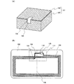
図1(A)に、本発明のIDタグ100を用いて容器101の蓋102を封印している様子を示す。容器101は、蓋102と本体107とを有している。IDタグ100を剥離しない限り、容器101の蓋102を開けることができないような位置にIDタグ100を貼り合わせることで、IDタグ100が貼られた後に蓋102が開けられたか否かを確実に把握することができる。破線106は、容器101の蓋102と本体107との境目を示している。
FIG. 1A shows a state where the
図1(B)に、IDタグ100の一形態を示す。IDタグ100は、支持体103と、支持体103に形成されたアンテナ104と、薄膜集積回路105とを有している。破線106は、容器101の蓋102と本体107との境目を示している。配線108はアンテナ104の一部に相当し、配線108によりアンテナ104の端子109、110間を電気的に接続することができる。
FIG. 1B illustrates one mode of the
薄膜集積回路105は、アンテナ104において生じた交流の電気信号から電源電圧または各種信号を生成し、該電源電圧、各種信号を用いて各種動作を行なうことができる。そして、薄膜集積回路105において生成した交流の電気信号がアンテナ104に入力され、アンテナ104からリーダ/ライタに各種信号が送られる。
The thin film integrated
次に図1(B)に示したIDタグ100の、破線111で囲まれた領域の拡大図を、図2(A)に示す。また図2(A)のA−A’における断面図を図2(B)に示す。なお図2(B)では、薄膜集積回路105としてTFT112、113の断面図を示しているが、本発明のIDタグにおいて薄膜集積回路105に含まれる半導体素子はTFTに限られない。例えばTFTの他に、記憶素子、ダイオード、光電変換素子、抵抗素子、コイル、容量素子、インダクタなどの、その他の半導体素子が用いられていても良い。
Next, an enlarged view of a region surrounded by a
支持体103は、薄膜集積回路105及びアンテナ104が形成されている側とは反対の面に接着剤114が塗布されている。接着剤114は、IDタグの支持体を、対象物に貼り合わせることができる物質であれば良い。なお、支持体103の一部が接着剤として機能させても良い。或いは、接着剤を敢えて塗布せず、貼り合わせる際に別途用意した接着剤を用いるようにしても良い。
The
そして本発明のIDタグでは、薄膜集積回路105が有する半導体素子、図2(B)ではTFT112、113、と、アンテナ104との間に、分離層115が形成されている。なお薄膜集積回路105とアンテナ104とは、重なっていても良いし、重なっていなくとも良い。そしてアンテナ104とTFT112、TFT113とを電気的に接続するための配線116は、分離層115を貫通するように形成されている。なお配線116は、アンテナ104の一部であっても良いし、別途形成された配線であっても良い。
In the ID tag of the present invention, the
なお図2(B)では、薄膜集積回路105とアンテナ104との間に分離層115が形成されている例を示しているが、本発明はこの構成に限定されない。アンテナ104と薄膜集積回路105とを電気的に接続するための配線116が、分離層115を貫通するように形成されていれば良い。或いは、アンテナ104を構成している配線が、分離層115を貫通するように形成されていれば良い。或いは、薄膜集積回路105を構成している半導体素子どうしを電気的に接続している配線が、分離層115を貫通するように形成されていれば良い。
Note that FIG. 2B illustrates an example in which the
図2(B)に示したIDタグを対象物120に貼り合わせている様子を、図3(A)に示す。次に図3(A)に示したIDタグを、物理的な力を用いて、分離層115を境に引き剥がしている様子を図3(B)に示す。図3(B)に示すように、分離層115を境にIDタグの一部が引き剥がされることで、分離層115を貫通している配線116を切断することができる。よって、アンテナ104と薄膜集積回路105とを電気的に分離させることができ、IDタグとリーダ/ライタとの間における信号または電源電圧の送受を制限することができる。
FIG. 3A shows a state where the ID tag shown in FIG. Next, FIG. 3B shows a state where the ID tag shown in FIG. 3A is peeled off with the
なお図1に示したような、蓋102が開けられたか否かを把握するために用いるIDタグ100は、IDタグ100を引き剥がすことで切断される配線を少なくとも2つの箇所に形成する。そして該2つの箇所は、破線106に示す容器101の蓋102と本体107との境目を間に挟んで存在していることが望ましい。上記構成により、蓋102を開けるためには2箇所の配線のうち少なくとも1箇所の配線を切断しなければならなくなり、確実に蓋102が開けられたか否かを把握することができる。
Note that the
なお図1では、IDタグを用いて容器を封印しているが、封印するのは、口を閉じることができる入れ物であれば良い。 In FIG. 1, the container is sealed using the ID tag, but the container may be sealed as long as it can close the mouth.
また本発明のIDタグの用途は、入れ物の封印のみに限定されない。一度IDタグを剥がすと、剥がしたという事実を把握することができるという特徴を生かして、IDタグを剥離すると対象物が有する効力を無効にしたり、価値を低減させたりするという用途にも用いることができる。例えば、荷札、値札、名札など、対象物の情報を有するタグに貼り合わせても良いし、本発明のIDタグ自体をタグとして用いても良い。また例えば、戸籍謄本、住民票、パスポート、免許証、身分証、会員証、鑑定書、クレジットカード、キャッシュカード、プリペイドカード、診察券、定期券など、事実を証明する文書に相当する証書に貼り合わせても良い。また例えば、手形、小切手、貨物引換証、船貨証券、倉庫証券、株券、債券、商品券、抵当証券など、私法上の財産権を表示する証券に相当する有価証券に貼り合わせても良い。 Moreover, the use of the ID tag of the present invention is not limited only to the sealing of containers. Take advantage of the fact that once the ID tag is peeled off, the fact that it has been peeled off can be used to invalidate the effectiveness of the object or reduce its value when the ID tag is peeled off. Can do. For example, it may be attached to a tag having information on an object such as a tag, price tag, or name tag, or the ID tag itself of the present invention may be used as a tag. Also, for example, a certificate equivalent to a document proving the fact, such as a certified copy of a family register, resident's card, passport, license, identification card, membership card, certificate, credit card, cash card, prepaid card, examination ticket, commuter pass, etc. May be combined. For example, it may be attached to securities corresponding to securities displaying private property rights such as bills, checks, freight exchange certificates, cargo securities, warehouse securities, stock certificates, bonds, gift certificates, mortgage securities.
図4(A)に、封筒を封印するために本発明のIDタグを用いる例を示す。図4(A)では、本発明のIDタグ402を貼り合わせることで、封筒401の入り口を閉じている。上記構成により、宛名に記載された人物が封筒を開封する前に、第三者によって開封されたか否かを把握することができる。
FIG. 4A shows an example in which the ID tag of the present invention is used to seal an envelope. In FIG. 4A, the entrance of the
図4(B)に、本発明のIDタグ410が貼り合わされた小切手411の一例を示す。図4(B)では、IDタグ410が小切手411の表面に貼り合わされている。上記構成により、例えば偽造を目的としてIDタグ410を剥がしても、剥がしたことを後に把握することができるので、小切手411を無効とすることができる。
FIG. 4B shows an example of a
図4(C)に、本発明のIDタグ420を有するパスポート421の一例を示す。図13(A)では、IDタグ420がパスポート421の表紙に取り付けられているが、パスポート421が有する他のページに取り付けられていても良い。上記構成により、例えば偽造を目的としてIDタグ420を剥がしても、剥がしたことを後に把握することができるので、パスポート421を無効とすることができる。
FIG. 4C shows an example of a
次に、本発明の半導体装置の作製方法について説明する。なお本実施の形態では、半導体素子として絶縁分離されたTFTを例示するが、薄膜集積回路に含まれる半導体素子はこれに限定されず、あらゆる回路素子を用いることができる。例えば、TFTの他に、記憶素子、ダイオード、光電変換素子、抵抗素子、コイル、容量素子、インダクタなどが代表的に挙げられる。 Next, a method for manufacturing a semiconductor device of the present invention will be described. Note that in this embodiment, an isolated TFT is exemplified as a semiconductor element; however, a semiconductor element included in a thin film integrated circuit is not limited to this, and any circuit element can be used. For example, in addition to the TFT, a memory element, a diode, a photoelectric conversion element, a resistance element, a coil, a capacitor element, an inductor, and the like can be typically given.
まず図5(A)に示すように、スパッタ法を用いて基板500上に剥離層501を成膜する。基板500として、例えばバリウムホウケイ酸ガラスや、アルミノホウケイ酸ガラスなどのガラス基板、石英基板、SUS基板等、後の作製工程における処理温度に耐え得る基板を用いることができる。
First, as illustrated in FIG. 5A, a
剥離層501は、非晶質シリコン、多結晶シリコン、単結晶シリコン、微結晶シリコン(セミアモルファスシリコンを含む)等、シリコンを主成分とする層を用いることができる。剥離層は、スパッタ法、プラズマCVD法等を用いて形成することができる。本実施の形態では、膜厚500nm程度の非晶質シリコンをスパッタ法で形成し、剥離層501として用いる。
As the
次に、剥離層501上に下地膜502を形成する。下地膜502は、後に半導体素子を支持体上に接着剤で貼り合わせた際に、支持体や接着剤中に含まれるNaなどのアルカリ金属やアルカリ土類金属が、半導体素子に用いられている半導体膜中に拡散し、半導体素子の特性に悪影響を及ぼすのを防ぐために形成する。また下地膜502は、剥離層501をエッチングする際、エッチャントから半導体素子を保護する役割も有する。よってアルカリ金属やアルカリ土類金属の半導体膜への拡散を抑えることができ、なおかつシリコンのエッチングに用いられるエッチャントから半導体素子を保護することができる酸化珪素、窒化珪素、窒化酸化珪素などの絶縁膜を用いて形成することが望ましい。本実施の形態では、プラズマCVD法を用いて窒化酸化珪素膜を10nm〜400nm(好ましくは50nm〜300nm)の膜厚になるように成膜する。なお下地膜502は単層の絶縁膜であっても複数の絶縁膜を積層したものであっても良い。
Next, a
次に、下地膜502上に半導体膜を形成する。半導体膜は、下地膜502を形成した後、大気に曝さずに形成することが望ましい。半導体膜の膜厚は20〜200nm(好ましくは40〜170nm)とする。なお半導体膜は、非晶質半導体であっても良いし、セミアモルファス半導体であっても良いし、多結晶半導体であっても良い。また半導体は珪素だけではなくシリコンゲルマニウムも用いることができる。シリコンゲルマニウムを用いる場合、ゲルマニウムの濃度は0.01〜4.5atomic%程度であることが好ましい。
Next, a semiconductor film is formed over the
なお半導体膜は、公知の技術により結晶化しても良い。公知の結晶化方法としては、電熱炉を使用した熱結晶化方法、レーザ光を用いたレーザ結晶化法、赤外光を用いたランプアニール結晶化法がある。或いは、触媒元素を用いる結晶化法を用いることもできる。例えばレーザ結晶化を用いる場合、レーザ結晶化の前に、レーザに対する半導体膜の耐性を高めるために、500℃、1時間の熱アニールを該半導体膜に対して行なう。そして連続発振が可能な固体レーザを用い、基本波の第2高調波〜第4高調波のレーザ光を照射することで、大粒径の結晶を得ることができる。例えば、代表的には、Nd:YVO4レーザ(基本波1064nm)の第2高調波(532nm)や第3高調波(355nm)を用いるのが望ましい。具体的には、連続発振のYVO4レーザから射出されたレーザ光を非線形光学素子により高調波に変換し、出力10Wのレーザ光を得る。そして、好ましくは光学系により照射面にて矩形状または楕円形状のレーザ光に成形して、半導体膜に照射する。このときのエネルギー密度は0.01〜100MW/cm2程度(好ましくは0.1〜10MW/cm2)が必要である。そして、走査速度を10〜2000cm/sec程度とし、照射する。 Note that the semiconductor film may be crystallized by a known technique. Known crystallization methods include a thermal crystallization method using an electric furnace, a laser crystallization method using laser light, and a lamp annealing crystallization method using infrared light. Alternatively, a crystallization method using a catalytic element can be used. For example, when laser crystallization is used, before laser crystallization, thermal annealing is performed on the semiconductor film at 500 ° C. for 1 hour in order to increase the resistance of the semiconductor film to the laser. By using a solid-state laser capable of continuous oscillation and irradiating laser light of the second harmonic to the fourth harmonic of the fundamental wave, a crystal having a large grain size can be obtained. For example, typically, it is desirable to use the second harmonic (532 nm) or the third harmonic (355 nm) of an Nd: YVO 4 laser (fundamental wave 1064 nm). Specifically, laser light emitted from a continuous wave YVO 4 laser is converted into a harmonic by a non-linear optical element to obtain laser light with an output of 10 W. Then, it is preferably formed into a rectangular or elliptical laser beam on the irradiation surface by an optical system and irradiated onto the semiconductor film. At this time, the energy density of approximately 0.01 to 100 MW / cm 2 (preferably 0.1 to 10 MW / cm 2) is required. Then, irradiation is performed at a scanning speed of about 10 to 2000 cm / sec.
また、パルス発振のレーザ光の発振周波数を10MHz以上とし、通常用いられている数十Hz〜数百Hzの周波数帯よりも著しく高い周波数帯を用いてレーザ結晶化を行なっても良い。パルス発振でレーザ光を半導体膜に照射してから半導体膜が完全に固化するまでの時間は数十nsec〜数百nsecと言われている。よって上記周波数帯を用いることで、半導体膜がレーザ光によって溶融してから固化するまでに、次のパルスのレーザ光を照射できる。したがって、半導体膜中において固液界面を連続的に移動させることができるので、走査方向に向かって連続的に成長した結晶粒を有する半導体膜が形成される。具体的には、含まれる結晶粒の走査方向における幅が10〜30μm、走査方向に対して垂直な方向における幅が1〜5μm程度の結晶粒の集合を形成することができる。該走査方向に沿って長く延びた単結晶の結晶粒を形成することで、少なくともTFTのチャネル方向には結晶粒界のほとんど存在しない半導体膜の形成が可能となる。 Alternatively, laser crystallization may be performed using a frequency band that is significantly higher than a frequency band of several tens to several hundreds Hz that is normally used, with an oscillation frequency of pulsed laser light of 10 MHz or higher. It is said that the time from irradiating a semiconductor film with laser light by pulse oscillation until the semiconductor film is completely solidified is several tens to several hundreds nsec. Therefore, by using the above frequency band, it is possible to irradiate the next pulse of laser light from when the semiconductor film is melted by the laser light to solidification. Accordingly, since the solid-liquid interface can be continuously moved in the semiconductor film, a semiconductor film having crystal grains continuously grown in the scanning direction is formed. Specifically, a set of crystal grains having a width of 10 to 30 μm in the scanning direction of the included crystal grains and a width of about 1 to 5 μm in a direction perpendicular to the scanning direction can be formed. By forming single crystal grains extending long along the scanning direction, it is possible to form a semiconductor film having almost no crystal grain boundaries in at least the channel direction of the TFT.
なおレーザ結晶化は、連続発振の基本波のレーザ光と連続発振の高調波のレーザ光とを並行して照射するようにしても良いし、連続発振の基本波のレーザ光とパルス発振の高調波のレーザ光とを並行して照射するようにしても良い。 Laser crystallization may be performed by irradiating a continuous-wave fundamental laser beam and a continuous-wave harmonic laser beam in parallel, or a continuous-wave fundamental laser beam and a pulse oscillation harmonic. You may make it irradiate with the laser beam of a wave in parallel.
なお、希ガスや窒素などの不活性ガス雰囲気中でレーザ光を照射するようにしても良い。これにより、レーザ光照射による半導体表面の荒れを抑えることができ、界面準位密度のばらつきによって生じる閾値のばらつきを抑えることができる。 Note that laser light may be irradiated in an inert gas atmosphere such as a rare gas or nitrogen. Thereby, roughness of the semiconductor surface due to laser light irradiation can be suppressed, and variation in threshold value caused by variation in interface state density can be suppressed.
上述した半導体膜へのレーザ光の照射により、結晶性がより高められた半導体膜が形成される。なお、予め多結晶半導体を、スパッタ法、プラズマCVD法、熱CVD法などで形成するようにしても良い。 By irradiating the above-described semiconductor film with laser light, a semiconductor film with higher crystallinity is formed. Note that a polycrystalline semiconductor may be formed in advance by a sputtering method, a plasma CVD method, a thermal CVD method, or the like.
また本実施の形態では半導体膜を結晶化しているが、結晶化せずに非晶質珪素膜または微結晶半導体膜のまま、後述のプロセスに進んでも良い。非晶質半導体、微結晶半導体を用いたTFTは、多結晶半導体を用いたTFTよりも作製工程が少ない分、コストを抑え、歩留まりを高くすることができるというメリットを有している。 Further, although the semiconductor film is crystallized in this embodiment mode, the process may proceed to a process to be described later while the amorphous silicon film or the microcrystalline semiconductor film is not crystallized. A TFT using an amorphous semiconductor or a microcrystalline semiconductor has an advantage that a manufacturing cost can be reduced and a yield can be increased because the number of manufacturing steps is smaller than that of a TFT using a polycrystalline semiconductor.
なおセミアモルファス半導体とは、非晶質半導体と結晶構造を有する半導体(単結晶、多結晶を含む)の中間的な構造の半導体を含む膜である。このセミアモルファス半導体は、自由エネルギー的に安定な第3の状態を有する半導体であって、短距離秩序を持ち格子歪みを有する結晶質なものであり、その粒径を0.5〜20nmとして非単結晶半導体中に分散させて存在せしめることが可能である。セミアモルファス半導体は、そのラマンスペクトルが520cm-1よりも低波数側にシフトしており、またX線回折ではSi結晶格子に由来するとされる(111)、(220)の回折ピークが観測される。また、未結合手(ダングリングボンド)の中和剤として水素またはハロゲンを少なくとも1原子%またはそれ以上含ませている。ここでは便宜上、このような半導体をセミアモルファス半導体(SAS)と呼ぶ。さらに、ヘリウム、アルゴン、クリプトン、ネオンなどの希ガス元素を含ませて格子歪みをさらに助長させることで安定性が増し良好なセミアモルファス半導体が得られる。 Note that a semi-amorphous semiconductor is a film including a semiconductor having an intermediate structure between an amorphous semiconductor and a semiconductor having a crystal structure (including single crystal and polycrystal). This semi-amorphous semiconductor is a semiconductor having a third state which is stable in terms of free energy, and is a crystalline one having a short-range order and having a lattice strain, and having a grain size of 0.5 to 20 nm. It can be dispersed in a single crystal semiconductor. The semi-amorphous semiconductor has its Raman spectrum shifted to a lower wavenumber than 520 cm −1 , and diffraction peaks of (111) and (220), which are considered to be derived from the Si crystal lattice in X-ray diffraction, are observed. . Further, hydrogen or halogen is contained at least 1 atomic% or more as a neutralizing agent for dangling bonds. Here, for convenience, such a semiconductor is referred to as a semi-amorphous semiconductor (SAS). Further, by adding a rare gas element such as helium, argon, krypton, or neon to further promote lattice distortion, stability is improved and a good semi-amorphous semiconductor can be obtained.
次に、図5(A)に示すように半導体膜をパターニングし、島状の半導体膜503、半導体膜504を形成する。そして図5(B)に示すように、該島状の半導体膜503、504を用いてTFTに代表される各種の半導体素子を形成する。なお図5(B)では、下地膜502と島状の半導体膜503、504とが接しているが、半導体素子によっては、下地膜502と島状の半導体膜503、504との間に、電極や絶縁膜等が形成されていても良い。例えば半導体素子の1つであるボトムゲート型のTFTの場合、下地膜502と島状の半導体膜503、504との間に、ゲート電極とゲート絶縁膜が形成される。
Next, as shown in FIG. 5A, the semiconductor film is patterned to form island-shaped
図5(B)では、島状の半導体膜503、504を用いてトップゲート型のTFT505、TFT506を形成する。具体的には、島状の半導体膜503、504を覆うようにゲート絶縁膜507を形成し、ゲート絶縁膜507上に導電膜を成膜し、パターニングすることで、ゲート電極508、ゲート電極509を形成する。そして、ゲート電極508、509や、あるいはレジストを成膜しパターニングしたものをマスクとして用い、島状の半導体膜503、504にn型を付与する不純物を添加し、ソース領域、ドレイン領域、さらにはLDD領域等を形成する。なおここではTFT505、506を共にn型とするが、p型のTFTの場合は、p型の導電性を付与する不純物を添加する。上記一連の工程によってTFT505、506を形成することができる。
In FIG. 5B,
なお、ゲート絶縁膜507を形成した後、3〜100%の水素を含む雰囲気中で、300〜450℃で1〜12時間の熱処理を行ない、島状の半導体膜503、504を水素化する工程を行なっても良い。また、水素化の他の手段として、プラズマ水素化(プラズマにより励起された水素を用いる)を行っても良い。この水素化の工程により、熱的に励起された水素によりダングリングボンドを終端することができる。また、後の工程において可撓性を有する支持体上に半導体素子を貼り合わせた後、支持体を曲げることにより半導体膜中に欠陥が形成されたとしても、水素化により半導体膜中の水素の濃度を、1×10¹⁹〜5×10²¹atoms/cm3とすることで、半導体膜に含まれている水素によって該欠陥を終端させることができる。また該欠陥を終端させるために、半導体膜中にハロゲンを含ませておいても良い。
Note that after the
なおTFTの作製方法は上述した構成に限定されない。 Note that a method for manufacturing a TFT is not limited to the above-described structure.
次にTFT505、506を覆って、第1の層間絶縁膜510を形成する。そして、ゲート絶縁膜507及び第1の層間絶縁膜510にコンタクトホールを形成した後、コンタクトホールを介してTFT505、506と接続する配線511〜514を、第1の層間絶縁膜510に接するように形成する。
Next, a first
次に図5(C)に示すように、配線511〜514を覆うように、第1の層間絶縁膜510上に第2の層間絶縁膜515を形成する。そして、第2の層間絶縁膜515上に金属膜516を形成する。ここでは金属膜516にタングステンを用い、膜厚を10nm〜200nm、好ましくは50nm〜75nmとする。なお金属膜516は、後にアンテナと電気的に接続するための配線511、514と重なる領域に、開口部を形成しておく。
Next, as illustrated in FIG. 5C, a second
そして図5(D)に示すように、金属膜516の形成後、大気に曝すことなく絶縁膜を構成する酸化物膜517を、積層するように成膜する。ここでは酸化物膜517として酸化珪素膜を膜厚150nm〜300nmとなるように成膜する。なお、スパッタ法を用いる場合、基板500の端面にも成膜が施される。そのため、後の工程における剥離の際に、酸化物膜517が基板500側に残ってしまうのを防ぐために、端面に成膜された金属膜516と酸化物膜517とをO2アッシングなどで選択的に除去することが好ましい。
Then, as illustrated in FIG. 5D, after the
また酸化物膜517の成膜の際に、スパッタの前段階としてターゲットと基板との間をシャッターで遮断してプラズマを発生させる、プレスパッタを行なう。プレスパッタはArを10sccm、O2をそれぞれ30sccmの流量とし、基板500の温度を270℃、成膜パワーを3kWの平行状態に保って行なう。プレスパッタにより、金属膜516と酸化物膜517の間に極薄い数nm(ここでは3nm)程度の分離層(本実施の形態では金属酸化膜を用いる)518が形成される。金属酸化膜518は、金属膜516の表面が酸化することで形成される。よって図5(D)では、金属酸化膜518は酸化タングステンで形成される。
Further, when the
なお図5(D)では、プレスパッタにより金属酸化膜518を形成しているが、本発明はこれに限定されない。例えば酸素、または酸素にAr等の不活性ガスを添加し、プラズマにより意図的に金属膜516の表面を酸化し、金属酸化膜518を形成するようにしても良い。
In FIG. 5D, the
なお、第1の層間絶縁膜510、第2の層間絶縁膜515として、有機樹脂膜、無機絶縁膜、シロキサン系材料を出発材料として形成されたSi−O−Si結合を含む絶縁膜(以下、シロキサン系絶縁膜と呼ぶ)等を用いることができる。シロキサン系絶縁膜は、置換基に水素の他、フッ素、アルキル基、または芳香族炭化水素のうち少なくとも1種を有していても良い。
Note that as the first
次に、加熱処理を施すことで金属酸化膜518を結晶化する。結晶化により、金属酸化膜518が粒界において割れやすくなり、脆性を高めることができる。本実施の形態では金属酸化膜518として酸化タングステンが用いられており、この場合、金属酸化膜518の結晶化は420℃〜550℃、0.5〜5時間程度の加熱処理が望ましい。なお本実施の形態では、金属酸化膜518を結晶化するためだけに加熱処理の工程を設けているが、本発明はこの構成に限定されない。後に別の工程において加熱処理が行なわれる場合、後の工程の加熱処理がこの金属酸化膜の結晶化の工程を兼ねていても良い。また本実施の形態では酸化タングステンを用いている例を示しているので、金属酸化膜518を結晶化する工程を設けているが、本発明はこの構成に限定されない。金属酸化膜の脆性が十分に高い場合、必ずしも金属酸化膜518を結晶化するための工程を設けなくとも良い。
Next, the
次に図5(E)に示すように、金属膜516の開口部において第2の層間絶縁膜515及び酸化物膜517をエッチングし、配線511、514を一部露出させる。なお、第2の層間絶縁膜515と酸化物膜517とを同じ材料を用いて形成することで、上記エッチングの工程を簡略化することができる。
Next, as shown in FIG. 5E, the second
次に第3の層間絶縁膜520を形成する。第3の層間絶縁膜520は有機樹脂膜、無機絶縁膜またはシロキサン系絶縁膜を用いることができる。第3の層間絶縁膜520は、配線511、514が一部露出する様な位置に開口部を有するように形成する。
Next, a third
次に図6(A)に示すように、第3の層間絶縁膜520上にアンテナ519を形成する。アンテナ519は、Ag、Au、Cu、Pd、Cr、Mo、Ti、Ta、W、Alなどの金属、金属化合物を1つまたは複数有する導電材料を用いることができる。アンテナ519の一部は、金属酸化膜518を貫通している。そしてアンテナ519は、配線511、514と接続されている。なお図6(A)では、アンテナ519が配線511、514と直接接続されているが、本発明のIDタグはこの構成に限定されない。例えば別途形成した配線を用いて、アンテナ519と配線511、514とを電気的に接続するようにしても良い。
Next, as illustrated in FIG. 6A, an
アンテナ519は印刷法、フォトリソグラフィ法、蒸着法または液滴吐出法などを用いて形成することができる。本実施の形態では、アンテナ519が単層の導電膜で形成されているが、複数の導電膜が積層されたアンテナ519を形成することも可能である。
The
なお液滴吐出法とは、所定の組成物を含む液滴を細孔から吐出して所定のパターンを形成する方法を意味し、インクジェット法などがその範疇に含まれる。また印刷法にはスクリーン印刷法、オフセット印刷法などが含まれる。印刷法、液滴吐出法を用いることで、露光用のマスクを用いずとも、アンテナ519を形成することが可能になる。また、液滴吐出法、印刷法だと、フォトリソグラフィ法と異なり、エッチングにより除去されてしまうような材料の無駄がない。また高価な露光用のマスクを用いなくとも良いので、IDタグの作製に費やされるコストを抑えることができる。
The droplet discharge method means a method of forming a predetermined pattern by discharging droplets containing a predetermined composition from the pores, and includes an ink jet method and the like in its category. The printing method includes a screen printing method and an offset printing method. By using a printing method or a droplet discharge method, the
液滴吐出法または各種印刷法を用いる場合、例えば、CuをAgでコートした導電粒子なども用いることが可能である。なお液滴吐出法を用いてアンテナ519を形成する場合、該アンテナ519の密着性が高まるような処理を、第3の層間絶縁膜520の表面に施すことが望ましい。
In the case of using a droplet discharge method or various printing methods, for example, conductive particles in which Cu is coated with Ag can be used. Note that in the case where the
密着性を高めることができる方法として、具体的には、例えば触媒作用により導電膜または絶縁膜の密着性を高めることができる金属または金属化合物を第3の層間絶縁膜520の表面に付着させる方法、形成される導電膜または絶縁膜との密着性が高い有機系の絶縁膜、金属、金属化合物を第3の層間絶縁膜520の表面に付着させる方法、第3の層間絶縁膜520の表面に大気圧下または減圧下においてプラズマ処理を施し、表面改質を行なう方法などが挙げられる。また、上記導電膜または絶縁膜との密着性が高い金属として、チタン、チタン酸化物の他、3d遷移元素であるSc、Ti、V、Cr、Mn、Fe、Co、Ni、Cu、Znなどが挙げられる。また金属化合物として、上述した金属の酸化物、窒化物、酸窒化物などが挙げられる。上記有機系の絶縁膜として、例えばポリイミド、シロキサン系絶縁膜等が挙げられる。
As a method for improving the adhesion, specifically, for example, a method of attaching a metal or a metal compound capable of enhancing the adhesion of the conductive film or the insulating film to the surface of the third
第3の層間絶縁膜520に付着させる金属または金属化合物が導電性を有する場合、アンテナの正常な動作が妨げられないように、そのシート抵抗を制御する。具体的には、導電性を有する金属または金属化合物の平均の厚さを、例えば1〜10nmとなるように制御したり、該金属または金属化合物を酸化により部分的に、または全体的に絶縁化したりすれば良い。或いは、密着性を高めたい領域以外は、付着した金属または金属化合物をエッチングにより選択的に除去しても良い。また金属または金属化合物を、予め基板の全面に付着させるのではなく、液滴吐出法、印刷法、ゾル−ゲル法などを用いて特定の領域にのみ選択的に付着させても良い。なお金属または金属化合物は、第3の層間絶縁膜520の表面において完全に連続した膜状である必要はなく、ある程度分散した状態であっても良い。
When the metal or metal compound attached to the third
そしてアンテナ519を形成した後、アンテナ519を覆うように、第3の層間絶縁膜520上に保護層521を形成する。保護層521は、後に剥離層501をエッチングにより除去する際に、アンテナ519を保護することができる材料を用いる。例えば、水またはアルコール類に可溶なエポキシ系、アクリレート系、シリコン系の樹脂を全面に塗布することで保護層521を形成することができる。
After the
本実施の形態では、スピンコート法で水溶性樹脂(東亜合成製:VL−WSHL10)を膜厚30μmとなるように塗布し、仮硬化させるために2分間の露光を行ったあと、UV光を裏面から2.5分、表面から10分、合計12.5分の露光を行って本硬化させて、保護層521を形成する。なお、複数の有機樹脂を積層する場合、有機樹脂同士では使用している溶媒によって塗布または焼成時に一部溶解したり、密着性が高くなりすぎたりする恐れがある。従って、第3の層間絶縁膜520と保護層521を共に同じ溶媒に可溶な有機樹脂を用いる場合、後の工程において保護層521の除去がスムーズに行なわれるように、第3の層間絶縁膜520を覆うように、無機絶縁膜(SiNX膜、SiNXOY膜、AlNX膜、またはAlNXOY膜)を形成しておくことが好ましい。
In the present embodiment, a water-soluble resin (manufactured by Toagosei Co., Ltd .: VL-WSHL10) is applied by spin coating so as to have a film thickness of 30 μm, and after exposure for 2 minutes for temporary curing, UV light is applied. Exposure is performed for 2.5 minutes from the back surface and 10 minutes from the front surface for a total of 12.5 minutes to perform main curing to form the
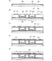
次に図6(B)に示すように、薄膜集積回路どうしを分離するために溝522を形成する。溝522は、剥離層501が露出する程度であれば良い。溝522の形成は、ダイシング、スクライビングなどを用いることができる。なお、基板500上に形成されている薄膜集積回路を分離する必要がない場合、必ずしも溝522を形成する必要はない。
Next, as shown in FIG. 6B, a
次に図6(C)に示すように、剥離層501をエッチングにより除去する。本実施の形態では、エッチングガスとしてハロゲン化フッ素を用い、該ガスを溝522から導入する。本実施の形態では、例えばClF3(三フッ化塩素)を用い、温度:350℃、流量:300sccm、気圧:6Torr、時間:3hの条件で行う。また、ClF3ガスに窒素を混ぜたガスを用いても良い。ClF3等のハロゲン化フッ素を用いることで、剥離層501が選択的にエッチングされ、基板500をTFT505、506から剥離することができる。
Next, as shown in FIG. 6C, the
なおハロゲン化フッ素は、気体であっても液体であってもどちらでも良い。 The halogenated fluorine may be a gas or a liquid.
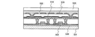
次に図7に示すように、剥離されたTFT505、506及びアンテナ519を、接着剤530を用いて支持体531に貼り合わせる。接着剤530は、支持体531と下地膜502とを貼り合わせることができる材料を用いる。さらに接着剤530は、完成したIDタグを対象物に貼り合わせた後に引き剥がす際に、IDタグが金属酸化膜518において引き剥がされることはあっても、支持体531と下地膜502とが引き剥がされることはない程度の強度を有する材料を用いる。接着剤530は、例えば反応硬化型接着剤、熱硬化型接着剤、紫外線硬化型接着剤等の光硬化型接着剤、嫌気型接着剤などの各種硬化型接着剤を用いることができる。
Next, as shown in FIG. 7, the peeled
支持体531として、フレキシブルな紙またはプラスチックなどの有機材料を用いることができる。または支持体531として、フレキシブル無機材料を用いていても良い。プラスチック基板は、極性基のついたポリノルボルネンからなるARTON(JSR製)を用いることができる。また、ポリエチレンテレフタレート(PET)に代表されるポリエステル、ポリエーテルスルホン(PES)、ポリエチレンナフタレート(PEN)、ポリカーボネート(PC)、ナイロン、ポリエーテルエーテルケトン(PEEK)、ポリスルホン(PSF)、ポリエーテルイミド(PEI)、ポリアリレート(PAR)、ポリブチレンテレフタレート(PBT)、ポリイミド、アクリロニトリルブタジエンスチレン樹脂、ポリ塩化ビニル、ポリプロピレン、ポリ酢酸ビニル、アクリル樹脂などが挙げられる。支持体531は薄膜集積回路において発生した熱を拡散させるために、2〜30W/mK程度の高い熱伝導率を有するのが望ましい。
As the
また図7に示すように、保護層521を除去した後、アンテナ519を覆うように接着剤532を第3の層間絶縁膜520上に塗布し、カバー材533を貼り合わせる。カバー材533は支持体531と同様に、フレキシブルな紙またはプラスチックなどの有機材料を用いることができる。また接着剤532は、カバー材533と第3の層間絶縁膜520及びアンテナ519とを貼り合わせることができる材料を用いる。さらに接着剤532は、完成した半導体装置を対象物に貼り合わせた後に引き剥がす際に、半導体装置が金属酸化膜518において引き剥がされることはあっても、カバー材533と第3の層間絶縁膜520及びアンテナ519とが引き剥がされることはない程度の強度を有する有機樹脂または無機材料を用いる。接着剤532は、例えば反応硬化型接着剤、熱硬化型接着剤、紫外線硬化型接着剤等の光硬化型接着剤、嫌気型接着剤などの各種硬化型接着剤を用いることができる。
Further, as shown in FIG. 7, after the
上述した各工程を経て、本発明の半導体装置が完成する。上記作製方法によって、トータルの膜厚0.3μm以上3μm以下、代表的には2μm程度の飛躍的に薄い薄膜集積回路を支持体531とカバー材533との間に形成することができる。なお薄膜集積回路の厚さは、半導体素子自体の厚さのみならず、接着剤530と接着剤532間に形成された各種絶縁膜及び層間絶縁膜の厚さを含めるものとする。また半導体装置が有する薄膜集積回路の占める面積を、5mm四方以下、より望ましくは0.3mm四方〜4mm四方程度とすることができる。
Through the above-described steps, the semiconductor device of the present invention is completed. By the above manufacturing method, a remarkably thin thin film integrated circuit having a total film thickness of 0.3 μm to 3 μm, typically about 2 μm, can be formed between the
なお薄膜集積回路を、支持体531とカバー材533の間のより中央に位置させることで、半導体装置の機械的強度を高めることができる。具体的には、支持体531とカバー材533の間の距離をdとすると、支持体531と、薄膜集積回路の厚さ方向における中心との距離xが、以下の式1を満たすように、接着剤530、532の厚さを制御することが望ましい。
Note that the mechanical strength of the semiconductor device can be increased by positioning the thin film integrated circuit at a more central position between the

なお本実施の形態では、金属膜516としてWを用いる例について説明したが、本発明において金属膜はこの材料に限定されない。その表面に金属酸化膜518が形成され、該金属酸化膜518を境に半導体装置を部分的に引き剥がすことができるような金属を含む材料であれば良い。例えばWの他、TiN、WN、Mo等を用いることができる。またWを含めたこれら金属の合金を金属膜として用いる場合、その組成比によって金属酸化膜518を結晶化するための加熱処理の最適な温度が異なる。よって組成比を調整することで、半導体素子の作製工程にとって妨げとならない温度で加熱処理を行なうことができ、半導体素子のプロセスの選択肢が制限されにくい。
Note that although an example in which W is used for the
また上述した工程に加えて、金属酸化膜518と酸化物膜517の間の密着性、または金属酸化膜518と金属膜516の間の密着性を部分的に低下させ、剥離開始のきっかけとなる部分を形成する処理を行なっておいても良い。具体的には、剥離しようとする領域の周縁に沿って外部から局所的に圧力を加えて金属酸化膜518の層内または界面近傍の一部に損傷を与える。例えば、ダイヤモンドペンなどの硬い針を金属酸化膜518の端部近傍に垂直に押しつけ、そのまま荷重をかけた状態で金属酸化膜518に沿って動かせば良い。好ましくは、スクライバー装置を用い、押し込み量を0.1mm〜2mmとし、圧力をかけて動かせばよい。このように、剥離が開始されるきっかけとなるような、密着性の低下した部分を形成することで、半導体装置を対象物から引き剥がす際に、確実に金属酸化膜518の部分において半導体装置が引き剥がされるようにすることができる。
Further, in addition to the above-described steps, the adhesion between the
なお半導体装置に用いられる半導体膜や絶縁膜等に、シリアルナンバーを刻印しておけば、例えばROMにデータを記憶させる前のICカードが、盗難等により第三者に不正に渡ったとしても、シリアルナンバーからその流通のルートをある程度割り出すことが可能である。この場合、復元不可能な程度に半導体装置を分解しないと消せないような位置に、シリアルナンバーを刻印しておくとより効果的である。 If a serial number is engraved on a semiconductor film or an insulating film used in a semiconductor device, for example, even if an IC card before storing data in a ROM is illegally passed to a third party due to theft, The distribution route can be determined to some extent from the serial number. In this case, it is more effective to engrave the serial number at a position where the semiconductor device cannot be erased unless it is disassembled to such an extent that it cannot be restored.
次に、例えば図8(A)に示すように、図7に示した半導体装置の支持体531に、接着剤540を用いて対象物541を貼り合わせたとする。このとき接着剤540は、半導体装置を対象物541に貼り合わせた後に引き剥がす際に、半導体装置が金属酸化膜518において引き剥がされることはあっても、支持体531と対象物541とが引き剥がされることはない程度の強度を有する材料を用いる。接着剤540は、例えば反応硬化型接着剤、熱硬化型接着剤、紫外線硬化型接着剤等の光硬化型接着剤、嫌気型接着剤などの各種硬化型接着剤を用いることができる。
Next, for example, as illustrated in FIG. 8A, it is assumed that an object 541 is bonded to the
次に、図8(B)に示すように、半導体装置を引き剥がそうと力を加えると、金属酸化膜518が分離し、半導体装置が部分的に引き剥がされる。具体的にこの引き剥がしによって、金属膜516と金属酸化膜518の間で分離する部分と、酸化物膜517と金属酸化膜518の間で分離する部分と、金属酸化膜518自体が双方に分離する部分とが生じる。そして、支持体531側に半導体素子(ここではTFT505、506)が、またカバー材533側にアンテナ519が、それぞれ貼り付くように分離する。なおアンテナ519は、完全にカバー材533側に分離されていなくともよく、その一部が支持体531側に分離されていても良い。上記引き剥がしにより、アンテナ519とTFT505、506が電気的に分離され、IDタグとリーダ/ライタとの間における信号または電源電圧の送受を確実に制限することができる。
Next, as shown in FIG. 8B, when force is applied to peel off the semiconductor device, the
なお本実施の形態では、アンテナ519と、薄膜集積回路に含まれるTFT505、506との間に金属酸化膜518が形成されているが、本発明はこの構成に限定されない。アンテナ519を構成している配線が、金属酸化膜518を貫通するように形成されていれば良い。或いは、薄膜集積回路を構成している半導体素子どうしを電気的に接続している配線が、金属酸化膜518を貫通するように形成されていれば良い。或いは、アンテナ519と薄膜集積回路とを電気的に接続するための配線が、金属酸化膜518を貫通するように形成されていれば良い。
Note that although a
なお薄膜集積回路を基板500から剥離する方法は、本実施の形態で示したように珪素膜のエッチングを用いる方法に限定されず、他の様々な方法を用いることができる。例えば、剥離層をレーザ光の照射により破壊し、薄膜集積回路を基板から剥離することもできる。また例えば、薄膜集積回路が形成された基板を機械的に削除または溶液やガスによるエッチングで除去することで、薄膜集積回路を基板から剥離することもできる。
Note that the method for peeling the thin film integrated circuit from the
なお、TFT505、506を第1の層間絶縁膜510で覆う前に、別途、窒化珪素膜または窒化酸化珪素膜でTFT505、506を覆うようにしても良い。上記構成により、TFT505、506が下地膜502と上記窒化珪素膜または窒化酸化珪素膜とで覆われるため、Naなどのアルカリ金属やアルカリ土類金属が、半導体素子に用いられている半導体膜中に拡散し、半導体素子の特性に悪影響を及ぼすのをより防ぐことができる。
Note that the
また半導体装置の可撓性を確保するために、下地膜502に接する接着剤530に有機樹脂を用いる場合、下地膜502として窒化珪素膜または窒化酸化珪素膜を用いることで、有機樹脂からNaなどのアルカリ金属やアルカリ土類金属が半導体膜中に拡散するのを防ぐことができる。
In order to ensure flexibility of the semiconductor device, when an organic resin is used for the adhesive 530 in contact with the
また対象物の表面が曲面を有しており、それにより該曲面貼り合わされた半導体装置の支持体が、錐面、柱面など母線の移動によって描かれる曲面を有するように曲がってしまう場合、該母線の方向とTFTのキャリアが移動する方向とを揃えておくことが望ましい。上記構成により、支持体が曲がっても、それによってTFTの特性に影響が出るのを抑えることができる。また、島状の半導体膜が薄膜集積回路内において占める面積の割合を、5〜30%とすることで、支持体が曲がっても、それによってTFTの特性に影響が出るのをより抑えることができる。 Further, when the surface of the object has a curved surface, and the support of the semiconductor device bonded to the curved surface is bent so as to have a curved surface drawn by movement of a generatrix such as a cone surface or a column surface, It is desirable to align the direction of the bus and the direction in which the TFT carrier moves. With the above configuration, even if the support is bent, it can be suppressed that the characteristics of the TFT are affected thereby. Further, by setting the ratio of the area occupied by the island-shaped semiconductor film in the thin film integrated circuit to 5 to 30%, it is possible to further suppress the influence of the TFT characteristics even if the support is bent. it can.
本実施例では、1つの基板上に形成された複数の集積回路を剥離する際、形成される溝の形状について説明する。図9(A)に、溝901が形成された基板903の上面図を示す。また図9(B)に、図9(A)のA−A’における断面図を示す。
In this embodiment, a shape of a groove formed when a plurality of integrated circuits formed over one substrate is peeled will be described. FIG. 9A shows a top view of the
薄膜集積回路902は、剥離層904上に形成されており、剥離層904は基板903上に形成されている。溝901は各薄膜集積回路902の間に形成されており、なおかつ剥離層904が露出する程度の深さを有している。また本実施例では、複数の薄膜集積回路902は溝901によって完全にではなく部分的に分離されている。
The thin film integrated
次に図9(A)、図9(B)に示した溝901からエッチングガスを流し込み、剥離層904をエッチングにより除去した後の様子を、図9(C)、図9(D)に示す。図9(C)は、溝901が形成された基板903の上面図に相当し、図9(D)は、図9(C)のA−A’における断面図に相当する。エッチングにより溝901から破線905に示す領域まで、剥離層904のエッチングが進んだものとする。図9(C)、図9(D)に示すように、複数の薄膜集積回路902が、完全にではなく互いに一部繋がった状態で溝901により分離されていることで、剥離層904をエッチングした後に各薄膜集積回路902が支えをなくして移動してしまうのを防ぐことができる。
Next, an etching gas is supplied from the
図9(C)、図9(D)に示した状態まで形成したら、接着剤が付着したテープや、基板等を別途用意し、薄膜集積回路902を基板903から剥離する。そして剥離された複数の薄膜集積回路902は、互いに分断される前またはされた後に、支持体に貼りあわせられる。
After forming the state shown in FIGS. 9C and 9D, a tape or a substrate to which an adhesive is attached is separately prepared, and the thin film integrated
なお本実施例では、半導体装置の作製方法の一例を示しており、本発明の半導体装置の作製方法は本実施例で示した構成に限定されない。 Note that this embodiment shows an example of a method for manufacturing a semiconductor device, and the method for manufacturing a semiconductor device of the present invention is not limited to the structure shown in this embodiment.
次に図10を用いて、本発明の半導体装置の、機能的な構成の一形態について説明する。 Next, an example of a functional configuration of the semiconductor device of the present invention will be described with reference to FIG.
300はアンテナ、301は薄膜集積回路に相当する。アンテナ300は、アンテナコイル302と、アンテナコイル302内で形成される容量素子303とを有する。また薄膜集積回路301は、復調回路309、変調回路304、整流回路305、マイクロプロセッサ306、メモリ307、負荷をアンテナ300に与えるためのスイッチ308とを有している。なおメモリ307は1つに限定されず、複数であっても良い。
リーダ/ライタから電波として送られてきた信号は、アンテナコイル302において電磁誘導により交流の電気信号に変換される。復調回路309では該交流の電気信号を復調し、後段のマイクロプロセッサ306に送信する。また整流回路305では、交流の電気信号を用いて電源電圧を生成し、後段のマイクロプロセッサ306に供給する。
A signal transmitted as a radio wave from the reader / writer is converted into an AC electrical signal by electromagnetic induction in the
マイクロプロセッサ306では、入力された信号に従って各種演算処理を行なう。メモリ307にはマイクロプロセッサ306において用いられるプログラム、データなどが記憶されている他、演算処理時の作業エリアとしても用いることができる。そしてマイクロプロセッサ306から変調回路304に送られた信号は、交流の電気信号に変調される。スイッチ308は、変調回路304からの交流の電気信号に従って、アンテナコイル302に負荷を加えることができる。リーダ/ライタは、アンテナコイル302に加えられた負荷を電波で受け取ることで、結果的にマイクロプロセッサ306からの信号を読み取ることができる。
The
なお、図10に示す半導体装置は、本発明の一形態を示したのに過ぎず、本発明は上記構成に限定されない。信号の伝送方式は、図10に示したような電磁結合方式に限定されず、電磁誘導方式、マイクロ波方式やその他の伝送方式を用いていても良い。また例えばGPSなどの機能を有していても良い。 Note that the semiconductor device illustrated in FIG. 10 only shows one embodiment of the present invention, and the present invention is not limited to the above structure. The signal transmission method is not limited to the electromagnetic coupling method as shown in FIG. 10, and an electromagnetic induction method, a microwave method, or other transmission methods may be used. Moreover, you may have functions, such as GPS, for example.
本実施例では、薄膜集積回路内の半導体素子どうしを電気的に接続するための配線が、分離層を貫通している半導体装置の一例について説明する。図11(A)に、薄膜集積回路が有する半導体素子の1つであるTFT1101、1102と、アンテナ1103とが支持体1104上に貼りあわされている様子を示す。本実施例では、TFT1101、1102としてトップゲート型のTFTを用いている例を示している。
In this embodiment, an example of a semiconductor device in which a wiring for electrically connecting semiconductor elements in a thin film integrated circuit passes through an isolation layer will be described. FIG. 11A illustrates a state where
また図11(A)では、アンテナ1103を構成している配線と、TFT1101、1102のゲート電極1105、ゲート電極1106とが、同じ導電膜をパターニングすることで形成されている。そしてTFT1101とTFT1102とは、分離層(本実施例では金属酸化膜)1108を貫通している配線1107を用いて、電気的に接続されている。具体的には、配線1107と、TFT1101、1102にそれぞれ接続されている配線1110、1111とが、接続されている。
In FIG. 11A, the wiring that forms the
図11(B)に、図11(A)に示した半導体装置を対象物に貼り合わせた後、引き剥がしている様子を示す。図11(B)に示すように、金属酸化膜1108を境に半導体装置が引き裂かれることで、TFT1101とTFT1102とを電気的に接続している配線1107が切断されるので、よって薄膜集積回路の機能を破壊することができる。
FIG. 11B illustrates a state where the semiconductor device illustrated in FIG. 11A is attached to an object and then peeled off. As shown in FIG. 11B, the semiconductor device is torn between the
なお図11(B)では、IDタグの引き剥がしにより配線1107が切断される例を示したが、本実施例はこの構成に限定されない。例えば、半導体装置の引き剥がしにより、配線1107と、配線1110、1111とが切り離されるようにしても良い。
Note that FIG. 11B illustrates an example in which the
なお本実施例では、アンテナ1103を構成している配線と、TFT1101、1102のゲート電極1105、1106とが、同じ導電膜をパターニングすることで形成されているが、本実施例はこの構成に限定されない。例えばアンテナが、配線1110、1111とが、同じ導電膜をパターニングすることで形成されていても良い。
Note that in this embodiment, the wiring that forms the
本実施例では、アンテナを形成している配線が、分離層を貫通している半導体装置の一例について説明する。図12(A)に、薄膜集積回路が有する半導体素子の1つであるTFT1201と、アンテナ1202とが支持体1203上に貼りあわされている様子を示す。本実施例では、TFT1201としてトップゲート型のTFTを用いている例を示している。
In this embodiment, an example of a semiconductor device in which a wiring forming an antenna penetrates a separation layer will be described. FIG. 12A illustrates a state where a
また図12(A)では、アンテナ1202を構成している配線の1つ1204、1205と、TFT1201に接続されている配線1210、1211とが、同じ導電膜をパターニングすることで形成されている。そして配線1204と配線1205とは、分離層(本実施例では金属酸化膜)1207を貫通している配線1208を用いて、電気的に接続されている。つまりアンテナ1202は、直列に接続された配線1204、配線1208、配線1205を有していることになる。
In FIG. 12A, one of
図12(B)に、図12(A)に示したIDタグを対象物に貼り合わせた後、引き剥がしている様子を示す。図12(B)に示すように、金属酸化膜1207を境に半導体装置が引き裂かれることで、配線1208が切断される。よってアンテナを形成している配線1204と配線1205とが電気的に切り離されるので、アンテナの機能を破壊することができる。
FIG. 12B illustrates a state where the ID tag illustrated in FIG. 12A is attached to an object and then peeled off. As shown in FIG. 12B, the semiconductor device is torn with the
なお図12(B)では、半導体装置の引き剥がしにより配線1208が切断される例を示したが、本実施例はこの構成に限定されない。例えば、半導体装置の引き剥がしにより、配線1208と、配線1204、1205とが切り離されるようにしても良い。
Note that FIG. 12B illustrates an example in which the
なお本実施例では、アンテナ1202を構成している配線の1つ1204、1205と、TFT1201に接続されている配線1210、1211とが、同じ導電膜をパターニングすることで形成されているが、本実施例はこの構成に限定されない。例えば配線1204、1205が、TFT1201のゲート電極とが、同じ導電膜をパターニングすることで形成されていても良い。
In this embodiment, one of the
100 IDタグ
101 容器
102 蓋
103 支持体
104 アンテナ
105 薄膜集積回路
106 破線
107 本体
108 配線
109 端子
110 端子
111 破線
112 TFT
113 TFT
114 接着剤
115 分離層
116 配線
120 対象物
300 アンテナ
301 薄膜集積回路
302 アンテナコイル
303 容量素子
304 変調回路
305 整流回路
306 マイクロプロセッサ
307 メモリ
308 スイッチ
309 復調回路
401 封筒
402 IDタグ
410 IDタグ
411 小切手
420 IDタグ
421 パスポート
500 基板
501 剥離層
502 下地膜
503 半導体膜
504 半導体膜
505 TFT
506 TFT
507 ゲート絶縁膜
508 ゲート電極
509 ゲート電極
510 第1の層間絶縁膜
511 配線
512 配線
513 配線
514 配線
515 第2の層間絶縁膜
516 金属膜
517 酸化物膜
518 金属酸化膜
519 アンテナ
520 第3の層間絶縁膜
521 保護層
522 溝
530 接着剤
531 支持体
532 接着剤
533 カバー材
540 接着剤
541 対象物
901 溝
902 薄膜集積回路
903 基板
904 剥離層
905 破線
1101 TFT
1102 TFT
1103 アンテナ
1104 支持体
1105 ゲート電極
1106 ゲート電極
1107 配線
1108 金属酸化膜
1110 配線
1111 配線
1201 TFT
1202 アンテナ
1203 支持体
1204 配線
1205 配線
1207 金属酸化膜
1208 配線
1210 配線
1211 配線
DESCRIPTION OF
113 TFT
114 Adhesive 115
506 TFT
507
1102 TFT
1103
1202
Claims (10)
前記支持体上に薄膜集積回路と、
前記薄膜集積回路上に分離層と、
前記分離層の上または下に前記薄膜集積回路と電気的に接続されたアンテナを有し、
前記薄膜集積回路は複数の半導体素子を有し、
前記複数の半導体素子間を電気的に接続するための配線が、前記分離層を貫通していることを特徴とする半導体装置。 A support;
A thin film integrated circuit on the support;
A separation layer on the thin film integrated circuit;
Having an antenna electrically connected to the thin film integrated circuit above or below the separation layer;
The thin film integrated circuit has a plurality of semiconductor elements,
The semiconductor device wiring for electrically connecting, characterized in that through said separating layer between said plurality of semiconductor elements.
前記支持体上に薄膜集積回路と、
前記薄膜集積回路上にアンテナ及び分離層を有し、
前記薄膜集積回路と前記アンテナは電気的に接続され、
前記アンテナは直列に接続された複数の配線を有し、
前記複数の配線の少なくとも1つは、前記分離層を貫通していることを特徴とする半導体装置。 A support;
A thin film integrated circuit on the support;
An antenna and a separation layer on the thin film integrated circuit;
The thin film integrated circuit and the antenna are electrically connected,
The antenna has a plurality of wires connected in series,
At least one of the plurality of wirings penetrates the isolation layer.
前記支持体上に薄膜集積回路およびアンテナと、
前記薄膜集積回路およびアンテナ上に分離層を有し、
前記薄膜集積回路と前記アンテナとを電気的に接続するための配線が、前記分離層を貫通し、
前記薄膜集積回路はTFTを含み、
前記TFTは半導体膜と、ゲート電極と、前記半導体膜と前記ゲート電極の間に形成されているゲート絶縁膜とを有し、
前記アンテナと前記ゲート電極は同じ導電膜をパターニングすることで形成されていることを特徴とする半導体装置。 A support;
A thin film integrated circuit and an antenna on the support;
A separation layer on the thin film integrated circuit and the antenna;
Wiring for electrically connecting the thin film integrated circuit and the antenna penetrates the separation layer,
The thin film integrated circuit includes a TFT,
The TFT has a semiconductor film, a gate electrode, and a gate insulating film formed between the semiconductor film and the gate electrode,
The antenna device and the gate electrode are formed by patterning the same conductive film .
Priority Applications (1)
| Application Number | Priority Date | Filing Date | Title |
|---|---|---|---|
| JP2005005908A JP4610348B2 (en) | 2004-01-16 | 2005-01-13 | Semiconductor device |
Applications Claiming Priority (2)
| Application Number | Priority Date | Filing Date | Title |
|---|---|---|---|
| JP2004008752 | 2004-01-16 | ||
| JP2005005908A JP4610348B2 (en) | 2004-01-16 | 2005-01-13 | Semiconductor device |
Publications (3)
| Publication Number | Publication Date |
|---|---|
| JP2005228304A JP2005228304A (en) | 2005-08-25 |
| JP2005228304A5 JP2005228304A5 (en) | 2008-02-07 |
| JP4610348B2 true JP4610348B2 (en) | 2011-01-12 |
Family
ID=34792247
Family Applications (1)
| Application Number | Title | Priority Date | Filing Date |
|---|---|---|---|
| JP2005005908A Expired - Fee Related JP4610348B2 (en) | 2004-01-16 | 2005-01-13 | Semiconductor device |
Country Status (4)
| Country | Link |
|---|---|
| US (1) | US7633145B2 (en) |
| JP (1) | JP4610348B2 (en) |
| CN (1) | CN1910596B (en) |
| WO (1) | WO2005069204A1 (en) |
Families Citing this family (19)
| Publication number | Priority date | Publication date | Assignee | Title |
|---|---|---|---|---|
| WO2005071608A1 (en) | 2004-01-23 | 2005-08-04 | Semiconductor Energy Laboratory Co., Ltd. | Id label, id card, and id tag |
| WO2005071607A1 (en) | 2004-01-23 | 2005-08-04 | Semiconductor Energy Laboratory Co., Ltd. | Film-like article and method for manufacturing the same |
| TWI372413B (en) | 2004-09-24 | 2012-09-11 | Semiconductor Energy Lab | Semiconductor device and method for manufacturing the same, and electric appliance |
| US7212127B2 (en) * | 2004-12-20 | 2007-05-01 | Avery Dennison Corp. | RFID tag and label |
| CN101111938B (en) | 2005-01-28 | 2010-08-11 | 株式会社半导体能源研究所 | Semiconductor device and method of fabricating the same |
| US20070013602A1 (en) * | 2005-07-13 | 2007-01-18 | Paul Atkinson | Packaging for improved rf communication with target devices |
| US7564354B2 (en) * | 2005-12-29 | 2009-07-21 | International Business Machines Corporation | Monitoring device for detecting opening of packaging |
| JP5469799B2 (en) * | 2006-03-15 | 2014-04-16 | 株式会社半導体エネルギー研究所 | Semiconductor device that communicates data by wireless communication |
| JP5209182B2 (en) * | 2006-04-24 | 2013-06-12 | 矢崎総業株式会社 | LCD drive voltage setting method |
| KR100806847B1 (en) * | 2006-09-12 | 2008-02-22 | 삼성전자주식회사 | Micro antenna and its manufacturing method |
| DE102006059454A1 (en) * | 2006-12-15 | 2008-06-19 | Bundesdruckerei Gmbh | Personnel document and method for its production |
| JP2009093507A (en) * | 2007-10-11 | 2009-04-30 | Hitachi Ltd | Rfid tag |
| JP2009134658A (en) * | 2007-12-03 | 2009-06-18 | Dainippon Printing Co Ltd | Non-contact ic tag for unpacking confirmation and unpacking confirmation method using non-contact ic tag |
| WO2010032602A1 (en) | 2008-09-18 | 2010-03-25 | Semiconductor Energy Laboratory Co., Ltd. | Semiconductor device |
| JP5300558B2 (en) * | 2009-03-27 | 2013-09-25 | 日東電工株式会社 | Manufacturing method of semiconductor device |
| GB201020947D0 (en) * | 2010-12-10 | 2011-01-26 | Maxgear Europ Ltd | Security sticker |
| JP5967566B2 (en) * | 2012-01-31 | 2016-08-10 | 国立大学法人山形大学 | RFID label |
| US10276006B1 (en) * | 2017-12-02 | 2019-04-30 | The Boeing Company | Wireless tamper device |
| CN110510249A (en) * | 2018-05-22 | 2019-11-29 | 江峰 | A kind of capping case for effectivelying prevent packing case to reuse using RAS label |
Citations (5)
| Publication number | Priority date | Publication date | Assignee | Title |
|---|---|---|---|---|
| JP2000020665A (en) * | 1998-06-30 | 2000-01-21 | Toshiba Corp | Semiconductor device |
| JP2001013874A (en) * | 1999-06-25 | 2001-01-19 | Matsushita Electric Works Ltd | Id label |
| JP2001014442A (en) * | 1999-06-29 | 2001-01-19 | Miyota Kk | Ic tag structure |
| US20030030689A1 (en) * | 2001-06-26 | 2003-02-13 | Seiko Epson Corporation | Method of forming film pattern, device for forming film pattern, conductive film wiring, electro-optical device, electronic device, and non-contact card medium |
| JP2003318133A (en) * | 2002-04-22 | 2003-11-07 | Seiko Epson Corp | Forming method for film pattern, film pattern forming device, conductive film wiring method, mount structure of semiconductor chip, semiconductor apparatus, light emission device, electronic optical apparatus, electronic apparatus, and non-contact card medium |
Family Cites Families (7)
| Publication number | Priority date | Publication date | Assignee | Title |
|---|---|---|---|---|
| US6459588B1 (en) * | 1998-07-08 | 2002-10-01 | Dai Nippon Printing Co., Ltd. | Noncontact IC card and fabrication method thereof |
| JP2001109866A (en) | 1999-10-13 | 2001-04-20 | Hitachi Maxell Ltd | Noncontact communication type semiconductor device |
| US6509217B1 (en) * | 1999-10-22 | 2003-01-21 | Damoder Reddy | Inexpensive, reliable, planar RFID tag structure and method for making same |
| ES2351549T3 (en) * | 2000-03-21 | 2011-02-07 | Mikoh Corporation | A RADIO FREQUENCY IDENTIFICATION LABEL WITH INDICATION OF INDEBIT HANDLING. |
| JP2003123047A (en) | 2001-10-15 | 2003-04-25 | Sharp Corp | Semiconductor device and manufacturing method therefor |
| JP4342771B2 (en) | 2002-05-15 | 2009-10-14 | リンテック株式会社 | IC tag |
| EP1434264A3 (en) * | 2002-12-27 | 2017-01-18 | Semiconductor Energy Laboratory Co., Ltd. | Semiconductor device and manufacturing method using the transfer technique |
-
2005
- 2005-01-11 CN CN200580002578XA patent/CN1910596B/en not_active Expired - Fee Related
- 2005-01-11 US US10/586,339 patent/US7633145B2/en not_active Expired - Fee Related
- 2005-01-11 WO PCT/JP2005/000445 patent/WO2005069204A1/en not_active Application Discontinuation
- 2005-01-13 JP JP2005005908A patent/JP4610348B2/en not_active Expired - Fee Related
Patent Citations (5)
| Publication number | Priority date | Publication date | Assignee | Title |
|---|---|---|---|---|
| JP2000020665A (en) * | 1998-06-30 | 2000-01-21 | Toshiba Corp | Semiconductor device |
| JP2001013874A (en) * | 1999-06-25 | 2001-01-19 | Matsushita Electric Works Ltd | Id label |
| JP2001014442A (en) * | 1999-06-29 | 2001-01-19 | Miyota Kk | Ic tag structure |
| US20030030689A1 (en) * | 2001-06-26 | 2003-02-13 | Seiko Epson Corporation | Method of forming film pattern, device for forming film pattern, conductive film wiring, electro-optical device, electronic device, and non-contact card medium |
| JP2003318133A (en) * | 2002-04-22 | 2003-11-07 | Seiko Epson Corp | Forming method for film pattern, film pattern forming device, conductive film wiring method, mount structure of semiconductor chip, semiconductor apparatus, light emission device, electronic optical apparatus, electronic apparatus, and non-contact card medium |
Also Published As
| Publication number | Publication date |
|---|---|
| CN1910596B (en) | 2011-03-09 |
| WO2005069204A1 (en) | 2005-07-28 |
| JP2005228304A (en) | 2005-08-25 |
| CN1910596A (en) | 2007-02-07 |
| US20070164413A1 (en) | 2007-07-19 |
| US7633145B2 (en) | 2009-12-15 |
Similar Documents
| Publication | Publication Date | Title |
|---|---|---|
| JP4610348B2 (en) | Semiconductor device | |
| US7768405B2 (en) | Semiconductor device and manufacturing method thereof | |
| KR101161361B1 (en) | Semiconductor device | |
| JP4494003B2 (en) | Semiconductor device | |
| CN1918708B (en) | Semiconductor device | |
| CN101189625B (en) | Semiconductor device, method for manufacturing the same, and method for manufacturing antenna | |
| KR101127888B1 (en) | Method for manufacturing thin film integrated circuit, and element substrate | |
| TWI356440B (en) | Semiconductor device | |
| JP2005285109A (en) | Semiconductor device, and ic card | |
| JP5089033B2 (en) | Method for manufacturing semiconductor device | |
| JP4566794B2 (en) | Semiconductor device | |
| JP4989854B2 (en) | Method for manufacturing semiconductor device | |
| JP4718863B2 (en) | Semiconductor device and manufacturing method of semiconductor device | |
| JP2005322899A (en) | Limiter, and semiconductor device using same | |
| JP4731919B2 (en) | Film-like article | |
| JP4545617B2 (en) | Semiconductor device | |
| JP2005229098A (en) | Semiconductor device and manufacturing method thereof | |
| JP5030470B2 (en) | Method for manufacturing semiconductor device | |
| JP5127176B2 (en) | Method for manufacturing semiconductor device | |
| JP4908936B2 (en) | Method for manufacturing semiconductor device | |
| JP5159178B2 (en) | Semiconductor device | |
| JP5105918B2 (en) | Method for manufacturing semiconductor device | |
| JP2007043101A (en) | Method for fabricating semiconductor device |
Legal Events
| Date | Code | Title | Description |
|---|---|---|---|
| A521 | Request for written amendment filed |
Free format text: JAPANESE INTERMEDIATE CODE: A523 Effective date: 20071214 |
|
| A621 | Written request for application examination |
Free format text: JAPANESE INTERMEDIATE CODE: A621 Effective date: 20071214 |
|
| TRDD | Decision of grant or rejection written | ||
| A01 | Written decision to grant a patent or to grant a registration (utility model) |
Free format text: JAPANESE INTERMEDIATE CODE: A01 Effective date: 20101005 |
|
| A01 | Written decision to grant a patent or to grant a registration (utility model) |
Free format text: JAPANESE INTERMEDIATE CODE: A01 |
|
| A61 | First payment of annual fees (during grant procedure) |
Free format text: JAPANESE INTERMEDIATE CODE: A61 Effective date: 20101012 |
|
| FPAY | Renewal fee payment (event date is renewal date of database) |
Free format text: PAYMENT UNTIL: 20131022 Year of fee payment: 3 |
|
| R150 | Certificate of patent or registration of utility model |
Free format text: JAPANESE INTERMEDIATE CODE: R150 |
|
| FPAY | Renewal fee payment (event date is renewal date of database) |
Free format text: PAYMENT UNTIL: 20131022 Year of fee payment: 3 |
|
| R250 | Receipt of annual fees |
Free format text: JAPANESE INTERMEDIATE CODE: R250 |
|
| R250 | Receipt of annual fees |
Free format text: JAPANESE INTERMEDIATE CODE: R250 |
|
| R250 | Receipt of annual fees |
Free format text: JAPANESE INTERMEDIATE CODE: R250 |
|
| R250 | Receipt of annual fees |
Free format text: JAPANESE INTERMEDIATE CODE: R250 |
|
| LAPS | Cancellation because of no payment of annual fees |