JP2005285109A - Semiconductor device, and ic card - Google Patents
Semiconductor device, and ic card Download PDFInfo
- Publication number
- JP2005285109A JP2005285109A JP2005059938A JP2005059938A JP2005285109A JP 2005285109 A JP2005285109 A JP 2005285109A JP 2005059938 A JP2005059938 A JP 2005059938A JP 2005059938 A JP2005059938 A JP 2005059938A JP 2005285109 A JP2005285109 A JP 2005285109A
- Authority
- JP
- Japan
- Prior art keywords
- integrated circuit
- emitting element
- light
- antenna
- receiving element
- Prior art date
- Legal status (The legal status is an assumption and is not a legal conclusion. Google has not performed a legal analysis and makes no representation as to the accuracy of the status listed.)
- Withdrawn
Links
- 239000004065 semiconductor Substances 0.000 title claims abstract description 138
- 239000010409 thin film Substances 0.000 claims abstract description 18
- 239000013078 crystal Substances 0.000 claims abstract description 17
- 238000006243 chemical reaction Methods 0.000 claims abstract description 13
- 239000000758 substrate Substances 0.000 claims description 161
- 239000011521 glass Substances 0.000 claims description 24
- 230000003287 optical effect Effects 0.000 claims description 18
- 229920003023 plastic Polymers 0.000 claims description 7
- 239000004033 plastic Substances 0.000 claims description 7
- 239000010408 film Substances 0.000 abstract description 323
- 239000010410 layer Substances 0.000 description 150
- 238000000034 method Methods 0.000 description 99
- 239000000463 material Substances 0.000 description 71
- 239000011229 interlayer Substances 0.000 description 55
- 229910052814 silicon oxide Inorganic materials 0.000 description 40
- 239000000853 adhesive Substances 0.000 description 38
- 230000001070 adhesive effect Effects 0.000 description 38
- 239000007789 gas Substances 0.000 description 35
- 239000012535 impurity Substances 0.000 description 35
- 238000004519 manufacturing process Methods 0.000 description 35
- VYPSYNLAJGMNEJ-UHFFFAOYSA-N silicon dioxide Inorganic materials O=[Si]=O VYPSYNLAJGMNEJ-UHFFFAOYSA-N 0.000 description 30
- 238000005192 partition Methods 0.000 description 29
- 239000011347 resin Substances 0.000 description 29
- 229920005989 resin Polymers 0.000 description 29
- 238000005530 etching Methods 0.000 description 25
- 229910052581 Si3N4 Inorganic materials 0.000 description 22
- 238000002347 injection Methods 0.000 description 22
- 239000007924 injection Substances 0.000 description 22
- HQVNEWCFYHHQES-UHFFFAOYSA-N silicon nitride Chemical compound N12[Si]34N5[Si]62N3[Si]51N64 HQVNEWCFYHHQES-UHFFFAOYSA-N 0.000 description 22
- 229910052710 silicon Inorganic materials 0.000 description 17
- XUIMIQQOPSSXEZ-UHFFFAOYSA-N Silicon Chemical compound [Si] XUIMIQQOPSSXEZ-UHFFFAOYSA-N 0.000 description 16
- 239000004020 conductor Substances 0.000 description 16
- 230000015654 memory Effects 0.000 description 16
- 239000010703 silicon Substances 0.000 description 16
- 239000002585 base Substances 0.000 description 15
- 239000001257 hydrogen Substances 0.000 description 15
- 229910052739 hydrogen Inorganic materials 0.000 description 15
- UFHFLCQGNIYNRP-UHFFFAOYSA-N Hydrogen Chemical compound [H][H] UFHFLCQGNIYNRP-UHFFFAOYSA-N 0.000 description 14
- -1 halogen fluoride Chemical class 0.000 description 14
- 229910052751 metal Inorganic materials 0.000 description 14
- 239000002184 metal Substances 0.000 description 14
- 230000015572 biosynthetic process Effects 0.000 description 13
- 230000001681 protective effect Effects 0.000 description 13
- XLOMVQKBTHCTTD-UHFFFAOYSA-N Zinc monoxide Chemical compound [Zn]=O XLOMVQKBTHCTTD-UHFFFAOYSA-N 0.000 description 12
- 239000002356 single layer Substances 0.000 description 12
- 150000002736 metal compounds Chemical class 0.000 description 11
- 238000005268 plasma chemical vapour deposition Methods 0.000 description 11
- 238000007639 printing Methods 0.000 description 11
- 230000008569 process Effects 0.000 description 11
- 238000000926 separation method Methods 0.000 description 11
- IJGRMHOSHXDMSA-UHFFFAOYSA-N Atomic nitrogen Chemical compound N#N IJGRMHOSHXDMSA-UHFFFAOYSA-N 0.000 description 10
- 238000004891 communication Methods 0.000 description 10
- 238000010438 heat treatment Methods 0.000 description 10
- 229910052783 alkali metal Inorganic materials 0.000 description 9
- 150000001340 alkali metals Chemical class 0.000 description 9
- 229910052784 alkaline earth metal Inorganic materials 0.000 description 9
- 150000001342 alkaline earth metals Chemical class 0.000 description 9
- KPUWHANPEXNPJT-UHFFFAOYSA-N disiloxane Chemical class [SiH3]O[SiH3] KPUWHANPEXNPJT-UHFFFAOYSA-N 0.000 description 9
- 230000005525 hole transport Effects 0.000 description 9
- 230000010355 oscillation Effects 0.000 description 9
- 238000002425 crystallisation Methods 0.000 description 8
- 230000006870 function Effects 0.000 description 8
- 238000000059 patterning Methods 0.000 description 8
- 230000002829 reductive effect Effects 0.000 description 8
- 229910021332 silicide Inorganic materials 0.000 description 8
- FVBUAEGBCNSCDD-UHFFFAOYSA-N silicide(4-) Chemical compound [Si-4] FVBUAEGBCNSCDD-UHFFFAOYSA-N 0.000 description 8
- 239000012298 atmosphere Substances 0.000 description 7
- PXHVJJICTQNCMI-UHFFFAOYSA-N nickel Substances [Ni] PXHVJJICTQNCMI-UHFFFAOYSA-N 0.000 description 7
- ORQBXQOJMQIAOY-UHFFFAOYSA-N nobelium Chemical compound [No] ORQBXQOJMQIAOY-UHFFFAOYSA-N 0.000 description 7
- 238000004544 sputter deposition Methods 0.000 description 7
- 239000010936 titanium Substances 0.000 description 7
- XKRFYHLGVUSROY-UHFFFAOYSA-N Argon Chemical compound [Ar] XKRFYHLGVUSROY-UHFFFAOYSA-N 0.000 description 6
- 229910052782 aluminium Inorganic materials 0.000 description 6
- QVGXLLKOCUKJST-UHFFFAOYSA-N atomic oxygen Chemical compound [O] QVGXLLKOCUKJST-UHFFFAOYSA-N 0.000 description 6
- 238000010586 diagram Methods 0.000 description 6
- AMGQUBHHOARCQH-UHFFFAOYSA-N indium;oxotin Chemical compound [In].[Sn]=O AMGQUBHHOARCQH-UHFFFAOYSA-N 0.000 description 6
- 238000005499 laser crystallization Methods 0.000 description 6
- 239000001301 oxygen Substances 0.000 description 6
- 229910052760 oxygen Inorganic materials 0.000 description 6
- 239000011241 protective layer Substances 0.000 description 6
- 239000004642 Polyimide Substances 0.000 description 5
- 229910021417 amorphous silicon Inorganic materials 0.000 description 5
- 230000005540 biological transmission Effects 0.000 description 5
- 239000010949 copper Substances 0.000 description 5
- 229910052736 halogen Inorganic materials 0.000 description 5
- 238000005984 hydrogenation reaction Methods 0.000 description 5
- 229910010272 inorganic material Inorganic materials 0.000 description 5
- 229910044991 metal oxide Inorganic materials 0.000 description 5
- 150000004706 metal oxides Chemical class 0.000 description 5
- 229910052759 nickel Inorganic materials 0.000 description 5
- 229910052757 nitrogen Inorganic materials 0.000 description 5
- 150000002894 organic compounds Chemical class 0.000 description 5
- 229920001721 polyimide Polymers 0.000 description 5
- 229910052709 silver Inorganic materials 0.000 description 5
- 229910052718 tin Inorganic materials 0.000 description 5
- 239000011135 tin Substances 0.000 description 5
- 229910052719 titanium Inorganic materials 0.000 description 5
- 229910004298 SiO 2 Inorganic materials 0.000 description 4
- ATJFFYVFTNAWJD-UHFFFAOYSA-N Tin Chemical compound [Sn] ATJFFYVFTNAWJD-UHFFFAOYSA-N 0.000 description 4
- 239000003990 capacitor Substances 0.000 description 4
- 230000003197 catalytic effect Effects 0.000 description 4
- 230000007547 defect Effects 0.000 description 4
- 229910052744 lithium Inorganic materials 0.000 description 4
- 229910052749 magnesium Inorganic materials 0.000 description 4
- 239000011368 organic material Substances 0.000 description 4
- JMANVNJQNLATNU-UHFFFAOYSA-N oxalonitrile Chemical compound N#CC#N JMANVNJQNLATNU-UHFFFAOYSA-N 0.000 description 4
- 238000002161 passivation Methods 0.000 description 4
- 239000000126 substance Substances 0.000 description 4
- 229910052721 tungsten Inorganic materials 0.000 description 4
- 239000004925 Acrylic resin Substances 0.000 description 3
- OKTJSMMVPCPJKN-UHFFFAOYSA-N Carbon Chemical compound [C] OKTJSMMVPCPJKN-UHFFFAOYSA-N 0.000 description 3
- 239000004952 Polyamide Substances 0.000 description 3
- 229910004205 SiNX Inorganic materials 0.000 description 3
- NRTOMJZYCJJWKI-UHFFFAOYSA-N Titanium nitride Chemical compound [Ti]#N NRTOMJZYCJJWKI-UHFFFAOYSA-N 0.000 description 3
- 230000001133 acceleration Effects 0.000 description 3
- NIXOWILDQLNWCW-UHFFFAOYSA-N acrylic acid group Chemical group C(C=C)(=O)O NIXOWILDQLNWCW-UHFFFAOYSA-N 0.000 description 3
- 230000002411 adverse Effects 0.000 description 3
- 229910045601 alloy Inorganic materials 0.000 description 3
- 239000000956 alloy Substances 0.000 description 3
- 238000000137 annealing Methods 0.000 description 3
- 229910052786 argon Inorganic materials 0.000 description 3
- 238000004380 ashing Methods 0.000 description 3
- 230000008901 benefit Effects 0.000 description 3
- 229910052799 carbon Inorganic materials 0.000 description 3
- 239000000460 chlorine Substances 0.000 description 3
- 229910052804 chromium Inorganic materials 0.000 description 3
- 150000001875 compounds Chemical class 0.000 description 3
- 229910052802 copper Inorganic materials 0.000 description 3
- 238000009826 distribution Methods 0.000 description 3
- 229910052737 gold Inorganic materials 0.000 description 3
- 239000001307 helium Substances 0.000 description 3
- 229910052734 helium Inorganic materials 0.000 description 3
- SWQJXJOGLNCZEY-UHFFFAOYSA-N helium atom Chemical compound [He] SWQJXJOGLNCZEY-UHFFFAOYSA-N 0.000 description 3
- 229910003437 indium oxide Inorganic materials 0.000 description 3
- PJXISJQVUVHSOJ-UHFFFAOYSA-N indium(iii) oxide Chemical compound [O-2].[O-2].[O-2].[In+3].[In+3] PJXISJQVUVHSOJ-UHFFFAOYSA-N 0.000 description 3
- 239000011147 inorganic material Substances 0.000 description 3
- 230000001678 irradiating effect Effects 0.000 description 3
- 238000004518 low pressure chemical vapour deposition Methods 0.000 description 3
- 125000004433 nitrogen atom Chemical group N* 0.000 description 3
- 125000004430 oxygen atom Chemical group O* 0.000 description 3
- 239000005022 packaging material Substances 0.000 description 3
- 229910052698 phosphorus Inorganic materials 0.000 description 3
- 229920002647 polyamide Polymers 0.000 description 3
- 230000008054 signal transmission Effects 0.000 description 3
- 238000004528 spin coating Methods 0.000 description 3
- 125000001424 substituent group Chemical group 0.000 description 3
- 229920001187 thermosetting polymer Polymers 0.000 description 3
- YVTHLONGBIQYBO-UHFFFAOYSA-N zinc indium(3+) oxygen(2-) Chemical compound [O--].[Zn++].[In+3] YVTHLONGBIQYBO-UHFFFAOYSA-N 0.000 description 3
- 239000011787 zinc oxide Substances 0.000 description 3
- 229920000178 Acrylic resin Polymers 0.000 description 2
- 229910018125 Al-Si Inorganic materials 0.000 description 2
- 229910018520 Al—Si Inorganic materials 0.000 description 2
- 229910004261 CaF 2 Inorganic materials 0.000 description 2
- RYGMFSIKBFXOCR-UHFFFAOYSA-N Copper Chemical compound [Cu] RYGMFSIKBFXOCR-UHFFFAOYSA-N 0.000 description 2
- 239000004593 Epoxy Substances 0.000 description 2
- 229910052691 Erbium Inorganic materials 0.000 description 2
- OAICVXFJPJFONN-UHFFFAOYSA-N Phosphorus Chemical compound [P] OAICVXFJPJFONN-UHFFFAOYSA-N 0.000 description 2
- 239000004696 Poly ether ether ketone Substances 0.000 description 2
- 239000004697 Polyetherimide Substances 0.000 description 2
- 239000004743 Polypropylene Substances 0.000 description 2
- 239000004793 Polystyrene Substances 0.000 description 2
- 229910000577 Silicon-germanium Inorganic materials 0.000 description 2
- BOTDANWDWHJENH-UHFFFAOYSA-N Tetraethyl orthosilicate Chemical compound CCO[Si](OCC)(OCC)OCC BOTDANWDWHJENH-UHFFFAOYSA-N 0.000 description 2
- 229910052769 Ytterbium Inorganic materials 0.000 description 2
- LEVVHYCKPQWKOP-UHFFFAOYSA-N [Si].[Ge] Chemical compound [Si].[Ge] LEVVHYCKPQWKOP-UHFFFAOYSA-N 0.000 description 2
- XAGFODPZIPBFFR-UHFFFAOYSA-N aluminium Chemical compound [Al] XAGFODPZIPBFFR-UHFFFAOYSA-N 0.000 description 2
- 239000005407 aluminoborosilicate glass Substances 0.000 description 2
- 229910052785 arsenic Inorganic materials 0.000 description 2
- 125000004429 atom Chemical group 0.000 description 2
- 230000002238 attenuated effect Effects 0.000 description 2
- 229910052788 barium Inorganic materials 0.000 description 2
- DSAJWYNOEDNPEQ-UHFFFAOYSA-N barium atom Chemical compound [Ba] DSAJWYNOEDNPEQ-UHFFFAOYSA-N 0.000 description 2
- 230000004888 barrier function Effects 0.000 description 2
- 238000005452 bending Methods 0.000 description 2
- 239000005388 borosilicate glass Substances 0.000 description 2
- 229910052792 caesium Inorganic materials 0.000 description 2
- 229910052791 calcium Inorganic materials 0.000 description 2
- 239000011248 coating agent Substances 0.000 description 2
- 238000000576 coating method Methods 0.000 description 2
- 238000010168 coupling process Methods 0.000 description 2
- 230000008025 crystallization Effects 0.000 description 2
- 238000000354 decomposition reaction Methods 0.000 description 2
- 230000006866 deterioration Effects 0.000 description 2
- 238000009792 diffusion process Methods 0.000 description 2
- 230000000694 effects Effects 0.000 description 2
- 230000005674 electromagnetic induction Effects 0.000 description 2
- 125000001153 fluoro group Chemical group F* 0.000 description 2
- 229910052732 germanium Inorganic materials 0.000 description 2
- GNPVGFCGXDBREM-UHFFFAOYSA-N germanium atom Chemical compound [Ge] GNPVGFCGXDBREM-UHFFFAOYSA-N 0.000 description 2
- 150000002367 halogens Chemical class 0.000 description 2
- 150000002484 inorganic compounds Chemical class 0.000 description 2
- 229910052742 iron Inorganic materials 0.000 description 2
- 229910052743 krypton Inorganic materials 0.000 description 2
- DNNSSWSSYDEUBZ-UHFFFAOYSA-N krypton atom Chemical compound [Kr] DNNSSWSSYDEUBZ-UHFFFAOYSA-N 0.000 description 2
- 238000010030 laminating Methods 0.000 description 2
- 239000007788 liquid Substances 0.000 description 2
- 239000000203 mixture Substances 0.000 description 2
- 229910052754 neon Inorganic materials 0.000 description 2
- GKAOGPIIYCISHV-UHFFFAOYSA-N neon atom Chemical compound [Ne] GKAOGPIIYCISHV-UHFFFAOYSA-N 0.000 description 2
- 239000012299 nitrogen atmosphere Substances 0.000 description 2
- 238000007645 offset printing Methods 0.000 description 2
- 125000000962 organic group Chemical group 0.000 description 2
- 239000002245 particle Substances 0.000 description 2
- 239000011574 phosphorus Substances 0.000 description 2
- 238000000206 photolithography Methods 0.000 description 2
- 238000009832 plasma treatment Methods 0.000 description 2
- 229920002492 poly(sulfone) Polymers 0.000 description 2
- 229920001230 polyarylate Polymers 0.000 description 2
- 229920001707 polybutylene terephthalate Polymers 0.000 description 2
- 229920002530 polyetherether ketone Polymers 0.000 description 2
- 229920001601 polyetherimide Polymers 0.000 description 2
- 229920000139 polyethylene terephthalate Polymers 0.000 description 2
- 239000005020 polyethylene terephthalate Substances 0.000 description 2
- 229920001155 polypropylene Polymers 0.000 description 2
- 229920002223 polystyrene Polymers 0.000 description 2
- 239000010453 quartz Substances 0.000 description 2
- 229910052761 rare earth metal Inorganic materials 0.000 description 2
- 150000002910 rare earth metals Chemical class 0.000 description 2
- 238000007650 screen-printing Methods 0.000 description 2
- 239000000243 solution Substances 0.000 description 2
- 239000002904 solvent Substances 0.000 description 2
- 229910052712 strontium Inorganic materials 0.000 description 2
- MZLGASXMSKOWSE-UHFFFAOYSA-N tantalum nitride Chemical compound [Ta]#N MZLGASXMSKOWSE-UHFFFAOYSA-N 0.000 description 2
- 238000002230 thermal chemical vapour deposition Methods 0.000 description 2
- 238000007740 vapor deposition Methods 0.000 description 2
- 229910052725 zinc Inorganic materials 0.000 description 2
- 239000011701 zinc Substances 0.000 description 2
- ZOXJGFHDIHLPTG-UHFFFAOYSA-N Boron Chemical compound [B] ZOXJGFHDIHLPTG-UHFFFAOYSA-N 0.000 description 1
- JOYRKODLDBILNP-UHFFFAOYSA-N Ethyl urethane Chemical compound CCOC(N)=O JOYRKODLDBILNP-UHFFFAOYSA-N 0.000 description 1
- GYHNNYVSQQEPJS-UHFFFAOYSA-N Gallium Chemical compound [Ga] GYHNNYVSQQEPJS-UHFFFAOYSA-N 0.000 description 1
- 229910005883 NiSi Inorganic materials 0.000 description 1
- 239000004677 Nylon Substances 0.000 description 1
- 229920012266 Poly(ether sulfone) PES Polymers 0.000 description 1
- 239000004698 Polyethylene Substances 0.000 description 1
- 239000004372 Polyvinyl alcohol Substances 0.000 description 1
- 238000001237 Raman spectrum Methods 0.000 description 1
- 229910003902 SiCl 4 Inorganic materials 0.000 description 1
- 229910004286 SiNxOy Inorganic materials 0.000 description 1
- 229910020286 SiOxNy Inorganic materials 0.000 description 1
- 229910002808 Si–O–Si Inorganic materials 0.000 description 1
- GWEVSGVZZGPLCZ-UHFFFAOYSA-N Titan oxide Chemical compound O=[Ti]=O GWEVSGVZZGPLCZ-UHFFFAOYSA-N 0.000 description 1
- RTAQQCXQSZGOHL-UHFFFAOYSA-N Titanium Chemical compound [Ti] RTAQQCXQSZGOHL-UHFFFAOYSA-N 0.000 description 1
- 238000002441 X-ray diffraction Methods 0.000 description 1
- 229910008322 ZrN Inorganic materials 0.000 description 1
- GDFCWFBWQUEQIJ-UHFFFAOYSA-N [B].[P] Chemical compound [B].[P] GDFCWFBWQUEQIJ-UHFFFAOYSA-N 0.000 description 1
- XECAHXYUAAWDEL-UHFFFAOYSA-N acrylonitrile butadiene styrene Chemical compound C=CC=C.C=CC#N.C=CC1=CC=CC=C1 XECAHXYUAAWDEL-UHFFFAOYSA-N 0.000 description 1
- 239000004676 acrylonitrile butadiene styrene Substances 0.000 description 1
- 229920000122 acrylonitrile butadiene styrene Polymers 0.000 description 1
- 150000001298 alcohols Chemical class 0.000 description 1
- 125000000217 alkyl group Chemical group 0.000 description 1
- PNEYBMLMFCGWSK-UHFFFAOYSA-N aluminium oxide Inorganic materials [O-2].[O-2].[O-2].[Al+3].[Al+3] PNEYBMLMFCGWSK-UHFFFAOYSA-N 0.000 description 1
- 150000004945 aromatic hydrocarbons Chemical class 0.000 description 1
- RQNWIZPPADIBDY-UHFFFAOYSA-N arsenic atom Chemical compound [As] RQNWIZPPADIBDY-UHFFFAOYSA-N 0.000 description 1
- 238000001505 atmospheric-pressure chemical vapour deposition Methods 0.000 description 1
- UMIVXZPTRXBADB-UHFFFAOYSA-N benzocyclobutene Chemical compound C1=CC=C2CCC2=C1 UMIVXZPTRXBADB-UHFFFAOYSA-N 0.000 description 1
- 229910052796 boron Inorganic materials 0.000 description 1
- 239000005380 borophosphosilicate glass Substances 0.000 description 1
- 239000002775 capsule Substances 0.000 description 1
- 239000000969 carrier Substances 0.000 description 1
- 239000000919 ceramic Substances 0.000 description 1
- 239000003795 chemical substances by application Substances 0.000 description 1
- 238000005229 chemical vapour deposition Methods 0.000 description 1
- SLLGVCUQYRMELA-UHFFFAOYSA-N chlorosilicon Chemical compound Cl[Si] SLLGVCUQYRMELA-UHFFFAOYSA-N 0.000 description 1
- 238000004140 cleaning Methods 0.000 description 1
- PMHQVHHXPFUNSP-UHFFFAOYSA-M copper(1+);methylsulfanylmethane;bromide Chemical compound Br[Cu].CSC PMHQVHHXPFUNSP-UHFFFAOYSA-M 0.000 description 1
- 230000006378 damage Effects 0.000 description 1
- 238000000151 deposition Methods 0.000 description 1
- 230000008021 deposition Effects 0.000 description 1
- 238000007865 diluting Methods 0.000 description 1
- 238000010790 dilution Methods 0.000 description 1
- 239000012895 dilution Substances 0.000 description 1
- 238000007598 dipping method Methods 0.000 description 1
- 238000007599 discharging Methods 0.000 description 1
- 238000007772 electroless plating Methods 0.000 description 1
- 239000003822 epoxy resin Substances 0.000 description 1
- 238000001704 evaporation Methods 0.000 description 1
- 239000000945 filler Substances 0.000 description 1
- 238000011049 filling Methods 0.000 description 1
- 235000013305 food Nutrition 0.000 description 1
- 229910052733 gallium Inorganic materials 0.000 description 1
- 239000010931 gold Substances 0.000 description 1
- 150000002431 hydrogen Chemical class 0.000 description 1
- 230000006872 improvement Effects 0.000 description 1
- 239000011261 inert gas Substances 0.000 description 1
- 229910052748 manganese Inorganic materials 0.000 description 1
- 239000002923 metal particle Substances 0.000 description 1
- 150000002739 metals Chemical class 0.000 description 1
- 229910021424 microcrystalline silicon Inorganic materials 0.000 description 1
- 238000002156 mixing Methods 0.000 description 1
- 229910052750 molybdenum Inorganic materials 0.000 description 1
- 229910021421 monocrystalline silicon Inorganic materials 0.000 description 1
- 230000003472 neutralizing effect Effects 0.000 description 1
- RUFLMLWJRZAWLJ-UHFFFAOYSA-N nickel silicide Chemical compound [Ni]=[Si]=[Ni] RUFLMLWJRZAWLJ-UHFFFAOYSA-N 0.000 description 1
- 229910021334 nickel silicide Inorganic materials 0.000 description 1
- 150000004767 nitrides Chemical class 0.000 description 1
- 229920001778 nylon Polymers 0.000 description 1
- 230000003647 oxidation Effects 0.000 description 1
- 238000007254 oxidation reaction Methods 0.000 description 1
- TWNQGVIAIRXVLR-UHFFFAOYSA-N oxo(oxoalumanyloxy)alumane Chemical compound O=[Al]O[Al]=O TWNQGVIAIRXVLR-UHFFFAOYSA-N 0.000 description 1
- 229910052763 palladium Inorganic materials 0.000 description 1
- 230000003071 parasitic effect Effects 0.000 description 1
- 239000000049 pigment Substances 0.000 description 1
- 239000002985 plastic film Substances 0.000 description 1
- 229920006255 plastic film Polymers 0.000 description 1
- 229910052697 platinum Inorganic materials 0.000 description 1
- 238000005498 polishing Methods 0.000 description 1
- 229920000636 poly(norbornene) polymer Polymers 0.000 description 1
- 239000004417 polycarbonate Substances 0.000 description 1
- 229920000515 polycarbonate Polymers 0.000 description 1
- 229910021420 polycrystalline silicon Inorganic materials 0.000 description 1
- 229920000647 polyepoxide Polymers 0.000 description 1
- 229920000728 polyester Polymers 0.000 description 1
- 229920000573 polyethylene Polymers 0.000 description 1
- 239000011112 polyethylene naphthalate Substances 0.000 description 1
- 229920000642 polymer Polymers 0.000 description 1
- 238000006116 polymerization reaction Methods 0.000 description 1
- 229920002689 polyvinyl acetate Polymers 0.000 description 1
- 239000011118 polyvinyl acetate Substances 0.000 description 1
- 229920002451 polyvinyl alcohol Polymers 0.000 description 1
- 239000004800 polyvinyl chloride Substances 0.000 description 1
- 229920000915 polyvinyl chloride Polymers 0.000 description 1
- 239000011148 porous material Substances 0.000 description 1
- 238000003825 pressing Methods 0.000 description 1
- 238000003672 processing method Methods 0.000 description 1
- 238000001552 radio frequency sputter deposition Methods 0.000 description 1
- 239000012495 reaction gas Substances 0.000 description 1
- 230000002441 reversible effect Effects 0.000 description 1
- 229910052706 scandium Inorganic materials 0.000 description 1
- 238000007789 sealing Methods 0.000 description 1
- 229910000679 solder Inorganic materials 0.000 description 1
- 238000003980 solgel method Methods 0.000 description 1
- 238000005507 spraying Methods 0.000 description 1
- 239000010935 stainless steel Substances 0.000 description 1
- 229910001220 stainless steel Inorganic materials 0.000 description 1
- 229920003002 synthetic resin Polymers 0.000 description 1
- 239000000057 synthetic resin Substances 0.000 description 1
- 229910052715 tantalum Inorganic materials 0.000 description 1
- 239000012815 thermoplastic material Substances 0.000 description 1
- OGIDPMRJRNCKJF-UHFFFAOYSA-N titanium oxide Inorganic materials [Ti]=O OGIDPMRJRNCKJF-UHFFFAOYSA-N 0.000 description 1
- 230000007704 transition Effects 0.000 description 1
- JOHWNGGYGAVMGU-UHFFFAOYSA-N trifluorochlorine Chemical compound FCl(F)F JOHWNGGYGAVMGU-UHFFFAOYSA-N 0.000 description 1
- WFKWXMTUELFFGS-UHFFFAOYSA-N tungsten Chemical compound [W] WFKWXMTUELFFGS-UHFFFAOYSA-N 0.000 description 1
- 239000010937 tungsten Substances 0.000 description 1
- 229910052720 vanadium Inorganic materials 0.000 description 1
- 239000002699 waste material Substances 0.000 description 1
- XLYOFNOQVPJJNP-UHFFFAOYSA-N water Substances O XLYOFNOQVPJJNP-UHFFFAOYSA-N 0.000 description 1
- 230000003313 weakening effect Effects 0.000 description 1
Images


Classifications
-
- H—ELECTRICITY
- H01—ELECTRIC ELEMENTS
- H01L—SEMICONDUCTOR DEVICES NOT COVERED BY CLASS H10
- H01L27/00—Devices consisting of a plurality of semiconductor or other solid-state components formed in or on a common substrate
- H01L27/02—Devices consisting of a plurality of semiconductor or other solid-state components formed in or on a common substrate including semiconductor components specially adapted for rectifying, oscillating, amplifying or switching and having potential barriers; including integrated passive circuit elements having potential barriers
- H01L27/12—Devices consisting of a plurality of semiconductor or other solid-state components formed in or on a common substrate including semiconductor components specially adapted for rectifying, oscillating, amplifying or switching and having potential barriers; including integrated passive circuit elements having potential barriers the substrate being other than a semiconductor body, e.g. an insulating body
- H01L27/1214—Devices consisting of a plurality of semiconductor or other solid-state components formed in or on a common substrate including semiconductor components specially adapted for rectifying, oscillating, amplifying or switching and having potential barriers; including integrated passive circuit elements having potential barriers the substrate being other than a semiconductor body, e.g. an insulating body comprising a plurality of TFTs formed on a non-semiconducting substrate, e.g. driving circuits for AMLCDs
- H01L27/1259—Multistep manufacturing methods
- H01L27/1262—Multistep manufacturing methods with a particular formation, treatment or coating of the substrate
- H01L27/1266—Multistep manufacturing methods with a particular formation, treatment or coating of the substrate the substrate on which the devices are formed not being the final device substrate, e.g. using a temporary substrate
-
- G—PHYSICS
- G06—COMPUTING; CALCULATING OR COUNTING
- G06K—GRAPHICAL DATA READING; PRESENTATION OF DATA; RECORD CARRIERS; HANDLING RECORD CARRIERS
- G06K19/00—Record carriers for use with machines and with at least a part designed to carry digital markings
- G06K19/06—Record carriers for use with machines and with at least a part designed to carry digital markings characterised by the kind of the digital marking, e.g. shape, nature, code
- G06K19/067—Record carriers with conductive marks, printed circuits or semiconductor circuit elements, e.g. credit or identity cards also with resonating or responding marks without active components
- G06K19/07—Record carriers with conductive marks, printed circuits or semiconductor circuit elements, e.g. credit or identity cards also with resonating or responding marks without active components with integrated circuit chips
- G06K19/077—Constructional details, e.g. mounting of circuits in the carrier
-
- G—PHYSICS
- G06—COMPUTING; CALCULATING OR COUNTING
- G06K—GRAPHICAL DATA READING; PRESENTATION OF DATA; RECORD CARRIERS; HANDLING RECORD CARRIERS
- G06K19/00—Record carriers for use with machines and with at least a part designed to carry digital markings
- G06K19/06—Record carriers for use with machines and with at least a part designed to carry digital markings characterised by the kind of the digital marking, e.g. shape, nature, code
- G06K19/067—Record carriers with conductive marks, printed circuits or semiconductor circuit elements, e.g. credit or identity cards also with resonating or responding marks without active components
- G06K19/07—Record carriers with conductive marks, printed circuits or semiconductor circuit elements, e.g. credit or identity cards also with resonating or responding marks without active components with integrated circuit chips
- G06K19/0723—Record carriers with conductive marks, printed circuits or semiconductor circuit elements, e.g. credit or identity cards also with resonating or responding marks without active components with integrated circuit chips the record carrier comprising an arrangement for non-contact communication, e.g. wireless communication circuits on transponder cards, non-contact smart cards or RFIDs
- G06K19/0728—Record carriers with conductive marks, printed circuits or semiconductor circuit elements, e.g. credit or identity cards also with resonating or responding marks without active components with integrated circuit chips the record carrier comprising an arrangement for non-contact communication, e.g. wireless communication circuits on transponder cards, non-contact smart cards or RFIDs the arrangement being an optical or sound-based communication interface
-
- G—PHYSICS
- G06—COMPUTING; CALCULATING OR COUNTING
- G06K—GRAPHICAL DATA READING; PRESENTATION OF DATA; RECORD CARRIERS; HANDLING RECORD CARRIERS
- G06K19/00—Record carriers for use with machines and with at least a part designed to carry digital markings
- G06K19/06—Record carriers for use with machines and with at least a part designed to carry digital markings characterised by the kind of the digital marking, e.g. shape, nature, code
- G06K19/067—Record carriers with conductive marks, printed circuits or semiconductor circuit elements, e.g. credit or identity cards also with resonating or responding marks without active components
- G06K19/07—Record carriers with conductive marks, printed circuits or semiconductor circuit elements, e.g. credit or identity cards also with resonating or responding marks without active components with integrated circuit chips
- G06K19/077—Constructional details, e.g. mounting of circuits in the carrier
- G06K19/07749—Constructional details, e.g. mounting of circuits in the carrier the record carrier being capable of non-contact communication, e.g. constructional details of the antenna of a non-contact smart card
-
- G—PHYSICS
- G06—COMPUTING; CALCULATING OR COUNTING
- G06K—GRAPHICAL DATA READING; PRESENTATION OF DATA; RECORD CARRIERS; HANDLING RECORD CARRIERS
- G06K19/00—Record carriers for use with machines and with at least a part designed to carry digital markings
- G06K19/06—Record carriers for use with machines and with at least a part designed to carry digital markings characterised by the kind of the digital marking, e.g. shape, nature, code
- G06K19/08—Record carriers for use with machines and with at least a part designed to carry digital markings characterised by the kind of the digital marking, e.g. shape, nature, code using markings of different kinds or more than one marking of the same kind in the same record carrier, e.g. one marking being sensed by optical and the other by magnetic means
- G06K19/10—Record carriers for use with machines and with at least a part designed to carry digital markings characterised by the kind of the digital marking, e.g. shape, nature, code using markings of different kinds or more than one marking of the same kind in the same record carrier, e.g. one marking being sensed by optical and the other by magnetic means at least one kind of marking being used for authentication, e.g. of credit or identity cards
- G06K19/14—Record carriers for use with machines and with at least a part designed to carry digital markings characterised by the kind of the digital marking, e.g. shape, nature, code using markings of different kinds or more than one marking of the same kind in the same record carrier, e.g. one marking being sensed by optical and the other by magnetic means at least one kind of marking being used for authentication, e.g. of credit or identity cards the marking being sensed by radiation
- G06K19/145—Record carriers for use with machines and with at least a part designed to carry digital markings characterised by the kind of the digital marking, e.g. shape, nature, code using markings of different kinds or more than one marking of the same kind in the same record carrier, e.g. one marking being sensed by optical and the other by magnetic means at least one kind of marking being used for authentication, e.g. of credit or identity cards the marking being sensed by radiation at least one of the further markings being adapted for galvanic or wireless sensing, e.g. an RFID tag with both a wireless and an optical interface or memory, or a contact type smart card with ISO 7816 contacts and an optical interface or memory
-
- H—ELECTRICITY
- H01—ELECTRIC ELEMENTS
- H01L—SEMICONDUCTOR DEVICES NOT COVERED BY CLASS H10
- H01L27/00—Devices consisting of a plurality of semiconductor or other solid-state components formed in or on a common substrate
- H01L27/02—Devices consisting of a plurality of semiconductor or other solid-state components formed in or on a common substrate including semiconductor components specially adapted for rectifying, oscillating, amplifying or switching and having potential barriers; including integrated passive circuit elements having potential barriers
- H01L27/12—Devices consisting of a plurality of semiconductor or other solid-state components formed in or on a common substrate including semiconductor components specially adapted for rectifying, oscillating, amplifying or switching and having potential barriers; including integrated passive circuit elements having potential barriers the substrate being other than a semiconductor body, e.g. an insulating body
- H01L27/1214—Devices consisting of a plurality of semiconductor or other solid-state components formed in or on a common substrate including semiconductor components specially adapted for rectifying, oscillating, amplifying or switching and having potential barriers; including integrated passive circuit elements having potential barriers the substrate being other than a semiconductor body, e.g. an insulating body comprising a plurality of TFTs formed on a non-semiconducting substrate, e.g. driving circuits for AMLCDs
-
- H—ELECTRICITY
- H01—ELECTRIC ELEMENTS
- H01L—SEMICONDUCTOR DEVICES NOT COVERED BY CLASS H10
- H01L27/00—Devices consisting of a plurality of semiconductor or other solid-state components formed in or on a common substrate
- H01L27/02—Devices consisting of a plurality of semiconductor or other solid-state components formed in or on a common substrate including semiconductor components specially adapted for rectifying, oscillating, amplifying or switching and having potential barriers; including integrated passive circuit elements having potential barriers
- H01L27/12—Devices consisting of a plurality of semiconductor or other solid-state components formed in or on a common substrate including semiconductor components specially adapted for rectifying, oscillating, amplifying or switching and having potential barriers; including integrated passive circuit elements having potential barriers the substrate being other than a semiconductor body, e.g. an insulating body
- H01L27/13—Devices consisting of a plurality of semiconductor or other solid-state components formed in or on a common substrate including semiconductor components specially adapted for rectifying, oscillating, amplifying or switching and having potential barriers; including integrated passive circuit elements having potential barriers the substrate being other than a semiconductor body, e.g. an insulating body combined with thin-film or thick-film passive components
-
- H—ELECTRICITY
- H01—ELECTRIC ELEMENTS
- H01L—SEMICONDUCTOR DEVICES NOT COVERED BY CLASS H10
- H01L27/00—Devices consisting of a plurality of semiconductor or other solid-state components formed in or on a common substrate
- H01L27/14—Devices consisting of a plurality of semiconductor or other solid-state components formed in or on a common substrate including semiconductor components sensitive to infrared radiation, light, electromagnetic radiation of shorter wavelength or corpuscular radiation and specially adapted either for the conversion of the energy of such radiation into electrical energy or for the control of electrical energy by such radiation
-
- H—ELECTRICITY
- H01—ELECTRIC ELEMENTS
- H01L—SEMICONDUCTOR DEVICES NOT COVERED BY CLASS H10
- H01L31/00—Semiconductor devices sensitive to infrared radiation, light, electromagnetic radiation of shorter wavelength or corpuscular radiation and specially adapted either for the conversion of the energy of such radiation into electrical energy or for the control of electrical energy by such radiation; Processes or apparatus specially adapted for the manufacture or treatment thereof or of parts thereof; Details thereof
- H01L31/12—Semiconductor devices sensitive to infrared radiation, light, electromagnetic radiation of shorter wavelength or corpuscular radiation and specially adapted either for the conversion of the energy of such radiation into electrical energy or for the control of electrical energy by such radiation; Processes or apparatus specially adapted for the manufacture or treatment thereof or of parts thereof; Details thereof structurally associated with, e.g. formed in or on a common substrate with, one or more electric light sources, e.g. electroluminescent light sources, and electrically or optically coupled thereto
- H01L31/14—Semiconductor devices sensitive to infrared radiation, light, electromagnetic radiation of shorter wavelength or corpuscular radiation and specially adapted either for the conversion of the energy of such radiation into electrical energy or for the control of electrical energy by such radiation; Processes or apparatus specially adapted for the manufacture or treatment thereof or of parts thereof; Details thereof structurally associated with, e.g. formed in or on a common substrate with, one or more electric light sources, e.g. electroluminescent light sources, and electrically or optically coupled thereto the light source or sources being controlled by the semiconductor device sensitive to radiation, e.g. image converters, image amplifiers or image storage devices
- H01L31/147—Semiconductor devices sensitive to infrared radiation, light, electromagnetic radiation of shorter wavelength or corpuscular radiation and specially adapted either for the conversion of the energy of such radiation into electrical energy or for the control of electrical energy by such radiation; Processes or apparatus specially adapted for the manufacture or treatment thereof or of parts thereof; Details thereof structurally associated with, e.g. formed in or on a common substrate with, one or more electric light sources, e.g. electroluminescent light sources, and electrically or optically coupled thereto the light source or sources being controlled by the semiconductor device sensitive to radiation, e.g. image converters, image amplifiers or image storage devices the light sources and the devices sensitive to radiation all being semiconductor devices characterised by potential barriers
-
- Y—GENERAL TAGGING OF NEW TECHNOLOGICAL DEVELOPMENTS; GENERAL TAGGING OF CROSS-SECTIONAL TECHNOLOGIES SPANNING OVER SEVERAL SECTIONS OF THE IPC; TECHNICAL SUBJECTS COVERED BY FORMER USPC CROSS-REFERENCE ART COLLECTIONS [XRACs] AND DIGESTS
- Y10—TECHNICAL SUBJECTS COVERED BY FORMER USPC
- Y10S—TECHNICAL SUBJECTS COVERED BY FORMER USPC CROSS-REFERENCE ART COLLECTIONS [XRACs] AND DIGESTS
- Y10S257/00—Active solid-state devices, e.g. transistors, solid-state diodes
- Y10S257/923—Active solid-state devices, e.g. transistors, solid-state diodes with means to optimize electrical conductor current carrying capacity, e.g. particular conductor aspect ratio
Landscapes
- Engineering & Computer Science (AREA)
- Physics & Mathematics (AREA)
- General Physics & Mathematics (AREA)
- Power Engineering (AREA)
- Computer Hardware Design (AREA)
- Microelectronics & Electronic Packaging (AREA)
- Theoretical Computer Science (AREA)
- Condensed Matter Physics & Semiconductors (AREA)
- Computer Networks & Wireless Communication (AREA)
- Manufacturing & Machinery (AREA)
- Electromagnetism (AREA)
- Thin Film Transistor (AREA)
Abstract
Description
本発明は、光通信を用いたIDチップまたはICカードに関する。 The present invention relates to an ID chip or an IC card using optical communication.
無線で識別情報などのデータの送受信が可能なIDチップ、ICカードは、様々な分野において実用化が進められており、新しい形態の通信情報端末としてさらなる市場の拡大が見込まれている。IDチップは、無線タグ、RFID(Radio frequency identification)タグ、ICタグとも呼ばれている。IDチップとICカードは、アンテナと、半導体基板を用いて形成された集積回路とを有しているタイプが現在実用化されている。 ID chips and IC cards that can transmit and receive data such as identification information wirelessly have been put into practical use in various fields, and further expansion of the market is expected as a new type of communication information terminal. The ID chip is also called a wireless tag, an RFID (Radio frequency identification) tag, or an IC tag. As the ID chip and the IC card, a type having an antenna and an integrated circuit formed using a semiconductor substrate is currently put into practical use.
集積回路を形成するのに用いられている半導体基板は、可撓性に乏しく、機械的強度が低い。集積回路自体の面積を縮小化することで、機械的強度をある程度向上させることはできる。しかしこの場合、回路規模の確保が難しくなり、IDチップやICカードの用途が制限されるので好ましくない。従って集積回路の回路規模の確保を重要視すると、やみくもに集積回路の面積を縮小化することは妥当ではなく、機械的強度の向上にも限界が生じている。 A semiconductor substrate used to form an integrated circuit has poor flexibility and low mechanical strength. By reducing the area of the integrated circuit itself, the mechanical strength can be improved to some extent. However, in this case, it is difficult to ensure the circuit scale, and the use of the ID chip and the IC card is limited. Therefore, if it is important to secure the circuit scale of the integrated circuit, it is not appropriate to reduce the area of the integrated circuit, and there is a limit in improving the mechanical strength.
上記問題に鑑み、本発明は、回路規模を抑えることなく集積回路の機械的強度を高めることができる、IDチップまたはICカードの提供を課題とする。 In view of the above problems, an object of the present invention is to provide an ID chip or an IC card that can increase the mechanical strength of an integrated circuit without reducing the circuit scale.
本発明のIDチップ、ICカードは、絶縁分離された薄膜の半導体膜で形成されたTFT(薄膜トランジスタ)が用いられた集積回路を有する。さらに本発明のIDチップ、ICカードは、光電変換を行なうための層に非単結晶の薄膜を用いた、発光素子及び受光素子を有する。発光素子または受光素子は、集積回路と連続して形成(一体形成)されていても良いし、別途形成して集積回路に貼り合わされていても良い。 The ID chip and IC card of the present invention have an integrated circuit using TFTs (thin film transistors) formed of a thin semiconductor film that is insulated and separated. Furthermore, the ID chip and the IC card of the present invention have a light emitting element and a light receiving element using a non-single crystal thin film as a layer for performing photoelectric conversion. The light emitting element or the light receiving element may be formed continuously (integrally formed) with the integrated circuit, or may be separately formed and bonded to the integrated circuit.
なお集積回路、発光素子及び受光素子は、基板上に直接形成されていても良いし、基板上に形成した後に剥離され、別途用意された基板に貼り合わされていても良い。 Note that the integrated circuit, the light-emitting element, and the light-receiving element may be directly formed over the substrate, or may be peeled off after being formed over the substrate and bonded to a separately prepared substrate.
受光素子は、リーダ/ライタから送られてきた第1の光信号を、電気信号(第1の電気信号)に変換し、該第1の電気信号を集積回路に送ることができる。集積回路は、受光素子から送られてきた第1の電気信号に従って動作する。具体的に集積回路は、リーダ/ライタに送るための第2の電気信号を生成し、発光素子に送ることができる。そして発光素子は、集積回路から送られてきた第2の電気信号を第2の光信号に変換し、該第2の光信号をリーダ/ライタに送ることができる。 The light receiving element can convert the first optical signal sent from the reader / writer into an electric signal (first electric signal) and send the first electric signal to the integrated circuit. The integrated circuit operates in accordance with the first electric signal sent from the light receiving element. Specifically, the integrated circuit can generate a second electrical signal to be sent to the reader / writer and send it to the light emitting element. The light emitting element can convert the second electrical signal sent from the integrated circuit into a second optical signal, and send the second optical signal to the reader / writer.
そして本発明のIDチップ、ICカードは、集積回路、発光素子及び受光素子に加え、アンテナを有した形態も取りうる。アンテナを実装した本発明のチップは無線チップとも言う。集積回路は、アンテナで発生した交流の電圧から、電源電圧を生成することができる。なおアンテナは、集積回路と同じ基板上に形成しても良いし、集積回路とは別個に形成し、後に集積回路と電気的に接続するようにしても良い。本発明のIDチップ、ICカードがアンテナを有していない場合、集積回路は、アンテナとの電気的な接続を行なうための接続端子を有する。 The ID chip and IC card of the present invention can take a form having an antenna in addition to an integrated circuit, a light emitting element and a light receiving element. The chip of the present invention on which an antenna is mounted is also called a wireless chip. The integrated circuit can generate a power supply voltage from an AC voltage generated by the antenna. Note that the antenna may be formed over the same substrate as the integrated circuit, or may be formed separately from the integrated circuit and electrically connected to the integrated circuit later. When the ID chip or IC card of the present invention does not have an antenna, the integrated circuit has a connection terminal for electrical connection with the antenna.
或いは、本発明のIDチップ、ICカードは、電源電圧を供給するために電池を有していても良い。 Alternatively, the ID chip and IC card of the present invention may have a battery for supplying a power supply voltage.
また、本発明のIDチップ、IDカード及び無線チップは半導体装置とも言う。 The ID chip, ID card, and wireless chip of the present invention are also referred to as semiconductor devices.
なお集積回路の基板への貼り合わせは、耐熱性の高い基板と集積回路の間に金属酸化膜を設け、該金属酸化膜を結晶化により脆弱化して集積回路を剥離し、貼り合わせる方法、耐熱性の高い基板と集積回路の間に剥離層を設け、レーザ光の照射またはエッチングにより該剥離層を除去することで基板と集積回路とを剥離し、貼り合わせる方法、集積回路が形成された耐熱性の高い基板を機械的に削除または溶液やガスによるエッチングで除去することで集積回路を基板から切り離し、貼り合わせる方法等、様々な方法を用いることができる。 Note that the integrated circuit is bonded to the substrate by a method in which a metal oxide film is provided between the highly heat-resistant substrate and the integrated circuit, the metal oxide film is weakened by crystallization, and the integrated circuit is peeled off and bonded. A separation layer is provided between a highly reliable substrate and an integrated circuit, and the separation layer is removed by laser light irradiation or etching, whereby the substrate and the integrated circuit are separated and bonded, and the heat resistance in which the integrated circuit is formed Various methods can be used such as a method in which an integrated circuit is separated from a substrate and bonded together by mechanically removing a highly functional substrate or removing the substrate by etching with a solution or gas.
また、別途作製された集積回路どうしを貼り合わせることで、集積回路を積層し、回路規模やメモリの容量を大きくするようにしても良い。集積回路は半導体基板で作製したIDチップに比べて飛躍的に薄いので、複数の集積回路を積層させてもIDチップの機械的強度をある程度維持することができる。積層した集積回路どうしの接続は、フリップチップ法、TAB(Tape Automated Bonding)法、ワイヤボンディング法などの、公知の接続方法を用いることができる。 In addition, the integrated circuits may be stacked by attaching separately manufactured integrated circuits to increase the circuit scale and the memory capacity. Since the integrated circuit is remarkably thinner than an ID chip manufactured using a semiconductor substrate, the mechanical strength of the ID chip can be maintained to some extent even when a plurality of integrated circuits are stacked. For connection between the stacked integrated circuits, a known connection method such as a flip chip method, a TAB (Tape Automated Bonding) method, or a wire bonding method can be used.
集積回路においてTFTを用い、なおかつ発光素子及び受光素子において、光電変換を行なうための層に非単結晶の薄膜を用いることで、IDチップ自体の厚さを飛躍的に薄くすることができる。そして上記集積回路、発光素子及び受光素子は、半導体基板を用いなくとも良いので、可撓性を有する基板を用いることが可能である。よって、半導体基板を用いた集積回路ほど面積を小さくせずとも、高い機械的強度を得ることができる。従って、回路規模を抑えなくとも集積回路の機械的強度を高め、IDチップ、ICカードの用途範囲をより広げることができる。 By using a TFT in an integrated circuit and using a non-single-crystal thin film as a layer for performing photoelectric conversion in the light-emitting element and the light-receiving element, the thickness of the ID chip itself can be drastically reduced. Since the integrated circuit, the light emitting element, and the light receiving element do not need to use a semiconductor substrate, a flexible substrate can be used. Therefore, higher mechanical strength can be obtained without reducing the area of an integrated circuit using a semiconductor substrate. Therefore, it is possible to increase the mechanical strength of the integrated circuit without further reducing the circuit scale, and to further expand the application range of the ID chip and the IC card.
また本発明では、絶縁分離されたTFTを用いて集積回路を形成するので、半導体基板に形成されたトランジスタとは異なり、基板との間に寄生のダイオードが形成されにくい。従って、ソース領域またはドレイン領域与えられた交流の信号の電位によって、ドレイン領域に大量の電流が流れ込むことがなく、劣化または破壊が起こりにくい。また本発明では、半導体基板を用いて形成された集積回路よりも電波が遮蔽されにくく、電波の遮蔽により信号が減衰するのを防ぐことができるというメリットを有している。 In the present invention, an integrated circuit is formed using insulated TFTs, so that unlike a transistor formed on a semiconductor substrate, a parasitic diode is not easily formed between the substrate and the substrate. Accordingly, a large amount of current does not flow into the drain region due to the potential of the AC signal applied to the source region or the drain region, and deterioration or destruction is unlikely to occur. In addition, the present invention has an advantage that radio waves are less likely to be shielded than an integrated circuit formed using a semiconductor substrate, and signals can be prevented from being attenuated by shielding radio waves.
そして、集積回路、発光素子及び受光素子を一体形成する場合、集積回路と、発光素子または受光素子とを接続するため配線も、集積回路と一体形成することができる。また、発光素子及び受光素子を集積回路に貼り合わせる場合も、共に薄膜で形成されているので、集積回路と発光素子及び受光素子とを一体化しやすい。よって、いずれの場合においても、IDチップまたはICカード形成時における接続不良の発生を抑えることができる。さらに、可撓性を有する基板を用いる場合、該基板に応力が加えられることにより発生する接続不良をも抑えることができ、信頼性の向上に繋がる。 In the case where the integrated circuit, the light emitting element, and the light receiving element are formed integrally, a wiring for connecting the integrated circuit and the light emitting element or the light receiving element can also be formed integrally with the integrated circuit. In addition, when the light emitting element and the light receiving element are bonded to the integrated circuit, both the integrated circuit, the light emitting element, and the light receiving element can be easily integrated because they are formed of a thin film. Therefore, in any case, it is possible to suppress the occurrence of connection failure when forming an ID chip or an IC card. Further, in the case of using a flexible substrate, it is possible to suppress a connection failure that occurs when a stress is applied to the substrate, leading to an improvement in reliability.
また本発明のように、信号の送受を光通信で行ない、電源電圧の供給を電波で行なうことで、光信号のみで信号の送受及び電源電圧の供給を行なう場合に比べて、高い電源電圧を集積回路に供給することが可能になる。従って、通信距離を長くしたり、電源電圧による集積回路の設計上の制約を抑えたりすることができる。 In addition, as in the present invention, signal transmission / reception is performed by optical communication, and power supply voltage is supplied by radio waves, so that a higher power supply voltage can be obtained compared to the case of signal transmission / reception and power supply voltage supply using only optical signals. It becomes possible to supply the integrated circuit. Accordingly, it is possible to increase the communication distance and to limit the restrictions on the design of the integrated circuit due to the power supply voltage.
また、電波のみで信号の送受及び電源電圧の供給を行なう場合に比べて、通信エリアを容易に限定することができる。したがって、他の通信装置と同じ周波帯の電波を用いて通信を行なう場合において、通信エリアが重なり信号が混信するのを防ぐことができる。そして光信号を用いることで、速い通信速度を確保することができ、大容量のデータが含まれた信号を送受することができる。また光信号を用いる場合、信号の送受に関しては電波法の適用を受けないので、電源電圧の供給が確保される限り、通信距離を長くすることが可能である。 In addition, the communication area can be easily limited as compared with the case where signal transmission / reception and supply of power supply voltage are performed using only radio waves. Therefore, when communication is performed using radio waves in the same frequency band as other communication devices, it is possible to prevent communication signals from overlapping and signals from being mixed. By using the optical signal, a high communication speed can be ensured, and a signal including a large amount of data can be transmitted and received. In the case of using an optical signal, the transmission and reception of the signal is not subject to the Radio Law, so that the communication distance can be increased as long as supply of the power supply voltage is ensured.
以下、本発明の実施の形態について図面を参照しながら説明する。但し、本発明は多くの異なる態様で実施することが可能であり、本発明の趣旨及びその範囲から逸脱することなくその形態及び詳細を様々に変更し得ることは当業者であれば容易に理解される。従って、本実施の形態の記載内容に限定して解釈されるものではない。 Hereinafter, embodiments of the present invention will be described with reference to the drawings. However, the present invention can be implemented in many different modes, and those skilled in the art can easily understand that the modes and details can be variously changed without departing from the spirit and scope of the present invention. Is done. Therefore, the present invention is not construed as being limited to the description of this embodiment mode.
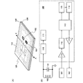
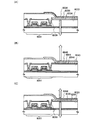
図1を用いて、本発明のIDチップの構成について説明する。図1(A)に、本発明のIDチップの一形態を斜視図で示す。100は集積回路、101は受光素子、102は発光素子、103はアンテナに相当する。受光素子101、発光素子102、アンテナ103は、共に集積回路100に電気的に接続されている。集積回路100、受光素子101、発光素子102及びアンテナ103は、基板104上に形成されている。また基板104には、集積回路100、受光素子101、発光素子102及びアンテナ103を間に挟んで、カバー材105が重なっている。
The configuration of the ID chip of the present invention will be described with reference to FIG. FIG. 1A is a perspective view showing an embodiment of the ID chip of the present invention.
なお図1(A)では、アンテナ103が、集積回路100と共に基板104とカバー材105の間に挟まれている構成を示しているが、本発明はこの構成に限定されない。例えば、カバー材105の基板104とは反対側にアンテナ103を形成しておき、カバー材105に開口部を形成し、該開口部を介して集積回路100とアンテナ103とを電気的に接続するようにしても良い。
Note that FIG. 1A illustrates a structure in which the
なお本発明のIDチップは、必ずしもアンテナ103を有している必要はない。アンテナ103を有さない場合、IDチップに、アンテナ103との電気的な接続を行なうための接続端子を設けるようにする。
Note that the ID chip of the present invention does not necessarily have the
また図1(A)では、カバー材105を用いてIDチップの機械的強度を高めている例を示しているが、本発明のIDチップは必ずしもカバー材105を用いている必要はない。例えば、集積回路100、受光素子101、発光素子102及びアンテナ103を樹脂等で覆うことで、IDチップの機械的強度を高めるようにしても良い。
1A shows an example in which the mechanical strength of the ID chip is increased using the
図1(B)に、図1(A)に示した本発明のIDチップの、機能的な構成をブロック図で示す。 FIG. 1B is a block diagram showing a functional configuration of the ID chip of the present invention shown in FIG.
集積回路100は、アンテナ103において生じる交流の電圧を、整流化するための整流回路110と、整流化された電圧から直流の電源電圧を生成するための電源回路111とを有する。なお図1(B)において118は、アンテナ103の両端子間に接続されている容量に相当する。電源回路111において生成された電源電圧は、集積回路100内の各種回路に供給される。
The
また集積回路100は、受光素子101から送られてきた電気信号を復調するための復調回路112と、復調回路112において復調された電気信号を用いて、各種演算処理を行なう論理回路113と、プログラムを含む各種データが格納されているメモリ114と、該論理回路113からの信号に従ってメモリ114の番地を指定し、データの書き込みまたは読み出しを行なうためのメモリコントロール回路115とを有する。また論理回路113では、各種演算処理またはメモリ114に格納されているデータを用いることにより、リーダ/ライタに送信するための電気信号を生成することができる。論理回路113において生成された電気信号は、発光素子102において光信号に変換されて、リーダ/ライタに送信される。
Further, the
なお、図1(B)では、1つの論理回路113を有する集積回路100を例示しているが、本発明はこの構成に限定されない。論理回路113において行なわれる演算処理の内容に合わせて、論理回路113を複数設けるようにしても良い。また、受光素子101において光信号から変換された電気信号を、復調回路112において復調する前に、アンプ116を用いて増幅するようにしても良い。また、論理回路113において生成された電気信号を、発光素子102に送信する前に、アンプ117を用いて増幅するようにしても良い。
Note that FIG. 1B illustrates the
またメモリ114は1つに限定されず、複数であっても良く、DRAM、SRAM、フラッシュメモリ、ROMまたはFRAM(登録商標)など、各種半導体メモリを用いることができる。メモリ114は、演算処理時の作業エリアとしても用いることができる。
The number of
また図1(B)は、交流の電圧を生成することができる発振回路と、論理回路113で生成された電気信号に従って、発振回路において生成された交流の電圧に変調を加える変調回路とを有していても良い。この場合発光素子102は、変調が加えられた交流の電圧を、光信号に変換し、リーダ/ライタに送信することができる。
FIG. 1B also includes an oscillation circuit that can generate an alternating voltage and a modulation circuit that modulates the alternating voltage generated in the oscillation circuit in accordance with the electrical signal generated by the
なお電源電圧を供給するための、電波の伝送方式は、図1(A)、図1(B)に示したような電磁結合方式に限定されず、電磁誘導方式、マイクロ波方式、その他の伝送方式を用いていても良い。 Note that the radio wave transmission method for supplying the power supply voltage is not limited to the electromagnetic coupling method as shown in FIGS. 1A and 1B, but an electromagnetic induction method, a microwave method, and other transmissions. A method may be used.
集積回路100は、絶縁分離されたTFTが用いられている。なお集積回路100に用いられる半導体素子はTFTに限定されず、あらゆる半導体素子を用いることができる。例えば、TFTの他に、記憶素子、ダイオード、光電変換素子、抵抗素子、コイル、容量素子、インダクタなどが代表的に挙げられる。
The
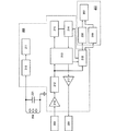
次に、本発明のICカードの構成について、図2及び図3を用いて説明する。図2(A)に、本発明のICカードの外観図を示す。201はカード本体であり、202はカード本体201に搭載されている表示装置207の画素部、203は受光素子、204は発光素子に相当する。
Next, the configuration of the IC card of the present invention will be described with reference to FIGS. FIG. 2A is an external view of the IC card of the present invention.
図2(B)に、図2(A)に示したカード本体201に含まれる、基板205の構成を示す。基板205には、薄膜の半導体膜で形成された集積回路206と、受光素子203と、発光素子204と、表示装置207と、アンテナ208が形成されている。
FIG. 2B illustrates a configuration of the
なお図2(B)では、集積回路206、受光素子203及び発光素子204と共に、アンテナ208を形成している例を示しているが、本発明のICカードはこの構成に限定されない。集積回路206とは別に形成しておいたアンテナを、集積回路206に電気的に接続しても良い。この場合、例えば銅線などをコイル状に巻き、100μm程度の厚さを有する2枚のプラスチックフィルムの間に該銅線を挟んでプレスしたものを、アンテナとして用いることができる。
Note that FIG. 2B illustrates an example in which the
また図2(B)では、1つのICカードにアンテナ208が1つだけ用いられているが、アンテナ208が複数用いられていても良い。
In FIG. 2B, only one
なお、図2(A)、図2(B)では、表示装置207を有するICカードの構成を示しているが、本発明はこの構成に限定されず、必ずしも表示装置を設ける必要はない。ただし、表示装置を設けることで、顔写真のデータを表示装置において表示させることができ、印刷法を用いた場合に比べて顔写真のすり替えを困難にすることができる。また顔写真以外の情報を表示することができ、ICカードの高機能化を実現することができる。
Note that FIGS. 2A and 2B illustrate the structure of an IC card having the
図3に、図2(B)に示した本発明のICカードの、機能的な構成をブロック図で示す。 FIG. 3 is a block diagram showing a functional configuration of the IC card of the present invention shown in FIG.
集積回路206は、図1(B)に示したIDチップの場合と同様に、整流回路210と、電源回路211とを有する。また221は、アンテナ208の両端子間に接続されている容量に相当する。また集積回路206は、復調回路212と、論理回路213と、メモリ214と、メモリコントロール回路215とを有する。さらに集積回路206は、復調回路212において復調される前の電気信号を増幅するためのアンプ216、発光素子204に送信する前の電気信号を増幅するためのアンプ217を有していても良い。これら集積回路206に含まれる各種回路の詳しい構成及び動作については、図1(B)についての説明を参照することができる。
The
さらに図2(B)に示した本発明のICカードの場合、集積回路206が、表示装置207に送る各種信号を生成するための、コントロール回路218を有している。コントロール回路218において生成した信号は、表示装置207が有する信号線駆動回路219及び走査線駆動回路220に送られる。そして信号線駆動回路219及び走査線駆動回路220によって画素部202の動作が制御されることで、画素部202に画像を表示することができる。
Further, in the case of the IC card of the present invention shown in FIG. 2B, the
なお図3に示すICカードは、交流の電圧を生成することができる発振回路と、論理回路213で生成された電気信号に従って、発振回路において生成された交流の電圧に変調を加える変調回路とを有していても良い。この場合発光素子204は、変調が加えられた交流の電圧を、光信号に変換し、リーダ/ライタに送信することができる。
The IC card shown in FIG. 3 includes an oscillation circuit that can generate an alternating voltage, and a modulation circuit that modulates the alternating voltage generated in the oscillation circuit in accordance with the electrical signal generated by the
なお電源電圧を供給するための、電波の伝送方式は、図2(B)、図3に示したような電磁結合方式に限定されず、電磁誘導方式、マイクロ波方式、その他の伝送方式を用いていても良い。 Note that the radio wave transmission method for supplying the power supply voltage is not limited to the electromagnetic coupling method as shown in FIGS. 2B and 3, and an electromagnetic induction method, a microwave method, and other transmission methods are used. May be.
集積回路206は、絶縁分離されたTFTが用いられている。なお集積回路206に用いられる半導体素子はTFTに限定されず、あらゆる半導体素子を用いることができる。例えば、TFTの他に、記憶素子、ダイオード、光電変換素子、抵抗素子、コイル、容量素子、インダクタなどが代表的に挙げられる。
The
なお、図1、図2及び図3に示すIDチップまたはICカードは、電源電圧の供給を、電波により行なっているが、本発明はこの構成に限定されない。アンテナの代わりに電池を用いて、集積回路への電源電圧の供給を行なっていても良い。図4(A)に、集積回路のうち、電源電圧の生成に関わっている部分のみを、ブロック図で示す。図4(A)において、301は電池に相当し、302は電源回路に相当する。電源回路は、電池301から供給される電源電圧を用い、各種回路に必要な高さの電源電圧を生成することができる。なお電池301として、化学電池、光電池などを用いることができる。
The ID chip or IC card shown in FIGS. 1, 2 and 3 supplies power supply voltage by radio waves, but the present invention is not limited to this configuration. A power supply voltage may be supplied to the integrated circuit using a battery instead of the antenna. FIG. 4A is a block diagram showing only a portion of the integrated circuit that is involved in generating a power supply voltage. In FIG. 4A, 301 corresponds to a battery, and 302 corresponds to a power supply circuit. The power supply circuit can generate a power supply voltage having a height required for various circuits using the power supply voltage supplied from the
図4(B)に、光電池の一種である太陽電池303を用いた、ICカードの外観図を示す。太陽電池303を用いることで、電池の交換及び電池への充電などを行なわなくとも、ICカードを用いることができる。また、アンテナに加えて、電源電圧の補助を行なうための電池を、IDチップまたはICカードに用いるようにしても良い。
FIG. 4B is an external view of an IC card using a
次に、本発明のIDチップの詳しい作製方法について説明する。なお本実施の形態では、絶縁分離されたTFTと、受光素子として用いるフォトダイオードとを、半導体素子の一例として示すが、集積回路に用いられる半導体素子はこれに限定されず、あらゆる回路素子を用いることができる。 Next, a detailed manufacturing method of the ID chip of the present invention will be described. Note that in this embodiment mode, an isolated TFT and a photodiode used as a light receiving element are shown as an example of a semiconductor element; however, a semiconductor element used in an integrated circuit is not limited to this, and any circuit element is used. be able to.
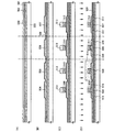
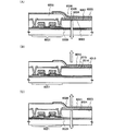
まず図5(A)に示すように、スパッタ法を用いて耐熱性を有する基板(第1の基板)500上に剥離層501を形成する。第1の基板500として、例えばバリウムホウケイ酸ガラスや、アルミノホウケイ酸ガラスなどのガラス基板、石英基板、セラミック基板等を用いることができる。また、ステンレス(SUS)基板を含む金属基板または半導体基板の表面に絶縁膜を形成したものを用いても良い。プラスチック等の可撓性を有する合成樹脂からなる基板は、一般的に上記基板と比較して耐熱温度が低い傾向にあるが、作製工程における処理温度に耐え得るのであれば用いることが可能である。
First, as illustrated in FIG. 5A, a
剥離層501は、非晶質シリコン、多結晶シリコン、単結晶シリコン、微結晶シリコン(セミアモルファスシリコンを含む)等、シリコンを主成分とする層を用いることができる。剥離層501は、スパッタ法、減圧CVD法、プラズマCVD法等を用いて形成することができる。本実施の形態では、膜厚50nm程度の非晶質シリコンを減圧CVD法で形成し、剥離層501として用いる。なお剥離層501はシリコンに限定されず、エッチングにより選択的に除去できる材料で形成すれば良い。剥離層501の膜厚は、50〜60nmとするのが望ましい。セミアモルファスシリコンに関しては、30〜50nmとしてもよい。
As the
次に、剥離層501上に、下地膜502を形成する。下地膜502は第1の基板500中に含まれるNaなどのアルカリ金属やアルカリ土類金属が、半導体膜中に拡散し、TFTなどの半導体素子の特性に悪影響を及ぼすのを防ぐために設ける。また下地膜502は、後の半導体素子を剥離する工程において、半導体素子を保護する役目も有している。下地膜502は単層であっても複数の絶縁膜を積層したものであっても良い。よってアルカリ金属やアルカリ土類金属の半導体膜への拡散を抑えることができる酸化珪素や、窒化珪素、窒化酸化珪素などの絶縁膜を用いて形成する。
Next, a
本実施の形態では、膜厚100nmのSiON膜、膜厚50nmのSiNO膜、膜厚100nmのSiON膜を順に積層して下地膜502を形成するが、各膜の材質、膜厚、積層数は、これに限定されるものではない。例えば、下層のSiON膜に代えて、膜厚0.5〜3μmのシロキサン系樹脂をスピンコート法、スリットコーター法、液滴吐出法、印刷法などによって形成しても良い。また、中層のSiNO膜に代えて、窒化珪素膜(SiNx、Si3N4等)を用いてもよい。また、上層のSiON膜に代えて、SiO2膜を用いていても良い。また、それぞれの膜厚は、0.05〜3μmとするのが望ましく、その範囲から自由に選択することができる。
In this embodiment mode, a
或いは、剥離層501に最も近い、下地膜502の下層をSiON膜またはSiO2膜で形成し、中層をシロキサン系樹脂で形成し、上層をSiO2膜で形成しても良い。
Alternatively, the lower layer of the
なお液滴吐出法とは、所定の組成物を含む液滴を細孔から吐出して所定のパターンを形成する方法を意味し、インクジェット法などがその範疇に含まれる。また印刷法にはスクリーン印刷法、オフセット印刷法などが含まれる。 The droplet discharge method means a method of forming a predetermined pattern by discharging droplets containing a predetermined composition from the pores, and includes an ink jet method and the like in its category. The printing method includes a screen printing method and an offset printing method.
ここで、酸化珪素膜は、SiH4/O2、TEOS(テトラエトキシシラン)/O2等の混合ガスを用い、熱CVD、プラズマCVD、常圧CVD、バイアスECRCVD等の方法によって形成することができる。また、窒化珪素膜は、代表的には、SiH4/NH3の混合ガスを用い、プラズマCVDによって形成することができる。また、酸化窒化珪素膜(SiOxNy:x>y)、窒化酸化珪素膜(SiNxOy:x>y)は、代表的には、SiH4/N2Oの混合ガスを用い、プラズマCVDによって形成することができる。 Here, the silicon oxide film may be formed by a method such as thermal CVD, plasma CVD, atmospheric pressure CVD, or bias ECRCVD using a mixed gas such as SiH 4 / O 2 , TEOS (tetraethoxysilane) / O 2, or the like. it can. The silicon nitride film can be typically formed by plasma CVD using a mixed gas of SiH 4 / NH 3 . The silicon oxynitride film (SiOxNy: x> y) and the silicon nitride oxide film (SiNxOy: x> y) are typically formed by plasma CVD using a mixed gas of SiH 4 / N 2 O. Can do.
次に、下地膜502上に半導体膜503を形成する。半導体膜503は、下地膜502を形成した後、大気に曝さずに形成することが望ましい。半導体膜503の膜厚は20〜200nm(望ましくは40〜170nm、好ましくは50〜150nm)とする。なお半導体膜503は、非晶質半導体であっても良いし、セミアモルファス半導体であっても良いし、多結晶半導体であっても良い。また半導体膜は珪素だけではなくシリコンゲルマニウムも用いることができる。シリコンゲルマニウムを用いる場合、ゲルマニウムの濃度は0.01〜4.5atomic%程度であることが好ましい。
Next, a
なお半導体膜503は、公知の技術により結晶化しても良い。公知の結晶化方法としては、レーザ光を用いたレーザ結晶化法、触媒元素を用いる結晶化法がある。或いは、触媒元素を用いる結晶化法とレーザ結晶化法とを組み合わせて用いることもできる。また、第1の基板500として石英のような耐熱性に優れている基板を用いる場合、電熱炉を使用した熱結晶化方法、赤外光を用いたランプアニール結晶化法、触媒元素を用いる結晶化法と、950℃程度の高温アニールを組み合わせた結晶法を用いても良い。
Note that the
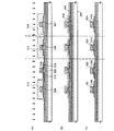
例えばレーザ結晶化を用いる場合、レーザ結晶化の前に、レーザに対する半導体膜503の耐性を高めるために、500℃、1時間の熱アニールを該半導体膜503に対して行なう。そして連続発振が可能な固体レーザを用い、基本波の第2高調波〜第4高調波のレーザ光を照射することで、大粒径の結晶を得ることができる。例えば、代表的には、Nd:YVO4レーザ(基本波1064nm)の第2高調波(532nm)や第3高調波(355nm)を用いるのが望ましい。具体的には、連続発振のYVO4レーザから射出されたレーザ光を非線形光学素子により高調波に変換し、出力10Wのレーザ光を得る。そして、好ましくは光学系により照射面にて矩形状または楕円形状のレーザ光に成形して、半導体膜503に照射する。このときのパワー密度は0.01〜100MW/cm2程度(好ましくは0.1〜10MW/cm2)が必要である。そして、走査速度を10〜2000cm/sec程度とし、照射する。
For example, when laser crystallization is used, thermal annealing is performed on the
また、パルス発振のレーザ光の発振周波数を10MHz以上とし、通常用いられている数十Hz〜数百Hzの周波数帯よりも著しく高い周波数帯を用いてレーザ結晶化を行なっても良い。パルス発振でレーザ光を半導体膜に照射してから半導体膜が完全に固化するまでの時間は数十nsec〜数百nsecと言われている。よって上記周波数を用いることで、半導体膜がレーザ光によって溶融してから固化するまでに、次のパルスのレーザ光を照射できる。したがって、半導体膜中において固液界面を連続的に移動させることができるので、走査方向に向かって連続的に成長した結晶粒を有する半導体膜が形成される。具体的には、含まれる結晶粒の走査方向における幅が10〜30μm、走査方向に対して垂直な方向における幅が1〜5μm程度の結晶粒の集合を形成することができる。該走査方向に沿って長く延びた単結晶の結晶粒を形成することで、少なくともTFTのチャネル方向には結晶粒界のほとんど存在しない半導体膜の形成が可能となる。 Alternatively, laser crystallization may be performed using a frequency band that is significantly higher than a frequency band of several tens to several hundreds Hz that is normally used, with an oscillation frequency of pulsed laser light of 10 MHz or higher. It is said that the time from irradiating a semiconductor film with laser light by pulse oscillation until the semiconductor film is completely solidified is several tens to several hundreds nsec. Therefore, by using the above frequency, the laser light of the next pulse can be irradiated from the time when the semiconductor film is melted by the laser light to solidify. Accordingly, since the solid-liquid interface can be continuously moved in the semiconductor film, a semiconductor film having crystal grains continuously grown in the scanning direction is formed. Specifically, a set of crystal grains having a width of 10 to 30 μm in the scanning direction of the included crystal grains and a width of about 1 to 5 μm in a direction perpendicular to the scanning direction can be formed. By forming single crystal grains extending long along the scanning direction, it is possible to form a semiconductor film having almost no crystal grain boundaries in at least the channel direction of the TFT.
なおレーザ結晶化は、連続発振の基本波のレーザ光と連続発振の高調波のレーザ光とを並行して照射するようにしても良いし、連続発振の基本波のレーザ光とパルス発振の高調波のレーザ光とを並行して照射するようにしても良い。 Laser crystallization may be performed by irradiating a continuous-wave fundamental laser beam and a continuous-wave harmonic laser beam in parallel, or a continuous-wave fundamental laser beam and a pulse oscillation harmonic. You may make it irradiate with the laser beam of a wave in parallel.
なお、希ガスや窒素などの不活性ガス雰囲気中でレーザ光を照射するようにしても良い。 Note that laser light may be irradiated in an inert gas atmosphere such as a rare gas or nitrogen.
上述したレーザ光の照射により、結晶性がより高められた半導体膜503が形成される。なお、予め多結晶半導体を、スパッタ法、プラズマCVD法、熱CVD法などで形成するようにしても良い。
By the above-described laser light irradiation, the
また本実施の形態では半導体膜503を結晶化しているが、結晶化せずに非晶質珪素膜または微結晶半導体膜のまま、後述のプロセスに進んでも良い。非晶質半導体、微結晶半導体を用いたTFTは、多結晶半導体を用いたTFTよりも作製工程が少ない分、コストを抑え、歩留まりを高くすることができるというメリットを有している。
In this embodiment mode, the
非晶質半導体は、珪化物気体をグロー放電分解することにより得ることができる。代表的な珪化物気体としては、SiH4、Si2H6が挙げられる。この珪化物気体を、水素、水素とヘリウムで希釈して用いても良い。 An amorphous semiconductor can be obtained by glow discharge decomposition of a silicide gas. Typical silicide gases include SiH 4 and Si 2 H 6 . This silicide gas may be diluted with hydrogen, hydrogen and helium.
なおセミアモルファス半導体とは、非晶質半導体と結晶構造を有する半導体(単結晶、多結晶を含む)の中間的な構造の半導体を含む膜である。このセミアモルファス半導体は、自由エネルギー的に安定な第3の状態を有する半導体であって、短距離秩序を持ち格子歪みを有する結晶質なものであり、その粒径を0.5〜20nmとして非単結晶半導体中に分散させて存在せしめることが可能である。セミアモルファス半導体は、そのラマンスペクトルが520cm-1よりも低波数側にシフトしており、またX線回折ではSi結晶格子に由来するとされる(111)、(220)の回折ピークが観測される。また、未結合手(ダングリングボンド)の中和剤として水素またはハロゲンを少なくとも1原子%またはそれ以上含ませている。ここでは便宜上、このような半導体をセミアモルファス半導体(SAS)と呼ぶ。さらに、ヘリウム、アルゴン、クリプトン、ネオンなどの希ガス元素を含ませて格子歪みをさらに助長させることで安定性が増し良好なセミアモルファス半導体が得られる。 Note that a semi-amorphous semiconductor is a film including a semiconductor having an intermediate structure between an amorphous semiconductor and a semiconductor having a crystal structure (including single crystal and polycrystal). This semi-amorphous semiconductor is a semiconductor having a third state which is stable in terms of free energy, and is a crystalline one having a short-range order and having a lattice strain, and having a grain size of 0.5 to 20 nm. It can be dispersed in a single crystal semiconductor. The semi-amorphous semiconductor has its Raman spectrum shifted to a lower wavenumber than 520 cm −1 , and diffraction peaks of (111) and (220), which are considered to be derived from the Si crystal lattice in X-ray diffraction, are observed. . Further, hydrogen or halogen is contained at least 1 atomic% or more as a neutralizing agent for dangling bonds. Here, for convenience, such a semiconductor is referred to as a semi-amorphous semiconductor (SAS). Further, by adding a rare gas element such as helium, argon, krypton, or neon to further promote lattice distortion, stability is improved and a good semi-amorphous semiconductor can be obtained.
またSASは珪化物気体をグロー放電分解することにより得ることができる。代表的な珪化物気体としては、SiH4であり、その他にもSi2H6、SiH2Cl2、SiHCl3、SiCl4、SiF4などを用いることができる。また水素や、水素にヘリウム、アルゴン、クリプトン、ネオンから選ばれた一種または複数種の希ガス元素を加えたガスで、この珪化物気体を希釈して用いることで、SASの形成を容易なものとすることができる。希釈率は2倍〜1000倍の範囲で珪化物気体を希釈することが好ましい。またさらに、珪化物気体中に、CH4、C2H6などの炭化物気体、GeH4、GeF4などのゲルマニウム化気体、F2などを混入させて、エネルギーバンド幅を1.5〜2.4eV、若しくは0.9〜1.1eVに調節しても良い。 SAS can be obtained by glow discharge decomposition of silicide gas. A typical silicide gas is SiH 4 , and in addition, Si 2 H 6 , SiH 2 Cl 2 , SiHCl 3 , SiCl 4 , SiF 4 and the like can be used. In addition, it is easy to form a SAS by diluting and using this silicide gas with hydrogen or a gas obtained by adding one or more kinds of rare gas elements selected from helium, argon, krypton, and neon to hydrogen. It can be. It is preferable to dilute the silicide gas at a dilution rate in the range of 2 to 1000 times. Furthermore, a carbide gas such as CH 4 or C 2 H 6 , a germanium gas such as GeH 4 or GeF 4 , F 2 or the like is mixed in the silicide gas, so that the energy bandwidth is 1.5-2. You may adjust to 4 eV or 0.9-1.1 eV.
例えば、SiH4にH2を添加したガスを用いる場合、或いはSiH4にF2を添加したガスを用いる場合、形成したセミアモルファス半導体を用いてTFTを作製すると、該TFTのサブスレッショルド係数(S値)を0.35V/sec以下、代表的には0.25〜0.09V/secとし、移動度を10cm2/Vsecとすることができる。そして上記セミアモルファス半導体を用いたTFTで、例えば19段リングオシレータを形成した場合、電源電圧3〜5Vにおいて、その発振周波数は1MH以上、好ましくは100MHz以上の特性を得ることができる。また電源電圧3〜5Vにおいて、インバータ1段あたりの遅延時間は26ns、好ましくは0.26ns以下とすることができる。 For example, when using a gas added with H 2 to SiH 4, or the case of using the added gas F 2 to SiH 4, when TFT is formed by using the formed semi-amorphous semiconductor, the subthreshold coefficient of the TFT (S Value) can be 0.35 V / sec or less, typically 0.25 to 0.09 V / sec, and the mobility can be 10 cm 2 / Vsec. When a TFT using the semi-amorphous semiconductor, for example, a 19-stage ring oscillator is formed, the oscillation frequency can be 1 MHz or more, preferably 100 MHz or more at a power supply voltage of 3 to 5V. In addition, at a power supply voltage of 3 to 5 V, the delay time per inverter stage can be 26 ns, preferably 0.26 ns or less.
次に、図5(B)に示すように、半導体膜503をパターニングし、島状の半導体膜504〜507を形成する。そして、島状の半導体膜504〜507を覆うように、ゲート絶縁膜508を形成する。ゲート絶縁膜508は、プラズマCVD法又はスパッタリング法などを用い、窒化珪素、酸化珪素、窒化酸化珪素又は酸化窒化珪素を含む膜を、単層で、又は積層させて形成することができる。積層する場合には、例えば、基板側から酸化珪素膜、窒化珪素膜、酸化珪素膜の3層構造とするのが好ましい。
Next, as illustrated in FIG. 5B, the
なお、ゲート絶縁膜508を形成した後、3〜100%の水素を含む雰囲気中で、300〜450℃で1〜12時間の熱処理を行ない、島状の半導体膜504〜507を水素化する工程を行なっても良い。また、水素化の他の手段として、プラズマ水素化(プラズマにより励起された水素を用いる)を行っても良い。この水素化の工程により、熱的に励起された水素によりダングリングボンドを終端することができる。また、後の工程において可撓性を有する第2の基板545上に半導体素子を貼り合わせた後、第2の基板545を曲げることにより半導体膜中に欠陥が形成されたとしても、水素化により半導体膜中の水素の濃度を、1×10¹⁹〜1×10²²atoms/cm3好ましくは1×1019〜5×1020atoms/cm3とすることで、半導体膜に含まれている水素によって該欠陥を終端させることができる。また該欠陥を終端させるために、半導体膜中にハロゲンを含ませておいても良い。
Note that after the
次に図5(C)に示すように、ゲート電極509〜512を形成する。本実施の形態では、SiとWをスパッタ法で積層するように形成した後、レジスト513をマスクとしてエッチングを行なうことにより、ゲート電極509〜512を形成した。勿論、ゲート電極509〜512の材料、構造、作製方法は、これに限定されるものではなく、適宜選択することができる。例えば、n型を付与する不純物がドーピングされたSiとNiSi(ニッケルシリサイド)との積層構造や、TaN(窒化タンタル)とW(タングステン)の積層構造としてもよい。また、種々の導電材料を用いて単層で形成しても良い。
Next, as shown in FIG. 5C,
また、レジストマスクの代わりに、SiOx等のマスクを用いてもよい。この場合、パターニングしてSiOx、SiON等のマスク(ハードマスクと呼ばれる。)を形成する工程が加わるが、エッチング時におけるマスクの膜減りがレジストよりも少ないため、所望の幅のゲート電極509〜512を形成することができる。また、レジスト513を用いずに、液滴吐出法を用いて選択的にゲート電極509〜512を形成しても良い。
In place of the resist mask, a mask such as SiOx may be used. In this case, a step of patterning to form a mask (referred to as a hard mask) of SiOx, SiON or the like is added, but since the mask film thickness during etching is less than that of the resist,
導電材料としては、導電膜の機能に応じて種々の材料を選択することができる。また、ゲート電極とアンテナとを同時に形成する場合には、それらの機能を考慮して材料を選択すればよい。 As the conductive material, various materials can be selected depending on the function of the conductive film. In the case where the gate electrode and the antenna are formed at the same time, materials may be selected in consideration of their functions.
なお、ゲート電極をエッチング形成する際のエッチングガスとしては、CF4、Cl2、O2の混合ガスやCl2ガスを用いたが、これに限定されるものではない。 Note that although a mixed gas of CF 4 , Cl 2 , and O 2 or Cl 2 gas is used as an etching gas for forming the gate electrode by etching, it is not limited to this.
次に図5(D)に示すように、pチャネル型TFTとなる島状の半導体膜505をレジスト514で覆い、ゲート電極509、511、512をマスクとして、島状の半導体膜504、506、507に、n型を付与する不純物元素(代表的にはP(リン)又はAs(砒素))を低濃度にドープする(第1のドーピング工程)。第1のドーピング工程の条件は、ドーズ量:1×10¹³〜6×10¹³/cm2、加速電圧:50〜70keVとしたが、これに限定されるものではない。この第1のドーピング工程によって、ゲート絶縁膜508を介してドーピングがなされ、島状の半導体膜504、506、507に、一対の低濃度不純物領域515〜517が形成される。なお、第1のドーピング工程は、pチャネル型TFTとなる島状の半導体膜505をレジストで覆わずに行っても良い。
Next, as illustrated in FIG. 5D, the island-shaped
次に図6(A)に示すように、レジスト514をアッシング等により除去した後、nチャネル型TFTとなる島状の半導体膜504、506、507を覆うように、レジスト518を新たに形成し、ゲート電極510をマスクとして、島状の半導体膜505に、p型を付与する不純物元素(代表的にはB(ホウ素))を高濃度にドープする(第2のドーピング工程)。第2のドーピング工程の条件は、ドーズ量:1×10¹⁶〜3×10¹⁶/cm2、加速電圧:20〜40keVとして行なう。この第2のドーピング工程によって、ゲート絶縁膜508を介してドーピングがなされ、島状の半導体膜505に、一対のp型の高濃度不純物領域519が形成される。
Next, as shown in FIG. 6A, after removing the resist 514 by ashing or the like, a resist 518 is newly formed so as to cover the island-shaped
次に図6(B)に示すように、レジスト518をアッシング等により除去した後、ゲート絶縁膜508及びゲート電極509〜512を覆うように、絶縁膜520を形成する。本実施の形態では、膜厚100nmのSiO2膜をプラズマCVD法によって形成した。その後、エッチバック法により、絶縁膜520、ゲート絶縁膜508を部分的にエッチングし、図6(C)に示すように、ゲート電極509〜512の側壁に接するように、サイドウォール521〜524を自己整合的(セルフアライン)に形成する。エッチングガスとしては、CHF3とHeの混合ガスを用いた。なお、サイドウォールを形成する工程は、これらに限定されるものではない。
Next, as shown in FIG. 6B, after the resist 518 is removed by ashing or the like, an insulating
なお、絶縁膜520を形成した時に、第1の基板500の裏面にも絶縁膜が形成された場合には、レジストを用い、裏面に形成された絶縁膜を選択的にエッチングし、除去するようにしても良い。この場合、裏面に形成された絶縁膜は、サイドウォール521〜524をエッチバック法で形成する際に、絶縁膜520、ゲート絶縁膜508と共にエッチングして、除去するようにしても良い。
When the insulating film is formed on the back surface of the
次に図7(A)に示すように、pチャネル型TFTとなる島状の半導体膜505を覆うように、レジスト525を新たに形成し、ゲート電極509、511、512及びサイドウォール521、523、524をマスクとして、n型を付与する不純物元素(代表的にはP又はAs)を高濃度にドープする(第3のドーピング工程)。第3のドーピング工程の条件は、ドーズ量:1×10¹³〜5×10¹⁵/cm2、加速電圧:60〜100keVとして行なう。この第3のドーピング工程によって、島状の半導体膜504、506、507に、一対のn型の高濃度不純物領域526〜528が形成される。
Next, as shown in FIG. 7A, a resist 525 is newly formed so as to cover the island-shaped
なおサイドウォール521、523、524は、後に高濃度のn型を付与する不純物をドーピングし、サイドウォール521、523、524の下部に低濃度不純物領域又はノンドープのオフセット領域を形成する際のマスクとして機能するものである。よって、低濃度不純物領域又はオフセット領域の幅を制御するには、絶縁膜520の厚さやサイドウォール521、523、524を形成する際のエッチバック法の条件を適宜変更し、サイドウォール521、523、524のサイズを調整すればよい。
Note that the
次に、レジスト525をアッシング等により除去した後、不純物領域の熱活性化を行っても良い。例えば、50nmのSiON膜を成膜した後、550℃、4時間、窒素雰囲気下において、加熱処理を行なえばよい。また、水素を含むSiNx膜を、100nmの膜厚に形成した後、410℃、1時間、窒素雰囲気下において、加熱処理を行なうことにより、多結晶半導体膜の欠陥を改善することができる。これは、例えば、多結晶半導体膜中に存在するダングリングボンドを終端させるものであり、水素化処理工程などと呼ばれる。 Next, after removing the resist 525 by ashing or the like, the impurity regions may be thermally activated. For example, after a 50 nm SiON film is formed, heat treatment may be performed in a nitrogen atmosphere at 550 ° C. for 4 hours. In addition, after the SiNx film containing hydrogen is formed to a thickness of 100 nm, defects in the polycrystalline semiconductor film can be improved by performing heat treatment at 410 ° C. for 1 hour in a nitrogen atmosphere. This terminates dangling bonds existing in the polycrystalline semiconductor film, for example, and is called a hydrogenation process.
上述した一連の工程により、nチャネル型TFT529、pチャネル型TFT530、nチャネル型TFT531、nチャネル型TFT532が形成される。なお、nチャネル型TFT531は、フォトダイオードとして用いることができる。上記作製工程において、エッチバック法の条件を適宜変更し、サイドウォールのサイズを調整することで、チャネル長0.2μm〜2μmのTFTを形成することができる。なお、本実施の形態では、TFT529〜532をトップゲート構造としたが、ボトムゲート構造(逆スタガ構造)としてもよい。
Through the series of steps described above, an n-
さらに、この後、TFT529〜532を保護するためのパッシベーション膜を形成しても良い。パッシベーション膜は、アルカリ金属やアルカリ土類金属のTFT529〜532への侵入を防ぐことができる、窒化珪素、窒化酸化珪素、窒化アルミニウム、酸化アルミニウム、酸化珪素などを用いるのが望ましい。具体的には、例えば膜厚600nm程度のSiON膜を、パッシベーション膜として用いることができる。この場合、水素化処理工程は、該SiON膜形成後に行っても良い。このように、TFT529〜532上には、SiON、SiNx、SiONの3層の絶縁膜が形成されることになるが、その構造や材料はこれらに限定されるものではない。上記構成を用いることで、TFT529〜532が下地膜502とパッシベーション膜とで覆われるため、Naなどのアルカリ金属やアルカリ土類金属が、半導体素子に用いられている半導体膜中に拡散し、半導体素子の特性に悪影響を及ぼすのをより防ぐことができる。
Further, after that, a passivation film for protecting the
次に図7(B)に示すように、TFT529〜532を覆うように、第1の層間絶縁膜533を形成する。第1の層間絶縁膜533は、ポリイミド、アクリル、ポリアミド等の、耐熱性を有する有機樹脂を用いることができる。また上記有機樹脂の他に、低誘電率材料(low−k材料)、シロキサン系樹脂等を用いることができる。なお、シロキサン系樹脂とは、Si−O−Si結合を含む樹脂に相当する。シロキサンは、シリコン(Si)と酸素(O)との結合で骨格構造が構成される。置換基として、少なくとも水素を含む有機基(例えばアルキル基、芳香族炭化水素)が用いられる。置換基として、フルオロ基を用いてもよい。または置換基として、少なくとも水素を含む有機基と、フルオロ基とを用いてもよい。第1の層間絶縁膜533の形成には、その材料に応じて、スピンコート、ディップ、スプレー塗布、液滴吐出法(インクジェット法、スクリーン印刷、オフセット印刷等)、ドクターナイフ、ロールコーター、カーテンコーター、ナイフコーター等を採用することができる。また、無機材料を用いてもよく、その際には、酸化珪素、窒化珪素、酸窒化珪素、PSG(リンガラス)、BPSG(リンボロンガラス)、アルミナ膜等を用いることができる。なお、これらの絶縁膜を積層させて、第1の層間絶縁膜533を形成しても良い。
Next, as shown in FIG. 7B, a first
さらに本実施の形態では、第1の層間絶縁膜533上に、第2の層間絶縁膜534を形成する。第2の層間絶縁膜534としては、DLC(ダイヤモンドライクカーボン)或いは窒化炭素(CN)等の炭素を有する膜、又は、酸化珪素膜、窒化珪素膜或いは窒化酸化珪素膜等を用いることができる。形成方法としては、プラズマCVD法や、大気圧プラズマ等を用いることができる。あるいは、ポリイミド、アクリル、ポリアミド、レジスト又はベンゾシクロブテン等の感光性又は非感光性の有機材料や、シロキサン系樹脂等を用いてもよい。
Further, in this embodiment, a second
なお、第1の層間絶縁膜533又は第2の層間絶縁膜534と、後に形成される配線を構成する導電材料等との熱膨張率の差から生じる応力によって、第1の層間絶縁膜533又は第2の層間絶縁膜534の膜剥がれや割れが生じるのを防ぐために、第1の層間絶縁膜533又は第2の層間絶縁膜534中にフィラーを混入させておいても良い。
Note that the first
次に図7(B)に示すように、第1の層間絶縁膜533及び第2の層間絶縁膜534にコンタクトホールを形成し、TFT529〜532に接続する配線535〜541を形成する。コンタクトホール開孔時のエッチングに用いられるガスは、CHF3とHeの混合ガスを用いたが、これに限定されるものではない。本実施の形態では、配線535〜541を、Alで形成した。なお配線535〜541をTi、TiN、Al−Si、Ti、TiNの順で積層した5層構造とし、スパッタ法を用いて形成しても良い。
Next, as shown in FIG. 7B, contact holes are formed in the first
なお、Alにおいて、Siを混入させることにより、配線パターニング時のレジストベークにおけるヒロックの発生を防止することができる。また、Siの代わりに、0.5%程度のCuを混入させても良い。また、TiやTiNでAl−Si層をサンドイッチすることにより、耐ヒロック性がさらに向上する。なお、パターニング時には、SiON等からなる上記ハードマスクを用いるのが望ましい。なお、配線の材料や、形成方法はこれらに限定されるものではなく、前述したゲート電極に用いられる材料を採用しても良い。 In addition, by mixing Si in Al, generation of hillocks in resist baking at the time of wiring patterning can be prevented. Further, instead of Si, about 0.5% Cu may be mixed. Further, the hillock resistance is further improved by sandwiching the Al—Si layer with Ti or TiN. In the patterning, it is desirable to use the hard mask made of SiON or the like. Note that the wiring material and the formation method are not limited to these, and the material used for the gate electrode described above may be employed.
なお、配線535、536はnチャネル型TFT529の高濃度不純物領域526に、配線536、537はpチャネル型TFT530の高濃度不純物領域519に、配線538、539はnチャネル型TFT531の高濃度不純物領域527に、配線540、541はnチャネル型TFT532の高濃度不純物領域528に、それぞれ接続されている。
Note that the
次に図7(C)に示すように、配線535〜541を覆うように、第2の層間絶縁膜534上に保護層542を形成する。保護層542は、後に剥離層501をエッチングにより除去する際にTFT529〜532及び配線535〜541を保護することができる材料を用いる。例えば、水またはアルコール類に可溶なエポキシ系、アクリレート系、シリコン系の樹脂を全面に塗布することで保護層542を形成することができる。
Next, as illustrated in FIG. 7C, a
本実施の形態では、スピンコート法で水溶性樹脂(東亜合成製:VL−WSHL10)を膜厚30μmとなるように塗布し、仮硬化させるために2分間の露光を行ったあと、UV光を裏面から2.5分、表面から10分、合計12.5分の露光を行って本硬化させて、保護層542を形成する。なお、複数の有機樹脂を積層する場合、有機樹脂同士では使用している溶媒によって塗布または焼成時に一部溶解したり、密着性が高くなりすぎたりする恐れがある。従って、第2の層間絶縁膜534と保護層542を共に同じ溶媒に可溶な有機樹脂を用いる場合、後の工程において保護層542の除去がスムーズに行なわれるように、第2の層間絶縁膜534を覆うように、無機絶縁膜(SiNX膜、SiNXOY膜、AlNX膜、またはAlNXOY膜)を形成しておくことが好ましい。
In the present embodiment, a water-soluble resin (manufactured by Toagosei Co., Ltd .: VL-WSHL10) is applied by spin coating so as to have a film thickness of 30 μm, and after exposure for 2 minutes for temporary curing, UV light is applied. Exposure is performed for 2.5 minutes from the back surface and 10 minutes from the front surface for a total of 12.5 minutes, followed by main curing to form the
次に図8(A)に示すように、IDチップどうしを分離するために溝543を形成する。溝543は、剥離層501が露出する程度の深さを有していれば良い。溝543の形成は、ダイシング、スクライビングなどを用いることができる。なお、第1の基板500上に形成されているIDチップを分離する必要がない場合、必ずしも溝543を形成する必要はない。
Next, as shown in FIG. 8A, a
次に図8(B)に示すように、剥離層501をエッチングにより除去する。本実施の形態では、エッチングガスとしてフッ化ハロゲンを用い、該ガスを溝543から導入する。本実施の形態では、例えばClF3(三フッ化塩素)を用い、温度:350℃、流量:300sccm、気圧:799.8Pa(6Torr)、時間:3hの条件で行なう。また、ClF3ガスに窒素を混ぜたガスを用いても良い。ClF3等のフッ化ハロゲンを用いることで、剥離層501が選択的にエッチングされ、第1の基板500をTFT529〜532から剥離することができる。なおフッ化ハロゲンは、気体であっても液体であってもどちらでも良い。
Next, as shown in FIG. 8B, the
次に図9(A)に示すように、剥離されたTFT529〜532を、接着剤544を用いて第2の基板545に貼り合わせる。接着剤544は、第2の基板545と下地膜502とを貼り合わせることができる材料を用いる。接着剤544は、例えば反応硬化型接着剤、熱硬化型接着剤、紫外線硬化型接着剤等の光硬化型接着剤、嫌気型接着剤などの各種硬化型接着剤を用いることができる。
Next, as illustrated in FIG. 9A, the peeled
第2の基板545として、例えばバリウムホウケイ酸ガラスや、アルミノホウケイ酸ガラスなどのガラス基板、フレキシブルな紙またはプラスチックなどの有機材料を用いることができる。または第2の基板545として、フレキシブル無機材料を用いていても良い。プラスチック基板は、極性基のついたポリノルボルネンからなるARTON(JSR製)を用いることができる。また、ポリエチレンテレフタレート(PET)に代表されるポリエステル、ポリエーテルスルホン(PES)、ポリエチレンナフタレート(PEN)、ポリカーボネート(PC)、ナイロン、ポリエーテルエーテルケトン(PEEK)、ポリスルホン(PSF)、ポリエーテルイミド(PEI)、ポリアリレート(PAR)、ポリブチレンテレフタレート(PBT)、ポリイミド、アクリロニトリルブタジエンスチレン樹脂、ポリ塩化ビニル、ポリプロピレン、ポリ酢酸ビニル、アクリル樹脂などが挙げられる。第2の基板545は集積回路において発生した熱を拡散させるために、2〜30W/mK程度の高い熱伝導率を有する方が望ましい。
As the
次に図9(B)に示すように、配線535〜541を覆うように、第2の層間絶縁膜534上に隔壁546を形成する。隔壁546は、配線535の一部及び配線541の一部が露出するような、開口部を有する。また隔壁546は、有機樹脂膜、無機絶縁膜またはシロキサン系絶縁膜を用いて形成することができる。有機樹脂膜ならば、例えばアクリル、ポリイミド、ポリアミドなど、無機絶縁膜ならば酸化珪素、窒化酸化珪素などを用いることができる。特に感光性の有機樹脂膜を隔壁546に用い、配線541の露出している開口部の側壁が、連続した曲率を持って形成される傾斜面となるように形成することで、配線541と、後に形成される電極548とが接続してしまうのを防ぐことができる。このとき、マスクを液滴吐出法または印刷法で形成することができる。また隔壁546自体を、液滴吐出法または印刷法で形成することもできる。
Next, as illustrated in FIG. 9B, a
次に、発光素子549またはアンテナ550を形成する。本実施の形態では、発光素子549を先に形成する形態について説明するが、アンテナ550を先に形成しても良いし、発光素子549が有する電極548を形成する際にアンテナ550も共に形成するようにしても良い。
Next, the light-emitting
まず光電変換を行なうための層に相当する、電界発光層547を形成する前に、隔壁546及び配線541に吸着した水分や酸素等を除去するために、大気雰囲気下で加熱処理または真空雰囲気下で加熱処理(真空ベーク)を行なっても良い。具体的には、基板の温度を200℃〜450℃、好ましくは250〜300℃で、0.5〜20時間程度、真空雰囲気下で加熱処理を行なう。望ましくは3×10⁻⁷Torr以下とし、可能であるならば3×10⁻⁸Torr以下とするのが最も望ましい。そして、真空雰囲気下で加熱処理を行なった後に電界発光層547を形成する場合、電界発光層547を形成する直前まで当該基板を真空雰囲気下に置いておくことで、信頼性をより高めることができる。また陽極はたは陰極として用いる配線541は、真空ベークの前に、その表面が平坦化されるように、CMP法、ポリビニルアルコール系の多孔質体を用いて、研磨しておいても良い。またCMP法を用いた研磨後に、陽極または陰極として用いる配線541の表面に紫外線照射、酸素プラズマ処理などを行ってもよい。
First, before the
そして、隔壁546の開口部において配線541と接するように、電界発光層547を形成する。電界発光層547は、単数の層で構成されていても、複数の層が積層されるように構成されていてもどちらでも良い。本実施の形態では、配線541を陰極として用いるので、電界発光層547が複数の層で構成されている場合、配線541上に、電子注入層、電子輸送層、発光層、ホール輸送層、ホール注入層の順に積層する。なお配線541が陽極に相当する場合は、電界発光層547を、ホール注入層、ホール輸送層、発光層、電子輸送層、電子注入層の順に積層して形成する。
Then, an
なお、電界発光層547の積層構造及び各層に用いる電界発光材料を適宜変更することで、赤外光を発する発光素子549を形成することができる。
Note that the light-emitting
なお、カラーフィルターを設けて、特定の波長領域の光を透過させるようにしても良い。カラーフィルターは、特定の波長領域の光を透過させることができる着色層と、場合によっては該着色層に加え、可視光を遮蔽することができる遮蔽膜とを有する場合がある。そしてカラーフィルターは、発光素子を封止するためのカバー材上に形成する場合もあれば、基板に形成する場合もありうる。いずれの場合においても、着色層または遮蔽膜は、印刷法または液滴吐出法を用いて形成することが可能である。 A color filter may be provided to transmit light in a specific wavelength region. The color filter may have a colored layer that can transmit light in a specific wavelength region and a shielding film that can shield visible light in addition to the colored layer in some cases. The color filter may be formed on a cover material for sealing the light emitting element, or may be formed on a substrate. In any case, the colored layer or the shielding film can be formed using a printing method or a droplet discharge method.
そして電界発光層547を覆うように、電極548を形成する。配線541が陰極の場合、電極548は陽極に相当する。逆に、配線541が陽極の場合、電極548は陰極に相当する。電極548の作製方法は、蒸着法、スパッタ法、液滴吐出法などを材料に合わせて使い分けることが好ましい。
Then, an
また電界発光層547は、高分子系有機化合物、中分子系有機化合物、低分子系有機化合物、無機化合物のいずれを用いていても、液滴吐出法で形成することが可能である。また中分子系有機化合物、低分子系有機化合物、無機化合物は蒸着法で形成しても良い。ただし、後にアンテナ550が形成される領域とは異なる領域に、電界発光層547及び電極548を形成するようにする。
The
陽極には、酸化インジウムスズ(ITO)、酸化亜鉛(ZnO)、酸化インジウム亜鉛(IZO)、ガリウムを添加した酸化亜鉛(GZO)などその他の透光性酸化物導電材料を用いることが可能である。ITO及び酸化珪素を含む酸化インジウムスズ(以下、ITSOとする)や、酸化珪素を含んだ酸化インジウムに、さらに2〜20%の酸化亜鉛(ZnO)を混合したものを用いても良い。また陽極として上記透光性酸化物導電材料の他に、例えばTiN、ZrN、Ti、W、Ni、Pt、Cr、Ag、Al等の1つまたは複数からなる単層膜の他、窒化チタンとアルミニウムを主成分とする膜との積層、窒化チタン膜とアルミニウムを主成分とする膜と窒化チタン膜との三層構造等を用いることができる。ただし透光性酸化物導電材料以外の材料で陽極側から光を取り出す場合、光が透過する程度の膜厚(好ましくは、5nm〜30nm程度)で形成する。 For the anode, other light-transmitting oxide conductive materials such as indium tin oxide (ITO), zinc oxide (ZnO), indium zinc oxide (IZO), and gallium-added zinc oxide (GZO) can be used. . Indium tin oxide containing ITO and silicon oxide (hereinafter referred to as ITSO) or indium oxide containing silicon oxide mixed with 2 to 20% zinc oxide (ZnO) may be used. In addition to the light-transmitting oxide conductive material as an anode, in addition to a single layer film made of, for example, one or more of TiN, ZrN, Ti, W, Ni, Pt, Cr, Ag, Al, etc., titanium nitride and A stack of a film containing aluminum as its main component, a three-layer structure of a titanium nitride film, a film containing aluminum as its main component, and a titanium nitride film can be used. However, when light is extracted from the anode side with a material other than the light-transmitting oxide conductive material, the light-transmitting oxide film is formed to have a film thickness that allows light to pass (preferably about 5 nm to 30 nm).
陰極は、仕事関数の小さい金属、合金、電気伝導性化合物、およびこれらの混合物などを用いることができる。具体的には、LiやCs等のアルカリ金属、およびMg、Ca、Sr等のアルカリ土類金属、これらを含む合金(Mg:Ag、Al:Li、Mg:Inなど)、およびこれらの化合物(CaF2、CaN)の他、YbやEr等の希土類金属を用いることができる。また電子注入層を設ける場合、Alなどの他の導電層を用いることも可能である。また陰極側から光を取り出す場合は、酸化インジウムスズ(ITO)、酸化亜鉛(ZnO)、酸化インジウム亜鉛(IZO)、ガリウムを添加した酸化亜鉛(GZO)などその他の透光性酸化物導電材料を用いることが可能である。ITO及び酸化珪素を含む酸化インジウムスズ(以下、ITSOとする)や、酸化珪素を含んだ酸化インジウムに、さらに2〜20%の酸化亜鉛(ZnO)を混合したものを用いても良い。透光性酸化物導電材料を用いる場合、電界発光層547に電子注入層を設けるのが望ましい。また透光性酸化物導電材料を用いずとも、陰極を光が透過する程度の膜厚(好ましくは、5nm〜30nm程度)で形成することで、陰極側から光を取り出すことができる。この場合、該陰極の上または下に接するように透光性酸化物導電材料を用いて透光性を有する導電層を形成し、陰極のシート抵抗を抑えるようにしても良い。
As the cathode, a metal, an alloy, an electrically conductive compound, a mixture thereof, or the like having a low work function can be used. Specifically, alkali metals such as Li and Cs, and alkaline earth metals such as Mg, Ca, and Sr, alloys containing these (Mg: Ag, Al: Li, Mg: In, etc.), and compounds thereof ( In addition to CaF 2 and CaN, rare earth metals such as Yb and Er can be used. When an electron injection layer is provided, other conductive layers such as Al can be used. When light is extracted from the cathode side, other light-transmitting oxide conductive materials such as indium tin oxide (ITO), zinc oxide (ZnO), indium zinc oxide (IZO), and gallium-added zinc oxide (GZO) are used. It is possible to use. Indium tin oxide containing ITO and silicon oxide (hereinafter referred to as ITSO) or indium oxide containing silicon oxide mixed with 2 to 20% zinc oxide (ZnO) may be used. In the case of using a light-transmitting oxide conductive material, it is desirable to provide an electron injection layer in the
なお、第2の層間絶縁膜534を窒化珪素または窒化酸化珪素で形成し、第2の層間絶縁膜534と接する配線541を、ITSOなどの透光性酸化物導電材料と酸化珪素を含む導電膜で形成することで、上述した、配線541と第2の層間絶縁膜534の、どの材料の組み合わせよりも、発光素子549の輝度を高めることができる。なお、配線541にITSOを用いた場合、含まれる酸化珪素によって水分が付着しやすいので、上述した真空ベークは特に有効である。
Note that the second
隔壁546の開口部において、配線541と電界発光層547と電極548が重なり合うことで、発光素子549が形成される。
In the opening of the
なお、発光素子549からの光の取り出しは、配線541側からであっても良いし、電極548側からであっても良いし、その両方からであっても良い。上記3つの構成にうち、目的とする構成に合わせて、陽極、陰極ぞれぞれの材料及び膜厚を選択するようにする。
Note that light can be extracted from the light-emitting
次にアンテナ550の作製方法について説明する。アンテナ550は、導電膜をパターニングして発光素子549が有する電極548を形成する際に、同時に形成しておいても良いし、別個の作製方法を用いて形成しても良い。本実施の形態では、電極548とは別個の作製方法を用いて、アンテナ550を形成する例について説明する。
Next, a method for manufacturing the
図9(B)に、隔壁546上に形成されたアンテナ550の様子を示す。アンテナ550は、Ag、Au、Cu、Pd、Cr、Mo、Ti、Ta、W、Al、Fe、Co、Zn、Sn、Niなどの金属、金属化合物を1つまたは複数有する導電材料を用いることができる。そしてアンテナ550は、配線535と接続されている。なお図9(B)では、アンテナ550が配線535と直接接続されているが、本発明のIDチップはこの構成に限定されない。例えば別途形成した配線を用いて、アンテナ550と配線535とを電気的に接続するようにしても良い。
FIG. 9B shows a state of the
アンテナ550は印刷法、フォトリソグラフィ法、蒸着法または液滴吐出法などを用いて形成することができる。本実施の形態では、アンテナ550が単層の導電膜で形成されているが、複数の導電膜が積層されたアンテナ550を形成することも可能である。例えば、Niなどで形成した配線に、Cuを無電解めっきでコーティングして、アンテナ550を形成しても良い。
The
印刷法、液滴吐出法を用いることで、露光用のマスクを用いずとも、アンテナ550を形成することが可能になる。また、液滴吐出法、印刷法だと、フォトリソグラフィ法と異なり、エッチングにより除去されてしまうような材料の無駄がない。また高価な露光用のマスクを用いなくとも良いので、IDチップの作製に費やされるコストを抑えることができる。
By using a printing method or a droplet discharge method, the
液滴吐出法または各種印刷法を用いる場合、例えば、CuをAgでコートした導電粒子なども用いることが可能である。なお液滴吐出法を用いてアンテナ550を形成する場合、該アンテナ550の密着性が高まるような処理を、隔壁546の表面に施すことが望ましい。
In the case of using a droplet discharge method or various printing methods, for example, conductive particles in which Cu is coated with Ag can be used. Note that in the case where the
密着性を高めることができる方法として、具体的には、例えば触媒作用により導電膜または絶縁膜の密着性を高めることができる金属または金属化合物を隔壁546の表面に付着させる方法、形成される導電膜または絶縁膜との密着性が高い有機系の絶縁膜、金属、金属化合物を隔壁546の表面に付着させる方法、隔壁546の表面に大気圧下または減圧下においてプラズマ処理を施し、表面改質を行なう方法などが挙げられる。また、上記導電膜または絶縁膜との密着性が高い金属として、チタン、チタン酸化物の他、3d遷移元素であるSc、Ti、V、Cr、Mn、Fe、Co、Ni、Cu、Znなどが挙げられる。また金属化合物として、上述した金属の酸化物、窒化物、酸窒化物などが挙げられる。上記有機系の絶縁膜として、例えばポリイミド、シロキサン系樹脂等が挙げられる。
As a method for improving the adhesion, specifically, for example, a method of attaching a metal or a metal compound capable of improving the adhesion of the conductive film or the insulating film to the surface of the
隔壁546に付着させる金属または金属化合物が導電性を有する場合、アンテナの正常な動作が妨げられないように、そのシート抵抗を制御する。具体的には、導電性を有する金属または金属化合物の平均の厚さを、例えば1〜10nmとなるように制御したり、該金属または金属化合物を酸化により部分的に、または全体的に絶縁化したりすれば良い。或いは、密着性を高めたい領域以外は、付着した金属または金属化合物をエッチングにより選択的に除去しても良い。また金属または金属化合物を、予め基板の全面に付着させるのではなく、液滴吐出法、印刷法、ゾル−ゲル法などを用いて特定の領域にのみ選択的に付着させても良い。なお金属または金属化合物は、隔壁546の表面において完全に連続した膜状である必要はなく、ある程度分散した状態であっても良い。
When the metal or metal compound attached to the
なお、発光素子549、アンテナ550を形成したら、発光素子549またはアンテナ550を覆うように、保護膜を形成しても良い。保護膜は、水分や酸素などの発光素子の劣化を促進させる原因となる物質を、他の絶縁膜と比較して透過させにくい膜を用いる。代表的には、例えばDLC膜、窒化炭素膜、RFスパッタ法、CVD法などで形成された窒化珪素膜等を用いるのが望ましい。また、例えば窒化炭素膜と窒化珪素を積層した膜、ポリスチレンを積層した膜などを、保護膜として用いても良い。また上述した水分や酸素などの物質を透過させにくい膜と、該膜に比べて水分や酸素などの物質を透過させやすいが内部応力の低い膜とを積層させて、保護膜として用いることも可能である。本実施の形態では窒化珪素を用いる。保護膜として窒化珪素を用いる場合、低い成膜温度で緻密な保護膜を形成するには、アルゴンなどの希ガス元素を反応ガスに含ませ、保護膜中に混入させると良い。
Note that after the light-emitting
次に図9(C)に示すように、発光素子549及びアンテナ550を覆うように、接着剤551を隔壁546上に塗布し、カバー材552を貼り合わせる。カバー材552は第2の基板545と同様の材料を用いることができる。接着剤551の厚さは、例えば10〜200μmとすれば良い。
Next, as illustrated in FIG. 9C, an adhesive 551 is applied over the
また接着剤551は、カバー材552と隔壁546及びアンテナ550とを貼り合わせることができる材料を用いる。接着剤551は、例えば反応硬化型接着剤、熱硬化型接着剤、紫外線硬化型接着剤等の光硬化型接着剤、嫌気型接着剤などの各種硬化型接着剤を用いることができる。
For the adhesive 551, a material that can bond the
上述した各工程を経て、IDチップが完成する。上記作製方法によって、トータルの膜厚0.3μm以上3μm以下、代表的には2μm程度の飛躍的に薄い集積回路を第2の基板545とカバー材552との間に形成することができる。なお集積回路の厚さは、半導体素子自体の厚さのみならず、接着剤544と接着剤551間に形成された各種絶縁膜及び層間絶縁膜の厚さを含めるものとする。またIDチップが有する集積回路の占める面積を、5mm四方(25mm2)以下、より望ましくは0.3mm四方(0.09mm2)〜4mm四方(16mm2)程度とすることができる。
The ID chip is completed through the above-described steps. By the above manufacturing method, an extremely thin integrated circuit having a total film thickness of 0.3 μm to 3 μm, typically about 2 μm, can be formed between the
なお集積回路を、第2の基板545とカバー材552の間のより中央に位置させることで、IDチップの機械的強度を高めることができる。具体的には、第2の基板545とカバー材552の間の距離をdとすると、第2の基板545と、集積回路の厚さ方向における中心Oとの距離xが、以下の数1に示す式を満たすように、接着剤544、接着剤551の厚さを制御することが望ましい。
Note that the mechanical strength of the ID chip can be increased by positioning the integrated circuit more centrally between the
![]()
![]()
また好ましくは、以下の数2に示す式を満たすように、接着剤544、接着剤551の厚さを制御する。 In addition, preferably, the thicknesses of the adhesive 544 and the adhesive 551 are controlled so as to satisfy the following equation (2).
![]()
![]()
また、図10に示すように、集積回路におけるTFTの島状の半導体膜から下部の下地膜までの距離(tunder)と、島状の半導体膜から上部の隔壁546までの距離(tover)が、等しく又は概略等しくなるように、下地膜502、第1の層間絶縁膜533、第2の層間絶縁膜534または隔壁546の厚さを調整しても良い。このようにして、島状の半導体膜を集積回路の中央に配置せしめることで、半導体層への応力を緩和することができ、クラックの発生を防止することができる。
As shown in FIG. 10, the distance (t under ) from the island-shaped semiconductor film of the TFT in the integrated circuit to the lower base film, and the distance from the island-shaped semiconductor film to the upper partition 546 (t over ). However, the thicknesses of the
なお図9(C)では、カバー材552を用いる例を示しているが、本発明はこの構成に限定されない。例えば図9(B)に示した工程までで終了としても良いし、図9(B)に示した工程の後に、アンテナ550及び発光素子549を保護するための層を形成して、完成としても良い。
Note that FIG. 9C illustrates an example in which the
なお本実施の形態では、耐熱性の高い第1の基板500と集積回路の間に剥離層を設け、エッチングにより該剥離層を除去することで基板と集積回路とを剥離する方法について示したが、本発明のIDチップの作製方法は、この構成に限定されない。例えば、耐熱性の高い基板と集積回路の間に金属酸化膜を設け、該金属酸化膜を結晶化により脆弱化して集積回路を剥離しても良い。或いは、耐熱性の高い基板と集積回路の間に、水素を含む非晶質半導体膜を用いた剥離層を設け、レーザ光の照射により該剥離層を除去することで基板と集積回路とを剥離しても良い。或いは、集積回路が形成された耐熱性の高い基板を機械的に削除または溶液やガスによるエッチングで除去することで集積回路を基板から切り離しても良い。
Note that although this embodiment mode shows a method for separating a substrate and an integrated circuit by providing a separation layer between the
またIDチップの可撓性を確保するために、下地膜502に接する接着剤544に有機樹脂を用いる場合、下地膜502として窒化珪素膜または窒化酸化珪素膜を用いることで、有機樹脂からNaなどのアルカリ金属やアルカリ土類金属が半導体膜中に拡散するのを防ぐことができる。
In order to ensure the flexibility of the ID chip, when an organic resin is used for the adhesive 544 in contact with the
また対象物の表面が曲面を有しており、それにより該曲面貼り合わされたIDチップの第2の基板545が、錐面、柱面など母線の移動によって描かれる曲面を有するように曲がってしまう場合、該母線の方向とTFT529〜532のキャリアが移動する方向とを揃えておくことが望ましい。上記構成により、第2の基板545が曲がっても、それによってTFT529〜532の特性に影響が出るのを抑えることができる。また、島状の半導体膜が集積回路内において占める面積の割合を、1〜30%とすることで、第2の基板545が曲がっても、それによってTFT529〜532の特性に影響が出るのをより抑えることができる。
In addition, the surface of the object has a curved surface, so that the
なお本実施の形態では、アンテナを集積回路と同じ基板上に形成している例について説明したが、本発明はこの構成に限定されない。別の基板上に形成したアンテナと集積回路とを、後に貼り合わせることで、電気的に接続するようにしても良い。また、本実施の形態では、アンテナ550と、発光素子549とを、共に隔壁546上に形成した例を示しているが、本発明はこの構成に限定されず、アンテナ550と、発光素子549とが、異なる層上に形成されていても良い。
Note that although an example in which the antenna is formed over the same substrate as the integrated circuit is described in this embodiment mode, the present invention is not limited to this structure. An antenna formed over another substrate and the integrated circuit may be bonded later to be electrically connected. Further, although an example in which the
なお一般的にIDチップで用いられている電波の周波数は、13.56MHz、2.45GHzが多く、該周波数の電波を検波できるようにIDチップを形成することが、汎用性を高める上で非常に重要である。 In general, the frequency of radio waves used in an ID chip is 13.56 MHz and 2.45 GHz, and it is very important to increase the versatility to form an ID chip so that radio waves of that frequency can be detected. Is important to.
また本実施の形態のIDチップでは、半導体基板を用いて形成されたIDチップよりも電波が遮蔽されにくく、電波の遮蔽により信号が減衰するのを防ぐことができるというメリットを有している。よって、半導体基板を用いずに済むので、IDチップのコストを大幅に低くすることができる。例えば、直径12インチのシリコン基板を用いた場合と、730×920mm2のガラス基板を用いた場合とを比較する。前者のシリコン基板の面積は約73000mm2であるが、後者のガラス基板の面積は約672000mm2であり、ガラス基板はシリコン基板の約9.2倍に相当する。後者のガラス基板の面積は約672000mm2では、基板の分断により消費される面積を無視すると、1mm四方のIDチップが約672000個形成できる計算になり、該個数はシリコン基板の約9.2倍の数に相当する。そしてIDチップの量産化を行なうための設備投資は、730×920mm2のガラス基板を用いた場合の方が直径12インチのシリコン基板を用いた場合よりも工程数が少なくて済むため、額を3分の1で済ませることができる。さらに本発明では、集積回路を剥離した後、ガラス基板を再び利用できる。よって、破損したガラス基板を補填したり、ガラス基板の表面を清浄化したりする費用を踏まえても、シリコン基板を用いる場合より大幅にコストを抑えることができる。またガラス基板を再利用せずに廃棄していったとしても、730×920mm2のガラス基板の値段は、直径12インチのシリコン基板の半分程度で済むので、IDチップのコストを大幅に低くすることができることがわかる。 In addition, the ID chip of this embodiment has an advantage that radio waves are less likely to be shielded than an ID chip formed using a semiconductor substrate, and the signal can be prevented from being attenuated by shielding the radio waves. Therefore, it is not necessary to use a semiconductor substrate, so that the cost of the ID chip can be significantly reduced. For example, a case where a silicon substrate having a diameter of 12 inches is used is compared with a case where a glass substrate of 730 × 920 mm 2 is used. The area of the former silicon substrate is about 73000 mm 2 , while the area of the latter glass substrate is about 672000 mm 2 , and the glass substrate corresponds to about 9.2 times the silicon substrate. When the area of the latter glass substrate is about 672000 mm 2 , ignoring the area consumed by dividing the substrate, it is calculated that about 672,000 1 mm square ID chips can be formed, and the number is about 9.2 times that of the silicon substrate. It is equivalent to the number of Capital investment for mass production of ID chips requires fewer steps when a 730 × 920 mm 2 glass substrate is used than when a 12-inch diameter silicon substrate is used. It can be done in a third. Further, in the present invention, the glass substrate can be used again after the integrated circuit is peeled off. Therefore, cost can be significantly reduced as compared with the case of using a silicon substrate, even in view of the cost of filling a damaged glass substrate or cleaning the surface of the glass substrate. Even if the glass substrate is discarded without being reused, the cost of a 730 × 920 mm 2 glass substrate is about half that of a silicon substrate having a diameter of 12 inches, thus greatly reducing the cost of the ID chip. You can see that
従って、730×920mm2のガラス基板を用いた場合、直径12インチのシリコン基板を用いた場合よりも、IDチップの値段を約30分の1程度に抑えることができることがわかる。IDチップは、使い捨てを前提とした用途も期待されているので、コストを大幅に低くすることができる本発明のIDチップは上記用途に非常に有用である。 Therefore, it can be seen that when a glass substrate of 730 × 920 mm 2 is used, the price of the ID chip can be reduced to about 1/30 compared to the case of using a 12-inch diameter silicon substrate. Since the ID chip is expected to be used on the premise that it is disposable, the ID chip of the present invention, which can significantly reduce the cost, is very useful for the above application.
なお本実の形態では、集積回路を剥離して、可撓性を有する基板に貼り合わせる例について説明したが、本発明はこの構成に限定されない。例えばガラス基板のように、集積回路の作製工程における熱処理に耐えうるような、耐熱温度を有している基板を用いる場合、必ずしも集積回路を剥離する必要はない。 Note that although an example in which an integrated circuit is peeled and attached to a flexible substrate is described in this embodiment, the present invention is not limited to this structure. For example, in the case where a substrate having a heat resistant temperature that can withstand heat treatment in a manufacturing process of an integrated circuit, such as a glass substrate, is used, the integrated circuit is not necessarily peeled off.
また本発明のICカードも、上記作製方法を参照して形成することができる。ただし、ICカードが表示装置を有する場合、表示装置は、集積回路と別個に形成して第2の基板に貼り合わせても良いし、集積回路と一緒に形成して第2の基板に貼り合わせても良い。 The IC card of the present invention can also be formed with reference to the above manufacturing method. However, in the case where the IC card has a display device, the display device may be formed separately from the integrated circuit and bonded to the second substrate, or may be formed together with the integrated circuit and bonded to the second substrate. May be.
本実施例では、実施の形態とは異なり、別々の基板上に形成したアンテナと集積回路とを電気的に接続する、IDチップの構成について説明する。 In this example, a structure of an ID chip in which an antenna formed over different substrates and an integrated circuit are electrically connected, which is different from the embodiment mode, will be described.
図11(A)に示すように、本実施例のIDチップでは、開口部を有する隔壁1200が形成されており、該開口部において配線1201の一部と、配線1202の一部とが露出している。そして隔壁1200上には、開口部において配線1201と接続されている端子1203が形成されている。また隔壁1200上には、開口部において配線1202に接している電界発光層1204と、電界発光層1204に接している電極1205とが形成されている。該開口部において配線1202と、電界発光層1204と、電極1205とが重なり合うことで、発光素子1206が形成されている。
As shown in FIG. 11A, in the ID chip of this embodiment, a
そして端子1203を覆うように、隔壁1200上に接着剤1207が形成されており、該接着剤1207により、隔壁1200にカバー材1208が貼り合わされている。接着剤1207は、異方導電性樹脂を用いることができる。
An adhesive 1207 is formed on the
カバー材1208には、予めアンテナ1209が形成されている。アンテナ1209は、カバー材1208の隔壁1200とは反対側に形成されており、その一部が、カバー材1208に形成されたコンタクトホールを介して、端子1203側に露出している。なおアンテナ1209は、カバー材1208の隔壁1200側に形成されていても良い。そして、接着剤1207に異方導電性樹脂を用いることで、アンテナ1209と端子1203とを電気的に接続することができる。
An
異方導電性樹脂は、樹脂中に導電材料を分散させた材料である。樹脂として、例えばエポキシ系、ウレタン系、アクリル系などの熱硬化性を有するもの、ポリエチレン系、ポリプロピレン系などの熱可塑性を有するもの、シロキサン系材料などを用いることができる。また導電材料として、例えばポリスチレン、エポキシなどのプラスチック製の粒子にNi、Auなどをめっきしたもの、Ni、Au、Ag、はんだなどの金属粒子、粒子状または繊維状のカーボン、繊維状のNiにAuをめっきしたものなどを用いることができる。導電材料のサイズは、アンテナ1209と端子1203のピッチに合わせて決めることが望ましい。
An anisotropic conductive resin is a material in which a conductive material is dispersed in a resin. As the resin, for example, epoxy-based, urethane-based, acrylic-based, or other thermosetting materials, polyethylene-based, polypropylene-based, thermoplastic materials, siloxane-based materials, or the like can be used. As conductive materials, for example, plastic particles such as polystyrene and epoxy are plated with Ni, Au, metal particles such as Ni, Au, Ag, and solder, particulate or fibrous carbon, and fibrous Ni. A material plated with Au can be used. The size of the conductive material is preferably determined in accordance with the pitch between the
またアンテナ1209と端子1203との間において、異方導電性樹脂に超音波を加えながら圧着させても良いし、紫外線の照射で硬化させながら圧着させても良い。
Further, the anisotropic conductive resin may be pressed between the
なお本実施例では、異方導電性樹脂を用いた接着剤1207でアンテナ1209と端子1203とを電気的に接続する例を示しているが、本発明はこの構成に限定されない。接着剤1207の代わりに、異方導電性フィルムを用い、該異方導電性フィルムを圧着することで、アンテナ1209と端子1203とを電気的に接続しても良い。
Note that although an example in which the
なお本実施例では、集積回路を剥離して、可撓性を有する基板に貼り合わせる例について説明したが、本発明はこの構成に限定されない。例えばガラス基板のように、集積回路の作製工程における熱処理に耐えうるような、耐熱温度を有している基板を用いる場合、必ずしも集積回路を剥離する必要はない。図11(B)に、ガラス基板を用いて形成された、IDチップの一形態を、断面図で示す。 Note that in this embodiment, the example in which the integrated circuit is separated and attached to a flexible substrate is described; however, the present invention is not limited to this structure. For example, in the case where a substrate having a heat resistant temperature that can withstand heat treatment in a manufacturing process of an integrated circuit, such as a glass substrate, is used, the integrated circuit is not necessarily peeled off. FIG. 11B is a cross-sectional view illustrating one mode of an ID chip formed using a glass substrate.
図11(B)に示すIDチップでは、基板1210としてガラス基板を用いており、集積回路に用いられる半導体素子1211〜1214と基板1210との間に、接着剤を間に挟んでおらず、基板1210と下地膜1215とが接するように形成されている。上記構成により、接着剤に含まれているNaなどのアルカリ金属やアルカリ土類金属、または水分などが、半導体素子1211〜1214に用いられている半導体膜中に拡散する恐れがなくなる。
In the ID chip illustrated in FIG. 11B, a glass substrate is used as the
本実施例では、本発明のIDチップまたはICカードに用いられるフォトダイオードの、一例について説明する。 In this embodiment, an example of a photodiode used in the ID chip or IC card of the present invention will be described.
図12(A)に、本実施例のIDチップまたはICカードの断面図を示す。図12(A)では、フォトダイオード1500が第2の層間絶縁膜1501上に形成されており、フォトダイオード1500の駆動を制御するためのTFT1502が、第1の層間絶縁膜1503、第2の層間絶縁膜1501に覆われている。なお、本実施例では、TFT1502が、第1の層間絶縁膜1503、第2の層間絶縁膜1501の、2つの層間絶縁膜に覆われているが、本実施例はこの構成に限定されない。TFT1502は、単層の層間絶縁膜で覆われていても良いし、3層以上の層間絶縁膜で覆われていても良い。
FIG. 12A shows a cross-sectional view of the ID chip or IC card of this embodiment. In FIG. 12A, the
フォトダイオード1500は、第2の層間絶縁膜1501上に形成されたカソード電極1504と、カソード電極1504上に形成された、光電変換を行なうための層に相当する光電変換層1505と、光電変換層1505上に形成されたアノード電極1506とを有している。カソード電極1504は、例えば、LiやCs等のアルカリ金属、およびMg、Ca、Sr等のアルカリ土類金属、これらを含む合金(Mg:Ag、Al:Li、Mg:Inなど)、およびこれらの化合物(CaF2、CaN)の他、YbやEr等の希土類金属を用いることができる。光電変換層1505は、例えば、水素を含有する非晶質珪素膜を用いて形成することができる。またアノード電極1506は、例えば、酸化インジウムスズ(ITO)、酸化亜鉛(ZnO)、酸化インジウム亜鉛(IZO)、ガリウムを添加した酸化亜鉛(GZO)などその他の透光性酸化物導電材料を用いることが可能である。ITO及び酸化珪素を含む酸化インジウムスズ(以下、ITSOとする)や、酸化珪素を含んだ酸化インジウムに、さらに2〜20%の酸化亜鉛(ZnO)を混合したものを用いても良い。
The
なお、カソード電極1504、光電変換層1505、アノード電極1506は、それぞれ単層で形成されていても良いし、複数の層で形成されていても良い。
Note that each of the
また図12(B)に示すように、光を遮蔽するための遮蔽膜1513を、フォトダイオード1511に対して基板1510とは反対側に設けることで、フォトダイオード1511に入射する光の方向を限定することができる。遮蔽膜1513には、光を遮蔽できるような金属膜、顔料を添加した樹脂などを用いることができる。
In addition, as illustrated in FIG. 12B, the direction of light incident on the
なお図12(B)では、発光素子1512から発せられる光が基板1510の反対側に向いており、基板1510側からの光がフォトダイオード1511に優先的に入射するように遮蔽膜1513が形成されているが、本実施例はこの構成に限定されない。遮蔽膜1513が形成される位置は、図12(B)に示した位置に限定されない。また発光素子1512から発せられる光の向きも、図12(B)に示した構成に限定されず、基板1510側に光が向いていても良い。
Note that in FIG. 12B, light emitted from the light-emitting
なお遮蔽膜1513は、実施の形態で示した構成を有するフォトダイオードを用いる場合でも、形成することは可能である。
Note that the
本発明のIDチップまたはICカードに用いられるフォトダイオードは、本実施例に示した構成に限定されない。 The photodiode used in the ID chip or IC card of the present invention is not limited to the configuration shown in this embodiment.
本実施例は、実施例1と組み合わせて実施することが可能である。 This embodiment can be implemented in combination with the first embodiment.
図13(A)を用いて、1つの導電膜をパターニングすることで、TFTに接続されている配線と、アンテナとを共に形成する場合の、IDチップまたはICカードの構成について説明する。図13(A)に、本実施例のIDチップまたはICカードの断面図を示す。 A structure of an ID chip or an IC card in the case where a wiring connected to a TFT and an antenna are formed together by patterning one conductive film is described with reference to FIG. FIG. 13A shows a cross-sectional view of the ID chip or IC card of this embodiment.
図13(A)において、1401は、発光素子1409の動作を制御するためのTFTに相当する。TFT1401は、島状の半導体膜1402と、島状の半導体膜1402に接しているゲート絶縁膜1403と、ゲート絶縁膜1403を間に挟んで島状の半導体膜1402と重なっているゲート電極1404とを有している。またTFT1401は、第1の層間絶縁膜1405及び第2の層間絶縁膜1406に覆われている。なお、本実施例では、TFT1401が、第1の層間絶縁膜1405、第2の層間絶縁膜1406の、2つの層間絶縁膜に覆われているが、本実施例はこの構成に限定されない。TFT1401は、単層の層間絶縁膜で覆われていても良いし、3層以上の層間絶縁膜で覆われていても良い。
In FIG. 13A,
そして第2の層間絶縁膜1406に上に形成された配線1407は、第1の層間絶縁膜1405及び第2の層間絶縁膜1406に形成されたコンタクトホールを介して、島状の半導体膜1402に接続されている。
Then, the
また第2の層間絶縁膜1406上には、アンテナ1408が形成されている。配線1407とアンテナ1408は、第2の層間絶縁膜1406上に導電膜を形成し、該導電膜をパターニングすることで形成することができる。アンテナ1408を配線1407と共に形成することで、IDチップまたはICカードの作製工程数を抑えることができる。
An
次に図13(B)を用いて、1つの導電膜をパターニングすることで、TFTのゲート電極と、アンテナとを共に形成する場合の、IDチップまたはICカードの構成について説明する。図13(B)に、本実施例のIDチップまたはICカードの断面図を示す。 Next, a structure of an ID chip or an IC card in the case where a gate electrode of a TFT and an antenna are formed by patterning one conductive film will be described with reference to FIG. FIG. 13B shows a cross-sectional view of the ID chip or IC card of this embodiment.
図13(B)において、1411は、発光素子1419の動作を制御するためのTFTに相当する。TFT1411は、島状の半導体膜1412と、島状の半導体膜1412と重なっているゲート絶縁膜1413と、ゲート絶縁膜1413を間に挟んで島状の半導体膜1412と重なっているゲート電極1414とを有している。またゲート絶縁膜1413上には、アンテナ1418が形成されている。ゲート電極1414とアンテナ1418は、ゲート絶縁膜1413上に導電膜を形成し、該導電膜をパターニングすることで形成することができる。アンテナ1418をゲート電極1414と共に形成することで、IDチップまたはICカードの作製工程数を抑えることができる。
In FIG. 13B,
なお本実例では、集積回路を剥離して、別途用意した基板に貼り合わせる例について説明したが、本発明はこの構成に限定されない。例えばガラス基板のように、集積回路の作製工程における熱処理に耐えうるような、耐熱温度を有している基板を用いる場合、必ずしも集積回路を剥離する必要はない。 Note that in this example, an example in which an integrated circuit is peeled off and attached to a separately prepared substrate is described; however, the present invention is not limited to this structure. For example, in the case where a substrate having a heat resistant temperature that can withstand heat treatment in a manufacturing process of an integrated circuit, such as a glass substrate, is used, the integrated circuit is not necessarily peeled off.
本実施例では、発光素子の動作を制御するTFTがp型の場合における、画素の断面構造について、図14を用いて説明する。なお図14では、発光素子が有する2つの電極のうち、TFTに直接または電気的に接続されている一方の電極(第1の電極)が陽極、他方の電極(第2の電極)が陰極の場合について説明するが、第1の電極が陰極、第2の電極が陽極であっても良い。 In this embodiment, a cross-sectional structure of a pixel in the case where a TFT for controlling the operation of a light-emitting element is a p-type will be described with reference to FIGS. In FIG. 14, of the two electrodes of the light-emitting element, one electrode (first electrode) directly or electrically connected to the TFT is an anode, and the other electrode (second electrode) is a cathode. Although the case will be described, the first electrode may be a cathode and the second electrode may be an anode.
図14(A)に、TFT6001がp型で、発光素子6003から発せられる光を第1の電極6004側から取り出す場合の、画素の断面図を示す。図14(A)では、発光素子6003の第1の電極6004と、TFT6001とが、配線6009を介して電気的に接続されているが、本発明はこの構成に限定されない。TFT6001と直接接続されている配線6009の一部を、第1の電極6004として用いても良い。
FIG. 14A is a cross-sectional view of a pixel in the case where the
TFT6001は、第1の層間絶縁膜6007及び第2の層間絶縁膜6002で覆われている。なお、図14(A)では、TFT6001が、第1の層間絶縁膜6007及び第2の層間絶縁膜6002の、2つの層間絶縁膜に覆われているが、本実施例はこの構成に限定されない。TFT6001は、単層の層間絶縁膜で覆われていても良いし、3層以上の層間絶縁膜で覆われていても良い。
The
第2の層間絶縁膜6002上には、開口部を有する隔壁6008が形成されている。隔壁6008の開口部において第1の電極6004が一部露出しており、該開口部において第1の電極6004、電界発光層6005、第2の電極6006が順に積層されている。
A
また図14(A)では、第1の電極6004が陽極、第2の電極6006が陰極の場合を示している。陽極として用いるのに適している材料、または陰極として用いるのに適している材料については、実施の形態を参照することができる。ただし、第1の電極6004は、光を透過するような、材料または膜厚で形成する。また第2の電極6006は、光を反射もしくは遮蔽するような、材料及び膜厚で形成する。
FIG. 14A illustrates the case where the first electrode 6004 is an anode and the
電界発光層6005は、単数または複数の層で構成されている。複数の層で構成されている場合、これらの層は、キャリア輸送特性の観点から正孔注入層、正孔輸送層、発光層、電子輸送層、電子注入層などに分類することができる。電界発光層6005が発光層の他に、正孔注入層、正孔輸送層、電子輸送層、電子注入層のいずれかを有している場合、第1の電極6004から正孔注入層、正孔輸送層、発光層、電子輸送層、電子注入層の順に積層する。なお各層の境目は必ずしも明確である必要はなく、互いの層を構成している材料が一部混合し、界面が不明瞭になっている場合もある。各層には、有機系の材料、無機系の材料を用いることが可能である。有機系の材料として、高分子系、中分子系、低分子系のいずれの材料も用いることが可能である。なお中分子系の材料とは、構造単位の繰返しの数(重合度)が2から20程度の低重合体に相当する。正孔注入層と正孔輸送層との区別は必ずしも厳密なものではなく、これらは正孔輸送性(正孔移動度)が特に重要な特性である意味において同じである。便宜上正孔注入層は陽極に接する側の層であり、正孔注入層に接する層を正孔輸送層と呼んで区別する。電子輸送層、電子注入層についても同様であり、陰極に接する層を電子注入層と呼び、電子注入層に接する層を電子輸送層と呼んでいる。発光層は電子輸送層を兼ねる場合もあり、発光性電子輸送層とも呼ばれる。
The
図14(A)に示した画素の場合、発光素子6003から発せられる光を、白抜きの矢印で示すように第1の電極6004側から取り出すことができる。
In the case of the pixel shown in FIG. 14A, light emitted from the light-emitting
次に図14(B)に、TFT6011がp型で、発光素子6013から発せられる光を第2の電極6016側から取り出す場合の、画素の断面図を示す。図14(B)では、TFT6011と直接接続されている配線の一部を、第1の電極6014として用いているが、本発明はこの構成に限定されない。発光素子6013の第1の電極6014と、TFT6011とが、別途形成した配線を介して電気的に接続されても良い。
Next, FIG. 14B is a cross-sectional view of a pixel in the case where the
また第1の電極6014上に電界発光層6015、第2の電極6016が順に積層されている。図14(B)では、第1の電極6014が陽極、第2の電極6016が陰極の場合を示している。陽極として用いるのに適している材料、または陰極として用いるのに適している材料については、実施の形態を参照することができる。ただし、第1の電極6014は、光を反射もしくは遮蔽するような、材料または膜厚で形成する。また第2の電極6016は、光を透過するような、材料及び膜厚で形成する。
In addition, an
電界発光層6015は、図14(A)の電界発光層6005と同様に形成することができる。図14(B)に示した画素の場合、発光素子6013から発せられる光を、白抜きの矢印で示すように第2の電極6016側から取り出すことができる。
The
次に図14(C)に、TFT6021がp型で、発光素子6023から発せられる光を第1の電極6024側及び第2の電極6026側から取り出す場合の、画素の断面図を示す。図14(C)では、発光素子6023の第1の電極6024と、TFT6021とが、配線6029を介して電気的に接続されているが、本発明はこの構成に限定されない。TFT6021と直接接続されている配線6029の一部を、第1の電極6024として用いても良い。
Next, FIG. 14C is a cross-sectional view of a pixel in the case where the
また第1の電極6024上に電界発光層6025、第2の電極6026が順に積層されている。図14(C)では、第1の電極6024が陽極、第2の電極6026が陰極の場合を示している。陽極として用いるのに適している材料、または陰極として用いるのに適している材料については、実施の形態を参照することができる。ただし、第1の電極6024及び第2の電極6026は、光を透過するような、材料及び膜厚で形成する。
Further, an
電界発光層6025は、図14(A)の電界発光層6005と同様に形成することができる。図14(C)に示した画素の場合、発光素子6023から発せられる光を、白抜きの矢印で示すように第1の電極6024側及び第2の電極6026側から取り出すことができる。
The
なお本実施例では、TFT6001、6011、6021が、2つのTFTが直列に接続されたような、ゲート電極を2つ有する構造(ダブルゲート構造)を有しているが、本実施例はこの構成に限定されない。ゲート電極を1つだけ有するシングルゲート構造であっても良いし、3つ以上のTFTが直列に接続されたような、ゲート電極を3つ以上有する構造(マルチゲート構造)を有していても良い。
In this embodiment, the
本実施例では、発光素子の動作を制御するTFTがn型の場合における、画素の断面構造について、図15を用いて説明する。なお図15では、発光素子が有する2つの電極のうち、TFTに直接または電気的に接続されている一方の電極(第1の電極)が陰極、他方の電極(第2の電極)が陽極の場合について説明するが、第1の電極が陽極、第2の電極が陰極であっても良い。 In this embodiment, a cross-sectional structure of a pixel in the case where an n-type TFT for controlling the operation of a light-emitting element is described with reference to FIGS. In FIG. 15, of the two electrodes of the light emitting element, one electrode (first electrode) directly or electrically connected to the TFT is a cathode, and the other electrode (second electrode) is an anode. Although the case will be described, the first electrode may be an anode and the second electrode may be a cathode.
図15(A)に、TFT6031がn型で、発光素子6033から発せられる光を第1の電極6034側から取り出す場合の、画素の断面図を示す。図15(A)では、発光素子6033の第1の電極6034と、TFT6031とが、配線6039を介して電気的に接続されているが、本発明はこの構成に限定されない。TFT6031と直接接続されている配線6039の一部を、第1の電極6034として用いても良い。
FIG. 15A is a cross-sectional view of a pixel in the case where the
また第1の電極6034上に電界発光層6035、第2の電極6036が順に積層されている。図15(A)では、第1の電極6034が陰極、第2の電極6036が陽極の場合を示している。陽極として用いるのに適している材料、または陰極として用いるのに適している材料については、実施の形態を参照することができる。ただし、第1の電極6034は、光を透過するような、材料または膜厚で形成する。また第2の電極6036は、光を反射もしくは遮蔽するような、材料及び膜厚で形成する。
Further, an
電界発光層6035は、図14(A)の電界発光層6005と同様に形成することができる。ただし、電界発光層6035が発光層の他に、正孔注入層、正孔輸送層、電子輸送層、電子注入層のいずれかを有している場合、第1の電極6034から、電子注入層、電子輸送層、発光層、正孔輸送層、正孔注入層の順に積層する。
The
図15(A)に示した画素の場合、発光素子6033から発せられる光を、白抜きの矢印で示すように第1の電極6034側から取り出すことができる。
In the case of the pixel shown in FIG. 15A, light emitted from the light-emitting
次に図15(B)に、TFT6041がn型で、発光素子6043から発せられる光を第2の電極6046側から取り出す場合の、画素の断面図を示す。図15(B)では、TFT6041と直接接続されている配線の一部を、第1の電極6044として用いているが、本発明はこの構成に限定されない。発光素子6043の第1の電極6044と、TFT6041とが、別途形成した配線を介して電気的に接続されても良い。
Next, FIG. 15B is a cross-sectional view of a pixel in the case where the
また第1の電極6044上に電界発光層6045、第2の電極6046が順に積層されている。図15(B)では、第1の電極6044が陰極、第2の電極6046が陽極の場合を示している。陽極として用いるのに適している材料、または陰極として用いるのに適している材料については、実施の形態を参照することができる。ただし、第1の電極6044は、光を反射もしくは遮蔽するような、材料または膜厚で形成する。また第2の電極6046は、光を透過するような、材料及び膜厚で形成する。
Further, an
電界発光層6045は、図15(A)の電界発光層6035と同様に形成することができる。図15(B)に示した画素の場合、発光素子6043から発せられる光を、白抜きの矢印で示すように第2の電極6046側から取り出すことができる。
The
次に図15(C)に、TFT6051がn型で、発光素子6053から発せられる光を第1の電極6054側及び第2の電極6056側から取り出す場合の、画素の断面図を示す。図15(C)では、発光素子6053の第1の電極6054と、TFT6051とが、配線6059を介して電気的に接続されているが、本発明はこの構成に限定されない。TFT6051と直接接続されている配線6059の一部を、第1の電極6054として用いても良い。
Next, FIG. 15C is a cross-sectional view of a pixel in the case where the
また第1の電極6054上に電界発光層6055、第2の電極6056が順に積層されている。図15(C)では、第1の電極6054が陰極、第2の電極6056が陽極の場合を示している。陽極として用いるのに適している材料、または陰極として用いるのに適している材料については、実施の形態を参照することができる。ただし、第1の電極6054及び第2の電極6056は、光を透過するような、材料及び膜厚で形成する。
Further, an
電界発光層6055は、図15(A)の電界発光層6035と同様に形成することができる。図15(C)に示した画素の場合、発光素子6053から発せられる光を、白抜きの矢印で示すように第1の電極6054側及び第2の電極6056側から取り出すことができる。
The
なお本実施例では、TFT6031、6041、6051が、2つのTFTが直列に接続されたような、ゲート電極を2つ有する構造(ダブルゲート構造)を有しているが、本実施例はこの構成に限定されない。ゲート電極を1つだけ有するシングルゲート構造であっても良いし、3つ以上のTFTが直列に接続されたような、ゲート電極を3つ以上有する構造(マルチゲート構造)を有していても良い。
In this embodiment, the
本実施例では、本発明のIDチップまたはICカードに用いられるTFTの構成について説明する。 In this embodiment, a structure of a TFT used for an ID chip or an IC card of the present invention will be described.
図16(A)に、本実施例のTFTの断面図を示す。701はnチャネル型TFT、702はpチャネル型TFTに相当する。nチャネル型TFT701を例に挙げて、より詳しい構成について説明する。
FIG. 16A shows a cross-sectional view of the TFT of this example.
nチャネル型TFT701は活性層として用いる島状の半導体膜705を有しており、該島状の半導体膜705は、ソース領域またはドレイン領域として用いる2つの不純物領域703と、該2つの不純物領域703の間に挟まれているチャネル形成領域704と、2つの不純物領域703とチャネル形成領域704の間に挟まれている2つのLDD(Light Doped Drain)領域710とを有している。またnチャネル型TFT701は、島状の半導体膜705を覆っているゲート絶縁膜706と、ゲート電極707と、絶縁膜で形成された2つのサイドウォール708、709とを有している。
The n-
なお本実施例ではゲート電極707が、2層の導電膜707a、707bを有しているが、本発明はこの構成に限定されない。ゲート電極707は1層の導電膜で形成されていても良いし、2層以上の導電膜で形成されていても良い。ゲート電極707は、ゲート絶縁膜706を間に挟んで、島状の半導体膜705が有するチャネル形成領域704と重なっている。またサイドウォール708、709は、ゲート絶縁膜706を間に挟んで、島状の半導体膜705が有する2つのLDD領域710と重なっている。
In this embodiment, the
サイドウォール708は、例えば膜厚100nmの酸化珪素膜をエッチングすることで、サイドウォール709は、例えば膜厚200nmのLTO膜(Low Temperature Oxide、低温酸化膜)をエッチングすることで形成することができる。本実施例では、サイドウォール708に用いられる酸化珪素膜をプラズマCVD法で形成し、サイドウォール709に用いられるLTO膜を、酸化珪素膜を減圧CVD法で形成する。なお酸化珪素膜には、窒素が混じっていても良いが、該窒素原子数は酸素原子数よりも少ないものとする。
The
不純物領域703及びLDD領域710は、ゲート電極707をマスクにして島状の半導体膜705にn型の不純物をドーピングした後、サイドウォール708、709を形成し、該サイドウォール708、709マスクとして島状の半導体膜705にn型の不純物をドーピングすることで、作り分けることができる。
The
なおpチャネル型TFT702は、nチャネル型TFT701と構成はほとんど同じであるが、pチャネル型TFT702が有する島状の半導体膜711の構成のみ異なっている。島状の半導体膜711はLDD領域を有しておらず、2つの不純物領域712と、該2つの不純物領域712に挟まれているチャネル形成領域713とを有している。そして、不純物領域712には、p型の不純物がドーピングされている。なお図16(A)では、pチャネル型TFT702がLDD領域を有していない例を示しているが、本発明はこの構成に限定されない。pチャネル型TFT702がLDD領域を有していても良い。
Note that the p-
図16(B)に、図16(A)に示したTFTにおいて、サイドウォールが単層である場合を示す。図16(B)に示すnチャネル型TFT721と、pチャネル型TFT722は、それぞれ単層のサイドウォール728、729を有している。サイドウォール728、729は、例えば膜厚100nmの酸化珪素膜をエッチングすることで形成することができる。本実施例では、サイドウォール728、729に用いられる酸化珪素膜をプラズマCVD法で形成する。なお酸化珪素膜には、窒素が混じっていても良いが、該窒素原子数は酸素原子数よりも少ないものとする。
FIG. 16B shows the case where the sidewall shown in FIG. 16A has a single layer. An n-
次に図16(C)に、ボトムゲート型のTFTの構成を示す。741はnチャネル型TFT、742はpチャネル型TFTに相当する。nチャネル型TFT741を例に挙げて、より詳しい構成について説明する。
Next, FIG. 16C illustrates a structure of a bottom-gate TFT. 741 corresponds to an n-channel TFT, and 742 corresponds to a p-channel TFT. A more detailed configuration will be described by taking an n-
図16(C)において、nチャネル型TFT741は島状の半導体膜745を有しており、該島状の半導体膜745は、ソース領域またはドレイン領域として用いる2つの不純物領域743と、該2つの不純物領域743の間に挟まれているチャネル形成領域744と、2つの不純物領域743とチャネル形成領域744の間に挟まれている2つのLDD(Light Doped Drain)領域750とを有している。またnチャネル型TFT741は、ゲート絶縁膜746と、ゲート電極747と、絶縁膜で形成された保護膜748を有している。
In FIG. 16C, an n-
ゲート電極747は、ゲート絶縁膜746を間に挟んで、島状の半導体膜745が有するチャネル形成領域744と重なっている。ゲート絶縁膜746は、ゲート電極747が形成された後に形成されており、島状の半導体膜745はゲート絶縁膜746が形成された後に形成されている。また保護膜748は、チャネル形成領域744を間に挟んでゲート絶縁膜746と重なっている。
The
保護膜748は、例えば膜厚100nmの酸化珪素膜をエッチングすることで形成することができる。本実施例では、保護膜748に用いられる酸化珪素膜をプラズマCVD法で形成する。なお酸化珪素膜には、窒素が混じっていても良いが、該窒素原子数は酸素原子数よりも少ないものとする。
The
不純物領域743及びLDD領域750は、レジストで形成したマスクを用いて島状の半導体膜745にn型の不純物をドーピングした後、保護膜748を形成し、該保護膜748マスクとして島状の半導体膜745にn型の不純物をドーピングすることで、作り分けることができる。
The
なおpチャネル型TFT742は、nチャネル型TFT741と構成はほとんど同じであるが、pチャネル型TFT742が有する島状の半導体膜751の構成のみ異なっている。島状の半導体膜751はLDD領域を有しておらず、2つの不純物領域752と、該2つの不純物領域752に挟まれているチャネル形成領域753とを有している。そして、不純物領域752には、p型の不純物がドーピングされている。なお図16(A)では、pチャネル型TFT742がLDD領域を有していない例を示しているが、本発明はこの構成に限定されない。pチャネル型TFT742がLDD領域を有していても良い。
Note that the p-
本実施例は、実施例1〜実施例5の構成と組み合わせて実施することが可能である。 This embodiment can be implemented in combination with the configurations of the first to fifth embodiments.
本実施例では、大型の基板を用いて、複数のIDチップまたはICカードを作製する方法について説明する。 In this embodiment, a method for manufacturing a plurality of ID chips or IC cards using a large substrate will be described.
まず、耐熱性を有する基板上に集積回路401及びアンテナ402を形成した後、剥離し、図17(A)に示すように、別途用意した基板403上に、接着剤404を用いて貼り合わせる。なお図17(A)では、集積回路401及びアンテナ402を一組づつ基板403上に貼り合わせている様子を示しているが、本発明はこの構成に限定されない。集積回路401及びアンテナ402の組を、互いに繋がった状態で剥離し、一度に基板403上に貼り合わせるようにしても良い。
First, the
次に図17(B)に示すように、間に集積回路401及びアンテナ402を挟むように、基板403にカバー材405を貼り合わせる。このとき、集積回路401及びアンテナ402を覆うように、基板403上に接着剤406を塗布しておく。カバー材405を基板403に貼り合わせることで、図17(C)に示す状態が得られる。なお、図17(C)では、集積回路401及びアンテナ402の位置を明確にするために、カバー材405を通して透けて見えるように、集積回路401及びアンテナ402を図示している。
Next, as illustrated in FIG. 17B, a
次に図17(D)に示すように、ダイシングまたはスクライブにより、集積回路401及びアンテナ402を互いに分離することで、IDチップまたはICカード407を完成させる。
Next, as shown in FIG. 17D, the
なお本実施例では、アンテナ402を集積回路401と共に剥離する例を示しているが、本実施例はこの構成に限定されない。予め基板403上にアンテナを形成しておき、集積回路401を貼り合わせる際に、集積回路401とアンテナを電気的に接続しても良い。或いは、集積回路401を基板403に貼り合わせた後、集積回路401に電気的に接続するようにアンテナを貼り合わせても良い。或いは、予めカバー材405上に403上にアンテナを形成しておき、カバー材405を基板403に貼り合わせる際に、集積回路401とアンテナを電気的に接続しても良い。
Note that although an example in which the
なお、基板403とカバー材405とがフレキシブルである場合、応力を加えた状態でIDチップまたはICカード407を使用することも可能である。本発明では、応力緩和膜によりIDチップまたはICカード407に加えられる応力をある程度緩和するこができる。またバリア膜を複数設けることで、バリア膜1枚あたりの応力を抑えることができるので、応力により、或いはアルカリ金属、アルカリ土類金属または水分の半導体膜中への拡散により、半導体素子の特性に悪影響が出るのを防ぐことができる。
Note that in the case where the
なお、ガラス基板を用いたIDチップをIDGチップ(Identification Glass Chip)、フレキシブルな基板を用いたIDチップをIDFチップ(Identification Flexible Chip)と呼ぶことができる。 Note that an ID chip using a glass substrate can be referred to as an IDG chip (Identification Glass Chip), and an ID chip using a flexible substrate can be referred to as an IDF chip (Identification Flexible Chip).
本実施例は、実施例1〜実施例6と組み合わせて実施することが可能である。 This embodiment can be implemented in combination with the first to sixth embodiments.
本実施例では、1つの基板上に形成された複数の集積回路を剥離する際、形成される溝の形状について説明する。図18(A)に、溝601が形成された基板603の上面図を示す。また図18(B)に、図18(A)のA−A’における断面図を示す。
In this embodiment, a shape of a groove formed when a plurality of integrated circuits formed over one substrate is peeled will be described. FIG. 18A shows a top view of a
集積回路602は、剥離層604上に形成されており、剥離層604は基板603上に形成されている。溝601は各集積回路602の間に形成されており、なおかつ剥離層604が露出する程度の深さを有している。また本実施例では、複数の集積回路602は溝601によって完全にではなく部分的に分離されている。
The
次に図18(A)、図18(B)に示した溝601からエッチングガスを流し込み、剥離層604をエッチングにより除去した後の様子を、図18(C)、図18(D)に示す。図18(C)は、溝601が形成された基板603の上面図に相当し、図18(D)は、図18(C)のA−A’における断面図に相当する。エッチングにより溝601から破線605に示す領域まで、剥離層604のエッチングが進んだものとする。図18(C)、図18(D)に示すように、複数の集積回路602が、完全にではなく互いに一部繋がった状態で溝601により分離されていることで、剥離層604をエッチングした後に各集積回路602が支えをなくして移動してしまうのを防ぐことができる。
Next, the state after the etching gas is supplied from the
図18(C)、図18(D)に示した状態まで形成したら、接着剤が付着したテープや、基板等を別途用意し、集積回路602を基板603から剥離する。そして剥離された複数の集積回路602は、互いに分断される前またはされた後に、支持体に貼り合わせられる。
After the state shown in FIGS. 18C and 18D is formed, a tape or a substrate to which an adhesive is attached is separately prepared, and the
なお本実施例では、IDチップまたはICカードの作製方法の一例を示しており、本発明のIDチップまたはICカードの作製方法は本実施例で示した構成に限定されない。 Note that this embodiment shows an example of a method for manufacturing an ID chip or an IC card, and the method for manufacturing an ID chip or an IC card of the present invention is not limited to the structure shown in this embodiment.
本実施例は、実施例1〜実施例7と組み合わせて実施することが可能である。 This embodiment can be implemented in combination with the first to seventh embodiments.
本発明のIDチップは、フレキシブルな基板を用いている場合、可撓性を有する対象物、或いは曲面を有する対象物に、貼り合わせるのに好適である。また本発明のIDチップが有する集積回路の中に、データの書き換えができないROMなどのメモリを形成しておけば、IDチップが取り付けられた対象物の偽造を防止することができる。また例えば、産地、生産者などによって商品価値が大きく左右される食料品に、本発明のIDチップを用いることは、産地、生産者などの偽装を低いコストで防止するのに有用である。 In the case of using a flexible substrate, the ID chip of the present invention is suitable for bonding to a flexible object or a curved object. Further, if a memory such as a ROM that cannot rewrite data is formed in the integrated circuit included in the ID chip of the present invention, forgery of an object to which the ID chip is attached can be prevented. Further, for example, using the ID chip of the present invention for food products whose merchandise value is greatly influenced by the production area, producer, etc. is useful for preventing impersonation of the production area, producer, etc. at a low cost.
具体的に本発明のIDチップは、例えば、荷札、値札、名札など、対象物の情報を有するタグに取り付けて用いることができる。或いは、本発明のIDチップ自体をタグとして用いても良い。また例えば、戸籍謄本、住民票、パスポート、免許証、身分証、会員証、鑑定書、クレジットカード、キャッシュカード、プリペイドカード、診察券、定期券など、事実を証明する文書に相当する証書に取り付けても良い。また例えば、手形、小切手、貨物引換証、船貨証券、倉庫証券、株券、債券、商品券、抵当証券など、私法上の財産権を表示する証券に相当する有価証券に取り付けても良い。 Specifically, the ID chip of the present invention can be used by being attached to a tag having object information such as a tag, a price tag, and a name tag. Alternatively, the ID chip itself of the present invention may be used as a tag. Also, for example, a certificate equivalent to a document that proves the fact, such as a family register copy, resident card, passport, license, identification card, membership card, certificate, credit card, cash card, prepaid card, examination ticket, commuter pass, etc. May be. Also, for example, it may be attached to securities corresponding to securities displaying private property rights such as bills, checks, freight exchange certificates, cargo securities, warehouse securities, stock certificates, bonds, gift certificates, mortgage securities.
図19(A)に、本発明のIDチップ1302を取り付けた小切手1301の一例を示す。図19(A)では、IDチップ1302が小切手1301の内部に取り付けられているが、表に露出させておいても良い。
FIG. 19A shows an example of a
図19(B)に、本発明のIDチップ1303を取り付けたパスポート1304の一例を示す。図19(B)では、IDチップ1303がパスポート1304の表紙に取り付けられているが、パスポート1304が有する他のページに取り付けられていても良い。
FIG. 19B shows an example of a
図19(C)に、本発明のIDチップ1305を取り付けた、商品券1306の一例を示す。なおIDチップ1305は商品券1306の内部に形成しても良いし、商品券1306の表面に露出させるように形成しても良い。
FIG. 19C shows an example of a
またTFTを有する集積回路を用いたIDチップは、安価、かつ薄型である。そのため本発明のIDチップは、最終的に消費者によって使い捨てられるような用途に向いている。特に、数円、数十円単位の値段の差が売り上げに大きく影響する商品に用いる場合、本発明の安価でかつ薄型のIDチップを有する包装材は、非常に有用である。包装材とは、ラップ、ペットボトル、トレイ、カプセルなど、対象物を包装するために成形が可能な、或いは成形された支持体に相当する。 An ID chip using an integrated circuit having TFTs is inexpensive and thin. For this reason, the ID chip of the present invention is suitable for applications that are ultimately disposable by consumers. In particular, when used for a product whose price difference in units of several yen or several tens of yen greatly affects sales, the packaging material having an inexpensive and thin ID chip of the present invention is very useful. The packaging material corresponds to a support that can be molded or molded to wrap an object such as a wrap, a plastic bottle, a tray, or a capsule.
図20(A)に、本発明のIDチップ1307が取り付けられた包装材1308で、販売用のお弁当1309を包装している様子を示す。IDチップ1307内に商品の価格などを記録しておくことで、リーダ/ライタとしての機能を有するレジスターでお弁当1309の代金を精算することができる。
FIG. 20A shows a state where a
また例えば、商品のラベルに本発明のIDチップを付けておき、該IDチップを用いて商品の流通を管理するような利用の仕方も可能である。 In addition, for example, the ID chip of the present invention is attached to the label of the product, and the usage method of managing the distribution of the product using the ID chip is also possible.
図20(B)に示すように、裏面が粘着性を有する商品のラベル1310などの支持体に、本発明のIDチップ1311を取り付ける。そして、IDチップ1311が取り付けられたラベル1310を、商品1312に装着する。商品1312に関する識別情報は、ラベル1310に貼り合わされたIDチップ1311から、無線で読み取ることが可能である。よってIDチップ1311により、流通の過程において、商品の管理が容易になる。
As shown in FIG. 20B, the
例えば、IDチップ1311内の集積回路が有するメモリとして、書き込みが可能な不揮発性メモリを用いている場合、商品1312の流通のプロセスを記録することができる。また商品の生産段階におけるプロセスを記録しておくことで、卸売業者、小売業者、消費者が、産地、生産者、製造年月日、加工方法などを把握することが容易になる。
For example, when a writable nonvolatile memory is used as the memory included in the integrated circuit in the
本実施例は、実施例1〜実施例8の構成と組み合わせて実施することが可能である。 This embodiment can be implemented in combination with the configurations of the first to eighth embodiments.
Claims (16)
前記集積回路は薄膜トランジスタを有し、
前記発光素子及び前記受光素子は、それぞれ非単結晶の薄膜を用いた、光電変換を行なうための層を有し、
前記アンテナ、前記発光素子及び前記受光素子は、前記集積回路に接続されていることを特徴とする半導体装置。 An antenna, an integrated circuit, a light emitting element, and a light receiving element;
The integrated circuit includes a thin film transistor;
The light emitting element and the light receiving element each have a layer for performing photoelectric conversion using a non-single-crystal thin film,
The semiconductor device, wherein the antenna, the light emitting element, and the light receiving element are connected to the integrated circuit.
前記集積回路は薄膜トランジスタを有し、
前記アンテナ、前記発光素子及び前記受光素子は、前記集積回路に接続されており、
前記集積回路、前記発光素子及び前記受光素子は、一体形成されていることを特徴とする半導体装置。 An antenna, an integrated circuit, a light emitting element, and a light receiving element;
The integrated circuit includes a thin film transistor;
The antenna, the light emitting element, and the light receiving element are connected to the integrated circuit,
The semiconductor device, wherein the integrated circuit, the light emitting element, and the light receiving element are integrally formed.
前記集積回路は薄膜トランジスタを有し、
前記アンテナ、前記発光素子及び前記受光素子は、前記集積回路に接続されており、
前記アンテナ、前記集積回路、前記発光素子及び前記受光素子は、一体形成されていることを特徴とする半導体装置。 An antenna, an integrated circuit, a light emitting element, and a light receiving element;
The integrated circuit includes a thin film transistor;
The antenna, the light emitting element, and the light receiving element are connected to the integrated circuit,
The semiconductor device, wherein the antenna, the integrated circuit, the light emitting element, and the light receiving element are integrally formed.
前記集積回路は、接続端子と、アンテナによって前記接続端子に入力された交流の信号から電源電圧を生成する整流回路と、前記受光素子において受信した第1の信号を復調する復調回路と、復調された前記第1の信号に従って演算処理を行ない第2の信号を生成する論理回路とを有し、
前記発光素子は前記第2の信号を光信号に変換することができ、
前記集積回路、前記発光素子及び前記受光素子は、一体形成されていることを特徴とする半導体装置。 An integrated circuit, a light emitting element, and a light receiving element;
The integrated circuit is demodulated with a connection terminal, a rectifier circuit that generates a power supply voltage from an AC signal input to the connection terminal by an antenna, and a demodulation circuit that demodulates a first signal received by the light receiving element. A logic circuit that performs arithmetic processing according to the first signal and generates a second signal,
The light emitting element can convert the second signal into an optical signal,
The semiconductor device, wherein the integrated circuit, the light emitting element, and the light receiving element are integrally formed.
前記集積回路は薄膜トランジスタを有し、
前記発光素子及び前記受光素子は、それぞれ非単結晶の薄膜を用いた、光電変換を行なうための層を有し、
前記アンテナ、前記発光素子及び前記受光素子は、前記集積回路に接続されており、
前記集積回路、前記発光素子及び前記受光素子は、第1の基板上に形成された後、剥離され、第2の基板上に貼り合わされていることを特徴とする半導体装置。 An antenna, an integrated circuit, a light emitting element, and a light receiving element;
The integrated circuit includes a thin film transistor;
The light emitting element and the light receiving element each have a layer for performing photoelectric conversion using a non-single-crystal thin film,
The antenna, the light emitting element, and the light receiving element are connected to the integrated circuit,
The semiconductor device, wherein the integrated circuit, the light-emitting element, and the light-receiving element are formed over a first substrate, then peeled off, and bonded onto a second substrate.
前記集積回路は薄膜トランジスタを有し、
前記アンテナ、前記発光素子及び前記受光素子は、前記集積回路に接続されており、
前記集積回路、前記発光素子及び前記受光素子は、第1の基板上に形成された後、剥離され、第2の基板上に貼り合わされていることを特徴とする半導体装置。 An antenna, an integrated circuit, a light emitting element, and a light receiving element;
The integrated circuit includes a thin film transistor;
The antenna, the light emitting element, and the light receiving element are connected to the integrated circuit,
The semiconductor device, wherein the integrated circuit, the light-emitting element, and the light-receiving element are formed over a first substrate, then peeled off, and bonded onto a second substrate.
前記集積回路は薄膜トランジスタを有し、
前記アンテナ、前記発光素子及び前記受光素子は、前記集積回路に接続されており、
前記アンテナ、前記集積回路、前記発光素子及び前記受光素子は、第1の基板上に形成された後、剥離され、第2の基板上に貼り合わされていることを特徴とする半導体装置。 An antenna, an integrated circuit, a light emitting element, and a light receiving element;
The integrated circuit includes a thin film transistor;
The antenna, the light emitting element, and the light receiving element are connected to the integrated circuit,
The semiconductor device, wherein the antenna, the integrated circuit, the light-emitting element, and the light-receiving element are formed over a first substrate, then peeled off, and bonded to a second substrate.
前記集積回路は、接続端子と、アンテナによって前記接続端子に入力された交流の信号から電源電圧を生成する整流回路と、前記受光素子において受信した第1の信号を復調する復調回路と、復調された前記第1の信号に従って演算処理を行ない第2の信号を生成する論理回路とを有し、
前記発光素子は前記第2の信号を光信号に変換することができ、
前記集積回路、前記発光素子及び前記受光素子は、一体形成されており、
前記集積回路、前記発光素子及び前記受光素子は、第1の基板上に形成された後、剥離され、第2の基板上に貼り合わされていることを特徴とする半導体装置。 An integrated circuit, a light emitting element, and a light receiving element;
The integrated circuit is demodulated with a connection terminal, a rectifier circuit that generates a power supply voltage from an AC signal input to the connection terminal by an antenna, and a demodulation circuit that demodulates a first signal received by the light receiving element. A logic circuit that performs arithmetic processing according to the first signal and generates a second signal,
The light emitting element can convert the second signal into an optical signal,
The integrated circuit, the light emitting element and the light receiving element are integrally formed,
The semiconductor device, wherein the integrated circuit, the light-emitting element, and the light-receiving element are formed over a first substrate, then peeled off, and bonded onto a second substrate.
前記第1の基板はガラスであり、前記第2の基板はプラスチックであることを特徴とする半導体装置。 In any one of Claims 5 thru | or 8,
The semiconductor device, wherein the first substrate is made of glass and the second substrate is made of plastic.
前記集積回路は薄膜トランジスタを有し、
前記アンテナ、前記発光素子及び前記受光素子は、前記集積回路に接続されており、
前記集積回路、前記発光素子及び前記受光素子は、一体形成されていることを特徴とするICカード。 An antenna, an integrated circuit, a light emitting element, and a light receiving element;
The integrated circuit includes a thin film transistor;
The antenna, the light emitting element, and the light receiving element are connected to the integrated circuit,
The IC card, wherein the integrated circuit, the light emitting element, and the light receiving element are integrally formed.
前記集積回路は薄膜トランジスタを有し、
前記アンテナ、前記発光素子及び前記受光素子は、前記集積回路に接続されており、
前記アンテナ、前記集積回路、前記発光素子及び前記受光素子は、一体形成されていることを特徴とするICカード。 An antenna, an integrated circuit, a light emitting element, and a light receiving element;
The integrated circuit includes a thin film transistor;
The antenna, the light emitting element, and the light receiving element are connected to the integrated circuit,
The IC card, wherein the antenna, the integrated circuit, the light emitting element, and the light receiving element are integrally formed.
前記集積回路は、接続端子と、アンテナによって前記接続端子に入力された交流の信号から電源電圧を生成する整流回路と、前記受光素子において受信した第1の信号を復調する復調回路と、復調された前記第1の信号に従って演算処理を行ない第2の信号を生成する論理回路とを有し、
前記発光素子は前記第2の信号を光信号に変換することができ、
前記集積回路、前記発光素子及び前記受光素子は、一体形成されていることを特徴とするICカード。 An integrated circuit, a light emitting element, and a light receiving element;
The integrated circuit is demodulated with a connection terminal, a rectifier circuit that generates a power supply voltage from an AC signal input to the connection terminal by an antenna, and a demodulation circuit that demodulates a first signal received by the light receiving element. A logic circuit that performs arithmetic processing according to the first signal and generates a second signal,
The light emitting element can convert the second signal into an optical signal,
The IC card, wherein the integrated circuit, the light emitting element, and the light receiving element are integrally formed.
前記集積回路は薄膜トランジスタを有し、
前記アンテナ、前記発光素子及び前記受光素子は、前記集積回路に接続されており、
前記集積回路、前記発光素子及び前記受光素子は、第1の基板上に形成された後、剥離され、第2の基板上に貼り合わされていることを特徴とするICカード。 An antenna, an integrated circuit, a light emitting element, and a light receiving element;
The integrated circuit includes a thin film transistor;
The antenna, the light emitting element, and the light receiving element are connected to the integrated circuit,
The IC card, wherein the integrated circuit, the light emitting element, and the light receiving element are formed on a first substrate, then peeled off, and bonded to a second substrate.
前記集積回路は薄膜トランジスタを有し、
前記アンテナ、前記発光素子及び前記受光素子は、前記集積回路に接続されており、
前記アンテナ、前記集積回路、前記発光素子及び前記受光素子は、第1の基板上に形成された後、剥離され、第2の基板上に貼り合わされていることを特徴とするICカード。 An antenna, an integrated circuit, a light emitting element, and a light receiving element;
The integrated circuit includes a thin film transistor;
The antenna, the light emitting element, and the light receiving element are connected to the integrated circuit,
The IC card, wherein the antenna, the integrated circuit, the light emitting element, and the light receiving element are formed on a first substrate, and then peeled off and bonded to a second substrate.
前記集積回路は、接続端子と、アンテナによって前記接続端子に入力された交流の信号から電源電圧を生成する整流回路と、前記受光素子において受信した第1の信号を復調する復調回路と、復調された前記第1の信号に従って演算処理を行ない第2の信号を生成する論理回路とを有し、
前記発光素子は前記第2の信号を光信号に変換することができ、
前記集積回路、前記発光素子及び前記受光素子は、一体形成されており、
前記集積回路、前記発光素子及び前記受光素子は、第1の基板上に形成された後、剥離され、第2の基板上に貼り合わされていることを特徴とするICカード。 An integrated circuit, a light emitting element, and a light receiving element;
The integrated circuit is demodulated with a connection terminal, a rectifier circuit that generates a power supply voltage from an AC signal input to the connection terminal by an antenna, and a demodulation circuit that demodulates a first signal received by the light receiving element. A logic circuit that performs arithmetic processing according to the first signal and generates a second signal,
The light emitting element can convert the second signal into an optical signal,
The integrated circuit, the light emitting element and the light receiving element are integrally formed,
The IC card, wherein the integrated circuit, the light emitting element, and the light receiving element are formed on a first substrate, then peeled off, and bonded to a second substrate.
前記第1の基板はガラスであり、前記第2の基板はプラスチックであることを特徴とするICカード。
In any one of Claims 13 thru | or 15,
The IC card, wherein the first substrate is made of glass and the second substrate is made of plastic.
Priority Applications (1)
| Application Number | Priority Date | Filing Date | Title |
|---|---|---|---|
| JP2005059938A JP2005285109A (en) | 2004-03-04 | 2005-03-04 | Semiconductor device, and ic card |
Applications Claiming Priority (2)
| Application Number | Priority Date | Filing Date | Title |
|---|---|---|---|
| JP2004060103 | 2004-03-04 | ||
| JP2005059938A JP2005285109A (en) | 2004-03-04 | 2005-03-04 | Semiconductor device, and ic card |
Publications (2)
| Publication Number | Publication Date |
|---|---|
| JP2005285109A true JP2005285109A (en) | 2005-10-13 |
| JP2005285109A5 JP2005285109A5 (en) | 2008-04-10 |
Family
ID=34918006
Family Applications (1)
| Application Number | Title | Priority Date | Filing Date |
|---|---|---|---|
| JP2005059938A Withdrawn JP2005285109A (en) | 2004-03-04 | 2005-03-04 | Semiconductor device, and ic card |
Country Status (5)
| Country | Link |
|---|---|
| US (3) | US8030745B2 (en) |
| JP (1) | JP2005285109A (en) |
| KR (1) | KR101098777B1 (en) |
| CN (1) | CN100478986C (en) |
| WO (1) | WO2005086088A1 (en) |
Cited By (15)
| Publication number | Priority date | Publication date | Assignee | Title |
|---|---|---|---|---|
| JP2007172592A (en) * | 2005-11-25 | 2007-07-05 | Semiconductor Energy Lab Co Ltd | Semiconductor device |
| WO2007077850A1 (en) * | 2005-12-27 | 2007-07-12 | Semiconductor Energy Laboratory Co., Ltd. | Semiconductor device and manufacturing method thereof |
| WO2008013007A1 (en) * | 2006-07-27 | 2008-01-31 | Kabushiki Kaisha Toshiba | Method for manufacturing inlet for wireless card, method for manufacturing wireless card, inlet for wireless card, and wireless card |
| WO2008065993A1 (en) * | 2006-11-28 | 2008-06-05 | Philtech Inc. | Rf powder particle, rf powder, rf powder exciting method |
| KR100968489B1 (en) | 2008-06-17 | 2010-07-07 | 재단법인서울대학교산학협력재단 | Data storage particle and data transmission system |
| WO2010086904A1 (en) * | 2009-02-02 | 2010-08-05 | 新田工業株式会社 | Ic tag |
| CN102135577A (en) * | 2010-12-29 | 2011-07-27 | 中山达华智能科技股份有限公司 | Method and device for tracking service life of electronic and electrical products |
| US8178415B2 (en) | 2006-11-27 | 2012-05-15 | Philtech, Inc. | Method for manufacturing RF powder |
| US8237622B2 (en) | 2006-12-28 | 2012-08-07 | Philtech Inc. | Base sheet |
| US8318047B2 (en) | 2006-11-28 | 2012-11-27 | Philtech, Inc. | Method for providing RF powder and RF powder-containing liquid |
| WO2013039395A1 (en) * | 2011-09-14 | 2013-03-21 | Ec Solution Group B.V. | Active matrix display smart card |
| JP5294042B2 (en) * | 2009-09-28 | 2013-09-18 | アイシン精機株式会社 | Door opener |
| US8766802B2 (en) | 2006-11-27 | 2014-07-01 | Philtech Inc. | Base data management system |
| US8766853B2 (en) | 2006-11-27 | 2014-07-01 | Philtech Inc. | Method for adding RF powder and RF powder-added base sheet |
| US8933784B2 (en) | 2006-11-28 | 2015-01-13 | Philtech Inc. | RF powder particle, RF powder, and RF powder-containing base |
Families Citing this family (44)
| Publication number | Priority date | Publication date | Assignee | Title |
|---|---|---|---|---|
| CN100478986C (en) * | 2004-03-04 | 2009-04-15 | 株式会社半导体能源研究所 | ID chip, and IC card |
| US7681232B2 (en) * | 2004-03-08 | 2010-03-16 | Cardlab Aps | Credit card and a secured data activation system |
| CN100517728C (en) * | 2004-06-24 | 2009-07-22 | 株式会社半导体能源研究所 | Manufacturing method of thin film integrated circuit |
| US8835907B2 (en) | 2005-01-21 | 2014-09-16 | Semiconductor Energy Laboratory Co., Ltd. | Memory device and semiconductor device |
| US7605056B2 (en) | 2005-05-31 | 2009-10-20 | Semiconductor Energy Laboratory Co., Ltd. | Method of manufacturing a semiconductor device including separation by physical force |
| US7799654B2 (en) * | 2005-08-31 | 2010-09-21 | Taiwan Semiconductor Manufacturing Company, Ltd. | Reduced refractive index and extinction coefficient layer for enhanced photosensitivity |
| US8232621B2 (en) * | 2006-07-28 | 2012-07-31 | Semiconductor Energy Laboratory Co., Ltd. | Semiconductor device |
| US7714535B2 (en) | 2006-07-28 | 2010-05-11 | Semiconductor Energy Laboratory Co., Ltd. | Power storage device |
| JP2008136019A (en) * | 2006-11-29 | 2008-06-12 | Philtech Inc | Magnetic field coupling device and reader |
| US7750852B2 (en) | 2007-04-13 | 2010-07-06 | Semiconductor Energy Laboratory Co., Ltd. | Semiconductor device |
| JP2009087928A (en) * | 2007-09-13 | 2009-04-23 | Semiconductor Energy Lab Co Ltd | Semiconductor device and manufacturing method therefor |
| US7829994B2 (en) | 2007-09-24 | 2010-11-09 | Sixis, Inc. | Semiconductor substrate elastomeric stack |
| US8413892B2 (en) * | 2007-12-24 | 2013-04-09 | Dynamics Inc. | Payment cards and devices with displays, chips, RFIDs, magnetic emulators, magnetic encoders, and other components |
| WO2011022099A2 (en) * | 2009-05-29 | 2011-02-24 | Arizona Board Of Regents, For And On Behalf Of Arizona State University | Flexible identification systems and related methods |
| TWI424574B (en) * | 2009-07-28 | 2014-01-21 | Prime View Int Co Ltd | Digital x ray detecting panel and method for manufacturing the same |
| DE102010019615A1 (en) * | 2010-05-06 | 2011-11-10 | Rat Asset & Trading Ag | Card for electronic access control |
| CN103492794A (en) * | 2010-08-13 | 2014-01-01 | 任恩奭 | Inlay sheet, inlay sheet manufacturing method, and antenna |
| JP2012043689A (en) * | 2010-08-20 | 2012-03-01 | Toshiba Tec Corp | Organic el device manufacturing method |
| US9781783B2 (en) * | 2011-04-15 | 2017-10-03 | Semiconductor Energy Laboratory Co., Ltd. | Light-emitting device, display device, light-emitting system, and display system |
| US8649820B2 (en) | 2011-11-07 | 2014-02-11 | Blackberry Limited | Universal integrated circuit card apparatus and related methods |
| US8763914B2 (en) * | 2012-01-17 | 2014-07-01 | On Track Innovations Ltd. | Decoupled contactless bi-directional systems and methods |
| US8936199B2 (en) | 2012-04-13 | 2015-01-20 | Blackberry Limited | UICC apparatus and related methods |
| USD703208S1 (en) * | 2012-04-13 | 2014-04-22 | Blackberry Limited | UICC apparatus |
| USD701864S1 (en) * | 2012-04-23 | 2014-04-01 | Blackberry Limited | UICC apparatus |
| US9269032B2 (en) * | 2012-10-28 | 2016-02-23 | Zlotech Llc | Glass-containing transaction card and method of making the same |
| USD707682S1 (en) * | 2012-12-05 | 2014-06-24 | Logomotion, S.R.O. | Memory card |
| US9888283B2 (en) | 2013-03-13 | 2018-02-06 | Nagrastar Llc | Systems and methods for performing transport I/O |
| US9647997B2 (en) | 2013-03-13 | 2017-05-09 | Nagrastar, Llc | USB interface for performing transport I/O |
| USD758372S1 (en) | 2013-03-13 | 2016-06-07 | Nagrastar Llc | Smart card interface |
| USD729808S1 (en) * | 2013-03-13 | 2015-05-19 | Nagrastar Llc | Smart card interface |
| USD759022S1 (en) | 2013-03-13 | 2016-06-14 | Nagrastar Llc | Smart card interface |
| MY182885A (en) | 2013-04-12 | 2021-02-05 | Cardlab Aps | A card, an assembly, a method of assembling the card and a method of outputting information |
| WO2014167137A1 (en) | 2013-04-12 | 2014-10-16 | Cardlab Aps | A card with an offset filed generator |
| DE102014018393A1 (en) * | 2014-10-14 | 2016-04-14 | Infineon Technologies Ag | Chip card module arrangement, chip card arrangement and method for producing a chip card arrangement |
| CN104485334B (en) * | 2014-12-16 | 2018-02-13 | 京东方科技集团股份有限公司 | Array base palte and preparation method thereof, display device |
| EP3035230A1 (en) | 2014-12-19 | 2016-06-22 | Cardlab ApS | A method and an assembly for generating a magnetic field |
| CN107209846A (en) | 2014-12-19 | 2017-09-26 | 卡德赖博私人有限公司 | Method for generating the method and component in magnetic field and manufacturing component |
| US9436941B1 (en) * | 2015-02-18 | 2016-09-06 | Calay Venture S.à.r.l. | Smart payment instruments |
| USD780763S1 (en) | 2015-03-20 | 2017-03-07 | Nagrastar Llc | Smart card interface |
| EP3082071A1 (en) | 2015-04-17 | 2016-10-19 | Cardlab ApS | Device for and method of outputting a magnetic field |
| USD864968S1 (en) | 2015-04-30 | 2019-10-29 | Echostar Technologies L.L.C. | Smart card interface |
| USD776664S1 (en) * | 2015-05-20 | 2017-01-17 | Chaya Coleena Hendrick | Smart card |
| TWI655394B (en) * | 2017-09-29 | 2019-04-01 | 凱祿光電股份有限公司 | Light emitting device and driving method thereof |
| CN109993243A (en) * | 2019-03-05 | 2019-07-09 | 浙江大学 | A kind of commodity counterfeit prevention traceability system based on transparent membrane RFID chip |
Citations (6)
| Publication number | Priority date | Publication date | Assignee | Title |
|---|---|---|---|---|
| JPH0425497A (en) * | 1990-05-21 | 1992-01-29 | Casio Comput Co Ltd | Function unit for ic card |
| JPH1120360A (en) * | 1997-07-03 | 1999-01-26 | Seiko Epson Corp | Ic card, film integrated circuit device, and manufacture thereof |
| JP2001155134A (en) * | 1999-11-30 | 2001-06-08 | Seiko Epson Corp | Structure with built-in semiconductor circuit |
| JP2001257292A (en) * | 2000-03-10 | 2001-09-21 | Hitachi Maxell Ltd | Semiconductor device |
| JP2002083894A (en) * | 2000-06-21 | 2002-03-22 | Hitachi Maxell Ltd | Semiconductor chip and semiconductor device using it |
| JP2002231909A (en) * | 2001-01-31 | 2002-08-16 | Canon Inc | Manufacturing method of thin-film semiconductor device |
Family Cites Families (19)
| Publication number | Priority date | Publication date | Assignee | Title |
|---|---|---|---|---|
| US4575621A (en) * | 1984-03-07 | 1986-03-11 | Corpra Research, Inc. | Portable electronic transaction device and system therefor |
| US4695859A (en) * | 1986-10-20 | 1987-09-22 | Energy Conversion Devices, Inc. | Thin film light emitting diode, photonic circuit employing said diode imager employing said circuits |
| AU7238187A (en) | 1986-12-01 | 1988-06-30 | Ronald W. Froelich | Computerized data-bearing card and reader/writer therefor |
| US4829166A (en) | 1986-12-01 | 1989-05-09 | Froelich Ronald W | Computerized data-bearing card and reader/writer therefor |
| JP3448450B2 (en) * | 1996-04-26 | 2003-09-22 | 三洋電機株式会社 | Light emitting device and method for manufacturing the same |
| US5789733A (en) * | 1996-09-20 | 1998-08-04 | Motorola, Inc. | Smart card with contactless optical interface |
| JPH10270535A (en) * | 1997-03-25 | 1998-10-09 | Nikon Corp | Moving stage device and circuit-device manufacture using the same |
| JPH10321883A (en) | 1997-05-16 | 1998-12-04 | Semiconductor Energy Lab Co Ltd | Solar battery and manufacture thereof |
| EP0975027A2 (en) * | 1998-07-23 | 2000-01-26 | Sony Corporation | Light emitting device and process for producing the same |
| JP4562844B2 (en) * | 2000-02-23 | 2010-10-13 | 浜松ホトニクス株式会社 | Photocathode and electron tube |
| US20010030511A1 (en) * | 2000-04-18 | 2001-10-18 | Shunpei Yamazaki | Display device |
| WO2001099193A1 (en) * | 2000-06-21 | 2001-12-27 | Hitachi Maxell, Ltd. | Semiconductor chip and semiconductor device using the semiconductor chip |
| JP4703883B2 (en) * | 2001-04-09 | 2011-06-15 | 株式会社半導体エネルギー研究所 | Method for manufacturing semiconductor device |
| JP3886339B2 (en) * | 2001-04-11 | 2007-02-28 | シャープ株式会社 | Semiconductor device |
| US7218349B2 (en) * | 2001-08-09 | 2007-05-15 | Semiconductor Energy Laboratory Co., Ltd. | Semiconductor device |
| US7204425B2 (en) * | 2002-03-18 | 2007-04-17 | Precision Dynamics Corporation | Enhanced identification appliance |
| JP4366921B2 (en) * | 2002-07-12 | 2009-11-18 | セイコーエプソン株式会社 | Personal verification device, card-type information recording medium, and information processing system using the same |
| JP4401657B2 (en) * | 2003-01-10 | 2010-01-20 | 株式会社半導体エネルギー研究所 | Method for manufacturing light emitting device |
| CN100478986C (en) * | 2004-03-04 | 2009-04-15 | 株式会社半导体能源研究所 | ID chip, and IC card |
-
2005
- 2005-02-28 CN CNB2005800068836A patent/CN100478986C/en not_active Expired - Fee Related
- 2005-02-28 KR KR1020067020851A patent/KR101098777B1/en active IP Right Grant
- 2005-02-28 WO PCT/JP2005/003804 patent/WO2005086088A1/en active Application Filing
- 2005-02-28 US US10/590,271 patent/US8030745B2/en not_active Expired - Fee Related
- 2005-03-04 JP JP2005059938A patent/JP2005285109A/en not_active Withdrawn
-
2011
- 2011-09-21 US US13/238,763 patent/US9449999B2/en not_active Expired - Fee Related
-
2016
- 2016-09-15 US US15/266,408 patent/US20170004393A1/en not_active Abandoned
Patent Citations (6)
| Publication number | Priority date | Publication date | Assignee | Title |
|---|---|---|---|---|
| JPH0425497A (en) * | 1990-05-21 | 1992-01-29 | Casio Comput Co Ltd | Function unit for ic card |
| JPH1120360A (en) * | 1997-07-03 | 1999-01-26 | Seiko Epson Corp | Ic card, film integrated circuit device, and manufacture thereof |
| JP2001155134A (en) * | 1999-11-30 | 2001-06-08 | Seiko Epson Corp | Structure with built-in semiconductor circuit |
| JP2001257292A (en) * | 2000-03-10 | 2001-09-21 | Hitachi Maxell Ltd | Semiconductor device |
| JP2002083894A (en) * | 2000-06-21 | 2002-03-22 | Hitachi Maxell Ltd | Semiconductor chip and semiconductor device using it |
| JP2002231909A (en) * | 2001-01-31 | 2002-08-16 | Canon Inc | Manufacturing method of thin-film semiconductor device |
Cited By (20)
| Publication number | Priority date | Publication date | Assignee | Title |
|---|---|---|---|---|
| JP2007172592A (en) * | 2005-11-25 | 2007-07-05 | Semiconductor Energy Lab Co Ltd | Semiconductor device |
| KR101233639B1 (en) | 2005-12-27 | 2013-02-15 | 가부시키가이샤 한도오따이 에네루기 켄큐쇼 | Semiconductor device and manufacturing method thereof |
| WO2007077850A1 (en) * | 2005-12-27 | 2007-07-12 | Semiconductor Energy Laboratory Co., Ltd. | Semiconductor device and manufacturing method thereof |
| JP2007200291A (en) * | 2005-12-27 | 2007-08-09 | Semiconductor Energy Lab Co Ltd | Semiconductor device and manufacturing method thereof |
| US9177242B2 (en) | 2005-12-27 | 2015-11-03 | Semiconductor Energy Laboratory Co., Ltd. | Semiconductor device and manufacturing method thereof |
| US8476632B2 (en) | 2005-12-27 | 2013-07-02 | Semiconductor Energy Laboratory Co., Ltd. | Semiconductor device and manufacturing method thereof |
| WO2008013007A1 (en) * | 2006-07-27 | 2008-01-31 | Kabushiki Kaisha Toshiba | Method for manufacturing inlet for wireless card, method for manufacturing wireless card, inlet for wireless card, and wireless card |
| US8766853B2 (en) | 2006-11-27 | 2014-07-01 | Philtech Inc. | Method for adding RF powder and RF powder-added base sheet |
| US8766802B2 (en) | 2006-11-27 | 2014-07-01 | Philtech Inc. | Base data management system |
| US8178415B2 (en) | 2006-11-27 | 2012-05-15 | Philtech, Inc. | Method for manufacturing RF powder |
| US8704202B2 (en) | 2006-11-28 | 2014-04-22 | Philtech Inc. | RF powder particles including an inductance element, a capacitance element, and a photovoltaic cell and method for exciting RF powder |
| US8318047B2 (en) | 2006-11-28 | 2012-11-27 | Philtech, Inc. | Method for providing RF powder and RF powder-containing liquid |
| US8933784B2 (en) | 2006-11-28 | 2015-01-13 | Philtech Inc. | RF powder particle, RF powder, and RF powder-containing base |
| WO2008065993A1 (en) * | 2006-11-28 | 2008-06-05 | Philtech Inc. | Rf powder particle, rf powder, rf powder exciting method |
| US8237622B2 (en) | 2006-12-28 | 2012-08-07 | Philtech Inc. | Base sheet |
| KR100968489B1 (en) | 2008-06-17 | 2010-07-07 | 재단법인서울대학교산학협력재단 | Data storage particle and data transmission system |
| WO2010086904A1 (en) * | 2009-02-02 | 2010-08-05 | 新田工業株式会社 | Ic tag |
| JP5294042B2 (en) * | 2009-09-28 | 2013-09-18 | アイシン精機株式会社 | Door opener |
| CN102135577A (en) * | 2010-12-29 | 2011-07-27 | 中山达华智能科技股份有限公司 | Method and device for tracking service life of electronic and electrical products |
| WO2013039395A1 (en) * | 2011-09-14 | 2013-03-21 | Ec Solution Group B.V. | Active matrix display smart card |
Also Published As
| Publication number | Publication date |
|---|---|
| US20170004393A1 (en) | 2017-01-05 |
| US20120007096A1 (en) | 2012-01-12 |
| KR20070007134A (en) | 2007-01-12 |
| US20070176622A1 (en) | 2007-08-02 |
| WO2005086088A1 (en) | 2005-09-15 |
| CN100478986C (en) | 2009-04-15 |
| US8030745B2 (en) | 2011-10-04 |
| KR101098777B1 (en) | 2011-12-28 |
| CN1926561A (en) | 2007-03-07 |
| US9449999B2 (en) | 2016-09-20 |
Similar Documents
| Publication | Publication Date | Title |
|---|---|---|
| JP2005285109A (en) | Semiconductor device, and ic card | |
| KR101161361B1 (en) | Semiconductor device | |
| JP5883914B2 (en) | Semiconductor device | |
| US8546912B2 (en) | Semiconductor device | |
| JP4610348B2 (en) | Semiconductor device | |
| JP4939769B2 (en) | Semiconductor device | |
| US8698697B2 (en) | Semiconductor device | |
| JP4566794B2 (en) | Semiconductor device | |
| JP5041672B2 (en) | Semiconductor device | |
| JP4989854B2 (en) | Method for manufacturing semiconductor device | |
| JP4718863B2 (en) | Semiconductor device and manufacturing method of semiconductor device | |
| JP4545617B2 (en) | Semiconductor device |
Legal Events
| Date | Code | Title | Description |
|---|---|---|---|
| A521 | Request for written amendment filed |
Free format text: JAPANESE INTERMEDIATE CODE: A523 Effective date: 20080225 |
|
| A621 | Written request for application examination |
Free format text: JAPANESE INTERMEDIATE CODE: A621 Effective date: 20080225 |
|
| A131 | Notification of reasons for refusal |
Free format text: JAPANESE INTERMEDIATE CODE: A131 Effective date: 20101102 |
|
| A521 | Request for written amendment filed |
Free format text: JAPANESE INTERMEDIATE CODE: A523 Effective date: 20101213 |
|
| A02 | Decision of refusal |
Free format text: JAPANESE INTERMEDIATE CODE: A02 Effective date: 20110322 |
|
| A761 | Written withdrawal of application |
Free format text: JAPANESE INTERMEDIATE CODE: A761 Effective date: 20110405 |