JP4342147B2 - Substrate processing equipment - Google Patents
Substrate processing equipment Download PDFInfo
- Publication number
- JP4342147B2 JP4342147B2 JP2002129817A JP2002129817A JP4342147B2 JP 4342147 B2 JP4342147 B2 JP 4342147B2 JP 2002129817 A JP2002129817 A JP 2002129817A JP 2002129817 A JP2002129817 A JP 2002129817A JP 4342147 B2 JP4342147 B2 JP 4342147B2
- Authority
- JP
- Japan
- Prior art keywords
- substrate
- transport mechanism
- processing
- main transport
- unit
- Prior art date
- Legal status (The legal status is an assumption and is not a legal conclusion. Google has not performed a legal analysis and makes no representation as to the accuracy of the status listed.)
- Expired - Lifetime
Links
- 239000000758 substrate Substances 0.000 title claims abstract description 1023
- 238000012545 processing Methods 0.000 title claims description 438
- 230000007723 transport mechanism Effects 0.000 claims abstract description 333
- 238000012546 transfer Methods 0.000 claims abstract description 128
- 239000000126 substance Substances 0.000 claims abstract description 14
- 238000010438 heat treatment Methods 0.000 claims description 230
- 238000000034 method Methods 0.000 claims description 134
- 230000008569 process Effects 0.000 claims description 128
- 238000011161 development Methods 0.000 claims description 99
- 238000001816 cooling Methods 0.000 claims description 57
- 230000007246 mechanism Effects 0.000 claims description 48
- 238000012993 chemical processing Methods 0.000 claims description 32
- 229920002120 photoresistant polymer Polymers 0.000 claims description 27
- 238000011144 upstream manufacturing Methods 0.000 claims description 24
- 239000007888 film coating Substances 0.000 claims description 23
- 238000009501 film coating Methods 0.000 claims description 23
- 238000005192 partition Methods 0.000 claims description 20
- 238000011282 treatment Methods 0.000 claims description 20
- 239000011248 coating agent Substances 0.000 claims description 18
- 238000000576 coating method Methods 0.000 claims description 18
- 230000015572 biosynthetic process Effects 0.000 claims description 7
- 230000002093 peripheral effect Effects 0.000 claims description 5
- 238000007599 discharging Methods 0.000 claims 2
- 230000032258 transport Effects 0.000 abstract description 133
- 239000013256 coordination polymer Substances 0.000 description 32
- 102100030373 HSPB1-associated protein 1 Human genes 0.000 description 22
- 101000843045 Homo sapiens HSPB1-associated protein 1 Proteins 0.000 description 22
- 238000007689 inspection Methods 0.000 description 12
- FFUAGWLWBBFQJT-UHFFFAOYSA-N hexamethyldisilazane Chemical compound C[Si](C)(C)N[Si](C)(C)C FFUAGWLWBBFQJT-UHFFFAOYSA-N 0.000 description 4
- 235000012431 wafers Nutrition 0.000 description 4
- 230000002411 adverse Effects 0.000 description 3
- 230000000903 blocking effect Effects 0.000 description 3
- 239000000498 cooling water Substances 0.000 description 3
- 238000010586 diagram Methods 0.000 description 3
- 230000000694 effects Effects 0.000 description 3
- 239000011521 glass Substances 0.000 description 3
- 239000007788 liquid Substances 0.000 description 3
- 239000004065 semiconductor Substances 0.000 description 3
- 238000010129 solution processing Methods 0.000 description 3
- 230000005856 abnormality Effects 0.000 description 2
- 238000001514 detection method Methods 0.000 description 2
- 230000006872 improvement Effects 0.000 description 2
- 239000004973 liquid crystal related substance Substances 0.000 description 2
- 239000008155 medical solution Substances 0.000 description 2
- 230000003287 optical effect Effects 0.000 description 2
- 101001057156 Homo sapiens Melanoma-associated antigen C2 Proteins 0.000 description 1
- 102100027252 Melanoma-associated antigen C2 Human genes 0.000 description 1
- 230000008901 benefit Effects 0.000 description 1
- 239000000356 contaminant Substances 0.000 description 1
- 230000007423 decrease Effects 0.000 description 1
- 239000004744 fabric Substances 0.000 description 1
- 238000012423 maintenance Methods 0.000 description 1
- 238000007726 management method Methods 0.000 description 1
- 238000012544 monitoring process Methods 0.000 description 1
- 239000002245 particle Substances 0.000 description 1
- 238000000206 photolithography Methods 0.000 description 1
- 230000000630 rising effect Effects 0.000 description 1
- 239000002904 solvent Substances 0.000 description 1
- 230000002123 temporal effect Effects 0.000 description 1
- XLYOFNOQVPJJNP-UHFFFAOYSA-N water Substances O XLYOFNOQVPJJNP-UHFFFAOYSA-N 0.000 description 1
Images


Classifications
-
- H—ELECTRICITY
- H01—ELECTRIC ELEMENTS
- H01L—SEMICONDUCTOR DEVICES NOT COVERED BY CLASS H10
- H01L21/00—Processes or apparatus adapted for the manufacture or treatment of semiconductor or solid state devices or of parts thereof
- H01L21/02—Manufacture or treatment of semiconductor devices or of parts thereof
- H01L21/04—Manufacture or treatment of semiconductor devices or of parts thereof the devices having potential barriers, e.g. a PN junction, depletion layer or carrier concentration layer
- H01L21/18—Manufacture or treatment of semiconductor devices or of parts thereof the devices having potential barriers, e.g. a PN junction, depletion layer or carrier concentration layer the devices having semiconductor bodies comprising elements of Group IV of the Periodic Table or AIIIBV compounds with or without impurities, e.g. doping materials
- H01L21/30—Treatment of semiconductor bodies using processes or apparatus not provided for in groups H01L21/20 - H01L21/26
-
- H—ELECTRICITY
- H01—ELECTRIC ELEMENTS
- H01L—SEMICONDUCTOR DEVICES NOT COVERED BY CLASS H10
- H01L21/00—Processes or apparatus adapted for the manufacture or treatment of semiconductor or solid state devices or of parts thereof
- H01L21/67—Apparatus specially adapted for handling semiconductor or electric solid state devices during manufacture or treatment thereof; Apparatus specially adapted for handling wafers during manufacture or treatment of semiconductor or electric solid state devices or components ; Apparatus not specifically provided for elsewhere
- H01L21/67005—Apparatus not specifically provided for elsewhere
- H01L21/67011—Apparatus for manufacture or treatment
- H01L21/67155—Apparatus for manufacturing or treating in a plurality of work-stations
- H01L21/67161—Apparatus for manufacturing or treating in a plurality of work-stations characterized by the layout of the process chambers
- H01L21/67173—Apparatus for manufacturing or treating in a plurality of work-stations characterized by the layout of the process chambers in-line arrangement
-
- H—ELECTRICITY
- H01—ELECTRIC ELEMENTS
- H01L—SEMICONDUCTOR DEVICES NOT COVERED BY CLASS H10
- H01L21/00—Processes or apparatus adapted for the manufacture or treatment of semiconductor or solid state devices or of parts thereof
- H01L21/67—Apparatus specially adapted for handling semiconductor or electric solid state devices during manufacture or treatment thereof; Apparatus specially adapted for handling wafers during manufacture or treatment of semiconductor or electric solid state devices or components ; Apparatus not specifically provided for elsewhere
- H01L21/67005—Apparatus not specifically provided for elsewhere
- H01L21/67011—Apparatus for manufacture or treatment
- H01L21/67155—Apparatus for manufacturing or treating in a plurality of work-stations
- H01L21/67161—Apparatus for manufacturing or treating in a plurality of work-stations characterized by the layout of the process chambers
- H01L21/67178—Apparatus for manufacturing or treating in a plurality of work-stations characterized by the layout of the process chambers vertical arrangement
-
- H—ELECTRICITY
- H01—ELECTRIC ELEMENTS
- H01L—SEMICONDUCTOR DEVICES NOT COVERED BY CLASS H10
- H01L21/00—Processes or apparatus adapted for the manufacture or treatment of semiconductor or solid state devices or of parts thereof
- H01L21/67—Apparatus specially adapted for handling semiconductor or electric solid state devices during manufacture or treatment thereof; Apparatus specially adapted for handling wafers during manufacture or treatment of semiconductor or electric solid state devices or components ; Apparatus not specifically provided for elsewhere
- H01L21/67005—Apparatus not specifically provided for elsewhere
- H01L21/67011—Apparatus for manufacture or treatment
- H01L21/67155—Apparatus for manufacturing or treating in a plurality of work-stations
- H01L21/67207—Apparatus for manufacturing or treating in a plurality of work-stations comprising a chamber adapted to a particular process
- H01L21/67225—Apparatus for manufacturing or treating in a plurality of work-stations comprising a chamber adapted to a particular process comprising at least one lithography chamber
-
- H—ELECTRICITY
- H01—ELECTRIC ELEMENTS
- H01L—SEMICONDUCTOR DEVICES NOT COVERED BY CLASS H10
- H01L21/00—Processes or apparatus adapted for the manufacture or treatment of semiconductor or solid state devices or of parts thereof
- H01L21/67—Apparatus specially adapted for handling semiconductor or electric solid state devices during manufacture or treatment thereof; Apparatus specially adapted for handling wafers during manufacture or treatment of semiconductor or electric solid state devices or components ; Apparatus not specifically provided for elsewhere
- H01L21/67005—Apparatus not specifically provided for elsewhere
- H01L21/67242—Apparatus for monitoring, sorting or marking
- H01L21/67276—Production flow monitoring, e.g. for increasing throughput
-
- H—ELECTRICITY
- H01—ELECTRIC ELEMENTS
- H01L—SEMICONDUCTOR DEVICES NOT COVERED BY CLASS H10
- H01L21/00—Processes or apparatus adapted for the manufacture or treatment of semiconductor or solid state devices or of parts thereof
- H01L21/67—Apparatus specially adapted for handling semiconductor or electric solid state devices during manufacture or treatment thereof; Apparatus specially adapted for handling wafers during manufacture or treatment of semiconductor or electric solid state devices or components ; Apparatus not specifically provided for elsewhere
- H01L21/677—Apparatus specially adapted for handling semiconductor or electric solid state devices during manufacture or treatment thereof; Apparatus specially adapted for handling wafers during manufacture or treatment of semiconductor or electric solid state devices or components ; Apparatus not specifically provided for elsewhere for conveying, e.g. between different workstations
- H01L21/67763—Apparatus specially adapted for handling semiconductor or electric solid state devices during manufacture or treatment thereof; Apparatus specially adapted for handling wafers during manufacture or treatment of semiconductor or electric solid state devices or components ; Apparatus not specifically provided for elsewhere for conveying, e.g. between different workstations the wafers being stored in a carrier, involving loading and unloading
- H01L21/67778—Apparatus specially adapted for handling semiconductor or electric solid state devices during manufacture or treatment thereof; Apparatus specially adapted for handling wafers during manufacture or treatment of semiconductor or electric solid state devices or components ; Apparatus not specifically provided for elsewhere for conveying, e.g. between different workstations the wafers being stored in a carrier, involving loading and unloading involving loading and unloading of wafers
-
- Y—GENERAL TAGGING OF NEW TECHNOLOGICAL DEVELOPMENTS; GENERAL TAGGING OF CROSS-SECTIONAL TECHNOLOGIES SPANNING OVER SEVERAL SECTIONS OF THE IPC; TECHNICAL SUBJECTS COVERED BY FORMER USPC CROSS-REFERENCE ART COLLECTIONS [XRACs] AND DIGESTS
- Y10—TECHNICAL SUBJECTS COVERED BY FORMER USPC
- Y10S—TECHNICAL SUBJECTS COVERED BY FORMER USPC CROSS-REFERENCE ART COLLECTIONS [XRACs] AND DIGESTS
- Y10S414/00—Material or article handling
- Y10S414/135—Associated with semiconductor wafer handling
Landscapes
- Engineering & Computer Science (AREA)
- Physics & Mathematics (AREA)
- Condensed Matter Physics & Semiconductors (AREA)
- General Physics & Mathematics (AREA)
- Manufacturing & Machinery (AREA)
- Computer Hardware Design (AREA)
- Microelectronics & Electronic Packaging (AREA)
- Power Engineering (AREA)
- Automation & Control Theory (AREA)
- Container, Conveyance, Adherence, Positioning, Of Wafer (AREA)
- Exposure Of Semiconductors, Excluding Electron Or Ion Beam Exposure (AREA)
- Warehouses Or Storage Devices (AREA)
- Coating Apparatus (AREA)
- Photosensitive Polymer And Photoresist Processing (AREA)
- Polarising Elements (AREA)
- Encapsulation Of And Coatings For Semiconductor Or Solid State Devices (AREA)
- Mechanical Treatment Of Semiconductor (AREA)
Abstract
Description
【0001】
【発明の属する技術分野】
本発明は、半導体基板、液晶表示器のガラス基板、フォトマスク用のガラス基板、光ディスク用の基板などの基板(以下、単に「基板」と称する)に、一連の処理を施す基板処理装置に関する。
【0002】
【従来の技術】
従来、このような基板処理装置は、例えば、フォトレジスト膜を基板に塗布形成し、フォトレジスト膜が塗布されたその基板に対して露光処理を行い、さらに露光処理後の基板を現像するフォトリソグラフィ工程に用いられている。
【0003】
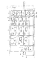
これを図11の平面図に示し、以下に説明する。この基板処理装置は、未処理の複数枚(例えば25枚)の基板W又は後述する処理部104での処理が完了した基板Wが収納されるカセットCが複数個載置されるカセット載置台101と、各カセットCの前を水平移動し、各カセットCと後述する処理部104間で基板Wの受け渡しを行う搬送機構108aとを備えたインデクサ103と、複数個の処理部104と、複数個の処理部104間で基板Wを搬送する経路である基板主搬送経路105と、処理部104および外部処理装置107間で基板Wの受け渡しを中継するインターフェイス106とから構成されている。
【0004】
外部処理装置107は、基板処理装置とは別体の装置であって、基板処理装置のインターフェイス106に対して着脱可能に構成されている。基板処理装置が、上述したレジスト塗布および現像処理を行う装置である場合、この外部処理装置107は、基板Wの露光処理を行う露光装置となる。
【0005】
また、基板主搬送経路105上を搬送する主搬送機構108bと、インターフェイス106の搬送経路上を搬送する搬送機構108cとがそれぞれ配設されている。その他に、インデクサ103と基板主搬送経路105との連結部には載置台109a、基板主搬送経路105とインターフェイス106との連結部には載置台109bがそれぞれ配設されている。
【0006】
上述した基板処理装置において、以下の手順で基板処理が行われる。未処理の基板Wを収納したカセットCから1枚の基板を搬送機構108aが取り出して、主搬送機構108bに基板Wを渡すために、載置台109aまで搬送する。主搬送機構108bは、載置台109aに載置された基板Wを受け取った後、各処理部104内で所定の処理(例えば、レジスト塗布などの処理)をそれぞれ行うために、それらの処理部104に基板Wをそれぞれ搬入する。所定の各処理がそれぞれ終了すると、主搬送機構108bはそれらの処理部104から基板Wをそれぞれ搬出して、次の処理を行うために別の処理部104(例えば、熱処理)に基板Wを搬入する。
【0007】
このように露光前の一連の処理が終了すると、主搬送機構108bは、処理部104で処理された基板Wを載置部109bまで搬送する。搬送機構108cに基板Wを渡すために、上述した載置台109bに基板Wを載置する。搬送機構108cは、載置台109bに載置された基板Wを受け取った後、外部処理装置107まで搬送する。外部処理装置107に搬入して、所定の処理(例えば、露光処理などの処理)が終了すると、搬送機構108cは外部処理装置107から基板Wを搬出して、載置部109bまで搬送する。後は、主搬送機構108bによって各処理部104に基板が搬送され、露光後の一連の加熱処理、冷却処理、現像処理が行われ、全ての処理を完了した基板は搬送機構108aを通じて所定のカセットCに搬入される。そして、カセット載置台101から払い出されて、一連の基板処理が終了する。
【0008】
【発明が解決しようとする課題】
しかしながら、このような構成を有する従来例の場合には、次のような問題がある。
すなわち、従来の基板処理装置は、基板主搬送経路105に沿って走行する1台の主搬送機構108bが全ての処理部104に対して基板Wを受け渡しするので、主搬送機構108bの動作速度の関係から、短時間の間に多くの処理部104に対してアクセスすることができない。そのため従来の基板処理装置は、最近のスループット向上の要請に応えることができないという問題点がある。
【0009】
本発明は、このような事情に鑑みてなされたものであって、スループットを向上することができる基板処理装置を提供することを主たる目的としている。
【0010】
【課題を解決するための手段】
本発明は、このような目的を達成するために、次のような構成をとる。
すなわち、請求項1記載の発明は、基板に対して一連の薬液処理と熱処理とを行う基板処理装置において、薬液処理を行う薬液処理部と、前記薬液処理に関連した熱処理を行う熱処理部と、前記薬液処理部および前記熱処理部に対して基板の受け渡しをする単一の主搬送機構とを含んで単一の処理ブロックを構成し、異なる薬液処理ごとに構成された複数個の処理ブロックを並設してあり、前記各処理ブロックの主搬送機構は、基板の受け渡しを行うために基板を載置する基板載置部を介して、互いに基板の受け渡しを行い、前記基板載置部は、ある処理ブロックから基板を払出すための払出し用基板載置部と、ある処理ブロックへ基板を戻すための戻し用基板載置部との少なくとも2つの基板載置部を上下に近接して設けられて構成されるとともに、前記基板は、並設された各処理ブロックを往路と復路を通じて、前記各処理ブロックの単一の主搬送機構によって往復して移送され、前記主搬送機構を使って基板を特定の位置から別の位置に搬送する工程を1搬送工程とした場合に、前記基板の前記往路における移送は、前記主搬送機構が往路の上流側にある払出し用基板載置部と戻し用基板載置部に対して1搬送工程で基板の受け渡しを行うことによって、前記主搬送機構の各々が前記基板を前記往路の上流側にある払出し用基板載置部から次々と受け取ると共に、前記主搬送機構が往路の下流側にある払出し用基板載置部と戻し用基板載置部に対して1搬送工程で基板の受け渡しを行うことによって、前記主搬送機構の各々が前記基板を前記往路の下流側にある払出し用基板載置部に次々と載置することで行われ、前記基板の前記復路における移送は、前記主搬送機構が復路の上流側にある払出し用基板載置部と戻し用基板載置部に対して1搬送工程で基板の受け渡しを行うことによって、前記主搬送機構の各々が前記基板を前記復路の上流側にある戻し用基板載置部から次々と受け取ると共に、前記主搬送機構が復路の下流側にある払出し用基板載置部と戻し用基板載置部に対して1搬送工程で基板の受け渡しを行うことによって、前記主搬送機構の各々が前記基板を前記復路の下流側にある戻し用基板載置部に次々と載置することで行われることを特徴としている。
ことを特徴としている。
【0011】
請求項1記載の発明によれば、基板に対する一連の薬液処理と熱処理とが並設された複数個の処理ブロックで順に行われる。各処理ブロックでは、各々の主搬送機構が薬液処理部および熱処理部に対して基板の受け渡しを並行して行う。つまり、各処理ブロックの主搬送機構が同時並行的に作動することによって、各処理部に対する基板の受け渡しの速度が等価的に向上するので、基板処理装置のスループットを向上させることができる。また、請求項1記載の発明によれば、基板の受け渡しを行うために基板を載置する基板載置部を介して、互いに基板の受け渡しを行う。このようにすれば、ある処理ブロックの主搬送機構は、その処理ブロックでの処理が終わった基板を基板載置部に置くだけで、次の処理に進むことができる。つまり、隣接する処理ブロックの主搬送機構の動作状態にかかわらず、処理を進めることができるので、基板処理装置のスループットを一層向上させることができる。そして、請求項1記載の発明によれば、ある処理ブロックから基板を払出すための払出し用基板載置部と、ある処理ブロックへ基板を戻すための戻し用基板載置部との少なくとも2つの基板載置部から構成される。このように構成すれば、2つの基板載置部を使って、ある処理ブロックからの基板の払出し(搬出)と、ある処理ブロックへの基板の戻し(搬入)を略同時に行うことができるので、基板処理装置のスループットを一層向上させることができる。さらに、請求項1記載の発明よれば、払出し用基板載置部と戻し用基板載置部は、上下に近接して設けられているので、単一の主搬送機構を使って基板を搬入・搬出するときの主搬送機構の移動距離が短くなるので、基板処理装置のスループットを一層向上させることができる。
【0012】
上記の基板処理装置において、前記各処理ブロックの主搬送機構が負担する搬送工程数のバラツキは2搬送工程以内であることが好ましい(請求項2記載の発明)。
【0013】
複数個の搬送機構を使って一連の基板処理を順に進める場合、特定の搬送機構の搬送負担が多くなって、所定枚数以上の基板を単位時間あたりに処理できなくなると、他の搬送機構に余裕があっても、基板処理装置全体としては、それ以上の処理効率の向上を望めない。本発明によれば、各処理ブロックの主搬送機構が負担する搬送工程数のバラツキは2搬送工程以内であるので、特定の主搬送機構だけが早く搬送処理の限界に陥ることが回避でき、結果として、基板処理装置のスループットを向上させることができる。
【0014】
(削除)
【0015】
(削除)
【0016】
(削除)
【0017】
本発明において、前記基板載置部を設ける位置は特に限定されないが、処理ブロック間に雰囲気遮断のために隔壁が設けられている場合には、基板載置部は前記隔壁を部分的に貫通して設けられる(請求項3記載の発明)。これにより、隣接する処理ブロック間の雰囲気の相互影響を最小限にして、処理ブロック間の基板の受け渡しを円滑に行うことができる。
【0018】
前記基板載置部に、基板の有無を検出するセンサを設けるのが好ましい(請求項4記載の発明)。センサの検出信号に基づき、主搬送機構が基板載置部に対して基板を受け渡しできるか否かを判断することができるので、同じ基板載置部に重ねて基板を載置するなどのトラブルを防止することができるとともに、主搬送機構によるいわゆる「空取り」などの無駄な動作を省くこともできる。
【0019】
処理ブロック内における薬液処理部、熱処理部、および主搬送機構のレイアウトは任意であるが、好ましくは、主搬送機構を挟んで薬液処理部と熱処理部とが対向して配置される(請求項5記載の発明)。このように配置すれば、薬液処理部と熱処理部とが隔たるので、薬液処理部が熱処理部から受ける熱的影響を抑えることができる。
【0020】
本発明において、好ましくは、前記薬液処理部が複数個あって、これらが上下に積層配置されており、かつ、前記熱処理部が複数個あって、これらが上下に積層配置されている(請求項6記載の発明)。このように薬液処理部と熱処理部を多段に構成すれば、基板処理装置の占有スペースを小さくすることができる。
【0021】
さらに、好ましくは、前記熱処理部は、上下に積層配置されたものが複数列にわたり並設される(請求項7記載の発明)。このように構成すれば、熱処理部のメンテナンスが容易であり、また熱処理部に必要なダクト配管や給電設備をあまり高い位置にまで引き延ばす必要がなくなる。
【0022】
本発明において、熱処理部の構成は特に限定されないが、好ましくは、熱処理部は、基板を載置して加熱処理をする加熱プレートと、この加熱プレートから離れた上方位置または下方位置に基板を載置しておく基板仮置部と、前記加熱プレートと基板仮置部との間で基板を搬送する熱処理部用のローカル搬送機構とを備えた基板仮置部付きの熱処理部で構成される(請求項8記載の発明)。このような基板仮置部付きの熱処理部によれば、主搬送機構の動作に無関係に、熱処理された基板を加熱プレートから基板仮置部に移して待機させておくことができるので、主搬送機構が他の動作を行っていたために、あるいは故障のために、基板が過度に加熱されるという事態を防止することができる。なお、熱処理部のすべてが、基板仮置部付きの熱処理部である必要はなく、過度の加熱を防止する必要性の高い熱処理部に用いればよい。
【0023】
前記基板仮置部付き熱処理部のローカル搬送機構は、好ましくは、前記加熱プレートから基板仮置部へ基板を搬送する過程で基板を冷却する冷却手段を備える(請求項9記載の発明)。このように構成すれば、加熱プレートから取り上げられた基板が即座に冷却される。換言すれば、搬送途中に余熱で熱せられることがないので、基板の加熱時間を厳密にコントロールすることができ、基板処理の品質を向上することができる。
【0024】
さらに、前記主搬送機構は、前記基板仮置部に対して基板の受け渡しを行うのが好ましい(請求項10記載の発明)。主搬送機構が熱処理部の加熱プレートにアクセスすると、主搬送機構の温度が上昇し、主搬送機構によって搬送される基板に熱的悪影響を与えることがある。これに対し、主搬送機構が基板仮置部に対して基板の受け渡しを行うように構成すれば、主搬送機構の温度上昇を防止することができ、基板処理の品質を一層向上することができる。
【0025】
さらに好ましくは、前記基板仮置部付きの熱処理部の少なくとも加熱プレートは筐体で覆われており、この筐体内の加熱プレートに対して前記ローカル搬送機構が基板を受け渡すために前記筐体に設けられた開口部は、前記主搬送機構が配置された側とは反対側に位置している(請求項11記載の発明)。このようにすれば、開口部から漏れ出た熱雰囲気が主搬送機構に及ぼす影響が少なくなるので、主搬送機構の温度上昇を一層軽減することができる。
【0026】
また、本発明は、基板に対して一連の薬液処理と熱処理とを行う基板処理装置において、 基板を多段に収容する複数個のカセットを載置するカセット載置台と、各カセットから未処理の基板を順に取り出すとともに、各カセットへ処理済の基板を順に収納するインデクサ用搬送機構とを備えたインデクサブロックと、基板表面に反射防止膜を塗布形成する反射防止膜用塗布処理部と、反射防止膜の塗布形成に関連して基板を熱処理する反射防止膜用熱処理部と、前記反射防止膜用塗布処理部および反射防止膜用熱処理部に対して基板の受け渡しをする第1の主搬送機構とを備え、前記インデクサブロックに隣接して設けられる反射防止膜用処理ブロックと、反射防止膜が塗布形成された基板にフォトレジスト膜を塗布形成するレジスト膜用塗布処理部と、フォトレジスト膜の塗布形成に関連して基板を熱処理するレジスト膜用熱処理部と、前記レジスト膜用塗布処理部およびレジスト膜用熱処理部に対して基板の受け渡しをする第2の主搬送機構とを備え、前記反射防止膜用処理ブロックに隣接して設けられるレジスト膜用処理ブロックと、フォトレジスト膜が塗布形成され、さらに露光された基板に現像処理をする現像処理部と、現像処理に関連して基板を熱処理する現像用熱処理部と、前記現像処理部および現像用熱処理部に対して基板の受け渡しをする第3の主搬送機構とを備え、前記レジスト膜用処理ブロックに隣接して設けられる現像処理ブロックと、前記現像処理ブロックに隣接して設けられ、本基板処理装置とは別体の外部装置である露光装置に対して基板の受け渡しをするインターフェイス用搬送機構を備えたインターフェイスブロックとを備え、前記インデクサブロックのインデクサ用搬送機構と前記反射防止膜用処理ブロックの第1の主搬送機構とは、基板の受け渡しを行うために基板を載置する基板載置部を介して、互いに基板の受け渡しを行い、同様に、前記第1の主搬送機構と前記レジスト膜用処理ブロックの第2の主搬送機構、前記第2の主搬送機構と前記現像処理ブロックの第3の主搬送機構、前記第3の主搬送機構と前記第4の主搬送機構、および前記第4の主搬送機構と前記インターフェイスブロックのインターフェイス用搬送機構のそれぞれは、基板の受け渡しを行うために基板を載置する基板載置部を介して、互いに基板の受け渡しを行い、前記基板載置部は、ある処理ブロックから基板を払出すための払出し用基板載置部と、ある処理ブロックへ基板を戻すための戻し用基板載置部との少なくとも2つの基板載置部を上下に近接して設けられて構成されるとともに、前記基板は、並設された各処理ブロックを往路と復路を通じて、前記各処理ブロックの単一の主搬送機構によって往復して移送され、前記主搬送機構を使って基板を特定の位置から別の位置に搬送する工程を1搬送工程とした場合に、前記基板の前記往路における移送は、前記主搬送機構が往路の上流側にある払出し用基板載置部と戻し用基板載置部に対して1搬送工程で基板の受け渡しを行うことによって、前記主搬送機構の各々が前記基板を前記往路の上流側にある払出し用基板載置部から次々と受け取ると共に、前記主搬送機構が往路の下流側にある払出し用基板載置部と戻し用基板載置部に対して1搬送工程で基板の受け渡しを行うことによって、前記主搬送機構の各々が前記基板を前記往路の下流側にある払出し用基板載置部に次々と載置することで行われ、前記基板の前記復路における移送は、前記主搬送機構が復路の上流側にある払出し用基板載置部と戻し用基板載置部に対して1搬送工程で基板の受け渡しを行うことによって、前記主搬送機構の各々が前記基板を前記復路の上流側にある戻し用基板載置部から次々と受け取ると共に、前記主搬送機構が復路の下流側にある払出し用基板載置部と戻し用基板載置部に対して1搬送工程で基板の受け渡しを行うことによって、前記主搬送機構の各々が前記基板を前記復路の下流側にある戻し用基板載置部に次々と載置することで行われることを特徴とする(請求項12の発明)。
【0027】
本発明によれば、インデクサブロックから取り出された未処理の基板が反射防止膜用処理ブロックに渡され、この処理ブロックで基板上に反射防止膜が塗布形成される。反射防止膜が塗布形成された基板は、レジスト膜用処理ブロックに渡され、この処理ブロックでフォトレジスト膜が塗布形成される。フォトレジスト膜が塗布形成された基板は、現像処理ブロックを素通りしてインターフェイスブロックに渡される。インターフェイスブロックは、その基板を外部装置である露光装置に渡す。露光処理された基板は、インターフェイスブロックを介して、現像処理ブロックに渡され、この処理ブロックで現像処理される。現像処理された基板は、レジスト膜用処理ブロックと反射防止膜用処理ブロックを素通りして、インデクサブロックに返される。インデクサブロックは、処理済みの基板をカセットに収納する。各処理ブロックでは、各々の主搬送機構が各々の薬液処理部(反射防止膜用塗布処理部、レジスト膜用塗布処理部、現像処理部)および熱処理部に対して基板の受け渡しを並行して行う。つまり、各処理ブロックの主搬送機構が同時並行的に作動することによって、各処理部に対する基板の受け渡しの速度が等価的に向上するので、基板処理装置のスループットを向上させることができる。また、本発明の基板処理装置において、前記インデクサブロックのインデクサ用搬送機構と前記反射防止膜用処理ブロックの第1の主搬送機構とは、基板の受け渡しを行うために基板を載置する基板載置部を介して、互いに基板の受け渡しを行い、同様に、前記第1の主搬送機構と前記レジスト膜用処理ブロックの第2の主搬送機構、前記第2の主搬送機構と前記現像処理ブロックの第3の主搬送機構、前記第3の主搬送機構と前記第4の主搬送機構、および前記第4の主搬送機構と前記インターフェイスブロックのインターフェイス用搬送機構のそれぞれは、基板の受け渡しを行うために基板を載置する基板載置部を介して、互いに基板の受け渡しを行う。このようにすれば、各処理ブロックの主搬送機構は、その処理ブロックでの処理が終わった基板を基板載置部に置くだけで、次の処理に進むことができるので、基板処理装置のスループットを一層向上させることができる。
【0028】
上記の基板処理装置において、少なくとも前記インデクサブロックと前記反射防止膜用処理ブロックとの間は、基板受け渡し用の開口部位を除いて隔壁で区画され、かつ、反射防止膜用処理ブロック内の気圧がインデクサブロック内の気圧よりも高くなるように設定するのが好ましい(請求項13記載の発明)。このように構成すれば、インデクサブロック内の雰囲気が反射防止膜用処理ブロックに流入しないので、外部の雰囲気の影響を受けずに処理を行うことができ、処理の品質を向上させることができる。
【0029】
さらに、上記の基板処理装置において、好ましくは、前記現像処理ブロックの熱処理部は、基板を載置して加熱処理をする加熱プレートと、この加熱プレートから離れた上方位置または下方位置に基板を載置しておく基板仮置部と、前記加熱プレートと基板仮置部との間で基板を搬送する熱処理部用のローカル搬送機構とを備えた基板仮置部付きの熱処理部を含み、前記インターフェイスブロックはさらに、フォトレジストが塗布された基板の周縁部を露光するエッジ露光部と、前記基板仮置部付きの熱処理部および前記エッジ露光部に対して基板を受け渡しする第4の主搬送機構とを備える(請求項14記載の発明)。この構成によれば、フォトレジスト膜が塗布形成された基板は、現像処理ブロックを素通りして、インターフェイスブロックの第4の主搬送機構に受け渡されて、エッジ露光部に搬入される。エッジ露光された基板は、インターフェイスブロックのインターフェイス用搬送機構によって外部装置である露光装置に渡される。露光された基板はインターフェイス搬送機構用搬送機構から第4の主搬送機構に受け渡されて、基板仮置部付きの熱処理部に搬入される。熱処理された基板は現像処理ブロックに渡されて現像処理される。露光された基板を基板仮置部付きの熱処理部へ搬入するための搬送を、現像処理ブロックの第3の主搬送機構に依らず、独立した第4の主搬送機構で行っているので、仮に現像処理ブロックに異常が生じて第3の主搬送機構が停止しても、露光後の加熱を確実に行うことができる。フォトレジストとして化学増幅型フォトレジストを用いた場合、露光後の加熱を速やかに行う必要があるので、この点で本発明は好適である。
【0030】
この場合、前記熱処理部用のローカル搬送機構が、前記加熱プレートから基板仮置部へ基板を搬送する過程で基板を冷却する冷却手段を備えると(請求項15記載の発明)、露光後の加熱時間を一層厳密にコントロールできるので好ましい。
【0031】
(削除)
【0032】
さらに、本発明の基板処理装置において、好ましくは、前記インターフェイスブロックは、露光機が基板の受け入れをできないときに、露光処理前の基板を収納する送り用バッファと、露光処理後の基板を現像処理できないときに、現像処理前の基板を収納する戻りバッファと備え、前記インターフェイス用搬送機構は、露光機が基板の受け入れをできないときに、露光処理前の基板を前記送り用バッファに収納し、前記第4の主搬送機構は、露光処理後の基板を現像処理できないときに、現像処理前の基板を、前記現像処理ブロックの基板仮置部付きの熱処理部で熱処理した後に、前記戻りバッファに収納する(請求項16記載の発明)。この構成によれば、現像処理ブロックなどに異常が生じて基板の現像処理ができない場合に、露光後の加熱処理を行った後に戻りバッファへ収納するので、露光された基板が熱処理を受けずに長時間放置されることがない。これは露光後の加熱を速やかに行う必要がある化学増幅型フォトレジストを用いた場合に好適である。
【0033】
(削除)
【0034】
(削除)
【0035】
(削除)
【0036】
また、本発明は、請求項1または請求項13に記載の基板処理装置において、処理ブロックの各々には、コントローラが備えられており、コントローラの各々が主搬送機構の各々を独立に制御することを特徴とするものである(請求項17記載の発明)。
【0037】
また、本発明は、薬液処理を行う薬液処理部と、前記薬液処理に関連した熱処理を行う熱処理部と、前記薬液処理部および前記熱処理部に対して基板の受け渡しをする単一の主搬送機構とを含んで単一の被制御ユニットを構成し、異なる薬液処理ごとに構成された複数個の被制御ユニットを並設してある基板処理装置であって、前記各被制御ユニットの主搬送機構は、基板の受け渡しを行うために基板を載置する基板載置部を介して、互いに基板の受け渡しを行い、前記基板載置部は、ある被制御ユニットから基板を払出すための払出し用基板載置部と、ある被制御ユニットへ基板を戻すための戻し用基板載置部との少なくとも2つの基板載置部を上下に近接して設けられて構成されており、前記主搬送機構を使って基板を特定の位置から別の位置に搬送する工程を1搬送工程とした場合に、前記各被制御ユニットの主搬送機構が負担する搬送工程数のバラツキは2搬送工程以内であるとともに、前記基板は、並設された各被制御ユニットを往路と復路を通じて、前記各被制御ユニットの単一の主搬送機構によって往復して移送され、前記基板の前記往路における移送は、前記主搬送機構が往路の上流側にある払出し用基板載置部と戻し用基板載置部に対して1搬送工程で基板の受け渡しを行うことによって、前記主搬送機構の各々が前記基板を前記往路の上流側にある払出し用基板載置部から次々と受け取ると共に、前記主搬送機構が往路の下流側にある払出し用基板載置部と戻し用基板載置部に対して1搬送工程で基板の受け渡しを行うことによって、前記主搬送機構の各々が前記基板を前記往路の下流側にある払出し用基板載置部に次々と載置することで行われ、前記基板の前記復路における移送は、前記主搬送機構が復路の上流側にある払出し用基板載置部と戻し用基板載置部に対して1搬送工程で基板の受け渡しを行うことによって、前記主搬送機構の各々が前記基板を前記復路の上流側にある戻し用基板載置部から次々と受け取ると共に、前記主搬送機構が復路の下流側にある払出し用基板載置部と戻し用基板載置部に対して1搬送工程で基板の受け渡しを行うことによって、前記主搬送機構の各々が前記基板を前記復路の下流側にある戻し用基板載置部に次々と載置することで行われることを特徴とする(請求項18記載の発明)。
【0038】
また、本発明は、請求項18に記載の基板処理装置において、被制御ユニットの各々には、コントローラが備えられており、コントローラの各々が主搬送機構の各々を独立に制御することを特徴とするものである(請求項19記載の発明)。
【0039】
本発明によれば、各被制御ユニットの主搬送機構が負担する搬送工程数のバラツキは2搬送工程以内であるので、特定の主搬送機構だけが早く搬送処理の限界に陥ることが回避でき、結果として、基板処理装置のスループットを向上させることができる。
【0040】
なお、本発明において、各被制御ユニット(または、請求項2記載の発明の各処理ブロック)の主搬送機構は、完全に同数の搬送工程を負担する必要はない。基板処理装置のスループットを向上し得る程度に、主要な被制御ユニットの主搬送機構の搬送負担が均等化されていればよい。現実的には、各主搬送機構が負担する搬送工程数のバラツキは、2搬送工程以内が好ましい。また、特定の被制御ユニットにおける処理時間を厳密に管理する必要がある場合や、その被制御ユニットにオプションとして別の処理部が追加されることが予想される場合には、その被制御ユニットの主搬送機構の搬送負担に余裕をもたせる意味で、その搬送負担を他の被制御ユニットに比べて故意に低く設定してもよい。
【0041】
【発明の実施の形態】
以下、図面を参照して本発明の実施例を説明する。
図1は実施例に係る基板処理装置の平面図、図2はその正面図、図3は熱処理部の正面図である。
【0042】
ここでは、半導体ウエハ(以下、単に「基板」という)に、反射防止膜やフォトレジスト膜を塗布形成するとともに、露光された基板に現像処理などの薬液処理を行う基板処理装置を例に採って説明する。もちろん、本発明に係る基板処理装置が取り扱い得る基板は、半導体ウエハに限らず、液晶表示器用のガラス基板など種々の基板を含む。また、薬液処理は、フォトレジスト膜などの塗布形成処理や現像処理に限らず、種々の薬液処理を含む。
【0043】
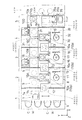
図1を参照する。本実施例に係る基板処理装置は大きく分けて、インデクサブロック1と、基板に対して所要の薬液処理を行う3つの処理ブロック(具体的には反射防止膜用処理ブロック2、レジスト膜用処理ブロック3、および現像処理ブロック4)と、インターフェイスブロック5とからなり、これらのブロックを並設して構成されている。インターフェイスブロック5には、本実施例に係る基板処理装置とは別体の外部装置である露光装置(ステッパー)STPが並設される。以下、各ブロックの構成を説明する。
【0044】
まず、インデクサブロック1について説明する。インンデクサブロック1は、基板Wを多段に収納するカセットCからの基板の取り出しや、カセットCへの基板Wの収納を行う機構である。具体的には、複数個のカッセトCを並べて載置するカセット載置台6と、各カセットCから未処理の基板Wを順に取り出すとともに、各カセットCへ処理済の基板Wを順に収納するインデクサ用搬送機構7とを備えている。インデクサ用搬送機構7は、カセット載置台6に沿って(Y方向に)水平移動可能な可動台7aを備えている。この可動台7aに基板Wを水平姿勢で保持する保持アーム7bが搭載されている。保持アーム7bは、可動台7a上を昇降(Z方向)移動、水平面内の旋回移動、および旋回半径方向に進退移動可能に構成されている。
【0045】
上述したインデクサブロック1に隣接して反射防止膜処理ブロック2が設けられている。図4に示すように、インデクサブロック1と反射防止膜処理ブロック2との間には、雰囲気遮断用の隔壁13が設けられている。この隔壁13にインデクサブロック1と反射防止膜処理ブロック2との間で基板Wの受け渡しを行うために基板Wを載置する2つの基板載置部PASS1、PASS2が上下に近接して設けられている。上側の基板載置PASS1はインデクサブロック1から反射防止膜処理ブロック2へ基板Wを払い出すために、下側の基板載置部PASS2は反射防止膜処理ブロック2からインデクサブロック1へ基板Wを戻すために、それぞれ設けられている。基板載置部PASS1、PASS2は、隔壁13を部分的に貫通して設けられている。なお、基板載置部PASS1、PASS2は、固定設置された複数本の支持ピンから構成されており、この点は後述する他の基板載置部PASS3〜PASS10も同様である。また、基板載置部PASS1、PASS2には、基板Wの有無を検出する図示しない光学式のセンサが設けられており、各センサの検出信号に基づいてインデクサ用搬送機構7や、後述する反射防止膜用処理ブロック2の第1の主搬送機構10Aが、基板載置部PASS1、PASS2に対して基板を受け渡しできる状態であるかどうかを判断するようになっている。同様のセンサは他の基板載置部PASS3〜PASS10にも設けられている。
【0046】
反射防止膜処理ブロック2について説明する。反射防止膜処理ブロック2は、露光時に発生する定在波やハレーションを減少させるために、フォトレジスト膜の下部に反射防止膜を塗布形成するための機構である。具体的には、基板Wの表面に反射防止膜を塗布形成する反射防止膜用塗布処理部8と、反射防止膜の塗布形成に関連して基板Wを熱処理する反射防止膜用熱処理部9と、反射防止膜用塗布処理部8および反射防止膜用熱処理部9に対して基板Wの受け渡しをする第1の主搬送機構10Aとを備える。
【0047】
反射防止膜処理ブロック2は、第1の主搬送機構10Aを挟んで反射防止膜用塗布処理部8と反射防止膜用熱処理部9とが対向して配置されている。具体的には、塗布処理部8が装置正面側に、熱処理部9が装置背面側に、それぞれ位置している。このように薬液処理部と熱処理部とを主搬送機構を挟んで対向配置する点は、他のレジスト膜用処理ブロック3および現像処理ブロック4においても同様である。このような配置にすれば、薬液処理部と熱処理部とが隔たるので、薬液処理部が熱処理部から受ける熱的影響を抑えることができる。また、本実施例では、熱処理部9の正面側に図示しない熱隔壁を設けて、反射防止膜用塗布処理部8への熱的影響を回避している。同様な熱隔壁は、他のレジスト膜用処理ブロック3および現像処理ブロック4にも設けられている。
【0048】
反射防止膜用塗布処理部8は、図2に示すように、同様の構成を備えた3つの反射防止膜用塗布処理部8a〜8c(以下、特に区別しない場合は符号「8」で示す)を上下に積層配置して構成されている。各塗布処理部8は、基板Wを水平姿勢で吸着保持して回転するスピンチャック11や、このスピンチャック11上に保持された基板W上に反射防止膜用の塗布液を供給するノズル12などを備えている。
【0049】
反射防止膜用熱処理部9は、図3に示すように、基板Wを所定の温度にまで加熱する複数個の加熱プレートHP、加熱された基板Wを常温にまで冷却する複数個の冷却プレートCP、レジスト膜と基板Wとの密着性を向上させるためにHMDS(ヘキサメチルジシラザン)の蒸気雰囲気で基板Wを熱処理する複数個のアドヒージョン処理部AHLなどの熱処理部を含む。これらの熱処理部9の下部には、ヒータコントローラ(CONT)が配設され、また熱処理部9の上部(図3中に「×」印で示した個所)には配管配線部や、予備の空きスペースが割り当てられている。
【0050】
反射防止膜用熱処理部9は、各熱処理部(HP,CP,AHL)を上下に積層配置して構成されているとともに、積層配置された一群の熱処理部が複数例(本実施例では2列)にわたり並設されている。薬液処理部を上下に積層配置している点、および上下に積層配置した一群の熱処理部を複数列にわたり並設している点は、他のレジスト膜用処理ブロック3および現像処理ブロック4においても同様である。
【0051】
上述したように各処理ブロック2〜4で薬液処理部や熱処理部を上下に積層配置することにより、基板処理装置の占有スペースを小さくすることができる。また、積層配置した一群の記熱処理部を複数列のわたり並設することにより、熱処理部のメンテナンスが容易になるとともに、熱処理部に必要なダクト配管や給電設備をあまり高い位置にまで引き延ばす必要がなくなるという利点がある。
【0052】
第1の主搬送機構10Aについて説明する。なお、後述する他のレジスト膜用処理ブロック3、現像処理ブロック4、およびインターフェイスブロック5にそれぞれ備えられた第2、第3、第4の各主搬送機構10B、10C、10Dも同様に構成されている。以下、第1〜第4の主搬送機構10A〜10Dを特に区別しない場合は、主搬送機構10として説明する。
【0053】
図6を参照する。同図(a)は主搬送機構10の平面図、(b)はその正面図である。主搬送機構10は、基板Wを水平姿勢で保持する2個の保持アーム10a、10bを上下に近接して備えている。保持アーム10a、10bは、先端部が「C]の字状になっており、この「C」の字状のアームの内側から内方に突き出た複数本のピン10cで基板Wの周縁を下方から支持するようになっている。主搬送機構10の基台10dは装置基台に対して固定設置されている。この基台10d上に螺軸10eが回転可能に立設支持されている。基台10dに螺軸10eを回転駆動するモータ10fが設けられている。螺軸10eに昇降台10gが螺合されており、モータ10fが螺軸10eを回転駆動することにより、昇降台10gがガイド軸10jに案内されて昇降移動するようになっている。昇降台10g上にアーム基台10hが縦軸心周りに旋回可能に搭載されている。昇降台10gにはアーム基台10hを旋回駆動するモータ10iが設けられている。アーム基台10h上に上述した2つの保持アーム10a、10bが上下に配設されている。各保持アーム10a、10bは、アーム基台10h内に装備された駆動機構(図示せず)によって、各々が独立してアーム基台10hの旋回半径方向に進退移動可能に構成されている。
【0054】
上述した反射防止膜処理ブロック2に隣接してレジスト膜処理ブロック3が設けられている。図4に示すように、反射防止膜処理ブロック2とレジスト膜処理ブロック3との間にも、雰囲気遮断用の隔壁13が設けられている。この隔壁13に反射防止膜処理ブロック2とレジスト膜処理ブロック3との間で基板Wの受け渡しを行うための2つの基板載置部PASS3、PASS4が上下に近接して設けられている。上述した基板載置部PASS1、PASS2の場合と同様に、上側の基板載置部PASS3が基板Wの払出し用、下側の基板載置部PASS4が基板Wの戻し用になっているとともに、これらの基板載置部PASS3、PASS4は隔壁13を部分的に貫通している。また、基板載置部PASS3、PASS4の下側には、基板Wを大まかに冷却するために水冷式の2つの冷却プレートWCPが隔壁13を貫通して上下に設けられている。
【0055】
レジスト膜用処理ブロック3について説明する。レジスト膜用処理ブロック3は、反射防止膜が塗布形成された基板W上にフォトレジスト膜を塗布形成する機構である。なお、本実施例では、フォトレジストとして化学増幅型レジストを用いている。レジスト膜用処理ブロック3は、反射防止膜が塗布形成された基板Wにフォトレジスト膜を塗布形成するレジスト膜用塗布処理部15と、フォトレジスト膜の塗布形成に関連して基板を熱処理するレジスト膜用熱処理部16と、レジスト膜用塗布処理部15およびレジスト膜用熱処理部16に対して基板Wの受け渡しをする第2の主搬送機構10Bとを備える。
【0056】
レジスト膜用塗布処理部15は、図2に示すように、同様の構成を備えた3つのレジスト膜用塗布処理部15a〜15c(以下、特に区別しない場合は符号「15」で示す)を上下に積層配置して構成されている。各塗布処理部15は、基板Wを水平姿勢で吸着保持して回転するスピンチャック17や、このスピンチャック17上に保持された基板W上にレジスト膜用の塗布液を供給するノズル18などを備えている。
【0057】
レジスト膜用熱処理部16は、図3に示すように、基板Wを所定の温度にまで加熱する基板仮置部付きの複数個の加熱部PHP、基板Wを常温にまで高い精度で冷却する複数個の冷却プレートCPなどの熱処理部を含む。各熱処理部が上下に積層されるとともに並列配置されている点は、反射防止膜用処理ブロック2の場合と同様である。
【0058】
基板仮置部付きの加熱部PHPについて説明する。
図7を参照する。同図(a)は加熱部PHPの破断側面図、(b)は破断平面図である。加熱部PHPは、基板Wを載置して加熱処理をする加熱プレートHPと、この加熱プレートHPから離れた上方位置または下方位置(本実施例では上方位置)に基板Wを載置しておく基板仮置部19と、加熱プレートHPと基板仮置部19との間で基板Wを搬送する熱処理部用のローカル搬送機構20とを備えている。加熱プレートHPには、プレート表面に出没する複数本の可動支持ピン21が設けられている。加熱プレートHPの上方には加熱処理時に基板Wを覆う昇降自在の上蓋22が設けられている。基板仮置部19には基板Wを支持する複数本の固定支持ピン23が設けられている。
【0059】
ローカル搬送機構20は、基板Wを水平姿勢で保持する保持プレート24を備え、この保持プレート24がネジ送り駆動機構25によって昇降移動されるとともに、ベルト駆動機構26によって進退移動されるようになっている。保持プレート24は、これが加熱プレートHPや基板仮置部19の上方に進出したときに、可動支持ピン21や固定支持ピン23と干渉しなように複数本のスリット24aが形成されている。また、ローカル搬送機構20は、加熱プレートHPから基板仮置部19へ基板Wを搬送する過程で基板を冷却する手段を備えている。この冷却手段は、例えば保持プレート24の内部に冷却水流路24bを設け、この冷却水流路24bに冷却水を流通させることによって構成されている。
【0060】
上述したローカル搬送機構20は、加熱プレートHPおよび基板仮置部19を挟んでは第2の主搬送機構10Bとは反対側、すなわち装置背面側に設置されている。そして、加熱プレートHPおよび基板仮置部19を覆う筐体27の上部、すなわち基板仮置部19を覆う部位には、その正面側に第2の主搬送機構10Bの進入を許容する開口部19aが、その背面側にはローカル搬送機構20の進入を許容する開口部19bが、それぞれ設けられている。また、筐体27の下部、すなわち加熱プレートHPを覆う部位は、その正面側が閉塞し、その背面側にローカル搬送機構20の進入を許容する開口部19cが設けられている。
【0061】
上述した加熱部PHPに対する基板Wの出し入れは以下のようにして行われる。まず、主搬送機構10(レジスト膜用処理ブロック3の場合は、第2の主搬送機構10B)が基板Wを保持して、基板仮置部19の固定支持ピン23の上に基板Wを載置する。続いてローカル搬送機構20の保持プレート24が基板Wの下側に進入してから少し上昇することにより、固定支持ピン23から基板Wを受け取る。基板Wを保持した保持プレート24は筐体27から退出して、加熱プレートHPに対向する位置にまで下降する。このとき加熱プレートHPの可動支持ピン21は下降しているとともに、上蓋22は上昇している。基板Wを保持した保持プレート24は加熱プレートHPの上方に進出する。可動支持ピン21が上昇して基板Wを受け取った後に保持プレート24が退出する。続いて可動支持ピン21が下降して基板Wを加熱プレートHP上に載せるとともに、上蓋22が下降して基板Wを覆う。この状態で基板Wが加熱処理される。加熱処理が終わると上蓋22が上昇するとともに、可動支持ピン21が上昇して基板Wを持ち上げる。続いて保持プレート24が基板Wの下に進出した後、可動支持ピン23が下降することにより、基板Wが保持プレート24に受け渡される。基板Wを保持した保持プレート24が退出して、さらに上昇して基板Wを基板仮置部19に搬送する。この搬送過程で保持プレート24に支持された基板Wが、保持プレート24が有する冷却機能によって冷却される。保持プレート24は、冷却した(常温に戻した)基板Wを基板仮置部19に移載する。この基板Wを主搬送機構10が取り出して搬送する。
【0062】
以上のように、主搬送機構10は、基板仮置部19に対して基板Wの受け渡しをするだけで、加熱プレートHPに対して基板の受け渡しをしないので、主搬送機構10が温度上昇するのを回避することができる。また、加熱プレートHPに基板Wを出し入れするための開口部19cが、主搬送機構10が配置された側とは反対側に位置しているので、開口部19cから漏れ出た熱雰囲気で主搬送機構10が温度上昇することがなく、またレジスト膜用塗布処理部15が開口部19cから漏れ出た熱雰囲気で悪影響を受けることもない。
【0063】
上述したレジスト膜処理ブロック3に隣接して現像処理ブロック4が設けられている。図4に示すように、レジスト膜処理ブロック3と現像処理ブロック4との間にも、雰囲気遮断用の隔壁13が設けられており、この隔壁13に両処理ブロック3、4間で基板Wの受け渡しを行うための2つの基板載置部PASS5,6と、基板Wを大まかに冷却するために水冷式の2つの冷却プレートWCPが上下に積層して設けられている。
【0064】
現像処理ブロック4について説明する。現像処理ブロック4は、露光された基板Wに対して現像処理をする機構である。具体的には、露光された基板Wに現像処理をする現像処理部30と、現像処理に関連して基板を熱処理する現像用熱処理部31と、現像処理部30および現像用熱処理部31に対して基板Wの受け渡しをする第3の主搬送機構10Cとを備える。
【0065】
現像処理部30は、図2に示すように、同様の構成を備えた5つの現像処理部30a〜30e(以下、特に区別しない場合は符号「30」で示す)を上下に積層配置して構成されている。各現像処理部30は、基板Wを水平姿勢で吸着保持して回転するスピンチャック32や、このスピンチャック32上に保持された基板W上に現像液を供給するノズル33などを備えている。
【0066】
現像用熱処理部31は、図3に示すように、各々複数個の加熱プレートHP、基板仮置部付きの加熱部PHP、冷却プレートCPなどの熱処理部を含む。各熱処理部が上下に積層されるとともに並列配置されている点は、他の処理ブロック2、3の場合と同様である。現像用熱処理部31の右側(インターフェイスブロック5に隣接している側)の熱処理部の列には、現像処理ブロック4と、これに隣接するインターフェイスブロック5との間で基板Wの受け渡しを行うための2つの基板載置部PASS7、PASS8が上下に近接して設けられている。上側の基板載置部PASS7が基板Wの払出し用、下側の基板載置部PASS8が基板Wの戻し用になっている。
【0067】
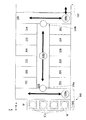
インターフェイスブロック5について説明する。インターフェイスブロック5は、本基板処理装置とは別体の外部装置である露光装置STPに対して基板Wの受け渡しをする機構である。本実施例装置におけるインターフェイスブロック5には、露光装置STPとの間で基板Wの受け渡しをするためのインターフェイス用搬送機構35の他に、フォトレジストが塗布された基板Wの周縁部を露光する2つのエッジ露光部EEWと、現像処理ブロック4内に配設された基板仮置部付きの熱処理部PHPおよびエッジ露光部EEWに対して基板Wを受け渡しする第4の主搬送機構10Dを備えている。
【0068】
エッジ露光部EEWは、図2に示すように、基板Wを水平姿勢で吸着保持して回転するスピンチャック36や、このスピンチャック36上に保持された基板Wの周縁を露光する光照射器37などを備えている。2つのエッジ露光部EEWは、インターフェイスブロック5の中央部に上下に積層配置されている。このエッジ露光部EEWと現像処理ブロック4の熱処理部とに隣接して配置されている第4の主搬送機構10Dは、図6で説明した主搬送機構10と同様の構成を備えている。
【0069】
図2および図5を参照する。図5はインターフェイスブロック5の側面図である。2つのエッジ露光部EEWの下側に、基板戻し用のバッファRBFがあり、さらにその下側に2つの基板載置部PASS9、PASS10が積層配置されている。基板戻し用のバッファRBFは、故障などのために現像処理ブロック4が基板Wの現像処理をすることができない場合に、現像処理ブロック4の加熱部PHPで露光後の加熱処理を行った後に、その基板Wを一時的に収納保管しておくものである。このバッファRBFは、複数枚の基板Wを多段に収納できる収納棚から構成されている。基板載置部PASS9、PASS10は、第4の主搬送機構10Dとインターフェイス用搬送機構35との間で基板Wの受け渡しを行うためのもので、上側が基板払出し用、下側が基板戻し用になっている。
【0070】
インターフェイス用搬送機構35は、図1および図5に示すように、Y方向に水平移動可能な可動台35aを備え、この可動台35a上に基板Wを保持する保持アーム35bを搭載している。保持アーム35bは、昇降・旋回および旋回半径方向に進退移動可能に構成されている。インターフェイス用搬送機構35の搬送経路の一端(図5中に示す位置P1)は、積層された基板載置部PASS9、PASS10の下方にまで延びており、この位置P1で露光装置STPとの間で基板Wの受け渡しを行う。また、搬送経路の他端位置P2では、基板載置部PASS9、PASS10に対する基板Wの受け渡しと、送り用バッファSBFに対する基板Wの収納と取り出しとを行う。送り用バッファSBFは、露光装置STPが基板Wの受け入れをできないときに、露光処理前の基板Wを一時的に収納保管するもので、複数枚の基板Wを多段に収納できる収納棚から構成されている。
【0071】
以上のように構成された基板処理装置は、インデクサブロック1、各処理ブロック2、3、4、およびインターフェイスブロック5内に清浄空気がダウンフローの状態で供給されており、各ブロック内でパーティクルの巻き上がりや気流によるプロセスへの悪影響を回避している。また、各ブロック内は装置の外部環境に対して若干陽圧に保たれて、外部環境からのパーティクルや汚染物質の侵入などを防いでいる。特に、反射防止膜用処理ブロック2内の気圧はインデクサブロク1内の気圧よりも高くなるように設定されている。これにより、インデクサブロック1内の雰囲気が反射防止膜用処理ブロック2に流入しないので、外部の雰囲気の影響を受けずに各処理ブロック2、3、4で処理を行うことができる。
【0072】
次に本実施例に係る基板処理装置の制御系、特に基板搬送に係る制御手法について説明する。
上述したインデクサブロック1、反射防止膜用処理ブロック2、レジスト膜用処理ブロック3、現像処理ブロック4、およびインターフェイスブロック5は、本実施例に係る基板処理装置を機構的に分割した要素である。具体的には、各ブロックは、各々個別のブロック用フレーム(枠体)に組み付けられ、各ブロック用フレームを連結して基板処理装置が構成されている(図8(a)参照)。
【0073】
一方、本発明の特徴の一つとして、基板搬送に係る被制御ユニットの単位を機械的要素である各ブロックとは別に構成している。すなわち、基板に所要の処理を行う処理部と、前記処理部に対して基板の受け渡しをする単一の主搬送機構とを含んで単一の被制御ユニットを構成し、前記被制御ユニットを並設して基板処理装置を構成している。そして、各被制御ユニットの主搬送機構は、基板の受け渡しを行うために基板を載置する基板載置部を介して、互いに基板の受け渡しを行い、かつ、各被制御ユニットの主搬送機構の基板受け渡し動作を少なくとも制御する制御手段を各被制御ユニットごとに備え、各被制御ユニットの制御手段は、前記処理部に対する基板の受け渡しおよび前記基板載置部に対する基板の受け渡しを含む一連の基板搬送に係る制御を、各々独立して行うようになっている。
【0074】
以下、本実施例装置における被制御ユニットの単位を「セル」という。実施例装置の制御系を構成する各セルの配置を図8(b)に示す。
【0075】
インデクサセルC1は、カセット載置台6とインデクサ用搬送機構7とを含む。このセルC1は、結果として機械的に分割した要素であるインデクサブロック1と同じ構成になっている。反射防止膜用処理セルC2は、反射防止膜用塗布処理部8と反射防止膜用熱処理部9と第1の主搬送機構10Aとを含む。このセルC2も、結果として機械的に分割した要素である反射防止膜用処理ブロック2と同じ構成になっている。レジスト膜用処理セルC3は、レジスト膜用塗布処理部15とレジスト膜用熱処理部16と第2の主搬送機構10Bとを含む。このセルC3も、結果として機械的に分割した要素であるレジスト膜用処理ブロック3と同じ構成になっている。
【0076】
一方、現像処理セルC4は、現像処理部30と、露光後加熱に使われる熱処理部(実施例では、加熱部PHP)を除いた現像用熱処理部31と、第3の主搬送機構10Cとを含む。このセルC3は、露光加熱に使われる加熱部PHPを含んでいない点で、機械的に分割した要素である現像処理ブロック4とは異なる構成になっている。
【0077】
露光後加熱用処理セルC5は、露光された基板Wを現像前に加熱処理する露光後加熱用の熱処理部(実施例では、現像処理ブロック4に設けられた加熱部PHP)と、エッジ露光部EEWと、第4の主搬送機構10Dとを含む。このセルC5は、機械的に分割した要素である現像処理ブロック4とインターフェイスブロック5とにまたがるもので、本実施例装置の特徴的なセルである。このように露光後加熱用の熱処理部(加熱部PHP)と第4の主搬送機構10Dとを含んで一つのセルを構成しているので、露光された基板を速やかに加熱部PHPに搬入して熱処理を行うことができる。これは露光後の加熱を速やかに行う必要がある化学増幅型フォトレジストを用いた場合に好適である。
【0078】
インターフェイスセルC6は、外部装置である露光装置STPに対して基板Wの受け渡しをするインターフェイス用搬送機構35を含む。このセルC6は、第4の主搬送機構10Dやエッジ露光部EEWを含まない点で、機械的に分割した要素であるインターフェイスブロック5とは異なる構成になっている。
【0079】
本実施例装置は、上述した6つのセルC1〜C6を並設して構成されており、
各セルC1〜C6間の基板の受け渡しは、基板載置部PASS1〜PASS10を介して行われる。換言すれば、本発明における単一の被制御ユニット(セル)は、単一の主搬送機構を含み、その主搬送機構が、特定の基板載置部から受け取った基板を別の基板載置部に置くまでに、基板の受け渡しを行う処理部を含んで構成される。
【0080】
セルC1〜C6は、各々のセルの主搬送機構(インデクサ用搬送機構7およびインターフェイス用搬送機構35を含む)の基板受け渡し動作を少なくとも制御するコントローラCT1〜CT6を個別に備えている。各コントローラCT1〜CT6は、所定の基板載置部に置かれた基板の受け取りから始まって、所定の基板載置部に基板を置くことによって完結する一連の制御を、各々独立して行うようになっている。具体的には、図9(a)に示すように、各セルC1〜C6のコントローラCT1〜CT6は、所定の基板載置部に基板を置いたという情報を、隣のセルのコントローラに送り、その基板を受け取ったセルのコントローラは、所定の基板載置部から基板を受け取ったという情報を元のセルのコントローラに返すという情報のやり取りを行う。
【0081】
つまり、各コントローラCT1〜CT6は、隣接するセル内での主搬送機構の動きを考慮することなく、各セル内の基板の受け渡しだけを対象にして制御を進めている。したがって、各コントローラCT1〜CT6の制御の負担が少なくなる。これに対して、従来の基板処理装置の制御手法によると、図9(b)に示すように、各ブロック1〜5が基板処理のスケジュール管理用のコントローラCT0に基板搬送に係る情報を与えて、コントローラCT0が統括的に基板搬送を管理しているので、コントローラCT10の負担が多くなる。
【0082】
以上のように本実施例によれば各セルのコントローラCT1〜CT6の制御負担が少なくなるので、それだけ基板処理装置のスループットを向上させることができる。また、図9に示した従来の制御手法によると、新たに処理部を追加すると、コントローラCT0のスケジュール管理用のプログラムを大幅に修正する必要が生じるが、本発明に係る制御手法によれば、新たにセルを追加しても、隣接するセルに影響を与えないので、セルの追加を容易に行うことができる。追加するセルの種類は特に限定されないが、例えば、レジスト膜用処理セルC3と現像処理セルC4との間に、基板Wに塗布されたレジスト膜の厚みを検査したり、あるいは現像後のレジスト膜の線幅を検査する検査用セルを追加してもよい。この場合、検査用セルは、本実施例装置の他のセルと同様に、基板を検査する基板検査部と、この検査部に対して基板を搬送する基板検査用の主搬送機構とを含んで構成される。また、検査用セルと隣接セルとの間の基板の受け渡しは、基板載置部を介して行われる。
【0083】
本実施例に係る基板処理装置の他の特徴は、異なる薬液処理ごとに構成された被制御ユニットである反射防止膜用処理セルC2、レジスト膜用処理セルC3、および現像処理セルC4が、主搬送機構を使って基板Wを特定の位置から別の位置に搬送する工程を1工程とした場合に、各セルC2、C3、C4の第1、第2、第3の主搬送機構10A、10B、10Cは、略同数の搬送工程を負担している点にある。詳しくは、後述する本実施例装置の動作説明で明らかにするが、図10に示したように、上記主搬送機構10A、10B、10Cは、略6つの搬送工程を負担している。
【0084】
本実施例装置において、主搬送機構10が1搬送工程に要する時間は約4秒である。したがって、各セルC2〜C3において、主搬送機構10は6搬送工程を負担するので、各セルC2〜C3は24秒に1回の割合(24秒の処理周期)で基板Wを隣接するセルに排出することになる。つまり、本実施例装置は、1時間あたり150枚の基板Wを処理することができる。仮に、一つの主搬送機構が負担する搬送工程の数が、他の主搬送機構に比べて多くなると、その主搬送機構が属するセルの処理周期によって、基板処理装置のスループットが決定される。例えば、セルC2、C4の各主搬送機構10A、10Cが各々5つの搬送工程を負担し、セルC3の主搬送機構10Bが8つの搬送工程を負担する場合、セルC2〜C4間では、セルC3の処理周期(この場合、32秒)でしか基板Wが流れないので、セルC2、C4の主搬送機構10A、10Cに余裕があったとしても、その基板処理装置は1時間あたり112.5枚しか基板Wを処理することができない。
【0085】
これに対して本実施例装置では、反射防止膜用処理セルC2、レジスト膜用処理セルC3、および現像処理セルC4の各主搬送機構10A、10B、10Cが略同数の搬送工程を負担するので、いずれか一つの主搬送機構が早く搬送処理の限界に陥ることが回避でき、結果として、基板処理装置のスループットを向上させることができる。
【0086】
一方、現像処理セルC4に隣接する露光後加熱用処理セルC5に関しては、そのセルC5に属する第4の主搬送機構10Dの負担する搬送工程が5つに設定されている。露光後加熱用処理セルC5は、基板Wが露光されてから加熱処理を行うまでの時間を厳密に管理する必要があるので、第4の主搬送機構10Dの搬送負担に余裕をもたせる意味で、その搬送負担を他のセルに比べて低く設定してある。第4の主搬送機構10Dに特に余裕をもたせる必要がなければ、本処理セルC5は、1搬送工程分だけの空きをもっていることになる。この空き搬送工程を利用して、露光後加熱用処理セルC5に新たな処理部、例えば基板Wの検査部を追加することも可能である。基板検査部を追加してもセルC5の主搬送機構10Dは、他のセルの主搬送機構と同様に6つの搬送工程を負担することになる。つまり、搬送工程に余裕のあるセルC5に基板検査部を追加しても、セルC5の処理周期は他のセルと同じ24秒になるだけであるので、基板処理装置のスループットが低下することはない。
【0087】
次に、本実施例に係る基板処理装置の動作を説明する。特に、反射防止膜用処理セルC2、レジスト膜用処理セルC3、現像処理セルC4、および露光後加熱用処理セルC5の各主搬送機構10A〜10Dによる各搬送工程については図10を参照されたい。
【0088】
まず、インデクサセルC1(インデクサブロック1)のインデクサ用搬送機構7が、所定のカセットCに対向する位置にまで水平移動する。続いて、保持アーム7bが昇降および進退移動することにより、そのカセットCに収納されている未処理の基板Wを取り出す。保持アーム7bに基板Wを保持した状態で、インデクサ用搬送機構7が、基板載置部PASS1、PASS2に対向する位置にまで水平移動する。そして、保持アーム7b上の基板Wを基板払出し用の上側の基板載置部PASS1に載置する。基板戻し用の下側の基板載置部PASS2に処理済みの基板Wが載置されている場合、インデクサ用搬送機構7は、その処理済みの基板Wを保持アーム7b上に受け取って、所定のカッセトCに処理済みの基板Wを収納する。以下、同様にカセットCから未処理基板Wを取り出して基板載置部PASS1に搬送するとともに、処理済み基板Wを基板載置部PASS2から受け取ってカセットCに収納するという動作を繰り返し行う。
【0089】
反射防止膜用処理セルC2(反射防止膜用処理ブロック2)の動作を説明する。基板載置部PASS1に未処理基板Wが置かれると、図10に示すように、セルC2の第1の主搬送機構10Aは、保持アーム10a、10bを基板載置部PASS1、PASS2に対向する位置にまで一体に昇降および旋回移動させる。そして、一方の保持アーム10bに保持している処理済みの基板Wを下側の戻し用の基板載置部PASS2に置き、その後、上側の払出し用の基板載置部PASS1に置かれている未処理基板Wを他方の保持アーム10a上に受け取るという、処理済み基板Wおよび未処理基板Wの受け渡し動作を行う。具体的には、保持アーム10bを前進移動させて基板載置部PASS2上に処理済みの基板Wを置く。処理済みの基板Wを渡した保持アーム10bは元の位置にまで後退する。続いて、保持アーム10a、10bを一体に少し上昇させた後、保持アーム10aを前進移動させて基板載置部PASS1上の未処理基板Wを保持アーム10a上に受け取る。基板Wを受け取った保持アーム10aは元の位置にまで後退する。
【0090】
以上の基板載置部PASS1、PASS2に対する未処理基板Wおよび処理済み基板Wの受け渡しは、図10中に第1の主搬送機構10Aの搬送工程(1+α)で示されている。ここで、「α」は、未処理基板Wを基板載置部PASS1から受け取るために、保持アーム10a、10bを基板載置部PASS2に対向する位置から基板載置部PASS1に対向する位置にまで少し上昇移動させた搬送工程を示している。上述したように、基板載置部PASS1、PASS2は上下に近接して配置されているので、基板載置部PASS1、PASS2間の移動に要する時間は僅かであり無視することができる。したがって、搬送工程(1+α)は、1搬送工程(本実施例では、主搬送機構を使って所定時間(例えば、4秒)以内に行われる基板の受け渡し動作)であるとして取り扱うことができる。
【0091】
基板載置部PASS1、PASS2に対する基板Wの受け渡しが終わると、第1の主搬送機構10Aは、未処理基板Wを保持した保持アーム10aと、基板Wを保持していない空の保持アーム10bとを一体に昇降・旋回移動させて、反射防止膜用熱処理部9の所定の冷却プレートCPに対向させる。通常、この冷却プレートCPには、先行処理されている基板Wが入っている。そこで、先ず、空の保持アーム10bを前進移動させて、その冷却プレートCP上の冷却処理済みの基板Wを保持アーム10b上に受け取る。続いて未処理基板Wを保持した保持アーム10aを前進移動させて、未処理基板Wをその冷却プレートCP上に置く。冷却プレートCPに載せられた基板Wは、主搬送機構10Aが他の搬送動作を行っている間に、常温にまで精度よく冷却される。なお、2つの保持アーム10a、10bを使った冷却プレートCPへの基板Wの受け渡しは、保持アーム10a、10bの昇降動作を伴わずに行われるので、この冷却プレートCPに対する基板の受け渡しは、第1の主搬送機構10Aの1搬送工程内に行われる(図10中に示した第1の主搬送機構10Aの搬送工程(2)参照)。
【0092】
冷却プレートCPへの基板Wの受け渡しが終わると、空の保持アーム10aと、冷却処理された基板Wを保持した保持アーム10bとを一体に昇降・旋回移動させて、所定の反射防止膜用塗布処理部8に対向させる。通常、この反射防止膜用塗布処理部8には、先行処理されている基板Wが入っている。そこで、先ず、空の保持アーム10aを前進移動させて、その反射防止膜用塗布処理部8にあるスピンチャック11上の処理済みの基板Wを保持アーム10a上に受け取る。続いて基板Wを保持した保持アーム10bを前進移動させて、基板Wをそのスピンチャック11上に置く。スピンチャック11上に載せられた基板Wは、主搬送機構10Aが他の搬送動作を行っている間に、反射防止膜が塗布形成される。スピンチャック11に対する基板の受け渡しは、図10中に示した第1の主搬送機構10Aの搬送工程(3)に相当する。なお、図10中の「BARC」は反射防止膜用塗布処理部8を意味する。
【0093】
スピンチャック11への基板Wの受け渡しが終わると、反射防止膜が塗布された基板Wを保持した保持アーム10aと、空の保持アーム10bとを一体に昇降・旋回移動させて、所定の加熱プレートHPに対向させる。通常、この加熱プレートHPにも先行処理されている基板Wが入っているので、先ず、空の保持アーム10bを前進移動させて、その加熱プレートHP上の処理済みの基板Wを保持アーム10b上に受け取る。続いて、保持アーム10aを前進移動させて、基板Wを加熱プレートHP上に置く。加熱プレートHP上に載せられた基板Wは、主搬送機構10Aが他の搬送動作を行っている間に熱処理されて、基板W上の反射防止膜に含まれる余剰の溶剤が除去される。この加熱プレートHPに対する基板Wの受け渡しは、図10中に示した第1の主搬送機構10Aの搬送工程(4)に相当する。
【0094】
加熱プレートHPへの基板Wの載せ換えが終わると、空の保持アーム10aと、熱処理された基板Wを保持した保持アーム10bとを一体に昇降・旋回移動させて、隔壁13に設置された水冷式の冷却プレートWCPに対向させる。上述したと同様に、先ず、空の保持アーム10aを前進移動させて、その冷却プレートWCP上の処理済みの基板Wを保持アーム10a上に受け取る。続いて、保持アーム10bを前進移動させて、基板Wを冷却プレートWCP上に置く。冷却プレートWCP上に載せられた基板Wは、主搬送機構10Aが他の搬送動作を行っている間に大まかに冷却処理される。この冷却プレートWCPに対する基板Wの受け渡しは、図10中に示した第1の主搬送機構10Aの搬送工程(5)に相当する。
【0095】
冷却プレートWCPへの基板Wの載せ換えが終わると、大まかに冷却された基板Wを保持した保持アーム10aと、空の保持アーム10bと一体に上昇させて、冷却プレートWCPの上方に配設されている基板載置部PASS3、PASS4に対向させる。そして、保持アーム10aを前進移動させて上側の基板払出し用の基板載置部PASS3上に基板Wを置く。通常、下側の基板戻し用の基板載置部PASS4に、レジスト膜用処理セルC3を介して現像処理セルC4から送られてきた現像処理済みの基板Wが置かれている。そこで、保持アーム10a、10bを一体に少し下降させた後、保持アーム10bを前進移動させて基板載置部PASS4上の現像処理済みの基板Wを保持アーム10b上に受け取る。
【0096】
基板載置部PASS3、PASS4に対する基板Wの受け渡しは、図10中に示した第1の主搬送機構10Aの搬送工程(6+α)に相当する。「α」は上述したと同様に、保持アーム10a、10bが僅かに昇降する短時間の搬送工程である。したがって、搬送工程(6+α)は1搬送工程であるとして取り扱うことができる。
【0097】
反射防止膜用処理セルC2に備えられた第1の主搬送機構10Aは、上述した搬送工程(1+α)から搬送工程(6+α)の各基板搬送を繰り返し行う。ここで、搬送工程(1+α)から搬送工程(6+α)を合計すると、第1の主搬送機構10Aは、略6つの搬送工程を負担することになる。1搬送工程に要する搬送時間を4秒とすると、第1の主搬送機構10Aは略24秒で基板搬送の1周期を完了する。換言すれば、24秒に1回(150枚/時間)の割合で基板Wが隣のレジスト膜用処理セルC3に払い出される。
【0098】
レジスト膜用処理セルC3(レジスト膜用処理ブロック3)の動作を説明する。反射防止膜が塗付形成された基板Wが基板載置部PASS3に置かれると、図10に示すように、セルC3の第2の主搬送機構10Bは、上述した第1の主搬送機構10Aの場合と同様に、一方の保持アーム10bに保持した現像処理済みの基板Wを基板載置部PASS4上に置く。そして、基板載置部PASS3上の基板Wを保持アーム10a上に受け取る。基板載置部PASS3、PASS4に対する基板Wの受け渡しは、図10中に第2の主搬送機構10Bの搬送工程(1+α)で示されている。上述したように、「α」は時間には無視することができるので、搬送工程(1+α)は1搬送工程として取り扱うことができる。
【0099】
基板載置部PASS3、PASS4に対する基板Wの受け渡しが終わると、第2の主搬送機構10Bは、基板Wを保持した保持アーム10aと空の保持アーム10bとを、レジスト膜用熱処理部16の所定の冷却プレートCPに対向する位置にまで移動させる。そして、先ず、空の保持アーム10bを前進移動させて、その冷却プレートCP上の冷却処理済みの基板Wを受け取り、続いて保持アーム10aを前進移動させて、未処理基板Wをその冷却プレートCP上に置く。この冷却プレートCPに対する基板の受け渡しは、図10中に示した第2の主搬送機構10Bの搬送工程(2)に相当する。
【0100】
冷却プレートCPへの基板Wの載せ換えが終わると、空の保持アーム10aと、冷却処理された基板Wを保持した保持アーム10bとを、所定のレジスト膜用塗布処理部15に対向する位置にまで移動させる。先ず、空の保持アーム10aを前進移動させて、そのレジスト膜用塗布処理部15にあるスピンチャック17上の処理済みの基板Wを受け取るとともに、基板Wを保持した保持アーム10bを前進移動させて、その基板Wをスピンチャック17上に置く。スピンチャック17上に載せられた基板Wは、主搬送機構10Bが他の搬送動作を行っている間に、レジスト膜が塗布形成される。スピンチャック17に対する基板の受け渡しは、図10中に示した第2の主搬送機構10Bの搬送工程(3)に相当する。なお、図10中の「PR」はレジスト膜用塗布処理部15を意味する。
【0101】
スピンチャック17への基板Wの受け渡しが終わると、レジスト膜が塗布形成された基板Wを保持した保持アーム10aと、空の保持アーム10bとを、所定の基板仮置部付きの加熱部PHPに対向させる。先ず、空の保持アーム10bを前進移動させて、その加熱部PHP上の基板仮置部19に載置されている処理済みの基板Wを受け取る。続いて、保持アーム10aを前進移動させて、未処理基板Wを基板仮置部19上に置く。基板仮置部19上に載せられた基板Wは、主搬送機構10Bが他の搬送動作を行っている間に、その加熱部PHPのローカル搬送機構20によって、その加熱部PHPの加熱プレートHP上に移されて熱処理される。この加熱プレートHP上で熱処理された基板Wは、同じローカル搬送機構20によって基板仮置部20に戻される。その基板Wは、ローカル搬送機構20の保持プレート20に保持されて基板仮置部20に戻される過程で、保持プレート24の冷却機構によって冷却される。この加熱部PHPに対する基板Wの受け渡しは、図10中に示した第2の主搬送機構10Bの搬送工程(4)に相当する。
【0102】
加熱部PHPへの基板Wの受け渡しが終わると、空の保持アーム10aと、熱処理された基板Wを保持した保持アーム10bとを、レジスト膜用熱処理部16の冷却プレートCPに対向させる。そして、空の保持アーム10aを前進移動させて、その冷却プレートCP上の処理済みの基板Wを受け取るとともに、保持アーム10bを前進移動させて、未処理基板Wを冷却プレートCP上に置く。この冷却プレートCPに対する基板Wの受け渡しは、図10中に示した第2の主搬送機構10Bの搬送工程(5)に相当する。
【0103】
冷却プレートCPへの基板Wの受け渡しが終わると、冷却された基板Wを保持した保持アーム10aと、空の保持アーム10bとを、基板載置部PASS5、PASS6に対向させる。続いて、保持アーム10aを前進移動させて上側の基板払出し用の基板載置部PASS5上に基板Wを置くとともに、下側の基板戻し用の基板載置部PASS6に載置されている現像処理済みの基板Wを保持アーム10bで受け取る。
【0104】
基板載置部PASS5、PASS6に対する基板Wの受け渡しは、図10中に示した第2の主搬送機構10Bの搬送工程(6+α)に相当する。搬送工程(6+α)は1搬送工程であるとして取り扱われる。
【0105】
レジスト膜用処理セルC3に備えられた第2の主搬送機構10Bは、上述した搬送工程(1+α)から搬送工程(6+α)の各基板搬送を繰り返し行う。ここで、第2の主搬送機構10Bの搬送工程(1+α)から搬送工程(6+α)を合計すると、第2の主搬送機構10Bは、第1の主搬送機構10Aと同様に略6つの搬送工程を負担することになる。したがって、第2の主搬送機構10Bは、第1の主搬送機構10Aと同じ周期(この実施例では、略24秒)で基板搬送の1周期を完了する。換言すれば、24秒に1回(150枚/時間)の割合で基板Wが隣の現像処理セルC4に払い出される。
【0106】
現像処理セルC4の動作を説明する。レジスト膜が塗付形成された基板Wが基板載置部PASS5に置かれると、図10に示すように、セルC4の第3の主搬送機構10Cは、先ず保持アーム10bに保持した現像処理済みの基板Wを基板載置部PASS6上に置き、その後、基板載置部PASS5上の基板Wを保持アーム10a上に受け取る。基板載置部PASS5、PASS6に対する基板Wの受け渡しは、図10中に第3の主搬送機構10Cの搬送工程(1+α)で示されている。
【0107】
基板載置部PASS5、PASS6に対する基板Wの受け渡しが終わると、第3の主搬送機構10Cは、基板Wを保持した保持アーム10aと空の保持アーム10bとを、現像用熱処理部31の積層構造の中に配設された基板載置部PASS7、PASS8に対向する位置にまで移動させる。続いて、保持アーム10aを前進移動させて上側の基板払出し用の基板載置部PASS7上に、レジスト膜が塗付形成された基板Wを置き、その後、下側の基板戻し用の基板載置部PASS8に載置されている露光後の加熱処理済みの基板Wを保持アーム10bで受け取る。基板載置部PASS7、PASS8に対する基板Wの受け渡しは、図10中に第3の主搬送機構10Cの搬送工程(2+α)で示されている。
【0108】
基板載置部PASS7、PASS8に対する基板Wの受け渡しが終わると、第3の主搬送機構10Cは、空の保持アーム10aと、露光後の加熱処理済みの基板Wを保持した保持アーム10bとを、現像用熱処理部31の所定の冷却プレートCPに対向する位置にまで移動させる。そして、先ず、空の保持アーム10aを前進移動させて、その冷却プレートCP上の冷却処理済みの基板Wを受け取り、続いて保持アーム10bを前進移動させて、未処理基板Wをその冷却プレートCP上に置く。この冷却プレートCPに対する基板の受け渡しは、図10中に示した第3の主搬送機構10Cの搬送工程(3)に相当する。
【0109】
冷却プレートCPへの基板Wの受け渡しが終わると、冷却処理された基板Wを保持した保持アーム10aと、空の保持アーム10bとを、所定の現像処理部30に対向する位置にまで移動させる。先ず、空の保持アーム10bを前進移動させて、その現像処理部30にあるスピンチャック32上の処理済みの基板Wを受け取るとともに、基板Wを保持した保持アーム10aを前進移動させて、その基板Wをスピンチャック32上に置く。スピンチャック32上に載せられた基板Wは、主搬送機構10Cが他の搬送動作を行っている間に、現像処理される。スピンチャック32に対する基板の受け渡しは、図10中に示した第3の主搬送機構10Cの搬送工程(4)に相当する。なお、図10中の「SD」は現像処理部30を意味する。
【0110】
スピンチャック32への基板Wの受け渡しが終わると、空の保持アーム10aと、現像処理された基板Wを保持した保持アーム10bとを、現像用熱処理部31の所定の加熱プレートHPに対向させる。先ず、空の保持アーム10aを前進移動させて、その加熱プレートHP上に載置されている処理済みの基板Wを受け取る。続いて、保持アーム10bを前進移動させて、未処理基板Wを加熱プレートHP上に置く。この加熱プレートHPに対する基板Wの受け渡しは、図10中に示した第3の主搬送機構10Cの搬送工程(5)に相当する。
【0111】
加熱プレートHPへの基板Wの載せ換えが終わると、加熱処理された基板Wを保持した保持アーム10aと、空の保持アーム10bとを、レジスト膜用処理セルC3の側にある隔壁13に設置された水冷式の冷却プレートWCPに対向させる。そして、空の保持アーム10bを前進移動させて、その冷却プレートWCP上の処理済みの基板Wを受け取るとともに、保持アーム10aを前進移動させて、未処理基板Wを冷却プレートWCP上に置く。この冷却プレートWCPに対する基板Wの受け渡しは、図10中に示した第3の主搬送機構10Cの搬送工程(6)に相当する。
【0112】
現像処理セルC4に備えられた第3の主搬送機構10Cは、上述した搬送工程(1+α)から搬送工程(6)の各基板搬送を繰り返し行う。ここで、第3の主搬送機構10Cの搬送工程(1+α)から搬送工程(6)を合計すると、第3の主搬送機構10Cは、第1、第2の主搬送機構10A、10Bと同様に略6つの搬送工程を負担することになる。したがって、第3の主搬送機構10Bは、第1、第2の主搬送機構10A、10Bと同じ周期(この実施例では、略24秒)で基板搬送の1周期を完了する。換言すれば、24秒に1回(150枚/時間)の割合で基板Wが隣の露光後加熱用処理セルC5に払い出される。
【0113】
露光後加熱用処理セルC5の動作を説明する。レジスト膜が塗付形成された基板Wが基板載置部PASS7に置かれると、図10に示すように、セルC5の第4の主搬送機構10Dは、保持アーム10bに保持した露光後加熱処理済みの基板Wを基板載置部PASS8上に置き、その後で基板載置部PASS7上の基板Wを保持アーム10a上に受け取る。基板載置部PASS7、PASS8に対する基板Wの受け渡しは、図10中に示した第4の主搬送機構10Dの搬送工程(1+α)に相当する。
【0114】
基板載置部PASS7、PASS8に対する基板Wの受け渡しが終わると、第4の主搬送機構10Dは、基板Wを保持した保持アーム10aと空の保持アーム10bとを、所定のエッジ露光部EEWに対向する位置にまで移動させる。そして、先ず、空の保持アーム10bを前進移動させて、そのエッジ露光部EEWのスピンチャック36上にある周辺露光済みの基板Wを受け取り、続いて保持アーム10aを前進移動させて、未処理基板Wをそのスピンチャック36上に置く。スピンチャック36上に載せられた基板Wは、主搬送機構10Dが他の搬送動作を行っている間に、その周縁部が露光される。このスピンチャック36に対する基板の受け渡しは、図10中に示した第4の主搬送機構10Dの搬送工程(2)に相当する。
【0115】
スピンチャック36に対する基板Wの受け渡しが終わると、第4の主搬送機構10Dは、空の保持アーム10aと、周辺露光された基板Wを保持した保持アーム10bとを、現像用熱処理部31にある冷却プレートCPに対向する位置にまで移動させる。そして、空の保持アーム10aを前進移動させて、その冷却プレートCP上の処理済みの基板Wを受け取るとともに、保持アーム10bを前進移動させて、周辺露光された基板Wを冷却プレートCP上に置く。この冷却プレートCPに対する基板Wの受け渡しは、図10中に示した第4の主搬送機構10Dの搬送工程(3)に相当する。
【0116】
冷却プレートCPに対する基板Wの受け渡しが終わると、第4の主搬送機構10Dは、冷却処理された基板Wを保持した保持アーム10aと、空の保持アーム10bとを、基板載置部PASS9、PASS10に対向する位置にまで移動させる。続いて、保持アーム10aを前進移動させて上側の基板払出し用の基板載置部PASS9上に基板Wを置くとともに、下側の基板戻し用の基板載置部PASS10に載置されている、露光装置STPで露光された基板Wを保持アーム10bで受け取る。基板載置部PASS9、PASS10に対する基板Wの受け渡しは、図10中に示した第4の主搬送機構10Dの搬送工程(4+α)に相当する。
【0117】
基板載置部PASS9、PASS10に対する基板Wの受け渡しが終わると、第4の主搬送機構10Cは、空の保持アーム10aと、露光済みの基板Wを保持した保持アーム10bとを、現像用熱処理部31にある所定の基板仮置部付きの加熱部PHPに対向する位置にまで移動させる。そして、先ず、空の保持アーム10aを前進移動させて、その加熱部PHP(具体的には、基板仮置部19の上)にある露光後の加熱処理済みの基板Wを受け取り、続いて保持アーム10bを前進移動させて、露光済みの基板Wを加熱部PHP(具体的には、基板仮置部19の上)に置く。基板仮置部19に置かれた基板Wは、主搬送機構10Dが他の搬送動作を行っている間に、ローカル搬送機構20によって加熱プレートHPに移されて加熱処理された後に、同じくローカル搬送機構20によって冷却されながら基板仮置部19に戻される。この加熱部PHPに対する基板の受け渡しは、図10中に示した第4の主搬送機構10Dの搬送工程(5)に相当する。
【0118】
露光後加熱用処理セルC5に備えられた第4の主搬送機構10Dは、上述した搬送工程(1+α)から搬送工程(5)の各基板搬送を繰り返し行う。ここで、第4の主搬送機構10Dの搬送工程(1+α)から搬送工程(5)を合計すると、第4の主搬送機構10Dは、第1〜第3の主搬送機構10A〜10Cよりも1つ少ない略5つの搬送工程を負担することになる。露光後加熱用処理セルC5だけをみれば、第4の主搬送機構10Dは、1搬送工程に要する時間を4秒とした場合に、20秒周期で動作可能であるが、他の第1〜第3の主搬送機構10A〜10Cが24秒周期で動くので、結局、露光後加熱用処理セルC5からは、他のセルと同様に、24秒に1回(150枚/時間)の割合で基板Wが隣のインターフェイスセルC6に払い出される。
【0119】
インターフェイスセルC6の動作を説明する。周辺露光された基板Wが基板載置部PASS9に置かれると、インターフェイスセルC6のインターフェイス用搬送機構35が基板載置部PASS9から基板Wを受け取って、隣接する露光装置STPに渡す。さらに、インターフェイス用搬送機構35は、露光装置STPから露光済みの基板Wを受け取って、その基板を基板戻し用の基板載置部PASS10に載せる。インターフェイス用搬送機構35は、このような基板搬送動作を繰り返し行う。
【0120】
以上のように、本実施例に係る基板処理装置は、各セルC1〜C6が各コントローラCT1〜CT6の制御の下で、主搬送機構10(ただし、インデクサセルC1の場合はインデクサ用搬送機構7、インターフェイスセルC6の場合ははインターフェイス用搬送機構35)を使って基板Wの搬送を行い、隣接するセル間では、基板搬送に関しては、基板載置部PASSに基板Wを置いたという情報と、基板を受け取ったという情報とをやり取りするだけである。つまり、各セルは、隣接するセルにおける基板搬送の状態を監視することなく、各セルが独立してセル内の基板搬送を独立して行っている。そのために各セルからの基板の払出しは必ずしも同時には行われず、多少の時間的ズレが生じる。しかし、この時間的ズレは、隣接セル間で基板を受け渡すために設けられた基板載置部に置かれる時間が多少長くなるか、あるいは短くなるかによって吸収されるので、セル間に基板受け渡しの時間的ズレが生じたために基板搬送に支障をきたすということはない。
【0121】
したがって、本実施例装置によれば、各セルC1〜C6を制御するコントローラCT1〜CT6の負担が小さくなり、それだけ基板処理装置のスループットが向上するとともに、装置構成を簡素化することができる。また、適当なセル間に基板検査部と主搬送機構とを含む基板検査用セルを容易に設置することができるので、汎用性の高い基板処理装置を実現することもできる。さらに、他のセルに比べて、搬送工程の数が少ないセルを設けておくと(実施例装置では、露光後加熱用処理セルC5)、他のセルに影響を与えることなく、当該セルに新たな処理部(例えば、基板検査部)を容易に追加することができる。
【0122】
次に、露光装置STPや現像処理セルC4などが、例えば故障で基板を受け入れることができなくなった場合の動作を説明する。
【0123】
いま露光装置STPが基板Wの受け入れをできなくなったとする。この場合、インターフェイスセルC6のインターフェイス用搬送機構35は、基板載置部PASS9に置かれた基板Wを受け取り、その基板Wを送り用バッファSBFに一時的に収納する。バッファSBFに収納可能な枚数だけ処理が継続され、バッファSBFに収納不能になると予測された場合に、インデクサセルC1から基板Wを払い出すのを停止する。露光装置STPが基板Wの受け入れが可能になると、インターフェイス用搬送機構35は、バッファSBFに収納した各基板を収納した順に取り出して露光装置STPに渡し、以下、通常の動作に戻る。
【0124】
一方、現像処理セルC4が基板Wの受け入れをできなくなったとする。この場合、インターフェイス用搬送機構35は、露光装置STPから順に戻されてくる露光済みの基板Wを、通常動作通りに基板載置部PASS10に渡す。露光後加熱用処理セルC5の第4の主搬送機構10Dは、通常動作通りに受け取って加熱部PHPに渡す。そして、加熱部PHPで露光後の加熱処理が行われた基板Wを基板載置部PASS8に置かずに、第4の主搬送機構10DがセルC5内にある基板戻し用のバッファRBFに一時的に収納する。露光装置STP内に搬入されている枚数の基板Wについて、同様に露光後の加熱処理を行った後に基板戻し用のバッファRBFに収納する。現像処理セルC4が基板Wの受け入れが可能になると、第4の主搬送機構10Dは、バッファRBFに収納した各基板を収納した順に取り出して基板載置部PASS8に渡し、以下、通常の動作に戻る。
【0125】
以上のように本実施例装置では、基板戻し用のバッファRBFを露光後加熱用処理セルC5に設け、露光装置STPから払い出される基板Wを加熱部PHPで加熱処理した後にバッファRBFに収納保管するようにしたので、露光装置STPから払い出された基板Wが露光後の加熱処理を受けずに長時間にわたり放置されることがない。因みに、従来の基板処理装置は、送り用バッファと戻し用バッファとが同じ個所に設置されており、露光装置から払い出された基板Wをインターフェイス用搬送機構が直接に戻し用バッファに収納していたので、露光装置STPから払い出された基板Wが露光後の加熱処理を受けずに長時間にわたり放置される状態になっている。
【0126】
化学増幅型フォトレジストは、露光後の加熱を速やかに行う必要があるので、上述した従来装置の保管手法では、戻りバッファに基板を収納しても結局、レジスト膜の品位が悪くなるので、レジスト膜を剥離して再生処理を行わなくてならないという問題がある。これに対して、本実施例装置によれば、露光装置STPから払い出される基板Wに速やかに加熱処理を行った後にバッファRBFに収納保管するようにしたので、フォトレジスト膜の品位が保たれ結果、従来装置のような再生処理を行う必要もない。
【0127】
本発明は、上述した実施例のものに限らず、例えば次のように変形実施することもできる。
(1)実施例では、第1〜第4の主搬送機構10A〜10Dは水平方向には移動せずに、保持アームだけが昇降・旋回・進退移動可能に構成したが、これらの主搬送機構10A〜10Dが水平方向に移動するものであってもよい。
【0128】
(2)第1〜第4の主搬送機構10A〜10Dは、それぞれ2つの保持アーム10a、10bを備えていたが、単一の保持アームを備えるものであってもよい。
【0129】
(3)実施例では、露光後加熱用処理セルC5を、現像処理ブロック4とインターフェイスブロック5とに跨って配設したが、露光後加熱用処理セルC5を独立したブロック(個別のブロック用フレーム(枠体)に組み付けられた要素)として構成してもよい。
【0130】
(4)実施例では、反射防止膜用処理ブロック2とレジスト膜用処理ブロック3とを個別に設けたが、単一の処理ブロックで反射防止膜塗付処理とレジスト膜塗付処理を行うようにしてもよい。また、反射防止膜の塗布処理が不要である場合は、反射防止膜用処理ブロック2を備えなくてもよい。
【0131】
【発明の効果】
以上の説明から明らかなように、請求項1および請求項12記載の発明によれば、各処理ブロックの主搬送機構が同時並行的に作動することによって、各処理部に対する基板の受け渡しの速度が等価的に向上するので、基板処理装置のスループットを向上させることができる。
【0132】
(削除)
【0133】
さらに、請求項18記載の発明によれば、各被制御ユニットの主搬送機構が略同数の搬送工程を負担するので、特定の主搬送機構だけが早く搬送限界に陥ることが回避でき、結果として、基板処理装置のスループットを向上させることができる。
【図面の簡単な説明】
【図1】 本発明の一実施例に係る基板処理装置の概略構成を示した平面図である。
【図2】 実施例装置の概略構成を示した正面図である。
【図3】 熱処理部の正面図である。
【図4】 隔壁に設けられた基板載置部の周辺構成を示す破断正面図である。
【図5】 インターフェイスブロックの概略構成を示す側面図である。
【図6】 (a)は主搬送機構の概略構成を示す平面図、(b)はその正面図である。
【図7】 (a)は基板仮置部付きの加熱部の破断側面図、(b)は破断平面図である。
【図8】 (a)は実施例装置のブロック配置を示した平面図、(b)は実施例装置のセル配置を示した平面図である。
【図9】 (a)は実施例装置の制御系を示したブロック図、(b)は比較のために示した従来装置の制御系のブロック図である。
【図10】 第1〜第4の主搬送機構による基板搬送の流れを示した図である。
【図11】 従来の基板処理装置の概略構成を示した平面図である。
【符号の説明】
1 …インデクサブロック
2 …反射防止膜用処理ブロック
3 …レジスト膜用処理ブロック
4 …現像処理ブロック
5 …インターフェイスブロック
7 …インデクサ用搬送機構
10A〜10D …第1〜第4の主搬送機構
35 …インターフェイス用搬送機構
C1 …インデクサセル
C2 …反射防止膜用処理セル
C3 …レジスト膜用処理セル
C4 …現像処理セル
C5 …露光後加熱用処理セル
C6 …インターフェイスセル
W …基板
PASS1〜PASS10 …基板載置部[0001]
BACKGROUND OF THE INVENTION
The present invention relates to a substrate processing apparatus for performing a series of processing on a substrate (hereinafter simply referred to as “substrate”) such as a semiconductor substrate, a glass substrate for a liquid crystal display, a glass substrate for a photomask, and a substrate for an optical disk.
[0002]
[Prior art]
Conventionally, in such a substrate processing apparatus, for example, photolithography is performed by applying a photoresist film to a substrate, performing an exposure process on the substrate coated with the photoresist film, and developing the substrate after the exposure process. Used in the process.
[0003]
This is shown in the plan view of FIG. 11 and will be described below. This substrate processing apparatus includes a cassette mounting table 101 on which a plurality of cassettes C in which a plurality of unprocessed (for example, 25) substrates W or substrates W that have been processed in the
[0004]
The
[0005]
In addition, a
[0006]
In the substrate processing apparatus described above, substrate processing is performed in the following procedure. One substrate is taken out from the cassette C containing unprocessed substrates W by the
[0007]
When a series of processes before exposure is completed in this way, the
[0008]
[Problems to be solved by the invention]
However, the conventional example having such a configuration has the following problems.
That is, in the conventional substrate processing apparatus, since one
[0009]
The present invention has been made in view of such circumstances, and has as its main object to provide a substrate processing apparatus capable of improving throughput.
[0010]
[Means for Solving the Problems]
In order to achieve such an object, the present invention has the following configuration.
That is, the invention according to
It is characterized by that.
[0011]
According to the first aspect of the present invention, a series of chemical processing and heat treatment for the substrate are sequentially performed in a plurality of processing blocks arranged in parallel. In each processing block, each main transport mechanism transfers the substrate to the chemical processing unit and the heat treatment unit in parallel. That is, since the main transfer mechanism of each processing block operates simultaneously and in parallel, the transfer speed of the substrate to each processing unit is equivalently improved, so that the throughput of the substrate processing apparatus can be improved. According to the first aspect of the present invention, the substrates are transferred to and from each other via the substrate mounting portion for mounting the substrates in order to transfer the substrates. In this way, the main transport mechanism of a certain processing block can proceed to the next processing only by placing the substrate that has been processed in that processing block on the substrate platform. That is, since the process can proceed regardless of the operation state of the main transport mechanism of the adjacent process block, the throughput of the substrate processing apparatus can be further improved. According to the first aspect of the present invention, at least two of the substrate mounting unit for unloading the substrate from a certain processing block and the substrate mounting unit for returning to return the substrate to a certain processing block are provided. It is comprised from a board | substrate mounting part. If comprised in this way, using two board | substrate mounting parts, the discharge | emission (carrying-out) of the board | substrate from a certain processing block and the return | restoration (carrying-in) of a board | substrate to a certain processing block can be performed substantially simultaneously, The throughput of the substrate processing apparatus can be further improved.Further, according to the first aspect of the present invention, since the delivery substrate placement unit and the return substrate placement unit are provided close to each other in the vertical direction, a single main transport mechanism is used for loading and unloading the substrate. Since the moving distance of the main transport mechanism when unloading is shortened, the throughput of the substrate processing apparatus can be further improved.
[0012]
In the above substrate processing apparatus,in frontIt is preferable that the variation in the number of transport processes borne by the main transport mechanism of each processing block is within two transport processes (the invention according to claim 2).
[0013]
When a series of substrate processing is sequentially performed using a plurality of transport mechanisms, the transport burden of a specific transport mechanism increases, and if a predetermined number or more of substrates cannot be processed per unit time, other transport mechanisms can afford. However, the substrate processing apparatus as a whole cannot expect further improvement in processing efficiency. According to the present invention, since the variation in the number of transfer processes borne by the main transfer mechanism of each processing block is within two transfer processes, it is possible to avoid that only a specific main transfer mechanism quickly falls into the limit of the transfer process. As a result, the throughput of the substrate processing apparatus can be improved.
[0014]
(Delete)
[0015]
(Delete)
[0016]
(Delete)
[0017]
In the present invention, the position where the substrate placement unit is provided is not particularly limited. However, when a partition is provided between the processing blocks to block the atmosphere, the substrate placement unit partially penetrates the partition. (Claims)3Described invention). Thereby, the mutual influence of the atmosphere between adjacent processing blocks can be minimized, and the substrate can be smoothly transferred between the processing blocks.
[0018]
It is preferable to provide a sensor for detecting the presence or absence of a substrate on the substrate mounting portion.4Described invention). Based on the detection signal of the sensor, it can be determined whether or not the main transport mechanism can deliver the substrate to the substrate platform, so that troubles such as placing the substrate on the same substrate platform can be avoided. It is possible to prevent such unnecessary operations such as so-called “empty” by the main transport mechanism.
[0019]
The layout of the chemical processing unit, the heat treatment unit, and the main transport mechanism in the processing block is arbitrary, but preferably, the chemical processing unit and the heat processing unit are arranged to face each other across the main transport mechanism.5Described invention). If it arrange | positions in this way, since the chemical | medical solution processing part and the heat processing part are separated, the thermal influence which a chemical | medical solution processing part receives from a heat processing part can be suppressed.
[0020]
In the present invention, preferably, there are a plurality of the chemical treatment units, which are stacked in a vertical direction, and there are a plurality of the heat treatment units, which are stacked in a vertical direction (claims).6Described invention). Thus, if the chemical treatment unit and the heat treatment unit are configured in multiple stages, the space occupied by the substrate processing apparatus can be reduced.
[0021]
Further, preferably, the heat treatment parts are arranged in a stacked manner in a plurality of rows in a stacked manner.7Described invention). If comprised in this way, the maintenance of a heat processing part will be easy, and it will become unnecessary to extend the duct piping and electric power feeding equipment required for a heat processing part to a very high position.
[0022]
In the present invention, the configuration of the heat treatment unit is not particularly limited, but preferably, the heat treatment unit places a substrate on a heating plate on which a substrate is placed and performs heat treatment, and places the substrate at an upper position or a lower position away from the heating plate. A substrate temporary placement section, and a heat treatment section with a substrate temporary placement section provided with a local transport mechanism for the heat treatment section for transporting the substrate between the heating plate and the substrate temporary placement section ( Claim8Described invention). According to such a heat treatment part with a substrate temporary placement part, the heat treated substrate can be moved from the heating plate to the substrate temporary placement part and kept on standby regardless of the operation of the main transport mechanism. It is possible to prevent the substrate from being overheated because the mechanism is performing other operations or due to a failure. Note that not all of the heat treatment parts need to be heat treatment parts with a temporary substrate placement part, and may be used for heat treatment parts that are highly necessary to prevent excessive heating.
[0023]
The local transport mechanism of the heat treatment unit with the temporary substrate placement unit preferably includes a cooling unit that cools the substrate in the process of transporting the substrate from the heating plate to the temporary substrate placement unit.9Described invention). If comprised in this way, the board | substrate picked up from the heating plate will be cooled immediately. In other words, since it is not heated by the residual heat during conveyance, the heating time of the substrate can be strictly controlled, and the quality of the substrate processing can be improved.
[0024]
Furthermore, it is preferable that the main transport mechanism delivers the substrate to the temporary substrate placement portion.10Described invention). When the main transport mechanism accesses the heating plate of the heat treatment section, the temperature of the main transport mechanism rises, which may cause a thermal adverse effect on the substrate transported by the main transport mechanism. On the other hand, if the main transport mechanism is configured to deliver the substrate to the temporary substrate holder, the temperature of the main transport mechanism can be prevented from increasing, and the quality of the substrate processing can be further improved. .
[0025]
More preferably, at least the heating plate of the heat treatment part with the substrate temporary placement part is covered with a housing, and the local transport mechanism delivers the substrate to the heating plate in the housing. The provided opening is located on the side opposite to the side on which the main transport mechanism is disposed.11Described invention). In this way, the influence of the thermal atmosphere leaking from the opening on the main transport mechanism is reduced, and therefore the temperature increase of the main transport mechanism can be further reduced.
[0026]
Further, the present invention provides a substrate processing apparatus for performing a series of chemical processing and heat treatment on a substrate, a cassette mounting table for mounting a plurality of cassettes for storing the substrate in multiple stages, and an unprocessed substrate from each cassette. An indexer block having an indexer transport mechanism for sequentially storing processed substrates in each cassette, an antireflection film coating treatment unit for coating and forming an antireflection film on the substrate surface, and an antireflection film An antireflection film heat treatment part for heat-treating the substrate in relation to the coating formation, and a first main transport mechanism for delivering the substrate to the antireflection film application treatment part and the antireflection film heat treatment part. An anti-reflection film processing block provided adjacent to the indexer block, and a resist film for applying and forming a photoresist film on a substrate coated with the anti-reflection film A cloth treatment unit, a resist film heat treatment unit that heat-treats the substrate in relation to the formation of the photoresist film, and a second substrate that delivers the substrate to the resist film application treatment unit and the resist film heat treatment unit. A resist film processing block provided adjacent to the antireflection film processing block, a development processing section for applying a photoresist film to the exposed substrate, and developing the exposed substrate. A development heat treatment section for heat treating the substrate in relation to the development process; and a third main transport mechanism for transferring the substrate to the development treatment section and the development heat treatment section. Adjacent development processing block and substrate delivery to an exposure apparatus that is provided adjacent to the development processing block and is a separate external device from the substrate processing apparatus. And an interface block having an interface transport mechanism for performing the processing, and the indexer transport mechanism of the indexer block and the first main transport mechanism of the anti-reflection film processing block are configured to transfer the substrate. The substrate is transferred to and from each other via the substrate mounting portion for mounting the same, and similarly, the first main transport mechanism, the second main transport mechanism of the resist film processing block, and the second main transport The mechanism and the third main transport mechanism of the development processing block, the third main transport mechanism and the fourth main transport mechanism, and the fourth main transport mechanism and the interface transport mechanism of the interface block are respectively In order to transfer the substrate, the substrate is transferred to each other via a substrate mounting portion for mounting the substrate, and the substrate mounting portion has a processing block. At least two substrate platform of the payout for the substrate platform for paid out Luo substrate, a substrate platform for return for returning the substrate to a certain processing blockIs provided close to the top and bottomThe substrate is configured so that each of the processing blocks arranged in parallel passes through the forward path and the return path., By a single main transport mechanism of each processing blockTransported back and forth,When the process of transporting a substrate from a specific position to another position using the main transport mechanism is a single transport process,Transfer of the substrate in the forward path isThe main transport mechanism delivers the substrate to the unloading substrate mounting portion and the return substrate mounting portion on the upstream side of the forward path in one transport process, so that each of the main transport mechanisms transfers the substrate to the The substrate is received one after another from the dispensing substrate platform on the upstream side of the forward path, and the main transport mechanism is a substrate in one conveyance process for the dispensing substrate platform and the return substrate platform on the downstream side of the outbound path. By deliveringEach of the main transport mechanisms holds the substrateOn the downstream side of the outbound pathIt is performed by placing one after another on the substrate placement unit for dispensing, the transfer of the substrate in the return path,The main transport mechanism delivers the substrate to the unloading substrate mounting portion and the return substrate mounting portion on the upstream side of the return path in one transport process, so that each of the main transport mechanisms transfers the substrate to the substrate transport section. The substrate is received one after another from the return substrate mounting portion on the upstream side of the return path, and the main transfer mechanism is a substrate in one transfer step with respect to the dispensing substrate mounting portion and the return substrate mounting portion on the downstream side of the return path. By deliveringEach of the main transport mechanisms holds the substrateOn the downstream side of the return pathIt is performed by placing one after another on the return substrate placing part (claim).12Invention).
[0027]
According to the present invention, the unprocessed substrate taken out from the indexer block is transferred to the anti-reflection film processing block, and the anti-reflection film is applied and formed on the substrate in this processing block. The substrate on which the antireflection film is applied is transferred to a resist film processing block, and a photoresist film is applied and formed in this processing block. The substrate on which the photoresist film is applied is passed through the development processing block and passed to the interface block. The interface block passes the substrate to an exposure apparatus that is an external apparatus. The exposed substrate is transferred to the development processing block via the interface block and developed in this processing block. The developed substrate passes through the resist film processing block and the antireflection film processing block, and is returned to the indexer block. The indexer block stores the processed substrate in a cassette. In each processing block, each main transport mechanism transfers the substrate to each chemical processing unit (antireflection film coating processing unit, resist film coating processing unit, development processing unit) and thermal processing unit in parallel. . That is, since the main transfer mechanism of each processing block operates simultaneously and in parallel, the transfer speed of the substrate to each processing unit is equivalently improved, so that the throughput of the substrate processing apparatus can be improved. In the substrate processing apparatus of the present invention, the indexer transport mechanism for the indexer block and the first main transport mechanism for the anti-reflection film processing block may be configured to mount a substrate on which the substrate is placed in order to deliver the substrate. Similarly, the substrates are transferred to each other via the placement unit, and similarly, the first main transport mechanism and the second main transport mechanism of the resist film processing block, the second main transport mechanism, and the development processing block. The third main transport mechanism, the third main transport mechanism and the fourth main transport mechanism, and the fourth main transport mechanism and the interface transport mechanism of the interface block each transfer a substrate. For this purpose, the substrates are transferred to and from each other through a substrate mounting portion for mounting the substrates. In this way, the main transport mechanism of each processing block can proceed to the next processing simply by placing the substrate that has been processed in that processing block on the substrate platform, so that the throughput of the substrate processing apparatus can be increased. Can be further improved.
[0028]
In the above substrate processing apparatus, at least the indexer block and the antireflection film processing block are partitioned by a partition except for an opening portion for substrate transfer, and the atmospheric pressure in the antireflection film processing block is It is preferable to set the pressure to be higher than the air pressure in the indexer block.13Described invention). With this configuration, the atmosphere in the indexer block does not flow into the anti-reflection film processing block, so that the processing can be performed without being affected by the external atmosphere, and the processing quality can be improved.
[0029]
Further, in the above substrate processing apparatus, preferably, the heat treatment unit of the development processing block places a substrate on a heating plate for placing the substrate and performing heat treatment, and an upper position or a lower position away from the heating plate. A heat treatment part with a substrate temporary placement part provided with a substrate temporary placement part to be placed and a local transport mechanism for the heat treatment part for transporting the substrate between the heating plate and the substrate temporary placement part, and the interface The block further includes an edge exposure unit that exposes a peripheral portion of the substrate coated with the photoresist, a heat treatment unit with the temporary substrate placement unit, and a fourth main transport mechanism that delivers the substrate to the edge exposure unit. (Claims)14Described invention). According to this configuration, the substrate coated with the photoresist film passes through the development processing block, is transferred to the fourth main transport mechanism of the interface block, and is carried into the edge exposure unit. The edge-exposed substrate is transferred to an exposure apparatus which is an external apparatus by the interface transport mechanism of the interface block. The exposed substrate is transferred from the transport mechanism for the interface transport mechanism to the fourth main transport mechanism, and is transported to the heat treatment section with a temporary substrate placement section. The heat-treated substrate is transferred to the development processing block and developed. Since the transport for carrying the exposed substrate into the heat treatment section with the temporary substrate placement section is performed by the independent fourth main transport mechanism without depending on the third main transport mechanism of the development processing block, Even if an abnormality occurs in the development processing block and the third main transport mechanism stops, heating after exposure can be performed reliably. In the case where a chemically amplified photoresist is used as the photoresist, it is necessary to quickly carry out the heating after exposure, and therefore the present invention is suitable in this respect.
[0030]
In this case, when the local transport mechanism for the heat treatment section includes a cooling means for cooling the substrate in the process of transporting the substrate from the heating plate to the temporary substrate placement section (claim).15The invention described in the description is preferable because the heating time after exposure can be more strictly controlled.
[0031]
(Delete)
[0032]
Furthermore, in the substrate processing apparatus of the present invention, it is preferable that the interface block includes a sending buffer for storing a substrate before exposure processing and a development processing for the substrate after exposure processing when the exposure apparatus cannot accept the substrate. A return buffer for storing the substrate before development processing when the substrate cannot be developed, and the interface transport mechanism stores the substrate before exposure processing in the sending buffer when the exposure machine cannot accept the substrate; The fourth main transport mechanism stores the substrate before the development processing in the return buffer after heat-treating the substrate before the development processing in the heat treatment section with the substrate temporary placement portion of the development processing block when the substrate after the exposure processing cannot be developed. (Claim)16Described invention). According to this configuration, when an abnormality occurs in the development processing block or the like and the substrate cannot be developed, the exposed substrate is stored in the return buffer after the heat treatment after the exposure, so that the exposed substrate is not subjected to the heat treatment. It is not left for a long time. This is suitable when a chemically amplified photoresist that requires rapid heating after exposure is used.
[0033]
(Delete)
[0034]
(Delete)
[0035]
(Delete)
[0036]
Further, according to the present invention, in the substrate processing apparatus according to
[0037]
The present invention also provides a chemical processing unit that performs chemical processing, a thermal processing unit that performs thermal processing related to the chemical processing, and a single main transport mechanism that delivers a substrate to the chemical processing unit and the thermal processing unit. And a substrate processing apparatus in which a plurality of controlled units configured for different chemical processings are arranged in parallel, and a main transfer mechanism of each controlled unit Are used for transferring substrates to and from each other via a substrate mounting unit for mounting substrates in order to transfer the substrate, and the substrate mounting unit is configured to transfer a substrate from a controlled unit. At least two substrate placement units including a placement unit and a return substrate placement unit for returning the substrate to a certain controlled unitIs provided close to the top and bottomThe number of transport steps that the main transport mechanism of each controlled unit bears when the process of transporting a substrate from a specific position to another position using the main transport mechanism is defined as one transport process. The variation is within two transport steps, and the substrate passes through the controlled units arranged in parallel through the forward path and the return path.By a single main transport mechanism of each controlled unitReciprocally transferred, the transfer of the substrate in the forward path isThe main transport mechanism delivers the substrate to the unloading substrate mounting portion and the return substrate mounting portion on the upstream side of the forward path in one transport process, so that each of the main transport mechanisms transfers the substrate to the The substrate is received one after another from the dispensing substrate platform on the upstream side of the forward path, and the main transport mechanism is a substrate in one conveyance process for the dispensing substrate platform and the return substrate platform on the downstream side of the outbound path. By deliveringEach of the main transport mechanisms holds the substrateOn the downstream side of the outbound pathIt is performed by placing one after another on the substrate placement unit for dispensing, the transfer of the substrate in the return path,The main transport mechanism delivers the substrate to the unloading substrate mounting portion and the return substrate mounting portion on the upstream side of the return path in one transport process, so that each of the main transport mechanisms transfers the substrate to the substrate transport section. The substrate is received one after another from the return substrate mounting portion on the upstream side of the return path, and the main transfer mechanism is a substrate in one transfer step with respect to the dispensing substrate mounting portion and the return substrate mounting portion on the downstream side of the return path. By deliveringEach of the main transport mechanisms holds the substrateOn the downstream side of the return pathIt is performed by placing one after another on the return substrate placing part (claim).18Described invention).
[0038]
According to the present invention, in the substrate processing apparatus according to
[0039]
According to the present invention, since the variation in the number of transport processes borne by the main transport mechanism of each controlled unit is within two transport processes, it can be avoided that only a specific main transport mechanism quickly falls into the limit of the transport process, As a result, the throughput of the substrate processing apparatus can be improved.
[0040]
In the present invention, the main transport mechanism of each controlled unit (or each processing block of the invention described in claim 2) does not need to bear the same number of transport steps. It is only necessary to equalize the transfer burden of the main transfer mechanism of the main controlled unit to the extent that the throughput of the substrate processing apparatus can be improved. Actually, the variation in the number of transport processes borne by each main transport mechanism is preferably within 2 transport processes. In addition, when it is necessary to strictly manage the processing time in a specific controlled unit, or when another processing unit is expected to be added to the controlled unit as an option, In order to give a margin to the transport load of the main transport mechanism, the transport load may be set intentionally lower than other controlled units.
[0041]
DETAILED DESCRIPTION OF THE INVENTION
Embodiments of the present invention will be described below with reference to the drawings.
1 is a plan view of a substrate processing apparatus according to an embodiment, FIG. 2 is a front view thereof, and FIG. 3 is a front view of a heat treatment section.
[0042]
Here, a substrate processing apparatus that applies an antireflection film or a photoresist film to a semiconductor wafer (hereinafter simply referred to as a “substrate”) and performs chemical processing such as development processing on the exposed substrate is taken as an example. explain. Of course, the substrate which can be handled by the substrate processing apparatus according to the present invention is not limited to a semiconductor wafer, but includes various substrates such as a glass substrate for a liquid crystal display. Further, the chemical processing is not limited to coating formation processing such as a photoresist film and development processing, but includes various chemical processing.
[0043]
Please refer to FIG. The substrate processing apparatus according to the present embodiment is roughly divided into an
[0044]
First, the
[0045]
An antireflection
[0046]
The antireflection
[0047]
In the antireflection
[0048]
As shown in FIG. 2, the antireflection film
[0049]
As shown in FIG. 3, the antireflection film
[0050]
The antireflection film
[0051]
As described above, the chemical processing section and the heat treatment section are stacked one above the other in each
[0052]
The first
[0053]
Please refer to FIG. FIG. 4A is a plan view of the
[0054]
A resist
[0055]
The resist
[0056]
As shown in FIG. 2, the resist film
[0057]
As shown in FIG. 3, the resist film
[0058]
A heating unit PHP with a temporary substrate placement unit will be described.
Please refer to FIG. The figure (a) is a fracture | rupture side view of the heating part PHP, (b) is a fracture | rupture top view. The heating unit PHP places the substrate W on the heating plate HP on which the substrate W is placed and performs the heat treatment, and the upper position or the lower position (upward position in this embodiment) far from the heating plate HP. A substrate
[0059]
The
[0060]
The
[0061]
The substrate W is taken in and out of the heating unit PHP as described above. First, the main transport mechanism 10 (second
[0062]
As described above, the
[0063]
A
[0064]
The
[0065]
As shown in FIG. 2, the
[0066]
As shown in FIG. 3, the development
[0067]
The
[0068]
As shown in FIG. 2, the edge exposure unit EEW has a
[0069]
Please refer to FIG. 2 and FIG. FIG. 5 is a side view of the
[0070]
As shown in FIGS. 1 and 5, the
[0071]
In the substrate processing apparatus configured as described above, clean air is supplied to the
[0072]
Next, a control system of the substrate processing apparatus according to the present embodiment, particularly a control method related to substrate transport will be described.
The
[0073]
On the other hand, as one of the features of the present invention, the unit of the controlled unit related to substrate conveyance is configured separately from each block which is a mechanical element. That is, a single controlled unit is configured including a processing unit that performs a required process on the substrate and a single main transport mechanism that transfers the substrate to the processing unit, and the controlled units are arranged in parallel. And a substrate processing apparatus is configured. Then, the main transport mechanism of each controlled unit transfers the substrates to each other via a substrate placement unit for placing the substrates to deliver the substrates, and the main transport mechanism of each controlled unit A control means for controlling at least a substrate delivery operation is provided for each controlled unit, and the control means of each controlled unit includes a series of substrate transports including delivery of a substrate to the processing unit and delivery of a substrate to the substrate placement unit. The control related to is independently performed.
[0074]
Hereinafter, the unit of the controlled unit in the apparatus of this embodiment is referred to as a “cell”. FIG. 8B shows the arrangement of each cell constituting the control system of the embodiment apparatus.
[0075]
The indexer cell C1 includes a cassette mounting table 6 and an
[0076]
On the other hand, the development processing cell C4 includes the
[0077]
The post-exposure heating processing cell C5 includes a post-exposure heating heat treatment section (in the embodiment, a heating section PHP provided in the development processing block 4) that heat-treats the exposed substrate W before development, and an edge exposure section. EEW and the fourth
[0078]
The interface cell C6 includes an
[0079]
The apparatus of this embodiment is configured by arranging the six cells C1 to C6 described above in parallel.
The transfer of the substrate between the cells C1 to C6 is performed via the substrate platforms PASS1 to PASS10. In other words, a single controlled unit (cell) in the present invention includes a single main transport mechanism, and the main transport mechanism receives a substrate received from a specific substrate platform as another substrate platform. It is comprised including the process part which delivers a board | substrate before putting it in (1).
[0080]
The cells C1 to C6 are individually provided with controllers CT1 to CT6 for controlling at least the substrate transfer operation of the main transport mechanism (including the
[0081]
That is, the controllers CT1 to CT6 proceed with the control only for the transfer of the substrate in each cell without considering the movement of the main transport mechanism in the adjacent cells. Therefore, the burden of control of each controller CT1-CT6 decreases. On the other hand, according to the control method of the conventional substrate processing apparatus, as shown in FIG. 9B, each of the
[0082]
As described above, according to this embodiment, the control burden on the controllers CT1 to CT6 of each cell is reduced, so that the throughput of the substrate processing apparatus can be improved accordingly. In addition, according to the conventional control method shown in FIG. 9, when a processing unit is newly added, it is necessary to significantly modify the schedule management program of the controller CT0. However, according to the control method according to the present invention, Even if a new cell is added, it does not affect adjacent cells, so that the cell can be easily added. The type of cell to be added is not particularly limited. For example, the thickness of the resist film applied to the substrate W is inspected between the resist film processing cell C3 and the development processing cell C4, or the developed resist film. An inspection cell for inspecting the line width may be added. In this case, the inspection cell includes a substrate inspection unit that inspects the substrate and a main conveyance mechanism for substrate inspection that conveys the substrate to the inspection unit, as in the other cells of the apparatus of the present embodiment. Composed. Further, the transfer of the substrate between the inspection cell and the adjacent cell is performed via the substrate mounting portion.
[0083]
Another feature of the substrate processing apparatus according to this embodiment is that an antireflection film processing cell C2, a resist film processing cell C3, and a development processing cell C4, which are controlled units configured for different chemical processings, are mainly used. When the process of transporting the substrate W from a specific position to another position using the transport mechanism is one process, the first, second, and third
[0084]
In the apparatus of this embodiment, the time required for the
[0085]
On the other hand, in the apparatus of this embodiment, the
[0086]
On the other hand, with regard to the post-exposure heating processing cell C5 adjacent to the development processing cell C4, the number of transport steps borne by the fourth
[0087]
Next, the operation of the substrate processing apparatus according to this embodiment will be described. In particular, refer to FIG. 10 for the respective transport steps by the
[0088]
First, the
[0089]
The operation of the antireflection film processing cell C2 (antireflection film processing block 2) will be described. When the unprocessed substrate W is placed on the substrate platform PASS1, as shown in FIG. 10, the first
[0090]
Delivery of the unprocessed substrate W and the processed substrate W to the substrate platforms PASS1 and PASS2 is shown in FIG. 10 in the transport process (1 + α) of the first
[0091]
When the delivery of the substrate W to the substrate platforms PASS1 and PASS2 is finished, the first
[0092]
When the transfer of the substrate W to the cooling plate CP is completed, the
[0093]
When the transfer of the substrate W to the
[0094]
When the transfer of the substrate W to the heating plate HP is finished, the
[0095]
When the transfer of the substrate W to the cooling plate WCP is finished, the holding
[0096]
The delivery of the substrate W to the substrate platforms PASS3 and PASS4 corresponds to the transport process (6 + α) of the first
[0097]
The first
[0098]
The operation of the resist film processing cell C3 (resist film processing block 3) will be described. When the substrate W on which the antireflection film is applied is placed on the substrate platform PASS3, as shown in FIG. 10, the second
[0099]
When the delivery of the substrate W to the substrate platforms PASS3 and PASS4 is finished, the second
[0100]
When the transfer of the substrate W to the cooling plate CP is finished, the
[0101]
When the delivery of the substrate W to the
[0102]
When the transfer of the substrate W to the heating unit PHP is finished, the
[0103]
When the transfer of the substrate W to the cooling plate CP is completed, the holding
[0104]
The delivery of the substrate W to the substrate platforms PASS5 and PASS6 corresponds to the transport process (6 + α) of the second
[0105]
The second
[0106]
The operation of the development processing cell C4 will be described. When the substrate W on which the resist film is applied is placed on the substrate platform PASS5, as shown in FIG. 10, the third
[0107]
When the delivery of the substrate W to the substrate platforms PASS5 and PASS6 is finished, the third
[0108]
When the delivery of the substrate W to the substrate platforms PASS7 and PASS8 is finished, the third
[0109]
When the transfer of the substrate W to the cooling plate CP is completed, the holding
[0110]
When the delivery of the substrate W to the
[0111]
When the transfer of the substrate W to the heating plate HP is completed, the holding
[0112]
The third
[0113]
The operation of the post-exposure heating processing cell C5 will be described. When the substrate W on which the resist film is applied is placed on the substrate platform PASS7, as shown in FIG. 10, the fourth
[0114]
When the delivery of the substrate W to the substrate platforms PASS7 and PASS8 is completed, the fourth
[0115]
When the delivery of the substrate W to the
[0116]
When the delivery of the substrate W to the cooling plate CP is finished, the fourth
[0117]
When the delivery of the substrate W to the substrate platforms PASS9 and PASS10 is finished, the fourth
[0118]
The fourth
[0119]
The operation of the interface cell C6 will be described. When the peripherally exposed substrate W is placed on the substrate platform PASS9, the
[0120]
As described above, in the substrate processing apparatus according to this embodiment, the cells C1 to C6 are controlled by the controllers CT1 to CT6, and the main transport mechanism 10 (however, in the case of the indexer cell C1, the indexer transport mechanism 7). In the case of the interface cell C6, the interface transport mechanism 35) is used to transport the substrate W, and between adjacent cells, regarding the substrate transport, information that the substrate W is placed on the substrate platform PASS, It simply exchanges information that the board has been received. That is, each cell independently carries the substrate within the cell without monitoring the substrate carrying state in the adjacent cell. For this reason, the substrates are not necessarily discharged from each cell at the same time, and some time shift occurs. However, this temporal shift is absorbed depending on whether the time placed on the substrate mounting portion provided for transferring the substrate between adjacent cells is somewhat longer or shorter. Thus, there is no problem that the substrate transfer is hindered.
[0121]
Therefore, according to the apparatus of the present embodiment, the burden on the controllers CT1 to CT6 for controlling the cells C1 to C6 is reduced, so that the throughput of the substrate processing apparatus can be improved and the apparatus configuration can be simplified. In addition, since a substrate inspection cell including a substrate inspection unit and a main transfer mechanism can be easily installed between appropriate cells, a highly versatile substrate processing apparatus can be realized. Furthermore, if a cell having a smaller number of transport steps than other cells is provided (the post-exposure heating processing cell C5 in the embodiment apparatus), the cell is newly added without affecting other cells. A simple processing unit (for example, a substrate inspection unit) can be easily added.
[0122]
Next, the operation when the exposure apparatus STP, the development processing cell C4, etc. cannot accept the substrate due to a failure, for example, will be described.
[0123]
It is assumed that the exposure apparatus STP can no longer accept the substrate W. In this case, the
[0124]
On the other hand, it is assumed that the development cell C4 cannot accept the substrate W. In this case, the
[0125]
As described above, in this embodiment apparatus, the substrate return buffer RBF is provided in the post-exposure heating processing cell C5, and the substrate W discharged from the exposure apparatus STP is heated in the heating unit PHP and then stored in the buffer RBF. Thus, the substrate W delivered from the exposure apparatus STP is not left for a long time without being subjected to the heat treatment after exposure. Incidentally, in the conventional substrate processing apparatus, the sending buffer and the returning buffer are installed at the same place, and the interface transport mechanism directly stores the substrate W discharged from the exposure apparatus in the returning buffer. Therefore, the substrate W paid out from the exposure apparatus STP is left for a long time without being subjected to the heat treatment after exposure.
[0126]
Since chemically amplified photoresists need to be heated quickly after exposure, the above-described conventional apparatus storage method eventually deteriorates the quality of the resist film even if the substrate is stored in the return buffer. There is a problem that the film must be peeled off and regenerated. On the other hand, according to this embodiment apparatus, since the substrate W delivered from the exposure apparatus STP is quickly heated and stored in the buffer RBF, the quality of the photoresist film is maintained. Thus, there is no need to perform a reproduction process as in the conventional apparatus.
[0127]
The present invention is not limited to the embodiment described above, and can be modified as follows, for example.
(1) In the embodiment, the first to fourth
[0128]
(2) Although the first to fourth
[0129]
(3) In the embodiment, the post-exposure heating processing cell C5 is disposed across the
[0130]
(4) In the embodiment, the antireflection
[0131]
【The invention's effect】
As is clear from the above description, claims 1 and12According to the described invention, since the main transfer mechanism of each processing block operates in parallel, the speed of substrate transfer to each processing unit is equivalently improved, so that the throughput of the substrate processing apparatus is improved. Can do.
[0132]
(Delete)
[0133]
Furthermore, according to the invention described in
[Brief description of the drawings]
FIG. 1 is a plan view showing a schematic configuration of a substrate processing apparatus according to an embodiment of the present invention.
FIG. 2 is a front view showing a schematic configuration of an example apparatus.
FIG. 3 is a front view of a heat treatment part.
FIG. 4 is a cutaway front view showing a peripheral configuration of a substrate mounting portion provided on a partition wall.
FIG. 5 is a side view showing a schematic configuration of an interface block.
6A is a plan view showing a schematic configuration of a main transport mechanism, and FIG. 6B is a front view thereof.
7A is a cutaway side view of a heating section with a temporary substrate placement section, and FIG. 7B is a cutaway plan view.
8A is a plan view showing a block arrangement of the embodiment apparatus, and FIG. 8B is a plan view showing a cell arrangement of the embodiment apparatus.
FIG. 9A is a block diagram showing a control system of an embodiment apparatus, and FIG. 9B is a block diagram of a control system of a conventional apparatus shown for comparison.
FIG. 10 is a diagram illustrating a flow of substrate transport by the first to fourth main transport mechanisms.
FIG. 11 is a plan view showing a schematic configuration of a conventional substrate processing apparatus.
[Explanation of symbols]
1 ... Indexer block
2 ... Processing block for antireflection film
3 ... Processing block for resist film
4 Development processing block
5 ... Interface block
7: Indexer transport mechanism
10A to 10D: First to fourth main transport mechanisms
35 ... Interface transport mechanism
C1 ... Indexer cell
C2 ... processing cell for antireflection film
C3: Resist film processing cell
C4: Development processing cell
C5: Processing cell for heating after exposure
C6 ... Interface cell
W ... Substrate
PASS1 to PASS10 ... Substrate placement part
Claims (19)
薬液処理を行う薬液処理部と、前記薬液処理に関連した熱処理を行う熱処理部と、前記薬液処理部および前記熱処理部に対して基板の受け渡しをする単一の主搬送機構とを含んで単一の処理ブロックを構成し、
異なる薬液処理ごとに構成された複数個の処理ブロックを並設してあり、
前記各処理ブロックの主搬送機構は、基板の受け渡しを行うために基板を載置する基板載置部を介して、互いに基板の受け渡しを行い、
前記基板載置部は、ある処理ブロックから基板を払出すための払出し用基板載置部と、ある処理ブロックへ基板を戻すための戻し用基板載置部との少なくとも2つの基板載置部を上下に近接して設けられて構成されるとともに、
前記基板は、並設された各処理ブロックを往路と復路を通じて、前記各処理ブロックの単一の主搬送機構によって往復して移送され、
前記主搬送機構を使って基板を特定の位置から別の位置に搬送する工程を1搬送工程とした場合に、
前記基板の前記往路における移送は、前記主搬送機構が往路の上流側にある払出し用基板載置部と戻し用基板載置部に対して1搬送工程で基板の受け渡しを行うことによって、前記主搬送機構の各々が前記基板を前記往路の上流側にある払出し用基板載置部から次々と受け取ると共に、前記主搬送機構が往路の下流側にある払出し用基板載置部と戻し用基板載置部に対して1搬送工程で基板の受け渡しを行うことによって、前記主搬送機構の各々が前記基板を前記往路の下流側にある払出し用基板載置部に次々と載置することで行われ、
前記基板の前記復路における移送は、前記主搬送機構が復路の上流側にある払出し用基板載置部と戻し用基板載置部に対して1搬送工程で基板の受け渡しを行うことによって、前記主搬送機構の各々が前記基板を前記復路の上流側にある戻し用基板載置部から次々と受け取ると共に、前記主搬送機構が復路の下流側にある払出し用基板載置部と戻し用基板載置部に対して1搬送工程で基板の受け渡しを行うことによって、前記主搬送機構の各々が前記基板を前記復路の下流側にある戻し用基板載置部に次々と載置することで行われることを特徴とする基板処理装置。In a substrate processing apparatus that performs a series of chemical treatment and heat treatment on a substrate,
A single unit including a chemical processing unit that performs chemical processing, a heat processing unit that performs heat treatment related to the chemical processing, and a single main transport mechanism that delivers a substrate to the chemical processing unit and the heat processing unit. Process block,
A plurality of processing blocks configured for different chemical treatments are juxtaposed,
The main transfer mechanism of each processing block transfers the substrates to each other via a substrate mounting portion for mounting the substrates in order to transfer the substrates,
The substrate platform includes a payout for the substrate platform for paid out the substrate from one processing block, at least two substrate platform with substrate platform for return for returning the substrate to a certain processing block It is arranged close to the top and bottom ,
The substrate is reciprocated and transferred by the single main transport mechanism of each processing block through each of the processing blocks arranged in parallel through the forward path and the return path,
When the process of transporting a substrate from a specific position to another position using the main transport mechanism is a single transport process,
The transfer of the substrate in the forward path is performed by transferring the substrate in a single transport process by the main transport mechanism to the dispensing substrate mounting portion and the return substrate mounting portion on the upstream side of the forward path. Each of the transport mechanisms receives the substrate one after another from the payout substrate mounting portion on the upstream side of the forward path, and the main transport mechanism is disposed on the downstream side of the forward path with respect to the discharge substrate mounting portion and the return substrate mounting position. Each of the main transport mechanisms is carried by placing the substrates one after another on a substrate placement portion for delivery on the downstream side of the forward path, by delivering the substrate to the part in one transport step ,
The transfer of the substrate in the return path is performed by transferring the substrate in a single transfer process by the main transfer mechanism to the dispensing substrate placing part and the return substrate placing part on the upstream side of the return path. Each of the transfer mechanisms receives the substrate one after another from the return substrate mounting portion on the upstream side of the return path, and the main transfer mechanism is disposed on the downstream side of the return path with the discharge substrate mounting portion and the return substrate mounting position. By transferring the substrate to the unit in one transfer step, each of the main transfer mechanisms places the substrate one after another on the return substrate mounting portion on the downstream side of the return path. A substrate processing apparatus.
前記各処理ブロックの主搬送機構が負担する搬送工程数のバラツキは2搬送工程以内であることを特徴とする基板処理装置。The substrate processing apparatus according to claim 1 ,
Pre Symbol substrate processing apparatus, wherein the variation of the transport number of steps main transport mechanism to be borne for each processing block is within 2 transport step.
前記処理ブロックの間には隔壁が設けられており、
前記基板載置部は、前記隔壁を部分的に貫通して設けられている基板処理装置。The apparatus according to claim 1 or 2,
A partition is provided between the processing blocks,
The substrate processing apparatus, wherein the substrate mounting portion is provided partially through the partition wall.
前記基板載置部に、基板の有無を検出するセンサが設けられている基板処理装置。In the substrate processing apparatus in any one of Claims 1-3,
A substrate processing apparatus, wherein a sensor for detecting the presence or absence of a substrate is provided on the substrate mounting portion.
前記処理ブロックは、主搬送機構を挟んで薬液処理部と熱処理部とが対向して配置されている基板処理装置。The substrate processing apparatus according to claim 1,
The processing block is a substrate processing apparatus in which a chemical processing unit and a heat treatment unit are arranged to face each other with a main transport mechanism interposed therebetween.
前記薬液処理部が複数個あって、これらが上下に積層配置されており、
かつ、前記熱処理部が複数個あって、これらが上下に積層配置されている基板処理装置。The substrate processing apparatus according to claim 5 , wherein
There are a plurality of the chemical treatment units, and these are stacked in a vertical direction,
A substrate processing apparatus in which there are a plurality of the heat treatment parts and these are stacked one above the other.
前記熱処理部は、上下に積層配置されたものが複数列にわたり並設されている基板処理装置。The substrate processing apparatus according to claim 6 , wherein
The said heat processing part is a substrate processing apparatus with what was laminated | stacked vertically and arranged in multiple rows.
前記熱処理部は、基板を載置して加熱処理をする加熱プレートと、この加熱プレートから離れた上方位置または下方位置に基板を載置しておく基板仮置部と、前記加熱プレートと基板仮置部との間で基板を搬送する熱処理部用のローカル搬送機構とを備えた基板仮置部付きの熱処理部を含む基板処理装置。The substrate processing apparatus according to claim 1,
The heat treatment unit includes a heating plate for placing the substrate and performing heat treatment, a substrate temporary placement unit for placing the substrate at an upper position or a lower position away from the heating plate, and the heating plate and the temporary substrate. A substrate processing apparatus including a heat treatment part with a temporary substrate placement part provided with a local transport mechanism for a heat treatment part for transporting a substrate to and from the placement part.
前記熱処理部用のローカル搬送機構は、前記加熱プレートから基板仮置部へ基板を搬送する過程で基板を冷却する冷却手段を備える基板処理装置。The substrate processing apparatus according to claim 8 , wherein
The local transport mechanism for the heat treatment unit is a substrate processing apparatus including a cooling unit that cools the substrate in the process of transporting the substrate from the heating plate to the temporary substrate placement unit.
前記主搬送機構は、前記基板仮置部に対して基板の受け渡しを行う基板処理装置。The substrate processing apparatus according to claim 8 or 9 ,
The main transport mechanism is a substrate processing apparatus for delivering a substrate to the temporary substrate placement unit.
前記基板仮置部付きの熱処理部の少なくとも加熱プレートは筐体で覆われており、この筐体内の加熱プレートに対して前記ローカル搬送機構が基板を受け渡すために前記筐体に設けられた開口部は、前記主搬送機構が配置された側とは反対側に位置している基板処理装置。The apparatus according to any one of claims 8-10,
At least a heating plate of the heat treatment part with the substrate temporary placement part is covered with a housing, and an opening provided in the housing for the local transport mechanism to deliver the substrate to the heating plate in the housing. The substrate processing apparatus is located on a side opposite to the side on which the main transport mechanism is disposed.
基板を多段に収容する複数個のカセットを載置するカセット載置台と、各カセットから未処理の基板を順に取り出すとともに、各カセットへ処理済の基板を順に収納するインデクサ用搬送機構とを備えたインデクサブロックと、
基板表面に反射防止膜を塗布形成する反射防止膜用塗布処理部と、反射防止膜の塗布形成に関連して基板を熱処理する反射防止膜用熱処理部と、前記反射防止膜用塗布処理部および反射防止膜用熱処理部に対して基板の受け渡しをする第1の主搬送機構とを備え、前記インデクサブロックに隣接して設けられる反射防止膜用処理ブロックと、
反射防止膜が塗布形成された基板にフォトレジスト膜を塗布形成するレジスト膜用塗布処理部と、フォトレジスト膜の塗布形成に関連して基板を熱処理するレジスト膜用熱処理部と、前記レジスト膜用塗布処理部およびレジスト膜用熱処理部に対して基板の受け渡しをする第2の主搬送機構とを備え、前記反射防止膜用処理ブロックに隣接して設けられるレジスト膜用処理ブロックと、
フォトレジスト膜が塗布形成され、さらに露光された基板に現像処理をする現像処理部と、現像処理に関連して基板を熱処理する現像用熱処理部と、前記現像処理部および現像用熱処理部に対して基板の受け渡しをする第3の主搬送機構とを備え、前記レジスト膜用処理ブロックに隣接して設けられる現像処理ブロックと、
前記現像処理ブロックに隣接して設けられ、本基板処理装置とは別体の外部装置である露光装置に対して基板の受け渡しをするインターフェイス用搬送機構を備えたインターフェイスブロックとを備え、
前記インデクサブロックのインデクサ用搬送機構と前記反射防止膜用処理ブロックの第1の主搬送機構とは、基板の受け渡しを行うために基板を載置する基板載置部を介して、互いに基板の受け渡しを行い、
同様に、前記第1の主搬送機構と前記レジスト膜用処理ブロックの第2の主搬送機構、前記第2の主搬送機構と前記現像処理ブロックの第3の主搬送機構、前記第3の主搬送機構と前記第4の主搬送機構、および前記第4の主搬送機構と前記インターフェイスブロックのインターフェイス用搬送機構のそれぞれは、基板の受け渡しを行うために基板を載置する基板載置部を介して、互いに基板の受け渡しを行い、
前記基板載置部は、ある処理ブロックから基板を払出すための払出し用基板載置部と、ある処理ブロックへ基板を戻すための戻し用基板載置部との少なくとも2つの基板載置部を上下に近接して設けられて構成されるとともに、
前記基板は、並設された各処理ブロックを往路と復路を通じて、前記各処理ブロックの単一の主搬送機構によって往復して移送され、
前記主搬送機構を使って基板を特定の位置から別の位置に搬送する工程を1搬送工程とした場合に、
前記基板の前記往路における移送は、前記主搬送機構が往路の上流側にある払出し用基板載置部と戻し用基板載置部に対して1搬送工程で基板の受け渡しを行うことによって、前記主搬送機構の各々が前記基板を前記往路の上流側にある払出し用基板載置部から次々と受け取ると共に、前記主搬送機構が往路の下流側にある払出し用基板載置部と戻し用基板載置部に対して1搬送工程で基板の受け渡しを行うことによって、前記主搬送機構の各々が前記基板を前記往路の下流側にある払出し用基板載置部に次々と載置することで行われ、
前記基板の前記復路における移送は、前記主搬送機構が復路の上流側にある払出し用基板載置部と戻し用基板載置部に対して1搬送工程で基板の受け渡しを行うことによって、前記主搬送機構の各々が前記基板を前記復路の上流側にある戻し用基板載置部から次々と受け取ると共に、前記主搬送機構が復路の下流側にある払出し用基板載置部と戻し用基板載置部に対して1搬送工程で基板の受け渡しを行うことによって、前記主搬送機構の各々が前記基板を前記復路の下流側にある戻し用基板載置部に次々と載置することで行われることを特徴とする基板処理装置。In a substrate processing apparatus that performs a series of chemical treatment and heat treatment on a substrate,
A cassette mounting table for mounting a plurality of cassettes for storing substrates in multiple stages, and an indexer transport mechanism for sequentially taking out unprocessed substrates from each cassette and storing processed substrates in each cassette in order. Indexer block,
An antireflection film coating treatment section for coating and forming an antireflection film on the substrate surface; an antireflection film heat treatment section for heat treating the substrate in connection with the antireflection film coating formation; and the antireflection film coating treatment section; An antireflection film processing block provided adjacent to the indexer block, and a first main transport mechanism for delivering the substrate to the antireflection film heat treatment section;
Resist film coating processing section for coating and forming a photoresist film on a substrate coated with an antireflection film, a resist film heat processing section for heat-treating the substrate in connection with the coating formation of the photoresist film, and for the resist film A second main transport mechanism for transferring the substrate to the coating processing section and the resist film heat treatment section, and a resist film processing block provided adjacent to the antireflection film processing block;
A development processing unit that performs development processing on a substrate that is coated with a photoresist film and is further exposed, a development heat treatment unit that heat-treats the substrate in relation to the development processing, and the development processing unit and the development heat treatment unit And a third main transport mechanism for delivering the substrate, and a development processing block provided adjacent to the resist film processing block;
An interface block provided adjacent to the development processing block and provided with an interface transport mechanism for delivering the substrate to an exposure apparatus which is an external device separate from the substrate processing apparatus;
The indexer transport mechanism of the indexer block and the first main transport mechanism of the anti-reflection film processing block pass the substrate to each other via a substrate mounting portion for mounting the substrate to transfer the substrate. And
Similarly, the first main transport mechanism and the second main transport mechanism of the resist film processing block, the second main transport mechanism and the third main transport mechanism of the development processing block, and the third main transport mechanism. Each of the transport mechanism and the fourth main transport mechanism, and the fourth main transport mechanism and the interface transport mechanism of the interface block is provided via a substrate mounting portion that mounts the substrate to transfer the substrate. And transfer the board to each other,
The substrate platform includes a payout for the substrate platform for paid out the substrate from one processing block, at least two substrate platform with substrate platform for return for returning the substrate to a certain processing block It is arranged close to the top and bottom ,
The substrate is reciprocated and transferred by the single main transport mechanism of each processing block through each of the processing blocks arranged in parallel through the forward path and the return path,
When the process of transporting a substrate from a specific position to another position using the main transport mechanism is a single transport process,
The transfer of the substrate in the forward path is performed by transferring the substrate in a single transport process by the main transport mechanism to the dispensing substrate mounting portion and the return substrate mounting portion on the upstream side of the forward path. Each of the transport mechanisms receives the substrate one after another from the payout substrate mounting portion on the upstream side of the forward path, and the main transport mechanism is disposed on the downstream side of the forward path with respect to the discharge substrate mounting portion and the return substrate mounting position. Each of the main transport mechanisms is carried by placing the substrates one after another on a substrate placement portion for delivery on the downstream side of the forward path, by delivering the substrate to the part in one transport step ,
The transfer of the substrate in the return path is performed by transferring the substrate in a single transfer process by the main transfer mechanism to the dispensing substrate placing part and the return substrate placing part on the upstream side of the return path. Each of the transfer mechanisms receives the substrate one after another from the return substrate mounting portion on the upstream side of the return path, and the main transfer mechanism is disposed on the downstream side of the return path with the discharge substrate mounting portion and the return substrate mounting position. By transferring the substrate to the unit in one transfer step, each of the main transfer mechanisms places the substrate one after another on the return substrate mounting portion on the downstream side of the return path. A substrate processing apparatus.
少なくとも前記インデクサブロックと前記反射防止膜用処理ブロックとの間は、基板受け渡し用の開口部位を除いて隔壁で区画され、かつ、反射防止膜用処理ブロック内の気圧がインデクサブロック内の気圧よりも高くなるように設定されている基板処理装置。The substrate processing apparatus according to claim 12 , wherein
At least between the indexer block and the antireflection film processing block is partitioned by a partition except for an opening portion for substrate transfer, and the atmospheric pressure in the antireflection film processing block is higher than the atmospheric pressure in the indexer block. A substrate processing apparatus set to be high.
前記現像処理ブロックの熱処理部は、基板を載置して加熱処理をする加熱プレートと、この加熱プレートから離れた上方位置または下方位置に基板を載置しておく基板仮置部と、前記加熱プレートと基板仮置部との間で基板を搬送する熱処理部用のローカル搬送機構とを備えた基板仮置部付きの熱処理部を含み、
前記インターフェイスブロックはさらに、フォトレジストが塗布された基板の周縁部を露光するエッジ露光部と、前記基板仮置部付きの熱処理部および前記エッジ露光部に対して基板を受け渡しする第4の主搬送機構とを備える基板処理装置。The substrate processing apparatus according to claim 12 , wherein
The heat treatment section of the development processing block includes a heating plate for placing the substrate and performing heat treatment, a substrate temporary placement section for placing the substrate at an upper position or a lower position away from the heating plate, and the heating A heat treatment part with a substrate temporary placement part provided with a local transport mechanism for the heat treatment part for transporting the substrate between the plate and the substrate temporary placement part;
The interface block further includes an edge exposure unit that exposes a peripheral portion of a substrate coated with a photoresist, a heat treatment unit with a temporary substrate placement unit, and a fourth main transport for delivering the substrate to the edge exposure unit. And a substrate processing apparatus.
前記熱処理部用のローカル搬送機構は、前記加熱プレートから基板仮置部へ基板を搬送する過程で基板を冷却する冷却手段を備える基板処理装置。The substrate processing apparatus according to claim 14 , wherein
The local transport mechanism for the heat treatment unit is a substrate processing apparatus including a cooling unit that cools the substrate in the process of transporting the substrate from the heating plate to the temporary substrate placement unit.
前記インターフェイスブロックは、露光機が基板の受け入れをできないときに、露光処理前の基板を収納する送り用バッファと、露光処理後の基板を現像処理できないときに、現像処理前の基板を収納する戻りバッファと備え、
前記インターフェイス用搬送機構は、露光機が基板の受け入れをできないときに、露光処理前の基板を前記送り用バッファに収納し、
前記第4の主搬送機構は、露光処理後の基板を現像処理できないときに、現像処理前の基板を、前記現像処理ブロックの基板仮置部付きの熱処理部で熱処理した後に、前記戻りバッファに収納する基板処理装置。The substrate processing apparatus according to claim 15 , wherein
The interface block includes a sending buffer for storing a substrate before exposure processing when the exposure machine cannot accept the substrate, and a return for storing the substrate before development processing when the substrate after exposure processing cannot be developed. With buffer,
When the exposure machine cannot accept the substrate, the interface transport mechanism stores the substrate before the exposure process in the sending buffer,
When the substrate after exposure processing cannot be developed, the fourth main transport mechanism heat-treats the substrate before development processing in a heat treatment unit with a substrate temporary placement portion of the development processing block, and then stores the substrate in the return buffer. A substrate processing apparatus to be stored.
前記処理ブロックの各々には、コントローラが備えられており、前記コントローラの各々が前記主搬送機構の各々を独立に制御することを特徴とする基板処理装置。The substrate processing apparatus according to claim 1 or 12 ,
Each of the processing blocks is provided with a controller, and each of the controllers independently controls each of the main transport mechanisms.
異なる薬液処理ごとに構成された複数個の被制御ユニットを並設してある基板処理装置であって、
前記各被制御ユニットの主搬送機構は、基板の受け渡しを行うために基板を載置する基板載置部を介して、互いに基板の受け渡しを行い、
前記基板載置部は、ある被制御ユニットから基板を払出すための払出し用基板載置部と、ある被制御ユニットへ基板を戻すための戻し用基板載置部との少なくとも2つの基板載置部を上下に近接して設けられて構成されており、
前記主搬送機構を使って基板を特定の位置から別の位置に搬送する工程を1搬送工程とした場合に、前記各被制御ユニットの主搬送機構が負担する搬送工程数のバラツキは2搬送工程以内であるとともに、
前記基板は、並設された各被制御ユニットを往路と復路を通じて、前記各被制御ユニットの単一の主搬送機構によって往復して移送され、
前記基板の前記往路における移送は、前記主搬送機構が往路の上流側にある払出し用基板載置部と戻し用基板載置部に対して1搬送工程で基板の受け渡しを行うことによって、前記主搬送機構の各々が前記基板を前記往路の上流側にある払出し用基板載置部から次々と受け取ると共に、前記主搬送機構が往路の下流側にある払出し用基板載置部と戻し用基板載置部に対して1搬送工程で基板の受け渡しを行うことによって、前記主搬送機構の各々が前記基板を前記往路の下流側にある払出し用基板載置部に次々と載置することで行われ、
前記基板の前記復路における移送は、前記主搬送機構が復路の上流側にある払出し用基板載置部と戻し用基板載置部に対して1搬送工程で基板の受け渡しを行うことによって、前記主搬送機構の各々が前記基板を前記復路の上流側にある戻し用基板載置部から次々と受け取ると共に、前記主搬送機構が復路の下流側にある払出し用基板載置部と戻し用基板載置部に対して1搬送工程で基板の受け渡しを行うことによって、前記主搬送機構の各々が前記基板を前記復路の下流側にある戻し用基板載置部に次々と載置することで行われることを特徴とする基板処理装置。A single unit including a chemical processing unit that performs chemical processing, a heat processing unit that performs heat treatment related to the chemical processing, and a single main transport mechanism that delivers a substrate to the chemical processing unit and the heat processing unit. Of the controlled unit,
A substrate processing apparatus in which a plurality of controlled units configured for different chemical treatments are arranged in parallel,
The main transport mechanism of each of the controlled units delivers the substrates to each other via a substrate placement unit for placing the substrates to deliver the substrates,
The substrate mounting unit includes at least two substrate mounting units, a discharging substrate mounting unit for discharging a substrate from a controlled unit and a returning substrate mounting unit for returning the substrate to a controlled unit. The part is provided close to the top and bottom ,
When the process of transporting a substrate from a specific position to another position using the main transport mechanism is one transport process, the variation in the number of transport processes borne by the main transport mechanism of each controlled unit is two transport processes. And within
The substrate is reciprocated and transferred by the single main transport mechanism of each controlled unit through each of the controlled units arranged in parallel through the forward path and the return path,
The transfer of the substrate in the forward path is performed by transferring the substrate in a single transport process by the main transport mechanism to the dispensing substrate mounting portion and the return substrate mounting portion on the upstream side of the forward path. Each of the transport mechanisms receives the substrate one after another from the payout substrate mounting portion on the upstream side of the forward path, and the main transport mechanism is disposed on the downstream side of the forward path with respect to the discharge substrate mounting portion and the return substrate mounting position. Each of the main transport mechanisms is carried by placing the substrates one after another on a substrate placement portion for delivery on the downstream side of the forward path, by delivering the substrate to the part in one transport step ,
The transfer of the substrate in the return path is performed by transferring the substrate in a single transfer process by the main transfer mechanism to the dispensing substrate placing part and the return substrate placing part on the upstream side of the return path. Each of the transfer mechanisms receives the substrate one after another from the return substrate mounting portion on the upstream side of the return path, and the main transfer mechanism is disposed on the downstream side of the return path with the discharge substrate mounting portion and the return substrate mounting position. By transferring the substrate to the unit in one transfer step, each of the main transfer mechanisms places the substrate one after another on the return substrate mounting portion on the downstream side of the return path. A substrate processing apparatus.
前記被制御ユニットの各々には、コントローラが備えられており、前記コントローラの各々が前記主搬送機構の各々を独立に制御することを特徴とする基板処理装置。The substrate processing apparatus according to claim 18, wherein
Each of the controlled units is provided with a controller, and each of the controllers independently controls each of the main transport mechanisms.
Priority Applications (8)
| Application Number | Priority Date | Filing Date | Title |
|---|---|---|---|
| JP2002129817A JP4342147B2 (en) | 2002-05-01 | 2002-05-01 | Substrate processing equipment |
| DE60329886T DE60329886D1 (en) | 2002-05-01 | 2003-04-11 | Substrate treating apparatus |
| EP03008477A EP1361600B1 (en) | 2002-05-01 | 2003-04-11 | Substrate treating apparatus |
| AT03008477T ATE447764T1 (en) | 2002-05-01 | 2003-04-11 | SUBSTRATE TREATMENT DEVICE |
| US10/417,460 US6893171B2 (en) | 2002-05-01 | 2003-04-16 | Substrate treating apparatus |
| KR1020030026550A KR100564780B1 (en) | 2002-05-01 | 2003-04-26 | Substrate treating apparatus |
| CNB031241484A CN1266738C (en) | 2002-05-01 | 2003-04-30 | Substrate board processing apparatus |
| CNB2005100895328A CN100413019C (en) | 2002-05-01 | 2003-04-30 | Substrate treating apparatus |
Applications Claiming Priority (1)
| Application Number | Priority Date | Filing Date | Title |
|---|---|---|---|
| JP2002129817A JP4342147B2 (en) | 2002-05-01 | 2002-05-01 | Substrate processing equipment |
Publications (2)
| Publication Number | Publication Date |
|---|---|
| JP2003324139A JP2003324139A (en) | 2003-11-14 |
| JP4342147B2 true JP4342147B2 (en) | 2009-10-14 |
Family
ID=29243953
Family Applications (1)
| Application Number | Title | Priority Date | Filing Date |
|---|---|---|---|
| JP2002129817A Expired - Lifetime JP4342147B2 (en) | 2002-05-01 | 2002-05-01 | Substrate processing equipment |
Country Status (7)
| Country | Link |
|---|---|
| US (1) | US6893171B2 (en) |
| EP (1) | EP1361600B1 (en) |
| JP (1) | JP4342147B2 (en) |
| KR (1) | KR100564780B1 (en) |
| CN (2) | CN1266738C (en) |
| AT (1) | ATE447764T1 (en) |
| DE (1) | DE60329886D1 (en) |
Families Citing this family (109)
| Publication number | Priority date | Publication date | Assignee | Title |
|---|---|---|---|---|
| JP2004342654A (en) | 2003-05-13 | 2004-12-02 | Dainippon Screen Mfg Co Ltd | Substrate processing apparatus |
| JP4279102B2 (en) * | 2003-09-22 | 2009-06-17 | 大日本スクリーン製造株式会社 | Substrate processing apparatus and substrate processing method |
| JP4381121B2 (en) * | 2003-12-11 | 2009-12-09 | 大日本スクリーン製造株式会社 | Substrate processing equipment |
| JP4490779B2 (en) * | 2004-10-04 | 2010-06-30 | 大日本スクリーン製造株式会社 | Substrate processing equipment |
| JP5008280B2 (en) * | 2004-11-10 | 2012-08-22 | 株式会社Sokudo | Substrate processing apparatus and substrate processing method |
| JP5154008B2 (en) * | 2004-11-10 | 2013-02-27 | 株式会社Sokudo | Substrate processing apparatus and substrate processing method |
| JP2006310724A (en) | 2004-11-10 | 2006-11-09 | Dainippon Screen Mfg Co Ltd | Substrate processing equipment and method |
| JP4463081B2 (en) | 2004-11-10 | 2010-05-12 | 大日本スクリーン製造株式会社 | Substrate processing apparatus and substrate processing method |
| JP4381285B2 (en) | 2004-11-11 | 2009-12-09 | 株式会社Sokudo | Substrate processing apparatus and substrate processing method |
| JP4926433B2 (en) | 2004-12-06 | 2012-05-09 | 株式会社Sokudo | Substrate processing apparatus and substrate processing method |
| CN100424815C (en) * | 2004-12-06 | 2008-10-08 | 株式会社迅动 | Substrate processing apparatus and substrate processing method |
| JP5008268B2 (en) * | 2004-12-06 | 2012-08-22 | 株式会社Sokudo | Substrate processing apparatus and substrate processing method |
| JP5154007B2 (en) | 2004-12-06 | 2013-02-27 | 株式会社Sokudo | Substrate processing equipment |
| JP4794232B2 (en) * | 2004-12-06 | 2011-10-19 | 株式会社Sokudo | Substrate processing equipment |
| JP5154006B2 (en) | 2004-12-06 | 2013-02-27 | 株式会社Sokudo | Substrate processing equipment |
| JP4490801B2 (en) * | 2004-12-16 | 2010-06-30 | 大日本スクリーン製造株式会社 | Substrate processing equipment |
| US7798764B2 (en) | 2005-12-22 | 2010-09-21 | Applied Materials, Inc. | Substrate processing sequence in a cartesian robot cluster tool |
| US7651306B2 (en) | 2004-12-22 | 2010-01-26 | Applied Materials, Inc. | Cartesian robot cluster tool architecture |
| US7819079B2 (en) | 2004-12-22 | 2010-10-26 | Applied Materials, Inc. | Cartesian cluster tool configuration for lithography type processes |
| US7255747B2 (en) | 2004-12-22 | 2007-08-14 | Sokudo Co., Ltd. | Coat/develop module with independent stations |
| US7699021B2 (en) | 2004-12-22 | 2010-04-20 | Sokudo Co., Ltd. | Cluster tool substrate throughput optimization |
| JP4401285B2 (en) * | 2004-12-24 | 2010-01-20 | 大日本スクリーン製造株式会社 | Substrate processing equipment |
| US7245348B2 (en) * | 2005-01-21 | 2007-07-17 | Tokyo Electron Limited | Coating and developing system and coating and developing method with antireflection film and an auxiliary block for inspection and cleaning |
| JP4459831B2 (en) * | 2005-02-01 | 2010-04-28 | 東京エレクトロン株式会社 | Coating and developing equipment |
| JP4515331B2 (en) * | 2005-05-30 | 2010-07-28 | 東京エレクトロン株式会社 | Substrate processing system |
| JP4716362B2 (en) * | 2005-06-07 | 2011-07-06 | 東京エレクトロン株式会社 | Substrate processing system and substrate processing method |
| JP4514657B2 (en) * | 2005-06-24 | 2010-07-28 | 株式会社Sokudo | Substrate processing equipment |
| JP4522329B2 (en) | 2005-06-24 | 2010-08-11 | 株式会社Sokudo | Substrate processing equipment |
| JP4753641B2 (en) * | 2005-07-01 | 2011-08-24 | 株式会社Sokudo | Substrate processing system |
| US7766565B2 (en) | 2005-07-01 | 2010-08-03 | Sokudo Co., Ltd. | Substrate drying apparatus, substrate cleaning apparatus and substrate processing system |
| JP4937559B2 (en) * | 2005-09-14 | 2012-05-23 | 株式会社Sokudo | Substrate processing apparatus and substrate processing method |
| JP4761907B2 (en) * | 2005-09-28 | 2011-08-31 | 株式会社Sokudo | Substrate processing equipment |
| KR100775696B1 (en) * | 2005-09-27 | 2007-11-09 | 다이닛뽕스크린 세이조오 가부시키가이샤 | Substrate processing apparatus and substrate transfer method |
| JP4667252B2 (en) * | 2006-01-16 | 2011-04-06 | 株式会社Sokudo | Substrate processing equipment |
| JP2007201078A (en) | 2006-01-25 | 2007-08-09 | Sokudo:Kk | Substrate processing apparatus |
| JP4771816B2 (en) | 2006-01-27 | 2011-09-14 | 大日本スクリーン製造株式会社 | Substrate processing equipment |
| JP5132108B2 (en) | 2006-02-02 | 2013-01-30 | 株式会社Sokudo | Substrate processing equipment |
| TWI274034B (en) * | 2006-03-15 | 2007-02-21 | Mjc Probe Inc | Multi-directional gripping apparatus |
| JP4832201B2 (en) * | 2006-07-24 | 2011-12-07 | 大日本スクリーン製造株式会社 | Substrate processing equipment |
| JP2008060302A (en) * | 2006-08-31 | 2008-03-13 | Sokudo:Kk | Substrate treating device |
| JP4744426B2 (en) | 2006-12-27 | 2011-08-10 | 大日本スクリーン製造株式会社 | Substrate processing apparatus and substrate processing method |
| JP4726776B2 (en) * | 2006-12-27 | 2011-07-20 | 大日本スクリーン製造株式会社 | Inversion apparatus and substrate processing apparatus having the same |
| US7694688B2 (en) | 2007-01-05 | 2010-04-13 | Applied Materials, Inc. | Wet clean system design |
| US7950407B2 (en) * | 2007-02-07 | 2011-05-31 | Applied Materials, Inc. | Apparatus for rapid filling of a processing volume |
| JP5149513B2 (en) | 2007-02-15 | 2013-02-20 | 株式会社Sokudo | Substrate processing equipment |
| JP2008198879A (en) * | 2007-02-15 | 2008-08-28 | Sokudo:Kk | Substrate processing apparatus |
| JP5004612B2 (en) * | 2007-02-15 | 2012-08-22 | 大日本スクリーン製造株式会社 | Substrate processing equipment |
| JP4949064B2 (en) * | 2007-02-15 | 2012-06-06 | 株式会社Sokudo | Substrate processing equipment |
| JP5004611B2 (en) | 2007-02-15 | 2012-08-22 | 株式会社Sokudo | Substrate processing equipment |
| US9050634B2 (en) * | 2007-02-15 | 2015-06-09 | SCREEN Holdings Co., Ltd. | Substrate processing apparatus |
| JP5064069B2 (en) * | 2007-03-20 | 2012-10-31 | 株式会社Sokudo | Substrate transfer apparatus and heat treatment apparatus |
| JP4908304B2 (en) * | 2007-04-27 | 2012-04-04 | 東京エレクトロン株式会社 | Substrate processing method, substrate processing system, and computer-readable storage medium |
| US20080279658A1 (en) * | 2007-05-11 | 2008-11-13 | Bachrach Robert Z | Batch equipment robots and methods within equipment work-piece transfer for photovoltaic factory |
| US20080279672A1 (en) * | 2007-05-11 | 2008-11-13 | Bachrach Robert Z | Batch equipment robots and methods of stack to array work-piece transfer for photovoltaic factory |
| US20080292433A1 (en) * | 2007-05-11 | 2008-11-27 | Bachrach Robert Z | Batch equipment robots and methods of array to array work-piece transfer for photovoltaic factory |
| JP5006122B2 (en) | 2007-06-29 | 2012-08-22 | 株式会社Sokudo | Substrate processing equipment |
| JP4979079B2 (en) * | 2007-07-09 | 2012-07-18 | 東京エレクトロン株式会社 | Substrate processing equipment |
| JP5039468B2 (en) | 2007-07-26 | 2012-10-03 | 株式会社Sokudo | Substrate cleaning apparatus and substrate processing apparatus having the same |
| US7641406B2 (en) | 2007-07-26 | 2010-01-05 | Sokudo Co., Ltd. | Bevel inspection apparatus for substrate processing |
| JP5148944B2 (en) | 2007-08-14 | 2013-02-20 | 大日本スクリーン製造株式会社 | Substrate processing system |
| JP5166802B2 (en) | 2007-09-13 | 2013-03-21 | 株式会社Sokudo | Substrate processing apparatus and substrate processing method |
| JP5192206B2 (en) | 2007-09-13 | 2013-05-08 | 株式会社Sokudo | Substrate processing apparatus and substrate processing method |
| CN101855717B (en) * | 2007-11-09 | 2011-10-19 | 佳能安内华股份有限公司 | Inline-type wafer conveyance device |
| JP5015729B2 (en) * | 2007-11-13 | 2012-08-29 | 株式会社Sokudo | Substrate processing equipment |
| JP2009135169A (en) * | 2007-11-29 | 2009-06-18 | Tokyo Electron Ltd | Substrate processing system, and substrate processing method |
| JP5128918B2 (en) | 2007-11-30 | 2013-01-23 | 株式会社Sokudo | Substrate processing equipment |
| JP5160204B2 (en) * | 2007-11-30 | 2013-03-13 | 株式会社Sokudo | Substrate processing equipment |
| JP5318403B2 (en) | 2007-11-30 | 2013-10-16 | 株式会社Sokudo | Substrate processing equipment |
| KR100892756B1 (en) * | 2007-12-27 | 2009-04-15 | 세메스 주식회사 | Apparatus for treating substrate and method for transferring substrate using the same |
| JP5179170B2 (en) | 2007-12-28 | 2013-04-10 | 株式会社Sokudo | Substrate processing equipment |
| JP5001828B2 (en) * | 2007-12-28 | 2012-08-15 | 株式会社Sokudo | Substrate processing equipment |
| JP5107122B2 (en) * | 2008-04-03 | 2012-12-26 | 大日本スクリーン製造株式会社 | Substrate processing equipment |
| JP5430873B2 (en) * | 2008-04-16 | 2014-03-05 | 株式会社Sokudo | Substrate cleaning apparatus and substrate processing apparatus having the same |
| JP5280141B2 (en) * | 2008-09-30 | 2013-09-04 | 株式会社Sokudo | Substrate processing equipment |
| KR101100833B1 (en) | 2008-11-25 | 2012-01-02 | 세메스 주식회사 | Appatus and method for processing substrate |
| US8941809B2 (en) | 2008-12-22 | 2015-01-27 | Screen Semiconductor Solutions Co., Ltd. | Substrate processing apparatus and substrate processing method |
| JP5237082B2 (en) * | 2008-12-24 | 2013-07-17 | 株式会社Sokudo | Substrate processing equipment |
| US20100192844A1 (en) * | 2009-01-30 | 2010-08-05 | Semes Co., Ltd. | Apparatus and method for treating substrate |
| US8289496B2 (en) | 2009-01-30 | 2012-10-16 | Semes Co., Ltd. | System and method for treating substrate |
| JP5462506B2 (en) | 2009-03-18 | 2014-04-02 | 株式会社Sokudo | Substrate processing equipment |
| JP5410212B2 (en) | 2009-09-15 | 2014-02-05 | 株式会社Sokudo | Substrate processing apparatus, substrate processing system, and inspection peripheral exposure apparatus |
| JP5381592B2 (en) * | 2009-10-06 | 2014-01-08 | 東京エレクトロン株式会社 | Substrate processing equipment |
| JP4906140B2 (en) * | 2010-03-29 | 2012-03-28 | 東京エレクトロン株式会社 | Substrate processing system |
| JP4906141B2 (en) * | 2010-03-29 | 2012-03-28 | 東京エレクトロン株式会社 | Substrate processing system |
| CN102064095A (en) * | 2010-12-03 | 2011-05-18 | 孙丽杰 | Semiconductor substrate processing equipment |
| CN102354665B (en) * | 2011-09-28 | 2016-03-02 | 上海华虹宏力半导体制造有限公司 | The built-in annealing device of photoresist detecting unit, the detection method of photoresist |
| JP5841389B2 (en) | 2011-09-29 | 2016-01-13 | 株式会社Screenセミコンダクターソリューションズ | Substrate processing apparatus and substrate processing method |
| JP5608148B2 (en) * | 2011-11-25 | 2014-10-15 | 株式会社Screenセミコンダクターソリューションズ | Substrate processing equipment |
| US8903532B2 (en) * | 2012-03-26 | 2014-12-02 | Taiwan Semiconductor Manufacturing Co., Ltd. | Litho cluster and modulization to enhance productivity |
| US9196515B2 (en) | 2012-03-26 | 2015-11-24 | Taiwan Semiconductor Manufacturing Co., Ltd. | Litho cluster and modulization to enhance productivity |
| JP5890255B2 (en) | 2012-04-02 | 2016-03-22 | 株式会社Screenセミコンダクターソリューションズ | Exposure apparatus, substrate processing apparatus, substrate exposure method, and substrate processing method |
| JP2013247197A (en) * | 2012-05-24 | 2013-12-09 | Sokudo Co Ltd | Substrate processing device |
| JP6239813B2 (en) | 2012-07-18 | 2017-11-29 | 株式会社Screenセミコンダクターソリューションズ | Substrate processing apparatus and substrate processing method |
| JP6001961B2 (en) | 2012-08-29 | 2016-10-05 | 株式会社Screenセミコンダクターソリューションズ | Substrate processing apparatus and substrate processing method |
| JP6049367B2 (en) * | 2012-09-13 | 2016-12-21 | 株式会社Screenセミコンダクターソリューションズ | Substrate processing apparatus and substrate processing system |
| JP5442889B2 (en) * | 2013-05-17 | 2014-03-12 | 株式会社Sokudo | Substrate processing equipment |
| JP5442890B2 (en) * | 2013-05-17 | 2014-03-12 | 株式会社Sokudo | Substrate processing equipment |
| JP5977728B2 (en) * | 2013-11-14 | 2016-08-24 | 東京エレクトロン株式会社 | Substrate processing system |
| JP5852219B2 (en) * | 2014-12-24 | 2016-02-03 | 株式会社Screenセミコンダクターソリューションズ | Substrate processing method and substrate processing apparatus |
| JP6548513B2 (en) * | 2015-08-21 | 2019-07-24 | 株式会社Screenホールディングス | Substrate processing equipment |
| JP6503280B2 (en) * | 2015-11-12 | 2019-04-17 | 株式会社Screenホールディングス | Substrate processing equipment |
| JP6195601B2 (en) * | 2015-12-03 | 2017-09-13 | 株式会社Screenセミコンダクターソリューションズ | Substrate processing method and substrate processing apparatus |
| JP6870944B2 (en) | 2016-09-26 | 2021-05-12 | 株式会社Screenホールディングス | Board processing equipment |
| JP6557647B2 (en) * | 2016-11-22 | 2019-08-07 | 株式会社Screenセミコンダクターソリューションズ | Substrate processing equipment |
| JP6860365B2 (en) * | 2017-01-31 | 2021-04-14 | キヤノン株式会社 | Substrate processing equipment, substrate processing system, substrate processing method, article manufacturing method, and program |
| JP7358044B2 (en) * | 2018-02-09 | 2023-10-10 | 東京エレクトロン株式会社 | Substrate processing equipment |
| CN111063645A (en) * | 2019-12-31 | 2020-04-24 | 昆山晟丰精密机械有限公司 | Automatic material receiving and discharging system and method for semiconductor substrate |
| CN111421545B (en) * | 2020-04-08 | 2022-08-09 | 广东工业大学 | Liquid crystal display robot carrying system and carrying method thereof |
| CN114367447A (en) * | 2020-10-16 | 2022-04-19 | 深圳顺丰泰森控股(集团)有限公司 | Logistics system |
Family Cites Families (8)
| Publication number | Priority date | Publication date | Assignee | Title |
|---|---|---|---|---|
| JP3043094B2 (en) | 1991-04-02 | 2000-05-22 | 大日本スクリーン製造株式会社 | Photoresist processing equipment |
| DE634699T1 (en) * | 1993-07-16 | 1996-02-15 | Semiconductor Systems Inc | Grouped photolithographic system. |
| JPH07171478A (en) | 1993-12-20 | 1995-07-11 | Dainippon Screen Mfg Co Ltd | Substrate treating device |
| JP3196917B2 (en) * | 1994-06-17 | 2001-08-06 | 大日本スクリーン製造株式会社 | Substrate processing equipment |
| JP3779393B2 (en) * | 1996-09-06 | 2006-05-24 | 東京エレクトロン株式会社 | Processing system |
| US6099643A (en) * | 1996-12-26 | 2000-08-08 | Dainippon Screen Mfg. Co., Ltd. | Apparatus for processing a substrate providing an efficient arrangement and atmospheric isolation of chemical treatment section |
| JP3445757B2 (en) * | 1999-05-06 | 2003-09-08 | 東京エレクトロン株式会社 | Substrate processing apparatus and substrate processing method |
| US6402400B1 (en) * | 1999-10-06 | 2002-06-11 | Tokyo Electron Limited | Substrate processing apparatus |
-
2002
- 2002-05-01 JP JP2002129817A patent/JP4342147B2/en not_active Expired - Lifetime
-
2003
- 2003-04-11 EP EP03008477A patent/EP1361600B1/en not_active Expired - Lifetime
- 2003-04-11 DE DE60329886T patent/DE60329886D1/en not_active Expired - Lifetime
- 2003-04-11 AT AT03008477T patent/ATE447764T1/en not_active IP Right Cessation
- 2003-04-16 US US10/417,460 patent/US6893171B2/en not_active Expired - Lifetime
- 2003-04-26 KR KR1020030026550A patent/KR100564780B1/en active IP Right Grant
- 2003-04-30 CN CNB031241484A patent/CN1266738C/en not_active Expired - Fee Related
- 2003-04-30 CN CNB2005100895328A patent/CN100413019C/en not_active Expired - Fee Related
Also Published As
| Publication number | Publication date |
|---|---|
| DE60329886D1 (en) | 2009-12-17 |
| EP1361600A3 (en) | 2006-10-25 |
| KR20030086900A (en) | 2003-11-12 |
| EP1361600B1 (en) | 2009-11-04 |
| US6893171B2 (en) | 2005-05-17 |
| CN1455438A (en) | 2003-11-12 |
| CN100413019C (en) | 2008-08-20 |
| JP2003324139A (en) | 2003-11-14 |
| KR100564780B1 (en) | 2006-03-27 |
| CN1734713A (en) | 2006-02-15 |
| EP1361600A2 (en) | 2003-11-12 |
| US20030213431A1 (en) | 2003-11-20 |
| CN1266738C (en) | 2006-07-26 |
| ATE447764T1 (en) | 2009-11-15 |
Similar Documents
| Publication | Publication Date | Title |
|---|---|---|
| JP4342147B2 (en) | Substrate processing equipment | |
| JP4233285B2 (en) | Substrate processing equipment | |
| JP4079861B2 (en) | Substrate processing equipment | |
| US7549811B2 (en) | Substrate treating apparatus | |
| JP5318403B2 (en) | Substrate processing equipment | |
| TWI386976B (en) | Coating-developing apparatus, operational method for coating-developing apparatus and storage medium | |
| JP4307132B2 (en) | Substrate processing equipment | |
| JP2007081117A (en) | Substrate treatment apparatus and substrate treatment method | |
| JP4279102B2 (en) | Substrate processing apparatus and substrate processing method | |
| US7512456B2 (en) | Substrate processing apparatus | |
| JP4322086B2 (en) | Substrate processing apparatus and method | |
| JP4080405B2 (en) | Substrate processing equipment | |
| JP4105617B2 (en) | Substrate processing equipment | |
| JP2004087675A (en) | Substrate treating device | |
| JP4307168B2 (en) | Substrate processing apparatus and method | |
| JP4259968B2 (en) | Substrate processing equipment | |
| JP4323905B2 (en) | Substrate processing equipment | |
| JP2004319768A (en) | Substrate processing equipment | |
| JP4262037B2 (en) | Substrate processing equipment |
Legal Events
| Date | Code | Title | Description |
|---|---|---|---|
| A621 | Written request for application examination |
Free format text: JAPANESE INTERMEDIATE CODE: A621 Effective date: 20050202 |
|
| A977 | Report on retrieval |
Free format text: JAPANESE INTERMEDIATE CODE: A971007 Effective date: 20070528 |
|
| A131 | Notification of reasons for refusal |
Free format text: JAPANESE INTERMEDIATE CODE: A131 Effective date: 20071106 |
|
| A521 | Request for written amendment filed |
Free format text: JAPANESE INTERMEDIATE CODE: A523 Effective date: 20071227 |
|
| A131 | Notification of reasons for refusal |
Free format text: JAPANESE INTERMEDIATE CODE: A131 Effective date: 20080701 |
|
| A521 | Request for written amendment filed |
Free format text: JAPANESE INTERMEDIATE CODE: A523 Effective date: 20080901 |
|
| A02 | Decision of refusal |
Free format text: JAPANESE INTERMEDIATE CODE: A02 Effective date: 20090310 |
|
| A521 | Request for written amendment filed |
Free format text: JAPANESE INTERMEDIATE CODE: A523 Effective date: 20090511 |
|
| A521 | Request for written amendment filed |
Free format text: JAPANESE INTERMEDIATE CODE: A523 Effective date: 20090612 |
|
| A911 | Transfer to examiner for re-examination before appeal (zenchi) |
Free format text: JAPANESE INTERMEDIATE CODE: A911 Effective date: 20090617 |
|
| TRDD | Decision of grant or rejection written | ||
| A01 | Written decision to grant a patent or to grant a registration (utility model) |
Free format text: JAPANESE INTERMEDIATE CODE: A01 Effective date: 20090707 |
|
| A01 | Written decision to grant a patent or to grant a registration (utility model) |
Free format text: JAPANESE INTERMEDIATE CODE: A01 |
|
| A61 | First payment of annual fees (during grant procedure) |
Free format text: JAPANESE INTERMEDIATE CODE: A61 Effective date: 20090707 |
|
| FPAY | Renewal fee payment (event date is renewal date of database) |
Free format text: PAYMENT UNTIL: 20120717 Year of fee payment: 3 |
|
| R150 | Certificate of patent or registration of utility model |
Ref document number: 4342147 Country of ref document: JP Free format text: JAPANESE INTERMEDIATE CODE: R150 Free format text: JAPANESE INTERMEDIATE CODE: R150 |
|
| FPAY | Renewal fee payment (event date is renewal date of database) |
Free format text: PAYMENT UNTIL: 20120717 Year of fee payment: 3 |
|
| FPAY | Renewal fee payment (event date is renewal date of database) |
Free format text: PAYMENT UNTIL: 20120717 Year of fee payment: 3 |
|
| FPAY | Renewal fee payment (event date is renewal date of database) |
Free format text: PAYMENT UNTIL: 20120717 Year of fee payment: 3 |
|
| FPAY | Renewal fee payment (event date is renewal date of database) |
Free format text: PAYMENT UNTIL: 20130717 Year of fee payment: 4 |
|
| R250 | Receipt of annual fees |
Free format text: JAPANESE INTERMEDIATE CODE: R250 |
|
| R250 | Receipt of annual fees |
Free format text: JAPANESE INTERMEDIATE CODE: R250 |
|
| R250 | Receipt of annual fees |
Free format text: JAPANESE INTERMEDIATE CODE: R250 |
|
| S533 | Written request for registration of change of name |
Free format text: JAPANESE INTERMEDIATE CODE: R313533 |
|
| R350 | Written notification of registration of transfer |
Free format text: JAPANESE INTERMEDIATE CODE: R350 |
|
| R250 | Receipt of annual fees |
Free format text: JAPANESE INTERMEDIATE CODE: R250 |
|
| R250 | Receipt of annual fees |
Free format text: JAPANESE INTERMEDIATE CODE: R250 |
|
| R250 | Receipt of annual fees |
Free format text: JAPANESE INTERMEDIATE CODE: R250 |
|
| R250 | Receipt of annual fees |
Free format text: JAPANESE INTERMEDIATE CODE: R250 |
|
| R250 | Receipt of annual fees |
Free format text: JAPANESE INTERMEDIATE CODE: R250 |
|
| R250 | Receipt of annual fees |
Free format text: JAPANESE INTERMEDIATE CODE: R250 |
|
| R250 | Receipt of annual fees |
Free format text: JAPANESE INTERMEDIATE CODE: R250 |
|
| EXPY | Cancellation because of completion of term |