JP4459831B2 - Coating and developing equipment - Google Patents
Coating and developing equipment Download PDFInfo
- Publication number
- JP4459831B2 JP4459831B2 JP2005025509A JP2005025509A JP4459831B2 JP 4459831 B2 JP4459831 B2 JP 4459831B2 JP 2005025509 A JP2005025509 A JP 2005025509A JP 2005025509 A JP2005025509 A JP 2005025509A JP 4459831 B2 JP4459831 B2 JP 4459831B2
- Authority
- JP
- Japan
- Prior art keywords
- unit
- block
- substrate
- laminated
- antireflection film
- Prior art date
- Legal status (The legal status is an assumption and is not a legal conclusion. Google has not performed a legal analysis and makes no representation as to the accuracy of the status listed.)
- Active
Links
- 238000000576 coating method Methods 0.000 title claims description 69
- 239000011248 coating agent Substances 0.000 title claims description 60
- 238000012545 processing Methods 0.000 claims description 122
- 239000000758 substrate Substances 0.000 claims description 86
- 238000010438 heat treatment Methods 0.000 claims description 23
- 238000011161 development Methods 0.000 claims description 22
- 238000001816 cooling Methods 0.000 claims description 20
- 238000007689 inspection Methods 0.000 claims description 19
- 239000007788 liquid Substances 0.000 claims description 18
- 239000000126 substance Substances 0.000 claims description 15
- 235000012431 wafers Nutrition 0.000 description 105
- 238000012546 transfer Methods 0.000 description 56
- 238000000034 method Methods 0.000 description 22
- 238000001514 detection method Methods 0.000 description 7
- 230000001681 protective effect Effects 0.000 description 7
- 238000004140 cleaning Methods 0.000 description 6
- 230000007547 defect Effects 0.000 description 6
- 238000012423 maintenance Methods 0.000 description 5
- 239000004065 semiconductor Substances 0.000 description 5
- 101150075071 TRS1 gene Proteins 0.000 description 4
- 239000002245 particle Substances 0.000 description 4
- 230000002093 peripheral effect Effects 0.000 description 4
- 102100031272 Calcineurin B homologous protein 2 Human genes 0.000 description 3
- 241001510512 Chlamydia phage 2 Species 0.000 description 3
- 101000777239 Homo sapiens Calcineurin B homologous protein 2 Proteins 0.000 description 3
- 230000002209 hydrophobic effect Effects 0.000 description 3
- 238000007654 immersion Methods 0.000 description 3
- 238000009434 installation Methods 0.000 description 3
- 238000012805 post-processing Methods 0.000 description 3
- 238000007781 pre-processing Methods 0.000 description 3
- 239000005871 repellent Substances 0.000 description 3
- 239000011521 glass Substances 0.000 description 2
- 238000003475 lamination Methods 0.000 description 2
- 239000004973 liquid crystal related substance Substances 0.000 description 2
- 230000002265 prevention Effects 0.000 description 2
- 230000002940 repellent Effects 0.000 description 2
- XLYOFNOQVPJJNP-UHFFFAOYSA-N water Substances O XLYOFNOQVPJJNP-UHFFFAOYSA-N 0.000 description 2
- 230000015572 biosynthetic process Effects 0.000 description 1
- 239000000969 carrier Substances 0.000 description 1
- 238000005516 engineering process Methods 0.000 description 1
- 239000007888 film coating Substances 0.000 description 1
- 238000009501 film coating Methods 0.000 description 1
- 230000009191 jumping Effects 0.000 description 1
- 238000004519 manufacturing process Methods 0.000 description 1
- 239000000203 mixture Substances 0.000 description 1
- 238000012986 modification Methods 0.000 description 1
- 230000004048 modification Effects 0.000 description 1
- 238000000206 photolithography Methods 0.000 description 1
- 239000007787 solid Substances 0.000 description 1
- 239000002904 solvent Substances 0.000 description 1
Images


Classifications
-
- B—PERFORMING OPERATIONS; TRANSPORTING
- B42—BOOKBINDING; ALBUMS; FILES; SPECIAL PRINTED MATTER
- B42D—BOOKS; BOOK COVERS; LOOSE LEAVES; PRINTED MATTER CHARACTERISED BY IDENTIFICATION OR SECURITY FEATURES; PRINTED MATTER OF SPECIAL FORMAT OR STYLE NOT OTHERWISE PROVIDED FOR; DEVICES FOR USE THEREWITH AND NOT OTHERWISE PROVIDED FOR; MOVABLE-STRIP WRITING OR READING APPARATUS
- B42D3/00—Book covers
- B42D3/12—Book covers combined with other articles
-
- H—ELECTRICITY
- H01—ELECTRIC ELEMENTS
- H01L—SEMICONDUCTOR DEVICES NOT COVERED BY CLASS H10
- H01L21/00—Processes or apparatus adapted for the manufacture or treatment of semiconductor or solid state devices or of parts thereof
- H01L21/67—Apparatus specially adapted for handling semiconductor or electric solid state devices during manufacture or treatment thereof; Apparatus specially adapted for handling wafers during manufacture or treatment of semiconductor or electric solid state devices or components ; Apparatus not specifically provided for elsewhere
- H01L21/67005—Apparatus not specifically provided for elsewhere
- H01L21/67011—Apparatus for manufacture or treatment
- H01L21/67155—Apparatus for manufacturing or treating in a plurality of work-stations
- H01L21/67184—Apparatus for manufacturing or treating in a plurality of work-stations characterized by the presence of more than one transfer chamber
-
- B—PERFORMING OPERATIONS; TRANSPORTING
- B42—BOOKBINDING; ALBUMS; FILES; SPECIAL PRINTED MATTER
- B42D—BOOKS; BOOK COVERS; LOOSE LEAVES; PRINTED MATTER CHARACTERISED BY IDENTIFICATION OR SECURITY FEATURES; PRINTED MATTER OF SPECIAL FORMAT OR STYLE NOT OTHERWISE PROVIDED FOR; DEVICES FOR USE THEREWITH AND NOT OTHERWISE PROVIDED FOR; MOVABLE-STRIP WRITING OR READING APPARATUS
- B42D1/00—Books or other bound products
- B42D1/003—Books or other bound products characterised by shape or material of the sheets
- B42D1/007—Sheets or sheet blocks combined with other articles
-
- B—PERFORMING OPERATIONS; TRANSPORTING
- B42—BOOKBINDING; ALBUMS; FILES; SPECIAL PRINTED MATTER
- B42D—BOOKS; BOOK COVERS; LOOSE LEAVES; PRINTED MATTER CHARACTERISED BY IDENTIFICATION OR SECURITY FEATURES; PRINTED MATTER OF SPECIAL FORMAT OR STYLE NOT OTHERWISE PROVIDED FOR; DEVICES FOR USE THEREWITH AND NOT OTHERWISE PROVIDED FOR; MOVABLE-STRIP WRITING OR READING APPARATUS
- B42D1/00—Books or other bound products
- B42D1/003—Books or other bound products characterised by shape or material of the sheets
- B42D1/008—Sheet materials
-
- B—PERFORMING OPERATIONS; TRANSPORTING
- B42—BOOKBINDING; ALBUMS; FILES; SPECIAL PRINTED MATTER
- B42D—BOOKS; BOOK COVERS; LOOSE LEAVES; PRINTED MATTER CHARACTERISED BY IDENTIFICATION OR SECURITY FEATURES; PRINTED MATTER OF SPECIAL FORMAT OR STYLE NOT OTHERWISE PROVIDED FOR; DEVICES FOR USE THEREWITH AND NOT OTHERWISE PROVIDED FOR; MOVABLE-STRIP WRITING OR READING APPARATUS
- B42D3/00—Book covers
- B42D3/02—Book covers made of special materials
-
- H—ELECTRICITY
- H01—ELECTRIC ELEMENTS
- H01L—SEMICONDUCTOR DEVICES NOT COVERED BY CLASS H10
- H01L21/00—Processes or apparatus adapted for the manufacture or treatment of semiconductor or solid state devices or of parts thereof
- H01L21/67—Apparatus specially adapted for handling semiconductor or electric solid state devices during manufacture or treatment thereof; Apparatus specially adapted for handling wafers during manufacture or treatment of semiconductor or electric solid state devices or components ; Apparatus not specifically provided for elsewhere
- H01L21/67005—Apparatus not specifically provided for elsewhere
- H01L21/67011—Apparatus for manufacture or treatment
- H01L21/67155—Apparatus for manufacturing or treating in a plurality of work-stations
- H01L21/67161—Apparatus for manufacturing or treating in a plurality of work-stations characterized by the layout of the process chambers
- H01L21/67173—Apparatus for manufacturing or treating in a plurality of work-stations characterized by the layout of the process chambers in-line arrangement
-
- H—ELECTRICITY
- H01—ELECTRIC ELEMENTS
- H01L—SEMICONDUCTOR DEVICES NOT COVERED BY CLASS H10
- H01L21/00—Processes or apparatus adapted for the manufacture or treatment of semiconductor or solid state devices or of parts thereof
- H01L21/67—Apparatus specially adapted for handling semiconductor or electric solid state devices during manufacture or treatment thereof; Apparatus specially adapted for handling wafers during manufacture or treatment of semiconductor or electric solid state devices or components ; Apparatus not specifically provided for elsewhere
- H01L21/67005—Apparatus not specifically provided for elsewhere
- H01L21/67011—Apparatus for manufacture or treatment
- H01L21/67155—Apparatus for manufacturing or treating in a plurality of work-stations
- H01L21/67161—Apparatus for manufacturing or treating in a plurality of work-stations characterized by the layout of the process chambers
- H01L21/67178—Apparatus for manufacturing or treating in a plurality of work-stations characterized by the layout of the process chambers vertical arrangement
-
- H—ELECTRICITY
- H01—ELECTRIC ELEMENTS
- H01L—SEMICONDUCTOR DEVICES NOT COVERED BY CLASS H10
- H01L21/00—Processes or apparatus adapted for the manufacture or treatment of semiconductor or solid state devices or of parts thereof
- H01L21/67—Apparatus specially adapted for handling semiconductor or electric solid state devices during manufacture or treatment thereof; Apparatus specially adapted for handling wafers during manufacture or treatment of semiconductor or electric solid state devices or components ; Apparatus not specifically provided for elsewhere
- H01L21/67005—Apparatus not specifically provided for elsewhere
- H01L21/67011—Apparatus for manufacture or treatment
- H01L21/67155—Apparatus for manufacturing or treating in a plurality of work-stations
- H01L21/67207—Apparatus for manufacturing or treating in a plurality of work-stations comprising a chamber adapted to a particular process
-
- H—ELECTRICITY
- H01—ELECTRIC ELEMENTS
- H01L—SEMICONDUCTOR DEVICES NOT COVERED BY CLASS H10
- H01L21/00—Processes or apparatus adapted for the manufacture or treatment of semiconductor or solid state devices or of parts thereof
- H01L21/67—Apparatus specially adapted for handling semiconductor or electric solid state devices during manufacture or treatment thereof; Apparatus specially adapted for handling wafers during manufacture or treatment of semiconductor or electric solid state devices or components ; Apparatus not specifically provided for elsewhere
- H01L21/677—Apparatus specially adapted for handling semiconductor or electric solid state devices during manufacture or treatment thereof; Apparatus specially adapted for handling wafers during manufacture or treatment of semiconductor or electric solid state devices or components ; Apparatus not specifically provided for elsewhere for conveying, e.g. between different workstations
- H01L21/67739—Apparatus specially adapted for handling semiconductor or electric solid state devices during manufacture or treatment thereof; Apparatus specially adapted for handling wafers during manufacture or treatment of semiconductor or electric solid state devices or components ; Apparatus not specifically provided for elsewhere for conveying, e.g. between different workstations into and out of processing chamber
- H01L21/67745—Apparatus specially adapted for handling semiconductor or electric solid state devices during manufacture or treatment thereof; Apparatus specially adapted for handling wafers during manufacture or treatment of semiconductor or electric solid state devices or components ; Apparatus not specifically provided for elsewhere for conveying, e.g. between different workstations into and out of processing chamber characterized by movements or sequence of movements of transfer devices
-
- B—PERFORMING OPERATIONS; TRANSPORTING
- B42—BOOKBINDING; ALBUMS; FILES; SPECIAL PRINTED MATTER
- B42P—INDEXING SCHEME RELATING TO BOOKS, FILING APPLIANCES OR THE LIKE
- B42P2221/00—Books or filing appliances with additional arrangements
- B42P2221/08—Books or filing appliances with additional arrangements with odors or fragrance
Landscapes
- Engineering & Computer Science (AREA)
- Microelectronics & Electronic Packaging (AREA)
- Physics & Mathematics (AREA)
- Condensed Matter Physics & Semiconductors (AREA)
- General Physics & Mathematics (AREA)
- Manufacturing & Machinery (AREA)
- Computer Hardware Design (AREA)
- Power Engineering (AREA)
- Educational Administration (AREA)
- Educational Technology (AREA)
- Business, Economics & Management (AREA)
- Container, Conveyance, Adherence, Positioning, Of Wafer (AREA)
- Exposure Of Semiconductors, Excluding Electron Or Ion Beam Exposure (AREA)
- Coating Apparatus (AREA)
Description
本発明は、例えば半導体ウエハやLCD基板(液晶ディスプレイ用ガラス基板)等の基板に対してレジスト液の塗布処理や、露光後の現像処理等を行う塗布、現像装置に関する。 The present invention relates to a coating and developing apparatus that performs a resist solution coating process, a developing process after exposure, and the like on a substrate such as a semiconductor wafer or an LCD substrate (glass substrate for liquid crystal display).
半導体デバイスやLCD基板の製造プロセスにおいては、フォトリソグラフィと呼ばれる技術により基板に対してレジストパターンの形成が行なわれている。この技術は、例えば半導体ウエハ(以下ウエハという)などの基板に、レジスト液を塗布して、当該ウエハの表面に液膜を形成し、フォトマスクを用いて当該レジスト膜を露光した後、現像処理を行なうことにより所望のパターンを得る、一連の工程により行われている。 In the manufacturing process of a semiconductor device or an LCD substrate, a resist pattern is formed on the substrate by a technique called photolithography. In this technology, for example, a resist solution is applied to a substrate such as a semiconductor wafer (hereinafter referred to as a wafer), a liquid film is formed on the surface of the wafer, the resist film is exposed using a photomask, and then developed. Is performed by a series of steps to obtain a desired pattern.
このような処理は、一般にレジスト液の塗布や現像を行う塗布、現像装置に、露光装置を接続したレジストパターン形成装置を用いて行われる。このような装置としては例えば特許文献1に示す構成が知られており、この装置では例えば図11に示すように、多数枚のウエハWを収納したキャリア10がキャリアブロック1Aのキャリアステージ11に搬入され、キャリア10内のウエハは受け渡しアーム12により処理部1Bに受け渡される。そして処理部1B内の塗布ユニット13Aに搬送されて、レジスト液が塗布され、次いでインターフェイスブロック1Cを介して露光装置1Dに搬送される。
Such processing is generally performed using a resist pattern forming apparatus in which an exposure apparatus is connected to a coating / developing apparatus for coating and developing a resist solution. For example, a configuration shown in
露光処理後のウエハは、再び処理部1Bに戻されて現像ユニット13Bにて現像処理が行われ、元のキャリア10内に戻されるようになっている。図中14(14a〜14c)は、塗布ユニット13Aや現像ユニット13Bの処理の前後にウエハに対して所定の加熱処理や冷却処理を行なうための加熱ユニット、冷却ユニットや、受け渡しステージ等を備えた棚ユニットである。ここでウエハWは処理部1Bに設けられた2つの搬送手段15A,15Bにより、塗布ユニット13Aと現像ユニット13Bと棚ユニット14A〜14Cの各部等との間を搬送される。この際、ウエハWは上記の処理を施されるにあたり、処理予定の全てのウエハWについて、予め各々がどのタイミングでどのモジュールに搬送されるかを定めた搬送スケジュールに従って搬送されている。
The wafer after the exposure processing is returned to the processing unit 1B again, developed in the developing unit 13B, and returned to the
ところで、塗布ユニットや、加熱ユニット、冷却ユニットが同じ処理部内に設けられている構成では、1つの処理部に組み込まれるユニット数が多く、処理部が大型化し、占有面積が大きくなってしまう。さらに近年露光装置のスループットが早くなってきており、塗布、現像装置においても露光装置のスループットに合わせた処理能力が求められているが、露光前の処理であるレジストの形成のためのユニット及び反射防止膜の形成のためのユニットに対するウエハの搬送と、露光後の処理である現像を行うためのユニットに対するウエハの搬送と、を共通の搬送系で行っているため、高スループット化が困難であるという問題もある。 By the way, in the configuration in which the coating unit, the heating unit, and the cooling unit are provided in the same processing unit, the number of units incorporated in one processing unit is large, the processing unit becomes large, and the occupation area increases. In recent years, the throughput of the exposure apparatus has become faster, and the coating and developing apparatus are also required to have a processing capability that matches the throughput of the exposure apparatus. It is difficult to increase the throughput because the wafer is transferred to the unit for forming the prevention film and the wafer is transferred to the unit for developing, which is a post-exposure process, using a common transfer system. There is also a problem.
このため本発明者らは、露光処理前のユニットを収納するエリアと、露光処理後のユニットを収納するエリアとを上下に配置し、夫々のエリアに搬送手段を設けることにより、搬送手段の負荷を低減して、搬送効率を高め、これにより塗布、現像装置のスループットを高めること、更にまた搬送自由度の大きいシステムを組むことを検討している。 For this reason, the present inventors arrange the area for storing the unit before the exposure process and the area for storing the unit after the exposure process vertically, and by providing the transfer means in each area, the load on the transfer means To improve the transport efficiency, thereby increasing the throughput of the coating and developing apparatus, and to construct a system with a high degree of freedom in transport.
一方塗布処理を行うエリアと、現像処理を行うエリアを夫々上下に配置し、夫々のエリアに搬送手段を設ける構成は特許文献2に記載されている。しかしながらレジストの種類によっては、レジスト膜の下地またはレジスト膜の上に、あるいはレジスト膜の上下に反射防止膜を形成する必要があり、この場合、レジスト膜を形成する単位ブロック(積層構造体の一つの層)、レジスト前に反射防止膜を形成する単位ブロック、レジスト膜形成後に反射防止膜を形成する単位ブロック、を互いに積層すると、現像を行うための単位ブロックも積層されることから、装置の背丈が大きくなり、装置の製造メーカからユーザに塗布、現像装置を運搬することが困難になるし、またメンテナンスも行いにくいという不具合がある。これに対し、レジスト膜を塗布や反射防止膜を形成するユニットを同じ層に配置して単位ブロックを構成すると、特にウエハサイズが大きい場合には単位ブロックの長さが大きくなり、広い設置面積が必要になるという不具合がある。
On the other hand,
本発明は、このような事情の下になされたものであり、その目的は、高い搬送効率が得られ、装置の高さを適度に抑えることによりメンテナンスが行いやすく、また装置の長さを適度に抑えることにより設置面積の増大を阻むことのできる塗布、現像装置を提供することにある。 The present invention has been made under such circumstances, and the purpose thereof is to obtain high transport efficiency, facilitate maintenance by moderately suppressing the height of the apparatus, and moderate the length of the apparatus. An object of the present invention is to provide a coating / developing apparatus that can prevent an increase in the installation area.
本発明は、キャリアブロックにキャリアにより搬入された基板を処理部に受け渡し、この処理部にてレジスト膜を含む塗布膜を形成した後、インターフェイスブロックを介して露光装置に搬送し、前記インターフェイスブロックを介して戻ってきた露光後の基板を前記処理部にて現像処理して前記キャリアブロックに受け渡す塗布、現像装置において、
a)前記処理部は、キャリアブロック側に配置された、各々基板の搬送路がキャリアブロックからインターフェイスブロックに向かって伸びると共に互いに積層された複数の単位ブロックからなる第1の積層ブロック部と、この第1の積層ブロック部に対してインターフェイスブロック側に配置され、各々基板の搬送路が前記第1の積層ブロック部からインターフェイスブロックに向かって伸びると共に互いに積層された複数の単位ブロックからなる第2の積層ブロック部と、第1の積層ブロック部と第2の積層ブロック部との間において単位ブロックの各段毎に設けられ、両積層ブロック部の間で基板を受け渡すための中間ステージと、を備え、
b)第1の積層ブロック部は、レジスト液を塗布する前の基板に反射防止膜用の薬液を塗布するための底部反射防止膜用の単位ブロックと、基板にレジスト液を塗布するためのレジスト膜用の単位ブロックと、露光後の基板に対して現像液を塗布し現像を行うための現像用の単位ブロックと、を備え、
c)第2の積層ブロック部は、第1の積層ブロック部の底部反射防止膜用の単位ブロックに対応する高さ位置に設けられ、基板にレジスト液を塗布するためのレジスト膜用の単位ブロックと、第1の積層ブロック部のレジスト膜用の単位ブロックに対応する高さ位置に設けられ、レジスト液を塗布した後の基板に反射防止膜用の薬液を塗布するための上部反射防止膜用の単位ブロックと、第1の積層ブロック部の現像用の単位ブロックに対応する高さ位置に設けられ、露光後の基板に対して現像液を塗布し現像を行うための現像用の単位ブロックと、を備え、
d)前記各単位ブロックは、薬液を基板に塗布するための液処理ユニットと、基板を加熱する加熱ユニットと、基板を冷却する冷却ユニットと、これらユニット間で基板を搬送する単位ブロック用の搬送手段と、を備え、
e)基板に対して露光前に行う処理のモードとして、複数の処理モードの中から一つの処理モードを指定するための制御部を設け、前記複数の処理モードは、第1の積層ブロック部における底部反射防止膜用の単位ブロックにて反射防止膜が形成された基板を、当該単位ブロックに対応する中間ステージを介して第2の積層ブロック部におけるレジスト膜用の単位ブロックに搬送し、当該基板に対してレジスト膜を形成する工程を含む処理モードと、第1の積層ブロック部におけるレジスト膜用の単位ブロックにてレジスト膜が形成された基板を、当該単位ブロックに対応する中間ステージを介して第2の積層ブロック部における上部反射防止膜用の単位ブロックに搬送し、当該基板に対して上部反射防止膜を形成する工程を含む処理モードと、を含むことを特徴とする。
In the present invention, a substrate carried by a carrier into a carrier block is transferred to a processing unit, and after a coating film including a resist film is formed in the processing unit, the substrate is conveyed to an exposure apparatus via an interface block, and the interface block is In the coating and developing apparatus for developing the substrate after exposure returned through the processing unit and delivering it to the carrier block,
a) The processing unit is arranged on the carrier block side, each substrate transport path extending from the carrier block toward the interface block and a plurality of unit blocks stacked on each other, The second laminated block is disposed on the interface block side with respect to the first laminated block portion, and each of the substrate transport paths extends from the first laminated block portion toward the interface block and is composed of a plurality of unit blocks stacked on each other. An intermediate stage provided for each stage of the unit block between the laminated block part and the first laminated block part and the second laminated block part, and for transferring the substrate between the laminated block parts; Prepared,
b) The first laminated block portion includes a unit block for the bottom antireflection film for applying the chemical solution for the antireflection film to the substrate before applying the resist solution, and a resist for applying the resist solution to the substrate. A unit block for film, and a unit block for development for applying and developing a developer to the substrate after exposure,
c) The second laminated block portion is provided at a height position corresponding to the unit block for the bottom antireflection film of the first laminated block portion, and a unit block for the resist film for applying a resist solution to the substrate And an upper antireflection film for applying a chemical solution for the antireflection film to the substrate after the resist solution is applied, which is provided at a height position corresponding to the unit block for the resist film of the first laminated block portion And a unit block for development that is provided at a height position corresponding to the unit block for development of the first laminated block portion and that applies a developer to the substrate after exposure and performs development. With
d) Each unit block includes a liquid processing unit for applying a chemical solution to the substrate, a heating unit for heating the substrate, a cooling unit for cooling the substrate, and transport for the unit block for transporting the substrate between these units. Means, and
as a mode of processing to be performed before exposure with respect to e) a substrate, provided with a control unit for designating one of the processing mode from a plurality of processing modes, said plurality of processing modes, in the first lamination block portion The substrate on which the antireflection film is formed in the unit block for the bottom antireflection film is transported to the unit block for the resist film in the second stacked block portion via the intermediate stage corresponding to the unit block, and the substrate And a substrate having a resist film formed in a unit block for the resist film in the first laminated block portion through an intermediate stage corresponding to the unit block. A processing mode including the step of transporting to the unit block for the upper antireflection film in the second laminated block portion and forming the upper antireflection film on the substrate , Characterized in that it comprises a.
この発明において、第2の積層ブロック部におけるレジスト膜用の単位ブロックと上部反射防止膜用の単位ブロックとの間で基板の受け渡しを行うための昇降自在な搬送手段を備え、
第1の積層ブロック部における底部反射防止膜用の単位ブロックにて反射防止膜が形成された基板を、当該単位ブロックに対応する中間ステージを介して第2の積層ブロック部におけるレジスト膜用の単位ブロックに搬送し、当該基板に対してレジスト膜を形成すると共に、当該基板を第2の積層ブロック部における上部反射防止膜用の単位ブロックに搬送し、当該基板に対して上部反射防止膜を形成する工程を含む処理モードを更に備えるようにしてもよい。
In this invention, it is provided with transport means that can be raised and lowered for transferring the substrate between the unit block for the resist film and the unit block for the upper antireflection film in the second laminated block portion,
A substrate on which the antireflection film is formed in the unit block for the bottom antireflection film in the first laminated block portion is transferred to the unit for the resist film in the second laminated block portion through an intermediate stage corresponding to the unit block. Transported to block, forming resist film on the substrate, and transporting the substrate to the unit block for the upper antireflection film in the second stacked block unit, forming the upper antireflection film on the substrate You may make it further provide the processing mode including the process to perform.
あるいはこの発明において、第1の積層ブロック部における底部反射防止膜用の単位ブロックとレジスト膜用の単位ブロックとの間で基板の受け渡しを行うための昇降自在な搬送手段を備え、
第1の積層ブロック部における底部反射防止膜用の単位ブロックにて反射防止膜が形成された基板を、第1の積層ブロック部におけるレジスト膜用の単位ブロックに搬送して当該基板に対してレジスト膜を形成し、更に当該レジスト膜用の単位ブロックに対応する中間ステージを介して第2の積層ブロック部における上部反射防止膜用の単位ブロックに搬送し、当該基板に対して上部反射防止膜を形成する工程を含む処理モードを更に備えるようにしてもよい。第1の積層ブロック部の現像用の単位ブロック及び第2の積層ブロック部の現像用の単位ブロックの一方は、基板の表面を検査する検査ユニットと、検査ユニットと中間ステージとの間で基板を搬送する単位ブロック用の搬送手段と、を備えた検査用の単位ブロックであってもよい。
Alternatively, in the present invention, the apparatus includes a transport means that can move up and down for transferring the substrate between the unit block for the bottom antireflection film and the unit block for the resist film in the first laminated block portion,
The substrate on which the antireflection film is formed in the unit block for the bottom antireflection film in the first laminated block portion is transferred to the unit block for the resist film in the first laminated block portion, and resisted to the substrate The film is formed, and further transferred to the unit block for the upper antireflection film in the second laminated block part through the intermediate stage corresponding to the unit block for the resist film, and the upper antireflection film is attached to the substrate. You may make it further provide the processing mode containing the process to form. One of the developing unit block of the first laminated block portion and the developing unit block of the second laminated block portion is an inspection unit for inspecting the surface of the substrate, and the substrate between the inspection unit and the intermediate stage. The unit block for inspection provided with the conveyance means for the unit block to convey may be sufficient.
本発明は、露光前の塗布処理を行うユニット及びユニット間の基板の搬送を行う搬送手段を備えた単位ブロックと、露光後の現像処理を行うユニット及びユニット間の基板の搬送を行う搬送手段を備えた単位ブロックと、を上下に分離すると共に、露光前の塗布処理を行うユニットを第1の積層ブロック部と第2の積層ブロック部とに前後に分散し、更に反射防止膜をレジスト膜の上に塗布するのか下に塗布するのかによって、両積層ブロック部の層を使い分けている。従って、塗布処理を行う単位ブロックを単純に積層する場合に比べて装置の高さを抑えることができるのでメンテナンスが行いやすく、また塗布処理を行う単位ブロックを1層により構成した場合に比べて単位ブロックの長さを抑えることができるので、設置面積の増大を阻むことができる。そして処理部においては、露光前の基板の搬送と露光後の基板の搬送とを別々の搬送手段により行うため、搬送効率が高い。 The present invention provides a unit block having a unit for performing a coating process before exposure and a transport unit for transporting a substrate between units, a unit for performing a development process after exposure, and a transport unit for transporting a substrate between units. The unit block provided is separated into upper and lower units, and a unit for performing a pre-exposure coating process is dispersed back and forth between the first laminated block portion and the second laminated block portion, and an antireflection film is further formed on the resist film. Depending on whether it is applied on the upper side or the lower side, the layers of both laminated block portions are used properly. Accordingly, the height of the apparatus can be reduced as compared with the case where the unit blocks for performing the coating process are simply laminated, so that the maintenance is easy, and the unit block for performing the coating process is unit compared with the case where the unit block is configured by one layer. Since the length of the block can be suppressed, an increase in the installation area can be prevented. In the processing section, the substrate is transported before exposure and the substrate after exposure is transported by separate transport means, so the transport efficiency is high.
また中間ステージを介して両積層ブロック部の互いに対応する高さの単位ブロック間の基板の搬送を行うようにすれば、各単位ブロックの搬送手段を利用して基板の搬送を行うことができるので、両積層ブロック部間の基板受け渡し専用の搬送手段を設けなくて済み、搬送系の構成が簡単になる。 Further, if the substrate is transferred between the unit blocks having the height corresponding to each other in both stacked block portions via the intermediate stage, the substrate can be transferred using the transfer means of each unit block. Further, it is not necessary to provide a conveying means dedicated for substrate transfer between the two laminated block portions, and the configuration of the conveying system is simplified.
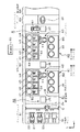
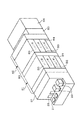
以下、本発明に係る塗布、現像装置の第1の実施の形態について説明する。図1は、本発明の塗布、現像装置をレジストパターン形成装置に適用した場合の一実施の形態の平面図を示し、図2は同概略斜視図、図3は同概略側面図である。この塗布、現像装置は、基板であるウエハWが例えば13枚密閉収納されたキャリア20を搬入出するためのキャリアブロックS1と、ウエハWに対して、塗布処理及び現像処理を行うための処理ブロックS2と、インターフェイスブロックS3と、を備え、露光装置S4に接続されている。
Hereinafter, a first embodiment of a coating and developing apparatus according to the present invention will be described. FIG. 1 shows a plan view of an embodiment in which the coating and developing apparatus of the present invention is applied to a resist pattern forming apparatus, FIG. 2 is a schematic perspective view thereof, and FIG. 3 is a schematic side view thereof. This coating / developing apparatus includes a carrier block S1 for carrying in / out a
前記キャリアブロックS1には、前記キャリア20を複数個載置可能な載置台21と、この載置台21から見て前方の壁面に設けられる開閉部22と、開閉部22を介してキャリア20からウエハWを取り出すためのトランスファーアームCとが設けられている。このトランスファーアームCは、後述する単位ブロックB2の受け渡しステージTRS1,2,3との間でウエハWの受け渡しを行うように、進退自在、昇降自在、鉛直軸回りに回転自在、キャリア20の配列方向に移動自在に構成されている。
In the
キャリアブロックS1の奥側には筐体24にて周囲を囲まれる処理ブロックS2が接続されている。処理ブロックS2は、この例では、キャリアブロックS1側に配置された、各々ウエハWの搬送路がキャリアブロックS1からインターフェイスブロックS3に向かって直線状に伸びる第1の積層ブロック部41と、この第1の積層ブロック部41に対してインターフェイスブロックS3側に配置され、各々ウエハWの搬送路が第1の積層ブロック部41における前記搬送路に対して一直線となるようにインターフェイスブロックS3に向かって伸びる第2の積層ブロック部42とを備えている。
A processing block S2 surrounded by a
第1の積層ブロック部41は、露光後のウエハWに対して現像液を塗布し現像を行うための現像用の単位ブロック(DEV層)B1と、ウエハWに対してレジスト液を塗布するためのレジスト膜用の単位ブロック(COT層)B2と、レジスト液を塗布する前のウエハWに反射防止膜用の薬液を塗布するための底部反射防止膜用の単位ブロック(BCT層)B3と、を下からこの順に積層して構成される。また第2の積層ブロック部42は、露光後のウエハWに対して現像液を塗布し現像を行うための現像用の単位ブロック(DEV層)B4と、レジスト液を塗布した後のウエハWに反射防止膜用の薬液を塗布するための上部反射防止膜用の単位ブロック(TCT層)B5と、ウエハWに対してレジスト液を塗布するためのレジスト膜用の単位ブロック(COT層)B6と、を下からこの順に積層して構成される。以下において、記述の冗長さを回避するために、「単位ブロック」という用語と「○○層」という用語との両方を適宜用いるものとする。前記DEV層B1、COT層B2及びBCT層B3は、夫々DEV層B4、TCT層B5及びCOT層B6と同じ高さ位置に配置されている。
The first
第1の積層ブロック部41と第2の積層ブロック部42との間には、各段の単位ブロックB1〜B3(B4〜B6)に対応する位置、つまり単位ブロックにおける後述のメインアームによりウエハWを受け渡しできる位置に受け渡しステージである中間ステージTRS6、TRS7、TRS8が設けられている。
Between the first
続いて単位ブロックB1〜B6の構成について説明する。これら各単位ブロックB1〜B6は、ウエハWに対して薬液を塗布するための液処理ユニットと、前記液処理ユニットにて行なわれる処理の前処理及び後処理を行なうための各種の加熱・冷却系の処理ユニットと、前記液処理ユニットと加熱・冷却系の処理ユニットとの間でウエハWの受け渡しを行うための単位ブロック用の搬送手段であるメインアームA1〜A6と、を備えている。 Next, the configuration of the unit blocks B1 to B6 will be described. Each of these unit blocks B1 to B6 includes a liquid processing unit for applying a chemical solution to the wafer W, and various heating / cooling systems for performing pre-processing and post-processing of processing performed in the liquid processing unit. And main arms A1 to A6 which are transfer means for unit blocks for transferring the wafer W between the liquid processing unit and the heating / cooling processing unit.
これら単位ブロックB1〜B6は、この例では、各単位ブロックB1〜B6の間で、前記液処理ユニットと、加熱・冷却系の処理ユニットと、搬送手段Aとの配置レイアウトが同じに形成されている。ここで配置レイアウトが同じであるとは、各処理ユニットにおけるウエハWを載置する中心つまり液処理ユニットにおける後述するスピンチャックの中心や、加熱ユニットや冷却ユニットにおける加熱プレートや冷却プレートの中心が同じという意味である。 In this example, these unit blocks B1 to B6 are formed in the same arrangement layout of the liquid processing unit, the heating / cooling processing unit, and the conveying means A between the unit blocks B1 to B6. Yes. Here, the same arrangement layout means that the center on which the wafer W is placed in each processing unit, that is, the center of the spin chuck described later in the liquid processing unit, and the center of the heating plate or cooling plate in the heating unit or cooling unit are the same. It means that.
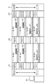
先ず図1に示すCOT層B2を例にして以下に説明する。このCOT層B2のほぼ中央には、COT層B2の長さ方向(図中Y軸方向)に、キャリアブロックS1とインターフェイスブロックS3とを接続するための、ウエハWの搬送領域R1が形成されている。この搬送領域R1のキャリアブロックS1側から見た両側には、手前側(キャリアブロックS1側)から奥側に向かって右側に、前記液処理ユニットとして、レジストの塗布処理を行うための複数個の塗布部を備えた塗布ユニット31が設けられている。またCOT層B2の手前側から奥側に向かって左側には、順に加熱・冷却系のユニットを2段化した4個の棚ユニットU1,U2,U3,U4(2段のユニットを棚ユニットと呼んでいる)が設けられており、塗布ユニット31にて行なわれる処理の前処理及び後処理を行なうための各種ユニットを複数段、例えば2段に積層した構成とされている。こうして前記搬送領域R1は区画されており、例えばこの区画された搬送領域R1に清浄エアを噴出させて排気することにより、当該領域内のパーティクルの浮遊を抑制するようになっている。
First, the COT layer B2 shown in FIG. 1 will be described below as an example. Near the center of the COT layer B2, a transfer region R1 for the wafer W for connecting the carrier block S1 and the interface block S3 is formed in the length direction of the COT layer B2 (Y-axis direction in the figure). Yes. On both sides of the transport region R1 viewed from the carrier block S1 side, a plurality of resist coating processes are performed as the liquid processing unit on the right side from the near side (carrier block S1 side) toward the back side. An
上述の前処理及び後処理を行うための各種ユニットの中には、例えば図4に示すように、レジスト液の塗布前にウエハWを所定の温度に調整するための冷却ユニット(COL2)、レジスト液の塗布後にウエハWの加熱処理を行うための例えばプリベーキングユニットなどと呼ばれている加熱ユニット(CHP2)等が含まれている。また冷却ユニット(COL2)や加熱ユニット(CHP2)等の各処理ユニットは、夫々処理容器51内に収納されており、棚ユニットU1〜U4は、前記処理容器51が2段に積層されて構成され、各処理容器51の搬送領域R1に臨む面にはウエハ搬出入口52が形成されている。なお加熱ユニット(CHP2)とは、図1に示すように、加熱プレート53と、搬送アームを兼用する冷却プレート54とを備えた構成である。更にまた棚ユニットU1〜U4の中には、ウエハWの表面とレジスト膜との密着性を高めるために当該表面に例えば有機系のガスを供給して疎水化処理を行う疎水化ユニット(ADH2)が含まれている。
Among the various units for performing the above pre-processing and post-processing, for example, as shown in FIG. 4, a cooling unit (COL2) for adjusting the wafer W to a predetermined temperature before applying the resist solution, a resist For example, a heating unit (CHP2) called a pre-baking unit or the like for performing the heat treatment of the wafer W after the application of the liquid is included. Each processing unit such as the cooling unit (COL2) and the heating unit (CHP2) is housed in the
前記搬送領域R1には前記メインアームA2が設けられている。このメインアームA2は、当該COT層B2内の全てのモジュール(ウエハWが置かれる場所)、例えば棚ユニットU1〜U4の各処理ユニット、塗布ユニット31、後述する棚ユニットU5及び既述の中間ステージTRS7との間でウエハの受け渡しを行うように構成されており、このために進退自在、昇降自在、鉛直軸回りに回転自在、Y軸方向に移動自在に構成されている。
The main arm A2 is provided in the transfer region R1. The main arm A2 includes all modules (places where the wafer W is placed) in the COT layer B2, such as the processing units of the shelf units U1 to U4, the
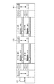
またキャリアブロックS1と第1の積層ブロック部41との間には、図1及び図3に示すように、トランスファーアームCと各単位ブロックB1〜B3のメインアームA1〜A3とがアクセスできる位置に棚ユニットU5が設けられている。より具体的には、前記棚ユニットU5は、図3に示すように、各メインアームA1〜A3との間で夫々ウエハWの受け渡しを行うことができるように、受け渡しステージTRS1〜TRS3を備えており、この例では各単位ブロックB1〜B3に対応して夫々2段づつ受け渡しステージTRS1〜TRS3が設けられている。
Further, as shown in FIGS. 1 and 3, the transfer arm C and the main arms A1 to A3 of the unit blocks B1 to B3 can be accessed between the carrier block S1 and the first
更に第2の積層ブロック部42とインターフェイスブロックS3との間には、図3に示すように棚ユニットU7が設けられ、この棚ユニットU7は、第2の積層ブロック部42の各メインアームA4〜A6との間で夫々ウエハWの受け渡しを行うことができるように、受け渡しステージTRS9〜TRS11を備えており、この例では各単位ブロックB4〜B6に対応して夫々2段づつ受け渡しステージTRS9〜TRS11が設けられている。
Further, a shelf unit U7 is provided between the second
また図1に示すように、処理ブロックS2には受け渡しステージTRS10及びTRS11に対してウエハWの受け渡しを行うことができるように昇降自在、進退自在な搬送手段である受け渡しアーム61が設けられている。この受け渡しアーム61は、後述のようにCOT層B6にてレジスト膜が形成されたウエハWに対してそのうえに更に反射防止膜を形成する場合に、COT層B6から受け渡しステージTRS11に排出されたウエハWをTCT層B5に対応する受け渡しステージTRS10に受け渡す機能を有する。
Further, as shown in FIG. 1, the processing block S2 is provided with a
一方、処理ブロックS2における棚ユニットU6の奥側には、インターフェイスブロックS3を介して露光装置S4が接続されている。インターフェイスブロックS3には、処理ブロックS2の棚ユニットU6と露光装置S4とに対してウエハWの受け渡しを行うためのインターフェイスアーム62を備えている。このインターフェイスアーム62は、処理ブロックS2と露光装置S4との間に介在するウエハWの搬送手段をなすものであり、この例では、棚ユニットU6の受け渡しステージTRS9〜TRS11に対してウエハWの受け渡しを行うように、進退自在、昇降自在、鉛直軸回りに回転自在に構成されている。COT層B6でレジスト膜が塗布されたウエハWに対して更に反射防止膜を形成するために受け渡しステージTRS11からTRS10に当該ウエハWを搬送する動作について、この例ではインターフェイスアーム62の負担を大きくしないように受け渡しアーム61に受け持たせているが、当該受け渡しアーム61を設けずにインターフェイスアーム62に受け持たせるようにしてもよい。
On the other hand, an exposure apparatus S4 is connected to the back side of the shelf unit U6 in the processing block S2 via an interface block S3. The interface block S3 includes an
続いて他の単位ブロックについて簡単に説明する。DEV層B1、B4、BCT層B3、TCT層B5は、COT層B2、B6と同様に構成されており、差異としては、液処理ユニットである塗布ユニット31において、薬液としてレジスト液の代わりに反射防止膜用の薬液あるいは現像用の薬液(現像液)が用いられる点、薬液の塗布の手法が異なる点が挙げられ、また加熱系、冷却系のユニットにおける処理条件が異なる点などが挙げられる。しかしメインアームA1、A3、A4、A5が各処理ユニットに対してウエハWを受け渡し、更に棚ユニットU5あるいはU7の受け渡しステージと棚ユニットU6の中間ステージとの間でウエハWの受け渡しをする点において同様の構成である。また第2の積層ブロック部42におけるTCT層B5及びCOT層B6は、続く露光処理の前にウエハWのエッジ部のみを選択的に露光するために周縁露光装置(WEE)が例えば棚ユニットU4に組み込まれる構成となっている。
Next, other unit blocks will be briefly described. The DEV layers B1, B4, BCT layer B3, and TCT layer B5 are configured in the same manner as the COT layers B2 and B6. The difference is that the
続いて塗布ユニット31について、図5を用いて簡単に説明する。この例では3個の塗布部301,302,303が共通の処理容器300の内部に収納され、夫々が搬送領域R1に臨むように横方向(Y軸方向)に配列した状態で共通のベース304に設けられている。
Next, the
これら塗布部301,302,303は同様に構成されているので、塗布部301を例にして説明すると、図中305は基板保持部をなすスピンチャックであり、真空吸着によりウエハWを水平に保持するように構成されている。このスピンチャック305は駆動部306により鉛直軸回りに回転でき、かつ昇降できるようになっている。またスピンチャック305の周囲にはウエハWからスピンチャック305に跨る側方部分を囲うカップ307が設けられ、当該カップ307の底面には排気管やドレイン管などを含む排液部308が設けられている。図中309は、スピンチャック302に保持されたウエハWの周縁部にリンス液を供給するためのサイドリンス機構であり、昇降自在、鉛直軸回りに回転自在に構成されている。
Since the
また図中310は、3個の塗布部301,302,303に対して塗布液を供給するための共通の供給ノズル(薬液ノズル)であり、この供給ノズル310は移動機構312により、処理容器300の長さ方向(Y方向)に沿って設けられたガイドレール311に沿って、一端側の塗布部301のカップ307の外方側から他端側の塗布部303のカップ307の外方側まで移動自在、かつ昇降自在に構成されている。これによりこの例では供給ノズル310により、各塗布部301〜303のスピンチャック305に保持されたウエハWのほぼ中央領域にレジスト液を供給するようになっている。図中313は、一端側の塗布部301の外側に設けられた供給ノズル310の待機領域である。
In the drawing,
図中314は処理容器300の天井部に取り付けられたフィルタユニット、315は処理容器300の底面に設けられた排気部であり、排気部から所定の排気量で排気すると共に、フィルタユニット317から所定流量の、温度と湿度とが調整された清浄気体を供給することにより、処理容器300内に清浄気体のダウンフローが形成され、メインアームA4の搬送領域R1よりも陽圧になるように設定されている。図中316は、処理容器300の搬送領域R1に臨む面に形成されたウエハWの搬入出口である。
In the figure,
この塗布ユニット31では、ウエハWはメインアームA4により搬入出口316を介して処理容器300内に搬入され、予め決定された塗布部301,302,303のいずれかのスピンチャック305に受け渡される。そして供給ノズル310から当該ウエハWの中央部にレジスト液を供給すると共に、スピンチャック305を回転させ、レジスト液を遠心力によりウエハWの径方向に広げ、ウエハW表面にレジストの液膜を形成させる。こうしてレジストの液膜が形成されたウエハWは搬入出口316を介してメインアームAにより塗布ユニット31の外部に搬出される。
In the
このような塗布ユニット31では、3個の塗布部301〜303が共通の処理容器300の内部に設けられているので処理雰囲気が同じである。このため供給ノズル310を共用化でき、1本の供給ノズル310により3個の塗布部301〜303に対してレジスト液を供給することができるようになっているので、各塗布部301〜303毎に処理容器300と供給ノズル310とを設ける場合に比べて、トータルの部材点数や占有面積を削減できる。
In such a
ここで図1に戻って、この塗布、現像装置は制御部50を備えており、制御部50はウエハWに対して処理ブロックS2における処理モードを指定できるように構成されている。ここでいう処理モードとは、ウエハWが順番に搬送されていくユニットの配列を意味するものであり、処理モードの指定の仕方としては、搬送される順にユニットを入力するようにしてもよいし、またはどの単位ブロックに対してどの順番にウエハWを搬送するかという指定の方法であってもよいし、あるいは種々のウエハWの搬送経路に対応するユニットの配列データと処理種別とを対応づけたデータを作成しておいてこの中から処理種別を選択するようにしてもよい。また使用する単位ブロックを順番に指定し、単位ブロックが指定されると、自動的に各単位ブロック毎に例えばそのときのウエハWの滞留の状況を判断して、使用するユニットを選択する場合であってもよい。 Returning to FIG. 1, the coating and developing apparatus includes a control unit 50, and the control unit 50 is configured to be able to designate a processing mode in the processing block S <b> 2 for the wafer W. The processing mode here means an arrangement of units in which the wafers W are transferred in order. As a method for specifying the processing mode, the units may be input in the order of transfer. Alternatively, it may be a method of specifying in which order the wafer W is transferred to which unit block, or the arrangement data of units corresponding to the transfer paths of various wafers W are associated with the processing types. Alternatively, the processing type may be selected from the generated data. In addition, when the unit blocks to be used are specified in order and the unit blocks are specified, for example, when the unit W is automatically determined for each unit block and the unit to be used is selected. There may be.
処理モードの一例を述べると、
第1の積層ブロック部41のBCT層B3→第2の積層ブロック部42のCOT層B6の経路で搬送される処理モードM1、
第1の積層ブロック部41のCOT層B2→第2の積層ブロック部42のTCT層B5の経路で搬送される処理モードM2、
第1の積層ブロック部41のBCT層B3→第2の積層ブロック部42のCOT層B6→第2の積層ブロック部42のTCT層B5の経路で搬送される処理モードM3、
第1の積層ブロック部41のBCT層B3→第1の積層ブロック部41のCOT層B2→第2の積層ブロック部42のTCT層B5の経路で搬送される処理モードM4、
第1の積層ブロック部41のCOT層B2だけを使用する処理モードM5、
第2の積層ブロック部42のCOT層B6だけを使用する処理モードM6、
などを挙げることができる。なおここで述べた処理モードは、露光前の処理についてだけ記載してあり、各処理モードにおいてウエハWが露光装置S4に搬送され、その後DEV層B4あるいはB1に搬送されて現像されることについては同じである。
次いでこの実施の形態の作用について説明する。先ず制御部50にて前記処理モードM1を選択したとする。先ず外部からキャリア20がキャリアブロック21に搬入され、トランスファーアームCによりこのキャリア20内からウエハWが取り出される。ウエハWは、トランスファーアームCから棚ユニットU5の受け渡しステージTRS3に受け渡され、そして第1の積層ブロック部41におけるBCT層B3のメインアームA3に受け渡される。そしてBCT層B3では、メインアームA3により、冷却ユニット(COL)→反射防止膜形成ユニット(図示していないが、図1における塗布ユニット31に対応するユニットである)→加熱ユニット(CHP)の順序で搬送されて、ウエハW上に第1の反射防止膜が形成される。なおBCT層B3における処理ユニットの配列については図示されていないが、既述のように実質図4と同じ構成であることから、図4を参照することで搬送経路のイメージは把握されるはずである。
An example of processing mode is:
Processing mode M1 transported by the path of the BCT layer B3 of the first
A processing mode M2 transported by a route from the COT layer B2 of the first
A processing mode M3 transported by a route of BCT layer B3 of the first
A processing mode M4 transported by a route of BCT layer B3 of the first
A processing mode M5 using only the COT layer B2 of the first
A processing mode M6 using only the COT layer B6 of the second
And so on. Note that the processing modes described here are only described for pre-exposure processing. In each processing mode, the wafer W is transferred to the exposure apparatus S4 and then transferred to the DEV layer B4 or B1 and developed. The same.
Next, the operation of this embodiment will be described. First, it is assumed that the processing mode M1 is selected by the control unit 50. First, the
続いてこのウエハWはメインアームA3により棚ユニットU6の中間ステージTRS8に受け渡され、更に第2の積層ブロック部42におけるCOT層B6のメインアームA6に受け渡される。そしてCOT層B6では、メインアームA6により、疎水化処理ユニット(ADH)→冷却ユニットCOL→塗布ユニット31→加熱ユニットCHPの順序で搬送されてウエハW上にレジスト膜が形成され、更に周縁露光装置(WEE)に搬送されて周縁部が露光される。その後このウエハWは、メインアームA6により棚ユニットの受け渡しステージTRS11に搬送され、インターフェイスアームDにより露光装置S4に搬送され、ここで所定の露光処理が行われる。図6には、処理モードM1に対応するウエハWの流れが実線の矢印により示されている。
Subsequently, the wafer W is transferred to the intermediate stage TRS8 of the shelf unit U6 by the main arm A3, and further transferred to the main arm A6 of the COT layer B6 in the second
露光処理後のウエハWは、インターフェイスアームDにより、棚ユニットU6の受け渡しステージTRS9に搬送され、更にDEV層B4のメインアームA4に受け取られる。そして例えばDEV層B4にて、先ず加熱ユニット(PEB)→冷却ユニット(COL)→現像ユニット→加熱ユニット(POST)の順序で搬送され、所定の現像処理が行われる。こうして現像処理が行われたウエハWは、棚ユニットU6の中間ステージTRS6を介してDEV層B1のメインアームA1に受け渡され、更に棚ユニットU5の受け渡しステージTRS1を介してトランスファーアームCに受け渡され、キャリアブロックS1に載置されている元のキャリア20に戻される。ウエハWに対する現像処理は、DEV層B4にて行う代わりに当該DEV層B4を通過させてDEV層B1にて行うようにしてもよいが、通常反射防止膜の形成処理及びレジストスト膜の形成処理に比べて現像処理の方が長い時間がかかることから、DEV層B1、B4の両方を用いる場合が多い。
The wafer W after the exposure process is transferred to the transfer stage TRS9 of the shelf unit U6 by the interface arm D, and further received by the main arm A4 of the DEV layer B4. Then, for example, in the DEV layer B4, first, the film is transported in the order of the heating unit (PEB) → the cooling unit (COL) → the developing unit → the heating unit (POST), and a predetermined developing process is performed. The wafer W thus developed is transferred to the main arm A1 of the DEV layer B1 via the intermediate stage TRS6 of the shelf unit U6, and further transferred to the transfer arm C via the transfer stage TRS1 of the shelf unit U5. Then, the
次に処理モードM2を選択したとする。この場合には、キャリア20内のウエハWは、トランスファーアームCにより棚ユニットU5の受け渡しステージTRS2に搬送され、COT層B2のメインアームA2に受け取られ、ここでレジスト膜の形成処理が行われる。次いでこのウエハWは棚ユニットU6の中間ステージTRS7を介してTCT層B5のメインアームA5に受け渡され、BCT層B3にて説明したと同様にしてレジスト膜の上に反射防止膜が形成される。図6には、処理モードM2に対応するウエハWの流れが鎖線の矢印により示されている。しかる後ウエハWは棚ユニットU7の受け渡しステージTRS10に受け渡され、以降は処理モードM1と同様の搬送、処理が行われる。
Next, assume that the processing mode M2 is selected. In this case, the wafer W in the
また処理モードM3が選択された場合には、ウエハWが第1の積層ブロック部41のBCT層B3にて反射防止膜が形成され、続いて棚ユニットU6の中間ステージTRS8を介して第2の積層ブロック部42のCOT層B6に搬送されてレジスト膜が形成されるまでは、処理モードM1と同様であるが、棚ユニットU7の受け渡しステージTRS11に受け渡された後は、専用の受け渡しアーム61にて受け渡しステージTRS10に搬送される。その後TCT層B5のメインアームA5に受け取られ、当該TCT層B5にてウエハW上のレジスト膜の上に反射防止膜が形成される。そしてこのウエハWは棚ユニットU7の受け渡しステージTRS10に搬送され、以降は同様の処理が行われることになる。図6には、処理モードM3に対応するウエハWの流れが点線の矢印により示されている。
When the processing mode M3 is selected, an antireflection film is formed on the wafer W in the BCT layer B3 of the first
なお処理モードM5あるいはM6が選択された場合には、COT層B2あるいはB6が使用されて、ウエハW上にレジスト膜だけが形成されて露光装置S4に搬送されることになる。 When the processing mode M5 or M6 is selected, the COT layer B2 or B6 is used, and only the resist film is formed on the wafer W and transferred to the exposure apparatus S4.
上述の実施の形態によれば、液処理を行うためのユニット及びそれらユニット間の搬送を行う搬送手段をブロック化して単位ブロックとし、露光前の塗布処理を行う単位ブロック(COT層B2、B6及びBCT層B3並びにTCT層B5)と、露光後の現像処理を行う単位ブロック(DEV層B1、B4)と、を上下に分離すると共に、露光前の塗布処理を行うユニットを第1の積層ブロック部41と第2の積層ブロック部42とに前後に分散し、更に反射防止膜をレジスト膜の上に塗布するのか下に塗布するのかあるいは上下に塗布するのかによって、両積層ブロック部への搬送の仕方を変えている。従って、処理部である処理ブロックS2において露光前の基板の搬送と露光後の基板の搬送とを別々の搬送手段により行うため、搬送効率が高いし、更に塗布処理を行う単位ブロックを単純に積層する場合に比べて装置の高さを抑えることができるのでメンテナンスが行いやすく、また塗布処理を行う単位ブロックを1層により構成した場合に比べて単位ブロックの長さを抑えることができるので、設置面積の増大を阻むことができる。
According to the above-described embodiment, the unit for performing liquid processing and the transport means for transporting between the units are blocked to form unit blocks, and the unit blocks (COT layers B2, B6 and BCT layer B3 and TCT layer B5) and unit blocks (DEV layers B1, B4) for performing development processing after exposure are separated vertically, and a unit for performing coating processing before exposure is a first laminated block section. 41 and the second
そして棚ユニットU6の中間ステージTRS7またはTRS8を介して両積層ブロック部41、42の互いに対応する高さの単位ブロック間(B3、B6間あるいはB2、B5間)の基板の搬送を行うようにしているため、各単位ブロックの搬送手段を利用して基板の搬送を行うことができるので、両積層ブロック部41、42間の基板受け渡し専用の搬送手段を設けなくて済み、搬送系の構成が簡単になる。なお各中間ステージTRS7またはTRS8は、単位ブロック間(B3、B6間あるいはB2、B5間)のスループットを合わせるために、複数台設けるようにしてもよい。
Then, the substrate is transported between the unit blocks having the corresponding heights of the
図7には、本発明の他の実施の形態に係る要部が示されている。この例は、露光装置S4として、ウエハWの表面に液層を形成して液浸露光を行なう装置を用い、露光前のウエハWの表面に対して撥水性の保護膜を形成するためのユニットを有する単位ブロック(DCT層)B7を第1の積層ブロック部41及び第2の積層ブロック部42の一方に設ける例である。前記撥水性の保護膜を形成するためのユニットとは、液浸露光される際の液体がレジストに含浸されるのを防ぐための保護膜を塗布する撥水性保護膜塗布ユニットであり、またこの単位ブロックB7には露光後の保護膜の除去や露光前後にウエハWに付着したパーティクルや、露光に支障をきたす成分を除去洗浄するための洗浄ユニットが設けられても良い。
FIG. 7 shows a main part according to another embodiment of the present invention. In this example, a unit for forming a water-repellent protective film on the surface of the wafer W before exposure using an apparatus that performs immersion exposure by forming a liquid layer on the surface of the wafer W as the exposure apparatus S4. This is an example in which a unit block (DCT layer) B <b> 7 having s is provided on one of the first
この場合、棚ユニットU7の受け渡しステージTRS10あるいはTRS11から排出されたウエハWは、受け渡しアーム62により受け渡しステージTRS12に搬送され、その後DCT層B7のメインアームB7に受け渡されて、当該DCT層B7にて上記の保護膜が形成され、受け渡しステージTRS12を介してインターフェイスアームDに受け渡されることになる。
In this case, the wafer W discharged from the transfer stage TRS10 or TRS11 of the shelf unit U7 is transferred to the transfer stage TRS12 by the
更にまた本発明は、図8及び図9に示すように第1の積層ブロック部41と第2の積層ブロック部42との間に、先の実施の形態にて用いた受け渡しアーム62の代わりの役割を果たす受け渡しアーム63を設けてもよい。この場合、例えばこれら積層ブロック41、42の最上段の単位ブロックに対応する高さ位置と最下段の単位ブロックに対応する高さ位置との間で昇降できる搬送手段である受け渡しアーム63を設けてもよい。この例では、受け渡しアーム63により第2の積層ブロック部42の単位ブロック間(例えばCOT層B6及びTCT層b5間)の搬送を実現するにあたり、棚ユニットU6を利用している。このため各単位ブロック毎の中間ステージTRS、即ち中間ステージTRS6〜TRS8を2段化している。
Furthermore, in the present invention, as shown in FIG. 8 and FIG. 9, a replacement of the
またこのような図8に示す例の変形例を図10に示しておくと、この例では、第1の積層ブロック部41はDEV層B1及びBCT層B3の積層体からなり、第2の積層ブロック部42は、TCT層B5及びCOT層B6の積層体からなる。
In addition, if a modification of the example shown in FIG. 8 is shown in FIG. 10, in this example, the first
以上において、第2の積層ブロック部42の一段目の単位ブロックは、DEV層B4として構成する代わりに、検査用の単位ブロックとして構成してもよいし、あるいは、液浸露光を行う場合には露光後の保護膜の除去や露光前後にウエハWに付着したパーティクルや、露光に支障をきたす成分を除去洗浄するための洗浄ユニットが設けられても良い。
In the above, the first unit block of the second
この単位ブロックを検査用の単位ブロックとして構成する場合、当該単位ブロックは、検査用のユニットとユニットに対してウエハWの受け渡しを行うことができるメインアームとを備えた構成であり、既述の単位ブロックにおいて、液処理ユニットや熱系のユニットの代わりに検査ユニットが配置された構成である。塗布膜形成後露光処理前に行う検査としては、塗布膜の膜厚の検査や異物検査等があり、露光処理後現像処理前に行う検査としては、露光重ね合わせ検査等がある。またこれらに限らず、基板上のアライメントマークを検出するユニットや、レーザー処理により膜を一部除去するユニットを設けるようにしてもよい。 When this unit block is configured as a unit block for inspection, the unit block includes a unit for inspection and a main arm that can deliver the wafer W to the unit. In the unit block, an inspection unit is arranged instead of the liquid processing unit and the thermal system unit. Examples of the inspection performed after the coating film formation and before the exposure process include an inspection of the film thickness of the coating film and a foreign matter inspection. Examples of the inspection performed after the exposure process and before the development processing include an exposure overlay inspection. Further, the present invention is not limited thereto, and a unit for detecting an alignment mark on the substrate and a unit for removing a part of the film by laser processing may be provided.
そして前記補助ブロックに設けられるユニットとしては、ウエハ表面の状態を検査するための、例えばウエハWに形成された塗布膜の膜厚を検査するための膜厚検査ユニット、レジスト液の塗布ムラを検出するための塗布ムラ検出装置、露光前及び/又は露光後の基板を洗浄するための洗浄ユニット、露光装置にて生じるパターンの位置ずれを検出するためのデフォーカス検査装置、現像処理の不良を検出するための現像不良検出装置、ウエハWに付着したパーティクル数を検出するためのパーティクル数検出装置、レジスト塗布後のウエハW表面にレジスト液中の気泡や異物によって発生するコメットを検出するためのコメット検出装置、ウエハW表面から飛び出したレジスト液の溶剤がウエハWに再付着するスプラッシュバックを検出するスプラッシュバック検出装置、ウエハW表面の同一場所に同一の形状で現れる共通欠陥を検出する共通欠陥検出装置、現像処理後のウエハWに残存するレジスト残渣を検出するためのスカム検出装置、レジスト塗布処理及び/又は現像処理がされていない不具合を検出するためのNO RESIST,NO DEVELOP検査装置(不具合検出装置)、ウエハW上に形成されたレジスト膜の線幅を測定するための線幅測定装置、露光装置にて露光されたウエハWとフォトマスクとの重ね合わせ精度を規格値と比較して検査するための重ね合わせ検査装置の少なくとも一つが設けられる。 As the unit provided in the auxiliary block, for example, a film thickness inspection unit for inspecting the state of the wafer surface, for example, inspecting the film thickness of the coating film formed on the wafer W, and detecting coating unevenness of the resist solution Coating unevenness detection device for cleaning, cleaning unit for cleaning a substrate before and / or after exposure, a defocus inspection device for detecting a positional deviation of a pattern generated in the exposure device, and a defect in development processing are detected Development defect detection device for detecting the number of particles adhering to the wafer W, and a comet for detecting comets generated by bubbles or foreign substances in the resist solution on the surface of the wafer W after resist coating Detection device detects splash back in which solvent of resist solution jumping out from wafer W surface reattaches to wafer W Splash back detection apparatus, common defect detection apparatus for detecting common defects appearing in the same shape at the same location on the surface of the wafer W, scum detection apparatus for detecting resist residue remaining on the wafer W after development processing, resist coating process And / or a NO RESIST, NO DEVELOP inspection apparatus (defect detection apparatus) for detecting defects that are not developed, a line width measuring apparatus for measuring the line width of the resist film formed on the wafer W, At least one overlay inspection apparatus for inspecting the overlay accuracy of the wafer W exposed by the exposure apparatus and the photomask by comparing with a standard value is provided.
なお本発明は半導体ウエハのみならず液晶ディスプレイ用のガラス基板(LCD基板)といった基板を処理する塗布、現像装置にも適用できる。 The present invention can be applied to a coating and developing apparatus for processing not only a semiconductor wafer but also a substrate such as a glass substrate (LCD substrate) for a liquid crystal display.
W 半導体ウエハ
20 キャリア
C トランファーアーム
S1 キャリアブロック
S2 処理ブロック
S3 インターフェイスブロック
S4 露光装置
A1〜A7 メインアーム
31 塗布ユニット
41 第1の積層ブロック部
42 第2の積層ブロック部
TRS6〜TRS8 中間ステージ
61 受け渡しアーム
62 インターフェイスアーム
50 制御部
B1〜B7 単位ブロック
Claims (4)
a)前記処理部は、キャリアブロック側に配置された、各々基板の搬送路がキャリアブロックからインターフェイスブロックに向かって伸びると共に互いに積層された複数の単位ブロックからなる第1の積層ブロック部と、この第1の積層ブロック部に対してインターフェイスブロック側に配置され、各々基板の搬送路が前記第1の積層ブロック部からインターフェイスブロックに向かって伸びると共に互いに積層された複数の単位ブロックからなる第2の積層ブロック部と、第1の積層ブロック部と第2の積層ブロック部との間において単位ブロックの各段毎に設けられ、両積層ブロック部の間で基板を受け渡すための中間ステージと、を備え、
b)第1の積層ブロック部は、レジスト液を塗布する前の基板に反射防止膜用の薬液を塗布するための底部反射防止膜用の単位ブロックと、基板にレジスト液を塗布するためのレジスト膜用の単位ブロックと、露光後の基板に対して現像液を塗布し現像を行うための現像用の単位ブロックと、を備え、
c)第2の積層ブロック部は、第1の積層ブロック部の底部反射防止膜用の単位ブロックに対応する高さ位置に設けられ、基板にレジスト液を塗布するためのレジスト膜用の単位ブロックと、第1の積層ブロック部のレジスト膜用の単位ブロックに対応する高さ位置に設けられ、レジスト液を塗布した後の基板に反射防止膜用の薬液を塗布するための上部反射防止膜用の単位ブロックと、第1の積層ブロック部の現像用の単位ブロックに対応する高さ位置に設けられ、露光後の基板に対して現像液を塗布し現像を行うための現像用の単位ブロックと、を備え、
d)前記各単位ブロックは、薬液を基板に塗布するための液処理ユニットと、基板を加熱する加熱ユニットと、基板を冷却する冷却ユニットと、これらユニット間で基板を搬送する単位ブロック用の搬送手段と、を備え、
e)基板に対して露光前に行う処理のモードとして、複数の処理モードの中から一つの処理モードを指定するための制御部を設け、前記複数の処理モードは、第1の積層ブロック部における底部反射防止膜用の単位ブロックにて反射防止膜が形成された基板を、当該単位ブロックに対応する中間ステージを介して第2の積層ブロック部におけるレジスト膜用の単位ブロックに搬送し、当該基板に対してレジスト膜を形成する工程を含む処理モードと、第1の積層ブロック部におけるレジスト膜用の単位ブロックにてレジスト膜が形成された基板を、当該単位ブロックに対応する中間ステージを介して第2の積層ブロック部における上部反射防止膜用の単位ブロックに搬送し、当該基板に対して上部反射防止膜を形成する工程を含む処理モードと、を含むことを特徴とする塗布、現像装置。 The substrate carried into the carrier block by the carrier is transferred to the processing unit, and after the coating film including the resist film is formed in the processing unit, the substrate is transported to the exposure apparatus through the interface block and returned through the interface block. In the coating and developing apparatus for developing the exposed substrate in the processing unit and delivering it to the carrier block,
a) The processing unit is arranged on the carrier block side, each substrate transport path extending from the carrier block toward the interface block and a plurality of unit blocks stacked on each other, The second laminated block is disposed on the interface block side with respect to the first laminated block portion, and each of the substrate transport paths extends from the first laminated block portion toward the interface block and is composed of a plurality of unit blocks stacked on each other. An intermediate stage provided for each stage of the unit block between the laminated block part and the first laminated block part and the second laminated block part, and for transferring the substrate between the laminated block parts; Prepared,
b) The first laminated block portion includes a unit block for the bottom antireflection film for applying the chemical solution for the antireflection film to the substrate before applying the resist solution, and a resist for applying the resist solution to the substrate. A unit block for film, and a unit block for development for applying and developing a developer to the substrate after exposure,
c) The second laminated block portion is provided at a height position corresponding to the unit block for the bottom antireflection film of the first laminated block portion, and a unit block for the resist film for applying a resist solution to the substrate And an upper antireflection film for applying a chemical solution for the antireflection film to the substrate after the resist solution is applied, which is provided at a height position corresponding to the unit block for the resist film of the first laminated block portion And a unit block for development that is provided at a height position corresponding to the unit block for development of the first laminated block portion and that applies a developer to the substrate after exposure and performs development. With
d) Each unit block includes a liquid processing unit for applying a chemical solution to the substrate, a heating unit for heating the substrate, a cooling unit for cooling the substrate, and transport for the unit block for transporting the substrate between these units. Means, and
e) A control unit for designating one processing mode from a plurality of processing modes is provided as a processing mode to be performed on the substrate before exposure, and the plurality of processing modes are set in the first stacked block unit. The substrate on which the antireflection film is formed in the unit block for the bottom antireflection film is transported to the unit block for the resist film in the second stacked block portion via the intermediate stage corresponding to the unit block, and the substrate And a substrate having a resist film formed in a unit block for the resist film in the first laminated block portion through an intermediate stage corresponding to the unit block. A processing mode including the step of transporting to the unit block for the upper antireflection film in the second laminated block portion and forming the upper antireflection film on the substrate , Characterized in that it comprises a coating and developing apparatus.
前記複数の処理モードは、第1の積層ブロック部における底部反射防止膜用の単位ブロックにて反射防止膜が形成された基板を、当該単位ブロックに対応する中間ステージを介して第2の積層ブロック部におけるレジスト膜用の単位ブロックに搬送し、当該基板に対してレジスト膜を形成すると共に、当該基板を第2の積層ブロック部における上部反射防止膜用の単位ブロックに搬送し、当該基板に対して上部反射防止膜を形成する工程を含む処理モードを備えたことを特徴とする請求項1記載の塗布、現像装置。 A transport means that can be moved up and down for transferring the substrate between the unit block for the resist film and the unit block for the upper antireflection film in the second laminated block portion;
In the plurality of processing modes, the substrate on which the antireflection film is formed in the unit block for the bottom antireflection film in the first laminated block portion is transferred to the second laminated block via the intermediate stage corresponding to the unit block. The resist film is transported to the unit block for the resist film in the portion, and the resist film is formed on the substrate, and the substrate is transported to the unit block for the upper antireflection film in the second laminated block portion, The coating and developing apparatus according to claim 1, further comprising a processing mode including a step of forming an upper antireflection film.
前記複数の処理モードは、第1の積層ブロック部における底部反射防止膜用の単位ブロックにて反射防止膜が形成された基板を、第1の積層ブロック部におけるレジスト膜用の単位ブロックに搬送して当該基板に対してレジスト膜を形成し、更に当該レジスト膜用の単位ブロックに対応する中間ステージを介して第2の積層ブロック部における上部反射防止膜用の単位ブロックに搬送し、当該基板に対して上部反射防止膜を形成する工程を含む処理モードを備えたことを特徴とする請求項1記載の塗布、現像装置。 A transport unit capable of moving up and down for transferring the substrate between the unit block for the bottom antireflection film and the unit block for the resist film in the first laminated block unit;
In the plurality of processing modes, the substrate on which the antireflection film is formed in the unit block for the bottom antireflection film in the first laminated block portion is transported to the unit block for the resist film in the first laminated block portion. Then, a resist film is formed on the substrate, and further conveyed to the unit block for the upper antireflection film in the second laminated block portion through an intermediate stage corresponding to the unit block for the resist film, The coating and developing apparatus according to claim 1, further comprising a processing mode including a step of forming an upper antireflection film.
Priority Applications (9)
| Application Number | Priority Date | Filing Date | Title |
|---|---|---|---|
| JP2005025509A JP4459831B2 (en) | 2005-02-01 | 2005-02-01 | Coating and developing equipment |
| TW095103331A TW200710940A (en) | 2005-02-01 | 2006-01-27 | Coating and developing apparatus |
| CNB2006100047910A CN100538519C (en) | 2005-02-01 | 2006-01-28 | Coating developing device |
| US11/342,616 US7793609B2 (en) | 2005-02-01 | 2006-01-31 | Coating and developing apparatus |
| KR1020060009384A KR101075733B1 (en) | 2005-02-01 | 2006-01-31 | Coating and developing system |
| US12/855,524 US20100326353A1 (en) | 2005-02-01 | 2010-08-12 | Coating and developing apparatus |
| US12/855,534 US8302556B2 (en) | 2005-02-01 | 2010-08-12 | Coating and developing apparatus |
| KR1020110014021A KR101125340B1 (en) | 2005-02-01 | 2011-02-17 | Coating and developing system |
| KR1020110014015A KR101188081B1 (en) | 2005-02-01 | 2011-02-17 | Coating and developing system |
Applications Claiming Priority (1)
| Application Number | Priority Date | Filing Date | Title |
|---|---|---|---|
| JP2005025509A JP4459831B2 (en) | 2005-02-01 | 2005-02-01 | Coating and developing equipment |
Related Child Applications (2)
| Application Number | Title | Priority Date | Filing Date |
|---|---|---|---|
| JP2009211737A Division JP2010034566A (en) | 2009-09-14 | 2009-09-14 | Coating and developing apparatus |
| JP2009211791A Division JP2010041059A (en) | 2009-09-14 | 2009-09-14 | Coating and developing apparatus |
Publications (2)
| Publication Number | Publication Date |
|---|---|
| JP2006216614A JP2006216614A (en) | 2006-08-17 |
| JP4459831B2 true JP4459831B2 (en) | 2010-04-28 |
Family
ID=36907616
Family Applications (1)
| Application Number | Title | Priority Date | Filing Date |
|---|---|---|---|
| JP2005025509A Active JP4459831B2 (en) | 2005-02-01 | 2005-02-01 | Coating and developing equipment |
Country Status (5)
| Country | Link |
|---|---|
| US (3) | US7793609B2 (en) |
| JP (1) | JP4459831B2 (en) |
| KR (3) | KR101075733B1 (en) |
| CN (1) | CN100538519C (en) |
| TW (1) | TW200710940A (en) |
Families Citing this family (39)
| Publication number | Priority date | Publication date | Assignee | Title |
|---|---|---|---|---|
| JP4459831B2 (en) * | 2005-02-01 | 2010-04-28 | 東京エレクトロン株式会社 | Coating and developing equipment |
| JP4830523B2 (en) * | 2006-02-08 | 2011-12-07 | 東京エレクトロン株式会社 | Coating, developing apparatus, coating, developing method and computer program for carrying out the method. |
| US20070258712A1 (en) * | 2006-05-03 | 2007-11-08 | Moffat William A | Method and apparatus for the vaporous development of photoresist |
| JP2008072016A (en) * | 2006-09-15 | 2008-03-27 | Tokyo Electron Ltd | Liquid-treating apparatus, liquid-treating method, and storage medium |
| JP4999415B2 (en) * | 2006-09-29 | 2012-08-15 | 東京エレクトロン株式会社 | Substrate processing apparatus, substrate processing method, power supply apparatus for substrate processing apparatus, and power supply method for substrate processing apparatus |
| CN101206992B (en) * | 2006-12-20 | 2010-05-12 | 沈阳芯源微电子设备有限公司 | Even glue developing process capable of economizing time and equipment improved structure |
| JP4687682B2 (en) * | 2007-03-30 | 2011-05-25 | 東京エレクトロン株式会社 | Coating and developing apparatus and method, and storage medium |
| JP2008258208A (en) * | 2007-03-30 | 2008-10-23 | Tokyo Electron Ltd | Coating and developing system and method thereof, and storage medium |
| KR100897850B1 (en) * | 2007-06-18 | 2009-05-15 | 세메스 주식회사 | Apparatus for processing a substrate |
| JP5006122B2 (en) | 2007-06-29 | 2012-08-22 | 株式会社Sokudo | Substrate processing equipment |
| JP4957426B2 (en) * | 2007-07-19 | 2012-06-20 | 東京エレクトロン株式会社 | Coating, developing device, coating, developing device operating method, and storage medium |
| TW200919117A (en) * | 2007-08-28 | 2009-05-01 | Tokyo Electron Ltd | Coating-developing apparatus, coating-developing method and storage medium |
| JP2009135169A (en) * | 2007-11-29 | 2009-06-18 | Tokyo Electron Ltd | Substrate processing system, and substrate processing method |
| JP5160204B2 (en) * | 2007-11-30 | 2013-03-13 | 株式会社Sokudo | Substrate processing equipment |
| JP5318403B2 (en) | 2007-11-30 | 2013-10-16 | 株式会社Sokudo | Substrate processing equipment |
| JP5128918B2 (en) | 2007-11-30 | 2013-01-23 | 株式会社Sokudo | Substrate processing equipment |
| JP5001828B2 (en) * | 2007-12-28 | 2012-08-15 | 株式会社Sokudo | Substrate processing equipment |
| JP5179170B2 (en) | 2007-12-28 | 2013-04-10 | 株式会社Sokudo | Substrate processing equipment |
| JP2010182906A (en) * | 2009-02-06 | 2010-08-19 | Tokyo Electron Ltd | Substrate treatment apparatus |
| JP5462506B2 (en) | 2009-03-18 | 2014-04-02 | 株式会社Sokudo | Substrate processing equipment |
| JP5397399B2 (en) * | 2010-07-09 | 2014-01-22 | 東京エレクトロン株式会社 | Coating and developing equipment |
| JP5408059B2 (en) | 2010-07-09 | 2014-02-05 | 東京エレクトロン株式会社 | Coating, developing device, coating, developing method and storage medium |
| JP5223897B2 (en) | 2010-09-02 | 2013-06-26 | 東京エレクトロン株式会社 | Coating, developing device, coating, developing method and storage medium |
| JP5212443B2 (en) * | 2010-09-13 | 2013-06-19 | 東京エレクトロン株式会社 | Coating, developing device, coating, developing method and storage medium |
| JP5608148B2 (en) * | 2011-11-25 | 2014-10-15 | 株式会社Screenセミコンダクターソリューションズ | Substrate processing equipment |
| JP2013247197A (en) * | 2012-05-24 | 2013-12-09 | Sokudo Co Ltd | Substrate processing device |
| JP5442890B2 (en) * | 2013-05-17 | 2014-03-12 | 株式会社Sokudo | Substrate processing equipment |
| JP5442889B2 (en) * | 2013-05-17 | 2014-03-12 | 株式会社Sokudo | Substrate processing equipment |
| JP6243784B2 (en) | 2014-03-31 | 2017-12-06 | 株式会社Screenセミコンダクターソリューションズ | Substrate processing equipment |
| JP5852219B2 (en) * | 2014-12-24 | 2016-02-03 | 株式会社Screenセミコンダクターソリューションズ | Substrate processing method and substrate processing apparatus |
| CN106610568A (en) * | 2015-10-27 | 2017-05-03 | 沈阳芯源微电子设备有限公司 | Glue coating development process module and control method for module internal environment parameters |
| JP6195601B2 (en) * | 2015-12-03 | 2017-09-13 | 株式会社Screenセミコンダクターソリューションズ | Substrate processing method and substrate processing apparatus |
| JP6439766B2 (en) * | 2016-09-23 | 2018-12-19 | 東京エレクトロン株式会社 | Coating and developing method and coating and developing apparatus |
| JP7195841B2 (en) * | 2018-09-21 | 2022-12-26 | 株式会社Screenホールディングス | Substrate processing equipment |
| JP7186605B2 (en) * | 2018-12-27 | 2022-12-09 | 東京エレクトロン株式会社 | SUBSTRATE PROCESSING APPARATUS AND SUBSTRATE PROCESSING METHOD |
| JP7221048B2 (en) | 2018-12-28 | 2023-02-13 | 株式会社Screenホールディングス | SUBSTRATE PROCESSING APPARATUS AND SUBSTRATE TRANSFER METHOD |
| JP7181081B2 (en) * | 2018-12-28 | 2022-11-30 | 株式会社Screenホールディングス | SUBSTRATE PROCESSING APPARATUS AND SUBSTRATE TRANSFER METHOD |
| JP7297650B2 (en) * | 2019-11-27 | 2023-06-26 | 株式会社Screenホールディングス | SUBSTRATE PROCESSING APPARATUS AND SUBSTRATE TRANSFER METHOD |
| JP2022104056A (en) * | 2020-12-28 | 2022-07-08 | 東京エレクトロン株式会社 | Transport device |
Family Cites Families (20)
| Publication number | Priority date | Publication date | Assignee | Title |
|---|---|---|---|---|
| JP2931820B2 (en) | 1991-11-05 | 1999-08-09 | 東京エレクトロン株式会社 | Plate-like processing apparatus and transport apparatus |
| JP3734095B2 (en) * | 1994-09-12 | 2006-01-11 | 株式会社ニコン | Substrate processing equipment |
| JP3779393B2 (en) * | 1996-09-06 | 2006-05-24 | 東京エレクトロン株式会社 | Processing system |
| JP3851751B2 (en) * | 1999-03-24 | 2006-11-29 | 東京エレクトロン株式会社 | Processing system |
| JP3445757B2 (en) * | 1999-05-06 | 2003-09-08 | 東京エレクトロン株式会社 | Substrate processing apparatus and substrate processing method |
| JP3914690B2 (en) * | 1999-06-30 | 2007-05-16 | 東京エレクトロン株式会社 | Substrate delivery device and coating / developing system |
| US6402400B1 (en) * | 1999-10-06 | 2002-06-11 | Tokyo Electron Limited | Substrate processing apparatus |
| US6402401B1 (en) * | 1999-10-19 | 2002-06-11 | Tokyo Electron Limited | Substrate processing apparatus and substrate processing method |
| KR100348938B1 (en) | 1999-12-06 | 2002-08-14 | 한국디엔에스 주식회사 | Semiconductor manufacturing apparatus for photolithography process |
| TW594835B (en) | 2000-05-09 | 2004-06-21 | Tokyo Electron Ltd | System for coating and developing |
| JP4104828B2 (en) | 2001-02-22 | 2008-06-18 | 東京エレクトロン株式会社 | Processing equipment |
| US6402200B1 (en) * | 2001-04-11 | 2002-06-11 | Raymond T. Myers | Apparatus and method for moving mud flaps to a protected position |
| JP4342147B2 (en) | 2002-05-01 | 2009-10-14 | 大日本スクリーン製造株式会社 | Substrate processing equipment |
| JP2004015023A (en) | 2002-06-11 | 2004-01-15 | Dainippon Screen Mfg Co Ltd | Substrate handling device and handling method |
| KR100974141B1 (en) * | 2002-11-28 | 2010-08-04 | 도쿄엘렉트론가부시키가이샤 | Wafer processing apparatus |
| JP4087328B2 (en) | 2002-11-28 | 2008-05-21 | 東京エレクトロン株式会社 | Coating and developing apparatus and operating method of coating and developing apparatus |
| JP2004266283A (en) | 2004-03-15 | 2004-09-24 | Tokyo Electron Ltd | Equipment for processing substrate |
| JP4955976B2 (en) * | 2005-01-21 | 2012-06-20 | 東京エレクトロン株式会社 | Coating and developing apparatus and method thereof |
| JP4955977B2 (en) * | 2005-01-21 | 2012-06-20 | 東京エレクトロン株式会社 | Coating and developing apparatus and method thereof |
| JP4459831B2 (en) * | 2005-02-01 | 2010-04-28 | 東京エレクトロン株式会社 | Coating and developing equipment |
-
2005
- 2005-02-01 JP JP2005025509A patent/JP4459831B2/en active Active
-
2006
- 2006-01-27 TW TW095103331A patent/TW200710940A/en not_active IP Right Cessation
- 2006-01-28 CN CNB2006100047910A patent/CN100538519C/en not_active Expired - Fee Related
- 2006-01-31 KR KR1020060009384A patent/KR101075733B1/en active IP Right Grant
- 2006-01-31 US US11/342,616 patent/US7793609B2/en active Active
-
2010
- 2010-08-12 US US12/855,524 patent/US20100326353A1/en not_active Abandoned
- 2010-08-12 US US12/855,534 patent/US8302556B2/en active Active
-
2011
- 2011-02-17 KR KR1020110014015A patent/KR101188081B1/en active IP Right Grant
- 2011-02-17 KR KR1020110014021A patent/KR101125340B1/en active IP Right Grant
Also Published As
| Publication number | Publication date |
|---|---|
| US8302556B2 (en) | 2012-11-06 |
| KR20110036019A (en) | 2011-04-06 |
| US20070056514A1 (en) | 2007-03-15 |
| US7793609B2 (en) | 2010-09-14 |
| KR20110033160A (en) | 2011-03-30 |
| CN1815368A (en) | 2006-08-09 |
| TWI299181B (en) | 2008-07-21 |
| US20100300353A1 (en) | 2010-12-02 |
| KR101188081B1 (en) | 2012-10-05 |
| KR101075733B1 (en) | 2011-10-21 |
| KR20060088495A (en) | 2006-08-04 |
| TW200710940A (en) | 2007-03-16 |
| US20100326353A1 (en) | 2010-12-30 |
| JP2006216614A (en) | 2006-08-17 |
| CN100538519C (en) | 2009-09-09 |
| KR101125340B1 (en) | 2012-03-28 |
Similar Documents
| Publication | Publication Date | Title |
|---|---|---|
| JP4459831B2 (en) | Coating and developing equipment | |
| JP5378449B2 (en) | Coating and developing equipment | |
| JP4566035B2 (en) | Coating and developing apparatus and method thereof | |
| JP4955976B2 (en) | Coating and developing apparatus and method thereof | |
| JP4955977B2 (en) | Coating and developing apparatus and method thereof | |
| JP4685584B2 (en) | Coating and developing equipment | |
| JP4985728B2 (en) | Coating and developing apparatus and method thereof | |
| KR101692679B1 (en) | Coating and developing apparatus | |
| JP4414921B2 (en) | Coating and developing apparatus and coating and developing method | |
| JP4716362B2 (en) | Substrate processing system and substrate processing method | |
| JP4877075B2 (en) | Coating, developing device, coating, developing device operating method, and storage medium | |
| WO2006006364A1 (en) | Substrate recovery method and substrate processing apparatus | |
| JP2005175209A (en) | Substrate processing apparatus | |
| JP2010041059A (en) | Coating and developing apparatus | |
| JP2010034566A (en) | Coating and developing apparatus | |
| JP5183994B2 (en) | Substrate processing equipment |
Legal Events
| Date | Code | Title | Description |
|---|---|---|---|
| A621 | Written request for application examination |
Free format text: JAPANESE INTERMEDIATE CODE: A621 Effective date: 20061012 |
|
| A131 | Notification of reasons for refusal |
Free format text: JAPANESE INTERMEDIATE CODE: A131 Effective date: 20090714 |
|
| A521 | Request for written amendment filed |
Free format text: JAPANESE INTERMEDIATE CODE: A523 Effective date: 20090914 |
|
| TRDD | Decision of grant or rejection written | ||
| A01 | Written decision to grant a patent or to grant a registration (utility model) |
Free format text: JAPANESE INTERMEDIATE CODE: A01 Effective date: 20100126 |
|
| A01 | Written decision to grant a patent or to grant a registration (utility model) |
Free format text: JAPANESE INTERMEDIATE CODE: A01 |
|
| A61 | First payment of annual fees (during grant procedure) |
Free format text: JAPANESE INTERMEDIATE CODE: A61 Effective date: 20100210 |
|
| R150 | Certificate of patent or registration of utility model |
Free format text: JAPANESE INTERMEDIATE CODE: R150 Ref document number: 4459831 Country of ref document: JP Free format text: JAPANESE INTERMEDIATE CODE: R150 |
|
| FPAY | Renewal fee payment (event date is renewal date of database) |
Free format text: PAYMENT UNTIL: 20130219 Year of fee payment: 3 |
|
| FPAY | Renewal fee payment (event date is renewal date of database) |
Free format text: PAYMENT UNTIL: 20160219 Year of fee payment: 6 |
|
| R250 | Receipt of annual fees |
Free format text: JAPANESE INTERMEDIATE CODE: R250 |
|
| R250 | Receipt of annual fees |
Free format text: JAPANESE INTERMEDIATE CODE: R250 |
|
| R250 | Receipt of annual fees |
Free format text: JAPANESE INTERMEDIATE CODE: R250 |
|
| R250 | Receipt of annual fees |
Free format text: JAPANESE INTERMEDIATE CODE: R250 |
|
| R250 | Receipt of annual fees |
Free format text: JAPANESE INTERMEDIATE CODE: R250 |
|
| R250 | Receipt of annual fees |
Free format text: JAPANESE INTERMEDIATE CODE: R250 |
|
| R250 | Receipt of annual fees |
Free format text: JAPANESE INTERMEDIATE CODE: R250 |
|
| R250 | Receipt of annual fees |
Free format text: JAPANESE INTERMEDIATE CODE: R250 |