JP5841389B2 - Substrate processing apparatus and substrate processing method - Google Patents
Substrate processing apparatus and substrate processing method Download PDFInfo
- Publication number
- JP5841389B2 JP5841389B2 JP2011215458A JP2011215458A JP5841389B2 JP 5841389 B2 JP5841389 B2 JP 5841389B2 JP 2011215458 A JP2011215458 A JP 2011215458A JP 2011215458 A JP2011215458 A JP 2011215458A JP 5841389 B2 JP5841389 B2 JP 5841389B2
- Authority
- JP
- Japan
- Prior art keywords
- substrate
- unit
- processing
- film
- liquid
- Prior art date
- Legal status (The legal status is an assumption and is not a legal conclusion. Google has not performed a legal analysis and makes no representation as to the accuracy of the status listed.)
- Active
Links
Images


Classifications
-
- H—ELECTRICITY
- H01—ELECTRIC ELEMENTS
- H01L—SEMICONDUCTOR DEVICES NOT COVERED BY CLASS H10
- H01L21/00—Processes or apparatus adapted for the manufacture or treatment of semiconductor or solid state devices or of parts thereof
- H01L21/67—Apparatus specially adapted for handling semiconductor or electric solid state devices during manufacture or treatment thereof; Apparatus specially adapted for handling wafers during manufacture or treatment of semiconductor or electric solid state devices or components ; Apparatus not specifically provided for elsewhere
- H01L21/67005—Apparatus not specifically provided for elsewhere
- H01L21/67011—Apparatus for manufacture or treatment
- H01L21/6715—Apparatus for applying a liquid, a resin, an ink or the like
-
- H—ELECTRICITY
- H01—ELECTRIC ELEMENTS
- H01L—SEMICONDUCTOR DEVICES NOT COVERED BY CLASS H10
- H01L21/00—Processes or apparatus adapted for the manufacture or treatment of semiconductor or solid state devices or of parts thereof
- H01L21/02—Manufacture or treatment of semiconductor devices or of parts thereof
- H01L21/027—Making masks on semiconductor bodies for further photolithographic processing not provided for in group H01L21/18 or H01L21/34
- H01L21/0271—Making masks on semiconductor bodies for further photolithographic processing not provided for in group H01L21/18 or H01L21/34 comprising organic layers
- H01L21/0273—Making masks on semiconductor bodies for further photolithographic processing not provided for in group H01L21/18 or H01L21/34 comprising organic layers characterised by the treatment of photoresist layers
-
- B—PERFORMING OPERATIONS; TRANSPORTING
- B05—SPRAYING OR ATOMISING IN GENERAL; APPLYING FLUENT MATERIALS TO SURFACES, IN GENERAL
- B05C—APPARATUS FOR APPLYING FLUENT MATERIALS TO SURFACES, IN GENERAL
- B05C9/00—Apparatus or plant for applying liquid or other fluent material to surfaces by means not covered by any preceding group, or in which the means of applying the liquid or other fluent material is not important
- B05C9/08—Apparatus or plant for applying liquid or other fluent material to surfaces by means not covered by any preceding group, or in which the means of applying the liquid or other fluent material is not important for applying liquid or other fluent material and performing an auxiliary operation
- B05C9/12—Apparatus or plant for applying liquid or other fluent material to surfaces by means not covered by any preceding group, or in which the means of applying the liquid or other fluent material is not important for applying liquid or other fluent material and performing an auxiliary operation the auxiliary operation being performed after the application
-
- B—PERFORMING OPERATIONS; TRANSPORTING
- B05—SPRAYING OR ATOMISING IN GENERAL; APPLYING FLUENT MATERIALS TO SURFACES, IN GENERAL
- B05D—PROCESSES FOR APPLYING FLUENT MATERIALS TO SURFACES, IN GENERAL
- B05D5/00—Processes for applying liquids or other fluent materials to surfaces to obtain special surface effects, finishes or structures
-
- H—ELECTRICITY
- H01—ELECTRIC ELEMENTS
- H01L—SEMICONDUCTOR DEVICES NOT COVERED BY CLASS H10
- H01L21/00—Processes or apparatus adapted for the manufacture or treatment of semiconductor or solid state devices or of parts thereof
- H01L21/67—Apparatus specially adapted for handling semiconductor or electric solid state devices during manufacture or treatment thereof; Apparatus specially adapted for handling wafers during manufacture or treatment of semiconductor or electric solid state devices or components ; Apparatus not specifically provided for elsewhere
- H01L21/67005—Apparatus not specifically provided for elsewhere
- H01L21/67242—Apparatus for monitoring, sorting or marking
- H01L21/67259—Position monitoring, e.g. misposition detection or presence detection
-
- H—ELECTRICITY
- H01—ELECTRIC ELEMENTS
- H01L—SEMICONDUCTOR DEVICES NOT COVERED BY CLASS H10
- H01L21/00—Processes or apparatus adapted for the manufacture or treatment of semiconductor or solid state devices or of parts thereof
- H01L21/67—Apparatus specially adapted for handling semiconductor or electric solid state devices during manufacture or treatment thereof; Apparatus specially adapted for handling wafers during manufacture or treatment of semiconductor or electric solid state devices or components ; Apparatus not specifically provided for elsewhere
- H01L21/68—Apparatus specially adapted for handling semiconductor or electric solid state devices during manufacture or treatment thereof; Apparatus specially adapted for handling wafers during manufacture or treatment of semiconductor or electric solid state devices or components ; Apparatus not specifically provided for elsewhere for positioning, orientation or alignment
- H01L21/681—Apparatus specially adapted for handling semiconductor or electric solid state devices during manufacture or treatment thereof; Apparatus specially adapted for handling wafers during manufacture or treatment of semiconductor or electric solid state devices or components ; Apparatus not specifically provided for elsewhere for positioning, orientation or alignment using optical controlling means
Landscapes
- Engineering & Computer Science (AREA)
- Physics & Mathematics (AREA)
- Condensed Matter Physics & Semiconductors (AREA)
- General Physics & Mathematics (AREA)
- Manufacturing & Machinery (AREA)
- Computer Hardware Design (AREA)
- Microelectronics & Electronic Packaging (AREA)
- Power Engineering (AREA)
- Cleaning Or Drying Semiconductors (AREA)
- Exposure Of Semiconductors, Excluding Electron Or Ion Beam Exposure (AREA)
- Coating Apparatus (AREA)
- Container, Conveyance, Adherence, Positioning, Of Wafer (AREA)
Description
本発明は、基板処理装置および基板処理方法に関する。 The present invention relates to a substrate processing apparatus and a substrate processing method.
半導体基板、液晶表示装置用基板、プラズマディスプレイ用基板、光ディスク用基板、磁気ディスク用基板、光磁気ディスク用基板またはフォトマスク用基板等の各種基板に種々の処理を行うために、基板処理装置が用いられている(例えば、特許文献1参照)。 In order to perform various processes on various substrates such as a semiconductor substrate, a liquid crystal display substrate, a plasma display substrate, an optical disk substrate, a magnetic disk substrate, a magneto-optical disk substrate or a photomask substrate, Used (see, for example, Patent Document 1).
特許文献1に記載された基板処理装置は、基板にレジスト膜を形成する塗布処理ユニット、基板上のレジスト膜に現像処理を行う現像処理ユニット、基板を搬送する搬送ロボット、および基板上のレジスト膜の周縁部に露光処理を行うエッジ露光ユニットを含む。エッジ露光ユニットにおいては、保持回転部に保持された基板が回転されるとともに基板の周縁部に光が照射されることにより露光処理が行なわれる。また、保持回転部に保持された基板の端縁部を示すエッジデータが取得される。そのエッジデータに基づいて保持回転部の回転中心に対する基板の中心の偏心量が算出される。それにより、周辺露光ユニットにおける基板の偏心量の異常の有無を判定することができる。
A substrate processing apparatus described in
塗布処理ユニットにおいては、スピンチャックにより回転される基板上にレジスト液が供給される。このとき、基板の周縁部にリンス液が供給されることにより、基板の周縁部上のレジスト液が除去される。それにより、基板の周縁部を除く領域にレジスト膜が形成される。基板の周縁部にレジスト膜が形成されていないため、搬送ロボットの保持部は、基板のレジスト膜が存在しない周縁部を保持することができる。 In the coating processing unit, a resist solution is supplied onto a substrate rotated by a spin chuck. At this time, the rinsing liquid is supplied to the peripheral portion of the substrate, whereby the resist solution on the peripheral portion of the substrate is removed. Thereby, a resist film is formed in a region excluding the peripheral edge of the substrate. Since the resist film is not formed on the periphery of the substrate, the holding unit of the transfer robot can hold the periphery of the substrate where the resist film does not exist.
しかしながら、塗布処理ユニットのスピンチャックの回転中心が基板の回転中心に対して偏心している場合、基板上でレジスト膜が存在しない周縁部の幅にばらつきが生じる。また、リンス液の供給状態が適正でない場合には、基板上でレジスト膜が存在しない周縁部の幅が適正にならない。これにより、搬送ロボットの保持部が基板上のレジスト膜の部分に接触することがある。その結果、基板上のレジスト膜が損傷したり、レジスト膜のパーティクルが発生することがある。 However, when the rotation center of the spin chuck of the coating processing unit is eccentric with respect to the rotation center of the substrate, the width of the peripheral portion where the resist film does not exist on the substrate varies. Further, when the supply state of the rinsing liquid is not appropriate, the width of the peripheral portion where the resist film does not exist on the substrate is not appropriate. As a result, the holding unit of the transfer robot may come into contact with the resist film portion on the substrate. As a result, the resist film on the substrate may be damaged or particles of the resist film may be generated.
上記の特許文献1に記載された周辺露光ユニットによれば、塗布処理ユニットにおける基板の偏心量の異常を検出することはできない。また、塗布処理ユニットにおけるリンス液の供給状態を検出することもできない。
According to the peripheral exposure unit described in
本発明の目的は、処理液の供給時における基板の回転中心と基板の幾何学的中心との位置ずれおよび除去液の供給状態を検出することが可能な基板処理装置および基板処理方法を提供することである。 SUMMARY OF THE INVENTION An object of the present invention is to provide a substrate processing apparatus and a substrate processing method capable of detecting a positional shift between a rotation center of a substrate and a geometric center of a substrate and a supply state of a removal liquid when supplying the processing liquid. That is.
(1)第1の発明に係る基板処理装置は、少なくとも一部が円形の外周部を有する基板に処理を行う基板処理装置であって、基板上に処理液の膜を形成する膜形成ユニットと、膜形成ユニットによる膜形成後の基板の状態を検出する検出ユニットと、検出ユニットの検出結果に基づく判定を行う制御部とを備え、膜形成ユニットは、基板を保持して回転させる第1の回転保持装置と、第1の回転保持装置により回転される基板上に処理液を供給することにより処理液の膜を形成する処理液供給部と、第1の回転保持装置により回転される基板の周縁部に除去液を供給することにより基板の周縁部上の処理液を除去する除去液供給部とを含み、検出ユニットは、基板を保持して回転させる第2の回転保持装置と、第2の回転保持装置により回転される基板の外周部の位置および基板上の膜の外周部の位置を検出する位置検出部とを備え、制御部は、位置検出部により検出された基板の外周部の位置および基板上の膜の外周部の位置に基づいて第1の回転保持装置の回転中心に対する第1の回転保持装置に保持された基板の中心の位置ずれを判定するとともに、膜形成ユニットにおける除去液供給部による除去液の供給状態を判定し、除去液の供給状態は、除去液供給部により基板の外周部に供給される除去液の流量および除去液供給部による基板の外周部への除去液の供給位置の少なくとも一方を含むものである。 (1) A substrate processing apparatus according to a first aspect of the present invention is a substrate processing apparatus that performs processing on a substrate having at least a part of a circular outer periphery, and a film forming unit that forms a film of a processing solution on the substrate; A detection unit that detects a state of the substrate after film formation by the film formation unit, and a control unit that performs a determination based on a detection result of the detection unit. The film formation unit holds and rotates the substrate. A rotation holding device, a treatment liquid supply unit that forms a film of the treatment liquid by supplying the treatment liquid onto the substrate rotated by the first rotation holding device, and a substrate rotated by the first rotation holding device. A second liquid holding device that holds and rotates the substrate, and a second liquid holding unit that removes the processing liquid on the peripheral edge of the substrate by supplying the removing liquid to the peripheral edge. Rotation by the rotation holding device A position detecting unit for detecting a position of the outer peripheral portion of the substrate and a position of the outer peripheral portion of the film on the substrate, and the control unit detects the position of the outer peripheral portion of the substrate detected by the position detecting unit and the position of the film on the substrate. Based on the position of the outer peripheral portion, the position shift of the center of the substrate held by the first rotation holding device with respect to the rotation center of the first rotation holding device is determined, and the removal liquid by the removal liquid supply unit in the film forming unit is determined. The supply state is determined, and the supply state of the removal liquid is at least one of the flow rate of the removal liquid supplied to the outer peripheral portion of the substrate by the removal liquid supply unit and the supply position of the removal liquid to the outer peripheral portion of the substrate by the removal liquid supply unit Is included .
この基板処理装置においては、膜形成ユニットにおける第1の回転保持装置により基板が保持されて回転される。回転される基板上に処理液が供給されることにより処理液の膜が形成される。また、回転される基板の周縁部に除去液が供給されることにより基板の周縁部上の処理液が除去される。 In this substrate processing apparatus, the substrate is held and rotated by the first rotation holding device in the film forming unit. A film of the processing liquid is formed by supplying the processing liquid onto the rotating substrate. Further, the processing liquid on the peripheral edge of the substrate is removed by supplying the removal liquid to the peripheral edge of the rotated substrate.
その後、検出ユニットにおける第2の回転保持装置により基板が保持されて回転される。回転される基板の外周部の位置および基板上の膜の外周部の位置が検出される。この場合、検出された基板の外周部の位置および基板上の膜の外周部の位置に基づいて第1の回転保持装置の回転中心に対する第1の回転保持装置に保持された基板の中心の位置ずれが判定されるとともに、膜形成ユニットにおける除去液供給部による除去液の供給状態が判定される。これにより、処理液の供給時における基板の回転中心と基板の幾何学的中心との位置ずれおよび除去液の供給状態を検出することが可能となる。
この場合、除去液の供給状態として、除去液供給部により基板の外周部に供給される除去液の流量および除去液供給部による基板の外周部への除去液の供給位置の少なくとも一方が検出される。
Thereafter, the substrate is held and rotated by the second rotation holding device in the detection unit. The position of the outer periphery of the rotated substrate and the position of the outer periphery of the film on the substrate are detected. In this case, the position of the center of the substrate held by the first rotation holding device relative to the rotation center of the first rotation holding device based on the detected position of the outer periphery of the substrate and the position of the outer periphery of the film on the substrate. The deviation is determined, and the supply state of the removal liquid by the removal liquid supply unit in the film forming unit is determined. Accordingly, it is possible to detect the positional deviation between the rotation center of the substrate and the geometric center of the substrate and the supply state of the removal liquid when the processing liquid is supplied.
In this case, as the supply state of the removal liquid, at least one of the flow rate of the removal liquid supplied to the outer periphery of the substrate by the removal liquid supply unit and the supply position of the removal liquid to the outer periphery of the substrate by the removal liquid supply unit is detected. The
(2)位置検出部は、第2の回転保持装置により回転される基板の外周部の位置および基板上の膜の外周部の位置を示す画像データを検出する画像データ検出部を含み、制御部は、画像データ検出部により検出された画像データに基づいて基板の半径方向における基板の外周部の位置の変化および基板上の膜の外周部の位置の変化を検出し、検出された基板の外周部の位置の変化および基板上の膜の外周部の位置の変化に基づいて基板の中心の位置ずれを判定するとともに、除去液の供給状態を判定してもよい。 (2) The position detection unit includes an image data detection unit that detects image data indicating the position of the outer peripheral portion of the substrate rotated by the second rotation holding device and the position of the outer peripheral portion of the film on the substrate. Detects a change in the position of the outer periphery of the substrate in the radial direction of the substrate and a change in the position of the outer periphery of the film on the substrate based on the image data detected by the image data detection unit, and detects the outer periphery of the detected substrate The displacement of the center of the substrate may be determined based on the change in the position of the portion and the change in the position of the outer peripheral portion of the film on the substrate, and the supply state of the removal liquid may be determined.
この場合、画像データ検出部により検出された画像データに基づいて基板の半径方向における基板の外周部の位置の変化および基板上の膜の外周部の位置の変化が検出される。検出された基板の外周部の位置の変化および基板上の膜の外周部の位置の変化に基づいて基板の中心の位置ずれが判定されるとともに、除去液の供給状態が判定される。これにより、処理液の供給時における基板の回転中心と基板の幾何学的中心との位置ずれおよび除去液の供給状態を画像処理により容易に検出することができる。 In this case, a change in the position of the outer peripheral portion of the substrate in the radial direction of the substrate and a change in the position of the outer peripheral portion of the film on the substrate are detected based on the image data detected by the image data detection unit. Based on the detected change in the position of the outer peripheral portion of the substrate and the change in the position of the outer peripheral portion of the film on the substrate, the displacement of the center of the substrate is determined, and the supply state of the removal liquid is determined. As a result, it is possible to easily detect the positional deviation between the rotation center of the substrate and the geometric center of the substrate and the supply state of the removal liquid during the supply of the processing liquid by image processing.
(3)制御部は、基板の半径方向における基板の外周部の位置の変化および基板上の膜の外周部の位置の変化に基づいて、基板上の膜が存在しない外周部の幅を算出し、算出された幅に基づいて基板の中心の位置ずれを判定するとともに、除去液の供給状態を判定してもよい。 (3) The control unit calculates the width of the outer peripheral portion where no film on the substrate exists based on the change in the position of the outer peripheral portion of the substrate in the radial direction of the substrate and the change in the position of the outer peripheral portion of the film on the substrate. In addition, the positional deviation of the center of the substrate may be determined based on the calculated width, and the supply state of the removal liquid may be determined.
この場合、基板の半径方向における基板の外周部の位置の変化および基板上の膜の外周部の位置の変化に基づいて、基板上の膜が存在しない外周部の幅が算出される。算出された幅に基づいて基板の中心の位置ずれを判定するとともに、除去液の供給状態を判定してもよい。これにより、処理液の供給時における基板の回転中心と基板の幾何学的中心との位置ずれおよび除去液の供給状態を確実に検出することができる。 In this case, the width of the outer peripheral portion where the film on the substrate does not exist is calculated based on the change in the position of the outer peripheral portion of the substrate in the radial direction of the substrate and the change in the position of the outer peripheral portion of the film on the substrate. The displacement of the center of the substrate may be determined based on the calculated width, and the supply state of the removal liquid may be determined. Thereby, it is possible to reliably detect the positional deviation between the rotation center of the substrate and the geometric center of the substrate and the supply state of the removal liquid when the processing liquid is supplied.
(4)制御部は、算出された幅の最大値と最小値との差に基づいて基板の中心の位置ずれを判定するとともに、算出された幅の平均値に基づいて除去液の供給状態を判定してもよい。 (4) The control unit determines the positional deviation of the center of the substrate based on the difference between the maximum value and the minimum value of the calculated width, and determines the supply state of the removal liquid based on the average value of the calculated width. You may judge.
この場合、算出された幅の最大値と最小値との差に基づいて基板の中心の位置ずれが判定されるとともに、算出された幅の平均値に基づいて除去液の供給状態が判定される。これにより、処理液の供給時における基板の回転中心と基板の幾何学的中心との位置ずれおよび除去液の供給状態をより確実に検出することができる。 In this case, the positional deviation of the center of the substrate is determined based on the difference between the maximum value and the minimum value of the calculated width, and the supply state of the removal liquid is determined based on the average value of the calculated width. . Accordingly, it is possible to more reliably detect the positional deviation between the rotation center of the substrate and the geometric center of the substrate and the supply state of the removal liquid when the processing liquid is supplied.
(5)基板処理装置は、基板を保持して搬送するとともに保持した基板を膜形成ユニットの第1の回転保持装置に載置する保持部を含む基板搬送装置をさらに含み、制御部は、基板の中心の位置ずれの判定結果に基づいて搬送装置の保持部による第1の回転保持装置への基板の載置動作を調整してもよい。 ( 5 ) The substrate processing apparatus further includes a substrate transfer device including a holding unit that holds and transfers the substrate and places the held substrate on the first rotation holding device of the film forming unit. The substrate placement operation on the first rotation holding device by the holding unit of the transfer device may be adjusted based on the determination result of the center misalignment.
この場合、基板の中心の位置ずれの判定結果に基づいて搬送装置の保持部による第1の回転保持装置への基板の載置動作が調整される。これにより、処理液の供給時における基板の回転中心と基板の幾何学的中心との位置ずれを低減することができる。その結果、基板処理の精度が向上する。 In this case, the placement operation of the substrate on the first rotation holding device by the holding unit of the transport device is adjusted based on the determination result of the positional deviation of the center of the substrate. Thereby, it is possible to reduce the positional deviation between the rotation center of the substrate and the geometric center of the substrate when the processing liquid is supplied. As a result, the accuracy of substrate processing is improved.
(6)制御部は、制御部による除去液の供給状態の判定結果が異常を示す場合に警報の出力および除去液供給部による除去液の供給状態の調整の少なくとも一方を行ってもよい。 ( 6 ) The control unit may perform at least one of outputting an alarm and adjusting the supply state of the removal liquid by the removal liquid supply unit when the determination result of the supply state of the removal liquid by the control unit indicates abnormality.
この場合、除去液の供給状態が適正でない場合には、警報が出力されることにより、作業者に除去液の供給状態の調整を促すことができ、または、除去液供給部による除去液の供給状態が調整される。その結果、基板処理の精度が向上する。 In this case, if the supply state of the removal liquid is not appropriate, an alarm is output to prompt the operator to adjust the supply state of the removal liquid, or the supply of the removal liquid by the removal liquid supply unit The state is adjusted. As a result, the accuracy of substrate processing is improved.
(7)膜形成ユニットは、処理液の膜として感光性膜を形成し、検出ユニットは、基板上の膜の周縁部の露光処理を行う機能をさらに有するエッジ露光部であってもよい。 ( 7 ) The film forming unit may form a photosensitive film as a film of the processing solution, and the detection unit may be an edge exposure unit further having a function of performing an exposure process on a peripheral part of the film on the substrate.
この場合、エッジ露光部が基板の状態を検出する機能を有するとともに、基板上の膜の周縁部の露光処理を行う機能を有する。そのため、基板処理装置の大型化およびフットプリントの増加を防止することができる。 In this case, the edge exposure unit has a function of detecting the state of the substrate, and also has a function of performing exposure processing on the peripheral portion of the film on the substrate. Therefore, it is possible to prevent an increase in the size and footprint of the substrate processing apparatus.
(8)第2の発明に係る基板処理方法は、少なくとも一部が円形の外周部を有する基板に処理を行う基板処理方法であって、膜形成ユニットにおける第1の回転保持装置により基板を保持して回転させるステップと、第1の回転保持装置により回転される基板上に膜形成ユニットにおける処理液供給部により処理液を供給することにより処理液の膜を形成するステップと、第1の回転保持装置により回転される基板の周縁部に膜形成ユニットにおける除去液供給部により除去液を供給することにより基板の周縁部上の処理液を除去するステップと、検出ユニットにおける第2の回転保持装置により基板を保持して回転させるステップと、第2の回転保持装置により回転される基板の外周部の位置および基板上の膜の外周部の位置を検出するステップと、検出された基板の外周部の位置および基板上の膜の外周部の位置に基づいて第1の回転保持装置の回転中心に対する第1の回転保持装置に保持された基板の中心の位置ずれを判定するとともに、膜形成ユニットにおける除去液供給部による除去液の供給状態を判定するステップとを含み、除去液の供給状態は、除去液供給部により基板の外周部に供給される除去液の流量および除去液供給部による基板の外周部への除去液の供給位置の少なくとも一方を含むものである。 ( 8 ) A substrate processing method according to a second aspect of the present invention is a substrate processing method for processing a substrate having at least a part of a circular outer peripheral portion, and holding the substrate by the first rotation holding device in the film forming unit. Rotating the first rotation holding device, forming a film of the processing liquid by supplying the processing liquid by the processing liquid supply unit in the film forming unit on the substrate rotated by the first rotation holding device, and the first rotation Removing the processing liquid on the peripheral edge of the substrate by supplying the removal liquid to the peripheral edge of the substrate rotated by the holding device by the removing liquid supply unit in the film forming unit; and a second rotary holding device in the detection unit Detecting and detecting the position of the outer peripheral portion of the substrate rotated by the second rotary holding device and the position of the outer peripheral portion of the film on the substrate. The position of the center of the substrate held by the first rotation holding device relative to the rotation center of the first rotation holding device based on the detected position of the outer periphery of the substrate and the position of the outer periphery of the film on the substrate. with determining the deviation, see containing and determining the supply state of the removal liquid by removing solution supply unit in the film formation unit, supply state of the removal liquid is supplied to the outer peripheral portion of the substrate by removing solution supply unit removed is Dressings containing at least one of the supply position of the removal fluid into the outer peripheral portion of the substrate by the flow rate and the removing solution supply portion of the liquid.
この基板処理方法においては、膜形成ユニットにおける第1の回転保持装置により基板が保持されて回転される。回転される基板上に処理液が供給されることにより処理液の膜が形成される。また、回転される基板の周縁部に除去液が供給されることにより基板の周縁部上の処理液が除去される。 In this substrate processing method, the substrate is held and rotated by the first rotation holding device in the film forming unit. A film of the processing liquid is formed by supplying the processing liquid onto the rotating substrate. Further, the processing liquid on the peripheral edge of the substrate is removed by supplying the removal liquid to the peripheral edge of the rotated substrate.
その後、検出ユニットにおける第2の回転保持装置により基板が保持されて回転される。回転される基板の外周部の位置および基板上の膜の外周部の位置が検出される。この場合、検出された基板の外周部の位置および基板上の膜の外周部の位置に基づいて第1の回転保持装置の回転中心に対する第1の回転保持装置に保持された基板の中心の位置ずれが判定されるとともに、膜形成ユニットにおける除去液供給部による除去液の供給状態が判定される。これにより、処理液の供給時における基板の回転中心と基板の幾何学的中心との位置ずれおよび除去液の供給状態を検出することが可能となる。
この場合、除去液の供給状態として、除去液供給部により基板の外周部に供給される除去液の流量および除去液供給部による基板の外周部への除去液の供給位置の少なくとも一方が検出される。
Thereafter, the substrate is held and rotated by the second rotation holding device in the detection unit. The position of the outer periphery of the rotated substrate and the position of the outer periphery of the film on the substrate are detected. In this case, the position of the center of the substrate held by the first rotation holding device relative to the rotation center of the first rotation holding device based on the detected position of the outer periphery of the substrate and the position of the outer periphery of the film on the substrate. The deviation is determined, and the supply state of the removal liquid by the removal liquid supply unit in the film forming unit is determined. Accordingly, it is possible to detect the positional deviation between the rotation center of the substrate and the geometric center of the substrate and the supply state of the removal liquid when the processing liquid is supplied.
In this case, as the supply state of the removal liquid, at least one of the flow rate of the removal liquid supplied to the outer periphery of the substrate by the removal liquid supply unit and the supply position of the removal liquid to the outer periphery of the substrate by the removal liquid supply unit is detected. The
本発明によれば、処理液の供給時における基板の回転中心と基板の幾何学的中心との位置ずれおよび除去液の供給状態を検出することが可能になる。 According to the present invention, it is possible to detect the positional deviation between the rotation center of the substrate and the geometric center of the substrate and the supply state of the removal liquid when the processing liquid is supplied.
以下、本発明の実施の形態に係る基板処理装置および基板処理方法について図面を用いて説明する。なお、以下の説明において、基板とは、半導体基板、液晶表示装置用基板、プラズマディスプレイ用基板、フォトマスク用ガラス基板、光ディスク用基板、磁気ディスク用基板、光磁気ディスク用基板またはフォトマスク用基板等をいう。 Hereinafter, a substrate processing apparatus and a substrate processing method according to embodiments of the present invention will be described with reference to the drawings. In the following description, the substrate means a semiconductor substrate, a liquid crystal display substrate, a plasma display substrate, a photomask glass substrate, an optical disk substrate, a magnetic disk substrate, a magneto-optical disk substrate, or a photomask substrate. Etc.
本実施の形態で用いられる基板は、少なくとも一部が円形の外周部を有する。例えば、位置決め用の切り欠き(オリエンテーションフラットまたはノッチ)を除く外周部が円形を有する。 The substrate used in this embodiment has at least a circular outer peripheral portion. For example, the outer peripheral portion excluding the positioning notch (orientation flat or notch) has a circular shape.
(1)基板処理システムの構成
図1は、本発明の一実施の形態に係る基板処理システムの模式的平面図である。
(1) Configuration of Substrate Processing System FIG. 1 is a schematic plan view of a substrate processing system according to an embodiment of the present invention.
図1および図2以降の所定の図には、位置関係を明確にするために互いに直交するX方向、Y方向およびZ方向を示す矢印を付している。X方向およびY方向は水平面内で互いに直交し、Z方向は鉛直方向に相当する。なお、各方向において矢印が向かう方向を+方向、その反対の方向を−方向とする。 1 and 2 and subsequent drawings are provided with arrows indicating X, Y, and Z directions orthogonal to each other in order to clarify the positional relationship. The X direction and the Y direction are orthogonal to each other in the horizontal plane, and the Z direction corresponds to the vertical direction. In each direction, the direction in which the arrow points is the + direction, and the opposite direction is the-direction.
図1に示すように、基板処理システム1000は、基板処理装置100およびホストコンピュータ800を備える。
As shown in FIG. 1, the
基板処理装置100は、インデクサブロック11、第1の処理ブロック12、第2の処理ブロック13、洗浄乾燥処理ブロック14Aおよび搬入搬出ブロック14Bを備える。洗浄乾燥処理ブロック14Aおよび搬入搬出ブロック14Bにより、インターフェイスブロック14が構成される。搬入搬出ブロック14Bに隣接するように露光装置15が配置される。露光装置15においては、液浸法により基板Wに露光処理が行われる。
The
図1に示すように、インデクサブロック11は、複数のキャリア載置部111および搬送部112を含む。各キャリア載置部111には、複数の基板Wを多段に収納するキャリア113が載置される。本実施の形態においては、キャリア113としてFOUP(Front Opening Unified Pod)を採用しているが、これに限定されず、SMIF(Standard Mechanical Inter Face)ポッドまたは収納基板Wを外気に曝すOC(Open Cassette)等を用いてもよい。
As shown in FIG. 1, the
搬送部112には、メインコントローラ114および搬送機構115が設けられる。メインコントローラ114は、基板処理装置100の種々の構成要素を制御する。また、メインコントローラ114は、有線通信または無線通信によりホストコンピュータ800に接続されている。メインコントローラ114とホストコンピュータ800との間で種々のデータの送受信が行われる。
The
搬送機構115は、基板Wを保持するためのハンド116を有する。搬送機構115は、ハンド116により基板Wを保持しつつその基板Wを搬送する。また、後述の図6に示すように、搬送部112には、キャリア113と搬送機構115との間で基板Wを受け渡すための開口部117が形成される。
The
搬送部112の側面には、メインパネルPNが設けられる。メインパネルPNは、メインコントローラ114に接続されている。ユーザは、基板処理装置100における基板Wの処理状況等をメインパネルPNで確認することができる。
A main panel PN is provided on the side surface of the
メインパネルPNの近傍には、例えばキーボードからなる操作部(後述の図16参照)が設けられている。ユーザは、操作部を操作することにより、基板処理装置100の動作設定等を行うことができる。
In the vicinity of the main panel PN, for example, an operation unit (see FIG. 16 described later) including a keyboard is provided. The user can perform operation setting of the
第1の処理ブロック12は、塗布処理部121、搬送部122および熱処理部123を含む。塗布処理部121および熱処理部123は、搬送部122を挟んで対向するように設けられる。搬送部122とインデクサブロック11との間には、基板Wが載置される基板載置部PASS1および後述する基板載置部PASS2〜PASS4(図6参照)が設けられる。搬送部122には、基板Wを搬送する搬送機構127および後述する搬送機構128(図6参照)が設けられる。
The
第2の処理ブロック13は、塗布現像処理部131、搬送部132および熱処理部133を含む。塗布現像処理部131および熱処理部133は、搬送部132を挟んで対向するように設けられる。搬送部132と搬送部122との間には、基板Wが載置される基板載置部PASS5および後述する基板載置部PASS6〜PASS8(図6参照)が設けられる。搬送部132には、基板Wを搬送する搬送機構137および後述する搬送機構138(図6参照)が設けられる。第2の処理ブロック13内において、熱処理部133とインターフェイスブロック14との間にはパッキン145が設けられる。
The
洗浄乾燥処理ブロック14Aは、洗浄乾燥処理部161,162および搬送部163を含む。洗浄乾燥処理部161,162は、搬送部163を挟んで対向するように設けられる。搬送部163には、搬送機構141,142が設けられる。
The cleaning /
搬送部163と搬送部132との間には、載置兼バッファ部P−BF1および後述の載置兼バッファ部P−BF2(図6参照)が設けられる。載置兼バッファ部P−BF1,P−BF2は、複数の基板Wを収容可能に構成される。
Between the
また、搬送機構141,142の間において、搬入搬出ブロック14Bに隣接するように、基板載置部PASS9および後述の載置兼冷却部P−CP(図6参照)が設けられる。載置兼冷却部P−CPは、基板Wを冷却する機能(例えば、クーリングプレート)を備える。載置兼冷却部P−CPにおいて、基板Wが露光処理に適した温度に冷却される。
Further, a substrate platform PASS9 and a later-described placement / cooling unit P-CP (see FIG. 6) are provided between the
搬入搬出ブロック14Bには、搬送機構146が設けられる。搬送機構146は、露光装置15に対する基板Wの搬入および搬出を行う。露光装置15には、基板Wを搬入するための基板搬入部15aおよび基板Wを搬出するための基板搬出部15bが設けられる。なお、露光装置15の基板搬入部15aおよび基板搬出部15bは、水平方向に隣接するように配置されてもよく、または上下に配置されてもよい。
A
ここで、搬入搬出ブロック14Bは、洗浄乾燥処理ブロック14Aに対して+Y方向および−Y方向に移動可能に設けられる。洗浄乾燥処理ブロック14A、搬入搬出ブロック14Bおよび露光装置15のメンテナンス時には、搬入搬出ブロック14Bを+Y方向または−Y方向に移動させることにより、作業スペースを確保することができる。なお、搬入搬出ブロック14Bは、他のブロックに比べて軽量であり、容易に移動させることができる。
Here, the carry-in / carry-out
なお、洗浄乾燥処理ブロック14Aでは、洗浄乾燥処理部161,162において多量の液体(例えば洗浄液およびリンス液)を用いる。そのため、洗浄乾燥処理ブロック14Aは、液体を供給するための用力設備に確実に接続する必要がある。一方、搬入搬出ブロック14Bでは、液体をほとんど使用しない。そのため、搬入搬出ブロック14Bは、用力設備に簡易的に接続することができる。すなわち、搬入搬出ブロック14Bは、用力設備に対する切り離しおよび再接続を容易に行うことができる。
In the cleaning /
これらにより、洗浄乾燥処理ブロック14A、搬入搬出ブロック14Bおよび露光装置15のメンテナンス時に、洗浄乾燥処理ブロック14Aを移動させずに搬入搬出ブロック14Bのみを移動させることで、作業者の労力および作業時間を大幅に軽減することができる。
Thus, during the maintenance of the cleaning /
(2)塗布処理部および現像処理部の構成
図2は、図1の塗布処理部121、塗布現像処理部131および洗浄乾燥処理部161を+Y方向側から見た図である。
(2) Configuration of Application Processing Unit and Development Processing Unit FIG. 2 is a diagram of the
図2に示すように、塗布処理部121には、塗布処理室21,22,23,24が階層的に設けられる。各塗布処理室21〜24には、塗布処理ユニット129が設けられる。塗布現像処理部131には、現像処理室31,33および塗布処理室32,34が階層的に設けられる。各現像処理室31,33には、現像処理ユニット139が設けられ、各塗布処理室32,34には、塗布処理ユニット129が設けられる。
As shown in FIG. 2, the
図3は、塗布処理ユニット129を+Z方向側から見た図である。図2および図3に示すように、各塗布処理ユニット129は、複数のスピンチャック25、複数のカップ27、複数の処理液ノズル28、複数のエッジリンスノズル30および複数の待機部280を備える。本実施の形態においては、スピンチャック25、カップ27およびエッジリンスノズル30は、各塗布処理ユニット129に2つずつ設けられる。
FIG. 3 is a view of the
各スピンチャック25は、基板Wを保持した状態で、図示しない駆動装置(例えば、電動モータ)により回転駆動される。カップ27はスピンチャック25の周囲を取り囲むように設けられる。待機時には、各処理液ノズル28は待機部280に挿入される。各処理液ノズル28には、図示しない処理液貯留部から処理液配管を通して後述する種々の処理液が供給される。各処理液ノズル28には、上方に突出する把持部28aが設けられている。
Each
塗布処理ユニット129は、エッジリンスノズル駆動部30aおよびリンス液供給系30bを有する。スピンチャック25の上方には、エッジリンスノズル30が移動可能に設けられている。エッジリンスノズル駆動部30aは、エッジリンスノズル30を移動させる。リンス液供給系30bは、エッジリンスノズル30にリンス液(例えば塗布液の溶剤)を供給する。また、リンス液供給系30bは、エッジリンスノズル30に供給されるリンス液の流量を測定する流量センサを含む。エッジリンスノズル30は、スピンチャック25により保持される基板Wの周縁部にリンス液を吐出する。エッジリンスノズル30から基板Wに吐出されるリンス液の流量は、リンス液供給系30bにより調整される。
The
塗布処理ユニット129は、処理液ノズル28を搬送するノズル搬送機構29を備える。ノズル搬送機構29は、ノズル把持部291aおよび長尺状の把持部移動機構291,292,293を備える。把持部移動機構292は、Y方向に延びるように図2の搬送部112側に固定される。把持部移動機構293は、Y方向に延びるように図2の第2の処理ブロック13側に固定される。把持部移動機構292には、Y方向に延びるボールねじ292aおよびガイド292bが設けられる。同様に、把持部移動機構293には、Y方向に延びるボールねじ293aおよびガイド293bが設けられる。
The
把持部移動機構292と把持部移動機構293との間には、X方向に延びるように把持部移動機構291が設けられる。把持部移動機構291の両端は、それぞれ把持部移動機構292,293のガイド292b,293bにY方向に移動可能に取り付けられる。把持部移動機構291の一端は、把持部移動機構292のボールねじ292aに係合している。また、把持部移動機構291の他端は、把持部移動機構293のボールねじ293aに係合している。ボールねじ292a,293aは図示しないモータにより回動される。それにより、把持部移動機構291がガイド292b,293bに沿ってY方向に水平移動する。
A
把持部移動機構291にノズル把持部291aがX方向に移動可能に取り付けられる。ノズル把持部291aは、各処理液ノズル28の把持部28aを挟持する一対の挟持アーム291bを有する。一対の挟持アーム291bは、図示しない駆動機構によって互いに近接する方向または互いに離間する方向に移動する。
A
塗布処理ユニット129においては、複数の処理液ノズル28のうちのいずれかの処理液ノズル28がノズル搬送機構29により基板Wの上方に移動される。スピンチャック25が回転しつつ処理液ノズル28から処理液が吐出されることにより、回転する基板W上に処理液が塗布される。また、エッジリンスノズル30が所定の待機位置から基板Wの周縁部の近傍に移動される。ここで、基板Wの周縁部とは、基板Wの表面において基板Wの外周部に沿った一定幅の領域をいう。そして、スピンチャック25が回転しつつエッジリンスノズル30から回転する基板Wの周縁部に向けてリンス液が吐出されることにより、基板Wに塗布された処理液の周縁部が溶解される。それにより、基板Wの周縁部の処理液が除去される。
In the
本実施の形態においては、図2の塗布処理室22,24の塗布処理ユニット129において、反射防止膜用の処理液(反射防止液)が処理液ノズル28から基板Wに供給される。塗布処理室21,23の塗布処理ユニット129において、レジスト膜用の処理液(レジスト液)が処理液ノズル28から基板Wに供給される。塗布処理室32,34の塗布処理ユニット129において、レジストカバー膜用の処理液(レジストカバー液)が処理液ノズル28から基板Wに供給される。
In the present embodiment, the treatment liquid for the antireflection film (antireflection liquid) is supplied from the
図2に示すように、現像処理ユニット139は、塗布処理ユニット129と同様に、複数のスピンチャック35および複数のカップ37を備える。また、図1に示すように、現像処理ユニット139は、現像液を吐出する2つのスリットノズル38およびそれらのスリットノズル38をX方向に移動させる移動機構39を備える。
As shown in FIG. 2, the
現像処理ユニット139においては、まず、一方のスリットノズル38がX方向に移動しつつ各基板Wに現像液を供給する。その後、他方のスリットノズル38が移動しつつ各基板Wに現像液を供給する。なお、スリットノズル38から基板Wに現像液が供給される際には、図示しない駆動装置によりスピンチャック35が回転される。それにより、基板Wが回転される。
In the
本実施の形態では、現像処理ユニット139において基板Wに現像液が供給されることにより、基板W上のレジストカバー膜が除去されるとともに、基板Wの現像処理が行われる。また、本実施の形態においては、2つのスリットノズル38から互いに異なる現像液が吐出される。それにより、各基板Wに2種類の現像液を供給することができる。
In the present embodiment, the developing solution is supplied to the substrate W in the
なお、図2の例では、塗布処理ユニット129が2つのカップ27を有し、現像処理ユニット139が3つのカップ37を有するが、塗布処理ユニット129が3つのカップ27を有してもよく、または現像処理ユニット139が2つのカップ37を有してもよい。
In the example of FIG. 2, the
洗浄乾燥処理部161には、複数(本例では4つ)の洗浄乾燥処理ユニットSD1が設けられる。洗浄乾燥処理ユニットSD1においては、露光処理前の基板Wの洗浄および乾燥処理が行われる。
The cleaning /
なお、洗浄乾燥処理ユニットSD1においては、ブラシ等を用いて基板Wの裏面、および基板Wの端部(ベベル部)のポリッシング処理を行ってもよい。ここで、基板Wの裏面とは、回路パターン等の各種パターンが形成される基板Wの面と反対側の面をいう。 In the cleaning / drying processing unit SD1, the back surface of the substrate W and the end portion (bevel portion) of the substrate W may be polished using a brush or the like. Here, the back surface of the substrate W refers to a surface opposite to the surface of the substrate W on which various patterns such as circuit patterns are formed.
図2に示すように、塗布処理室21〜24,32,34において塗布処理ユニット129の上方には、塗布処理室21〜24,32,34内に温湿度調整された清浄な空気を供給するための給気ユニット41が設けられる。また、現像処理室31,33において現像処理ユニット139の上方には、現像処理室31,33内に温湿度調整された清浄な空気を供給するための給気ユニット47が設けられる。
As shown in FIG. 2, clean air whose temperature and humidity are adjusted is supplied into the
また、塗布処理室21〜24,32,34内において塗布処理ユニット129の下部には、カップ27内の雰囲気を排気するための排気ユニット42が設けられる。また、現像処理室31,33において現像処理ユニット139の下部には、カップ37内の雰囲気を排気するための排気ユニット48が設けられる。
Further, an
図1および図2に示すように、塗布処理部121において塗布現像処理部131に隣接するように流体ボックス部50が設けられる。同様に、塗布現像処理部131において洗浄乾燥処理ブロック14Aに隣接するように流体ボックス部60が設けられる。流体ボックス部50および流体ボックス部60内には、塗布処理ユニット129および現像処理ユニット139への薬液の供給ならびに塗布処理ユニット129および現像処理ユニット139からの排液および排気等に関する導管、継ぎ手、バルブ、流量計、レギュレータ、ポンプおよび温度調節器等の流体関連機器が収納される。
As shown in FIGS. 1 and 2, a
(3)熱処理部の構成
図4は、図1の熱処理部123,133および洗浄乾燥処理部162を−Y方向側から見た図である。
(3) Configuration of Heat Treatment Unit FIG. 4 is a diagram of the
図4に示すように、熱処理部123は、上方に設けられる上段熱処理部301および下方に設けられる下段熱処理部302を有する。上段熱処理部301および下段熱処理部302には、複数の熱処理ユニットPHP、複数の密着強化処理ユニットPAHPおよび複数の冷却ユニットCPが設けられる。熱処理部123の最上部にはローカルコントローラLC1が設けられる。
As shown in FIG. 4, the
ローカルコントローラLC1は、熱処理部123における熱処理ユニットPHP、密着強化処理ユニットPAHPおよび冷却ユニットCPの温度制御を行う。また、ローカルコントローラLC1は、図3の塗布処理ユニット129におけるノズル搬送機構29の動作、スピンチャック25の動作、各処理液ノズル28への処理液の供給およびエッジリンスノズル30へのリンス液の供給等を制御する。さらに、ローカルコントローラLC1は、図1の搬送機構127の動作を制御する。
The local controller LC1 performs temperature control of the heat treatment unit PHP, the adhesion reinforcement processing unit PAHP, and the cooling unit CP in the
熱処理ユニットPHPにおいては、基板Wの加熱処理および冷却処理が行われる。密着強化処理ユニットPAHPにおいては、基板Wと反射防止膜との密着性を向上させるための密着強化処理が行われる。具体的には、密着強化処理ユニットPAHPにおいて、基板WにHMDS(ヘキサメチルジシラサン)等の密着強化剤が塗布されるとともに、基板Wに加熱処理が行われる。冷却ユニットCPにおいては、基板Wの冷却処理が行われる。 In the heat treatment unit PHP, the substrate W is heated and cooled. In the adhesion reinforcement processing unit PAHP, adhesion reinforcement processing for improving the adhesion between the substrate W and the antireflection film is performed. Specifically, in the adhesion reinforcement processing unit PAHP, an adhesion enhancing agent such as HMDS (hexamethyldisilazane) is applied to the substrate W, and the substrate W is subjected to heat treatment. In the cooling unit CP, the substrate W is cooled.
熱処理部133は、上方に設けられる上段熱処理部303および下方に設けられる下段熱処理部304を有する。上段熱処理部303および下段熱処理部304には、冷却ユニットCP、複数の熱処理ユニットPHPおよびエッジ露光部EEWが設けられる。熱処理部133の最上部には、ローカルコントローラLC2が設けられる。
The
ローカルコントローラLC2は、熱処理部133における熱処理ユニットPHPおよび冷却ユニットCPの温度制御を行う。また、ローカルコントローラLC2は、図3の塗布処理ユニット129におけるノズル搬送機構29の動作、スピンチャック25の動作、各処理液ノズル28への処理液の供給およびエッジリンスノズル30へのリンス液の供給等を制御する。さらにローカルコントローラLC2は、図1の搬送機構137の動作を制御するとともに、移動機構39の動作、スピンチャック35の動作、各スリットノズル38への現像液の供給等を制御する。ローカルコントローラLC1,LC2の詳細については後述する。
The local controller LC2 controls the temperature of the heat treatment unit PHP and the cooling unit CP in the
エッジ露光部EEWにおいては、後述するように、基板Wの周縁部の状態が検出される。その検出結果に基づいて、塗布処理ユニット129(図2)においてスピンチャック25の軸心に基板Wの幾何学的中心(以下、基板Wの中心と呼ぶ。)が一致するように基板Wがスピンチャック25に載置されたか否か、ならびにエッジリンスノズル30(図3)から基板Wの周縁部へ吐出されたリンス液の流量およびリンス液の吐出位置が適正であるか否かが判定される。スピンチャック25の軸心は基板Wの回転中心に相当する。以下、スピンチャック25の軸心に対する基板Wの中心の位置ずれの量を基板Wの偏心量と呼ぶ。基板Wの偏心量が予め設定された許容上限値を超える場合、または基板Wへ吐出されるリンス液の流量もしくはリンス液の吐出位置が適正ではない場合には、後述する処理が行われる。基板Wの外周部には、位置決め用の切り欠き(オリエンテーションフラットまたはノッチ)が形成されていてもよい。
In the edge exposure unit EEW, as described later, the state of the peripheral portion of the substrate W is detected. Based on the detection result, the substrate W spins so that the geometric center of the substrate W (hereinafter referred to as the center of the substrate W) coincides with the axis of the
その後、エッジ露光部EEWにおいては、基板Wの周縁部の露光処理(エッジ露光処理)が行われる。基板Wにエッジ露光処理が行われることにより、後の現像処理時に、基板Wの周縁部上のレジスト膜が除去される。それにより、現像処理後において、基板Wの周縁部が他の部分と接触した場合に、基板Wの周縁部上のレジスト膜が剥離してパーティクルとなることが防止される。 Thereafter, in the edge exposure unit EEW, exposure processing (edge exposure processing) of the peripheral portion of the substrate W is performed. By performing the edge exposure process on the substrate W, the resist film on the peripheral edge of the substrate W is removed during the subsequent development process. This prevents the resist film on the peripheral portion of the substrate W from peeling off and becoming particles when the peripheral portion of the substrate W comes into contact with another portion after the development processing.
このように、エッジ露光部EEWが基板Wの周縁部の状態を検出する機能を有するとともに、基板W上のエッジ露光処理する機能を有することにより、基板処理装置100の大型化およびフットプリントの増加を防止することができる。
As described above, the edge exposure unit EEW has a function of detecting the state of the peripheral edge of the substrate W, and also has a function of performing edge exposure processing on the substrate W, thereby increasing the size and footprint of the
洗浄乾燥処理部162には、複数(本例では5つ)の洗浄乾燥処理ユニットSD2が設けられる。洗浄乾燥処理ユニットSD2においては、露光処理後の基板Wの洗浄および乾燥処理が行われる。
The cleaning /
(4)搬送部の構成
(4−1)概略構成
図5は、図1の塗布処理部121、搬送部122および熱処理部123を−X方向側から見た図である。図6は、搬送部122,132,163を−Y方向側から見た図である。
(4) Configuration of Conveying Unit (4-1) Schematic Configuration FIG. 5 is a diagram of the
図5および図6に示すように、搬送部122は、上段搬送室125および下段搬送室126を有する。搬送部132は、上段搬送室135および下段搬送室136を有する。
As shown in FIGS. 5 and 6, the
上段搬送室125には搬送機構127が設けられ、下段搬送室126には搬送機構128が設けられる。また、上段搬送室135には搬送機構137が設けられ、下段搬送室136には搬送機構138が設けられる。
The
図5に示すように、塗布処理室21,22と上段熱処理部301とは上段搬送室125を挟んで対向するように設けられ、塗布処理室23,24と下段熱処理部302とは下段搬送室126を挟んで対向するように設けられる。同様に、現像処理室31および塗布処理室32(図2)と上段熱処理部303(図4)とは上段搬送室135(図6)を挟んで対向するように設けられ、現像処理室33および塗布処理室34(図2)と下段熱処理部304(図4)とは下段搬送室136(図6)を挟んで対向するように設けられる。
As shown in FIG. 5, the
図6に示すように、搬送部112と上段搬送室125との間には、基板載置部PASS1,PASS2が設けられ、搬送部112と下段搬送室126との間には、基板載置部PASS3,PASS4が設けられる。上段搬送室125と上段搬送室135との間には、基板載置部PASS5,PASS6が設けられ、下段搬送室126と下段搬送室136との間には、基板載置部PASS7,PASS8が設けられる。
As shown in FIG. 6, substrate platforms PASS 1 and PASS 2 are provided between the
上段搬送室135と搬送部163との間には、載置兼バッファ部P−BF1が設けられ、下段搬送室136と搬送部163との間には載置兼バッファ部P−BF2が設けられる。搬送部163において搬入搬出ブロック14Bと隣接するように、基板載置部PASS9および複数の載置兼冷却部P−CPが設けられる。
A placement / buffer unit P-BF1 is provided between the
載置兼バッファ部P−BF1は、搬送機構137および搬送機構141,142(図1)による基板Wの搬入および搬出が可能に構成される。載置兼バッファ部P−BF2は、搬送機構138および搬送機構141,142(図1)による基板Wの搬入および搬出が可能に構成される。また、基板載置部PASS9および載置兼冷却部P−CPは、搬送機構141,142(図1)および搬送機構146による基板Wの搬入および搬出が可能に構成される。
The placement / buffer unit P-BF1 is configured so that the substrate W can be carried in and out by the
なお、図6の例では、基板載置部PASS9が1つのみ設けられるが、複数の基板載置部PASS9が上下に設けられてもよい。この場合、基板Wを一時的に載置するためのバッファ部として複数の基板載置部PASS9を用いてもよい。 In the example of FIG. 6, only one substrate platform PASS9 is provided, but a plurality of substrate platforms PASS9 may be provided vertically. In this case, a plurality of substrate platforms PASS9 may be used as a buffer unit for temporarily placing the substrates W.
本実施の形態においては、基板載置部PASS1および基板載置部PASS3には、インデクサブロック11から第1の処理ブロック12へ搬送される基板Wが載置され、基板載置部PASS2および基板載置部PASS4には、第1の処理ブロック12からインデクサブロック11へ搬送される基板Wが載置される。
In the present embodiment, the substrate platform PASS1 and the substrate platform PASS3 are loaded with the substrate W to be transferred from the
また、基板載置部PASS5および基板載置部PASS7には、第1の処理ブロック12から第2の処理ブロック13へ搬送される基板Wが載置され、基板載置部PASS6および基板載置部PASS8には、第2の処理ブロック13から第1の処理ブロック12へ搬送される基板Wが載置される。
Further, the substrate platform PASS5 and the substrate platform PASS7 are loaded with the substrate W to be transferred from the
また、載置兼バッファ部P−BF1,P−BF2には、第2の処理ブロック13から洗浄乾燥処理ブロック14Aへ搬送される基板Wが載置され、載置兼冷却部P−CPには、洗浄乾燥処理ブロック14Aから搬入搬出ブロック14Bへ搬送される基板Wが載置され、基板載置部PASS9には、搬入搬出ブロック14Bから洗浄乾燥処理ブロック14Aへ搬送される基板Wが載置される。
In addition, a substrate W transported from the
上段搬送室125内において搬送機構127の上方に給気ユニット43が設けられ、下段搬送室126内において搬送機構128の上方に給気ユニット43が設けられる。上段搬送室135内において搬送機構137の上方に給気ユニット43が設けられ、下段搬送室136内において搬送機構138の上方に給気ユニット43が設けられる。給気ユニット43には、図示しない温調装置から温湿度調整された空気が供給される。
An
また、上段搬送室125内において搬送機構127の下方に上段搬送室125の排気を行うための排気ユニット44が設けられ、下段搬送室126内において搬送機構128の下方に下段搬送室126の排気を行うための排気ユニット44が設けられる。
An
同様に、上段搬送室135内において搬送機構137の下方に上段搬送室135の排気を行うための排気ユニット44が設けられ、下段搬送室136内において搬送機構138の下方に下段搬送室136の排気を行うための排気ユニット44が設けられる。
Similarly, an
これにより、上段搬送室125,135および下段搬送室126,136の雰囲気が適切な温湿度および清浄な状態に維持される。
As a result, the atmosphere in the
洗浄乾燥処理ブロック14Aの搬送部163内の上部には、給気ユニット45が設けられる。搬入搬出ブロック14B内の上部には、給気ユニット46が設けられる。給気ユニット45,46には、図示しない温調装置から温湿度調整された空気が供給される。それにより、洗浄乾燥処理ブロック14Aおよび搬入搬出ブロック14B内の雰囲気が適切な温湿度および清浄な状態に維持される。
An
(4−2)搬送機構の構成
次に、搬送機構127について説明する。図7は、搬送機構127を示す斜視図である。
(4-2) Configuration of Transport Mechanism Next, the
図6および図7に示すように、搬送機構127は、長尺状のガイドレール311,312を備える。図6に示すように、ガイドレール311は、上段搬送室125内において上下方向に延びるように搬送部112側に固定される。ガイドレール312は、上段搬送室125内において上下方向に延びるように上段搬送室135側に固定される。
As shown in FIGS. 6 and 7, the
図6および図7に示すように、ガイドレール311とガイドレール312との間には、長尺状のガイドレール313が設けられる。ガイドレール313は、上下動可能にガイドレール311,312に取り付けられる。ガイドレール313に移動部材314が取り付けられる。移動部材314は、ガイドレール313の長手方向に移動可能に設けられる。
As shown in FIGS. 6 and 7, a
移動部材314の上面には、長尺状の回転部材315が回転可能に設けられる。回転部材315には、基板Wを保持するためのハンドH1およびハンドH2が取り付けられる。ハンドH1,H2は、回転部材315の長手方向に移動可能に設けられる。
A long rotating
上記のような構成により、搬送機構127は、上段搬送室125内においてX方向およびZ方向に自在に移動することができる。また、ハンドH1,H2を用いて塗布処理室21,22(図2)、基板載置部PASS1,PASS2,PASS5,PASS6(図6)および上段熱処理部301(図4)に対して基板Wの受け渡しを行うことができる。
With the above configuration, the
なお、図6に示すように、搬送機構128,137,138は搬送機構127と同様の構成を有する。
As shown in FIG. 6, the
(5)洗浄乾燥処理ブロックの構成
図8は、洗浄乾燥処理ブロック14Aの内部構成を示す図である。なお、図8は、洗浄乾燥処理ブロック14Aを+X方向側から見た図である。
(5) Configuration of Cleaning / Drying Processing Block FIG. 8 is a diagram showing an internal configuration of the cleaning /
図8に示すように、搬送機構141は、基板Wを保持するためのハンドH3,H4を有し、搬送機構142は、基板Wを保持するためのハンドH5,H6を有する。
As shown in FIG. 8, the
搬送機構141の+Y側には洗浄乾燥処理ユニットSD1が階層的に設けられ、搬送機構142の−Y側には洗浄乾燥処理ユニットSD2が階層的に設けられる。搬送機構141,142の間において、−X側には、載置兼バッファ部P−BF1,P−BF2が上下に設けられる。
A cleaning / drying processing unit SD1 is hierarchically provided on the + Y side of the
また、上段熱処理部303および下段熱処理部304の熱処理ユニットPHPは、洗浄乾燥処理ブロック14Aからの基板Wの搬入が可能に構成される。
The heat treatment units PHP of the upper
(6)基板処理装置の各構成要素の動作
以下、本実施の形態に係る基板処理装置100の各構成要素の動作について説明する。
(6) Operation of Each Component of Substrate Processing Apparatus Hereinafter, an operation of each component of the
(6−1)インデクサブロック11の動作
以下、図1および図6を主に用いてインデクサブロック11の動作を説明する。
(6-1) Operation of the
本実施の形態に係る基板処理装置100においては、まず、インデクサブロック11のキャリア載置部111に、未処理の基板Wが収容されたキャリア113が載置される。搬送機構115は、そのキャリア113から1枚の基板Wを取り出し、その基板Wを基板載置部PASS1に搬送する。その後、搬送機構115はキャリア113から他の1枚の未処理の基板Wを取り出し、その基板Wを基板載置部PASS3(図6)に搬送する。
In the
なお、基板載置部PASS2(図6)に処理済みの基板Wが載置されている場合には、搬送機構115は、基板載置部PASS1に未処理の基板Wを搬送した後、基板載置部PASS2からその処理済みの基板Wを取り出す。そして、搬送機構115は、その処理済みの基板Wをキャリア113に搬送する。同様に、基板載置部PASS4に処理済みの基板Wが載置されている場合には、搬送機構115は、基板載置部PASS3に未処理の基板Wを搬送した後、基板載置部PASS4からその処理済みの基板Wを取り出す。そして、搬送機構115は、その処理済み基板Wをキャリア113へ搬送するとともにキャリア113に収容する。
When the processed substrate W is placed on the substrate platform PASS2 (FIG. 6), the
(6−2)第1の処理ブロック12の動作
以下、図1、図2、図4および図6を主に用いて第1の処理ブロック12の動作について説明する。なお、以下においては、簡便のため、搬送機構127,128のX方向およびZ方向の移動の説明は省略する。
(6-2) Operation of the
搬送機構115(図6)により基板載置部PASS1(図6)に載置された基板Wは、搬送機構127(図6)のハンドH1により取り出される。また、搬送機構127は、ハンドH2に保持されている基板Wを基板載置部PASS2に載置する。なお、ハンドH2から基板載置部PASS2に載置される基板Wは、現像処理後の基板Wである。
The substrate W placed on the substrate platform PASS1 (FIG. 6) by the transport mechanism 115 (FIG. 6) is taken out by the hand H1 of the transport mechanism 127 (FIG. 6). Further, the
次に、搬送機構127は、ハンドH2により上段熱処理部301(図4)の所定の密着強化処理ユニットPAHP(図4)から密着強化処理後の基板Wを取り出す。また、搬送機構127は、ハンドH1に保持されている未処理の基板Wをその密着強化処理ユニットPAHPに搬入する。
Next, the
次に、搬送機構127は、ハンドH1により上段熱処理部301(図4)の所定の冷却ユニットCPから冷却処理後の基板Wを取り出す。また、搬送機構127は、ハンドH2に保持されている密着強化処理後の基板Wをその冷却ユニットCPに搬入する。冷却ユニットCPにおいては、反射防止膜形成に適した温度に基板Wが冷却される。
Next, the
次に、搬送機構127は、ハンドH2により塗布処理室22(図2)のスピンチャック25(図2)上から反射防止膜形成後の基板Wを取り出す。また、搬送機構127は、ハンドH1に保持されている冷却処理後の基板Wをそのスピンチャック25上に載置する。塗布処理室22においては、塗布処理ユニット129(図2)により、基板W上に反射防止膜が形成される。
Next, the
次に、搬送機構127は、ハンドH1により上段熱処理部301(図4)の所定の熱処理ユニットPHPから熱処理後の基板Wを取り出す。また、搬送機構127は、ハンドH2に保持されている反射防止膜形成後の基板Wをその熱処理ユニットPHPに搬入する。熱処理ユニットPHPにおいては、基板Wの加熱処理および冷却処理が連続的に行われる。
Next, the
次に、搬送機構127は、ハンドH2により上段熱処理部301(図5)の所定の冷却ユニットCP(図4)から冷却処理後の基板Wを取り出す。また、搬送機構127は、ハンドH1に保持されている熱処理後の基板Wをその冷却ユニットCPに搬入する。冷却ユニットCPにおいては、レジスト膜形成処理に適した温度に基板Wが冷却される。
Next, the
次に、搬送機構127は、ハンドH1により塗布処理室21(図2)のスピンチャック25(図2)からレジスト膜形成後の基板Wを取り出す。また、搬送機構127は、ハンドH2に保持されている冷却処理後の基板Wをそのスピンチャック25上に載置する。塗布処理室22においては、塗布処理ユニット129(図2)により、基板W上にレジスト膜が形成される。
Next, the
次に、搬送機構127は、ハンドH2により上段熱処理部301(図4)の所定の熱処理ユニットPHPから熱処理後の基板Wを取り出す。また、搬送機構127は、ハンドH1に保持されているレジスト膜形成後の基板Wをその熱処理ユニットPHPに搬入する。
Next, the
次に、搬送機構127は、ハンドH2に保持されている熱処理後の基板Wを基板載置部PASS5(図6)に載置する。また、搬送機構127は、ハンドH2により基板載置部PASS6(図6)から現像処理後の基板Wを取り出す。その後、搬送機構127は、基板載置部PASS6から取り出した現像処理後の基板Wを基板載置部PASS2(図6)に搬送する。
Next, the
搬送機構127が上記の処理を繰り返すことにより、第1の処理ブロック12内において複数の基板Wに所定の処理が連続的に行われる。
The
搬送機構128は、搬送機構127と同様の動作により、基板載置部PASS3,PASS4,PASS7,PASS8(図6)、塗布処理室23,24(図2)および下段熱処理部302(図5)に対して基板Wの搬入および搬出を行う。
The
このように、本実施の形態においては、搬送機構127によって搬送される基板Wは、塗布処理室21,22および上段熱処理部301において処理され、搬送機構128によって搬送される基板Wは、塗布処理室23,24および下段熱処理部302において処理される。この場合、複数の基板Wの処理を上方の処理部(塗布処理室21,22および上段熱処理部301)および下方の処理部(塗布処理室23,24および下段熱処理部302)において同時に処理することができる。それにより、搬送機構127,128による基板Wの搬送速度を速くすることなく、第1の処理ブロック12のスループットを向上させることができる。また、搬送機構127,128が上下に設けられているので、基板処理装置100のフットプリントが増加することを防止することができる。
As described above, in the present embodiment, the substrate W transported by the
なお、上記の例では、塗布処理室22における反射防止膜の形成処理前に冷却ユニットCPにおいて基板Wの冷却処理が行われるが、適正に反射防止膜を形成することが可能であれば、反射防止膜の形成に冷却ユニットCPにおいて基板Wの冷却処理が行われなくてもよい。
In the above example, the cooling process of the substrate W is performed in the cooling unit CP before the formation of the antireflection film in the
(6−3)第2の処理ブロック13の動作
以下、図1、図2、図4および図6を主に用いて第2の処理ブロック13の動作について説明する。なお、以下においては、簡便のため、搬送機構137,138のX方向およびZ方向の移動の説明は省略する。
(6-3) Operation of
搬送機構127により基板載置部PASS5(図6)に載置された基板Wは、搬送機構137(図6)のハンドH1により取り出される。また、搬送機構137は、ハンドH2に保持されている基板Wを基板載置部PASS6に載置する。なお、ハンドH2から基板載置部PASS6に載置される基板Wは、現像処理後の基板Wである。
The substrate W placed on the substrate platform PASS5 (FIG. 6) by the
次に、搬送機構137は、ハンドH2により塗布処理室32(図2)のスピンチャック25(図2)からレジストカバー膜形成後の基板Wを取り出す。また、搬送機構137は、ハンドH1に保持されているレジスト膜形成後の基板Wをそのスピンチャック25上に載置する。塗布処理室32においては、塗布処理ユニット129(図2)により、基板W上にレジストカバー膜が形成される。
Next, the
次に、搬送機構137は、ハンドH1により上段熱処理部303(図4)の所定の熱処理ユニットPHPから熱処理後の基板Wを取り出す。また、搬送機構137は、ハンドH2に保持されているレジストカバー膜形成後の基板Wをその熱処理ユニットPHPに搬入する。
Next, the
次に、搬送機構137は、ハンドH2によりエッジ露光部EEW(図4)からエッジ露光処理後の基板Wを取り出す。また、搬送機構137は、ハンドH1に保持されている熱処理後の基板Wをエッジ露光部EEWに搬入する。
Next, the
搬送機構137は、ハンドH2に保持されているエッジ露光処理後の基板Wを載置兼バッファ部P−BF1(図6)に載置するとともに、そのハンドH2により搬入搬出ブロック14Bに隣接する上段熱処理部301(図5)の熱処理ユニットPHPから熱処理後の基板Wを取り出す。なお、搬入搬出ブロック14Bに隣接する熱処理ユニットPHPから取り出される基板Wは、露光装置15における露光処理が終了した基板Wである。
The
次に、搬送機構137は、ハンドH1により上段熱処理部303(図4)の所定の冷却ユニットCP(図4)から冷却処理後の基板Wを取り出す。また、搬送機構137は、ハンドH2に保持されている露光処理後の基板Wをその冷却ユニットCPに搬入する。冷却ユニットCPにおいては、現像処理に適した温度に基板Wが冷却される。
Next, the
次に、搬送機構137は、ハンドH2により現像処理室31(図2)のスピンチャック35(図2)から現像処理後の基板Wを取り出す。また、搬送機構137は、ハンドH1に保持されている冷却処理後の基板Wをそのスピンチャック35上に載置する。現像処理室31においては、現像処理ユニット139によりレジストカバー膜の除去処理および現像処理が行われる。
Next, the
次に、搬送機構137は、ハンドH1により上段熱処理部303(図4)の所定の熱処理ユニットPHPから熱処理後の基板Wを取り出す。また、搬送機構137は、ハンドH2に保持されている現像処理後の基板Wを熱処理ユニットPHPに搬入する。その後、搬送機構137は、熱処理ユニットPHPから取り出した基板Wを基板載置部PASS6(図6)に載置する。
Next, the
搬送機構137が上記の処理を繰り返すことにより、第2の処理ブロック13内において複数の基板Wに所定の処理が連続的に行われる。
As the
搬送機構138は、搬送機構137と同様の動作により、基板載置部PASS7,PASS8、載置兼バッファ部P−BF2(図6)、現像処理室33(図2)、塗布処理室34(図2)および下段熱処理部304(図4)に対して基板Wの搬入および搬出を行う。
The
このように、本実施の形態においては、搬送機構137によって搬送される基板Wは、現像処理室31、塗布処理室32および上段熱処理部303において処理され、搬送機構138によって搬送される基板Wは、現像処理室33、塗布処理室34および下段熱処理部304において処理される。この場合、複数の基板Wの処理を上方の処理部(現像処理室31、塗布処理室32および上段熱処理部303)および下方の処理部(現像処理室33、塗布処理室34および下段熱処理部304)において同時に処理することができる。それにより、搬送機構137,138による基板Wの搬送速度を速くすることなく、第2の処理ブロック13のスループットを向上させることができる。また、搬送機構137,138が上下に設けられているので、基板処理装置100のフットプリントが増加することを防止することができる。
As described above, in this embodiment, the substrate W transported by the
なお、上記の例では、現像処理室31における基板Wの現像処理の前に冷却ユニットCPにおいて基板Wの冷却処理が行われるが、適正に現像処理を行うことが可能であれば、現像処理前に冷却ユニットCPにおいて基板Wの冷却処理が行われなくてもよい。
In the example described above, the cooling process of the substrate W is performed in the cooling unit CP before the development process of the substrate W in the
(6−4)洗浄乾燥処理ブロック14Aおよび搬入搬出ブロック14Bの動作
以下、図6および図8を主に用いて洗浄乾燥処理ブロック14Aおよび搬入搬出ブロック14Bの動作について説明する。
(6-4) Operations of the Cleaning / Drying
洗浄乾燥処理ブロック14Aにおいて、搬送機構141(図8)は、搬送機構137(図6)により載置兼バッファ部P−BF1に載置されたエッジ露光後の基板WをハンドH3により取り出す。
In the cleaning /
次に、搬送機構141は、ハンドH4により洗浄乾燥処理部161(図8)の所定の洗浄乾燥処理ユニットSD1から洗浄および乾燥処理後の基板Wを取り出す。また、搬送機構141は、ハンドH3に保持するエッジ露光後の基板Wをその洗浄乾燥処理ユニットSD1に搬入する。
Next, the
次に、搬送機構141は、ハンドH4に保持する洗浄および乾燥処理後の基板Wを載置兼冷却部P−CP(図6)に載置する。載置兼冷却部P−CPにおいては、露光装置15(図1)における露光処理に適した温度に基板Wが冷却される。
Next, the
次に、搬送機構141は、搬送機構138(図6)により載置兼バッファ部P−BF2に載置されたエッジ露光後の基板WをハンドH3により取り出す。次に、搬送機構141は、ハンドH4により洗浄乾燥処理部161(図8)の所定の洗浄乾燥処理ユニットSD1から洗浄および乾燥処理後の基板Wを取り出す。また、搬送機構141は、ハンドH3に保持するエッジ露光後の基板Wをその洗浄乾燥処理ユニットSD1に搬入する。次に、搬送機構141は、ハンドH4に保持する洗浄および乾燥処理後の基板Wを載置兼冷却部P−CP(図6)に載置する。
Next, the
このように、搬送機構141は、載置兼バッファ部P−BF1,P−BF2に載置されたエッジ露光後の基板Wを洗浄乾燥処理部161を経由して載置兼冷却部P−CPに交互に搬送する。
As described above, the
ここで、キャリア113(図6)に収容されている基板Wは、搬送機構115(図6)により基板載置部PASS1,PASS3(図6)に交互に搬送される。また、塗布処理室21,22(図2)および上段熱処理部301(図4)における基板Wの処理速度は、塗布処理室23,24(図2)および下段熱処理部302(図4)における基板Wの処理速度と略等しい。
Here, the substrates W accommodated in the carrier 113 (FIG. 6) are alternately transported to the substrate platforms PASS1 and PASS3 (FIG. 6) by the transport mechanism 115 (FIG. 6). Further, the processing speed of the substrate W in the
また、搬送機構127(図6)の動作速度は搬送機構128(図6)の動作速度と略等しい。また、現像処理室31(図2)、塗布処理室32および上段熱処理部303(図4)における基板Wの処理速度は、現像処理室33(図2)、塗布処理室34および下段熱処理部304(図4)における基板Wの処理速度と略等しい。また、搬送機構137(図6)の動作速度は搬送機構138(図6)の動作速度と略等しい。
Further, the operating speed of the transport mechanism 127 (FIG. 6) is substantially equal to the operating speed of the transport mechanism 128 (FIG. 6). Further, the processing speed of the substrate W in the development processing chamber 31 (FIG. 2), the
したがって、上記のように、搬送機構141(図8)により載置兼バッファ部P−BF1,P−BF2(図6)から載置兼冷却部P−CPに基板Wが交互に搬送されることにより、キャリア113から基板処理装置100に搬入される基板Wの順序と、洗浄乾燥処理ブロック14Aから載置兼冷却部P−CP(図6)に搬送される基板Wの順序とが一致する。この場合、基板処理装置100における各基板Wの処理履歴の管理が容易になる。
Therefore, as described above, the
搬送機構142(図8)は、ハンドH5により基板載置部PASS9(図6)に載置された露光処理後の基板Wを取り出す。次に、搬送機構142は、ハンドH6により、洗浄乾燥処理部162(図8)の所定の洗浄乾燥処理ユニットSD2から洗浄および乾燥処理後の基板Wを取り出す。また、搬送機構142は、ハンドH5に保持する露光処理後の基板Wをその洗浄乾燥処理ユニットSD2に搬入する。
The transport mechanism 142 (FIG. 8) takes out the substrate W after the exposure processing placed on the substrate platform PASS9 (FIG. 6) with the hand H5. Next, the
次に、搬送機構142は、ハンドH6に保持する洗浄および乾燥処理後の基板Wを上段熱処理部303の熱処理ユニットPHP(図8)に搬送する。この熱処理ユニットPHPにおいては、露光後ベーク(PEB)処理が行われる。
Next, the
次に、搬送機構142(図8)は、ハンドH5により基板載置部PASS9(図6)に載置された露光処理後の基板Wを取り出す。次に、搬送機構142は、ハンドH6により、洗浄乾燥処理部162(図8)の所定の洗浄乾燥処理ユニットSD2から洗浄および乾燥処理後の基板Wを取り出す。また、搬送機構142は、ハンドH5に保持する露光処理後の基板Wをその洗浄乾燥処理ユニットSD2に搬入する。
Next, the transport mechanism 142 (FIG. 8) takes out the substrate W after the exposure processing placed on the substrate platform PASS9 (FIG. 6) with the hand H5. Next, the
次に、搬送機構142は、ハンドH6に保持する洗浄および乾燥処理後の基板Wを下段熱処理部304の熱処理ユニットPHP(図8)に搬送する。この熱処理ユニットPHPにおいては、PEB処理が行われる。
Next, the
このように、搬送機構142は、基板載置部PASS9に載置された露光処理後の基板Wを洗浄乾燥処理部162を経由して上段熱処理部303および下段熱処理部304に交互に搬送する。
As described above, the
搬入搬出ブロック14Bにおいて、搬送機構146(図6)は、ハンドH7により、載置兼冷却部P−CPに載置された基板Wを取り出し、露光装置15の基板搬入部15aに搬送する。また、搬送機構146は、ハンドH8により、露光装置15の基板搬出部15bから露光処理後の基板Wを取り出し、基板載置部PASS9に搬送する。
In the carry-in / carry-out
ここで、上述したように、搬送機構141(図8)によって載置兼冷却部P−CP(図6)に載置される基板Wの順序は、キャリア113(図6)から基板処理装置100に搬入される基板Wの順序に等しい。それにより、キャリア113から基板処理装置100に搬入される基板Wの順序と、搬送機構142(図8)により露光装置15に搬入される基板Wの順序とを一致させることができる。それにより、露光装置15における各基板Wの処理履歴の管理が容易になる。また、一のキャリア113から基板処理装置100に搬入された複数の基板W間において、露光処理の状態にばらつきが生じることを防止することができる。
Here, as described above, the order of the substrates W placed on the placement / cooling unit P-CP (FIG. 6) by the transport mechanism 141 (FIG. 8) is from the carrier 113 (FIG. 6) to the
なお、露光装置15が基板Wの受け入れをできない場合、搬送機構141(図8)により、洗浄および乾燥処理後の基板Wが載置兼バッファ部P−BF1,P−BF2に一時的に収容される。
If the
また、第2の処理ブロック13の現像処理ユニット139(図2)が露光処理後の基板Wの受け入れをできない場合、搬送機構137,138(図6)により、PEB処理後の基板Wが載置兼バッファ部P−BF1,P−BF2に一時的に収容される。
If the development processing unit 139 (FIG. 2) of the
また、第1および第2の処理ブロック12,13の不具合等によって基板Wが載置兼バッファ部P−BF1,P−BF2まで正常に搬送されない場合、基板Wの搬送が正常となるまで搬送機構141による載置兼バッファ部P−BF1,P−BF2からの基板Wの搬送を一時的に停止してもよい。 Further, when the substrate W is not normally transferred to the placement / buffer units P-BF1 and P-BF2 due to problems of the first and second processing blocks 12 and 13, the transfer mechanism until the transfer of the substrate W becomes normal. The conveyance of the substrate W from the placement / buffer units P-BF1 and P-BF2 by 141 may be temporarily stopped.
(7)塗布処理ユニット
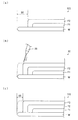
図9は、図3の塗布処理ユニット129への基板Wの搬入時における図7の搬送機構127のハンドH1の動作を説明するための図である。なお、図9では、搬送機構127および塗布処理ユニット129の構成の一部が上面図で示されている。また、搬送機構127のハンドH2の動作はハンドH1の動作と同様である。さらに、図6の搬送機構128,137,138のハンドH1,H2の動作は、搬送機構127のハンドH1,H2の動作と同様である。
(7)
図9(a)において、矢印で示されるように、ハンドH1により保持された基板Wが塗布処理ユニット129内に搬入される。ハンドH1とスピンチャック25との位置関係は予め設定されている。次に、図9(b)に示すように、塗布処理ユニット129に搬入される基板Wは、基板Wの中心W1がスピンチャック25の軸心P1と一致するようにスピンチャック25上に載置される。その後、図9(c)に示すように、ハンドH1が塗布処理ユニット129から搬出される。
In FIG. 9A, the substrate W held by the hand H1 is carried into the
塗布処理室22,24(図2)の塗布処理ユニット129においては、基板Wの表面上に反射防止液が塗布される。塗布処理室21,23(図2)の塗布処理ユニット129においては、基板W上に形成された反射防止膜上にレジスト液が塗布される。塗布処理室32,34(図2)の塗布処理ユニット129においては、基板W上に形成されたレジスト膜上にレジストカバー液が塗布される。
In the
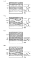
図10および図11は、基板Wの表面上への反射防止膜、レジスト膜およびレジストカバー膜の形成手順と各膜の除去範囲とを示す図である。 FIG. 10 and FIG. 11 are diagrams showing the formation procedure of the antireflection film, the resist film, and the resist cover film on the surface of the substrate W and the removal range of each film.
まず、塗布処理室21(または塗布処理室23)の塗布処理ユニット129において、基板Wが回転されつつ基板Wの表面上に反射防止液が塗布されるとともに、エッジリンスノズル30から基板Wの周縁部に向けてリンス液が吐出される。これにより、図10(a)に示すように、基板Wの周縁部に付着する反射防止液が溶解される。このようにして、基板Wの周縁部の環状領域における反射防止液が除去される。その後、熱処理部123により基板Wに所定の熱処理が行われることにより、図10(b)に示すように、周縁部を除く基板Wの表面上に反射防止膜F1が形成される。基板Wの外周部と反射防止膜F1の外周部との間の幅をエッジカット幅D1と呼ぶ。
First, in the
次に、塗布処理室22(または塗布処理室24)の塗布処理ユニット129において、基板Wが回転されつつ基板Wの表面上にレジスト液が塗布されるとともに、エッジリンスノズル30から基板Wの周縁部に向けてリンス液が吐出される。これにより、図10(c)に示すように、基板Wの周縁部に付着するレジスト液が溶解される。このようにして、基板Wの周縁部の環状領域におけるレジスト液が除去される。その後、熱処理部123により基板Wに所定の熱処理が行われることにより、図11(a)に示すように、周縁部を除く基板W上に反射防止膜F1上を覆うようにレジスト膜F2が形成される。基板Wの外周部とレジスト膜F2の外周部との間の幅をエッジカット幅D2と呼ぶ。
Next, in the
続いて、塗布処理室32(または塗布処理室34)の塗布処理ユニット129において、基板Wが回転されつつ基板Wの表面上にレジストカバー液が塗布されるとともに、エッジリンスノズル30から基板Wの周縁部に向けてリンス液が吐出される。これにより、図11(b)に示すように、基板Wの周縁部に付着するレジストカバー液が溶解される。このようにして、基板Wの周縁部の環状領域におけるレジストカバー液が除去される。その後、熱処理部133により基板Wに所定の熱処理が行われることにより、図11(c)に示すように、周縁部を除く基板W上にレジスト膜F2を覆うようにレジストカバー膜F3が形成される。基板Wの外周部とレジストカバー膜F3の外周部との間の幅をエッジカット幅D3と呼ぶ。
Subsequently, in the
図12は、反射防止膜F1、レジスト膜F2およびレジストカバー膜F3が形成された基板Wの平面図である。塗布処理ユニット129(図9)において、基板Wの中心W1がスピンチャック25(図9)の軸心P1と一致するようにスピンチャック25上に載置される。この状態で、エッジリンスノズル30から基板Wへ吐出されるリンス液の流量およびリンス液の吐出位置が適正である場合、図12(a)に示すように、基板Wの全周縁部上に渡ってエッジカット幅D1〜D3が均一な設定値となるように反射防止膜F1、レジスト膜F2およびレジストカバー膜F3が形成される。
FIG. 12 is a plan view of the substrate W on which the antireflection film F1, the resist film F2, and the resist cover film F3 are formed. In the coating processing unit 129 (FIG. 9), the substrate W is placed on the
一方、塗布処理ユニット129において、基板Wの中心W1がスピンチャック25の軸心P1に対して偏心するようにスピンチャック25上に載置された場合、図12(b)に示すように、エッジカット幅D1〜D3が不均一になるように基板W上に反射防止膜F1、レジスト膜F2およびレジストカバー膜F3が形成される。
On the other hand, when the
また、エッジリンスノズル30から基板Wへ吐出されるリンス液の流量が適正な値よりも小さい場合、リンス液が設定位置の内側までしみ込むため、図12(c)の点線で示すように、エッジカット幅D3が設定値よりも大きくなるようにレジストカバー膜F3が形成される。エッジリンスノズル30から基板Wへ吐出されるリンス液の流量が適正な値よりも大きい場合、リンス液の液幅が狭くなるため、図12(c)の一点鎖線で示すように、エッジカット幅D3が設定値よりも小さくなるようにレジストカバー膜F3が形成される。なお、図12(c)においては、反射防止膜F1、レジスト膜F2およびエッジカット幅D1,D2の図示は省略している。上記の場合、エッジカット幅D1,D2も設定値と異なる。
Further, when the flow rate of the rinsing liquid discharged from the
さらに、エッジリンスノズル30から基板Wへのリンス液の吐出位置が適正でない場合においても、エッジカット幅D1〜D3が設定値と異なるように反射防止膜F1,レジスト膜F2およびレジストカバー膜F3が形成される。
Further, even when the discharge position of the rinse liquid from the edge rinse
このように、基板Wのエッジカット幅D1〜D3を検出することにより、塗布処理ユニット129における基板Wの偏心量が許容上限値以下であるか否か、ならびにリンス液の流量および吐出位置が適正であるか否かを判定することができる。
Thus, by detecting the edge cut width D1~D3 the substrate W, whether the amount of eccentricity of the substrate W in the
(8)エッジ露光部の詳細
次に、エッジ露光部EEWの詳細について説明する。図13はエッジ露光部EEWの一側面を模式的に示す図であり、図14はエッジ露光部EEWの他の側面を模式的に示す図である。また、図15はエッジ露光部EEWの模式的平面図である。
(8) Details of Edge Exposure Unit Next, details of the edge exposure unit EEW will be described. FIG. 13 is a diagram schematically illustrating one side surface of the edge exposure unit EEW, and FIG. 14 is a diagram schematically illustrating another side surface of the edge exposure unit EEW. FIG. 15 is a schematic plan view of the edge exposure unit EEW.
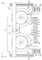
図13および図14に示すように、エッジ露光部EEWは、投光部510、投光部保持ユニット520、基板回転ユニット540および状態検出処理ユニット580を備える。また、状態検出処理ユニット580は、後述する図16の状態検出コントローラMCに接続される。
As shown in FIGS. 13 and 14, the edge exposure unit EEW includes a
投光部510は、光ファイバケーブル等からなるライトガイドを介して図示しない後述の露光用光源と接続されている。これにより、投光部510はライトガイドを介して露光用光源より送られる光を基板Wの周縁部に照射する。以下、基板W上のレジスト膜を露光するために投光部510により基板Wに照射される光を露光用光と呼ぶ。
The
投光部保持ユニット520は、X方向駆動モータ521、X方向ボールネジ522、投光部保持ガイド523、支柱524、Y方向駆動モータ531、支柱保持ガイド532およびY方向ボールネジ533を備える。
The light projecting
投光部保持ガイド523は、投光部510をX方向に移動可能に保持する。また、X方向ボールネジ522は、投光部510に設けられた図示しない連結部に螺合されている。
The light projecting
X方向ボールネジ522は、X方向に延びるように設けられており、X方向駆動モータ521の動作に伴って矢印R1の方向に回転する。X方向ボールネジ522が回転することにより、投光部510がX方向に移動する。
The X
X方向駆動モータ521および投光部保持ガイド523は、支柱524により所定の高さに支持されている。支柱524の下端部は支柱保持ガイド532により保持されている。支柱保持ガイド532は、支柱524をY方向に移動可能に保持する。また、Y方向ボールネジ533は、支柱524に設けられた図示しない連結部に螺合されている。
The
Y方向ボールネジ533は、Y方向に延びるように設けられており、Y方向駆動モータ531の動作に伴って矢印R3の方向に回転する。Y方向ボールネジ533が回転することにより、支柱524がY方向に移動する。
The Y
このように、投光部保持ユニット520の各部の動作により、投光部510がX方向およびY方向に移動する。
In this way, the
基板回転ユニット540は、基板回転モータ541、基板回転軸542およびスピンチャック543を備える。基板回転軸542は、基板回転モータ541から上方に突出する。スピンチャック543は、基板回転軸542の上端に接続されている。エッジ露光処理時には、スピンチャック543上に基板Wが載置される。スピンチャック543は、載置された基板Wを吸着保持する。
The
基板回転モータ541は、基板回転軸542を矢印R2の方向に回転させる。それにより、スピンチャック543が回転し、スピンチャック543により吸着保持された基板Wが回転する。
The
状態検出処理ユニット580は、照明部581、反射ミラー582およびCCD(電荷結合素子)ラインセンサ583を備える。
The state
図15に示すように、照明部581はY方向に沿うように基板Wの周縁部の上方に配置される。反射ミラー582は、照明部581と対向するように基板Wの上方に配置される。反射ミラー582の上方にCCDラインセンサ583が配置される。CCDラインセンサ583は、画素の配列方向がY方向に沿うように配置される。
As shown in FIG. 15, the
照明部581から基板Wの周縁部の状態を検出するための帯状の光(以下、照明光と呼ぶ。)が発生される。照明光は、基板Wの周縁部に照射される。照射された照明光は、基板W上で反射され、さらに反射ミラー582上で反射され、CCDラインセンサ583に投射される。CCDラインセンサ583の受光量分布は、基板Wの周縁部での反射光の明るさの分布に対応する。
Band-shaped light (hereinafter referred to as illumination light) for detecting the state of the peripheral edge of the substrate W is generated from the
ここで、基板Wの表面での反射光の明るさの分布は、基板Wの周縁部の状態によって異なる。具体的には、基板W上に反射防止膜F1、レジスト膜F2およびレジストカバー膜F3が形成されている場合、反射防止膜F1、レジスト膜F2およびレジストカバー膜F3の形成領域に応じて基板Wの表面での反射光の明るさの分布が異なる。 Here, the brightness distribution of the reflected light on the surface of the substrate W varies depending on the state of the peripheral edge of the substrate W. Specifically, when the antireflection film F1, the resist film F2, and the resist cover film F3 are formed on the substrate W, the substrate W is formed according to the formation region of the antireflection film F1, the resist film F2, and the resist cover film F3. The distribution of the brightness of the reflected light on the surface is different.
本実施の形態では、CCDラインセンサ583の受光量分布に基づいて、後述の基板の周縁部の状態検出処理が行われる。
In the present embodiment, a state detection process of the peripheral portion of the substrate, which will be described later, is performed based on the received light amount distribution of the
(9)基板処理システムの制御系の構成
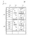
図16は、基板処理システム1000の制御系の構成を示すブロック図である。図16に示すように、ホストコンピュータ800は、メインコントローラ114に接続される。メインコントローラ114には、メインパネルPNおよび操作部90が接続される。また、メインコントローラ114には、ローカルコントローラLC1,LC2および状態検出コントローラMCが接続される。ユーザによる操作部90の操作情報がメインコントローラ114に与えられる。
(9) Configuration of Control System of Substrate Processing System FIG. 16 is a block diagram showing the configuration of the control system of the
ローカルコントローラLC1は、熱処理制御部C11、搬送制御部C12および塗布処理制御部C13を有する。熱処理制御部C11は、図4の熱処理部123における熱処理ユニットPHP、密着強化処理ユニットPAHPおよび冷却ユニットCPの温度を制御する。搬送制御部C12は、図6の搬送部122の搬送機構127,128の動作を制御する。
The local controller LC1 includes a heat treatment control unit C11, a transfer control unit C12, and a coating process control unit C13. The heat treatment control unit C11 controls the temperatures of the heat treatment unit PHP, the adhesion reinforcement processing unit PAHP, and the cooling unit CP in the
塗布処理制御部C13は、図2の塗布処理部121のノズル搬送機構29(図1)の動作、スピンチャック25の動作および各処理液ノズル28への処理液の供給を制御する。また、塗布処理制御部C13は、図3のリンス液供給系30bを制御することにより、エッジリンスノズル30へのリンス液の供給を制御するとともに、エッジリンスノズル30から基板Wへ吐出されるリンス液の流量を調整する。さらに、塗布処理制御部C13は、図3のエッジリンスノズル駆動部30aを制御することにより、エッジリンスノズル30の移動を制御するとともに、エッジリンスノズル30から基板Wへのリンス液の吐出位置を制御する。
The application processing control unit C13 controls the operation of the nozzle transport mechanism 29 (FIG. 1) of the
ローカルコントローラLC2は、熱処理制御部C21、搬送制御部C22、塗布現像処理制御部C23およびエッジ露光制御部C24を有する。熱処理制御部C21は、図4の熱処理部133における熱処理ユニットPHPおよび冷却ユニットCPの温度を制御する。搬送制御部C22は、図6の搬送部132の搬送機構137,138の動作を制御する。
The local controller LC2 includes a heat treatment control unit C21, a conveyance control unit C22, a coating and developing process control unit C23, and an edge exposure control unit C24. The heat treatment control unit C21 controls the temperatures of the heat treatment unit PHP and the cooling unit CP in the
塗布現像処理制御部C23は、図2の塗布現像処理部131のノズル搬送機構29(図1)の動作、移動機構39の動作、スピンチャック25,35の動作、各処理液ノズル28への処理液の供給および各スリットノズル38への現像液の供給を制御する。
The coating / developing process control unit C23 operates the nozzle transport mechanism 29 (FIG. 1) of the coating / developing
また、塗布現像処理制御部C23は、図3のリンス液供給系30bを制御することにより、エッジリンスノズル30へのリンス液の供給を制御するとともに、エッジリンスノズル30から基板Wへ吐出されるリンス液の流量を調整する。さらに、塗布現像処理制御部C23は、図3のエッジリンスノズル駆動部30aを制御することにより、エッジリンスノズル30の移動を制御するとともに、エッジリンスノズル30から基板Wへのリンス液の吐出位置を制御する。
Further, the coating and developing treatment control unit C23 controls the rinsing
エッジ露光制御部C24は、X方向駆動モータ521(図13)の動作、Y方向駆動モータ531(図13)の動作、基板回転モータ541の動作(図13)および露光用光源(図示せず)の動作を制御する。 The edge exposure controller C24 operates the X-direction drive motor 521 (FIG. 13), the Y-direction drive motor 531 (FIG. 13), the substrate rotation motor 541 (FIG. 13), and an exposure light source (not shown). To control the operation.
状態検出コントローラMCは、照明制御部C31およびCCDラインセンサ制御部C32を有する。照明制御部C31は、図13の照明部581の動作を制御する。CCDラインセンサ制御部C32は、図13のCCDラインセンサ583の動作を制御する。
The state detection controller MC includes an illumination control unit C31 and a CCD line sensor control unit C32. The illumination control unit C31 controls the operation of the
(10)基板の周縁部の状態検出処理
基板Wの周縁部の状態検出処理について説明する。状態検出処理では、CCDラインセンサ583の受光量分布が状態検出コントローラMCを介してメインコントローラ114に与えられる。CCDラインセンサ583の受光量分布に基づいて、基板Wの周縁部の状態(エッジカット幅D1〜D3)の検査が行われる。
(10) State detection process of peripheral edge of substrate The state detection process of the peripheral edge of the substrate W will be described. In the state detection process, the received light amount distribution of the
上記のように、CCDラインセンサ583の受光量分布は、基板Wの周縁部での反射光の明るさの分布に対応する。基板Wが1回転することにより、基板Wの周縁部の全体に照明光が照射される。基板Wが1回転する期間に、CCDラインセンサ583の受光量分布が連続的にメインコントローラ114に与えられる。メインコントローラ114は、CCDラインセンサ583の受光量分布に基づいて、基板Wの周縁部の全体での反射光の明るさの分布を示す周縁部画像データを作成する。
As described above, the received light amount distribution of the
図17は、周縁部画像データの作成方法について説明するための図である。図17(a),(b),(c)には、基板W上における照明光の照射状態が順に示され、図17(d),(e),(f)には、図17(a),(b),(c)の状態で作成される周縁部画像データがそれぞれ示される。なお、図17(a)〜(c)において、照明光が照射された基板W上の領域にハッチングが付される。また、図17(d)〜(f)においては、理解を容易にするために、周縁部画像データがその周縁部画像データに基づいて表示される画像の形態で表示される。 FIG. 17 is a diagram for explaining a method of creating peripheral edge image data. FIGS. 17A, 17B, and 17C sequentially show the illumination light irradiation states on the substrate W. FIGS. 17D, 17E, and 17F show FIGS. ), (B), and (c) are respectively shown peripheral edge image data created. In FIGS. 17A to 17C, the region on the substrate W irradiated with the illumination light is hatched. In FIGS. 17D to 17F, the peripheral edge image data is displayed in the form of an image displayed based on the peripheral edge image data for easy understanding.
図17(a)〜(c)に示すように、基板W上の周縁部に継続的に照明光が照射されつつ基板Wが回転する。それにより、基板Wの周方向に連続的に照明光が照射される。基板Wが1回転すると、基板Wの周縁部の全体に照明光が照射される。 As shown in FIGS. 17A to 17C, the substrate W rotates while the illumination light is continuously applied to the peripheral portion on the substrate W. Thereby, illumination light is continuously irradiated in the circumferential direction of the substrate W. When the substrate W rotates once, the illumination light is irradiated to the entire periphery of the substrate W.
基板Wが1回転する期間に連続的に得られるCCDラインセンサ583の受光量分布に基づいて、図17(d)〜(f)に示すように、矩形の周縁部画像データd1が作成される。
As shown in FIGS. 17D to 17F, rectangular peripheral edge image data d1 is created based on the received light amount distribution of the
周縁部画像データd1の縦方向の位置は、CCDラインセンサ583の各画素の位置(基板Wの半径方向の位置)に対応し、周縁部画像データd1の横方向の位置は、基板Wの回転角度に対応する。 The vertical position of the peripheral image data d1 corresponds to the position of each pixel of the CCD line sensor 583 (the radial position of the substrate W), and the horizontal position of the peripheral image data d1 is the rotation of the substrate W. Corresponds to the angle.
この場合、周縁部画像データd1の縦方向の変化は、基板Wの周縁部の領域T1での基板Wの半径方向における反射光の明るさの分布を表わす。また、周縁部画像データd1の横方向の変化は、基板Wの周方向における基板Wの周縁部の領域T1での反射光の明るさの分布を表わす。また、周縁部画像データd1における基板Wの外周部EDGの位置からの距離に基づいて、エッジカット幅D1〜D3を算出することができる。 In this case, the change in the vertical direction of the peripheral edge image data d1 represents the distribution of the brightness of the reflected light in the radial direction of the substrate W in the peripheral region T1 of the substrate W. The change in the lateral direction of the peripheral edge image data d1 represents the distribution of the brightness of the reflected light in the region T1 of the peripheral edge of the substrate W in the circumferential direction of the substrate W. Further, the edge cut widths D1 to D3 can be calculated based on the distance from the position of the outer peripheral portion EDG of the substrate W in the peripheral portion image data d1.
基板Wが1回転した時点で、基板Wの周縁部全体での反射光の明るさの分布が1つの矩形の周縁部画像データd1として得られる。周縁部画像データd1に基づいて基板Wの周縁部の画像(以下、周縁部画像と呼ぶ。)が表示される。 When the substrate W rotates once, the brightness distribution of the reflected light over the entire periphery of the substrate W is obtained as one rectangular periphery image data d1. Based on the peripheral edge image data d1, an image of the peripheral edge of the substrate W (hereinafter referred to as a peripheral edge image) is displayed.
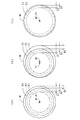
図18は、周縁部画像データd1に基づいて表示される周縁部画像の明るさの分布を示す図である。図18(a)の例では、基板Wの全周縁部上に渡ってエッジカット幅D1〜D3がほぼ一定で許容範囲内にある。この場合、スピンチャック25上の基板Wの偏心量が許容上限値以下であり、かつエッジリンスノズル30から基板Wへ吐出されるリンス液の流量およびリンス液の吐出位置が適正であったと判定される。
FIG. 18 is a diagram illustrating the brightness distribution of the peripheral edge image displayed based on the peripheral edge image data d1. In the example of FIG. 18A, the edge cut widths D1 to D3 are substantially constant and within the allowable range over the entire peripheral edge of the substrate W. In this case, it is determined that the eccentric amount of the substrate W on the
図18(b)の例では、基板Wの全周縁部上に渡ってエッジカット幅D1〜D3の平均値は許容範囲内にあるが、エッジカット幅D1〜D3が大きく変化している。この場合、エッジリンスノズル30から基板Wへ吐出されるリンス液の流量およびリンス液の吐出位置は適正であったが、スピンチャック25上の基板Wの偏心量が許容上限値を超えていたと判定される。
In the example of FIG. 18B, the average values of the edge cut widths D1 to D3 are within the allowable range over the entire peripheral edge of the substrate W, but the edge cut widths D1 to D3 are greatly changed. In this case, the flow rate of the rinse liquid discharged from the edge rinse
図18(c)の例では、基板Wの全周縁部上に渡ってエッジカット幅D1〜D3がほぼ一定であるが、許容範囲の下限値よりも小さい。この場合、スピンチャック25上の基板Wの偏心量は許容上限値以下であるが、エッジリンスノズル30から基板Wへ吐出されるリンス液の流量またはリンス液の吐出位置が適正でなかったと判定される。
In the example of FIG. 18C, the edge cut widths D1 to D3 are substantially constant over the entire peripheral edge of the substrate W, but are smaller than the lower limit value of the allowable range. In this case, the eccentric amount of the substrate W on the
図18(d)の例では、基板Wの全周縁部上に渡ってエッジカット幅D1〜D3が大きく変化し、かつエッジカット幅D1〜D3の平均値は許容範囲の下限値よりも小さい。この場合、スピンチャック25上の基板Wの偏心量が許容上限値を超え、かつエッジリンスノズル30から基板Wへ吐出されるリンス液の流量またはリンス液の吐出位置が適正でなかったと判定される。
In the example of FIG. 18D, the edge cut widths D1 to D3 vary greatly over the entire peripheral edge of the substrate W, and the average value of the edge cut widths D1 to D3 is smaller than the lower limit value of the allowable range. In this case, it is determined that the eccentric amount of the substrate W on the
図19および図20は、図16のメインコントローラ114の動作を示すフローチャートである。以下の説明では、エッジカット幅D1についての基板の周縁部の状態検出処理を説明するが、エッジカット幅D2,D3についての基板の周縁部の状態検出処理もエッジカット幅D1についての基板の周縁部の状態検出処理と同様である。
19 and 20 are flowcharts showing the operation of the
まず、メインコントローラ114は、ローカルコントローラLC2および搬送制御部C22を通して図6の搬送機構137を制御することにより、図13のエッジ露光部EEWのスピンチャック543上に基板Wを載置させる。また、メインコントローラ114は、ローカルコントローラLC2およびエッジ露光制御部C24を通して図13のスピンチャック543を制御することにより、スピンチャック543上に基板Wを吸着保持させる(ステップS1)。
First, the
次に、メインコントローラ114は、ローカルコントローラLC2およびエッジ露光制御部C24を通してスピンチャック543を制御することにより、スピンチャック543に保持された基板Wを1回転させる(ステップS2)。基板Wが1回転する期間に、メインコントローラ114は、図13のCCDラインセンサ583の受光量分布に基づいて、周縁部画像データd1を作成する(ステップS3)。
Next, the
次に、メインコントローラ114は、作成した周縁部画像データd1を図16のホストコンピュータ800に送信する(ステップS4)。ホストコンピュータ800は、メインコントローラ114からの周縁部画像データd1を記憶する。ユーザは、ホストコンピュータ800またはそのホストコンピュータ800に接続された端末装置により、必要に応じて周縁部画像データd1を確認することができる。
Next, the
なお、メインコントローラ114が周縁部画像データd1を記憶してもよい。その場合、ユーザが必要に応じて図1のメインパネルPNにより周縁部画像データd1を確認することができる。また、任意のタイミングでメインコントローラ114からホストコンピュータ800に周縁部画像データd1を送信することができる。
The
続いて、メインコントローラ114は、作成した周縁部画像データd1に基づいて、エッジカット幅D1の平均値を算出する(ステップS5)。また、メインコントローラ114は、作成した周縁部画像データd1に基づいて、エッジカット幅D1の最大値と最小値との差を算出する(ステップS6)。エッジカット幅D1の最大値と最小値との差は、エッジカット幅D1のばらつき(変化量)に相当する。
Subsequently, the
次に、メインコントローラ114は、基板WのステップS5で算出されたエッジカット幅D1の平均値が予め設定された許容範囲内であるか否かを判定する(ステップS7)。エッジカット幅D1の平均値が許容範囲内である場合、メインコントローラ114は、図2の塗布処理室21(または塗布処理室23)のエッジリンスノズル30から基板Wへ吐出されたリンス液の流量およびリンス液の吐出位置が適正であったと判定する。
Next, the
さらに、メインコントローラ114は、ステップS6で算出されたエッジカット幅D1の差が予め設定されたしきい値以下であるか否かを判定する(ステップS8)。エッジカット幅D1の差がしきい以下である場合、メインコントローラ114は、図2の塗布処理室21(または塗布処理室23)において、スピンチャック25上の基板Wの偏心量が許容上限値以下であったと判定する。このときの基板Wの周縁部画像データd1に基づく周縁部画像は、図18(a)のようになる。その後、メインコントローラ114は、基板Wの周縁部の状態検出処理を終了する。
Further, the
ステップS8において、エッジカット幅D1の差がしきい値を超える場合、メインコントローラ114は、塗布処理室21(または塗布処理室23)において、スピンチャック25上の基板Wの偏心量が許容上限値を超えていたと判定する。このときの基板Wの周縁部画像データd1に基づく周縁部画像は、図18(b)のようになる。
If the difference in the edge cut width D1 exceeds the threshold value in step S8, the
この場合、メインコントローラ114は、塗布処理室21(または塗布処理室23)のスピンチャック25上の基板Wの偏心量が小さくなるように、ローカルコントローラLC1および搬送制御部C12を通して搬送機構127(または搬送機構128)の動作を補正する(ステップS9)。その後、メインコントローラ114は、基板Wの周縁部の状態検出処理を終了する。
In this case, the
ステップS7において、エッジカット幅D1の平均値が許容範囲外である場合、メインコントローラ114は、図2の塗布処理室21(または塗布処理室23)のエッジリンスノズル30から基板Wへのリンス液の流量またはリンス液の吐出位置が適正でなかったと判定する。
In step S7, when the average value of the edge cut width D1 is outside the allowable range, the
この場合、メインコントローラ114は、ステップS6で算出されたエッジカット幅D1の差がしきい値以下であるか否かを判定する(ステップS10)。エッジカット幅D1の差がしきい以下である場合、メインコントローラ114は、図2の塗布処理室21(または塗布処理室23)において、スピンチャック25上の基板Wの偏心量が許容上限値以下であったと判定する。このときの基板Wの周縁部画像データd1に基づく周縁部画像は、図18(c)のようになる。
In this case, the
その後、メインコントローラ114は、図3のリンス液供給系30bにおける流量センサにより測定されるリンス液の流量が設定値に等しいか否かを判定する(ステップS11)。リンス液の流量が設定値とは異なる場合、メインコントローラ114は、警報を出力する(ステップS12)。警報の出力としては、例えばブザー等による警報音の発生、またはランプ等による警報表示が行われる。その後、メインコントローラ114は、基板Wの周縁部の状態検出処理を終了する。
Thereafter, the
ステップS11において、リンス液の流量が設定値に等しい場合、メインコントローラ114は、エッジリンスノズル30からのリンス液の吐出位置が適正でなかったと判定する。この場合、メインコントローラ114は、ローカルコントローラLC1および塗布処理制御部C13を通して図3のエッジリンスノズル駆動部30aを制御することにより、エッジリンスノズル30からのリンス液の吐出位置を調整する(ステップS13)。例えば、ステップS5において算出されたエッジカット幅D1の平均値が許容範囲の下限値よりも小さい場合には、メインコントローラ114は、エッジリンスノズル30を基板Wの中心に近づく方向に一定量移動させる。逆に、ステップS5において算出されたエッジカット幅D1の平均値が許容範囲の上限値よりも大きい場合には、メインコントローラ114は、エッジリンスノズル30を基板Wの中心から遠ざかる方向に一定量移動させる。その後、メインコントローラ114は、基板Wの周縁部の状態検出処理を終了する。
In step S11, when the flow rate of the rinse liquid is equal to the set value, the
ステップS10において、エッジカット幅D1の差がしきい値を超える場合、メインコントローラ114は、塗布処理室21(または塗布処理室23)において、スピンチャック25上の基板Wの偏心量が許容上限値を超えていたと判定する。このときの基板Wの周縁部画像データd1に基づく周縁部画像は、図18(d)のようになる。この場合、メインコントローラ114は、塗布処理室21(または塗布処理室23)のスピンチャック25上の基板Wの偏心量が小さくなるように、ローカルコントローラLC1および搬送制御部C12を通して搬送機構127(または搬送機構128)の動作を補正する(ステップS14)。
If the difference in the edge cut width D1 exceeds the threshold value in step S10, the
その後、メインコントローラ114は、図3のリンス液供給系30bにおける流量センサにより測定されるリンス液の流量が設定値に等しいか否かを判定する(ステップS15)。リンス液の流量が設定値とは異なる場合、メインコントローラ114は、警報を出力する(ステップS16)。その後、メインコントローラ114は、基板Wの周縁部の状態検出処理を終了する。
Thereafter, the
ステップS15において、リンス液の流量が設定値に等しい場合、メインコントローラ114は、ローカルコントローラLC1および塗布処理制御部C13を通して図3のエッジリンスノズル駆動部30aを制御することにより、エッジリンスノズル30からのリンス液の吐出位置を調整する(ステップS17)。その後、メインコントローラ114は、基板Wの周縁部の状態検出処理を終了する。
In step S15, when the flow rate of the rinsing liquid is equal to the set value, the
なお、図18の例では、周縁部画像データd1における基板Wの外周部EDGが直線となっているが、エッジ露光部EEWにおいてスピンチャック543の軸心に対して基板Wの中心が偏心している場合には、周縁部画像データd1における基板Wの外周部EDGは直線とはならない。この場合においても、エッジカット幅D1〜D3に基づいてスピンチャック25上の基板Wの偏心量ならびにエッジリンスノズル30から基板Wへ吐出されるリンス液の流量および吐出位置を判定することができる。
In the example of FIG. 18, the outer peripheral portion EDG of the substrate W in the peripheral edge image data d1 is a straight line, but the center of the substrate W is decentered with respect to the axis of the
(11)効果
本実施の形態に係る基板処理装置100においては、状態検出処理ユニット580の画像処理により基板Wのエッジカット幅D1〜D3が容易に検出される。メインコントローラ114は、検出された各エッジカット幅D1〜D3の最大値と最小値との差がしきい値以下か否かを判定することにより、基板Wの中心W1がスピンチャック25の軸心P1に対して偏心するようにスピンチャック25上に載置されたことを確実に検出することができる。
(11) Effects In the
基板Wの中心W1がスピンチャック25の軸心P1に対して偏心するようにスピンチャック25上に載置されたことを検出した場合、メインコントローラ114は、スピンチャック25上の基板Wの偏心量が小さくなるように、ローカルコントローラLC1,LC2および搬送制御部C12,C22を通して搬送機構127,128,137,138の動作を補正する。これにより、基板処理の精度を向上させることができる。
When it is detected that the center W1 of the substrate W is placed on the
また、メインコントローラ114は、各エッジカット幅D1〜D3の平均値が許容範囲内か否かを判定することにより、塗布処理ユニット129におけるエッジリンスノズル30から基板Wへ吐出されるリンス液の流量またはリンス液の吐出位置が適正でないことを確実に検出することができる。
Further, the
エッジリンスノズル30から基板Wへ吐出されるリンス液の流量が適正でないことを検出した場合、メインコントローラ114は警報を出力することにより、作業者にリンス液の流量が適正でないことを知らせることができる。それにより、作業者は、各エッジカット幅D1〜D3の平均値が許容範囲内になるようにリンス液の流量の設定値を調整するか、またはリンス液供給系30bのメンテナンスを行うことによりリンス液の流量を適正にすることができる。これにより、基板処理の精度を向上させることができる。
When the
リンス液の吐出位置が適正でないことを検出した場合、メインコントローラ114は、ローカルコントローラLC1,LC2、塗布処理制御部C13および塗布現像処理制御部C23を通して図3のエッジリンスノズル駆動部30aを制御することにより、エッジリンスノズル30からのリンス液の吐出位置を調整する。これにより、基板処理の精度を向上させることができる。
When it is detected that the discharge position of the rinse liquid is not appropriate, the
上記の基板Wの周縁部の状態検出処理は、基板処理装置100の稼働時間外の基板処理装置100のティーチング時またはメンテナンス時に行われてもよく、あるいは基板処理装置100の稼動時間内に行われてもよい。
The state detection processing of the peripheral portion of the substrate W may be performed during teaching or maintenance of the
(12)他の実施の形態
(12−1)上記実施の形態において、メインコントローラ114は、基板Wの周縁部の状態検出処理におけるステップS9またはステップS14の処理で、エッジカット幅D1の最大値と最小値との差が予め設定されたしきい値を超えた場合、搬送機構127の動作を補正するが、これに限定されない。エッジカット幅D1の最大値と最小値との差が予め設定されたしきい値を超えた場合、メインコントローラ114は、ステップS9またはステップS14の処理の代わりに警報を出力してもよい。それにより、作業者は、基板Wの中心W1がスピンチャック25の軸心P1に対して偏心するようにスピンチャック25上に載置されたことを認識することができる。この場合、作業者は、基板Wの中心W1がスピンチャック25の軸心P1に一致するように搬送機構127を調整することができる。
(12) Other Embodiments (12-1) In the above embodiment, the
(12−2)上記実施の形態において、メインコントローラ114は、基板Wの周縁部の状態検出処理におけるステップS12またはステップS16の処理で、リンス液の流量が設定値とは異なる場合、警報を出力するが、これに限定されない。リンス液の流量が設定値とは異なる場合、メインコントローラ114は、ステップS12またはステップS16の処理の代わりにエッジカット幅D1の平均値が許容範囲内になるようにリンス液供給系30bにおけるリンス液の流量を調整してもよい。
(12-2) In the above embodiment, the
(12−3)上記実施の形態において、メインコントローラ114は、基板Wの周縁部の状態検出処理のステップS13またはステップS17の処理で、リンス液の流量が設定値に等しい場合、リンス液の吐出位置を調整するが、これに限定されない。リンス液の流量が設定値とは異なる場合、メインコントローラ114は、ステップS13またはステップS17の処理の代わりに警報を出力してもよい。それにより、作業者は、リンス液の吐出位置が適正でないことを認識することができる。この場合、作業者は、エッジリンスノズル駆動部30aのメンテナンスを行うことによりリンス液の吐出位置を適正にすることができる。
(12-3) In the above embodiment, the
(12−4)上記実施の形態において、状態検出処理ユニット580はエッジ露光部EEWに設けられるが、これに限定されない。状態検出処理ユニット580は、例えば塗布処理ユニット129または現像処理ユニット139等の他のユニットに設けられてもよい。
(12-4) In the above embodiment, the state
また、状態検出処理ユニット580として基板の表面状態を検査するマクロ検査装置が設けられてもよい。この場合、マクロ検査装置のCCDカメラにより基板Wの表面が撮像される。撮像された基板Wの表面の画像に基づいて、エッジカット幅D1〜D3が算出される。
Further, a macro inspection apparatus that inspects the surface state of the substrate may be provided as the state
(13)請求項の各構成要素と実施の形態の各要素との対応
以下、請求項の各構成要素と実施の形態の各要素との対応の例について説明するが、本発明は下記の例に限定されない。
(13) Correspondence between each constituent element of claim and each element of the embodiment Hereinafter, an example of correspondence between each constituent element of the claim and each element of the embodiment will be described. It is not limited to.
上記の実施の形態では、基板Wが基板の例であり、基板処理装置100が基板処理装置の例であり、塗布処理ユニット129が膜形成ユニットの例であり、エッジ露光部EEWが検出ユニットおよびエッジ露光部の例であり、メインコントローラ114が制御部の例である。スピンチャック25が第1の回転保持装置の例であり、処理液ノズル28が処理液供給部の例であり、エッジリンスノズル30が除去液供給部の例である。
In the above embodiment, the substrate W is an example of a substrate, the
スピンチャック543が第2の回転保持装置の例であり、状態検出処理ユニット580が位置検出部の例であり、周縁部画像データd1が画像データの例であり、CCDラインセンサ583が画像データ検出部の例であり、エッジカット幅D1〜D3が幅の例である。ハンドH1,H2が保持部の例であり、搬送機構127,128,137,138が基板搬送装置の例である。
The
請求項の各構成要素として、請求項に記載されている構成または機能を有する他の種々の要素を用いることもできる。 As each constituent element in the claims, various other elements having configurations or functions described in the claims can be used.
本発明は、種々の基板の処理に有効に利用することができる。 The present invention can be effectively used for processing various substrates.
11 インデクサブロック
12 第1の処理ブロック
13 第2の処理ブロック
14A 洗浄乾燥処理ブロック
14B 搬入搬出ブロック
14 インターフェイスブロック
15 露光装置
15a 基板搬入部
15b 基板搬出部
21〜24,32,34 塗布処理室
25,35,543 スピンチャック
27,37 カップ
28 処理液ノズル
28a 把持部
29 ノズル搬送機構
30 エッジリンスノズル
30a エッジリンスノズル駆動部
30b リンス液供給系
31,33 現像処理室
38 スリットノズル
39 移動機構
41,43,45〜47 給気ユニット
42,44,48 排気ユニット
50,60 流体ボックス部
100 基板処理装置
111 キャリア載置部
112,122,132,163 搬送部
113 キャリア
114 メインコントローラ
115,127,128,137,138,141,142,146 搬送機構
116,H1〜H6 ハンド
121 塗布処理部
123,133 熱処理部
125,135 上段搬送室
126,136 下段搬送室
129 塗布処理ユニット
131 塗布現像処理部
139 現像処理ユニット
145 パッキン
161,162 洗浄乾燥処理部
280 待機部
291〜293 把持部移動機構
291a ノズル把持部
291b 挟持アーム
292a,293a ボールねじ
292b,293b ガイド
301,303 上段熱処理部
302,304 下段熱処理部
311〜313 ガイドレール
314 移動部材
315 回転部材
510 投光部
520 投光部保持ユニット
521 X方向駆動モータ
522 X方向ボールネジ
523 投光部保持ガイド
524 支柱
531 Y方向駆動モータ
532 支柱保持ガイド
533 Y方向ボールネジ
540 基板回転ユニット
541 基板回転モータ
542 基板回転軸
580 状態検出処理ユニット
581 照明部
582 反射ミラー
583 CCDラインセンサ
800 ホストコンピュータ
1000 基板処理システム
CP 冷却ユニット
D1〜D3 エッジカット幅
d1 周縁部画像データ
EDG 外周部
EEW エッジ露光部
F1 反射防止膜
F2 レジスト膜
F3 レジストカバー膜
H1〜H6 ハンド
MC 状態検出コントローラ
P1 軸心
P−BF1,P−BF2 載置兼バッファ部
P−CP 載置兼冷却部
PAHP 密着強化処理ユニット
PASS1〜PASS9 基板載置部
PHP 熱処理ユニット
PN メインパネル
R1〜R3 矢印
SD1,SD2 洗浄乾燥処理ユニット
T1 領域
W 基板
W1 中心
DESCRIPTION OF SYMBOLS 11 Indexer block 12 1st process block 13 2nd process block 14A Washing drying process block 14B Loading / unloading block 14 Interface block 15 Exposure apparatus 15a Substrate carrying-in part 15b Substrate carrying-out part 21-24, 32, 34 Coating process chamber 25, 35, 543 Spin chuck 27, 37 Cup 28 Processing liquid nozzle 28a Grasping part 29 Nozzle transport mechanism 30 Edge rinse nozzle 30a Edge rinse nozzle drive part 30b Rinse liquid supply system 31, 33 Development processing chamber 38 Slit nozzle 39 Moving mechanism 41, 43 , 45 to 47 Air supply unit 42, 44, 48 Exhaust unit 50, 60 Fluid box unit 100 Substrate processing device 111 Carrier placement unit 112, 122, 132, 163 Transport unit 113 Carrier 114 Main controller La 115, 127, 128, 137, 138, 141, 142, 146 Conveying mechanism 116, H1 to H6 Hand 121 Coating processing section 123, 133 Heat treatment section 125, 135 Upper transport chamber 126, 136 Lower transport chamber 129 Coating processing unit 131 Coating development processing unit 139 Development processing unit 145 Packing 161, 162 Cleaning / drying processing unit 280 Standby unit 291-293 Holding unit moving mechanism 291a Nozzle holding unit 291b Nipping arm 292a, 293a Ball screw 292b, 293b Guide 301, 303 Upper heat processing unit 302 , 304 Lower heat treatment part 311 to 313 Guide rail 314 Moving member 315 Rotating member 510 Light projecting part 520 Light projecting part holding unit 521 X direction drive motor 522 X direction ball screw 523 Light projecting part holding guide 5 4 support 531 Y-direction drive motor 532 support support guide 533 Y-direction ball screw 540 substrate rotation unit 541 substrate rotation motor 542 substrate rotation axis 580 state detection processing unit 581 illumination unit 582 reflection mirror 583 CCD line sensor 800 host computer 1000 substrate processing system CP Cooling unit
D1 to D3 Edge cut width d1 Peripheral part image data EDG Peripheral part EEW Edge exposure part F1 Antireflection film F2 Resist film F3 Resist cover film H1 to H6 Hand MC State detection controller P1 Axis center P-BF1, P-BF2 Buffer part P-CP Placement / cooling part PAHP Adhesion strengthening processing unit PASS1 to PASS9 Substrate placement part PHP Heat treatment unit PN Main panel R1 to R3 Arrow SD1, SD2 Cleaning / drying processing unit T1 region W substrate W1 center
Claims (8)
基板上に処理液の膜を形成する膜形成ユニットと、
前記膜形成ユニットによる膜形成後の基板の状態を検出する検出ユニットと、
前記検出ユニットの検出結果に基づく判定を行う制御部とを備え、
前記膜形成ユニットは、
基板を保持して回転させる第1の回転保持装置と、
前記第1の回転保持装置により回転される基板上に処理液を供給することにより処理液の膜を形成する処理液供給部と、
前記第1の回転保持装置により回転される基板の周縁部に除去液を供給することにより基板の周縁部上の処理液を除去する除去液供給部とを含み、
前記検出ユニットは、
基板を保持して回転させる第2の回転保持装置と、
前記第2の回転保持装置により回転される基板の外周部の位置および基板上の膜の外周部の位置を検出する位置検出部とを備え、
前記制御部は、前記位置検出部により検出された基板の外周部の位置および基板上の膜の外周部の位置に基づいて前記第1の回転保持装置の回転中心に対する前記第1の回転保持装置に保持された基板の中心の位置ずれを判定するとともに、前記膜形成ユニットにおける前記除去液供給部による除去液の供給状態を判定し、
前記除去液の供給状態は、前記除去液供給部により基板の外周部に供給される除去液の流量および前記除去液供給部による基板の外周部への除去液の供給位置の少なくとも一方を含むことを特徴とする基板処理装置。 A substrate processing apparatus for processing a substrate having at least a part of a circular outer periphery,
A film forming unit for forming a film of a processing solution on a substrate;
A detection unit for detecting a state of the substrate after film formation by the film formation unit;
A control unit that performs a determination based on the detection result of the detection unit,
The film forming unit includes:
A first rotation holding device for holding and rotating the substrate;
A processing liquid supply unit that forms a film of the processing liquid by supplying the processing liquid onto the substrate rotated by the first rotation holding device;
A removal liquid supply unit that removes the processing liquid on the periphery of the substrate by supplying the removal liquid to the periphery of the substrate rotated by the first rotation holding device;
The detection unit is
A second rotation holding device for holding and rotating the substrate;
A position detection unit that detects the position of the outer periphery of the substrate rotated by the second rotation holding device and the position of the outer periphery of the film on the substrate;
The first rotation holding device with respect to the rotation center of the first rotation holding device based on the position of the outer peripheral portion of the substrate and the position of the outer peripheral portion of the film on the substrate detected by the position detection portion. Determining the position shift of the center of the substrate held in the film, and determining the supply state of the removal liquid by the removal liquid supply unit in the film forming unit ,
The supply state of the removal liquid includes at least one of a flow rate of the removal liquid supplied to the outer peripheral part of the substrate by the removal liquid supply part and a supply position of the removal liquid to the outer peripheral part of the substrate by the removal liquid supply part. A substrate processing apparatus.
前記第2の回転保持装置により回転される基板の外周部の位置および基板上の膜の外周部の位置を示す画像データを検出する画像データ検出部を含み、
前記制御部は、前記画像検出部により検出された画像データに基づいて基板の半径方向における基板の外周部の位置の変化および基板上の膜の外周部の位置の変化を検出し、検出された基板の外周部の位置の変化および基板上の膜の外周部の位置の変化に基づいて前記基板の中心の位置ずれを判定するとともに、前記除去液の供給状態を判定することを特徴とする請求項1記載の基板処理装置。 The position detector is
An image data detection unit that detects image data indicating a position of an outer peripheral portion of the substrate rotated by the second rotation holding device and a position of the outer peripheral portion of the film on the substrate;
The control unit detects and detects a change in the position of the outer peripheral portion of the substrate in the radial direction of the substrate and a change in the position of the outer peripheral portion of the film on the substrate based on the image data detected by the image detection unit. The position of the center of the substrate is determined based on a change in the position of the outer peripheral portion of the substrate and a change in the position of the outer peripheral portion of the film on the substrate, and the supply state of the removal liquid is determined. Item 2. The substrate processing apparatus according to Item 1.
前記制御部は、前記基板の中心の位置ずれの判定結果に基づいて前記搬送装置の前記保持部による前記第1の回転保持装置への基板の載置動作を調整することを特徴とする請求項1〜4のいずれかに記載の基板処理装置。 A substrate transport apparatus including a holding unit that holds and transports the substrate and places the held substrate on the first rotation holding device of the film forming unit;
The said control part adjusts the mounting operation | movement of the board | substrate to the said 1st rotation holding apparatus by the said holding part of the said conveying apparatus based on the determination result of the position shift of the center of the said board | substrate. The substrate processing apparatus in any one of 1-4 .
前記検出ユニットは、基板上の膜の周縁部の露光処理を行う機能をさらに有するエッジ露光部であることを特徴とする請求項1〜6のいずれかに記載の基板処理装置。 The film forming unit forms a photosensitive film as a film of the treatment liquid,
Said detection unit, a substrate processing apparatus according to any one of claims 1 to 6, characterized in that an edge exposure unit further has a function of performing exposure processing of the peripheral edge of the film on the substrate.
膜形成ユニットにおける第1の回転保持装置により基板を保持して回転させるステップと、
前記第1の回転保持装置により回転される基板上に前記膜形成ユニットにおける処理液供給部により処理液を供給することにより処理液の膜を形成するステップと、
前記第1の回転保持装置により回転される基板の周縁部に前記膜形成ユニットにおける除去液供給部により除去液を供給することにより基板の周縁部上の処理液を除去するステップと、
検出ユニットにおける第2の回転保持装置により基板を保持して回転させるステップと、
前記第2の回転保持装置により回転される基板の外周部の位置および基板上の膜の外周部の位置を検出するステップと、
前記検出された基板の外周部の位置および基板上の膜の外周部の位置に基づいて前記第1の回転保持装置の回転中心に対する前記第1の回転保持装置に保持された基板の中心の位置ずれを判定するとともに、前記膜形成ユニットにおける前記除去液供給部による除去液の供給状態を判定するステップとを含み、
前記除去液の供給状態は、前記除去液供給部により基板の外周部に供給される除去液の流量および前記除去液供給部による基板の外周部への除去液の供給位置の少なくとも一方を含むことを特徴とする基板処理方法。 A substrate processing method for processing a substrate having at least a part of a circular outer periphery,
Holding and rotating the substrate by the first rotation holding device in the film forming unit;
Forming a film of the processing liquid on the substrate rotated by the first rotation holding device by supplying the processing liquid by the processing liquid supply unit in the film forming unit;
Removing the treatment liquid on the peripheral edge of the substrate by supplying the removal liquid to the peripheral edge of the substrate rotated by the first rotation holding device by the removal liquid supply section in the film forming unit;
Holding and rotating the substrate by the second rotation holding device in the detection unit;
Detecting the position of the outer peripheral portion of the substrate rotated by the second rotary holding device and the position of the outer peripheral portion of the film on the substrate;
The position of the center of the substrate held by the first rotation holding device relative to the rotation center of the first rotation holding device based on the detected position of the outer periphery of the substrate and the position of the outer periphery of the film on the substrate. with determining the deviation, see containing and determining the supply state of the removal liquid by the removing solution supply portion in the film formation unit,
The supply state of the removal liquid includes at least one of a flow rate of the removal liquid supplied to the outer peripheral part of the substrate by the removal liquid supply part and a supply position of the removal liquid to the outer peripheral part of the substrate by the removal liquid supply part. A substrate processing method.
Priority Applications (4)
| Application Number | Priority Date | Filing Date | Title |
|---|---|---|---|
| JP2011215458A JP5841389B2 (en) | 2011-09-29 | 2011-09-29 | Substrate processing apparatus and substrate processing method |
| TW101132390A TWI598975B (en) | 2011-09-29 | 2012-09-05 | Substrate processing apparatus and substrate processing method |
| KR1020120102617A KR101289523B1 (en) | 2011-09-29 | 2012-09-17 | Substrate processing apparatus and substrate processing method |
| US13/624,536 US9508573B2 (en) | 2011-09-29 | 2012-09-21 | Substrate processing apparatus and substrate processing method |
Applications Claiming Priority (1)
| Application Number | Priority Date | Filing Date | Title |
|---|---|---|---|
| JP2011215458A JP5841389B2 (en) | 2011-09-29 | 2011-09-29 | Substrate processing apparatus and substrate processing method |
Publications (3)
| Publication Number | Publication Date |
|---|---|
| JP2013077639A JP2013077639A (en) | 2013-04-25 |
| JP2013077639A5 JP2013077639A5 (en) | 2014-07-31 |
| JP5841389B2 true JP5841389B2 (en) | 2016-01-13 |
Family
ID=47992820
Family Applications (1)
| Application Number | Title | Priority Date | Filing Date |
|---|---|---|---|
| JP2011215458A Active JP5841389B2 (en) | 2011-09-29 | 2011-09-29 | Substrate processing apparatus and substrate processing method |
Country Status (4)
| Country | Link |
|---|---|
| US (1) | US9508573B2 (en) |
| JP (1) | JP5841389B2 (en) |
| KR (1) | KR101289523B1 (en) |
| TW (1) | TWI598975B (en) |
Families Citing this family (27)
| Publication number | Priority date | Publication date | Assignee | Title |
|---|---|---|---|---|
| US20150262848A1 (en) | 2014-03-11 | 2015-09-17 | SCREEN Holdings Co., Ltd. | Substrate processing apparatus and substrate processing method for discharge of processing liquid from nozzle |
| JP6316082B2 (en) * | 2014-04-30 | 2018-04-25 | 株式会社Screenホールディングス | Substrate processing apparatus and substrate processing method |
| JP6339909B2 (en) * | 2014-09-17 | 2018-06-06 | 株式会社Screenホールディングス | Substrate processing apparatus and substrate processing method |
| JP6423672B2 (en) * | 2014-09-26 | 2018-11-14 | 株式会社Screenホールディングス | Substrate processing apparatus and substrate processing method |
| JP6254929B2 (en) * | 2014-11-26 | 2017-12-27 | 東京エレクトロン株式会社 | Measurement processing apparatus, substrate processing system, measurement jig, measurement processing method, and storage medium thereof |
| JP6475071B2 (en) * | 2015-04-24 | 2019-02-27 | 株式会社Screenホールディングス | Substrate processing apparatus and substrate processing method |
| TWI576958B (en) * | 2015-05-27 | 2017-04-01 | Els System Technology Co Ltd | Wafer holding device |
| JP6541491B2 (en) * | 2015-07-29 | 2019-07-10 | 株式会社Screenホールディングス | Falling determination method, falling determination device and discharge device |
| JP6880364B2 (en) | 2015-08-18 | 2021-06-02 | 株式会社Screenホールディングス | Substrate processing equipment and substrate processing method |
| JP6531831B2 (en) * | 2015-10-06 | 2019-06-19 | 東京エレクトロン株式会社 | Liquid processing apparatus, liquid processing method and storage medium |
| JP6737436B2 (en) | 2015-11-10 | 2020-08-12 | 株式会社Screenホールディングス | Film processing unit and substrate processing apparatus |
| JP6612632B2 (en) * | 2016-01-26 | 2019-11-27 | 株式会社Screenホールディングス | Substrate processing apparatus and substrate processing method |
| JP6444909B2 (en) * | 2016-02-22 | 2018-12-26 | 東京エレクトロン株式会社 | Substrate processing method, substrate processing apparatus, and computer-readable recording medium |
| JP6611652B2 (en) * | 2016-03-30 | 2019-11-27 | 東京エレクトロン株式会社 | Substrate processing apparatus management method and substrate processing system |
| JP6815799B2 (en) | 2016-09-13 | 2021-01-20 | 東京エレクトロン株式会社 | Substrate processing equipment and substrate processing method |
| JP6439766B2 (en) * | 2016-09-23 | 2018-12-19 | 東京エレクトロン株式会社 | Coating and developing method and coating and developing apparatus |
| JP6842934B2 (en) * | 2017-01-27 | 2021-03-17 | 株式会社Screenホールディングス | Board transfer device, detection position calibration method and board processing device |
| JP6426223B2 (en) * | 2017-03-31 | 2018-11-21 | 東京エレクトロン株式会社 | Substrate processing apparatus, substrate processing method and storage medium |
| JP2019021747A (en) * | 2017-07-14 | 2019-02-07 | 東京エレクトロン株式会社 | Substrate position adjustment method, storage medium, and substrate processing system |
| JP7029914B2 (en) * | 2017-09-25 | 2022-03-04 | 東京エレクトロン株式会社 | Board processing equipment |
| JP6878240B2 (en) * | 2017-10-10 | 2021-05-26 | 三菱電機株式会社 | Edge rinse width measuring device, edge rinse width measuring method, and resist coating device |
| JP2019096669A (en) | 2017-11-20 | 2019-06-20 | 東京エレクトロン株式会社 | Substrate processing apparatus, adjustment method for adjusting parameter of coating module, and storage medium |
| KR20210079323A (en) * | 2018-10-23 | 2021-06-29 | 도쿄엘렉트론가부시키가이샤 | Substrate processing apparatus and substrate processing method |
| JP6627954B2 (en) * | 2018-11-20 | 2020-01-08 | 東京エレクトロン株式会社 | Coating and developing method, storage medium and coating and developing device |
| KR102211781B1 (en) * | 2018-11-23 | 2021-02-05 | 세메스 주식회사 | Substrate treating apparatus, apparatus and method of eccentricity inspection |
| KR20210100168A (en) * | 2018-12-21 | 2021-08-13 | 도쿄엘렉트론가부시키가이샤 | Substrate processing apparatus and substrate processing method |
| KR102493877B1 (en) * | 2019-12-31 | 2023-02-01 | 세메스 주식회사 | Substrate processing apparatus |
Family Cites Families (14)
| Publication number | Priority date | Publication date | Assignee | Title |
|---|---|---|---|---|
| JP2835746B2 (en) | 1989-08-24 | 1998-12-14 | 富士通株式会社 | Wafer peripheral exposure equipment |
| JPH11162833A (en) | 1997-11-25 | 1999-06-18 | Nikon Corp | Method of edge exposure for substrate |
| JPH11283895A (en) | 1998-03-27 | 1999-10-15 | Dainippon Screen Mfg Co Ltd | Substrate treatment device |
| KR100403862B1 (en) | 2001-01-26 | 2003-11-01 | 어플라이드비전텍(주) | Apparatus for inspecting semiconductor wafer and the methods thereof |
| JP4342147B2 (en) | 2002-05-01 | 2009-10-14 | 大日本スクリーン製造株式会社 | Substrate processing equipment |
| JP4069081B2 (en) * | 2004-01-13 | 2008-03-26 | 東京エレクトロン株式会社 | Position adjustment method and substrate processing system |
| KR20050099880A (en) * | 2004-04-12 | 2005-10-17 | 삼성전자주식회사 | Sensoring apparatus for centering of semiconductor wafer and method for sensoring centering of semiconductor wafer using the same |
| JP4601452B2 (en) | 2005-02-22 | 2010-12-22 | 大日本スクリーン製造株式会社 | Substrate processing equipment |
| KR20070000922A (en) * | 2005-06-28 | 2007-01-03 | 삼성전자주식회사 | Semiconductor device fabrication apparatus having a monitoring unit for checking rinsed wafer edge area |
| JP2007221070A (en) | 2006-02-20 | 2007-08-30 | Dainippon Screen Mfg Co Ltd | Substrate-positioning method, substrate-positioning device, and substrate-treating device |
| JP5099848B2 (en) | 2006-08-10 | 2012-12-19 | 芝浦メカトロニクス株式会社 | Disc-shaped substrate inspection apparatus and inspection method |
| JP2008060302A (en) * | 2006-08-31 | 2008-03-13 | Sokudo:Kk | Substrate treating device |
| JP2009032898A (en) * | 2007-07-27 | 2009-02-12 | Dainippon Screen Mfg Co Ltd | Rotary substrate processing device |
| JP5410212B2 (en) | 2009-09-15 | 2014-02-05 | 株式会社Sokudo | Substrate processing apparatus, substrate processing system, and inspection peripheral exposure apparatus |
-
2011
- 2011-09-29 JP JP2011215458A patent/JP5841389B2/en active Active
-
2012
- 2012-09-05 TW TW101132390A patent/TWI598975B/en active
- 2012-09-17 KR KR1020120102617A patent/KR101289523B1/en active IP Right Grant
- 2012-09-21 US US13/624,536 patent/US9508573B2/en active Active
Also Published As
| Publication number | Publication date |
|---|---|
| JP2013077639A (en) | 2013-04-25 |
| US9508573B2 (en) | 2016-11-29 |
| US20130084393A1 (en) | 2013-04-04 |
| KR20130035186A (en) | 2013-04-08 |
| KR101289523B1 (en) | 2013-07-24 |
| TW201314820A (en) | 2013-04-01 |
| TWI598975B (en) | 2017-09-11 |
Similar Documents
| Publication | Publication Date | Title |
|---|---|---|
| JP5841389B2 (en) | Substrate processing apparatus and substrate processing method | |
| JP6880364B2 (en) | Substrate processing equipment and substrate processing method | |
| JP5410212B2 (en) | Substrate processing apparatus, substrate processing system, and inspection peripheral exposure apparatus | |
| TWI627693B (en) | Substrate processing apparatus and substrate processing method | |
| WO2016042685A1 (en) | Substrate processing device and substrate processing method | |
| JPH1043666A (en) | Method and apparatus for forming applied film | |
| JP4877075B2 (en) | Coating, developing device, coating, developing device operating method, and storage medium | |
| JP2010219434A (en) | Substrate processing apparatus | |
| KR101798274B1 (en) | Alignment device and substrate processing apparatus | |
| TWI660787B (en) | Peripheral portion processing device and peripheral portion processing method | |
| JP2015211206A (en) | Substrate processing device and substrate processing method | |
| TWI682432B (en) | Substrate processing apparatus and substrate processing method | |
| KR20080076713A (en) | Substrate processing apparatus and substrate processing method | |
| JP2014116508A (en) | Substrate processing apparatus and substrate processing method | |
| TWI654034B (en) | Peripheral portion processing device, substrate processing apparatus and peripheral portion processing method | |
| JP6086731B2 (en) | Substrate processing equipment | |
| KR102066044B1 (en) | Substrate treating apparatus, index robot and substrate transferring method | |
| JP5758509B2 (en) | Substrate processing method and substrate processing apparatus | |
| JP3811409B2 (en) | Processing equipment | |
| JP5680731B2 (en) | Substrate processing apparatus and inspection peripheral exposure system | |
| JP2017092306A (en) | Substrate processing apparatus and substrate processing method | |
| JP2009032887A (en) | Substrate-treating device | |
| JP6404303B2 (en) | Substrate processing apparatus and substrate processing method | |
| JP5852219B2 (en) | Substrate processing method and substrate processing apparatus | |
| JP2023140960A (en) | Substrate processing apparatus and substrate processing method |
Legal Events
| Date | Code | Title | Description |
|---|---|---|---|
| A521 | Request for written amendment filed |
Free format text: JAPANESE INTERMEDIATE CODE: A523 Effective date: 20140613 |
|
| A621 | Written request for application examination |
Free format text: JAPANESE INTERMEDIATE CODE: A621 Effective date: 20140613 |
|
| A977 | Report on retrieval |
Free format text: JAPANESE INTERMEDIATE CODE: A971007 Effective date: 20150306 |
|
| A131 | Notification of reasons for refusal |
Free format text: JAPANESE INTERMEDIATE CODE: A131 Effective date: 20150317 |
|
| A521 | Request for written amendment filed |
Free format text: JAPANESE INTERMEDIATE CODE: A523 Effective date: 20150511 |
|
| TRDD | Decision of grant or rejection written | ||
| A01 | Written decision to grant a patent or to grant a registration (utility model) |
Free format text: JAPANESE INTERMEDIATE CODE: A01 Effective date: 20151027 |
|
| A61 | First payment of annual fees (during grant procedure) |
Free format text: JAPANESE INTERMEDIATE CODE: A61 Effective date: 20151113 |
|
| R150 | Certificate of patent or registration of utility model |
Ref document number: 5841389 Country of ref document: JP Free format text: JAPANESE INTERMEDIATE CODE: R150 |
|
| R250 | Receipt of annual fees |
Free format text: JAPANESE INTERMEDIATE CODE: R250 |
|
| R250 | Receipt of annual fees |
Free format text: JAPANESE INTERMEDIATE CODE: R250 |
|
| R250 | Receipt of annual fees |
Free format text: JAPANESE INTERMEDIATE CODE: R250 |
|
| R250 | Receipt of annual fees |
Free format text: JAPANESE INTERMEDIATE CODE: R250 |
|
| R250 | Receipt of annual fees |
Free format text: JAPANESE INTERMEDIATE CODE: R250 |
|
| R250 | Receipt of annual fees |
Free format text: JAPANESE INTERMEDIATE CODE: R250 |