JP4216008B2 - LIGHT EMITTING DEVICE AND ITS MANUFACTURING METHOD, AND VIDEO CAMERA, DIGITAL CAMERA, GOGGLE TYPE DISPLAY, CAR NAVIGATION, PERSONAL COMPUTER, DVD PLAYER, ELECTRONIC GAME EQUIPMENT, OR PORTABLE INFORMATION TERMINAL HAVING THE LIGHT EMITTING DEVICE - Google Patents
LIGHT EMITTING DEVICE AND ITS MANUFACTURING METHOD, AND VIDEO CAMERA, DIGITAL CAMERA, GOGGLE TYPE DISPLAY, CAR NAVIGATION, PERSONAL COMPUTER, DVD PLAYER, ELECTRONIC GAME EQUIPMENT, OR PORTABLE INFORMATION TERMINAL HAVING THE LIGHT EMITTING DEVICE Download PDFInfo
- Publication number
- JP4216008B2 JP4216008B2 JP2002187621A JP2002187621A JP4216008B2 JP 4216008 B2 JP4216008 B2 JP 4216008B2 JP 2002187621 A JP2002187621 A JP 2002187621A JP 2002187621 A JP2002187621 A JP 2002187621A JP 4216008 B2 JP4216008 B2 JP 4216008B2
- Authority
- JP
- Japan
- Prior art keywords
- layer
- light
- film
- electrode
- emitting device
- Prior art date
- Legal status (The legal status is an assumption and is not a legal conclusion. Google has not performed a legal analysis and makes no representation as to the accuracy of the status listed.)
- Expired - Fee Related
Links
- 238000004519 manufacturing process Methods 0.000 title claims description 28
- 239000010408 film Substances 0.000 claims description 344
- 150000002894 organic compounds Chemical class 0.000 claims description 89
- 239000000463 material Substances 0.000 claims description 62
- 238000000034 method Methods 0.000 claims description 55
- 239000000758 substrate Substances 0.000 claims description 53
- 238000005192 partition Methods 0.000 claims description 47
- 229910052751 metal Inorganic materials 0.000 claims description 46
- 239000002184 metal Substances 0.000 claims description 46
- 229910052581 Si3N4 Inorganic materials 0.000 claims description 28
- HQVNEWCFYHHQES-UHFFFAOYSA-N silicon nitride Chemical compound N12[Si]34N5[Si]62N3[Si]51N64 HQVNEWCFYHHQES-UHFFFAOYSA-N 0.000 claims description 28
- 229910052782 aluminium Inorganic materials 0.000 claims description 26
- NRTOMJZYCJJWKI-UHFFFAOYSA-N Titanium nitride Chemical group [Ti]#N NRTOMJZYCJJWKI-UHFFFAOYSA-N 0.000 claims description 19
- XAGFODPZIPBFFR-UHFFFAOYSA-N aluminium Chemical compound [Al] XAGFODPZIPBFFR-UHFFFAOYSA-N 0.000 claims description 19
- 229910052710 silicon Inorganic materials 0.000 claims description 18
- 150000004767 nitrides Chemical class 0.000 claims description 16
- 239000010409 thin film Substances 0.000 claims description 16
- 238000006243 chemical reaction Methods 0.000 claims description 12
- 229920005989 resin Polymers 0.000 claims description 11
- 239000011347 resin Substances 0.000 claims description 11
- 239000003566 sealing material Substances 0.000 claims description 11
- 229910052759 nickel Inorganic materials 0.000 claims description 10
- 239000010936 titanium Substances 0.000 claims description 10
- 229910052804 chromium Inorganic materials 0.000 claims description 9
- 229910052697 platinum Inorganic materials 0.000 claims description 9
- 229910052709 silver Inorganic materials 0.000 claims description 9
- 229910052719 titanium Inorganic materials 0.000 claims description 9
- 238000005530 etching Methods 0.000 claims description 8
- -1 ITO Inorganic materials 0.000 claims description 7
- RTAQQCXQSZGOHL-UHFFFAOYSA-N Titanium Chemical group [Ti] RTAQQCXQSZGOHL-UHFFFAOYSA-N 0.000 claims description 7
- 239000004332 silver Substances 0.000 claims description 7
- 229910004298 SiO 2 Inorganic materials 0.000 claims description 5
- 229910010413 TiO 2 Inorganic materials 0.000 claims description 5
- 229910052802 copper Inorganic materials 0.000 claims description 5
- 229910001026 inconel Inorganic materials 0.000 claims description 5
- 229910001120 nichrome Inorganic materials 0.000 claims description 5
- 229910052703 rhodium Inorganic materials 0.000 claims description 5
- 229910052715 tantalum Inorganic materials 0.000 claims description 5
- 229910052726 zirconium Inorganic materials 0.000 claims description 5
- 229910052750 molybdenum Inorganic materials 0.000 claims description 3
- 229910052737 gold Inorganic materials 0.000 claims description 2
- 238000002310 reflectometry Methods 0.000 claims description 2
- 229910018072 Al 2 O 3 Inorganic materials 0.000 claims 2
- GEIAQOFPUVMAGM-UHFFFAOYSA-N ZrO Inorganic materials [Zr]=O GEIAQOFPUVMAGM-UHFFFAOYSA-N 0.000 claims 2
- 239000012528 membrane Substances 0.000 claims 2
- 239000010410 layer Substances 0.000 description 183
- 238000007789 sealing Methods 0.000 description 24
- 239000000243 solution Substances 0.000 description 24
- 238000002347 injection Methods 0.000 description 19
- 239000007924 injection Substances 0.000 description 19
- 230000015572 biosynthetic process Effects 0.000 description 17
- 238000007740 vapor deposition Methods 0.000 description 17
- IJGRMHOSHXDMSA-UHFFFAOYSA-N Atomic nitrogen Chemical compound N#N IJGRMHOSHXDMSA-UHFFFAOYSA-N 0.000 description 16
- 229920003227 poly(N-vinyl carbazole) Polymers 0.000 description 16
- 239000004065 semiconductor Substances 0.000 description 16
- XUIMIQQOPSSXEZ-UHFFFAOYSA-N Silicon Chemical compound [Si] XUIMIQQOPSSXEZ-UHFFFAOYSA-N 0.000 description 14
- 239000010703 silicon Substances 0.000 description 14
- 239000002904 solvent Substances 0.000 description 14
- 229910052760 oxygen Inorganic materials 0.000 description 13
- XLOMVQKBTHCTTD-UHFFFAOYSA-N Zinc monoxide Chemical compound [Zn]=O XLOMVQKBTHCTTD-UHFFFAOYSA-N 0.000 description 12
- 239000003795 chemical substances by application Substances 0.000 description 12
- 239000011159 matrix material Substances 0.000 description 12
- 238000004544 sputter deposition Methods 0.000 description 12
- 239000000956 alloy Substances 0.000 description 11
- 230000031700 light absorption Effects 0.000 description 11
- 229910052757 nitrogen Inorganic materials 0.000 description 11
- 229920001609 Poly(3,4-ethylenedioxythiophene) Polymers 0.000 description 10
- 229910045601 alloy Inorganic materials 0.000 description 10
- QVGXLLKOCUKJST-UHFFFAOYSA-N atomic oxygen Chemical compound [O] QVGXLLKOCUKJST-UHFFFAOYSA-N 0.000 description 10
- 239000000975 dye Substances 0.000 description 10
- 239000001301 oxygen Substances 0.000 description 10
- 239000012298 atmosphere Substances 0.000 description 9
- 238000010438 heat treatment Methods 0.000 description 9
- PXHVJJICTQNCMI-UHFFFAOYSA-N nickel Substances [Ni] PXHVJJICTQNCMI-UHFFFAOYSA-N 0.000 description 9
- 239000002356 single layer Substances 0.000 description 8
- 229910052718 tin Inorganic materials 0.000 description 8
- 239000011135 tin Substances 0.000 description 8
- YLYPIBBGWLKELC-UHFFFAOYSA-N 4-(dicyanomethylene)-2-methyl-6-(4-(dimethylamino)styryl)-4H-pyran Chemical compound C1=CC(N(C)C)=CC=C1C=CC1=CC(=C(C#N)C#N)C=C(C)O1 YLYPIBBGWLKELC-UHFFFAOYSA-N 0.000 description 7
- 239000007789 gas Substances 0.000 description 7
- VOFUROIFQGPCGE-UHFFFAOYSA-N nile red Chemical compound C1=CC=C2C3=NC4=CC=C(N(CC)CC)C=C4OC3=CC(=O)C2=C1 VOFUROIFQGPCGE-UHFFFAOYSA-N 0.000 description 7
- 238000005268 plasma chemical vapour deposition Methods 0.000 description 7
- 230000001681 protective effect Effects 0.000 description 7
- 150000005072 1,3,4-oxadiazoles Chemical class 0.000 description 6
- XKRFYHLGVUSROY-UHFFFAOYSA-N Argon Chemical compound [Ar] XKRFYHLGVUSROY-UHFFFAOYSA-N 0.000 description 6
- 238000000576 coating method Methods 0.000 description 6
- VBVAVBCYMYWNOU-UHFFFAOYSA-N coumarin 6 Chemical compound C1=CC=C2SC(C3=CC4=CC=C(C=C4OC3=O)N(CC)CC)=NC2=C1 VBVAVBCYMYWNOU-UHFFFAOYSA-N 0.000 description 6
- 230000006866 deterioration Effects 0.000 description 6
- 230000000694 effects Effects 0.000 description 6
- 239000012212 insulator Substances 0.000 description 6
- 239000000565 sealant Substances 0.000 description 6
- 239000011787 zinc oxide Substances 0.000 description 6
- 238000010586 diagram Methods 0.000 description 5
- 210000003128 head Anatomy 0.000 description 5
- 239000012535 impurity Substances 0.000 description 5
- 239000011261 inert gas Substances 0.000 description 5
- 229910010272 inorganic material Inorganic materials 0.000 description 5
- XLYOFNOQVPJJNP-UHFFFAOYSA-N water Substances O XLYOFNOQVPJJNP-UHFFFAOYSA-N 0.000 description 5
- OKTJSMMVPCPJKN-UHFFFAOYSA-N Carbon Chemical compound [C] OKTJSMMVPCPJKN-UHFFFAOYSA-N 0.000 description 4
- ATJFFYVFTNAWJD-UHFFFAOYSA-N Tin Chemical compound [Sn] ATJFFYVFTNAWJD-UHFFFAOYSA-N 0.000 description 4
- 230000004888 barrier function Effects 0.000 description 4
- 229910052799 carbon Inorganic materials 0.000 description 4
- 239000011248 coating agent Substances 0.000 description 4
- 238000002425 crystallisation Methods 0.000 description 4
- 238000001704 evaporation Methods 0.000 description 4
- 230000005281 excited state Effects 0.000 description 4
- 230000005525 hole transport Effects 0.000 description 4
- 229910052739 hydrogen Inorganic materials 0.000 description 4
- 239000011147 inorganic material Substances 0.000 description 4
- 239000011229 interlayer Substances 0.000 description 4
- 239000000203 mixture Substances 0.000 description 4
- 239000002861 polymer material Substances 0.000 description 4
- 238000004088 simulation Methods 0.000 description 4
- 229910052721 tungsten Inorganic materials 0.000 description 4
- 229910052725 zinc Inorganic materials 0.000 description 4
- 239000011701 zinc Substances 0.000 description 4
- KLCLIOISYBHYDZ-UHFFFAOYSA-N 1,4,4-triphenylbuta-1,3-dienylbenzene Chemical compound C=1C=CC=CC=1C(C=1C=CC=CC=1)=CC=C(C=1C=CC=CC=1)C1=CC=CC=C1 KLCLIOISYBHYDZ-UHFFFAOYSA-N 0.000 description 3
- 229910004261 CaF 2 Inorganic materials 0.000 description 3
- NIXOWILDQLNWCW-UHFFFAOYSA-N acrylic acid group Chemical group C(C=C)(=O)O NIXOWILDQLNWCW-UHFFFAOYSA-N 0.000 description 3
- 239000007864 aqueous solution Substances 0.000 description 3
- 229910052786 argon Inorganic materials 0.000 description 3
- 230000000903 blocking effect Effects 0.000 description 3
- 239000002274 desiccant Substances 0.000 description 3
- 239000011521 glass Substances 0.000 description 3
- 230000005283 ground state Effects 0.000 description 3
- 238000004020 luminiscence type Methods 0.000 description 3
- 239000011368 organic material Substances 0.000 description 3
- 230000010355 oscillation Effects 0.000 description 3
- 238000002161 passivation Methods 0.000 description 3
- 239000012495 reaction gas Substances 0.000 description 3
- 239000000126 substance Substances 0.000 description 3
- YVTHLONGBIQYBO-UHFFFAOYSA-N zinc indium(3+) oxygen(2-) Chemical compound [O--].[Zn++].[In+3] YVTHLONGBIQYBO-UHFFFAOYSA-N 0.000 description 3
- 229910017073 AlLi Inorganic materials 0.000 description 2
- ZOXJGFHDIHLPTG-UHFFFAOYSA-N Boron Chemical compound [B] ZOXJGFHDIHLPTG-UHFFFAOYSA-N 0.000 description 2
- KRHYYFGTRYWZRS-UHFFFAOYSA-N Fluorane Chemical compound F KRHYYFGTRYWZRS-UHFFFAOYSA-N 0.000 description 2
- 229910017911 MgIn Inorganic materials 0.000 description 2
- 239000004642 Polyimide Substances 0.000 description 2
- VYPSYNLAJGMNEJ-UHFFFAOYSA-N Silicium dioxide Chemical compound O=[Si]=O VYPSYNLAJGMNEJ-UHFFFAOYSA-N 0.000 description 2
- 230000004913 activation Effects 0.000 description 2
- 229910052796 boron Inorganic materials 0.000 description 2
- 230000008859 change Effects 0.000 description 2
- 238000005229 chemical vapour deposition Methods 0.000 description 2
- 238000010549 co-Evaporation Methods 0.000 description 2
- PMHQVHHXPFUNSP-UHFFFAOYSA-M copper(1+);methylsulfanylmethane;bromide Chemical compound Br[Cu].CSC PMHQVHHXPFUNSP-UHFFFAOYSA-M 0.000 description 2
- 230000007797 corrosion Effects 0.000 description 2
- 238000005260 corrosion Methods 0.000 description 2
- 230000008025 crystallization Effects 0.000 description 2
- 230000007423 decrease Effects 0.000 description 2
- 238000007872 degassing Methods 0.000 description 2
- 230000005684 electric field Effects 0.000 description 2
- 239000003822 epoxy resin Substances 0.000 description 2
- 230000008020 evaporation Effects 0.000 description 2
- 230000005284 excitation Effects 0.000 description 2
- 239000011152 fibreglass Substances 0.000 description 2
- 229910052738 indium Inorganic materials 0.000 description 2
- AMGQUBHHOARCQH-UHFFFAOYSA-N indium;oxotin Chemical compound [In].[Sn]=O AMGQUBHHOARCQH-UHFFFAOYSA-N 0.000 description 2
- 238000005499 laser crystallization Methods 0.000 description 2
- 229910052744 lithium Inorganic materials 0.000 description 2
- 230000007246 mechanism Effects 0.000 description 2
- 238000002156 mixing Methods 0.000 description 2
- 230000003287 optical effect Effects 0.000 description 2
- 239000003960 organic solvent Substances 0.000 description 2
- AHLBNYSZXLDEJQ-FWEHEUNISA-N orlistat Chemical compound CCCCCCCCCCC[C@H](OC(=O)[C@H](CC(C)C)NC=O)C[C@@H]1OC(=O)[C@H]1CCCCCC AHLBNYSZXLDEJQ-FWEHEUNISA-N 0.000 description 2
- 238000000059 patterning Methods 0.000 description 2
- 230000000737 periodic effect Effects 0.000 description 2
- 229910052698 phosphorus Inorganic materials 0.000 description 2
- 239000000049 pigment Substances 0.000 description 2
- 238000009832 plasma treatment Methods 0.000 description 2
- 229920000172 poly(styrenesulfonic acid) Polymers 0.000 description 2
- 229920000647 polyepoxide Polymers 0.000 description 2
- 229920001721 polyimide Polymers 0.000 description 2
- 229920002620 polyvinyl fluoride Polymers 0.000 description 2
- 230000008569 process Effects 0.000 description 2
- 229910052814 silicon oxide Inorganic materials 0.000 description 2
- 125000006850 spacer group Chemical group 0.000 description 2
- MZLGASXMSKOWSE-UHFFFAOYSA-N tantalum nitride Chemical compound [Ta]#N MZLGASXMSKOWSE-UHFFFAOYSA-N 0.000 description 2
- 238000002834 transmittance Methods 0.000 description 2
- 229910052727 yttrium Inorganic materials 0.000 description 2
- 229920002799 BoPET Polymers 0.000 description 1
- 239000004215 Carbon black (E152) Substances 0.000 description 1
- UFHFLCQGNIYNRP-UHFFFAOYSA-N Hydrogen Chemical compound [H][H] UFHFLCQGNIYNRP-UHFFFAOYSA-N 0.000 description 1
- WHXSMMKQMYFTQS-UHFFFAOYSA-N Lithium Chemical compound [Li] WHXSMMKQMYFTQS-UHFFFAOYSA-N 0.000 description 1
- 239000005041 Mylar™ Substances 0.000 description 1
- 229910019794 NbN Inorganic materials 0.000 description 1
- OAICVXFJPJFONN-UHFFFAOYSA-N Phosphorus Chemical compound [P] OAICVXFJPJFONN-UHFFFAOYSA-N 0.000 description 1
- 239000004952 Polyamide Substances 0.000 description 1
- 229910000577 Silicon-germanium Inorganic materials 0.000 description 1
- 229910008484 TiSi Inorganic materials 0.000 description 1
- 238000003302 UV-light treatment Methods 0.000 description 1
- 229910008812 WSi Inorganic materials 0.000 description 1
- LEVVHYCKPQWKOP-UHFFFAOYSA-N [Si].[Ge] Chemical compound [Si].[Ge] LEVVHYCKPQWKOP-UHFFFAOYSA-N 0.000 description 1
- AZWHFTKIBIQKCA-UHFFFAOYSA-N [Sn+2]=O.[O-2].[In+3] Chemical compound [Sn+2]=O.[O-2].[In+3] AZWHFTKIBIQKCA-UHFFFAOYSA-N 0.000 description 1
- 238000010521 absorption reaction Methods 0.000 description 1
- 239000002253 acid Substances 0.000 description 1
- 238000005275 alloying Methods 0.000 description 1
- 150000001408 amides Chemical class 0.000 description 1
- 238000000137 annealing Methods 0.000 description 1
- 239000010405 anode material Substances 0.000 description 1
- 150000004984 aromatic diamines Chemical class 0.000 description 1
- 229910052785 arsenic Inorganic materials 0.000 description 1
- UMIVXZPTRXBADB-UHFFFAOYSA-N benzocyclobutene Chemical compound C1=CC=C2CCC2=C1 UMIVXZPTRXBADB-UHFFFAOYSA-N 0.000 description 1
- 239000005380 borophosphosilicate glass Substances 0.000 description 1
- 239000003054 catalyst Substances 0.000 description 1
- 239000010406 cathode material Substances 0.000 description 1
- 230000001413 cellular effect Effects 0.000 description 1
- 238000004140 cleaning Methods 0.000 description 1
- 150000001875 compounds Chemical class 0.000 description 1
- 238000000151 deposition Methods 0.000 description 1
- 230000008021 deposition Effects 0.000 description 1
- 229910003460 diamond Inorganic materials 0.000 description 1
- 239000010432 diamond Substances 0.000 description 1
- 238000001312 dry etching Methods 0.000 description 1
- 230000001747 exhibiting effect Effects 0.000 description 1
- 238000011049 filling Methods 0.000 description 1
- 238000010304 firing Methods 0.000 description 1
- 230000005484 gravity Effects 0.000 description 1
- 229930195733 hydrocarbon Natural products 0.000 description 1
- 150000002430 hydrocarbons Chemical class 0.000 description 1
- 239000001257 hydrogen Substances 0.000 description 1
- 150000002431 hydrogen Chemical class 0.000 description 1
- 230000001771 impaired effect Effects 0.000 description 1
- 150000002484 inorganic compounds Chemical class 0.000 description 1
- 238000009413 insulation Methods 0.000 description 1
- 238000010849 ion bombardment Methods 0.000 description 1
- 150000002500 ions Chemical class 0.000 description 1
- 230000001678 irradiating effect Effects 0.000 description 1
- 238000010030 laminating Methods 0.000 description 1
- 239000004973 liquid crystal related substance Substances 0.000 description 1
- 238000004518 low pressure chemical vapour deposition Methods 0.000 description 1
- 238000012423 maintenance Methods 0.000 description 1
- 230000003647 oxidation Effects 0.000 description 1
- 238000007254 oxidation reaction Methods 0.000 description 1
- 230000035699 permeability Effects 0.000 description 1
- 239000011574 phosphorus Substances 0.000 description 1
- 229920003023 plastic Polymers 0.000 description 1
- 239000004033 plastic Substances 0.000 description 1
- 229920002647 polyamide Polymers 0.000 description 1
- 229920000728 polyester Polymers 0.000 description 1
- 229920000642 polymer Polymers 0.000 description 1
- 238000012827 research and development Methods 0.000 description 1
- 230000004044 response Effects 0.000 description 1
- 150000003377 silicon compounds Chemical class 0.000 description 1
- 238000009751 slip forming Methods 0.000 description 1
- 238000004528 spin coating Methods 0.000 description 1
- 238000003860 storage Methods 0.000 description 1
- GUVRBAGPIYLISA-UHFFFAOYSA-N tantalum atom Chemical compound [Ta] GUVRBAGPIYLISA-UHFFFAOYSA-N 0.000 description 1
- 238000001039 wet etching Methods 0.000 description 1
Images


Classifications
-
- H—ELECTRICITY
- H10—SEMICONDUCTOR DEVICES; ELECTRIC SOLID-STATE DEVICES NOT OTHERWISE PROVIDED FOR
- H10K—ORGANIC ELECTRIC SOLID-STATE DEVICES
- H10K59/00—Integrated devices, or assemblies of multiple devices, comprising at least one organic light-emitting element covered by group H10K50/00
- H10K59/10—OLED displays
- H10K59/12—Active-matrix OLED [AMOLED] displays
- H10K59/122—Pixel-defining structures or layers, e.g. banks
-
- H—ELECTRICITY
- H10—SEMICONDUCTOR DEVICES; ELECTRIC SOLID-STATE DEVICES NOT OTHERWISE PROVIDED FOR
- H10K—ORGANIC ELECTRIC SOLID-STATE DEVICES
- H10K50/00—Organic light-emitting devices
- H10K50/80—Constructional details
- H10K50/805—Electrodes
- H10K50/82—Cathodes
- H10K50/824—Cathodes combined with auxiliary electrodes
-
- H—ELECTRICITY
- H10—SEMICONDUCTOR DEVICES; ELECTRIC SOLID-STATE DEVICES NOT OTHERWISE PROVIDED FOR
- H10K—ORGANIC ELECTRIC SOLID-STATE DEVICES
- H10K50/00—Organic light-emitting devices
- H10K50/80—Constructional details
- H10K50/86—Arrangements for improving contrast, e.g. preventing reflection of ambient light
- H10K50/865—Arrangements for improving contrast, e.g. preventing reflection of ambient light comprising light absorbing layers, e.g. light-blocking layers
-
- H—ELECTRICITY
- H10—SEMICONDUCTOR DEVICES; ELECTRIC SOLID-STATE DEVICES NOT OTHERWISE PROVIDED FOR
- H10K—ORGANIC ELECTRIC SOLID-STATE DEVICES
- H10K59/00—Integrated devices, or assemblies of multiple devices, comprising at least one organic light-emitting element covered by group H10K50/00
- H10K59/80—Constructional details
- H10K59/8791—Arrangements for improving contrast, e.g. preventing reflection of ambient light
- H10K59/8792—Arrangements for improving contrast, e.g. preventing reflection of ambient light comprising light absorbing layers, e.g. black layers
-
- H—ELECTRICITY
- H10—SEMICONDUCTOR DEVICES; ELECTRIC SOLID-STATE DEVICES NOT OTHERWISE PROVIDED FOR
- H10K—ORGANIC ELECTRIC SOLID-STATE DEVICES
- H10K71/00—Manufacture or treatment specially adapted for the organic devices covered by this subclass
- H10K71/10—Deposition of organic active material
- H10K71/12—Deposition of organic active material using liquid deposition, e.g. spin coating
- H10K71/13—Deposition of organic active material using liquid deposition, e.g. spin coating using printing techniques, e.g. ink-jet printing or screen printing
- H10K71/135—Deposition of organic active material using liquid deposition, e.g. spin coating using printing techniques, e.g. ink-jet printing or screen printing using ink-jet printing
-
- H—ELECTRICITY
- H10—SEMICONDUCTOR DEVICES; ELECTRIC SOLID-STATE DEVICES NOT OTHERWISE PROVIDED FOR
- H10K—ORGANIC ELECTRIC SOLID-STATE DEVICES
- H10K50/00—Organic light-emitting devices
- H10K50/80—Constructional details
- H10K50/805—Electrodes
- H10K50/81—Anodes
- H10K50/818—Reflective anodes, e.g. ITO combined with thick metallic layers
-
- H—ELECTRICITY
- H10—SEMICONDUCTOR DEVICES; ELECTRIC SOLID-STATE DEVICES NOT OTHERWISE PROVIDED FOR
- H10K—ORGANIC ELECTRIC SOLID-STATE DEVICES
- H10K50/00—Organic light-emitting devices
- H10K50/80—Constructional details
- H10K50/84—Passivation; Containers; Encapsulations
- H10K50/844—Encapsulations
-
- H—ELECTRICITY
- H10—SEMICONDUCTOR DEVICES; ELECTRIC SOLID-STATE DEVICES NOT OTHERWISE PROVIDED FOR
- H10K—ORGANIC ELECTRIC SOLID-STATE DEVICES
- H10K59/00—Integrated devices, or assemblies of multiple devices, comprising at least one organic light-emitting element covered by group H10K50/00
- H10K59/10—OLED displays
- H10K59/12—Active-matrix OLED [AMOLED] displays
- H10K59/126—Shielding, e.g. light-blocking means over the TFTs
-
- H—ELECTRICITY
- H10—SEMICONDUCTOR DEVICES; ELECTRIC SOLID-STATE DEVICES NOT OTHERWISE PROVIDED FOR
- H10K—ORGANIC ELECTRIC SOLID-STATE DEVICES
- H10K59/00—Integrated devices, or assemblies of multiple devices, comprising at least one organic light-emitting element covered by group H10K50/00
- H10K59/80—Constructional details
- H10K59/805—Electrodes
- H10K59/8052—Cathodes
- H10K59/80522—Cathodes combined with auxiliary electrodes
Description
【0001】
【発明の属する技術分野】
本発明は、一対の電極間に有機化合物を含む膜(以下、「有機化合物層」と記す)を設けた素子に電界を加えることで、蛍光又は燐光が得られる発光素子を用いた発光装置及びその作製方法に関する。なお、本明細書中における発光装置とは、画像表示デバイス、発光デバイス、もしくは光源(照明装置含む)を指す。また、発光装置にコネクター、例えばFPC(Flexible printed circuit)もしくはTAB(Tape Automated Bonding)テープもしくはTCP(Tape Carrier Package)が取り付けられたモジュール、TABテープやTCPの先にプリント配線板が設けられたモジュール、または発光素子にCOG(Chip On Glass)方式によりIC(集積回路)が直接実装されたモジュールも全て発光装置に含むものとする。
【0002】
なお、本明細書中において半導体装置とは、半導体特性を利用することで機能しうる装置全般を指し、電気光学装置、半導体回路および電子機器は全て半導体装置である。
【0003】
【従来の技術】
薄型軽量、高速応答性、直流低電圧駆動などの特徴を有する有機化合物を発光体として用いた発光素子は、次世代のフラットパネルディスプレイへの応用が期待されている。特に、発光素子をマトリクス状に配置した表示装置は、従来の液晶表示装置と比較して、視野角が広く視認性が優れる点に優位性があると考えられている。
【0004】
発光素子の発光機構は、一対の電極間に有機化合物層を挟んで電圧を印加することにより、陰極から注入された電子および陽極から注入された正孔が有機化合物層中の発光中心で再結合して分子励起子を形成し、その分子励起子が基底状態に戻る際にエネルギーを放出して発光するといわれている。励起状態には一重項励起と三重項励起が知られ、発光はどちらの励起状態を経ても可能であると考えられている。
【0005】
このような発光素子をマトリクス状に配置して形成された発光装置には、パッシブマトリクス駆動(単純マトリクス型)とアクティブマトリクス駆動(アクティブマトリクス型)といった駆動方法を用いることが可能である。しかし、画素密度が増えた場合には、画素(又は1ドット)毎にスイッチが設けられているアクティブマトリクス型の方が低電圧駆動できるので有利であると考えられている。
【0006】
また、発光素子の中心とも言える有機化合物層(厳密には発光層)となる有機化合物は、低分子系材料と高分子系(ポリマー系)材料とがそれぞれ研究されているが、低分子系材料よりも取り扱いが容易で耐熱性の高い高分子系材料が注目されている。
【0007】
また、これまでの発光装置において、基板上のTFTと電気的に接続された電極が陽極として形成され、陽極上に有機化合物層が形成され、有機化合物層上に陰極が形成される発光素子を有し、有機化合物層において生じた光を透明電極である陽極からTFTの方へ取り出すという構造であった。この構造においては、解像度を向上させようとすると画素部におけるTFT及び配線等の配置により開口率が制限されるという問題が生じる。
【0008】
対して、電極を陽極として形成し、陽極上に有機化合物を含む層を形成し、有機化合物を含む層上に透明電極である陰極を形成するという構造(以下、上面出射構造とよぶ)がある。
【0009】
【発明が解決しようとする課題】
上面出射構造において、発光する発光領域以外の箇所には、配線やTFTなどが設けられており、配線の反射光が観察者の目に到達する問題があった。
【0010】
本発明は、上記諸問題を解決することができる構造とした発光装置およびその作製方法を提供することを課題とする。
【0011】
【課題を解決するための手段】
本発明は、発光領域以外の領域に光を吸収する多層膜を設けて、配線による反射光が観察者の目に到達することを防ぐ構造とする。具体的には、第1の電極の端部を覆う隔壁(バンク、または障壁とも呼ばれる)の上層として、光を吸収する多層膜を用い、下層として有機樹脂を用いる。本発明において、隔壁は、材料の異なる3層以上の積層からなることを特徴としている。
【0012】
光を吸収する多層膜を形成するには、例えば、反射率の高い金属膜(代表的にはアルミニウム、または銀を主成分とする金属膜)上に、窒化珪素膜と、窒化金属膜(代表的には窒化チタン膜、窒化タンタル膜など)と、窒化珪素膜とを適宜膜厚を設定して積層すればよく、外からの光の入射があった場合、これらの層間で引き起こされる光学干渉吸収により減少させる。なお、この光を吸収する多層膜が設けられている箇所は、発光領域とは重なっていない構成となる。
【0013】
また、TFTの上方にも配置される上記光を吸収する多層膜は、外光からの照射を防ぐことができるため、外光がTFTに照射されることによる劣化も防止することができる。
【0014】
本明細書で開示する発明の構成は、
絶縁表面を有する基板上に、薄膜トランジスタと接続された第1の電極と、
第1の電極の端部を覆う隔壁と、
該第1の電極上に接する有機化合物を含む層と、該層上に接する第2の電極とを有する発光素子であって、
前記隔壁は、有機樹脂膜と、光を吸収する多層膜との積層からなることを特徴とする発光装置である。
【0015】
上記構成において、前記隔壁は、前記第1の電極と有機化合物を含む層とが接して積層されている発光領域以外の領域を覆っていることを特徴としている。なお、前記隔壁は、第2の電極を下層の配線と接続する箇所やFPCを接続する端子部に前記隔壁は形成しない。駆動回路も同一基板上に形成する場合には、駆動回路を覆う前記隔壁と同一の積層を設けてもよいし、特に設けなくともよい。少なくとも前記隔壁は、画素部において、表示領域となる発光領域以外の領域を覆うものとする。
【0016】
また、上記各構成において、前記隔壁の上層に設ける多層膜は、透光性を有する窒化絶縁膜を少なくとも一層含むことを特徴としている。具体的には、前記隔壁の上層に設ける多層膜は、反射性を有する金属膜と、透光性を有する膜と、光を一部吸収する膜と、透光性を有する膜との四層構造を少なくとも有し、透光性を有する膜として、Al2O3、SiO2、ZrO2、HfO2、Sc2O3、TiO2、ITO、または、ZnOからなる層を少なくとも一層含む膜であることを特徴としている。
【0017】
或いは、上記各構成において、前記反射性を有する金属膜上に設けられた多層膜は、透光性を有する窒化絶縁膜を少なくとも一層含む多層膜とすればよい。アルミニウムを主成分とする膜と窒化珪素膜と窒化チタン膜と窒化珪素膜との積層とすれば、反射率を5%以下とすることができる。また、これらの多層膜として窒化絶縁膜または窒化金属膜を用いれば、酸素や水分のブロッキング層として機能させることができるのでEL素子の劣化を抑えることができる。窒化チタンに代えて窒化タンタル膜などの褐色または黒色である金属膜を用いても同様の効果が得られる。
【0018】
また、上記各構成において、光を一部吸収する他の膜としては、Al、Cu、Au、Mo、Ni、Pt、Rh、Ag、W、Cr、Co、Si、Zr、Ta、インコネル、またはニクロムからなる層を少なくとも一層含む膜とすればよい。
【0019】
また、上記各構成において、前記第2の電極は光を透過する導電膜、例えば薄い金属膜、または透明導電膜、或いは、それらの積層であることを特徴としている。
【0020】
また、上記各構成において、前記有機化合物を含む層は白色発光する材料であり、封止材に設けられたカラーフィルタと組み合わせたことを特徴とする発光装置、或いは、前記有機化合物を含む層は単色発光する材料であり、封止材に設けられた色変換層または着色層と組み合わせたことを特徴とする発光装置である。また、それぞれRGBの発光が得られるように、画素毎に選択的に異なる有機化合物を含む層を形成してもよく、その場合にはカラーフィルタは特に必要ではない。
【0021】
また、上記各構成において、前記第1の電極は陽極であり、前記第2の電極は陰極であることを特徴としている。或いは、上記各構成において、前記第1の電極は陰極であり、前記第2の電極は陽極であることを特徴としている。
【0022】
さらに本発明は、蒸着マスクを用いた蒸着法によって配線(補助配線、または第3の電極とも呼ぶ)を各画素電極間に配置する隔壁上に形成し、陰極となる電極(光を透過する電極)の膜抵抗の低抵抗化を図ってもよい。また、上記補助配線を用いて引き出し配線を形成し、下層に存在する他の配線と接続を行うことも本発明の特徴である。
【0023】
また、上記各構成において、前記第1の電極を凹部形状としてもよい。前記隔壁をマスクとして自己整合的に形成すれば、第1の電極形状を形成する上でマスクの増加はない。なお、前記第1の電極の段差部分(傾斜部の上端部)と絶縁物の側面とはほぼ一致させて、段差被覆性の点から好ましくは、第1の電極の斜面における傾斜角度と絶縁物の側面における傾斜角度とが同一であることが望ましい。第1の電極の端部における段差により、発光素子からの発光(横方向の発光も含む)がTFTへ到達することを防止することができる。前記第1の電極を凹部形状とする場合には、前記第1の電極は、前記第1の電極の中央部に向かう傾斜面を有し、傾斜角度(テーパー角度とも呼ぶ)は、50°を超え、60°未満、さらに好ましくは54.7°であることを特徴としている。なお、この前記第1の電極の傾斜面で反射された光が層間で分散したり、迷光とならないように適宜、傾斜角度、有機化合物層の材料および膜厚、または第2の電極の材料および膜厚を設定することが必要である。
【0024】
また、上記各構成を実現するための発明の構成は、
陽極と、該陽極に接する有機化合物を含む層と、該有機化合物を含む層に接する陰極とを有する発光素子を有する発光装置の作製方法であって、
金属膜からなる第1の電極上に、絶縁膜と光を吸収する多層膜との積層を形成する工程と、
前記絶縁膜と光を吸収する多層膜との積層を選択的にエッチングして前記第1の電極の端部を覆う隔壁を形成する工程と、
有機化合物を含む膜を形成する工程と、
該有機化合物を含む膜上に、光を透過する金属薄膜からなる第2の電極を形成する工程とを有することを特徴とする発光装置の作製方法である。
【0025】
また、上記作製方法に関する構成において、前記絶縁膜は、無機絶縁膜または有機樹脂膜からなることを特徴としている。
【0026】
また、上記作製方法に関する構成において、前記第1の電極は陽極であり、前記第2の電極よりも仕事関数が大きい金属層からなることを特徴としている。
【0027】
また、上記作製方法に関する構成において、前記光を吸収する多層膜は、反射性を有する金属膜を少なくとも一層含むことを特徴としている。
【0028】
また、上記作製方法に関する構成において、前記光を吸収する多層膜は、Al2O3、SiO2、ZrO2、HfO2、Sc2O3、TiO2、ITO、または、ZnOからなる層を少なくとも一層含むことを特徴としている。
【0029】
また、上記作製方法に関する構成において、前記光を吸収する多層膜は、透光性を有する窒化絶縁膜を少なくとも一層含むことを特徴としている。
【0030】
また、上記作製方法に関する構成において、前記光を吸収する多層膜は、Ti、Al、Cu、Au、Mo、Ni、Pt、Rh、Ag、W、Cr、Co、Si、Zr、Ta、インコネル、またはニクロムからなる層を少なくとも一層含むことを特徴としている。
【0031】
なお、EL素子は、電場を加えることで発生するルミネッセンス(Electro Luminescence)が得られる有機化合物を含む層(以下、EL層と記す)と、陽極と、陰極とを有する。有機化合物におけるルミネッセンスには、一重項励起状態から基底状態に戻る際の発光(蛍光)と三重項励起状態から基底状態に戻る際の発光(リン光)とがあるが、本発明の製造装置および成膜方法により作製される発光装置は、どちらの発光を用いた場合にも適用可能である。
【0032】
EL層を有する発光素子(EL素子)は一対の電極間にEL層が挟まれた構造となっているが、EL層は通常、積層構造となっている。代表的には、コダック・イーストマン・カンパニーのTangらが提案した「正孔輸送層/発光層/電子輸送層」という積層構造が挙げられる。この構造は非常に発光効率が高く、現在、研究開発が進められている発光装置は殆どこの構造を採用している。
【0033】
また、他にも陽極上に正孔注入層/正孔輸送層/発光層/電子輸送層、または正孔注入層/正孔輸送層/発光層/電子輸送層/電子注入層の順に積層する構造も良い。発光層に対して蛍光性色素等をドーピングしても良い。また、これらの層は、全て低分子系の材料を用いて形成しても良いし、全て高分子系の材料を用いて形成しても良いし、無機材料層を用いても良い。なお、本明細書において、陰極と陽極との間に設けられる全ての層を総称してEL層という。したがって、上記正孔注入層、正孔輸送層、発光層、電子輸送層及び電子注入層は、全てEL層に含まれる。
【0034】
また、本発明の発光装置において、画面表示の駆動方法は特に限定されず、例えば、点順次駆動方法や線順次駆動方法や面順次駆動方法などを用いればよい。代表的には、線順次駆動方法とし、時分割階調駆動方法や面積階調駆動方法を適宜用いればよい。また、発光装置のソース線に入力する映像信号は、アナログ信号であってもよいし、デジタル信号であってもよく、適宜、映像信号に合わせて駆動回路などを設計すればよい。
【0035】
【発明の実施の形態】
本発明の実施形態について、以下に説明する。
【0036】
アクティブマトリクス型発光装置の断面図(1画素の一部)を図1(A)に示す。ここでは、白色発光する高分子材料からなる有機化合物を含む層を発光層に用いた発光素子を一例として説明する。
【0037】
図1(A)中、絶縁表面を有する基板10上に設けられたTFT(pチャネル型TFT)は、白色を発光するEL層20に流れる電流を制御する素子であり、13、14はソース領域またはドレイン領域である。基板10上には下地絶縁膜11(ここでは、下層を窒化絶縁膜、上層を酸化絶縁膜)が形成されており、ゲート電極15と活性層との間には、ゲート絶縁膜12が設けられている。また、16aは有機材料または無機材料からなる層間絶縁膜であり、16bは窒化珪素膜、窒化酸化珪素膜、窒化アルミニウム、または窒化酸化アルミニウムからなる保護膜である。また、ここでは図示しないが、一つの画素には、他にもTFT(nチャネル型TFTまたはpチャネル型TFT)を一つ、または複数設けている。また、ここでは、一つのチャネル形成領域を有するTFTを示したが、特に限定されず、複数のチャネルを有するTFTとしてもよい。
【0038】
また、18a、18bは、第1の電極、即ち、OLEDの陽極(或いは陰極)であり、21は、導電膜からなる第2の電極、即ち、OLEDの陰極(或いは陽極)である。なお、実際に陽極として機能する領域は、18bである。ここでは、18aとしてチタン膜、18bとして窒化チタン膜として順に積層し、有機化合物を含む層20に接する18bを陽極として機能させる。窒化チタン膜を陽極として用いる場合には、表面にUV光やプラズマ処理を行って仕事関数を大きい値に変化させることが望ましい。また、第1の電極18bに用いることのできる他の材料としては、薄膜とした場合に仕事関数の大きい材料(Pt、Cr、W、Ni、Zn、Sn)が好ましく、膜厚10〜100nmの範囲とすればよい。ここでは2層とした例を示したが特に限定されず、単層としても良いし、2層の間に合金化を防ぐブロッキング層を設けて3層、またはそれ以上の積層としてもよい。
【0039】
また、第1の電極と同じ積層構造で電源供給線17も形成する。また、ソース配線22なども同時に形成される。ここでは、プロセス短縮のため、同一層上にソース配線、第1の電極、電源供給線を形成した例を示したが、層間絶縁膜を1層追加して、第1の電極をソース配線や電源供給線とは異なる層に形成してもよい。異なる層に形成した場合、第1の電極の大面積化が図れるため、発光領域の増大を行えるとともに、ソース配線や電源供給線を電気抵抗率の低い材料、例えばアルミニウムを主成分とする材料で形成することによって配線の抵抗化が図れる。
【0040】
また、白色発光を得るため、有機化合物を含む層20として、正孔注入層として作用するポリ(エチレンジオキシチオフェン)/ポリ(スチレンスルホン酸)水溶液(PEDOT/PSS)を全面に塗布、焼成した後、発光層として作用する発光中心色素(1,1,4,4−テトラフェニル−1,3−ブタジエン(TPB)、4−ジシアノメチレン−2−メチル−6−(p−ジメチルアミノ−スチリル)−4H−ピラン(DCM1)、ナイルレッド、クマリン6など)ドープしたポリビニルカルバゾール(PVK)溶液を全面に塗布、焼成する。なお、PEDOT/PSSは溶媒に水を用いており、有機溶剤には溶けない。従って、PVKをその上から塗布する場合にも、再溶解する心配はない。また、PEDOT/PSSとPVKは溶媒が異なるため、成膜室は同一のものを使用しないことが好ましい。また、有機化合物を含む層20を単層とすることもでき、ホール輸送性のポリビニルカルバゾール(PVK)に電子輸送性の1,3,4−オキサジアゾール誘導体(PBD)を分散させてもよい。また、30wt%のPBDを電子輸送剤として分散し、4種類の色素(TPB、クマリン6、DCM1、ナイルレッド)を適当量分散することで白色発光が得られる。
【0041】
また、赤色発光する有機化合物を含む膜や緑色発光する有機化合物を含む膜や青色発光する有機化合物を含む膜を適宜選択し、重ねて混色させることによって全体として白色発光を得ることも可能である。
【0042】
また、21としてCaF2を蒸着法で膜厚1nm〜10nm形成した後、最後にAl膜をスパッタ法または蒸着法により約10nmの膜厚で形成し、陰極として機能させる。陰極は、有機化合物を含む層20からの光を通過する膜厚、材料を適宜選択することが必要である。なお、本明細書中、陰極とは、仕事関数の小さい材料膜の単層膜だけでなく、仕事関数の小さい材料薄膜と導電膜との積層膜を含むものとする。
【0043】
第2の電極21としてAl膜を用いる構成とすると、有機化合物を含む層20と接する材料を酸化物以外の材料で形成することが可能となり、発光装置の信頼性を向上させることができる。なお、Al膜に代えて、第2の電極21として透明導電膜(ITO(酸化インジウム酸化スズ合金)、酸化インジウム酸化亜鉛合金(In2O3―ZnO)、酸化亜鉛(ZnO)等)を用いてもよい。また、CaF2に代えて薄い金属層(代表的にはMgAg、MgIn、AlLiなどの合金)としてもよい。
【0044】
また、第1の電極18の両端部およびそれらの間は隔壁(障壁またはバンクとも呼ばれる)で覆われている。本発明において、この隔壁は、各電極間の絶縁を行うとともに、外光を吸収する機能を有している。隔壁として、下層を絶縁膜19(無機絶縁膜または有機絶縁膜)とし、上層は、光を吸収する多層膜24(光吸収多層膜とも呼ぶ)、代表的には、反射性を有する金属膜と、透光性を有する膜と、光を一部吸収する膜と、透光性を有する膜とを順に積層した四層構造とすればよい。なお、図1では簡略化のため、光を吸収する多層膜24を単層で示しているが、実際には少なくとも四層以上積層されている。
【0045】
反射性を有する金属膜として、AlまたはAgを主成分とする膜を用いる。また、透光性を有する膜として、Al2O3、SiO2、ZrO2、HfO2、Sc2O3、TiO2、ITO、または、ZnOからなる層とすればよく、光を一部吸収する他の膜としては、Al、Cu、Au、Mo、Ni、Pt、Rh、Ag、W、Cr、Co、Si、Zr、Ta、インコネル、またはニクロムからなる層とすればよい。
【0046】
有機化合物を含む層を後で形成するため、ここでは、窒素を含む膜で外部からの光を吸収する多層膜を用いて説明する。以下に示すシミュレーションを行った。
【0047】
反射性を有する金属膜であるアルミニウムを主成分とする膜(膜厚100nm)上に、窒素とアルゴンを含む雰囲気でシリコンターゲットを用いたスパッタ法で得られる窒化珪素膜(膜厚37nm)と、窒化チタン膜(膜厚66nm)と、窒素とアルゴンを含む雰囲気でシリコンターゲットを用いたスパッタ法で得られる窒化珪素膜(膜厚37nm)とを順に積層したモデル構造において、反射率を求めた結果が図7である。波長範囲300nm〜800nmにおける窒化珪素膜の屈折率は2.04〜2.2、窒化チタンの屈折率は1.67〜2.35、アルミニウムの屈折率は0.39〜1.985としてシミュレーションを行っている。可視領域において、平均反射率が3%となった。なお、膜厚は特に限定されず、適宜設定すればよい。また、材料によっても最適な膜厚は変わってくる。
【0048】
また、シール材で導電膜21を覆った場合でも同様のシミュレーションを行って得られた結果が図8である。図7に比べて若干、反射率が高くなるものの平均で6%とすることができる。なお、シール材で覆った場合では、最適な窒化珪素膜の膜厚は42nmとなった。
【0049】
また、ここでは反射性を有する金属膜上に、窒化珪素膜、窒化チタン膜、窒化珪素膜の順に積層した例を示したが、例えば、反射性を有する金属膜上に、窒化珪素膜、窒化タンタル膜、窒化珪素膜の順に積層してもよいし、反射性を有する金属膜上に、窒化珪素膜、窒化チタン膜、ITO膜の順に積層してもよい。反射性を有する金属膜上に、窒化珪素膜、窒化チタン膜、ITO膜の順に積層した場合は、後にエッチングする際のプロセスのマージンが大きいため好ましい。
【0050】
また、これらの多層膜を全てスパッタ法で形成可能な材料とし、大気に触れることなく、連続して絶縁膜および光吸収層を形成することができる。また、光吸収層24として窒化膜を用いれば、パッシベーション膜としても機能する。また、光吸収層24として窒化膜を用いれば、水分や酸素をブロッキングすることもでき、有機化合物を含む層を用いた発光素子に適している。
【0051】
また、有機化合物を含む層20や導電膜21のカバレッジを良好とするために隔壁のトータル膜厚は薄くすることが好ましく、側壁もテーパー形状とすることが好ましい。なお、光吸収多層膜の一層は、反射性を有する金属膜であり、ここでは図示しないが第2の電極21と接続されて同電位となる。
【0052】
また、図1(B)に示すように、導電膜(陰極)21の低抵抗化を図るため、導電膜21上に補助電極23を設けてもよい。補助電極23は、蒸着マスクを用いた蒸着法によって選択的に形成すればよい。
【0053】
また、図示しないが、発光装置の信頼性を高めるために第2の電極21上に保護膜を形成することが好ましい。この保護膜はスパッタ法(DC方式やRF方式)により得られる窒化珪素または窒化酸化珪素を主成分とする絶縁膜、または炭素を主成分とする薄膜である。シリコンターゲットを用い、窒素とアルゴンを含む雰囲気で形成すれば、窒化珪素膜が得られる。また、窒化シリコンターゲットを用いてもよい。また、保護膜は、リモートプラズマを用いた成膜装置を用いて形成してもよい。また、保護膜に発光を通過させるため、保護膜の膜厚は、可能な限り薄くすることが好ましい。なお、陰極としてアルミニウムを主成分とする材料を用いる場合は、酸素や水分に対するブロッキング性は高い。
【0054】
本発明において、前記炭素を主成分とする薄膜は膜厚3〜50nmのDLC膜(Diamond like Carbon)であることを特徴としている。DLC膜は短距離秩序的には炭素間の結合として、SP3結合をもっているが、マクロ的にはアモルファス状の構造となっている。DLC膜の組成は炭素が70〜95原子%、水素が5〜30原子%であり、非常に硬く絶縁性に優れている。このようなDLC膜は、また、水蒸気や酸素などのガス透過率が低いという特徴がある。また、微少硬度計による測定で、15〜25GPaの硬度を有することが知られている。
【0055】
DLC膜はプラズマCVD法(代表的には、RFプラズマCVD法、マイクロ波CVD法、電子サイクロトロン共鳴(ECR)CVD法など)、スパッタ法などで形成することができる。いずれの成膜方法を用いても、密着性良くDLC膜を形成することができる。DLC膜は基板をカソードに設置して成膜する。または、負のバイアスを印加して、イオン衝撃をある程度利用して緻密で硬質な膜を形成できる。
【0056】
成膜に用いる反応ガスは、水素ガスと、炭化水素系のガス(例えばCH4、C2H2、C6H6など)とを用い、グロー放電によりイオン化し、負の自己バイアスがかかったカソードにイオンを加速衝突させて成膜する。こうすることにより、緻密で平滑なDLC膜を得ることができる。なお、このDLC膜は、可視光に対して透明もしくは半透明な絶縁膜である。
【0057】
本明細書において、可視光に対して透明とは可視光の透過率が80〜100%であることを指し、可視光に対して半透明とは可視光の透過率が50〜80%であることを指す。
【0058】
ここでは図示しないが、最後に、EL素子を封止するための基板と、シール材とによって密閉する。約2〜30μmの間隔が保たれるように封止基板が貼りつけられ、全ての発光素子は密閉されている。シール材によって封止基板を貼りつける直前には真空でアニールを行って脱気を行うことが好ましい。シール剤で全面を覆うように全ての発光素子は密閉し、乾燥剤を用いないようにすることが好ましい。なお、基板間に空間を設け、封止基板を貼りつける際には、サンドブラスト法などによって封止基板に凹部を設け、不活性気体(希ガスまたは窒素)を含む雰囲気下でその凹部に乾燥剤を配置し、貼り合せることが好ましい。
【0059】
また、ここではトップゲート型TFTを例として説明したが、TFT構造に関係なく本発明を適用することが可能であり、例えばボトムゲート型(逆スタガ型)TFTや順スタガ型TFTに適用することが可能である。
【0060】
(実施の形態2)
以下に、白色発光素子とカラーフィルターを組み合わせた方法(以下、カラーフィルター法とよぶ)について図6(A)により説明する。
【0061】
カラーフィルター法は、白色発光を示す有機化合物膜を有する発光素子を形成し、得られた白色発光をカラーフィルターに通すことで赤、緑、青の発光を得るという方式である。
【0062】
白色発光を得るためには、様々な方法があるが、ここでは塗布により形成可能な高分子材料からなる発光層を用いる場合について説明する。この場合、発光層となる高分子材料への色素ドーピングは溶液調整で行うことができ、複数の色素をドーピングする共蒸着を行う蒸着法に比べて極めて容易に得ることができる。
【0063】
具体的には、仕事関数の大きい金属(Pt、Cr、W、Ni、Zn、Sn、In)からなる陽極上に、正孔注入層として作用するポリ(エチレンジオキシチオフェン)/ポリ(スチレンスルホン酸)水溶液(PEDOT/PSS)を全面に塗布、焼成した後、発光層として作用する発光中心色素(1,1,4,4−テトラフェニル−1,3−ブタジエン(TPB)、4−ジシアノメチレン−2−メチル−6−(p−ジメチルアミノ−スチリル)−4H−ピラン(DCM1)、ナイルレッド、クマリン6など)ドープしたポリビニルカルバゾール(PVK)溶液を全面に塗布、焼成した後、仕事関数の小さい金属(Li、Mg、Cs)を含む薄膜と、その上に積層した透明導電膜(ITO(酸化インジウム酸化スズ合金)、酸化インジウム酸化亜鉛合金(In2O3―ZnO)、酸化亜鉛(ZnO)等)との積層からなる陰極を形成する。なお、PEDOT/PSSは溶媒に水を用いており、有機溶剤には溶けない。従って、PVKをその上から塗布する場合にも、再溶解する心配はない。また、PEDOT/PSSとPVKは溶媒が異なるため、成膜室は同一のものを使用しないことが好ましい。
【0064】
また、上記例では有機化合物層を積層とした例を示したが、有機化合物層を単層とすることもできる。例えば、ホール輸送性のポリビニルカルバゾール(PVK)に電子輸送性の1,3,4−オキサジアゾール誘導体(PBD)を分散させてもよい。また、30wt%のPBDを電子輸送剤として分散し、4種類の色素(TPB、クマリン6、DCM1、ナイルレッド)を適当量分散することで白色発光が得られる。
【0065】
なお、有機化合物膜は、陽極と陰極の間に形成されており、陽極から注入された正孔と陰極から注入された電子が有機化合物膜において再結合することにより、有機化合物膜において、白色発光が得られる。
【0066】
また、赤色発光する有機化合物膜や緑色発光する有機化合物膜や青色発光する有機化合物膜を適宜選択し、重ねて混色させることによって全体として白色発光を得ることも可能である。
【0067】
以上により形成される有機化合物膜は、全体として白色発光を得ることができる。
【0068】
上記有機化合物膜が白色発光する方向に赤色発光以外を吸収する着色層(R)、緑色発光以外を吸収する着色層(G)、青色発光以外を吸収する着色層(B)をそれぞれ設けたカラーフィルタを形成することにより、発光素子からの白色発光をそれぞれ分離して、赤色発光、緑色発光、青色発光として得ることができる。また、アクティブマトリクス型の場合には、基板とカラーフィルターの間にTFTが形成される構造となる。
【0069】
また、着色層(R,G,B)には、最も単純なストライプパターンをはじめとして、斜めモザイク配列、三角モザイク配列、RGBG四画素配列、もしくはRGBW四画素配列などを用いることができる。
【0070】
カラーフィルターを構成する着色層は、顔料を分散した有機感光材料からなるカラーレジストを用いて形成される。なお、白色発光の色度座標は(x,y)=(0.34、0.35)である。白色発光とカラーフィルターを組み合わせれば、フルカラーとしての色再現性は十分確保することができる。
【0071】
なお、この場合には、得られる発光色が異なっていても、すべて白色発光を示す有機化合物膜で形成されていることから、発光色ごとに有機化合物膜を塗り分けて形成する必要がない。また、鏡面反射を防ぐ円偏光板も特に必要ないものとすることができる。
【0072】
次に青色発光性の有機化合物膜を有する青色発光素子と蛍光性の色変換層を組み合わせることにより実現されるCCM法(color changing mediums)について図6(B)により説明する。
【0073】
CCM法は、青色発光素子から出射された青色発光で蛍光性の色変換層を励起し、それぞれの色変換層で色変換を行う。具体的には色変換層で青色から赤色への変換(B→R)、色変換層で青色から緑色への変換(B→G)、色変換層で青色から青色への変換(B→B)(なお、青色から青色への変換は行わなくても良い。)を行い、赤色、緑色及び青色の発光を得るというものである。CCM法の場合にも、アクティブマトリクス型の場合には、基板と色変換層の間にTFTが形成される構造となる。
【0074】
なお、この場合にも有機化合物膜を塗り分けて形成する必要がない。また、鏡面反射を防ぐ円偏光板も特に必要ないものとすることができる。
【0075】
また、CCM法を用いる場合には、色変換層が蛍光性であるため外光により励起され、コントラストを低下させる問題があるので、図6(C)に示したようにカラーフィルターを装着するなどしてコントラストを上げるようにすると良い。
【0076】
また、本実施の形態は、実施の形態1と組み合わせることが可能である。
【0077】
(実施の形態3)
ここでは、他の構造例に関して図3で説明する。なお、図3は図1と一部以外は同一であるため、同じ箇所には同一の符号を用いている。
【0078】
図3では、配線を4層構造として、18aとしてチタン膜、18bとして窒化チタン膜、18cとしてアルミニウムを主成分とする膜、18dとして窒化チタン膜として順に積層し、有機化合物を含む層20に接する18bを陽極として機能させる。また、同じ積層構造で電源供給線17も形成される。上記積層構造は、アルミニウムを主成分とする膜を含んでおり、低抵抗な配線とすることができ、ソース配線22なども同時に形成される。
【0079】
作製工程としては、金属膜からなる第1の電極を形成し、該第1の電極の端部を覆う隔壁を形成した後、該隔壁をマスクとして自己整合的にエッチングを行い、該隔壁の一部をエッチングするとともに第1の電極の中央部を薄くエッチングして端部に段差を形成する。このエッチングによって第1の電極の中央部は薄く、且つ、平坦な面とし、隔壁で覆われた第1の電極の端部は厚い形状、即ち、凹部形状となる。図3に示した構造は、迷光を防ぎ、且つ、第1の電極の段差部分に形成された斜面で横方向の発光を反射または集光させて、ある一方向(第2の電極を通過する方向)に取り出す発光量を増加させるものである。
【0080】
従って、斜面となる部分18cは、光を反射する金属、例えばアルミニウム、銀などを主成分とする材料とすることが好ましく、有機化合物を含む層と接する中央部は、仕事関数の大きい陽極材料、或いは、仕事関数の小さい陰極材料とすることが好ましい。斜面となる部分を、例えばアルミニウム、銀などを主成分とする材料とすると、外からの光を反射するため、斜面以外は、反射率の低い材料、望ましくは光を吸収する多層膜で覆うことが好ましい。なお、18dは、酸化防止、腐食防止、またはヒロック等の発生を防止する材料層であり、特になくともよい。最終的に第1の電極の中央部に向かう傾斜面の角度(傾斜角度、テーパー角度)は、30°を超え、70°未満、好ましくは、54.7°とし、後に形成する有機化合物を含む層からの発光を反射させる。
【0081】
また、本実施の形態は、実施の形態1または実施の形態2と自由に組み合わせることができる。
【0082】
以上の構成でなる本発明について、以下に示す実施例でもってさらに詳細な説明を行うこととする。
【0083】
(実施例)
[実施例1]
本実施例では、本発明の発光素子の形成手順の一例を簡略に図2を用いて以下に説明する。
【0084】
まず、絶縁表面を有する基板上に下地絶縁膜を形成する。
【0085】
下地絶縁膜は、1層目としてプラズマCVD法を用い、SiH4、NH3、及びN2Oを反応ガスとして成膜される酸化窒化シリコン膜を10〜200nm(好ましくは50〜100nm)形成する。ここでは、膜厚50nmの酸化窒化シリコン膜(組成比Si=32%、O=27%、N=24%、H=17%)を形成する。次いで、下地絶縁膜の2層目としては、プラズマCVD法を用い、SiH4及びN2Oを反応ガスとして成膜される酸化窒化シリコン膜を50〜200nm(好ましくは100〜150nm)の厚さに積層形成する。ここでは、膜厚100nmの酸化窒化シリコン膜(組成比Si=32%、O=59%、N=7%、H=2%)を形成する。本実施例では下地絶縁膜として2層構造を用いるが、前記絶縁膜の単層膜または2層以上積層させた構造を用いても良い。
【0086】
次いで、下地膜上に半導体層を形成する。TFTの活性層となる半導体層は、非晶質構造を有する半導体膜を公知の手段(スパッタ法、LPCVD法、またはプラズマCVD法等)により成膜した後、公知の結晶化処理(レーザー結晶化法、熱結晶化法、またはニッケルなどの触媒を用いた熱結晶化法等)を行って得られた結晶質半導体膜を所望の形状にパターニングして形成する。この半導体層の厚さは25〜80nm(好ましくは30〜60nm)の厚さで形成する。結晶質半導体膜の材料に限定はないが、好ましくはシリコンまたはシリコンゲルマニウム合金などで形成すると良い。
【0087】
また、レーザー結晶化法で結晶質半導体膜を作製する場合には、パルス発振型または連続発光型のエキシマレーザーやYAGレーザー、YVO4レーザーを用いることができる。これらのレーザーを用いる場合には、レーザー発振器から放射されたレーザー光を光学系で線状に集光し半導体膜に照射する方法を用いると良い。結晶化の条件は実施者が適宣選択するものであるが、エキシマレーザーを用いる場合はパルス発振周波数30Hzとし、レーザーエネルギー密度を100〜400mJ/cm2(代表的には200〜300mJ/cm2)とする。また、YAGレーザーを用いる場合にはその第2高調波を用いパルス発振周波数1〜10kHzとし、レーザーエネルギー密度を300〜600mJ/cm2(代表的には350〜500mJ/cm2)とすると良い。そして幅100〜1000μm、例えば400μmで線状に集光したレーザー光を基板全面に渡って照射し、この時の線状レーザー光の重ね合わせ率(オーバーラップ率)を80〜98%として行えばよい。
【0088】
次いで、半導体層の表面をフッ酸を含むエッチャントで洗浄し、半導体層を覆うゲート絶縁膜63を形成する。ゲート絶縁膜33はプラズマCVD法またはスパッタ法を用い、厚さを40〜150nmとしてシリコンを含む絶縁膜で形成する。本実施例では、プラズマCVD法により115nmの厚さで酸化窒化シリコン膜(組成比Si=32%、O=59%、N=7%、H=2%)で形成する。勿論、ゲート絶縁膜は酸化窒化シリコン膜に限定されるものでなく、他のシリコンを含む絶縁膜を単層または積層構造として用いても良い。
【0089】
次いで、ゲート絶縁膜63の表面を洗浄した後、ゲート電極を形成する。
【0090】
次いで、半導体にp型を付与する不純物元素(Bなど)、ここではボロンを適宜添加して、ソース領域及びドレイン領域62を形成する。添加した後、不純物元素を活性化するために加熱処理、強光の照射、またはレーザー光の照射を行う。また、活性化と同時にゲート絶縁膜へのプラズマダメージやゲート絶縁膜と半導体層との界面へのプラズマダメージを回復することができる。特に、室温〜300℃の雰囲気中において、表面または裏面からYAGレーザーの第2高調波を照射して不純物元素を活性化させることは非常に有効である。YAGレーザーはメンテナンスが少ないため好ましい活性化手段である。
【0091】
以降の工程は、有機材料または無機材料(塗布シリコン酸化膜、PSG(リン添加ガラス、BPSG(ボロンとリンを添加したガラス)などを含む)からなる層間絶縁膜65を形成し、水素化を行った後、ソース領域、またはドレイン領域に達するコンタクトホールを形成する。次いで、ソース電極(配線)、第1の電極(ドレイン電極)66a、66bを形成してTFT(pチャネル型TFT)を完成させる。
【0092】
また、本実施例ではpチャネル型TFTを用いて説明したが、p型不純物元素に代えてn型不純物元素(P、As等)を用いることによってpチャネル型TFTを形成することができることは言うまでもない。
【0093】
また、本実施例ではトップゲート型TFTを例として説明したが、TFT構造に関係なく本発明を適用することが可能であり、例えばボトムゲート型(逆スタガ型)TFTや順スタガ型TFTに適用することが可能である。
【0094】
以上の工程で、TFT(ここではドレイン領域62しか図示しない)、ゲート絶縁膜63、層間絶縁膜65、第1の電極66a、66bを形成する。
【0095】
本実施例では、第1の電極66a、66bは、Ti、TiN、TiSiXNY、Ni、W、WSiX、WNX、WSiXNY、Ta、TaNX、TaSiXNY、NbN、Mo、Cr、Pt、Zn、Sn、In、またはMoから選ばれた元素、または前記元素を主成分とする合金材料もしくは化合物材料を主成分とする膜またはそれらの積層膜を総膜厚100nm〜800nmの範囲で用いればよい。
【0096】
特に、ドレイン領域62に接する第1の電極66aは、シリコンとのオーミック接触が形成可能な材料、代表的にはチタンが好ましく、膜厚10〜100nmの範囲とすればよい。また、第1の電極66bは、薄膜とした場合に仕事関数の大きい材料(TiN、Pt、Cr、W、Ni、Zn、Sn)が好ましく、膜厚10〜100nmの範囲とすればよい。特に、TiNを陽極として用いる場合、仕事関数を大きくするために、紫外線照射、プラズマ処理を行うことが望ましい。
【0097】
また、第1の電極66a、66bは、他の配線、例えば、ソース配線64、電源供給線などと同時に形成することができる。
【0098】
次いで、第1の電極の端部(およびドレイン領域62とのコンタクト部分)を覆う隔壁(バンク、障壁、土手などと呼ばれる)を形成する。隔壁の形状を形成するエッチングは、ドライエッチングまたはウエットエッチングにより、1回または複数回に分けて行えばよい。また、隔壁の形状を形成するエッチングする際、選択比がそれぞれ十分確保できるように隔壁の材料を選択することも重要である。なお、隔壁の上層には光吸収多層膜61が設けられており、外部の光を吸収する構造となっている。
【0099】
隔壁の下層となる絶縁物67としては、無機材料(酸化シリコン、窒化シリコン、酸化窒化シリコンなど)、感光性または非感光性の有機材料(ポリイミド、アクリル、ポリアミド、ポリイミドアミド、レジストまたはベンゾシクロブテン)、またはこれらの積層などを用いることができるが、本実施例では感光性の有機樹脂を用いる。例えば、絶縁物の材料としてポジ型の感光性アクリルを用いた場合、絶縁物の上端部のみに曲率半径を有する曲面を持たせることが好ましい。また、隔壁の下層となる絶縁物67として、感光性の光によってエッチャントに不溶解性となるネガ型、或いは光によってエッチャントに溶解性となるポジ型のいずれも使用することができる。また、隔壁の上層となる光吸収多層膜61としては、光を反射する金属膜、代表的にはAlまたはAgを主成分とする金属膜(100nm以上)と、窒化珪素膜(膜厚37nm)と、窒化金属(TiN、TaNなど)膜(膜厚66nm)と、窒化珪素膜(膜厚37nm)との積層が好ましい。また、光を反射する金属膜上に形成した窒化珪素膜は、光を反射する金属膜の酸化防止、腐食防止、またはヒロック等の発生を防止する。
【0100】
次いで、後に形成する薄い導電膜の電気抵抗を下げるために補助電極60を形成する。補助電極60はスパッタ法で得られた金属膜をパターニングして形成してもよいし、蒸着マスクを用いた蒸着法で形成してもよい。本実施例では、図2(A)示すようにY方向に補助電極60を配置する例を示したが、特に限定されず、X方向に補助電極を配置してもよい。
【0101】
また、X方向に補助電極を配置したパネルの外観図を図4に示す。補助電極(補助配線)70は図4に示すように引き回されており、画素部82とソース側駆動回路83との間の領域で引き回し配線87と接するように形成する。なお、図4において、82は画素部、83はソース側駆動回路、84、85はゲート側駆動回路、86は電源供給線である。また、第1の電極と同時に形成される配線は、電源供給線86、引き回し配線87、ソース配線である。また、図4においては、ゲート配線と同時にFPCと接続する端子電極を形成している。
【0102】
次いで、有機化合物を含む層68を蒸着法または塗布法(インクジェット法など)を用いて形成する。例えば、蒸着法を用いる場合、真空度が5×10⁻³Torr(0.665Pa)以下、好ましくは10-4〜10-6Paまで真空排気された成膜室で蒸着を行う。蒸着の際、予め、抵抗加熱により有機化合物は気化されており、蒸着時にシャッターが開くことにより基板の方向へ飛散する。気化された有機化合物は、上方に飛散し、メタルマスクに設けられた開口部を通って基板に蒸着される。蒸着により積層することによって発光素子全体として白色を示す有機化合物を含む層を形成する。
【0103】
例えば、Alq3、部分的に赤色発光色素であるナイルレッドをドープしたAlq3、Alq3、p−EtTAZ、TPD(芳香族ジアミン)を順次積層することで白色を得ることができる。
【0104】
また、スピンコートを用いた塗布法により有機化合物を含む層を形成する場合、塗布した後、真空加熱で焼成することが好ましい。例えば、正孔注入層として作用するポリ(エチレンジオキシチオフェン)/ポリ(スチレンスルホン酸)水溶液(PEDOT/PSS)を全面に塗布、焼成し、その後、発光層として作用する発光中心色素(1,1,4,4−テトラフェニル−1,3−ブタジエン(TPB)、4−ジシアノメチレン−2−メチル−6−(p−ジメチルアミノ−スチリル)−4H−ピラン(DCM1)、ナイルレッド、クマリン6など)ドープしたポリビニルカルバゾール(PVK)溶液を全面に塗布、焼成すればよい。
【0105】
また、上記例では有機化合物層68を積層とした例を示したが、有機化合物層を単層とすることもできる。例えば、ホール輸送性のポリビニルカルバゾール(PVK)に電子輸送性の1,3,4−オキサジアゾール誘導体(PBD)を分散させてもよい。また、30wt%のPBDを電子輸送剤として分散し、4種類の色素(TPB、クマリン6、DCM1、ナイルレッド)を適当量分散することで白色発光が得られる。また、有機化合物層として高分子材料からなる層と、低分子材料からなる層とを積層してもよい。
【0106】
次いで、仕事関数の小さい金属(MgAg、MgIn、AlLi、CaF2、CaNなどの合金、または周期表の1族もしくは2族に属する元素とアルミニウムとを共蒸着法により形成した膜)を含む薄膜と、その上に薄い導電膜69(ここではアルミニウム膜)とを蒸着して積層する。(図2(B))アルミニウム膜は水分や酸素をブロッキングする能力が高い膜であり、発光装置の信頼性を向上させる上で導電膜に好ましい材料である。なお、図2(B)は図2(A)中の鎖線A−A’の断面を示している。この積層膜は、発光を通過するのに十分な薄さを有しており、本実施例では陰極として機能させる。また、薄い導電膜に代えて、透明導電膜(ITO(酸化インジウム酸化スズ合金)、酸化インジウム酸化亜鉛合金(In2O3―ZnO)、酸化亜鉛(ZnO)等)を用いてもよい。また、陰極の低抵抗化を図るため、導電膜上に補助電極を設けてもよい。また、陰極形成の際には蒸着による抵抗加熱法を用い、蒸着マスクを用いて選択的に形成すればよい。
【0107】
こうして得られる発光素子は、図2(B)中の矢印方向に白色発光を示す。また、外部の光は、隔壁の上層に設けられた光吸収多層膜61により吸収されるため、電極や配線の反射光を抑えることができる。
【0108】
以上の工程で第2の電極(導電膜)までを形成した後は、基板上に形成された発光素子を封止するためにシール剤により封止基板(透明基板)を貼り合わせる。なお、封止基板と発光素子との間隔を確保するために樹脂膜からなるスペーサを設けても良い。そして、シール剤の内側の空間には窒素等の不活性気体が充填されている。なお、シール剤としてはエポキシ系樹脂を用いるのが好ましい。また、シール剤はできるだけ水分や酸素を透過しない材料であることが望ましい。さらに、空間の内部に酸素や水を吸収する効果をもつ物質(乾燥剤など)を含有させても良い。また、シール剤の内側の空間に気体を充填するのではなく、シール材を充填してもよい。
【0109】
以上のようにして発光素子を空間に封入することにより、発光素子を外部から完全に遮断することができ、外部から水分や酸素といった有機化合物層の劣化を促す物質が侵入することを防ぐことができる。従って、信頼性の高い発光装置を得ることができる。
【0110】
また、本実施例は、補助電極60、70を形成することによって、陰極の低抵抗化を図っているため、画素部のサイズが大きいものにも適用することができる。
【0111】
また、本実施例では、補助電極60を形成した後、有機化合物を含む層を形成した例を示したが、形成順序は特に限定されず、有機化合物を含む層68を形成した後、補助電極60を形成してもよい。
【0112】
また、本実施例は、実施の形態1乃至3のいずれか一と自由に組み合わせることができる。
【0113】
[実施例2]
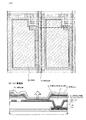
本実施例では、アクティブマトリクス型発光装置全体の外観図について図5に説明する。なお、図5(A)は、発光装置を示す上面図、図5(B)は図5(A)をA−A’で切断した断面図である。点線で示された901はソース信号線駆動回路、902は画素部、903はゲート信号線駆動回路である。また、904は封止基板、905はシール剤であり、シール剤905で囲まれた内側は、シール材(または樹脂)907になっている。
【0114】
なお、908はソース信号線駆動回路901及びゲート信号線駆動回路903に入力される信号を伝送するための配線であり、外部入力端子となるFPC(フレキシブルプリントサーキット)909からビデオ信号やクロック信号を受け取る。なお、ここではFPCしか図示されていないが、このFPCにはプリント配線基盤(PWB)が取り付けられていても良い。本明細書における発光装置には、発光装置本体だけでなく、それにFPCもしくはPWBが取り付けられた状態をも含むものとする。
【0115】
次に、断面構造について図5(B)を用いて説明する。基板910上には駆動回路及び画素部が形成されているが、ここでは、駆動回路としてソース信号線駆動回路901と画素部902が示されている。
【0116】
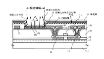
なお、ソース信号線駆動回路901はnチャネル型TFT923とpチャネル型TFT924とを組み合わせたCMOS回路が形成される。また、駆動回路を形成するTFTは、公知のCMOS回路、PMOS回路もしくはNMOS回路で形成しても良い。また、本実施例では、基板上に駆動回路を形成したドライバー一体型を示すが、必ずしもその必要はなく、基板上ではなく外部に形成することもできる。
【0117】
また、画素部902はスイッチング用TFT911と、電流制御用TFT912とそのドレインに電気的に接続された第1の電極(陽極)913を含む複数の画素により形成される。
【0118】
また、第1の電極(陽極)913の両端には隔壁が形成され、隔壁の下層である絶縁膜914の側面は斜面を有している。また、隔壁の上層には実施の形態1に示した光吸収多層膜が設けられており絶縁膜914の形成と同時に形成することが望ましい。外部からの光は、隔壁の上層に設けられた光吸収多層膜により吸収されるため、下方に存在する電極や配線の反射光を抑えることができる。また、光吸収多層膜の一層は、反射性を有する金属膜であり、第2の電極916と接続されて同電位となる。
【0119】
また、第1の電極(陽極)913上には、蒸着マスクを用いた蒸着法、インクジェット法によって有機化合物を含む層915を選択的に形成する。さらに、有機化合物を含む層915上には第2の電極(陰極)916が形成される。これにより、第1の電極(陽極)912、有機化合物を含む層915、及び第2の電極(陰極)916からなる発光素子918が形成される。ここでは発光素子918は白色発光とする例であるので着色層931とBM932からなるカラーフィルター(簡略化のため、ここではオーバーコート層は図示しない)が設けている。
【0120】
また、絶縁層914上には実施例1に示した構成の一部である第3の電極(補助電極)917が形成されており、第2の電極の低抵抗化を実現している。また、第2の電極(陰極)916は全画素に共通の配線としても機能し、第3の電極917および接続配線908を経由してFPC909に電気的に接続されている。
【0121】
また、基板910上に形成された発光素子918を封止するためにシール剤905により封止基板904を貼り合わせる。なお、封止基板904と発光素子918との間隔を確保するために樹脂膜からなるスペーサを設けても良い。そして、シール剤905の内側の空間907にはシール剤(樹脂)が充填されている。なお、シール剤905としてはエポキシ系樹脂を用いるのが好ましい。また、シール剤905はできるだけ水分や酸素を透過しない材料であることが望ましい。
【0122】
また、本実施例では封止基板904を構成する材料としてガラス基板や石英基板の他、FRP(Fiberglass-Reinforced Plastics)、PVF(ポリビニルフロライド)、マイラー、ポリエステルまたはアクリル等からなるプラスチック基板を用いることができる。また、シール剤905を用いて封止基板904を接着した後、さらに側面(露呈面)を覆うようにシール剤で封止することも可能である。
【0123】
以上のようにして発光素子をシール材907に封入することにより、発光素子を外部から完全に遮断することができ、外部から水分や酸素といった有機化合物層の劣化を促す物質が侵入することを防ぐことができる。従って、信頼性の高い発光装置を得ることができる。
【0124】
また、本実施例は実施の形態1乃至3、実施例1と自由に組み合わせることができる。
【0125】
[実施例3]
本実施例では、実施例1とは異なる成膜方法および成膜装置(図9、図10に示す)を用いて有機化合物を含む層、または陰極を形成する例を説明する。なお、第1の電極および隔壁を形成するまでの工程は、実施例1と同一であるため、ここでは説明を省略する。
【0126】
実施例1では、蒸着マスクを用いた蒸着法、またはインクジェット法により有機化合物を含む層や第2の電極を形成する例であったが、本実施例では、減圧下で発光性材料を含む溶液を第1の電極、即ち画素電極(陽極もしくは陰極)に向けて噴射し、前記発光性材料を前記画素電極上に堆積させて発光層を形成することを特徴とするものである。
【0127】
減圧下とは、大気圧よりも低い圧力下であることを指し、窒素、希ガスその他の不活性ガスで充填された雰囲気(以下、不活性雰囲気という。)では1×10²〜2×10⁴Pa(好ましくは、5×10²〜5×10³Pa)とすれば良いし、真空中では1〜5×10⁴Pa(1×10²〜1×10³Pa)とすれば良い。減圧下におくことで、雰囲気中に噴射された液滴は画素電極に到達するまでの間、常に液滴から溶媒が揮発し、その体積は減少していく。そして、画素電極上に到達した時点で殆どすべての溶媒が揮発し、到達と同時に膜形成が完了する。即ち、溶液塗布後に焼成工程等の加熱工程を必要としない点で従来技術よりも優れている。このとき、画素電極が50〜200℃に加熱されていると、付着後も容易に溶媒を揮発させることができるため、さらなる膜質の向上に有効である。
【0128】
また、画素電極に到達する前に十分溶媒を揮発させることが好ましいため、本発明に用いる溶媒は、できるだけ揮発性の高い材料(即ち蒸気圧の高い材料)を用いると良い。なぜならば揮発性が低いと画素電極と溶液の噴射口(ノズルの先端部)との距離を長くして揮発に要する時間を稼ぐ必要があるが、当該距離が長いと液滴の弾道誤差が大きくなるからである。
【0129】
図10(A)は、発光性材料を含む溶液が噴射された直後の状態を表し、図10(B)は、発光性材料が陽極もしくは陰極に到達して薄膜(発光層)が形成された状態を表している。
【0130】
図10(A)において、101は陽極もしくは陰極であり、102は各画素を画定する隔壁、103はキャリア注入層である。キャリア注入層103は、101が陽極であれば正孔注入層であるし、陰極であれば電子注入層である。また、104は溶液を塗布するための装置(以下、溶液塗布装置という。)におけるヘッド部を拡大したものであり、一部分については内部構造を示している。ヘッド部104は、発光性材料を含む溶液を噴射する機能を持つ複数の噴射部105a〜105cを有しており、それぞれに圧電素子(ピエゾ素子)106a〜106cが設けられる。また、噴射部105a〜105cのそれぞれには発光性材料を含む溶液107a〜107cが充填されている。
【0131】
ここで発光性材料を含む溶液107aは、赤色に発光する発光性材料を含み、発光性材料を含む溶液107bは、緑色に発光する発光性材料を含み、発光性材料を含む溶液107cは、青色に発光する発光性材料を含む。これら三種類の発光性材料は、それぞれ赤色に発光する画素、緑色に発光する画素及び青色に発光する画素を構成し、これら三つの画素を一つの画素ユニット(画素単位)として捉える。なお、図10(A)においてはR(赤)、G(緑)、B(青)それぞれ一つに対応する噴射部しか説明していないが、並列に複数の噴射部(ノズル)を並べることも可能であり、スループットを考慮すると画素部の一行分もしくは一列分の画素数(ピクセル数)に相当する数だけ並べることが最も望ましいと言える。
【0132】
また、図10の成膜装置において最も特徴的な点は、ヘッド部104と陽極もしくは陰極101との間の空間108が減圧、即ち大気圧よりも低い圧力に維持されている点にある。具体的には、不活性雰囲気では1×10²〜2×10⁴Pa(好ましくは、5×10²〜5×10³Pa)であり、真空中では1〜5×10⁴Pa(1×10²〜1×10³Pa)である。噴射部105a〜105cに充填された発光性材料を含む溶液107a〜107cは、圧電素子106a〜106cの体積変化により加圧されて押し出され、画素電極101に向かって噴射される。そして、噴射された液滴109は、減圧下で溶媒を揮発させながら進行し、残存した発光性材料が画素電極101上に堆積する。その結果、発光性材料は間欠的に堆積されることになる。
【0133】
こうして堆積された薄膜は、特に加熱等の手段により溶媒を揮発させなくても十分に溶媒成分を除去した状態で薄膜化されているため、脱ガスによる経時劣化等の問題の少ない発光層が得られる。以上のような構成により溶液を塗布した後も焼成工程等を必要とせず、スループットを大幅に向上できると共に、加熱による発光性材料自体の劣化も防ぐことができる。なお、本発明の特徴は焼成工程を必要としない点ではあるが、真空中の加熱処理等の焼成工程を併用しても溶媒成分を十分に除去した脱ガスの少ない発光層が得られるという本発明の効果を損なうものではない。
【0134】
こうして図10(B)に示すように、赤色に発光する発光層110a、緑色に発光する発光層110b及び青色に発光する発光層110cが形成される。この後は、必要に応じてキャリア輸送層、キャリア注入層等を形成した後、第2の電極、即ち対向電極(陽極に対しては陰極、陰極に対しては陽極)を設ければ発光素子が完成する。
【0135】
また、本実施例では、溶液塗布を液滴の噴射により行う例を示したが、特に限定されず、ある程度の粘性を有するゲル状の溶液を塗布してもよい。
【0136】
また、発光体の形成から発光素子の封止までの工程を行うため、本実施例に用いる溶液塗布装置をインライン方式の製造装置に組み合わせた例を図9に示す。なお、図9(A)は上面図、図9(B)は側面図である。
【0137】
図9(A)、(B)において、161は基板の搬入を行うロード室、162は基板の搬出を行うアンロード室、163は正孔注入層を成膜する成膜室、164は発光層を成膜する成膜室、165は電子注入層を成膜する成膜室、166は陰極となる金属膜を成膜する成膜室、167はパッシベーション効果を有する保護膜を成膜する成膜室である。図中の矢印170は、基板160の搬送方向であり、既に処理の終了した基板は点線で表してある。このとき、基板160は立てた状態、即ち表面(被処理面)が重力の方向に対して平行な状態で搬送される。
【0138】
なお、ここでは簡略化のため、図示しないが、基板160上には予め、実施例1に従ってTFT、第1の電極および隔壁などが形成されている。本実施例では、実施例1に従って隔壁まで形成された基板をロード室にセットする。
【0139】
成膜室163〜165のそれぞれは、本実施例の溶液塗布装置であり、内部にはヘッド部163a、164a、165aが設けられている。これらのヘッド部はいずれも図10に示した構成を有し、減圧下で有機化合物もしくは無機化合物を含む溶液の塗布及び薄膜形成が行われる。勿論、基板160を150〜200℃で加熱する機構を備えても良い。また、図9(B)に示す矢印171は、ヘッド部164aの移動方向を示しており、基板160の一端から他端に向かって溶液塗布及び薄膜形成が行われる。
【0140】
さらに、このとき、各成膜室163〜165内には窒素、希ガスその他のフッ化性ガスが紙面に垂直な方向に向かって上から下へ流れており、基板160とヘッド部163a〜165aとの間には不活性ガスによる層流(ラミナーフロー)が形成される。このとき、基板を加熱する代わりに又は併用して、流れる不活性ガスを加熱することもできる。勿論、不活性ガスを導入せずに真空とすることも可能である。
【0141】
また、成膜室166はスパッタ法により陰極となる金属膜を成膜するチャンバーであり、基板160が長方形のターゲット166aの横を通過する間に成膜が行われる。例えば、アルミニウムとリチウムとの合金膜といった周期表の1族もしくは2族に属する元素を含む金属膜を形成することが可能である。ターゲット166aの形状はこれに限定されるものではないが、基板160を縦置きにするメリットとして、線状、長方形状、長楕円形状その他の細長い形状のターゲットを使うことにより高いスループットを確保しつつ装置面積を小さくできるという点が挙げられる。
【0142】
また、成膜室167はスパッタ法(好ましくは高周波スパッタ法)によりパッシベーション効果を有する絶縁膜を成膜するチャンバーであり、基板160が長方形のターゲット167aの横を通過する間に成膜が行われる。例えば、窒化シリコン膜、窒化酸化シリコン膜といった緻密性の高いシリコン化合物膜を形成することが可能である。ターゲット167aの形状はこれに限定されるものではないが、基板160を縦置きにするメリットとして、線状、長方形状、長楕円形状その他の細長い形状のターゲットを使うことにより高いスループットを確保しつつ装置面積を小さくできるという点が挙げられる。
【0143】
なお、図9に示す製造装置の特徴として、溶液塗布と同時に薄膜形成が行われるため焼成工程等が不要である点が挙げられるが、各成膜室163〜166の間において真空中での加熱等の焼成工程を設けても構わない。発光層等の薄膜中から溶媒成分を除去すればその分だけ信頼性が向上すると考えられるからである。
【0144】
また、本実施例は実施の形態1乃至3、実施例1、実施例2と自由に組み合わせることができる。
【0145】
[実施例4]
本発明を実施することによって有機化合物を含む層を発光層とするモジュール(アクティブマトリクス型ELモジュール)を組み込んだ全ての電子機器が完成される。
【0146】
その様な電子機器としては、ビデオカメラ、デジタルカメラ、ヘッドマウントディスプレイ(ゴーグル型ディスプレイ)、カーナビゲーション、プロジェクタ、カーステレオ、パーソナルコンピュータ、携帯情報端末(モバイルコンピュータ、携帯電話または電子書籍等)などが挙げられる。それらの一例を図11、図12に示す。
【0147】
図11(A)はパーソナルコンピュータであり、本体2001、画像入力部2002、表示部2003、キーボード2004等を含む。
【0148】
図11(B)はビデオカメラであり、本体2101、表示部2102、音声入力部2103、操作スイッチ2104、バッテリー2105、受像部2106等を含む。
【0149】
図11(C)はモバイルコンピュータ(モービルコンピュータ)であり、本体2201、カメラ部2202、受像部2203、操作スイッチ2204、表示部2205等を含む。
【0150】
図11(D)はゴーグル型ディスプレイであり、本体2301、表示部2302、アーム部2303等を含む。
【0151】
図11(E)はプログラムを記録した記録媒体(以下、記録媒体と呼ぶ)を用いるプレーヤーであり、本体2401、表示部2402、スピーカ部2403、記録媒体2404、操作スイッチ2405等を含む。なお、このプレーヤーは記録媒体としてDVD(Digtial Versatile Disc)、CD等を用い、音楽鑑賞や映画鑑賞やゲームやインターネットを行うことができる。
【0152】
図11(F)はデジタルカメラであり、本体2501、表示部2502、接眼部2503、操作スイッチ2504、受像部(図示しない)等を含む。
【0153】
図12(A)は携帯電話であり、本体2901、音声出力部2902、音声入力部2903、表示部2904、操作スイッチ2905、アンテナ2906、画像入力部(CCD、イメージセンサ等)2907等を含む。
【0154】
図12(B)は携帯書籍(電子書籍)であり、本体3001、表示部3002、3003、記憶媒体3004、操作スイッチ3005、アンテナ3006等を含む。
【0155】
図12(C)はディスプレイであり、本体3101、支持台3102、表示部3103等を含む。
【0156】
ちなみに図12(C)に示すディスプレイは中小型または大型のもの、例えば5〜20インチの画面サイズのものである。また、このようなサイズの表示部を形成するためには、基板の一辺が1mのものを用い、多面取りを行って量産することが好ましい。中小型または大型のものとする場合、実施例2または実施例3に示した補助電極を形成することが好ましい。
【0157】
以上の様に、本発明の適用範囲は極めて広く、あらゆる分野の電子機器の作製方法に適用することが可能である。また、本実施例の電子機器は実施の形態1乃至3、実施例1、実施例2、実施例3のどのような組み合わせからなる構成を用いても実現することができる。
【0158】
【発明の効果】
本発明により、上面出射型の発光装置において、外光が照射した際、設けられた光吸収多層膜によって、発光領域以外の電極の反射および配線の反射を防止することができる。
【図面の簡単な説明】
【図1】 実施の形態1を示す図。
【図2】 実施例1を示す図。
【図3】 実施の形態3を示す図。
【図4】 実施例1を示す図。
【図5】 実施例2を示す図。
【図6】 実施の形態2を示す図。
【図7】 本発明の光吸収多層膜のシミュレーション結果である。
【図8】 本発明の光吸収多層膜のシミュレーション結果である。
【図9】 製造装置の一例を示す図である。(実施例3)
【図10】 製造装置の一例を示す図である。(実施例3)
【図11】 電子機器の一例を示す図。(実施例4)
【図12】 電子機器の一例を示す図。(実施例4)[0001]
BACKGROUND OF THE INVENTION
The present invention relates to a light-emitting device using a light-emitting element in which fluorescence or phosphorescence is obtained by applying an electric field to an element in which a film containing an organic compound (hereinafter referred to as an “organic compound layer”) is provided between a pair of electrodes. It relates to a manufacturing method thereof. Note that a light-emitting device in this specification refers to an image display device, a light-emitting device, or a light source (including a lighting device). Also, a module in which a connector such as an FPC (Flexible printed circuit) or TAB (Tape Automated Bonding) tape or TCP (Tape Carrier Package) is attached to the light emitting device, or a module in which a printed wiring board is provided at the end of the TAB tape or TCP In addition, a module in which an IC (integrated circuit) is directly mounted on a light emitting element by a COG (Chip On Glass) method is also included in the light emitting device.
[0002]
Note that in this specification, a semiconductor device refers to all devices that can function by utilizing semiconductor characteristics, and an electro-optical device, a semiconductor circuit, and an electronic device are all semiconductor devices.
[0003]
[Prior art]
A light-emitting element using an organic compound having characteristics such as thin and light weight, high-speed response, and direct current low-voltage driving as a light emitter is expected to be applied to a next-generation flat panel display. In particular, a display device in which light emitting elements are arranged in a matrix is considered to be superior to a conventional liquid crystal display device in that it has a wide viewing angle and excellent visibility.
[0004]
The light-emitting mechanism of the light-emitting element recombines electrons injected from the cathode and holes injected from the anode at the emission center in the organic compound layer by applying a voltage with the organic compound layer sandwiched between a pair of electrodes. Thus, it is said that molecular excitons are formed, and when the molecular excitons return to the ground state, energy is emitted and light is emitted. Singlet excitation and triplet excitation are known as excited states, and light emission is considered to be possible through either excited state.
[0005]
For a light-emitting device formed by arranging such light-emitting elements in a matrix, driving methods such as passive matrix driving (simple matrix type) and active matrix driving (active matrix type) can be used. However, when the pixel density increases, the active matrix type in which a switch is provided for each pixel (or one dot) is considered to be advantageous because it can be driven at a lower voltage.
[0006]
In addition, organic compounds that can be said to be the center of the light-emitting element, ie, the organic compound layer (specifically, the light-emitting layer), are researched on low-molecular materials and high-molecular (polymer-based) materials. Attention has been focused on polymer materials that are easier to handle and have higher heat resistance.
[0007]
In addition, in a conventional light emitting device, a light emitting element in which an electrode electrically connected to a TFT on a substrate is formed as an anode, an organic compound layer is formed on the anode, and a cathode is formed on the organic compound layer. It has a structure in which light generated in the organic compound layer is extracted from the anode, which is a transparent electrode, toward the TFT. In this structure, when the resolution is improved, there arises a problem that the aperture ratio is limited by the arrangement of TFTs and wirings in the pixel portion.
[0008]
On the other hand, there is a structure in which an electrode is formed as an anode, a layer containing an organic compound is formed on the anode, and a cathode that is a transparent electrode is formed on the layer containing the organic compound (hereinafter referred to as a top emission structure). .
[0009]
[Problems to be solved by the invention]
In the top emission structure, wiring and TFTs are provided in places other than the light emitting region that emits light, and there is a problem that reflected light from the wiring reaches the eyes of the observer.
[0010]
It is an object of the present invention to provide a light emitting device having a structure that can solve the above problems and a method for manufacturing the light emitting device.
[0011]
[Means for Solving the Problems]
The present invention has a structure in which a multilayer film that absorbs light is provided in a region other than the light emitting region to prevent light reflected by the wiring from reaching the eyes of the observer. Specifically, a multilayer film that absorbs light is used as an upper layer of a partition wall (also referred to as a bank or a barrier) that covers an end portion of the first electrode, and an organic resin is used as a lower layer. In the present invention, the partition wall is formed of a laminate of three or more layers of different materials.
[0012]
In order to form a multilayer film that absorbs light, for example, a silicon nitride film and a metal nitride film (typically, a metal film having a high reflectance (typically, a metal film mainly containing aluminum or silver) are formed. (E.g., a titanium nitride film, a tantalum nitride film, etc.) and a silicon nitride film may be laminated with an appropriate film thickness. When light is incident from the outside, optical interference caused between these layers Decrease by absorption. Note that the portion where the multilayer film that absorbs light is provided does not overlap the light emitting region.
[0013]
In addition, since the multilayer film that absorbs light arranged above the TFT can prevent irradiation from outside light, deterioration due to irradiation of the TFT with outside light can also be prevented.
[0014]
The configuration of the invention disclosed in this specification is as follows.
A first electrode connected to a thin film transistor over a substrate having an insulating surface;
A partition wall covering an end of the first electrode;
A light-emitting element having a layer containing an organic compound in contact with the first electrode and a second electrode in contact with the layer,
The partition wall is a light emitting device comprising a laminate of an organic resin film and a multilayer film that absorbs light.
[0015]
In the above structure, the partition wall covers a region other than the light-emitting region where the first electrode and the layer containing an organic compound are in contact with each other. Note that the partition wall is not formed at a portion where the second electrode is connected to the lower wiring or a terminal portion where the FPC is connected. When the drive circuit is also formed over the same substrate, the same stack as the partition covering the drive circuit may be provided, or may not be provided. At least the partition wall covers a region other than the light emitting region serving as a display region in the pixel portion.
[0016]
In each of the above structures, the multilayer film provided over the partition includes at least one nitride insulating film having a light-transmitting property. Specifically, the multilayer film provided on the upper layer of the partition wall includes four layers of a reflective metal film, a translucent film, a film that partially absorbs light, and a translucent film. As a film having at least a structure and having translucency, Al 2 O Three , SiO 2 , ZrO 2 , HfO 2 , Sc 2 O Three TiO 2 , ITO, or ZnO is a film including at least one layer.
[0017]
Alternatively, in each of the above structures, the multilayer film provided over the reflective metal film may be a multilayer film including at least one light-transmitting nitride insulating film. When a film including aluminum as a main component, a silicon nitride film, a titanium nitride film, and a silicon nitride film is used, the reflectance can be reduced to 5% or less. Further, when a nitride insulating film or a metal nitride film is used as the multilayer film, it can function as a blocking layer for oxygen or moisture, so that deterioration of the EL element can be suppressed. The same effect can be obtained by using a brown or black metal film such as a tantalum nitride film instead of titanium nitride.
[0018]
In each of the above configurations, other films that partially absorb light include Al, Cu, Au, Mo, Ni, Pt, Rh, Ag, W, Cr, Co, Si, Zr, Ta, Inconel, or A film including at least one layer of nichrome may be used.
[0019]
In each of the above structures, the second electrode is a conductive film that transmits light, such as a thin metal film, a transparent conductive film, or a stacked layer thereof.
[0020]
In each of the above structures, the layer containing the organic compound is a material that emits white light, and is combined with a color filter provided in a sealing material, or the layer containing the organic compound is A light emitting device which is a material emitting monochromatic light and combined with a color conversion layer or a colored layer provided on a sealing material. In addition, a layer containing different organic compounds may be selectively formed for each pixel so that RGB light emission can be obtained. In that case, a color filter is not particularly necessary.
[0021]
In each of the above structures, the first electrode is an anode, and the second electrode is a cathode. Alternatively, each of the above structures is characterized in that the first electrode is a cathode and the second electrode is an anode.
[0022]
Further, according to the present invention, a wiring (also referred to as an auxiliary wiring or a third electrode) is formed on a partition wall disposed between each pixel electrode by a vapor deposition method using a vapor deposition mask, and serves as a cathode (an electrode that transmits light). The film resistance may be reduced. It is also a feature of the present invention that a lead-out wiring is formed using the auxiliary wiring and is connected to another wiring existing in the lower layer.
[0023]
In each of the above structures, the first electrode may have a concave shape. If the barrier ribs are formed in a self-alignment manner using the mask, the number of masks is not increased in forming the first electrode shape. The step portion of the first electrode (upper end portion of the inclined portion) and the side surface of the insulator are made to substantially coincide with each other, and from the viewpoint of step coverage, the inclination angle and the insulator on the inclined surface of the first electrode are preferable. It is desirable that the inclination angle on the side surface of the same is the same. The step at the end portion of the first electrode can prevent light emitted from the light emitting element (including light emitted in the lateral direction) from reaching the TFT. When the first electrode has a concave shape, the first electrode has an inclined surface toward the center of the first electrode, and an inclination angle (also referred to as a taper angle) is 50 °. More than, less than 60 °, more preferably 54.7 °. The light reflected by the inclined surface of the first electrode is appropriately dispersed so that the light is not dispersed between the layers or becomes stray light, the material of the organic compound layer and the film thickness, or the material of the second electrode and It is necessary to set the film thickness.
[0024]
In addition, the configuration of the invention for realizing the above configurations is as follows.
A method for manufacturing a light emitting device having a light emitting element having an anode, a layer containing an organic compound in contact with the anode, and a cathode in contact with the layer containing the organic compound,
Forming a stack of an insulating film and a multilayer film that absorbs light on the first electrode made of a metal film;
Selectively etching a stack of the insulating film and a multilayer film that absorbs light to form a partition wall that covers an end of the first electrode;
Forming a film containing an organic compound;
And a step of forming a second electrode made of a metal thin film that transmits light over a film containing the organic compound.
[0025]
In the structure related to the manufacturing method, the insulating film is made of an inorganic insulating film or an organic resin film.
[0026]
In the structure related to the above manufacturing method, the first electrode is an anode and is formed of a metal layer having a work function larger than that of the second electrode.
[0027]
In the structure related to the manufacturing method, the multilayer film that absorbs light includes at least one metal film having reflectivity.
[0028]
Further, in the structure related to the manufacturing method, the multilayer film that absorbs light is made of Al. 2 O Three , SiO 2 , ZrO 2 , HfO 2 , Sc 2 O Three TiO 2 It is characterized by including at least one layer made of ITO, ZnO.
[0029]
In the structure related to the manufacturing method, the multilayer film that absorbs light includes at least one nitride insulating film having a light-transmitting property.
[0030]
In the configuration related to the manufacturing method, the multilayer film that absorbs light includes Ti, Al, Cu, Au, Mo, Ni, Pt, Rh, Ag, W, Cr, Co, Si, Zr, Ta, Inconel, Alternatively, it includes at least one layer made of nichrome.
[0031]
Note that the EL element includes a layer containing an organic compound (hereinafter, referred to as an EL layer) from which luminescence generated by applying an electric field is obtained, an anode, and a cathode. Luminescence in an organic compound includes light emission (fluorescence) when returning from the singlet excited state to the ground state and light emission (phosphorescence) when returning from the triplet excited state to the ground state. A light-emitting device manufactured by a film formation method can be applied to either light emission.
[0032]
A light-emitting element having an EL layer (EL element) has a structure in which the EL layer is sandwiched between a pair of electrodes. The EL layer usually has a stacked structure. A typical example is a “hole transport layer / light emitting layer / electron transport layer” stacked structure proposed by Tang et al. Of Kodak Eastman Company. This structure has very high luminous efficiency, and most of the light emitting devices that are currently under research and development employ this structure.
[0033]
In addition, a hole injection layer / a hole transport layer / a light emitting layer / an electron transport layer, or a hole injection layer / a hole transport layer / a light emitting layer / an electron transport layer / an electron injection layer are sequentially laminated on the anode. Good structure. You may dope a fluorescent pigment | dye etc. with respect to a light emitting layer. These layers may all be formed using a low molecular material, may be formed using a high molecular material, or may be an inorganic material layer. Note that in this specification, all layers provided between a cathode and an anode are collectively referred to as an EL layer. Therefore, the hole injection layer, the hole transport layer, the light emitting layer, the electron transport layer, and the electron injection layer are all included in the EL layer.
[0034]
In the light emitting device of the present invention, the screen display driving method is not particularly limited, and for example, a dot sequential driving method, a line sequential driving method, a surface sequential driving method, or the like may be used. Typically, a line sequential driving method is used, and a time-division gray scale driving method or an area gray scale driving method may be used as appropriate. The video signal input to the source line of the light-emitting device may be an analog signal or a digital signal, and a drive circuit or the like may be designed in accordance with the video signal as appropriate.
[0035]
DETAILED DESCRIPTION OF THE INVENTION
Embodiments of the present invention will be described below.
[0036]
A cross-sectional view (a part of one pixel) of the active matrix light-emitting device is shown in FIG. Here, a light-emitting element using a layer containing an organic compound made of a polymer material that emits white light as a light-emitting layer will be described as an example.
[0037]
In FIG. 1A, a TFT (p-channel TFT) provided on a
[0038]
[0039]
The power supply line 17 is also formed with the same stacked structure as the first electrode. Further, the
[0040]
Further, in order to obtain white light emission, a poly (ethylenedioxythiophene) / poly (styrenesulfonic acid) aqueous solution (PEDOT / PSS) acting as a hole injection layer was applied and fired as the layer 20 containing an organic compound over the entire surface. Later, a luminescent center dye (1,1,4,4-tetraphenyl-1,3-butadiene (TPB), 4-dicyanomethylene-2-methyl-6- (p-dimethylamino-styryl) acting as a luminescent layer -4H-pyran (DCM1), Nile Red,
[0041]
It is also possible to obtain white light emission as a whole by appropriately selecting a film containing an organic compound that emits red light, a film containing an organic compound that emits green light, or a film containing an organic compound that emits blue light, and mixing them in layers. .
[0042]
21 as CaF 2 After forming the
[0043]
When the Al film is used for the second electrode 21, the material in contact with the layer 20 containing an organic compound can be formed of a material other than an oxide, and the reliability of the light-emitting device can be improved. Instead of the Al film, a transparent conductive film (ITO (indium oxide tin oxide alloy), indium zinc oxide alloy (In 2 O Three -ZnO), zinc oxide (ZnO) or the like may be used. CaF 2 Alternatively, a thin metal layer (typically an alloy such as MgAg, MgIn, or AlLi) may be used.
[0044]
Further, both end portions of the first electrode 18 and the space between them are covered with a partition wall (also called a barrier or a bank). In the present invention, the partition has a function of insulating between the electrodes and absorbing outside light. As a partition, the lower layer is an insulating film 19 (inorganic insulating film or organic insulating film), and the upper layer is a multilayer film 24 that absorbs light (also referred to as a light-absorbing multilayer film), typically a reflective metal film and A four-layer structure in which a light-transmitting film, a film that partially absorbs light, and a light-transmitting film are stacked in this order may be used. In FIG. 1, for the sake of simplicity, the multilayer film 24 that absorbs light is shown as a single layer, but actually, at least four or more layers are stacked.
[0045]
A film containing Al or Ag as a main component is used as the reflective metal film. In addition, as a light-transmitting film, Al 2 O Three , SiO 2 , ZrO 2 , HfO 2 , Sc 2 O Three TiO 2 , ITO, or ZnO, and other films that partially absorb light include Al, Cu, Au, Mo, Ni, Pt, Rh, Ag, W, Cr, Co, Si, A layer made of Zr, Ta, inconel, or nichrome may be used.
[0046]
In order to form a layer containing an organic compound later, a multilayer film that absorbs light from the outside with a film containing nitrogen is described here. The following simulation was performed.
[0047]
A silicon nitride film (film thickness: 37 nm) obtained by sputtering using a silicon target in an atmosphere containing nitrogen and argon on a film containing aluminum as a main component (film thickness: 100 nm), which is a reflective metal film; Results of obtaining reflectance in a model structure in which a titanium nitride film (film thickness 66 nm) and a silicon nitride film (film thickness 37 nm) obtained by sputtering using a silicon target in an atmosphere containing nitrogen and argon are sequentially stacked. Is FIG. In the wavelength range of 300 nm to 800 nm, the silicon nitride film has a refractive index of 2.04 to 2.2, titanium nitride has a refractive index of 1.67 to 2.35, and aluminum has a refractive index of 0.39 to 1.985. Is going. In the visible region, the average reflectance was 3%. The film thickness is not particularly limited and may be set as appropriate. The optimum film thickness varies depending on the material.
[0048]
Further, FIG. 8 shows a result obtained by performing the same simulation even when the conductive film 21 is covered with the sealing material. Although the reflectance is slightly higher than in FIG. 7, the average can be 6%. When covered with a sealing material, the optimum silicon nitride film thickness was 42 nm.
[0049]
Although an example in which a silicon nitride film, a titanium nitride film, and a silicon nitride film are stacked in this order on a reflective metal film is shown here, for example, a silicon nitride film and a nitride film are formed on a reflective metal film. A tantalum film and a silicon nitride film may be stacked in this order, or a silicon nitride film, a titanium nitride film, and an ITO film may be stacked on the reflective metal film. It is preferable to stack a silicon nitride film, a titanium nitride film, and an ITO film in this order on a reflective metal film because a process margin for subsequent etching is large.
[0050]
In addition, all of these multilayer films can be formed by a sputtering method, and an insulating film and a light absorption layer can be continuously formed without being exposed to the air. Further, if a nitride film is used as the light absorption layer 24, it also functions as a passivation film. Further, when a nitride film is used as the light absorption layer 24, moisture and oxygen can be blocked, which is suitable for a light-emitting element using a layer containing an organic compound.
[0051]
In order to improve the coverage of the organic compound-containing layer 20 and the conductive film 21, the total thickness of the partition walls is preferably thin, and the side walls are also preferably tapered. Note that one layer of the light-absorbing multilayer film is a reflective metal film, which is connected to the second electrode 21 and has the same potential although not shown here.
[0052]
As shown in FIG. 1B, an auxiliary electrode 23 may be provided over the conductive film 21 in order to reduce the resistance of the conductive film (cathode) 21. The auxiliary electrode 23 may be selectively formed by a vapor deposition method using a vapor deposition mask.
[0053]
Although not shown, it is preferable to form a protective film over the second electrode 21 in order to increase the reliability of the light-emitting device. This protective film is an insulating film mainly containing silicon nitride or silicon nitride oxide obtained by sputtering (DC method or RF method), or a thin film mainly containing carbon. If a silicon target is used and formed in an atmosphere containing nitrogen and argon, a silicon nitride film can be obtained. A silicon nitride target may be used. Further, the protective film may be formed using a film forming apparatus using remote plasma. Further, in order to allow light emission to pass through the protective film, it is preferable to make the protective film as thin as possible. In addition, when using the material which has aluminum as a main component as a cathode, the blocking property with respect to oxygen and a water | moisture content is high.
[0054]
In the present invention, the carbon-based thin film is a DLC film (Diamond like Carbon) having a thickness of 3 to 50 nm. DLC films are short-range ordered as bonds between carbons, SP Three Although it has a bond, it has an amorphous structure macroscopically. The composition of the DLC film is 70 to 95 atomic% for carbon and 5 to 30 atomic% for hydrogen, and is very hard and excellent in insulation. Such a DLC film is also characterized by low gas permeability such as water vapor and oxygen. It is also known to have a hardness of 15 to 25 GPa as measured by a microhardness meter.
[0055]
The DLC film can be formed by a plasma CVD method (typically, an RF plasma CVD method, a microwave CVD method, an electron cyclotron resonance (ECR) CVD method, etc.), a sputtering method, or the like. Whichever film formation method is used, the DLC film can be formed with good adhesion. The DLC film is formed by placing the substrate on the cathode. Alternatively, a dense and hard film can be formed by applying a negative bias and utilizing ion bombardment to some extent.
[0056]
The reaction gas used for film formation includes hydrogen gas and hydrocarbon-based gas (for example, CH Four , C 2 H 2 , C 6 H 6 And the like, and ionized by glow discharge, and the ions are accelerated and collided with a negative self-biased cathode to form a film. By doing so, a dense and smooth DLC film can be obtained. The DLC film is an insulating film that is transparent or translucent to visible light.
[0057]
In the present specification, transparent to visible light means that the visible light transmittance is 80 to 100%, and translucent to visible light is a visible light transmittance of 50 to 80%. Refers to that.
[0058]
Although not shown here, the substrate is finally sealed with a substrate for sealing the EL element and a sealing material. A sealing substrate is attached so that an interval of about 2 to 30 μm is maintained, and all the light emitting elements are sealed. It is preferable to perform deaeration by annealing in vacuum immediately before attaching the sealing substrate with a sealing material. It is preferable that all the light emitting elements are sealed so as to cover the entire surface with a sealant and a desiccant is not used. Note that when a space is provided between the substrates and the sealing substrate is attached, a concave portion is provided in the sealing substrate by a sandblast method or the like, and a desiccant is formed in the concave portion in an atmosphere containing an inert gas (rare gas or nitrogen). It is preferable to arrange and bond.
[0059]
Although the top gate type TFT has been described as an example here, the present invention can be applied regardless of the TFT structure. For example, it can be applied to a bottom gate type (reverse stagger type) TFT or a forward stagger type TFT. Is possible.
[0060]
(Embodiment 2)
A method of combining a white light emitting element and a color filter (hereinafter referred to as a color filter method) will be described below with reference to FIG.
[0061]
The color filter method is a method in which red light, green light, and blue light emission are obtained by forming a light emitting element having an organic compound film that emits white light and passing the obtained white light through a color filter.
[0062]
There are various methods for obtaining white light emission. Here, a case where a light emitting layer made of a polymer material that can be formed by coating is used will be described. In this case, the dye doping of the polymer material to be the light emitting layer can be performed by adjusting the solution, and can be obtained extremely easily as compared with the vapor deposition method in which co-evaporation in which a plurality of dyes are doped is performed.
[0063]
Specifically, poly (ethylenedioxythiophene) / poly (styrenesulfone) acting as a hole injection layer on an anode made of a metal (Pt, Cr, W, Ni, Zn, Sn, In) having a high work function. Acid) Aqueous solution (PEDOT / PSS) is applied over the entire surface and baked, and then a luminescent center dye (1,1,4,4-tetraphenyl-1,3-butadiene (TPB), 4-dicyanomethylene acting as a luminescent layer -2-methyl-6- (p-dimethylamino-styryl) -4H-pyran (DCM1), Nile Red,
[0064]
Moreover, although the example which made the organic compound layer laminated | stacked was shown in the said example, an organic compound layer can also be made into a single layer. For example, an electron transporting 1,3,4-oxadiazole derivative (PBD) may be dispersed in hole transporting polyvinyl carbazole (PVK). Further, white light emission can be obtained by dispersing 30 wt% PBD as an electron transporting agent and dispersing an appropriate amount of four kinds of dyes (TPB,
[0065]
The organic compound film is formed between the anode and the cathode, and the holes injected from the anode and the electrons injected from the cathode are recombined in the organic compound film, so that the organic compound film emits white light. Is obtained.
[0066]
It is also possible to obtain white light emission as a whole by appropriately selecting an organic compound film emitting red light, an organic compound film emitting green light, or an organic compound film emitting blue light and mixing them in layers.
[0067]
The organic compound film formed as described above can obtain white light emission as a whole.
[0068]
A color provided with a colored layer (R) that absorbs light other than red light, a colored layer (G) that absorbs light other than green light, and a colored layer (B) that absorbs light other than blue light in the direction in which the organic compound film emits white light. By forming the filter, white light emission from the light emitting element can be separated and obtained as red light emission, green light emission, and blue light emission. In the case of the active matrix type, a TFT is formed between the substrate and the color filter.
[0069]
In addition, the colored layer (R, G, B) can use a simplest stripe pattern, an oblique mosaic arrangement, a triangular mosaic arrangement, an RGBG four-pixel arrangement, or an RGBW four-pixel arrangement.
[0070]
The colored layer constituting the color filter is formed using a color resist made of an organic photosensitive material in which a pigment is dispersed. The chromaticity coordinates of white light emission are (x, y) = (0.34, 0.35). By combining white light emission and a color filter, sufficient color reproducibility as a full color can be ensured.
[0071]
In this case, even if the luminescent color obtained is different, all the organic compound films exhibiting white luminescence are formed, so that it is not necessary to separately form the organic compound film for each luminescent color. Further, a circularly polarizing plate that prevents specular reflection can be omitted.
[0072]
Next, a CCM method (color changing mediums) realized by combining a blue light emitting element having a blue light emitting organic compound film and a fluorescent color conversion layer will be described with reference to FIG.
[0073]
In the CCM method, blue light emitted from a blue light emitting element excites a fluorescent color conversion layer, and color conversion is performed in each color conversion layer. Specifically, the color conversion layer converts blue to red (B → R), the color conversion layer converts blue to green (B → G), and the color conversion layer converts blue to blue (B → B). ) (Note that the conversion from blue to blue is not necessary) to obtain red, green and blue light emission. Also in the case of the CCM method, the active matrix type has a structure in which TFTs are formed between the substrate and the color conversion layer.
[0074]
In this case, it is not necessary to form the organic compound film separately. Further, a circularly polarizing plate that prevents specular reflection can be omitted.
[0075]
Further, when the CCM method is used, since the color conversion layer is fluorescent, it is excited by external light and has a problem of lowering the contrast. Therefore, a color filter is attached as shown in FIG. To increase the contrast.
[0076]
Further, this embodiment mode can be combined with
[0077]
(Embodiment 3)
Here, another structural example will be described with reference to FIG. Since FIG. 3 is the same as FIG. 1 except for a part thereof, the same reference numerals are used for the same portions.
[0078]
In FIG. 3, the wiring has a four-layer structure, a titanium film as 18a, a titanium nitride film as 18b, a film containing aluminum as a main component as 18c, and a titanium nitride film as 18d are stacked in this order and are in contact with the layer 20 containing an organic compound. 18b functions as an anode. The power supply line 17 is also formed with the same laminated structure. The stacked structure includes a film containing aluminum as a main component, can be a low-resistance wiring, and the
[0079]
As a manufacturing process, a first electrode made of a metal film is formed, a partition wall that covers an end portion of the first electrode is formed, and etching is performed in a self-aligning manner using the partition wall as a mask. The portion is etched and the central portion of the first electrode is thinly etched to form a step at the end. By this etching, the central portion of the first electrode is made thin and flat, and the end portion of the first electrode covered with the partition wall has a thick shape, that is, a concave shape. The structure shown in FIG. 3 prevents stray light and reflects or collects light emitted in the lateral direction on the slope formed on the step portion of the first electrode, and passes through one direction (the second electrode). Direction) to increase the amount of emitted light.
[0080]
Accordingly, the sloped
[0081]
Further, this embodiment can be freely combined with
[0082]
The present invention having the above-described configuration will be described in more detail with the following examples.
[0083]
(Example)
[Example 1]
In this embodiment, an example of a procedure for forming a light emitting element of the present invention will be briefly described below with reference to FIG.
[0084]
First, a base insulating film is formed over a substrate having an insulating surface.
[0085]
The base insulating film uses a plasma CVD method as the first layer, and SiH Four , NH Three And N 2 A silicon oxynitride film formed using O as a reaction gas is formed to a thickness of 10 to 200 nm (preferably 50 to 100 nm). Here, a silicon oxynitride film (composition ratio: Si = 32%, O = 27%, N = 24%, H = 17%) with a thickness of 50 nm is formed. Next, as the second layer of the base insulating film, a plasma CVD method is used, and SiH Four And N 2 A silicon oxynitride film formed using O as a reaction gas is formed to a thickness of 50 to 200 nm (preferably 100 to 150 nm). Here, a 100-nm-thick silicon oxynitride film (composition ratio Si = 32%, O = 59%, N = 7%, H = 2%) is formed. In this embodiment, a two-layer structure is used as the base insulating film, but a single layer film of the insulating film or a structure in which two or more layers are stacked may be used.
[0086]
Next, a semiconductor layer is formed over the base film. The semiconductor layer which becomes the active layer of the TFT is formed by forming a semiconductor film having an amorphous structure by a known means (sputtering method, LPCVD method, plasma CVD method, etc.) and then a known crystallization treatment (laser crystallization). A crystalline semiconductor film obtained by performing a method, a thermal crystallization method, or a thermal crystallization method using a catalyst such as nickel) is formed into a desired shape by patterning. The semiconductor layer is formed with a thickness of 25 to 80 nm (preferably 30 to 60 nm). There is no limitation on the material of the crystalline semiconductor film, but it is preferably formed of silicon or a silicon germanium alloy.
[0087]
When a crystalline semiconductor film is formed by laser crystallization, a pulse oscillation type or continuous emission type excimer laser, YAG laser, YVO Four A laser can be used. When these lasers are used, it is preferable to use a method in which laser light emitted from a laser oscillator is linearly collected by an optical system and irradiated onto a semiconductor film. Crystallization conditions are appropriately selected by the practitioner. When an excimer laser is used, the pulse oscillation frequency is 30 Hz and the laser energy density is 100 to 400 mJ / cm. 2 (Typically 200-300mJ / cm 2 ). When a YAG laser is used, the second harmonic is used and the pulse oscillation frequency is 1 to 10 kHz, and the laser energy density is 300 to 600 mJ / cm. 2 (Typically 350-500mJ / cm 2 ) Then, when the laser beam condensed linearly with a width of 100 to 1000 μm, for example, 400 μm is irradiated over the entire surface of the substrate, the superposition ratio (overlap ratio) of the linear laser light at this time is 80 to 98%. Good.
[0088]
Next, the surface of the semiconductor layer is washed with an etchant containing hydrofluoric acid to form a
[0089]
Next, after cleaning the surface of the
[0090]
Next, an impurity element imparting p-type conductivity to the semiconductor (such as B), here boron, is added as appropriate, so that the source region and the
[0091]
In the subsequent steps, an
[0092]
In this embodiment, a p-channel TFT is used. However, it goes without saying that a p-channel TFT can be formed by using an n-type impurity element (P, As, etc.) instead of a p-type impurity element. Yes.
[0093]
In this embodiment, the top gate type TFT is described as an example. However, the present invention can be applied regardless of the TFT structure. For example, the present invention can be applied to a bottom gate type (reverse stagger type) TFT or a forward stagger type TFT. Is possible.
[0094]
Through the above steps, a TFT (only the
[0095]
In this embodiment, the first electrodes 66a and 66b are made of Ti, TiN, TiSi. X N Y , Ni, W, WSi X , WN X , WSi X N Y , Ta, TaN X , TaSi X N Y An element selected from NbN, Mo, Cr, Pt, Zn, Sn, In, or Mo, or an alloy material or a compound material containing the element as a main component, or a laminated film of them as a total film What is necessary is just to use in the range of thickness 100nm -800nm.
[0096]
In particular, the first electrode 66a in contact with the
[0097]
The first electrodes 66a and 66b can be formed at the same time as other wirings, for example, the source wiring 64 and the power supply line.
[0098]
Next, a partition wall (called a bank, a barrier, a bank, or the like) is formed to cover the end portion of the first electrode (and the contact portion with the drain region 62). The etching for forming the shape of the partition wall may be performed once or a plurality of times by dry etching or wet etching. It is also important to select a material for the partition so as to ensure a sufficient selection ratio when performing etching for forming the shape of the partition. Note that a light absorption multilayer film 61 is provided on the upper layer of the partition wall to absorb external light.
[0099]
As the
[0100]
Next, an auxiliary electrode 60 is formed in order to lower the electric resistance of a thin conductive film to be formed later. The auxiliary electrode 60 may be formed by patterning a metal film obtained by a sputtering method, or by an evaporation method using an evaporation mask. In the present embodiment, an example in which the auxiliary electrode 60 is arranged in the Y direction as shown in FIG. 2A is shown, but there is no particular limitation, and the auxiliary electrode may be arranged in the X direction.
[0101]
FIG. 4 shows an external view of a panel in which auxiliary electrodes are arranged in the X direction. The auxiliary electrode (auxiliary wiring) 70 is routed as shown in FIG. 4 and is formed so as to be in contact with the
[0102]
Next, a layer 68 containing an organic compound is formed by a vapor deposition method or a coating method (inkjet method or the like). For example, when the vapor deposition method is used, the degree of vacuum is 5 × 10. -3 Torr (0.665 Pa) or less, preferably 10 -Four -10 -6 Vapor deposition is performed in a deposition chamber evacuated to Pa. At the time of vapor deposition, the organic compound is vaporized by resistance heating in advance, and is scattered in the direction of the substrate by opening the shutter at the time of vapor deposition. The vaporized organic compound scatters upward and is deposited on the substrate through an opening provided in the metal mask. By laminating by vapor deposition, a layer containing an organic compound showing white as the whole light emitting element is formed.
[0103]
For example, Alq Three , Alq partially doped with Nile Red, a red luminescent dye Three , Alq Three , P-EtTAZ, and TPD (aromatic diamine) are sequentially laminated to obtain a white color.
[0104]
Moreover, when forming the layer containing an organic compound by the apply | coating method using spin coating, after apply | coating, it is preferable to bake by vacuum heating. For example, a poly (ethylenedioxythiophene) / poly (styrenesulfonic acid) aqueous solution (PEDOT / PSS) that acts as a hole injection layer is applied and fired on the entire surface, and then a luminescent center dye (1, 1,4,4-tetraphenyl-1,3-butadiene (TPB), 4-dicyanomethylene-2-methyl-6- (p-dimethylamino-styryl) -4H-pyran (DCM1), Nile Red,
[0105]
In the above example, the organic compound layer 68 is stacked, but the organic compound layer may be a single layer. For example, an electron transporting 1,3,4-oxadiazole derivative (PBD) may be dispersed in hole transporting polyvinyl carbazole (PVK). Further, white light emission can be obtained by dispersing 30 wt% PBD as an electron transporting agent and dispersing an appropriate amount of four kinds of dyes (TPB,
[0106]
Next, a metal having a small work function (MgAg, MgIn, AlLi, CaF 2 , An alloy such as CaN, or a film formed by co-evaporation of an element belonging to
[0107]
The light-emitting element thus obtained emits white light in the direction of the arrow in FIG. Moreover, since external light is absorbed by the light absorption multilayer film 61 provided on the upper layer of the partition wall, reflected light from the electrodes and wirings can be suppressed.
[0108]
After the formation up to the second electrode (conductive film) through the above steps, a sealing substrate (transparent substrate) is bonded with a sealant to seal the light emitting element formed over the substrate. Note that a spacer made of a resin film may be provided in order to ensure a space between the sealing substrate and the light emitting element. The space inside the sealing agent is filled with an inert gas such as nitrogen. In addition, it is preferable to use an epoxy resin as the sealing agent. Further, it is desirable that the sealant is a material that does not transmit moisture and oxygen as much as possible. Furthermore, a substance (such as a desiccant) having an effect of absorbing oxygen and water may be included in the space. Moreover, instead of filling the space inside the sealing agent with gas, a sealing material may be filled.
[0109]
By encapsulating the light emitting element in the space as described above, the light emitting element can be completely blocked from the outside, and can prevent the entry of substances that promote deterioration of the organic compound layer such as moisture and oxygen from the outside. it can. Therefore, a highly reliable light-emitting device can be obtained.
[0110]
In addition, since the auxiliary electrode 60, 70 is formed in this embodiment to reduce the resistance of the cathode, it can be applied to a pixel portion having a large size.
[0111]
In this embodiment, the example in which the layer containing the organic compound is formed after the auxiliary electrode 60 is formed is shown. However, the order of formation is not particularly limited, and the auxiliary electrode is formed after the layer 68 containing the organic compound is formed. 60 may be formed.
[0112]
In addition, this embodiment can be freely combined with any one of
[0113]
[Example 2]
In this embodiment, an external view of the entire active matrix light emitting device will be described with reference to FIG. 5A is a top view illustrating the light-emitting device, and FIG. 5B is a cross-sectional view taken along line AA ′ in FIG. 5A. Reference numeral 901 indicated by a dotted line denotes a source signal line driver circuit, 902 denotes a pixel portion, and 903 denotes a gate signal line driver circuit. Reference numeral 904 denotes a sealing substrate,
[0114]
Note that reference numeral 908 denotes wiring for transmitting signals input to the source signal line driver circuit 901 and the gate signal line driver circuit 903, and a video signal and a clock signal are received from an FPC (flexible printed circuit) 909 serving as an external input terminal. receive. Although only the FPC is shown here, a printed wiring board (PWB) may be attached to the FPC. The light-emitting device in this specification includes not only a light-emitting device body but also a state in which an FPC or a PWB is attached thereto.
[0115]
Next, a cross-sectional structure is described with reference to FIG. A driver circuit and a pixel portion are formed over the substrate 910. Here, a source signal line driver circuit 901 and a pixel portion 902 are shown as the driver circuits.
[0116]
Note that as the source signal line driver circuit 901, a CMOS circuit in which an n-channel TFT 923 and a p-
[0117]
The pixel portion 902 is formed by a plurality of pixels including a switching
[0118]
In addition, partition walls are formed at both ends of the first electrode (anode) 913, and a side surface of the insulating film 914 which is a lower layer of the partition wall has a slope. In addition, the light absorption multilayer film described in
[0119]
Further, a
[0120]
In addition, a third electrode (auxiliary electrode) 917 which is a part of the configuration shown in
[0121]
In addition, in order to seal the light emitting element 918 formed over the substrate 910, the sealing substrate 904 is attached with a
[0122]
Further, in this embodiment, a plastic substrate made of FRP (Fiberglass-Reinforced Plastics), PVF (polyvinyl fluoride), Mylar, polyester, acrylic, or the like is used as a material constituting the sealing substrate 904 as a material constituting the sealing substrate 904. be able to. In addition, after the sealing substrate 904 is bonded using the
[0123]
By encapsulating the light emitting element in the sealing material 907 as described above, the light emitting element can be completely shut off from the outside, and a substance that promotes deterioration of the organic compound layer such as moisture and oxygen is prevented from entering from the outside. be able to. Therefore, a highly reliable light-emitting device can be obtained.
[0124]
This embodiment can be freely combined with
[0125]
[Example 3]
In this example, an example in which a layer containing an organic compound or a cathode is formed using a film formation method and a film formation apparatus (shown in FIGS. 9 and 10) different from those in Example 1 will be described. Note that the steps until the first electrode and the partition are formed are the same as those in the first embodiment, and thus the description thereof is omitted here.
[0126]
In Example 1, the layer containing the organic compound and the second electrode were formed by the vapor deposition method using the vapor deposition mask or the ink jet method, but in this example, the solution containing the luminescent material under reduced pressure. Is emitted toward the first electrode, that is, the pixel electrode (anode or cathode), and the light emitting material is deposited on the pixel electrode to form a light emitting layer.
[0127]
Under reduced pressure refers to a pressure lower than atmospheric pressure, and in an atmosphere filled with nitrogen, a rare gas or other inert gas (hereinafter referred to as an inert atmosphere), 1 × 10. 2 ~ 2x10 Four Pa (preferably 5 × 10 2 ~ 5x10 Three Pa) or 1-5 × 10 in vacuum Four Pa (1 × 10 2 ~ 1x10 Three Pa). By setting the pressure under reduced pressure, the solvent is volatilized from the droplets until the droplets injected into the atmosphere reach the pixel electrode, and the volume of the droplets decreases. When reaching the pixel electrode, almost all the solvent is volatilized, and at the same time, the film formation is completed. That is, it is superior to the prior art in that it does not require a heating step such as a baking step after application of the solution. At this time, if the pixel electrode is heated to 50 to 200 ° C., the solvent can be easily volatilized even after adhesion, which is effective for further improving the film quality.
[0128]
In addition, since it is preferable to volatilize the solvent sufficiently before reaching the pixel electrode, it is preferable to use a material having the highest volatility (that is, a material having a high vapor pressure) as the solvent used in the present invention. This is because if the volatility is low, it is necessary to increase the time required for volatilization by increasing the distance between the pixel electrode and the solution injection port (nozzle tip), but if the distance is long, the ballistic error of the droplet is large. Because it becomes.
[0129]
FIG. 10A shows a state immediately after the solution containing the luminescent material is jetted, and FIG. 10B shows that the luminescent material reaches the anode or the cathode and a thin film (luminescent layer) is formed. Represents a state.
[0130]
In FIG. 10A, 101 is an anode or cathode, 102 is a partition wall defining each pixel, and 103 is a carrier injection layer. The
[0131]
Here, the
[0132]
10 is characterized in that the
[0133]
The thin film deposited in this way is thinned with the solvent components removed sufficiently without volatilizing the solvent by means such as heating, so that a light emitting layer with less problems such as deterioration over time due to degassing can be obtained. It is done. Even after the solution is applied with the above-described configuration, a baking step or the like is not required, and the throughput can be greatly improved, and deterioration of the luminescent material itself due to heating can be prevented. The feature of the present invention is that it does not require a baking step, but it is possible to obtain a light emitting layer with a small amount of degassing by sufficiently removing the solvent component even in combination with a baking step such as heat treatment in vacuum. The effect of the invention is not impaired.
[0134]
Thus, as shown in FIG. 10B, a
[0135]
In this embodiment, an example in which solution application is performed by jetting droplets has been described, but the present invention is not particularly limited, and a gel-like solution having a certain degree of viscosity may be applied.
[0136]
Further, FIG. 9 shows an example in which the solution coating apparatus used in this embodiment is combined with an in-line manufacturing apparatus in order to perform steps from formation of a light emitter to sealing of a light emitting element. 9A is a top view and FIG. 9B is a side view.
[0137]
9A and 9B, reference numeral 161 denotes a load chamber for carrying in a substrate, 162 denotes an unload chamber for carrying out the substrate, 163 denotes a film formation chamber for forming a hole injection layer, and 164 denotes a light emitting layer. 165 is a film forming chamber for forming an electron injection layer, 166 is a film forming chamber for forming a metal film to be a cathode, and 167 is a film forming a protective film having a passivation effect. It is a room. An arrow 170 in the figure is the direction in which the substrate 160 is transported, and a substrate that has already been processed is represented by a dotted line. At this time, the substrate 160 is transported in an upright state, that is, in a state where the surface (surface to be processed) is parallel to the direction of gravity.
[0138]
Although not shown here for simplification, a TFT, a first electrode, a partition wall, and the like are formed on the substrate 160 in advance according to the first embodiment. In this embodiment, the substrate formed up to the partition wall according to
[0139]
Each of the film forming chambers 163 to 165 is a solution coating apparatus according to the present embodiment, and head portions 163a, 164a, and 165a are provided therein. Each of these head portions has the configuration shown in FIG. 10, and a solution containing an organic compound or an inorganic compound is applied and a thin film is formed under reduced pressure. Of course, a mechanism for heating the substrate 160 at 150 to 200 ° C. may be provided. An arrow 171 shown in FIG. 9B indicates the moving direction of the head portion 164a, and solution application and thin film formation are performed from one end of the substrate 160 to the other end.
[0140]
Further, at this time, nitrogen, rare gas, or other fluorinated gas flows in the film forming chambers 163 to 165 from the top to the bottom in the direction perpendicular to the paper surface, and the substrate 160 and the head portions 163a to 165a. A laminar flow (laminar flow) is formed between them. At this time, the flowing inert gas can be heated instead of or in combination with the substrate. Of course, it is possible to create a vacuum without introducing an inert gas.
[0141]
The film formation chamber 166 is a chamber for forming a metal film to be a cathode by a sputtering method, and film formation is performed while the substrate 160 passes by the side of the rectangular target 166a. For example, a metal film containing an element belonging to
[0142]
The film formation chamber 167 is a chamber for forming an insulating film having a passivation effect by sputtering (preferably high frequency sputtering), and film formation is performed while the substrate 160 passes by a rectangular target 167a. . For example, a highly dense silicon compound film such as a silicon nitride film or a silicon nitride oxide film can be formed. Although the shape of the target 167a is not limited to this, as a merit of vertically placing the substrate 160, a high throughput can be secured by using a linear, rectangular, oblong or other elongated target. The point that an apparatus area can be made small is mentioned.
[0143]
A feature of the manufacturing apparatus shown in FIG. 9 is that a thin film is formed at the same time as application of a solution, so that a baking step or the like is unnecessary. A firing step such as the above may be provided. This is because if the solvent component is removed from the thin film such as the light emitting layer, the reliability is considered to be improved accordingly.
[0144]
In addition, this embodiment can be freely combined with
[0145]
[Example 4]
By implementing the present invention, all electronic devices incorporating a module (active matrix EL module) having a layer containing an organic compound as a light emitting layer are completed.
[0146]
Such electronic devices include video cameras, digital cameras, head mounted displays (goggles type displays), car navigation systems, projectors, car stereos, personal computers, personal digital assistants (mobile computers, mobile phones, electronic books, etc.), etc. Can be mentioned. Examples of these are shown in FIGS.
[0147]
FIG. 11A illustrates a personal computer, which includes a main body 2001, an image input portion 2002, a display portion 2003, a
[0148]
FIG. 11B shows a video camera, which includes a main body 2101, a display portion 2102, an
[0149]
FIG. 11C illustrates a mobile computer, which includes a main body 2201, a camera unit 2202, an
[0150]
FIG. 11D shows a goggle type display, which includes a
[0151]
FIG. 11E shows a player using a recording medium (hereinafter referred to as a recording medium) on which a program is recorded, and includes a main body 2401, a
[0152]
FIG. 11F illustrates a digital camera, which includes a main body 2501, a
[0153]
FIG. 12A shows a cellular phone, which includes a
[0154]
FIG. 12B illustrates a portable book (electronic book), which includes a
[0155]
FIG. 12C illustrates a display, which includes a
[0156]
Incidentally, the display shown in FIG. 12C is a medium or small size display, for example, a screen size of 5 to 20 inches. Further, in order to form a display portion having such a size, it is preferable to use a substrate having a side of 1 m and perform mass production by performing multiple chamfering. In the case of a medium-sized or large-sized one, it is preferable to form the auxiliary electrode shown in Example 2 or Example 3.
[0157]
As described above, the applicable range of the present invention is so wide that the present invention can be applied to methods for manufacturing electronic devices in various fields. In addition, the electronic device of this example can be realized by using any combination of
[0158]
【The invention's effect】
According to the present invention, in a top emission type light emitting device, reflection of electrodes other than the light emitting region and reflection of wirings can be prevented by the light absorption multilayer film provided when external light is irradiated.
[Brief description of the drawings]
FIG. 1 is a diagram showing
2 is a diagram showing Example 1. FIG.
FIG. 3 shows a third embodiment.
4 is a diagram showing Example 1. FIG.
5 shows a second embodiment. FIG.
FIG. 6 shows a second embodiment.
FIG. 7 is a simulation result of the light absorption multilayer film of the present invention.
FIG. 8 is a simulation result of the light-absorbing multilayer film of the present invention.
FIG. 9 is a diagram illustrating an example of a manufacturing apparatus. (Example 3)
FIG. 10 is a diagram illustrating an example of a manufacturing apparatus. (Example 3)
FIG 11 illustrates an example of an electronic device. (Example 4)
FIG 12 illustrates an example of an electronic device. (Example 4)
Claims (27)
前記第1の電極の端部を覆う隔壁と、
前記第1の電極上に接する有機化合物を含む層と、前記有機化合物を含む層上に接する第2の電極とを有する発光素子であって、
前記第1の電極は、第1の層、第2の層、光を反射する金属からなる第3の層、及び第4の層の4層で形成されている端部と、前記端部の内側に形成され且つ前記第1の層及び前記第2の層の2層で形成されている中央部とを有し、
前記端部における前記中央部側の端面は傾斜面を有し、
前記傾斜面は前記第3の層及び前記第4の層で形成されており、
前記第2の電極は、光を透過する導電膜でなり、
前記隔壁は、有機樹脂膜と、光を吸収する多層膜との積層からなることを特徴とする発光装置。A first electrode connected to a thin film transistor over a substrate having an insulating surface;
A partition wall covering an end of the first electrode;
A light-emitting element having a layer containing an organic compound in contact with the first electrode and a second electrode in contact with the layer containing an organic compound,
The first electrode includes an end portion formed of four layers of a first layer, a second layer, a third layer made of a metal that reflects light, and a fourth layer; A central portion formed inside and formed by two layers of the first layer and the second layer;
The end surface on the central portion side of the end portion has an inclined surface,
The inclined surface is formed of the third layer and the fourth layer,
The second electrode is a conductive film that transmits light,
The partition wall is formed of a laminate of an organic resin film and a multilayer film that absorbs light.
前記第1の電極の端部を覆う隔壁と、
前記第1の電極上に接する有機化合物を含む層と、前記有機化合物を含む層上に接する第2の電極とを有する発光素子であって、
前記第1の電極は、第1の層、第2の層、及び光を反射する金属からなる第3の層の3層で形成されている端部と、前記端部の内側に形成され且つ前記第1の層及び前記第2の層の2層で形成されている中央部とを有し、
前記端部における前記中央部側の端面は傾斜面を有し、
前記傾斜面は前記第3の層で形成されており、
前記第2の電極は、光を透過する導電膜でなり、
前記隔壁は、有機樹脂膜と、光を吸収する多層膜との積層からなることを特徴とする発光装置。A first electrode connected to a thin film transistor over a substrate having an insulating surface;
A partition wall covering an end of the first electrode;
A light-emitting element having a layer containing an organic compound in contact with the first electrode and a second electrode in contact with the layer containing an organic compound,
The first electrode is formed at an end portion formed by three layers of a first layer, a second layer, and a third layer made of a metal that reflects light, and is formed inside the end portion; A central portion formed of two layers, the first layer and the second layer,
The end surface on the central portion side of the end portion has an inclined surface,
The inclined surface is formed of the third layer;
The second electrode is a conductive film that transmits light,
The partition wall is formed of a laminate of an organic resin film and a multilayer film that absorbs light.
第1の層、第2の層、光を反射する金属からなる第3の層、及び第4の層の4層でなる前記第1の電極を形成し、
前記第1の電極上に、絶縁膜と光を吸収する多層膜との積層を形成し、
前記絶縁膜と光を吸収する多層膜との積層を選択的にエッチングして前記第1の電極の端部を覆う隔壁を形成し、
前記隔壁をマスクとして前記第1の電極を自己整合的にエッチングすることによって、前記第1の電極の中央部の前記第3の層及び前記第4の層を除去し、前記第1の電極の中央部の前記第2の層を露出させ、
前記第2の層の露出した領域及び前記隔壁上に有機化合物を含む膜を形成し、
前記有機化合物を含む膜上に、光を透過する導電膜からなる第2の電極を形成することを特徴とする発光装置の作製方法。A first conductive electrode, a layer containing an organic compound in contact with the first electrodes, wherein a method for manufacturing a light emitting device having a light emitting element and a second electrodes in contact with the layer containing an organic compound ,
Forming the first electrode composed of four layers of a first layer, a second layer, a third layer made of a metal that reflects light, and a fourth layer;
On the first electrode, to form a stack of a multilayer film absorbs the insulating film and the light,
Selectively stacking the insulating film and the multilayer film that absorbs light to form a partition wall that covers an end of the first electrode ;
Etching the first electrode in a self-aligned manner using the partition as a mask removes the third layer and the fourth layer at the center of the first electrode, and removes the first electrode from the first electrode. Exposing the second layer in the middle;
Film is formed containing an organic compound over the second exposed region and the partition layers,
The method for manufacturing a light emitting device on the membrane containing the organic compound, characterized by the Turkey to form a second electrode made of a conductive film which transmits light.
第1の層、第2の層、及び光を反射する金属からなる第3の層の3層でなる前記第1の電極を形成し、
前記第1の電極上に、絶縁膜と光を吸収する多層膜との積層を形成し、
前記絶縁膜と光を吸収する多層膜との積層を選択的にエッチングして前記第1の電極の端部を覆う隔壁を形成し、
前記隔壁をマスクとして前記第1の電極を自己整合的にエッチングすることによって、前記第1の電極の中央部の前記第3の層を除去し、前記第1の電極の中央部の前記第2の層を露出させ、
前記第2の層の露出した領域及び前記隔壁上に有機化合物を含む膜を形成し、
前記有機化合物を含む膜上に、光を透過する導電膜からなる第2の電極を形成することを特徴とする発光装置の作製方法。A first conductive electrode, a layer containing an organic compound in contact with the first electrodes, wherein a method for manufacturing a light emitting device having a light emitting element and a second electrodes in contact with the layer containing an organic compound ,
Forming the first electrode comprising three layers of a first layer, a second layer, and a third layer made of a metal that reflects light;
On the first electrode, to form a stack of a multilayer film absorbs the insulating film and the light,
Selectively stacking the insulating film and the multilayer film that absorbs light to form a partition wall that covers an end of the first electrode ;
Etching the first electrode in a self-aligned manner using the partition as a mask removes the third layer at the center of the first electrode, and the second at the center of the first electrode. Exposing the layer of
Film is formed containing an organic compound over the second exposed region and the partition layers,
The method for manufacturing a light emitting device on the membrane containing the organic compound, characterized by the Turkey to form a second electrode made of a conductive film which transmits light.
Priority Applications (3)
| Application Number | Priority Date | Filing Date | Title |
|---|---|---|---|
| JP2002187621A JP4216008B2 (en) | 2002-06-27 | 2002-06-27 | LIGHT EMITTING DEVICE AND ITS MANUFACTURING METHOD, AND VIDEO CAMERA, DIGITAL CAMERA, GOGGLE TYPE DISPLAY, CAR NAVIGATION, PERSONAL COMPUTER, DVD PLAYER, ELECTRONIC GAME EQUIPMENT, OR PORTABLE INFORMATION TERMINAL HAVING THE LIGHT EMITTING DEVICE |
| US10/602,980 US7663305B2 (en) | 2002-06-27 | 2003-06-24 | Light emitting device and method of manufacturing the same |
| US12/703,876 US8540541B2 (en) | 2002-06-27 | 2010-02-11 | Light emitting device and method of manufacturing the same |
Applications Claiming Priority (1)
| Application Number | Priority Date | Filing Date | Title |
|---|---|---|---|
| JP2002187621A JP4216008B2 (en) | 2002-06-27 | 2002-06-27 | LIGHT EMITTING DEVICE AND ITS MANUFACTURING METHOD, AND VIDEO CAMERA, DIGITAL CAMERA, GOGGLE TYPE DISPLAY, CAR NAVIGATION, PERSONAL COMPUTER, DVD PLAYER, ELECTRONIC GAME EQUIPMENT, OR PORTABLE INFORMATION TERMINAL HAVING THE LIGHT EMITTING DEVICE |
Publications (3)
| Publication Number | Publication Date |
|---|---|
| JP2004031201A JP2004031201A (en) | 2004-01-29 |
| JP2004031201A5 JP2004031201A5 (en) | 2005-10-20 |
| JP4216008B2 true JP4216008B2 (en) | 2009-01-28 |
Family
ID=31182600
Family Applications (1)
| Application Number | Title | Priority Date | Filing Date |
|---|---|---|---|
| JP2002187621A Expired - Fee Related JP4216008B2 (en) | 2002-06-27 | 2002-06-27 | LIGHT EMITTING DEVICE AND ITS MANUFACTURING METHOD, AND VIDEO CAMERA, DIGITAL CAMERA, GOGGLE TYPE DISPLAY, CAR NAVIGATION, PERSONAL COMPUTER, DVD PLAYER, ELECTRONIC GAME EQUIPMENT, OR PORTABLE INFORMATION TERMINAL HAVING THE LIGHT EMITTING DEVICE |
Country Status (2)
| Country | Link |
|---|---|
| US (2) | US7663305B2 (en) |
| JP (1) | JP4216008B2 (en) |
Families Citing this family (87)
| Publication number | Priority date | Publication date | Assignee | Title |
|---|---|---|---|---|
| US6965124B2 (en) * | 2000-12-12 | 2005-11-15 | Semiconductor Energy Laboratory Co., Ltd. | Light-emitting device and method of fabricating the same |
| US7579771B2 (en) * | 2002-04-23 | 2009-08-25 | Semiconductor Energy Laboratory Co., Ltd. | Light emitting device and method of manufacturing the same |
| US7786496B2 (en) | 2002-04-24 | 2010-08-31 | Semiconductor Energy Laboratory Co., Ltd. | Semiconductor device and method of manufacturing same |
| JP2003317971A (en) | 2002-04-26 | 2003-11-07 | Semiconductor Energy Lab Co Ltd | Light emitting device and its producing method |
| US7164155B2 (en) | 2002-05-15 | 2007-01-16 | Semiconductor Energy Laboratory Co., Ltd. | Light emitting device |
| US7897979B2 (en) | 2002-06-07 | 2011-03-01 | Semiconductor Energy Laboratory Co., Ltd. | Light emitting device and manufacturing method thereof |
| US6858464B2 (en) * | 2002-06-19 | 2005-02-22 | Semiconductor Energy Laboratory Co., Ltd. | Method of manufacturing light emitting device |
| JP4216008B2 (en) * | 2002-06-27 | 2009-01-28 | 株式会社半導体エネルギー研究所 | LIGHT EMITTING DEVICE AND ITS MANUFACTURING METHOD, AND VIDEO CAMERA, DIGITAL CAMERA, GOGGLE TYPE DISPLAY, CAR NAVIGATION, PERSONAL COMPUTER, DVD PLAYER, ELECTRONIC GAME EQUIPMENT, OR PORTABLE INFORMATION TERMINAL HAVING THE LIGHT EMITTING DEVICE |
| AU2003260959A1 (en) | 2002-09-11 | 2004-04-30 | Semiconductor Energy Laboratory Co., Ltd. | Light-emitting apparatus and fabrication method of the same |
| KR100570973B1 (en) * | 2003-05-02 | 2006-04-13 | 삼성에스디아이 주식회사 | FPD with light-shielding substrate and methode for fabricating the same |
| JP4895490B2 (en) * | 2003-09-30 | 2012-03-14 | 三洋電機株式会社 | Organic EL panel |
| US20050081907A1 (en) * | 2003-10-20 | 2005-04-21 | Lewis Larry N. | Electro-active device having metal-containing layer |
| JP4583776B2 (en) * | 2004-02-13 | 2010-11-17 | 株式会社半導体エネルギー研究所 | Method for manufacturing display device |
| JP5005164B2 (en) * | 2004-03-03 | 2012-08-22 | 株式会社ジャパンディスプレイイースト | LIGHT EMITTING ELEMENT, LIGHT EMITTING DISPLAY DEVICE AND LIGHTING DEVICE |
| JP5430048B2 (en) * | 2004-03-31 | 2014-02-26 | 双葉電子工業株式会社 | Self-luminous display device |
| TWI367686B (en) | 2004-04-07 | 2012-07-01 | Semiconductor Energy Lab | Light emitting device, electronic device, and television device |
| JP2005340802A (en) * | 2004-04-28 | 2005-12-08 | Semiconductor Energy Lab Co Ltd | Method of manufacturing semiconductor device and display device |
| US7692378B2 (en) * | 2004-04-28 | 2010-04-06 | Semiconductor Energy Laboratory Co., Ltd. | Display device including an insulating layer with an opening |
| JP2006164708A (en) * | 2004-12-06 | 2006-06-22 | Semiconductor Energy Lab Co Ltd | Electronic equipment and light-emitting device |
| US7432651B2 (en) * | 2004-12-14 | 2008-10-07 | Optrex Corporation | Organic EL element, organic EL display device and method for fabricating them |
| US7948171B2 (en) | 2005-02-18 | 2011-05-24 | Semiconductor Energy Laboratory Co., Ltd. | Light emitting device |
| JP2006278241A (en) * | 2005-03-30 | 2006-10-12 | Tohoku Pioneer Corp | Spontaneous light emitting panel and manufacturing method of the same |
| KR100636497B1 (en) * | 2005-05-02 | 2006-10-18 | 삼성에스디아이 주식회사 | Light emitting diode and method for fabricating the same |
| US8059109B2 (en) * | 2005-05-20 | 2011-11-15 | Semiconductor Energy Laboratory Co., Ltd. | Display device and electronic apparatus |
| KR101097167B1 (en) * | 2005-06-07 | 2011-12-22 | 엘지디스플레이 주식회사 | Organic electroluminescence display device and method for fabricating thereof |
| KR100712214B1 (en) * | 2005-07-14 | 2007-04-27 | 삼성에스디아이 주식회사 | Organic light emitting display |
| JP4513777B2 (en) | 2005-11-14 | 2010-07-28 | セイコーエプソン株式会社 | LIGHT EMITTING DEVICE AND ELECTRONIC DEVICE |
| CN100511700C (en) * | 2005-11-14 | 2009-07-08 | 精工爱普生株式会社 | Emissive device and electronic apparatus |
| EP1830421A3 (en) | 2006-03-03 | 2012-03-14 | Semiconductor Energy Laboratory Co., Ltd. | Light emitting device, manufacturing method of light emitting device, and sheet-like sealing material |
| EP1830422A3 (en) | 2006-03-03 | 2012-03-07 | Semiconductor Energy Laboratory Co., Ltd. | Light emitting device and electronic device |
| JP5104274B2 (en) * | 2007-02-08 | 2012-12-19 | セイコーエプソン株式会社 | Light emitting device |
| JP5401784B2 (en) * | 2007-02-08 | 2014-01-29 | セイコーエプソン株式会社 | Light emitting device |
| KR101432110B1 (en) * | 2007-09-11 | 2014-08-21 | 삼성디스플레이 주식회사 | Organic light emitting display and method for manufacturing the same |
| JP5223341B2 (en) * | 2008-01-09 | 2013-06-26 | セイコーエプソン株式会社 | Electro-optical device and electronic apparatus |
| KR100964225B1 (en) * | 2008-03-19 | 2010-06-17 | 삼성모바일디스플레이주식회사 | Organic light emitting display device |
| JP2010093068A (en) * | 2008-10-08 | 2010-04-22 | Hitachi Displays Ltd | Organic el display device and method of manufacturing the same |
| JP5513415B2 (en) * | 2009-02-10 | 2014-06-04 | パナソニック株式会社 | LIGHT EMITTING ELEMENT, DISPLAY DEVICE, AND METHOD FOR MANUFACTURING LIGHT EMITTING ELEMENT |
| KR101084239B1 (en) * | 2009-12-08 | 2011-11-16 | 삼성모바일디스플레이주식회사 | Organic light emitting diode display |
| US9343651B2 (en) * | 2010-06-04 | 2016-05-17 | Industrial Technology Research Institute | Organic packaging carrier |
| JP5677437B2 (en) | 2010-08-06 | 2015-02-25 | パナソニック株式会社 | Organic EL device |
| JP5677436B2 (en) | 2010-08-06 | 2015-02-25 | パナソニック株式会社 | Organic EL device |
| JP5677433B2 (en) | 2010-08-06 | 2015-02-25 | パナソニック株式会社 | ORGANIC EL ELEMENT, DISPLAY DEVICE AND LIGHT EMITTING DEVICE |
| WO2012017501A1 (en) | 2010-08-06 | 2012-02-09 | パナソニック株式会社 | Organic electroluminescence element and method of manufacturing thereof |
| JP5620494B2 (en) | 2010-08-06 | 2014-11-05 | パナソニック株式会社 | LIGHT EMITTING ELEMENT, DISPLAY DEVICE, AND METHOD FOR MANUFACTURING LIGHT EMITTING ELEMENT |
| WO2012017485A1 (en) | 2010-08-06 | 2012-02-09 | パナソニック株式会社 | Organic el element, display device, and light-emitting device |
| JP5612693B2 (en) | 2010-08-06 | 2014-10-22 | パナソニック株式会社 | Organic EL device and method for manufacturing the same |
| JP5852810B2 (en) | 2010-08-26 | 2016-02-03 | 株式会社半導体エネルギー研究所 | Method for manufacturing semiconductor device |
| KR101753772B1 (en) * | 2010-10-22 | 2017-07-05 | 삼성디스플레이 주식회사 | Organic light emitting display device |
| KR101804360B1 (en) * | 2011-03-21 | 2017-12-05 | 삼성디스플레이 주식회사 | Organic light emitting display apparatus |
| KR101829890B1 (en) | 2011-12-23 | 2018-02-20 | 삼성디스플레이 주식회사 | Organic light emitting display apparatus and method of manufacturing the same |
| WO2013115136A1 (en) * | 2012-02-01 | 2013-08-08 | シャープ株式会社 | Display device |
| KR20140014682A (en) * | 2012-07-25 | 2014-02-06 | 삼성디스플레이 주식회사 | Organic light emitting diode device and manufacturing method thereof |
| CN103000661B (en) * | 2012-12-12 | 2015-12-23 | 京东方科技集团股份有限公司 | Array base palte and preparation method thereof, display unit |
| JP6216125B2 (en) * | 2013-02-12 | 2017-10-18 | 株式会社半導体エネルギー研究所 | Light emitting device |
| JP5991490B2 (en) * | 2013-03-22 | 2016-09-14 | 株式会社ジャパンディスプレイ | Organic electroluminescence display device |
| CN103645581A (en) * | 2013-11-18 | 2014-03-19 | 上海和辉光电有限公司 | Display panel and manufacturing method thereof |
| TWI726843B (en) | 2014-05-30 | 2021-05-11 | 日商半導體能源研究所股份有限公司 | Touch panel |
| JP2016001526A (en) * | 2014-06-11 | 2016-01-07 | 株式会社ジャパンディスプレイ | Display device |
| CN104112758B (en) * | 2014-07-01 | 2017-02-22 | 京东方科技集团股份有限公司 | Light emitting diode display panel and manufacturing method thereof, and display device |
| KR102361967B1 (en) * | 2014-07-11 | 2022-02-11 | 엘지디스플레이 주식회사 | Organic light emitting diode display device |
| CN104300085A (en) | 2014-10-31 | 2015-01-21 | 京东方科技集团股份有限公司 | Organic electroluminescence device and display device |
| KR102374833B1 (en) * | 2014-11-25 | 2022-03-15 | 엘지디스플레이 주식회사 | Organic light emitting display device and method of manufacturing the same |
| KR102342073B1 (en) * | 2014-11-28 | 2021-12-22 | 엘지디스플레이 주식회사 | Thin film transistor array substrate |
| US10109778B2 (en) * | 2015-03-17 | 2018-10-23 | Optolane Technologies Inc. | Display device, method of manufacturing the same, and method of HMD interfacing using the same |
| KR102540372B1 (en) * | 2015-05-28 | 2023-06-05 | 엘지디스플레이 주식회사 | Organic light emitting display device and method of manufacturing the same |
| KR20170022047A (en) * | 2015-08-19 | 2017-03-02 | 삼성전자주식회사 | Self-luminous display panel and display apparatus having the same |
| JP2017174553A (en) * | 2016-03-22 | 2017-09-28 | 株式会社ジャパンディスプレイ | Display device |
| EP3240036B1 (en) | 2016-04-29 | 2024-05-01 | LG Display Co., Ltd. | Organic light-emitting display device and method of manufacturing the same |
| KR20170124070A (en) * | 2016-04-29 | 2017-11-09 | 엘지디스플레이 주식회사 | Organic Light Emitting Display Device and Method for Manufacturing the Same |
| KR102648412B1 (en) * | 2016-06-17 | 2024-03-18 | 엘지디스플레이 주식회사 | Organic Light Emitting Diode Display Device |
| US20180254430A1 (en) * | 2016-10-09 | 2018-09-06 | Boe Technology Group Co., Ltd. | Organic light emitting diode display panel, display apparatus having the same, and fabricating method thereof |
| KR20180066556A (en) * | 2016-12-09 | 2018-06-19 | 엘지디스플레이 주식회사 | Organic light emitting display device and method of manufacturing the same |
| TWI642047B (en) * | 2018-01-26 | 2018-11-21 | 鼎展電子股份有限公司 | Flexible micro-led display module |
| KR102560100B1 (en) * | 2018-03-08 | 2023-07-26 | 삼성디스플레이 주식회사 | Display device and manufacturing method thereof |
| KR102639567B1 (en) * | 2018-05-14 | 2024-02-23 | 삼성디스플레이 주식회사 | Display device |
| JP6620839B2 (en) * | 2018-06-05 | 2019-12-18 | セイコーエプソン株式会社 | Liquid crystal device and electronic device |
| KR102573917B1 (en) * | 2018-06-14 | 2023-09-04 | 엘지디스플레이 주식회사 | Display Device and Manufacturing the Same |
| JP7076135B2 (en) * | 2018-07-27 | 2022-05-27 | 株式会社Joled | Manufacturing method of organic EL display panel |
| CN110767680B (en) * | 2018-09-30 | 2022-10-21 | 昆山国显光电有限公司 | Display panel, display screen and display terminal |
| JP2020136312A (en) * | 2019-02-13 | 2020-08-31 | 株式会社ジャパンディスプレイ | Semiconductor device and method for manufacturing semiconductor device |
| CN109950295B (en) | 2019-04-10 | 2021-03-23 | 合肥鑫晟光电科技有限公司 | OLED display substrate, OLED display device and brightness compensation method |
| CN110767836B (en) * | 2019-04-12 | 2020-08-25 | 昆山国显光电有限公司 | Semiconductor structure, display panel, preparation method of display panel and display terminal |
| JP7231487B2 (en) * | 2019-05-30 | 2023-03-01 | 株式会社神戸製鋼所 | Reflective anode electrode and manufacturing method thereof, thin film transistor substrate, organic EL display, and sputtering target |
| CN111211152B (en) * | 2020-01-14 | 2021-06-25 | 昆山国显光电有限公司 | Display panel and display device |
| CN111613654B (en) * | 2020-05-27 | 2023-11-28 | 深圳市华星光电半导体显示技术有限公司 | Display panel and manufacturing method thereof |
| KR102392914B1 (en) * | 2020-08-24 | 2022-04-29 | 고려대학교 산학협력단 | Electrode and organic light emitting device using the electrode |
| US20220029127A1 (en) * | 2021-05-03 | 2022-01-27 | Samsung Display Co., Ltd. | Display device |
Family Cites Families (111)
| Publication number | Priority date | Publication date | Assignee | Title |
|---|---|---|---|---|
| US4411735A (en) * | 1982-05-06 | 1983-10-25 | National Semiconductor Corporation | Polymeric insulation layer etching process and composition |
| US5063327A (en) | 1988-07-06 | 1991-11-05 | Coloray Display Corporation | Field emission cathode based flat panel display having polyimide spacers |
| CA1302547C (en) * | 1988-12-02 | 1992-06-02 | Jerzy A. Dobrowolski | Optical interference electroluminescent device having low reflectance |
| US5047687A (en) * | 1990-07-26 | 1991-09-10 | Eastman Kodak Company | Organic electroluminescent device with stabilized cathode |
| US5739882A (en) * | 1991-11-18 | 1998-04-14 | Semiconductor Energy Laboratory Co., Ltd. | LCD polymerized column spacer formed on a modified substrate, from an acrylic resin, on a surface having hydrophilic and hydrophobic portions, or at regular spacings |
| US5232549A (en) * | 1992-04-14 | 1993-08-03 | Micron Technology, Inc. | Spacers for field emission display fabricated via self-aligned high energy ablation |
| JP3587537B2 (en) * | 1992-12-09 | 2004-11-10 | 株式会社半導体エネルギー研究所 | Semiconductor device |
| WO1996008122A1 (en) | 1994-09-08 | 1996-03-14 | Idemitsu Kosan Co., Ltd. | Method for sealing organic el element and organic el element |
| US5684365A (en) | 1994-12-14 | 1997-11-04 | Eastman Kodak Company | TFT-el display panel using organic electroluminescent media |
| EP0717445B1 (en) | 1994-12-14 | 2009-06-24 | Eastman Kodak Company | An electroluminescent device having an organic electroluminescent layer |
| JP3401356B2 (en) * | 1995-02-21 | 2003-04-28 | パイオニア株式会社 | Organic electroluminescent display panel and method of manufacturing the same |
| US5640067A (en) * | 1995-03-24 | 1997-06-17 | Tdk Corporation | Thin film transistor, organic electroluminescence display device and manufacturing method of the same |
| US5786664A (en) * | 1995-03-27 | 1998-07-28 | Youmin Liu | Double-sided electroluminescent device |
| US6037712A (en) * | 1996-06-10 | 2000-03-14 | Tdk Corporation | Organic electroluminescence display device and producing method thereof |
| JP3392672B2 (en) * | 1996-11-29 | 2003-03-31 | 三洋電機株式会社 | Display device |
| US6091195A (en) * | 1997-02-03 | 2000-07-18 | The Trustees Of Princeton University | Displays having mesa pixel configuration |
| KR100226548B1 (en) | 1996-12-24 | 1999-10-15 | 김영환 | Wet treating apparatus of semiconductor wafer |
| US5718991A (en) * | 1996-12-27 | 1998-02-17 | Industrial Technology Research Institute | Method for making photomasks having regions of different light transmissivities |
| US5882982A (en) * | 1997-01-16 | 1999-03-16 | Vlsi Technology, Inc. | Trench isolation method |
| KR100585261B1 (en) * | 1997-02-17 | 2006-06-02 | 세이코 엡슨 가부시키가이샤 | Organic electroluminescence device |
| US6462722B1 (en) | 1997-02-17 | 2002-10-08 | Seiko Epson Corporation | Current-driven light-emitting display apparatus and method of producing the same |
| JP3541625B2 (en) * | 1997-07-02 | 2004-07-14 | セイコーエプソン株式会社 | Display device and active matrix substrate |
| JPH1131590A (en) | 1997-07-09 | 1999-02-02 | Tdk Corp | Organic el element |
| US6753584B1 (en) * | 1997-08-21 | 2004-06-22 | Micron Technology, Inc. | Antireflective coating layer |
| FR2767939B1 (en) | 1997-09-04 | 2001-11-02 | Bull Sa | MEMORY ALLOCATION METHOD IN A MULTIPROCESSOR INFORMATION PROCESSING SYSTEM |
| JPH1197182A (en) * | 1997-09-24 | 1999-04-09 | Pioneer Electron Corp | Luminous display pannel |
| KR19990037527A (en) * | 1997-10-31 | 1999-05-25 | 후지쯔 가부시끼가이샤 | Developer for polyimide-based photosensitive resin composition |
| US6396208B1 (en) * | 1998-01-27 | 2002-05-28 | Nec Corporation | Organic electroluminescent device and its manufacturing process |
| US6501217B2 (en) | 1998-02-02 | 2002-12-31 | International Business Machines Corporation | Anode modification for organic light emitting diodes |
| GB9803764D0 (en) * | 1998-02-23 | 1998-04-15 | Cambridge Display Tech Ltd | Display devices |
| CN100530759C (en) * | 1998-03-17 | 2009-08-19 | 精工爱普生株式会社 | Thin film pattering substrate and surface treatment |
| KR100582328B1 (en) * | 1998-04-09 | 2006-05-23 | 이데미쓰 고산 가부시키가이샤 | Organic electroluminescent device |
| JP3951445B2 (en) * | 1998-05-15 | 2007-08-01 | セイコーエプソン株式会社 | Organic EL element, display device, optical device, organic EL element manufacturing method, display device manufacturing method, and optical device manufacturing method |
| CN1271892C (en) * | 1998-06-30 | 2006-08-23 | 日本精机株式会社 | Electroluminescent display |
| JP2000091083A (en) * | 1998-09-09 | 2000-03-31 | Sony Corp | Organic el display |
| GB9821311D0 (en) * | 1998-10-02 | 1998-11-25 | Koninkl Philips Electronics Nv | Reflective liquid crystal display device |
| JP2000164716A (en) * | 1998-11-26 | 2000-06-16 | Seiko Epson Corp | Semiconductor device and manufacture thereof |
| JP2000193994A (en) * | 1998-12-25 | 2000-07-14 | Victor Co Of Japan Ltd | Reflection type liquid crystal display device |
| US6306559B1 (en) * | 1999-01-26 | 2001-10-23 | Mitsubishi Chemical Corporation | Organic electroluminescent device comprising a patterned photosensitive composition and a method for producing same |
| JP2000269473A (en) * | 1999-03-17 | 2000-09-29 | Mitsubishi Electric Corp | Semiconductor device and manufacture thereof |
| US6475836B1 (en) | 1999-03-29 | 2002-11-05 | Semiconductor Energy Laboratory Co., Ltd. | Semiconductor device and manufacturing method thereof |
| JP2001043981A (en) * | 1999-05-24 | 2001-02-16 | Toray Ind Inc | Display device and manufacture of the same |
| JP4627822B2 (en) * | 1999-06-23 | 2011-02-09 | 株式会社半導体エネルギー研究所 | Display device |
| US6720572B1 (en) * | 1999-06-25 | 2004-04-13 | The Penn State Research Foundation | Organic light emitters with improved carrier injection |
| JP4666722B2 (en) * | 1999-06-28 | 2011-04-06 | 株式会社半導体エネルギー研究所 | EL display device and electronic device |
| TW543206B (en) * | 1999-06-28 | 2003-07-21 | Semiconductor Energy Lab | EL display device and electronic device |
| US6411019B1 (en) | 1999-07-27 | 2002-06-25 | Luxell Technologies Inc. | Organic electroluminescent device |
| JP2001043980A (en) | 1999-07-29 | 2001-02-16 | Sony Corp | Organic electroluminescent element and display device |
| JP4472073B2 (en) * | 1999-09-03 | 2010-06-02 | 株式会社半導体エネルギー研究所 | Display device and manufacturing method thereof |
| JP4942867B2 (en) * | 1999-09-17 | 2012-05-30 | 株式会社半導体エネルギー研究所 | EL display device and electronic device |
| TW516244B (en) * | 1999-09-17 | 2003-01-01 | Semiconductor Energy Lab | EL display device and method for manufacturing the same |
| US6641933B1 (en) | 1999-09-24 | 2003-11-04 | Semiconductor Energy Laboratory Co., Ltd. | Light-emitting EL display device |
| JP4718670B2 (en) * | 1999-09-24 | 2011-07-06 | 株式会社半導体エネルギー研究所 | EL display device |
| TW468283B (en) * | 1999-10-12 | 2001-12-11 | Semiconductor Energy Lab | EL display device and a method of manufacturing the same |
| TW593187B (en) * | 1999-10-25 | 2004-06-21 | Nippon Sheet Glass Co Ltd | Method for preparing article covered with light absorption pattern film and article covered with light absorption pattern film |
| US6384427B1 (en) * | 1999-10-29 | 2002-05-07 | Semiconductor Energy Laboratory Co., Ltd. | Electronic device |
| JP2001154001A (en) * | 1999-11-30 | 2001-06-08 | Fuji Photo Optical Co Ltd | Conductive antireflection film |
| TW511298B (en) * | 1999-12-15 | 2002-11-21 | Semiconductor Energy Lab | EL display device |
| TWI252592B (en) * | 2000-01-17 | 2006-04-01 | Semiconductor Energy Lab | EL display device |
| US6559594B2 (en) * | 2000-02-03 | 2003-05-06 | Semiconductor Energy Laboratory Co., Ltd. | Light-emitting device |
| JP4434411B2 (en) | 2000-02-16 | 2010-03-17 | 出光興産株式会社 | Active drive type organic EL light emitting device and manufacturing method thereof |
| US6869635B2 (en) * | 2000-02-25 | 2005-03-22 | Seiko Epson Corporation | Organic electroluminescence device and manufacturing method therefor |
| TW495812B (en) * | 2000-03-06 | 2002-07-21 | Semiconductor Energy Lab | Thin film forming device, method of forming a thin film, and self-light-emitting device |
| US6881501B2 (en) * | 2000-03-13 | 2005-04-19 | Seiko Epson Corporation | Organic electro-luminescence element and the manufacturing method thereof |
| US6853130B2 (en) * | 2000-03-21 | 2005-02-08 | Seiko Epson Corporation | Organic electroluminescent device and manufacturing method therefor |
| TW484238B (en) * | 2000-03-27 | 2002-04-21 | Semiconductor Energy Lab | Light emitting device and a method of manufacturing the same |
| JP4004709B2 (en) | 2000-03-30 | 2007-11-07 | パイオニア株式会社 | Organic electroluminescence display panel and manufacturing method thereof |
| EP1279136A4 (en) * | 2000-04-06 | 2005-02-09 | Solid Terrain Modeling | Hi-resolution three-dimensional imaging apparatus for topographic and 3d models |
| US6515310B2 (en) * | 2000-05-06 | 2003-02-04 | Semiconductor Energy Laboratory Co., Ltd. | Light-emitting device and electric apparatus |
| US6608449B2 (en) * | 2000-05-08 | 2003-08-19 | Semiconductor Energy Laboratory Co., Ltd. | Luminescent apparatus and method of manufacturing the same |
| US6692845B2 (en) * | 2000-05-12 | 2004-02-17 | Semiconductor Energy Laboratory Co., Ltd. | Light-emitting device |
| KR100623989B1 (en) * | 2000-05-23 | 2006-09-13 | 삼성전자주식회사 | Thin film transistor panels for liquid crystal display and methods for repairing the same |
| JP2001332741A (en) * | 2000-05-25 | 2001-11-30 | Sony Corp | Method for manufacturing thin film transistor |
| JP2002008566A (en) * | 2000-06-19 | 2002-01-11 | Asahi Glass Co Ltd | Light absorbing antireflection glass substrate and manufacturing method of the same |
| US6690034B2 (en) * | 2000-07-31 | 2004-02-10 | Semiconductor Energy Laboratory Co., Ltd. | Light emitting device |
| US6956324B2 (en) | 2000-08-04 | 2005-10-18 | Semiconductor Energy Laboratory Co., Ltd. | Semiconductor device and manufacturing method therefor |
| US6605826B2 (en) * | 2000-08-18 | 2003-08-12 | Semiconductor Energy Laboratory Co., Ltd. | Light-emitting device and display device |
| JP4423767B2 (en) * | 2000-08-22 | 2010-03-03 | ソニー株式会社 | Organic electroluminescent device and manufacturing method thereof |
| US6261913B1 (en) | 2000-08-23 | 2001-07-17 | Micron Technology, Inc. | Method for using thin spacers and oxidation in gate oxides |
| JP2002071902A (en) * | 2000-08-25 | 2002-03-12 | Asahi Glass Co Ltd | Light absorbing antireflection body |
| JP2002083691A (en) * | 2000-09-06 | 2002-03-22 | Sharp Corp | Active matrix driven organic led display unit and its manufacturing method |
| US6739931B2 (en) * | 2000-09-18 | 2004-05-25 | Semiconductor Energy Laboratory Co., Ltd. | Display device and method of fabricating the display device |
| JP2002131506A (en) * | 2000-10-20 | 2002-05-09 | Sony Corp | Antireflection body and cold cathode ray tube |
| JP3695308B2 (en) * | 2000-10-27 | 2005-09-14 | 日本電気株式会社 | Active matrix organic EL display device and manufacturing method thereof |
| TW535137B (en) * | 2000-11-09 | 2003-06-01 | Toshiba Corp | Self-illuminating display device |
| JP4954366B2 (en) * | 2000-11-28 | 2012-06-13 | 株式会社半導体エネルギー研究所 | Method for manufacturing semiconductor device |
| TW545080B (en) * | 2000-12-28 | 2003-08-01 | Semiconductor Energy Lab | Light emitting device and method of manufacturing the same |
| JP4798322B2 (en) * | 2001-01-26 | 2011-10-19 | ソニー株式会社 | Display device and manufacturing method of display device |
| US6717181B2 (en) * | 2001-02-22 | 2004-04-06 | Semiconductor Energy Laboratory Co., Ltd. | Luminescent device having thin film transistor |
| JP3608613B2 (en) | 2001-03-28 | 2005-01-12 | 株式会社日立製作所 | Display device |
| US6900470B2 (en) * | 2001-04-20 | 2005-05-31 | Kabushiki Kaisha Toshiba | Display device and method of manufacturing the same |
| JP4801278B2 (en) * | 2001-04-23 | 2011-10-26 | 株式会社半導体エネルギー研究所 | Light emitting device and manufacturing method thereof |
| JP2002352963A (en) * | 2001-05-23 | 2002-12-06 | Sony Corp | Display device |
| JP2003017272A (en) * | 2001-07-03 | 2003-01-17 | Sony Corp | Display device and its manufacturing method |
| JP2003017273A (en) * | 2001-07-05 | 2003-01-17 | Sony Corp | Display device and its manufacturing method |
| JP4024526B2 (en) * | 2001-08-29 | 2007-12-19 | 富士フイルム株式会社 | Fused octacyclic aromatic compound and organic EL device and organic EL display using the same |
| SG111968A1 (en) * | 2001-09-28 | 2005-06-29 | Semiconductor Energy Lab | Light emitting device and method of manufacturing the same |
| JP2003139932A (en) | 2001-10-31 | 2003-05-14 | Seiko Epson Corp | Color filter substrate, method for manufacturing color filter substrate, optoelectronic device, method for manufacturing optoelectronic device, and electronic appliance |
| US6597111B2 (en) * | 2001-11-27 | 2003-07-22 | Universal Display Corporation | Protected organic optoelectronic devices |
| KR100581850B1 (en) * | 2002-02-27 | 2006-05-22 | 삼성에스디아이 주식회사 | Organic electro luminescence display device and method of manufacturing the same |
| EP1343206B1 (en) * | 2002-03-07 | 2016-10-26 | Semiconductor Energy Laboratory Co., Ltd. | Light emitting apparatus, electronic apparatus, illuminating device and method of fabricating the light emitting apparatus |
| JP2003303684A (en) * | 2002-04-09 | 2003-10-24 | Canon Inc | Organic luminous element array and organic luminous element array package |
| KR100563675B1 (en) * | 2002-04-09 | 2006-03-28 | 캐논 가부시끼가이샤 | Organic luminescence device and organic luminescence device package |
| US7579771B2 (en) | 2002-04-23 | 2009-08-25 | Semiconductor Energy Laboratory Co., Ltd. | Light emitting device and method of manufacturing the same |
| US7786496B2 (en) | 2002-04-24 | 2010-08-31 | Semiconductor Energy Laboratory Co., Ltd. | Semiconductor device and method of manufacturing same |
| JP2003317971A (en) | 2002-04-26 | 2003-11-07 | Semiconductor Energy Lab Co Ltd | Light emitting device and its producing method |
| US7897979B2 (en) | 2002-06-07 | 2011-03-01 | Semiconductor Energy Laboratory Co., Ltd. | Light emitting device and manufacturing method thereof |
| KR100477746B1 (en) * | 2002-06-22 | 2005-03-18 | 삼성에스디아이 주식회사 | Organic electroluminescence device employing multi-layered anode |
| JP4216008B2 (en) * | 2002-06-27 | 2009-01-28 | 株式会社半導体エネルギー研究所 | LIGHT EMITTING DEVICE AND ITS MANUFACTURING METHOD, AND VIDEO CAMERA, DIGITAL CAMERA, GOGGLE TYPE DISPLAY, CAR NAVIGATION, PERSONAL COMPUTER, DVD PLAYER, ELECTRONIC GAME EQUIPMENT, OR PORTABLE INFORMATION TERMINAL HAVING THE LIGHT EMITTING DEVICE |
| JP4373086B2 (en) | 2002-12-27 | 2009-11-25 | 株式会社半導体エネルギー研究所 | Light emitting device |
| DE10302809A1 (en) * | 2003-01-24 | 2004-08-05 | Kendro Laboratory Products Gmbh | Laboratory incubation cabinet has internal sample tray holder coupled to a surrounding frame by individual agitation mechanism linked to external control system |
-
2002
- 2002-06-27 JP JP2002187621A patent/JP4216008B2/en not_active Expired - Fee Related
-
2003
- 2003-06-24 US US10/602,980 patent/US7663305B2/en not_active Expired - Fee Related
-
2010
- 2010-02-11 US US12/703,876 patent/US8540541B2/en not_active Expired - Fee Related
Also Published As
| Publication number | Publication date |
|---|---|
| US20050073243A1 (en) | 2005-04-07 |
| US8540541B2 (en) | 2013-09-24 |
| JP2004031201A (en) | 2004-01-29 |
| US7663305B2 (en) | 2010-02-16 |
| US20100221855A1 (en) | 2010-09-02 |
Similar Documents
| Publication | Publication Date | Title |
|---|---|---|
| JP4216008B2 (en) | LIGHT EMITTING DEVICE AND ITS MANUFACTURING METHOD, AND VIDEO CAMERA, DIGITAL CAMERA, GOGGLE TYPE DISPLAY, CAR NAVIGATION, PERSONAL COMPUTER, DVD PLAYER, ELECTRONIC GAME EQUIPMENT, OR PORTABLE INFORMATION TERMINAL HAVING THE LIGHT EMITTING DEVICE | |
| US9166202B2 (en) | Light emitting device and manufacturing method thereof | |
| US9853098B2 (en) | Light emitting device and manufacturing method of the same | |
| US9978811B2 (en) | Light emitting device and method of manufacturing the same | |
| JP4373086B2 (en) | Light emitting device | |
| JP4401688B2 (en) | LIGHT EMITTING DEVICE, ITS MANUFACTURING METHOD, AND ELECTRONIC DEVICE | |
| KR100968512B1 (en) | Light emitting device and method for manufacturing the same | |
| KR101011346B1 (en) | Light emitting apparatus and method of fabricating the same | |
| JP4156431B2 (en) | Light emitting device and manufacturing method thereof | |
| JP4651916B2 (en) | Method for manufacturing light emitting device | |
| JP4391126B2 (en) | Method for manufacturing light emitting device |
Legal Events
| Date | Code | Title | Description |
|---|---|---|---|
| A521 | Request for written amendment filed |
Free format text: JAPANESE INTERMEDIATE CODE: A523 Effective date: 20050624 |
|
| A621 | Written request for application examination |
Free format text: JAPANESE INTERMEDIATE CODE: A621 Effective date: 20050624 |
|
| A977 | Report on retrieval |
Free format text: JAPANESE INTERMEDIATE CODE: A971007 Effective date: 20071119 |
|
| A131 | Notification of reasons for refusal |
Free format text: JAPANESE INTERMEDIATE CODE: A131 Effective date: 20071127 |
|
| A521 | Request for written amendment filed |
Free format text: JAPANESE INTERMEDIATE CODE: A523 Effective date: 20080124 |
|
| RD02 | Notification of acceptance of power of attorney |
Free format text: JAPANESE INTERMEDIATE CODE: A7422 Effective date: 20080124 |
|
| TRDD | Decision of grant or rejection written | ||
| A01 | Written decision to grant a patent or to grant a registration (utility model) |
Free format text: JAPANESE INTERMEDIATE CODE: A01 Effective date: 20081104 |
|
| A01 | Written decision to grant a patent or to grant a registration (utility model) |
Free format text: JAPANESE INTERMEDIATE CODE: A01 |
|
| A61 | First payment of annual fees (during grant procedure) |
Free format text: JAPANESE INTERMEDIATE CODE: A61 Effective date: 20081105 |
|
| R150 | Certificate of patent or registration of utility model |
Free format text: JAPANESE INTERMEDIATE CODE: R150 |
|
| FPAY | Renewal fee payment (event date is renewal date of database) |
Free format text: PAYMENT UNTIL: 20111114 Year of fee payment: 3 |
|
| FPAY | Renewal fee payment (event date is renewal date of database) |
Free format text: PAYMENT UNTIL: 20111114 Year of fee payment: 3 |
|
| FPAY | Renewal fee payment (event date is renewal date of database) |
Free format text: PAYMENT UNTIL: 20111114 Year of fee payment: 3 |
|
| FPAY | Renewal fee payment (event date is renewal date of database) |
Free format text: PAYMENT UNTIL: 20111114 Year of fee payment: 3 |
|
| FPAY | Renewal fee payment (event date is renewal date of database) |
Free format text: PAYMENT UNTIL: 20121114 Year of fee payment: 4 |
|
| FPAY | Renewal fee payment (event date is renewal date of database) |
Free format text: PAYMENT UNTIL: 20121114 Year of fee payment: 4 |
|
| FPAY | Renewal fee payment (event date is renewal date of database) |
Free format text: PAYMENT UNTIL: 20131114 Year of fee payment: 5 |
|
| R250 | Receipt of annual fees |
Free format text: JAPANESE INTERMEDIATE CODE: R250 |
|
| R250 | Receipt of annual fees |
Free format text: JAPANESE INTERMEDIATE CODE: R250 |
|
| R250 | Receipt of annual fees |
Free format text: JAPANESE INTERMEDIATE CODE: R250 |
|
| LAPS | Cancellation because of no payment of annual fees |