JP5991490B2 - Organic electroluminescence display device - Google Patents
Organic electroluminescence display device Download PDFInfo
- Publication number
- JP5991490B2 JP5991490B2 JP2013060351A JP2013060351A JP5991490B2 JP 5991490 B2 JP5991490 B2 JP 5991490B2 JP 2013060351 A JP2013060351 A JP 2013060351A JP 2013060351 A JP2013060351 A JP 2013060351A JP 5991490 B2 JP5991490 B2 JP 5991490B2
- Authority
- JP
- Japan
- Prior art keywords
- organic electroluminescence
- contact
- pixel electrode
- layer
- display device
- Prior art date
- Legal status (The legal status is an assumption and is not a legal conclusion. Google has not performed a legal analysis and makes no representation as to the accuracy of the status listed.)
- Active
Links
- 238000005401 electroluminescence Methods 0.000 title claims description 46
- 239000011159 matrix material Substances 0.000 claims description 27
- 125000006850 spacer group Chemical group 0.000 claims description 21
- 239000010409 thin film Substances 0.000 claims description 13
- 239000010410 layer Substances 0.000 description 71
- 239000000758 substrate Substances 0.000 description 21
- 239000010408 film Substances 0.000 description 19
- 239000004065 semiconductor Substances 0.000 description 7
- 238000002834 transmittance Methods 0.000 description 7
- 238000007789 sealing Methods 0.000 description 6
- 239000011347 resin Substances 0.000 description 5
- 229920005989 resin Polymers 0.000 description 5
- 239000011229 interlayer Substances 0.000 description 4
- 239000012790 adhesive layer Substances 0.000 description 3
- 238000004519 manufacturing process Methods 0.000 description 3
- 239000002184 metal Substances 0.000 description 3
- 230000004048 modification Effects 0.000 description 3
- 238000012986 modification Methods 0.000 description 3
- 230000005540 biological transmission Effects 0.000 description 2
- 230000015572 biosynthetic process Effects 0.000 description 2
- 230000007423 decrease Effects 0.000 description 2
- 238000010586 diagram Methods 0.000 description 2
- 230000000694 effects Effects 0.000 description 2
- 238000005516 engineering process Methods 0.000 description 2
- 239000011521 glass Substances 0.000 description 2
- 238000002347 injection Methods 0.000 description 2
- 239000007924 injection Substances 0.000 description 2
- 239000000463 material Substances 0.000 description 2
- 238000000034 method Methods 0.000 description 2
- 239000012044 organic layer Substances 0.000 description 2
- 238000002161 passivation Methods 0.000 description 2
- 238000007740 vapor deposition Methods 0.000 description 2
- 239000003086 colorant Substances 0.000 description 1
- 239000000470 constituent Substances 0.000 description 1
- 238000000151 deposition Methods 0.000 description 1
- 230000008021 deposition Effects 0.000 description 1
- 239000000284 extract Substances 0.000 description 1
- 238000000605 extraction Methods 0.000 description 1
- 230000005525 hole transport Effects 0.000 description 1
- 238000009413 insulation Methods 0.000 description 1
- 239000012212 insulator Substances 0.000 description 1
- 239000011368 organic material Substances 0.000 description 1
- 230000000149 penetrating effect Effects 0.000 description 1
- 238000004544 sputter deposition Methods 0.000 description 1
- 229920001187 thermosetting polymer Polymers 0.000 description 1
Images

Classifications
-
- H—ELECTRICITY
- H10—SEMICONDUCTOR DEVICES; ELECTRIC SOLID-STATE DEVICES NOT OTHERWISE PROVIDED FOR
- H10K—ORGANIC ELECTRIC SOLID-STATE DEVICES
- H10K59/00—Integrated devices, or assemblies of multiple devices, comprising at least one organic light-emitting element covered by group H10K50/00
- H10K59/10—OLED displays
- H10K59/12—Active-matrix OLED [AMOLED] displays
- H10K59/131—Interconnections, e.g. wiring lines or terminals
-
- H—ELECTRICITY
- H10—SEMICONDUCTOR DEVICES; ELECTRIC SOLID-STATE DEVICES NOT OTHERWISE PROVIDED FOR
- H10K—ORGANIC ELECTRIC SOLID-STATE DEVICES
- H10K50/00—Organic light-emitting devices
- H10K50/80—Constructional details
- H10K50/805—Electrodes
-
- H—ELECTRICITY
- H10—SEMICONDUCTOR DEVICES; ELECTRIC SOLID-STATE DEVICES NOT OTHERWISE PROVIDED FOR
- H10K—ORGANIC ELECTRIC SOLID-STATE DEVICES
- H10K50/00—Organic light-emitting devices
- H10K50/80—Constructional details
- H10K50/84—Passivation; Containers; Encapsulations
- H10K50/842—Containers
- H10K50/8428—Vertical spacers, e.g. arranged between the sealing arrangement and the OLED
-
- H—ELECTRICITY
- H10—SEMICONDUCTOR DEVICES; ELECTRIC SOLID-STATE DEVICES NOT OTHERWISE PROVIDED FOR
- H10K—ORGANIC ELECTRIC SOLID-STATE DEVICES
- H10K50/00—Organic light-emitting devices
- H10K50/80—Constructional details
- H10K50/86—Arrangements for improving contrast, e.g. preventing reflection of ambient light
- H10K50/865—Arrangements for improving contrast, e.g. preventing reflection of ambient light comprising light absorbing layers, e.g. light-blocking layers
-
- H—ELECTRICITY
- H10—SEMICONDUCTOR DEVICES; ELECTRIC SOLID-STATE DEVICES NOT OTHERWISE PROVIDED FOR
- H10K—ORGANIC ELECTRIC SOLID-STATE DEVICES
- H10K59/00—Integrated devices, or assemblies of multiple devices, comprising at least one organic light-emitting element covered by group H10K50/00
- H10K59/10—OLED displays
- H10K59/12—Active-matrix OLED [AMOLED] displays
- H10K59/121—Active-matrix OLED [AMOLED] displays characterised by the geometry or disposition of pixel elements
- H10K59/1213—Active-matrix OLED [AMOLED] displays characterised by the geometry or disposition of pixel elements the pixel elements being TFTs
-
- H—ELECTRICITY
- H10—SEMICONDUCTOR DEVICES; ELECTRIC SOLID-STATE DEVICES NOT OTHERWISE PROVIDED FOR
- H10K—ORGANIC ELECTRIC SOLID-STATE DEVICES
- H10K59/00—Integrated devices, or assemblies of multiple devices, comprising at least one organic light-emitting element covered by group H10K50/00
- H10K59/10—OLED displays
- H10K59/12—Active-matrix OLED [AMOLED] displays
- H10K59/123—Connection of the pixel electrodes to the thin film transistors [TFT]
-
- H—ELECTRICITY
- H10—SEMICONDUCTOR DEVICES; ELECTRIC SOLID-STATE DEVICES NOT OTHERWISE PROVIDED FOR
- H10K—ORGANIC ELECTRIC SOLID-STATE DEVICES
- H10K59/00—Integrated devices, or assemblies of multiple devices, comprising at least one organic light-emitting element covered by group H10K50/00
- H10K59/10—OLED displays
- H10K59/12—Active-matrix OLED [AMOLED] displays
- H10K59/131—Interconnections, e.g. wiring lines or terminals
- H10K59/1315—Interconnections, e.g. wiring lines or terminals comprising structures specially adapted for lowering the resistance
-
- H—ELECTRICITY
- H10—SEMICONDUCTOR DEVICES; ELECTRIC SOLID-STATE DEVICES NOT OTHERWISE PROVIDED FOR
- H10K—ORGANIC ELECTRIC SOLID-STATE DEVICES
- H10K59/00—Integrated devices, or assemblies of multiple devices, comprising at least one organic light-emitting element covered by group H10K50/00
- H10K59/30—Devices specially adapted for multicolour light emission
- H10K59/38—Devices specially adapted for multicolour light emission comprising colour filters or colour changing media [CCM]
-
- H—ELECTRICITY
- H10—SEMICONDUCTOR DEVICES; ELECTRIC SOLID-STATE DEVICES NOT OTHERWISE PROVIDED FOR
- H10K—ORGANIC ELECTRIC SOLID-STATE DEVICES
- H10K59/00—Integrated devices, or assemblies of multiple devices, comprising at least one organic light-emitting element covered by group H10K50/00
- H10K59/80—Constructional details
- H10K59/87—Passivation; Containers; Encapsulations
- H10K59/871—Self-supporting sealing arrangements
- H10K59/8723—Vertical spacers, e.g. arranged between the sealing arrangement and the OLED
-
- H—ELECTRICITY
- H10—SEMICONDUCTOR DEVICES; ELECTRIC SOLID-STATE DEVICES NOT OTHERWISE PROVIDED FOR
- H10K—ORGANIC ELECTRIC SOLID-STATE DEVICES
- H10K59/00—Integrated devices, or assemblies of multiple devices, comprising at least one organic light-emitting element covered by group H10K50/00
- H10K59/80—Constructional details
- H10K59/8791—Arrangements for improving contrast, e.g. preventing reflection of ambient light
- H10K59/8792—Arrangements for improving contrast, e.g. preventing reflection of ambient light comprising light absorbing layers, e.g. black layers
-
- H—ELECTRICITY
- H01—ELECTRIC ELEMENTS
- H01L—SEMICONDUCTOR DEVICES NOT COVERED BY CLASS H10
- H01L27/00—Devices consisting of a plurality of semiconductor or other solid-state components formed in or on a common substrate
- H01L27/02—Devices consisting of a plurality of semiconductor or other solid-state components formed in or on a common substrate including semiconductor components specially adapted for rectifying, oscillating, amplifying or switching and having potential barriers; including integrated passive circuit elements having potential barriers
- H01L27/12—Devices consisting of a plurality of semiconductor or other solid-state components formed in or on a common substrate including semiconductor components specially adapted for rectifying, oscillating, amplifying or switching and having potential barriers; including integrated passive circuit elements having potential barriers the substrate being other than a semiconductor body, e.g. an insulating body
- H01L27/1214—Devices consisting of a plurality of semiconductor or other solid-state components formed in or on a common substrate including semiconductor components specially adapted for rectifying, oscillating, amplifying or switching and having potential barriers; including integrated passive circuit elements having potential barriers the substrate being other than a semiconductor body, e.g. an insulating body comprising a plurality of TFTs formed on a non-semiconducting substrate, e.g. driving circuits for AMLCDs
- H01L27/124—Devices consisting of a plurality of semiconductor or other solid-state components formed in or on a common substrate including semiconductor components specially adapted for rectifying, oscillating, amplifying or switching and having potential barriers; including integrated passive circuit elements having potential barriers the substrate being other than a semiconductor body, e.g. an insulating body comprising a plurality of TFTs formed on a non-semiconducting substrate, e.g. driving circuits for AMLCDs with a particular composition, shape or layout of the wiring layers specially adapted to the circuit arrangement, e.g. scanning lines in LCD pixel circuits
-
- H—ELECTRICITY
- H10—SEMICONDUCTOR DEVICES; ELECTRIC SOLID-STATE DEVICES NOT OTHERWISE PROVIDED FOR
- H10K—ORGANIC ELECTRIC SOLID-STATE DEVICES
- H10K2102/00—Constructional details relating to the organic devices covered by this subclass
- H10K2102/301—Details of OLEDs
- H10K2102/302—Details of OLEDs of OLED structures
- H10K2102/3023—Direction of light emission
- H10K2102/3026—Top emission
-
- H—ELECTRICITY
- H10—SEMICONDUCTOR DEVICES; ELECTRIC SOLID-STATE DEVICES NOT OTHERWISE PROVIDED FOR
- H10K—ORGANIC ELECTRIC SOLID-STATE DEVICES
- H10K50/00—Organic light-emitting devices
- H10K50/80—Constructional details
- H10K50/805—Electrodes
- H10K50/81—Anodes
-
- H—ELECTRICITY
- H10—SEMICONDUCTOR DEVICES; ELECTRIC SOLID-STATE DEVICES NOT OTHERWISE PROVIDED FOR
- H10K—ORGANIC ELECTRIC SOLID-STATE DEVICES
- H10K50/00—Organic light-emitting devices
- H10K50/80—Constructional details
- H10K50/805—Electrodes
- H10K50/81—Anodes
- H10K50/818—Reflective anodes, e.g. ITO combined with thick metallic layers
-
- H—ELECTRICITY
- H10—SEMICONDUCTOR DEVICES; ELECTRIC SOLID-STATE DEVICES NOT OTHERWISE PROVIDED FOR
- H10K—ORGANIC ELECTRIC SOLID-STATE DEVICES
- H10K59/00—Integrated devices, or assemblies of multiple devices, comprising at least one organic light-emitting element covered by group H10K50/00
- H10K59/10—OLED displays
- H10K59/12—Active-matrix OLED [AMOLED] displays
- H10K59/1201—Manufacture or treatment
-
- H—ELECTRICITY
- H10—SEMICONDUCTOR DEVICES; ELECTRIC SOLID-STATE DEVICES NOT OTHERWISE PROVIDED FOR
- H10K—ORGANIC ELECTRIC SOLID-STATE DEVICES
- H10K59/00—Integrated devices, or assemblies of multiple devices, comprising at least one organic light-emitting element covered by group H10K50/00
- H10K59/10—OLED displays
- H10K59/12—Active-matrix OLED [AMOLED] displays
- H10K59/122—Pixel-defining structures or layers, e.g. banks
-
- H—ELECTRICITY
- H10—SEMICONDUCTOR DEVICES; ELECTRIC SOLID-STATE DEVICES NOT OTHERWISE PROVIDED FOR
- H10K—ORGANIC ELECTRIC SOLID-STATE DEVICES
- H10K59/00—Integrated devices, or assemblies of multiple devices, comprising at least one organic light-emitting element covered by group H10K50/00
- H10K59/10—OLED displays
- H10K59/12—Active-matrix OLED [AMOLED] displays
- H10K59/125—Active-matrix OLED [AMOLED] displays including organic TFTs [OTFT]
-
- H—ELECTRICITY
- H10—SEMICONDUCTOR DEVICES; ELECTRIC SOLID-STATE DEVICES NOT OTHERWISE PROVIDED FOR
- H10K—ORGANIC ELECTRIC SOLID-STATE DEVICES
- H10K59/00—Integrated devices, or assemblies of multiple devices, comprising at least one organic light-emitting element covered by group H10K50/00
- H10K59/10—OLED displays
- H10K59/17—Passive-matrix OLED displays
- H10K59/173—Passive-matrix OLED displays comprising banks or shadow masks
Landscapes
- Engineering & Computer Science (AREA)
- Microelectronics & Electronic Packaging (AREA)
- Physics & Mathematics (AREA)
- Optics & Photonics (AREA)
- Geometry (AREA)
- Electroluminescent Light Sources (AREA)
- Devices For Indicating Variable Information By Combining Individual Elements (AREA)
Description
本発明は、有機エレクトロルミネッセンス表示装置に関する。 The present invention relates to an organic electroluminescence display device.
トップエミッション型の有機エレクトロルミネッセンス表示装置は、陰極から光を取り出すようになっているため、光の取り出し効率を向上させるという観点から、陰極には高い光透過性が求められる。一方で、低消費電力化の観点から陰極には高い導電性も求められる。 Since the top emission type organic electroluminescence display device extracts light from the cathode, the cathode is required to have high light transmittance from the viewpoint of improving light extraction efficiency. On the other hand, the cathode is also required to have high conductivity from the viewpoint of reducing power consumption.
陰極として透明酸化物半導体膜を一般的に用いるが、シート抵抗を低減するためには厚膜化が必須であり、透過率が低下する。光透過率と導電率はトレードオフの関係にあり、両者を両立させることが困難である。 A transparent oxide semiconductor film is generally used as the cathode, but in order to reduce the sheet resistance, it is essential to increase the film thickness, and the transmittance decreases. The light transmittance and the conductivity are in a trade-off relationship, and it is difficult to achieve both.
透明酸化物半導体膜に導電率の高い金属薄膜を組み合わせて使用すると、金属薄膜の反射による光干渉効果の影響が大きく、発光色の調整が困難になる。 When a metal thin film with high conductivity is used in combination with a transparent oxide semiconductor film, the influence of the light interference effect due to the reflection of the metal thin film is large, and it becomes difficult to adjust the emission color.
導電率の高い金属膜を非発光領域に形成すれば、画素開口は小さくならないが、画素開口よりもさらに高い成膜精度が要求されるので、生産での適用が困難である。例えば、透明導電膜上にシャドウマスクを用いて微細な補助配線を蒸着法により形成することは可能であるが、画素よりも成膜領域が狭くなるため、高精度のマスク製作技術と成膜技術が必要とされ、実用化は困難であった。 If a metal film having high conductivity is formed in the non-light-emitting region, the pixel aperture does not become small, but higher deposition accuracy is required than the pixel aperture, so that it is difficult to apply in production. For example, it is possible to form a fine auxiliary wiring on a transparent conductive film using a shadow mask by vapor deposition, but since the film formation region is narrower than the pixel, high-precision mask manufacturing technology and film formation technology Therefore, practical application was difficult.
特許文献1又は特許文献2には、TFT(Thin Film Transistor)基板に有機層及び陰極を形成し、有機層を封止するための封止基板に接着層を形成してその上に補助配線を形成し、陰極に補助配線が対向するように、封止基板をTFT基板に貼り合わせることが開示されている。なお、接着層に補助配線を押し込むことで、補助配線と陰極が接触する。この例では、補助配線は、接着層上に形成するので、熱硬化なしで形成しなければならないなどの理由で材料が制限されるという問題がある。 In Patent Document 1 or Patent Document 2, an organic layer and a cathode are formed on a TFT (Thin Film Transistor) substrate, an adhesive layer is formed on a sealing substrate for sealing the organic layer, and auxiliary wiring is formed thereon. It is disclosed that the sealing substrate is bonded to the TFT substrate so that the auxiliary wiring faces the cathode. Note that the auxiliary wiring is brought into contact with the cathode by pushing the auxiliary wiring into the adhesive layer. In this example, since the auxiliary wiring is formed on the adhesive layer, there is a problem that the material is limited because it must be formed without thermosetting.
特許文献3には、封止基板に透明導電膜を形成し、封止基板をTFT基板に貼り合わせて、透明導電膜をTFT基板上の陰極と接触させることが開示されている。しかし、透明導電膜は発光領域を覆うので、光透過率の低下は避けられない。 Patent Document 3 discloses that a transparent conductive film is formed on a sealing substrate, the sealing substrate is bonded to the TFT substrate, and the transparent conductive film is brought into contact with the cathode on the TFT substrate. However, since the transparent conductive film covers the light emitting region, a decrease in light transmittance is inevitable.
本発明は、高い光透過性と高い導電性を両立させることを目的とする。 An object of this invention is to make high light transmittance and high electroconductivity compatible.
(1)本発明に係る有機エレクトロルミネッセンス表示装置は、複数の画素電極と、それぞれの前記画素電極の少なくとも中央部を囲むように設けられたバンクと、前記複数の画素電極上に設けられた有機エレクトロルミネッセンス層と、前記有機エレクトロルミネッセンス層上から前記バンク上に至るように形成された光透過性の共通電極と、前記バンクに重なるブラックマトリクス層と、前記ブラックマトリクス層に設けられたスペーサと、前記スペーサに載るように前記ブラックマトリクス層に設けられた配線と、を有し、前記ブラックマトリクス層は、前記スペーサを介して前記バンク上に配置され、前記配線は、前記スペーサに載ることで凸部が形成され、前記凸部が前記バンクの上方で前記共通電極と電気的に接続することを特徴とする。本発明によれば、相互に電気的に接続する配線及び共通電極の全体の導電性は、共通電極自体の導電性よりも高くなっている。また、配線は、ブラックマトリクス層に重なるように形成されるので、光の透過を妨げないようになっている。したがって、高い光透過性と高い導電性を両立させることができる。 (1) An organic electroluminescence display device according to the present invention includes a plurality of pixel electrodes, a bank provided so as to surround at least a central portion of each of the pixel electrodes, and an organic provided on the plurality of pixel electrodes. An electroluminescence layer; a light-transmitting common electrode formed so as to reach the bank from the organic electroluminescence layer; a black matrix layer overlapping the bank; a spacer provided in the black matrix layer; Wiring provided on the black matrix layer so as to be placed on the spacer, and the black matrix layer is disposed on the bank via the spacer, and the wiring protrudes by placing on the spacer. And the convex portion is electrically connected to the common electrode above the bank. To. According to the present invention, the overall conductivity of the wiring and the common electrode that are electrically connected to each other is higher than the conductivity of the common electrode itself. In addition, since the wiring is formed so as to overlap the black matrix layer, the transmission of light is not hindered. Therefore, both high light transmittance and high conductivity can be achieved.
(2)(1)に記載された有機エレクトロルミネッセンス表示装置において、前記複数の画素電極の下にある絶縁層と、前記絶縁層の下にある複数の薄膜トランジスタと、前記バンクの下方で、前記絶縁層を貫通して、前記画素電極を前記薄膜トランジスタに電気的に接続するコンタクトと、をさらに有し、隣同士の2つ以上の前記画素電極にそれぞれが接続する2つ以上の前記コンタクトは、隣り合うように配置され、前記バンクは、前記2つ以上の前記コンタクトを連続的に覆う被覆部を有し、前記被覆部上に前記スペーサが位置し、前記被覆部上で前記配線の前記凸部が前記共通電極と電気的に接続することを特徴としてもよい。 (2) In the organic electroluminescence display device described in (1), the insulating layer under the plurality of pixel electrodes, the plurality of thin film transistors under the insulating layer, and the insulation under the bank A contact that penetrates the layer and electrically connects the pixel electrode to the thin film transistor, and the two or more contacts that respectively connect to two or more adjacent pixel electrodes are adjacent to each other. The bank has a covering portion that continuously covers the two or more contacts, the spacer is located on the covering portion, and the convex portion of the wiring on the covering portion May be electrically connected to the common electrode.
(3)(1)又は(2)に記載された有機エレクトロルミネッセンス表示装置において、前記有機エレクトロルミネッセンス層は、白色光を発するように構成されていることを特徴としてもよい。 (3) In the organic electroluminescence display device described in (1) or (2), the organic electroluminescence layer may be configured to emit white light.
(4)(1)から(3)のいずれか1項に記載された有機エレクトロルミネッセンス表示装置において、前記有機エレクトロルミネッセンス層に重なるカラーフィルタ層をさらに有することを特徴としてもよい。 (4) The organic electroluminescence display device described in any one of (1) to (3) may further include a color filter layer overlapping the organic electroluminescence layer.
(5)(4)に記載された有機エレクトロルミネッセンス表示装置において、前記有機エレクトロルミネッセンス層と前記カラーフィルタ層との間にスペースが形成されていることを特徴としてもよい。 (5) In the organic electroluminescence display device described in (4), a space may be formed between the organic electroluminescence layer and the color filter layer.
以下、本発明の実施形態について、図面を参照して説明する。 Hereinafter, embodiments of the present invention will be described with reference to the drawings.
図1は、本発明の実施形態に係る有機エレクトロルミネッセンス表示装置の平面図である。有機エレクトロルミネッセンス表示装置は、ガラスなどからなる光透過性の第1基板10を有する。第1基板10の上に半導体層12が形成されている。半導体層12を覆ってゲート絶縁膜14が形成されている。ゲート絶縁膜14の上にはゲート電極16が形成され、ゲート電極16を覆って層間絶縁膜18が形成されている。層間絶縁膜18を貫通して、半導体層12に至るようにソース電極20及びドレイン電極22が設けられている。半導体層12、ソース電極20及びドレイン電極22並びにゲート電極16は、薄膜トランジスタ24の構成要素となっている。
FIG. 1 is a plan view of an organic electroluminescence display device according to an embodiment of the present invention. The organic electroluminescence display device has a light-transmissive
ソース電極20及びドレイン電極22を覆うように、層間絶縁膜18上にパッシベーション膜26が形成され、その上に絶縁層28が設けられている。絶縁層28上に、光を反射するための光反射層30が形成されている。
A
光反射層30の上に画素電極32(例えば陽極)が設けられている。画素電極32は、絶縁層28を貫通して、ソース電極20及びドレイン電極22の一方に電気的に接続されている。複数の画素電極32の下に絶縁層28があり、絶縁層28の下に複数の薄膜トランジスタ24がある。
A pixel electrode 32 (for example, an anode) is provided on the
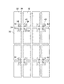
図2は、画素電極32を示す図である。有機エレクトロルミネッセンス表示装置は、相互に分離された複数の画素電極32を有する。絶縁層28を貫通するコンタクト34によって、それぞれの画素電極32は、いずれかの薄膜トランジスタ24に電気的に接続されている。隣同士の2つ以上の画素電極32にそれぞれが接続する2つ以上のコンタクト34は、隣り合うように配置されている。つまり、複数のコンタクト34が一か所に集まるようになっている。
FIG. 2 is a diagram showing the
それぞれの画素電極32の少なくとも中央部を囲むように、樹脂などの絶縁体からバンク36が設けられている。バンク36に囲まれた画素電極32上に、図1に示すように有機エレクトロルミネッセンス層38が形成されている。有機エレクトロルミネッセンス層38の一部はバンク36にも載るようになっている。バンク36は、図2に示すように、隣り合う2つ以上のコンタクト34を連続的に覆う被覆部40を有する。
A
有機エレクトロルミネッセンス層38は、少なくとも発光層を含み、さらに、電子輸送層、正孔輸送層、電子注入層及び正孔注入層のうち少なくとも一層を含む。有機エレクトロルミネッセンス層38を構成する少なくとも一層は有機材料からなる。有機エレクトロルミネッセンス層38は、蒸着又はスパッタリングによって形成する。有機エレクトロルミネッセンス層38は、異なる色を発する複数の発光層を重ねて、混色により白色光を発するように構成されている。
The
有機エレクトロルミネッセンス層38上からバンク36上に至るように光透過性の共通電極42が形成されている。共通電極42は、全ての画素電極32の全体を覆うように形成されている。画素電極32と共通電極42の間に有機エレクトロルミネッセンス層38が配置されている。画素電極32及び共通電極42に電圧をかけることにより各々から正孔と電子を有機エレクトロルミネッセンス層38に注入する。注入された正孔と電子が発光層で結合して光を発する。
A light-transmissive
有機エレクトロルミネッセンス表示装置は、ガラスなどからなる光透過性の第2基板44を有する。第2基板44は、第1基板10と間隔をあけて対向するように配置されている。第2基板44の第1基板10側の面には、カラーフィルタ層46が設けられている。カラーフィルタ層46が、有機エレクトロルミネッセンス層38に重なる。有機エレクトロルミネッセンス層38とカラーフィルタ層46との間には、スペース48が形成されている。つまり、中空封止が適用されている。変形例として樹脂をスペース48に充填してもよい。第2基板44の第1基板10側の面には、ブラックマトリクス層50が形成されている。
The organic electroluminescence display device has a light-transmissive
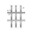
図3は、ブラックマトリクス層50を示す図である。ブラックマトリクス層50にスペーサ52が設けられている。ブラックマトリクス層50には、スペーサ52に載るように配線54が設けられている。配線54は、スペーサ52に載ることで、凸部56が形成されている。配線54は、第2基板44上のブラックマトリクス層50上に形成するので、フォトプロセスや焼成プロセスを適用することが可能であり、材料選択の幅が広い。
FIG. 3 is a diagram showing the
製造プロセスでは、第2基板44の一方の面にブラックマトリクス層50を形成し、同じ面にブラックマトリクス層50を形成し、同じ側でブラックマトリクス層50にスペーサ52を設け、配線54を形成するという順序で行う。
In the manufacturing process, the
ブラックマトリクス層50は、図1及び図2に示すようにバンク36に重なる。ブラックマトリクス層50は、スペーサ52を介してバンク36上に配置されている。スペーサ52があることでブラックマトリクス層50とバンク36のギャップが形成されるが、そのギャップの大きさは均一化される。また、スペーサ52があることで、有機エレクトロルミネッセンス層38とカラーフィルタ層46との間に異物があっても、ギャップが大きくなるので、有機エレクトロルミネッセンス層38を押しつぶさないようになる。
The
配線54の凸部56がバンク36の上方で共通電極42と電気的に接続する。凸部56があることで、配線54と共通電極42を安定的に接触させることができる。変形例として、図1に示すスペース48に樹脂を充填する場合、その樹脂が共通電極42の上面を覆ってしまうとしても、凸部56を樹脂に押し込んでこれを共通電極42に接触させる。バンク36の被覆部40は、2つ以上のコンタクト34を連続的に覆うことから広くなっているので、その上にスペーサ52が位置する。被覆部40上で配線54の凸部56が共通電極42と電気的に接続する。
The
本実施形態によれば、相互に電気的に接続する配線54及び共通電極42の全体の導電性は、共通電極42自体の導電性よりも高くなっている。また、配線54は、ブラックマトリクス層50に重なるように、かつ、はみ出さないように形成されるので、光の透過を妨げないようになっている。したがって、高い光透過性と高い導電性を両立させることができる。
According to the present embodiment, the overall conductivity of the
本発明は、上述した実施形態に限定されるものではなく種々の変形が可能である。例えば、実施形態で説明した構成は、実質的に同一の構成、同一の作用効果を奏する構成又は同一の目的を達成することができる構成で置き換えることができる。 The present invention is not limited to the above-described embodiments, and various modifications can be made. For example, the configuration described in the embodiment can be replaced with substantially the same configuration, a configuration that exhibits the same operational effects, or a configuration that can achieve the same purpose.
10 第1基板、12 半導体層、14 ゲート絶縁膜、16 ゲート電極、18 層間絶縁膜、20 ソース電極、22 ドレイン電極、24 薄膜トランジスタ、26 パッシベーション膜、28 絶縁層、30 光反射層、32 画素電極、34 コンタクト、36 バンク、38 有機エレクトロルミネッセンス層、40 被覆部、42 共通電極、44 第2基板、46 カラーフィルタ層、48 スペース、50 ブラックマトリクス層、52 スペーサ、54 配線、56 凸部。 10 First substrate, 12 Semiconductor layer, 14 Gate insulating film, 16 Gate electrode, 18 Interlayer insulating film, 20 Source electrode, 22 Drain electrode, 24 Thin film transistor, 26 Passivation film, 28 Insulating layer, 30 Light reflecting layer, 32 Pixel electrode , 34 contacts, 36 banks, 38 organic electroluminescence layers, 40 covering portions, 42 common electrodes, 44 second substrate, 46 color filter layers, 48 spaces, 50 black matrix layers, 52 spacers, 54 wirings, 56 convex portions.
Claims (6)
第2の画素電極を備える第2の画素と、
第3の画素電極を備える第3の画素と、
第4の画素電極を備える第4の画素と、
前記第1の画素電極と第1のコンタクトを介して接続する第1の薄膜トランジスタと、
前記第2の画素電極と第2のコンタクトを介して接続する第2の薄膜トランジスタと、
前記第3の画素電極と第3のコンタクトを介して接続する第3の薄膜トランジスタと、
前記第4の画素電極と第4のコンタクトを介して接続する第4の薄膜トランジスタと、
前記第1の画素電極、前記第2の画素電極、前記第3の画素電極、及び前記第4の画素電極の各々の少なくとも中央部を囲むように設けられたバンクと、
前記第1の画素電極、前記第2の画素電極、前記第3の画素電極、及び前記第4の画素電極上に設けられた有機エレクトロルミネッセンス層と、
前記有機エレクトロルミネッセンス層上から前記バンク上に至るように形成された光透過性の共通電極と、
前記バンクに重なるブラックマトリクス層と、
前記ブラックマトリクス層に設けられた複数のスペーサと、
前記複数のスペーサに載るように前記ブラックマトリクス層に設けられた配線と、
を有し、
前記第1の画素、前記第2の画素、前記第3の画素、及び前記第4の画素は、互いに隣接するように2行2列に配列し、
前記第1のコンタクト、前記第2のコンタクト、前記第3のコンタクト、及び前記第4のコンタクトは、互いに隣接し、
前記ブラックマトリクス層は、前記複数のスペーサを介して前記バンク上に配置され、
前記配線は、前記複数のスペーサに載ることで凸部が形成され、前記凸部が前記バンクの上方で前記共通電極と電気的に接続し、
前記ブラックマトリクス層は、第1の方向に延びる第1の部分と、前記第1の方向と交差する第2の方向に延びる第2の部分とを含むと共に、前記第1の部分と前記第2の部分とが交差する複数の交差部を備え、
前記複数の交差部は、平面的に見て、前記複数のスペーサの各々と重畳している第1の交差部と、前記複数のスペーサのいずれとも重畳していない第2の交差部と、を含み、
前記ブラックマトリクス層の前記第1の交差部は、平面的に見て、前記第1のコンタクト、前記第2のコンタクト、前記第3のコンタクト、及び前記第4のコンタクトと重畳し、
前記バンクは、前記第1のコンタクトと前記第2のコンタクトと前記第3のコンタクトと前記第4のコンタクトとを連続的に覆う被覆部を有し、
前記被覆部は、平面的に見て、前記複数のスペーサの一つ及び前記ブラックマトリクス層の前記第1の交差部と重畳することを特徴とする有機エレクトロルミネッセンス表示装置。 A first pixel comprising a first pixel electrode;
A second pixel comprising a second pixel electrode;
A third pixel comprising a third pixel electrode;
A fourth pixel comprising a fourth pixel electrode;
A first thin film transistor connected to the first pixel electrode via a first contact;
A second thin film transistor connected to the second pixel electrode via a second contact;
A third thin film transistor connected to the third pixel electrode via a third contact;
A fourth thin film transistor connected to the fourth pixel electrode via a fourth contact;
A bank provided to surround at least a central portion of each of the first pixel electrode, the second pixel electrode, the third pixel electrode, and the fourth pixel electrode ;
An organic electroluminescence layer provided on the first pixel electrode, the second pixel electrode, the third pixel electrode, and the fourth pixel electrode;
A light transmissive common electrode formed so as to extend from the organic electroluminescence layer to the bank;
A black matrix layer overlying the bank;
A plurality of spacers provided in the black matrix layer;
Wiring provided in the black matrix layer so as to be placed on the plurality of spacers;
Have
The first pixel, the second pixel, the third pixel, and the fourth pixel are arranged in 2 rows and 2 columns so as to be adjacent to each other,
The first contact, the second contact, the third contact, and the fourth contact are adjacent to each other;
The black matrix layer is disposed on the bank via the plurality of spacers,
The wiring is formed on the plurality of spacers to form a convex portion, and the convex portion is electrically connected to the common electrode above the bank,
The black matrix layer includes a first portion extending in a first direction and a second portion extending in a second direction intersecting the first direction, and the first portion and the second portion. It has a plurality of intersections that intersect
It said plurality of intersections, in plan view, the first cross section is overlapped with each of the plurality of spacers, and a second cross section which does not overlap with any of the plurality of spacers, only including,
The first intersection of the black matrix layer overlaps the first contact, the second contact, the third contact, and the fourth contact in plan view,
The bank has a covering portion that continuously covers the first contact, the second contact, the third contact, and the fourth contact;
The organic electroluminescence display device , wherein the covering portion overlaps with one of the plurality of spacers and the first intersecting portion of the black matrix layer in plan view.
前記第1の画素は、前記第1のコンタクトの側に位置する一つの第1の角部と、前記第1の角部とは異なる側に位置する三つの第2の角部と、を有し、
前記三つの第2の角部は、平面的に見て、前記ブラックマトリクス層の前記第2の交差部と隣接していることを特徴とする有機エレクトロルミネッセンス表示装置。 The organic electroluminescence display device according to claim 1,
The first pixel has one first corner located on the first contact side and three second corners located on a side different from the first corner. And
The three second corner portions are adjacent to the second intersecting portion of the black matrix layer as viewed in a plan view, the organic electroluminescence display device.
前記有機エレクトロルミネッセンス層は、白色光を発するように構成されていることを特徴とする有機エレクトロルミネッセンス表示装置。 In the organic electroluminescence display device according to claim 1 or 2,
The organic electroluminescence display device, wherein the organic electroluminescence layer is configured to emit white light.
前記有機エレクトロルミネッセンス層に重なるカラーフィルタ層をさらに有することを特徴とする有機エレクトロルミネッセンス表示装置。 The organic electroluminescence display device according to any one of claims 1 to 3,
The organic electroluminescence display device further comprising a color filter layer overlapping the organic electroluminescence layer.
前記有機エレクトロルミネッセンス層と前記カラーフィルタ層との間にスペースが形成されていることを特徴とする有機エレクトロルミネッセンス表示装置。 The organic electroluminescence display device according to claim 4,
A space is formed between the organic electroluminescence layer and the color filter layer. An organic electroluminescence display device, wherein:
前記バンクは、前記被覆部から第1の方向に延びる第1の領域と、前記被覆部から第2の方向に延びる第2の領域と、を有し、
前記被覆部の前記第1の方向の幅は、前記第2の領域の前記第1の方向の幅よりも大きく、
前記被覆部の前記第2の方向の幅は、前記第1の領域の前記第2の方向の幅よりも大きいことを特徴とする有機エレクトロルミネッセンス表示装置。 In the organic electroluminescence display device according to any one of claims 1 to 5,
The bank has a first region extending in a first direction from the covering portion, and a second region extending in a second direction from the covering portion,
The width of the covering portion in the first direction is larger than the width of the second region in the first direction,
The organic electroluminescence display device , wherein a width of the covering portion in the second direction is larger than a width of the first region in the second direction .
Priority Applications (5)
| Application Number | Priority Date | Filing Date | Title |
|---|---|---|---|
| JP2013060351A JP5991490B2 (en) | 2013-03-22 | 2013-03-22 | Organic electroluminescence display device |
| US14/207,765 US9231036B2 (en) | 2013-03-22 | 2014-03-13 | Organic electroluminescence display device |
| US14/800,031 US9397148B2 (en) | 2013-03-22 | 2015-07-15 | Organic electroluminescence display device |
| US15/171,754 US20160276420A1 (en) | 2013-03-22 | 2016-06-02 | Organic electroluminescence display device |
| US15/585,292 US10236336B2 (en) | 2013-03-22 | 2017-05-03 | Organic electroluminescence display device with spacers |
Applications Claiming Priority (1)
| Application Number | Priority Date | Filing Date | Title |
|---|---|---|---|
| JP2013060351A JP5991490B2 (en) | 2013-03-22 | 2013-03-22 | Organic electroluminescence display device |
Publications (3)
| Publication Number | Publication Date |
|---|---|
| JP2014186844A JP2014186844A (en) | 2014-10-02 |
| JP2014186844A5 JP2014186844A5 (en) | 2015-08-13 |
| JP5991490B2 true JP5991490B2 (en) | 2016-09-14 |
Family
ID=51568468
Family Applications (1)
| Application Number | Title | Priority Date | Filing Date |
|---|---|---|---|
| JP2013060351A Active JP5991490B2 (en) | 2013-03-22 | 2013-03-22 | Organic electroluminescence display device |
Country Status (2)
| Country | Link |
|---|---|
| US (4) | US9231036B2 (en) |
| JP (1) | JP5991490B2 (en) |
Families Citing this family (28)
| Publication number | Priority date | Publication date | Assignee | Title |
|---|---|---|---|---|
| CN103151369B (en) * | 2013-02-06 | 2016-01-06 | 京东方科技集团股份有限公司 | A kind of dot structure and preparation method thereof |
| CN104752476B (en) * | 2013-12-31 | 2018-05-22 | 乐金显示有限公司 | Organic light-emitting display device and its manufacturing method |
| KR102205401B1 (en) * | 2014-01-14 | 2021-01-21 | 삼성디스플레이 주식회사 | Organic luminescence emitting display device |
| DE102014100770A1 (en) * | 2014-01-23 | 2015-07-23 | Osram Opto Semiconductors Gmbh | Light-emitting device and method for producing a light-emitting device |
| JP6220300B2 (en) * | 2014-03-20 | 2017-10-25 | 株式会社ジャパンディスプレイ | Method for manufacturing organic electroluminescent display device and organic electroluminescent display device |
| US10719585B2 (en) * | 2014-07-08 | 2020-07-21 | Hewlett-Packard Development Company, L.P. | Composite document access |
| JP6487173B2 (en) | 2014-10-08 | 2019-03-20 | 株式会社ジャパンディスプレイ | Display device and manufacturing method thereof |
| KR20160071581A (en) * | 2014-12-11 | 2016-06-22 | 삼성디스플레이 주식회사 | Organic light emitting display apparatus and method for manufacturing the same |
| KR102429283B1 (en) * | 2015-05-27 | 2022-08-05 | 삼성전자주식회사 | Display device |
| CN112436045B (en) | 2015-05-27 | 2023-12-19 | 三星电子株式会社 | display device |
| JP2017003849A (en) * | 2015-06-12 | 2017-01-05 | 株式会社ジャパンディスプレイ | Display device |
| US10196919B2 (en) | 2015-06-29 | 2019-02-05 | Rolls-Royce North American Technologies Inc. | Turbine shroud segment with load distribution springs |
| US10094234B2 (en) | 2015-06-29 | 2018-10-09 | Rolls-Royce North America Technologies Inc. | Turbine shroud segment with buffer air seal system |
| JP6685675B2 (en) | 2015-09-07 | 2020-04-22 | 株式会社Joled | Organic EL device, organic EL display panel using the same, and method for manufacturing organic EL display panel |
| KR20170040425A (en) * | 2015-10-02 | 2017-04-13 | 삼성디스플레이 주식회사 | Organic light emitting diode display and method for manufacturing the same |
| KR102508727B1 (en) * | 2015-11-19 | 2023-03-14 | 삼성디스플레이 주식회사 | Display device |
| KR101765102B1 (en) * | 2015-11-30 | 2017-08-04 | 엘지디스플레이 주식회사 | Organic light emitting display device and method of manufacturing the same |
| KR102416470B1 (en) * | 2015-12-21 | 2022-07-04 | 엘지디스플레이 주식회사 | Display panel with luminance efficiency improvement, display device comprising thereof, and method of fabricating the display panel |
| US10020351B2 (en) * | 2016-06-24 | 2018-07-10 | Lg Display Co., Ltd. | Electroluminescence display device |
| KR20180068552A (en) * | 2016-12-14 | 2018-06-22 | 엘지디스플레이 주식회사 | Organic light emitting display device and method for fabricating the same |
| KR102662681B1 (en) | 2016-12-26 | 2024-04-30 | 엘지디스플레이 주식회사 | Display device with integrated touch screen and method for fabricating the same |
| CN107634012B (en) * | 2017-09-13 | 2021-05-07 | 京东方科技集团股份有限公司 | Packaging substrate, preparation method thereof, display panel and display device |
| CN107706218A (en) * | 2017-09-25 | 2018-02-16 | 深圳市华星光电半导体显示技术有限公司 | Organic electroluminescence display device and method of manufacturing same |
| CN107681063A (en) * | 2017-10-11 | 2018-02-09 | 京东方科技集团股份有限公司 | Array base palte and preparation method thereof, display device |
| CN109671738B (en) * | 2017-10-13 | 2021-02-05 | 京东方科技集团股份有限公司 | Array substrate, display panel, manufacturing method of display panel and display device |
| CN108022961A (en) * | 2017-11-09 | 2018-05-11 | 上海天马有机发光显示技术有限公司 | Organic electroluminescence display panel and display device |
| CN109638177B (en) * | 2019-01-18 | 2022-01-11 | 京东方科技集团股份有限公司 | Display substrate, preparation method thereof and display panel |
| CN110112194A (en) * | 2019-04-30 | 2019-08-09 | 深圳市华星光电半导体显示技术有限公司 | Organic light emitting display panel and preparation method thereof |
Family Cites Families (30)
| Publication number | Priority date | Publication date | Assignee | Title |
|---|---|---|---|---|
| CN100341042C (en) * | 1997-02-17 | 2007-10-03 | 精工爱普生株式会社 | Display device |
| US6277679B1 (en) * | 1998-11-25 | 2001-08-21 | Semiconductor Energy Laboratory Co., Ltd. | Method of manufacturing thin film transistor |
| US6559594B2 (en) * | 2000-02-03 | 2003-05-06 | Semiconductor Energy Laboratory Co., Ltd. | Light-emitting device |
| JP4713010B2 (en) | 2000-05-08 | 2011-06-29 | 株式会社半導体エネルギー研究所 | Light emitting device and manufacturing method thereof |
| US6608449B2 (en) | 2000-05-08 | 2003-08-19 | Semiconductor Energy Laboratory Co., Ltd. | Luminescent apparatus and method of manufacturing the same |
| US6630785B1 (en) * | 2000-05-30 | 2003-10-07 | Ritdisplay Corporation | Surface treatment process for fabricating a panel of an organic light emitting device |
| JP2003092192A (en) * | 2001-09-18 | 2003-03-28 | Matsushita Electric Ind Co Ltd | Organic electroluminescent display device and method for manufacturing the same |
| US6815723B2 (en) * | 2001-12-28 | 2004-11-09 | Semiconductor Energy Laboratory Co., Ltd. | Light emitting device, method of manufacturing the same, and manufacturing apparatus therefor |
| US7897979B2 (en) * | 2002-06-07 | 2011-03-01 | Semiconductor Energy Laboratory Co., Ltd. | Light emitting device and manufacturing method thereof |
| JP4216008B2 (en) * | 2002-06-27 | 2009-01-28 | 株式会社半導体エネルギー研究所 | LIGHT EMITTING DEVICE AND ITS MANUFACTURING METHOD, AND VIDEO CAMERA, DIGITAL CAMERA, GOGGLE TYPE DISPLAY, CAR NAVIGATION, PERSONAL COMPUTER, DVD PLAYER, ELECTRONIC GAME EQUIPMENT, OR PORTABLE INFORMATION TERMINAL HAVING THE LIGHT EMITTING DEVICE |
| JP4062171B2 (en) * | 2003-05-28 | 2008-03-19 | ソニー株式会社 | Manufacturing method of laminated structure |
| JP4489472B2 (en) * | 2004-03-19 | 2010-06-23 | 株式会社 日立ディスプレイズ | Organic electroluminescence display device |
| JP2006278241A (en) | 2005-03-30 | 2006-10-12 | Tohoku Pioneer Corp | Spontaneous light emitting panel and manufacturing method of the same |
| JP4702136B2 (en) | 2006-03-28 | 2011-06-15 | セイコーエプソン株式会社 | LIGHT EMITTING DEVICE AND ELECTRONIC DEVICE |
| JP2007287354A (en) * | 2006-04-12 | 2007-11-01 | Hitachi Displays Ltd | Organic el display device |
| JP2009128671A (en) | 2007-11-26 | 2009-06-11 | Canon Inc | Organic el display element and its manufacturing method |
| TWI406031B (en) * | 2008-07-08 | 2013-08-21 | Casio Computer Co Ltd | Display apparatus |
| US7999454B2 (en) * | 2008-08-14 | 2011-08-16 | Global Oled Technology Llc | OLED device with embedded chip driving |
| JP2012042490A (en) * | 2008-12-16 | 2012-03-01 | Sharp Corp | Liquid crystal display panel and liquid crystal display device |
| KR101795691B1 (en) * | 2010-11-11 | 2017-11-09 | 삼성디스플레이 주식회사 | Display apparatus |
| KR101845332B1 (en) * | 2011-06-13 | 2018-05-21 | 삼성디스플레이 주식회사 | Organic light emitting display device and method for manufacturing the same |
| US9647229B2 (en) | 2011-10-26 | 2017-05-09 | Dai Nippon Printing Co., Ltd. | Color filter for organic electroluminescence display device, and organic electroluminescence display device |
| TWI577006B (en) * | 2011-11-29 | 2017-04-01 | 半導體能源研究所股份有限公司 | Sealed structure, light-emitting device, electronic device, and lighting device |
| US9153628B2 (en) * | 2012-02-08 | 2015-10-06 | Joled Inc. | Display panel having an inter-layer insulation layer with planar and protruding regions |
| KR102105287B1 (en) * | 2012-08-01 | 2020-04-28 | 가부시키가이샤 한도오따이 에네루기 켄큐쇼 | Display device |
| US20150212540A1 (en) * | 2012-08-10 | 2015-07-30 | Sharp Kabushiki Kaisha | Light diffusing touch panel and manufacturing method for same, as well as display device |
| KR101927334B1 (en) * | 2012-09-10 | 2018-12-10 | 엘지디스플레이 주식회사 | Organic electro luminescence device and method for fabricating the same |
| JP6077279B2 (en) * | 2012-11-20 | 2017-02-08 | 株式会社ジャパンディスプレイ | Display device |
| KR102022394B1 (en) * | 2013-02-12 | 2019-09-19 | 삼성디스플레이 주식회사 | Organic light emitting display device |
| TWI538191B (en) * | 2013-03-04 | 2016-06-11 | 群創光電股份有限公司 | Color oled display |
-
2013
- 2013-03-22 JP JP2013060351A patent/JP5991490B2/en active Active
-
2014
- 2014-03-13 US US14/207,765 patent/US9231036B2/en active Active
-
2015
- 2015-07-15 US US14/800,031 patent/US9397148B2/en active Active
-
2016
- 2016-06-02 US US15/171,754 patent/US20160276420A1/en not_active Abandoned
-
2017
- 2017-05-03 US US15/585,292 patent/US10236336B2/en active Active
Also Published As
| Publication number | Publication date |
|---|---|
| US20160276420A1 (en) | 2016-09-22 |
| US20140284572A1 (en) | 2014-09-25 |
| US9231036B2 (en) | 2016-01-05 |
| US20170236893A1 (en) | 2017-08-17 |
| US10236336B2 (en) | 2019-03-19 |
| US9397148B2 (en) | 2016-07-19 |
| JP2014186844A (en) | 2014-10-02 |
| US20150325629A1 (en) | 2015-11-12 |
Similar Documents
| Publication | Publication Date | Title |
|---|---|---|
| JP5991490B2 (en) | Organic electroluminescence display device | |
| CN107565048B (en) | Preparation method of array substrate, array substrate and display device | |
| US20180342563A1 (en) | Oled display substrate and manufacturing method thereof, display panel and display apparatus | |
| KR102242241B1 (en) | Display device with built-in touch sensor | |
| US8890151B2 (en) | Organic light-emitting display apparatus | |
| CN108110037B (en) | Flexible display screen | |
| US11164918B2 (en) | Organic light emitting diode display panel having connection portion connecting organic light emitting diode to peripheral circuit and manufacturing method thereof | |
| JP2014186844A5 (en) | ||
| US10490603B2 (en) | Display device | |
| JP2015108751A (en) | Organic electroluminescence display device | |
| CN109599426B (en) | Display panel and display device | |
| CN103839965A (en) | Organic light emitting diode display device and method of fabricating the same | |
| JP2014192149A (en) | Oled display panel and manufacturing method thereof | |
| JP2017010854A (en) | Display device | |
| US20180294322A1 (en) | Organic Light Emitting Display Panel | |
| JP2017168397A (en) | Display device | |
| JP5500978B2 (en) | Organic EL device | |
| JP2022108901A (en) | Display device | |
| KR20160069289A (en) | Organic light emitting display apparatus and thin film deposition mask for manufacturing the same | |
| JP2014191329A (en) | Double-sided display apparatus | |
| JP2006011059A (en) | Optoelectronic device and electronic apparatus | |
| KR20160047052A (en) | High Luminance Large Area Organic Light Emitting Diode Display | |
| JP2017220174A (en) | Display device | |
| JP2015176766A (en) | Display device and method of manufacturing display device | |
| JP6230627B2 (en) | Light emitting device |
Legal Events
| Date | Code | Title | Description |
|---|---|---|---|
| A521 | Request for written amendment filed |
Free format text: JAPANESE INTERMEDIATE CODE: A523 Effective date: 20150630 |
|
| A621 | Written request for application examination |
Free format text: JAPANESE INTERMEDIATE CODE: A621 Effective date: 20150630 |
|
| A977 | Report on retrieval |
Free format text: JAPANESE INTERMEDIATE CODE: A971007 Effective date: 20160519 |
|
| A131 | Notification of reasons for refusal |
Free format text: JAPANESE INTERMEDIATE CODE: A131 Effective date: 20160531 |
|
| A521 | Request for written amendment filed |
Free format text: JAPANESE INTERMEDIATE CODE: A523 Effective date: 20160627 |
|
| TRDD | Decision of grant or rejection written | ||
| A01 | Written decision to grant a patent or to grant a registration (utility model) |
Free format text: JAPANESE INTERMEDIATE CODE: A01 Effective date: 20160726 |
|
| A61 | First payment of annual fees (during grant procedure) |
Free format text: JAPANESE INTERMEDIATE CODE: A61 Effective date: 20160802 |
|
| R150 | Certificate of patent or registration of utility model |
Ref document number: 5991490 Country of ref document: JP Free format text: JAPANESE INTERMEDIATE CODE: R150 |
|
| R250 | Receipt of annual fees |
Free format text: JAPANESE INTERMEDIATE CODE: R250 |
|
| R250 | Receipt of annual fees |
Free format text: JAPANESE INTERMEDIATE CODE: R250 |
|
| R250 | Receipt of annual fees |
Free format text: JAPANESE INTERMEDIATE CODE: R250 |
|
| R250 | Receipt of annual fees |
Free format text: JAPANESE INTERMEDIATE CODE: R250 |
|
| R250 | Receipt of annual fees |
Free format text: JAPANESE INTERMEDIATE CODE: R250 |