JP2012129453A - Semiconductor device and method of manufacturing semiconductor device - Google Patents
Semiconductor device and method of manufacturing semiconductor device Download PDFInfo
- Publication number
- JP2012129453A JP2012129453A JP2010281649A JP2010281649A JP2012129453A JP 2012129453 A JP2012129453 A JP 2012129453A JP 2010281649 A JP2010281649 A JP 2010281649A JP 2010281649 A JP2010281649 A JP 2010281649A JP 2012129453 A JP2012129453 A JP 2012129453A
- Authority
- JP
- Japan
- Prior art keywords
- element isolation
- oxide film
- isolation trench
- opening width
- semiconductor substrate
- Prior art date
- Legal status (The legal status is an assumption and is not a legal conclusion. Google has not performed a legal analysis and makes no representation as to the accuracy of the status listed.)
- Pending
Links
Images


Classifications
-
- H—ELECTRICITY
- H01—ELECTRIC ELEMENTS
- H01L—SEMICONDUCTOR DEVICES NOT COVERED BY CLASS H10
- H01L21/00—Processes or apparatus adapted for the manufacture or treatment of semiconductor or solid state devices or of parts thereof
- H01L21/70—Manufacture or treatment of devices consisting of a plurality of solid state components formed in or on a common substrate or of parts thereof; Manufacture of integrated circuit devices or of parts thereof
- H01L21/71—Manufacture of specific parts of devices defined in group H01L21/70
- H01L21/76—Making of isolation regions between components
- H01L21/762—Dielectric regions, e.g. EPIC dielectric isolation, LOCOS; Trench refilling techniques, SOI technology, use of channel stoppers
- H01L21/76224—Dielectric regions, e.g. EPIC dielectric isolation, LOCOS; Trench refilling techniques, SOI technology, use of channel stoppers using trench refilling with dielectric materials
- H01L21/76232—Dielectric regions, e.g. EPIC dielectric isolation, LOCOS; Trench refilling techniques, SOI technology, use of channel stoppers using trench refilling with dielectric materials of trenches having a shape other than rectangular or V-shape, e.g. rounded corners, oblique or rounded trench walls
-
- H—ELECTRICITY
- H10—SEMICONDUCTOR DEVICES; ELECTRIC SOLID-STATE DEVICES NOT OTHERWISE PROVIDED FOR
- H10B—ELECTRONIC MEMORY DEVICES
- H10B41/00—Electrically erasable-and-programmable ROM [EEPROM] devices comprising floating gates
- H10B41/40—Electrically erasable-and-programmable ROM [EEPROM] devices comprising floating gates characterised by the peripheral circuit region
- H10B41/42—Simultaneous manufacture of periphery and memory cells
Landscapes
- Engineering & Computer Science (AREA)
- Manufacturing & Machinery (AREA)
- Physics & Mathematics (AREA)
- Condensed Matter Physics & Semiconductors (AREA)
- General Physics & Mathematics (AREA)
- Computer Hardware Design (AREA)
- Microelectronics & Electronic Packaging (AREA)
- Power Engineering (AREA)
- Semiconductor Memories (AREA)
- Non-Volatile Memory (AREA)
- Element Separation (AREA)
Abstract
Description
本発明の実施形態は、素子分離溝を塗布系の材料で埋め込む素子分離構造を備えた半導体装置および半導体装置の製造方法に関する。 Embodiments described herein relate generally to a semiconductor device including an element isolation structure in which an element isolation groove is embedded with a coating material, and a method for manufacturing the semiconductor device.
フラッシュメモリ装置等の半導体装置においては、平坦性および微細化に優れるSTI(Shallow Trench Isolation)による素子分離構造が使用されている。このSTI構造は、半導体基板の表面に素子分離溝を形成し、この素子分離溝内に素子分離絶縁膜を埋め込んで構成される。STI構造の埋め込み材料としては、微細化が進むにつれて、埋め込み性が良い塗布系の材料が使用されている。 In a semiconductor device such as a flash memory device, an element isolation structure by STI (Shallow Trench Isolation) excellent in flatness and miniaturization is used. This STI structure is configured by forming an element isolation trench on the surface of a semiconductor substrate and embedding an element isolation insulating film in the element isolation trench. As the filling material of the STI structure, as the miniaturization progresses, a coating material having good filling properties is used.
上記塗布系の材料は、塗布後に熱処理を行って塗布膜を酸化膜に置換する熱工程が必要であり、この熱処理時に塗布膜の体積収縮量が大きいという特性がある。このため、フラッシュメモリ装置の周辺回路領域における幅広の素子分離溝を有するSTI構造においては、上記塗布膜の大きな体積収縮によって素子分離溝に大きな応力が作用し、結晶欠陥が発生することがあった。尚、上記塗布膜に代えてCVD(chemical vapor deposition)膜で素子分離溝を埋め込む構成も、従来より使用されているが、微細化が進むと、メモリセル領域においてライン曲がり(Line Bending)が発生することがあるため、埋め込み材料として塗布膜の使用が要望されている。 The material of the coating system has a characteristic that a heat process is performed after coating to replace the coating film with an oxide film, and the volume shrinkage of the coating film is large during the heat treatment. For this reason, in the STI structure having a wide element isolation groove in the peripheral circuit region of the flash memory device, a large stress may act on the element isolation groove due to the large volume shrinkage of the coating film, and crystal defects may occur. . In addition, a structure in which an element isolation groove is embedded with a CVD (chemical vapor deposition) film instead of the above-described coating film is also used conventionally. However, as the miniaturization progresses, line bending occurs in the memory cell region. Therefore, use of a coating film as a filling material is desired.
そこで、素子分離溝を塗布系の材料で埋め込む素子分離構造において、熱処理時に素子分離溝に大きな応力が作用することを防止できる半導体装置および半導体装置の製造方法を提供する。 Accordingly, there are provided a semiconductor device and a method for manufacturing the semiconductor device that can prevent a large stress from acting on the element isolation groove during heat treatment in the element isolation structure in which the element isolation groove is embedded with a coating material.
本実施形態の半導体装置は、半導体基板と、前記半導体基板上に設けられ複数のメモリセルが形成されたメモリセル領域と、前記半導体基板上に設けられた周辺回路領域と、前記メモリセル領域に形成され、第1の開口幅を有する第1の素子分離溝と、前記周辺回路領域に形成され、第1の開口幅より大きい第2の開口幅を有する第2の素子分離溝とを備える。そして、前記第1の素子分離溝の内面に形成された第1の酸化膜と、前記第1の酸化膜上に形成されて前記第1の素子分離溝内に埋め込まれた第1の塗布型酸化膜とを備える。更に、前記第2の素子分離溝の内面のうちの側部に形成された第2の酸化膜と、前記第2の素子分離溝の内面のうちの底部上に形成された第3の酸化膜と、前記第3の酸化膜上に形成されて前記第2の素子分離溝内に埋め込まれた第2の塗布型酸化膜とを備える。 The semiconductor device according to the present embodiment includes a semiconductor substrate, a memory cell region provided on the semiconductor substrate and formed with a plurality of memory cells, a peripheral circuit region provided on the semiconductor substrate, and the memory cell region. A first element isolation groove formed and having a first opening width; and a second element isolation groove formed in the peripheral circuit region and having a second opening width larger than the first opening width. A first oxide film formed on the inner surface of the first element isolation trench; and a first coating type formed on the first oxide film and embedded in the first element isolation trench. And an oxide film. Further, a second oxide film formed on a side portion of the inner surface of the second element isolation groove, and a third oxide film formed on a bottom portion of the inner surface of the second element isolation groove. And a second coating type oxide film formed on the third oxide film and embedded in the second element isolation trench.
本実施形態の半導体装置の製造方法は、半導体基板上にゲート絶縁膜を形成する工程と、前記ゲート絶縁膜上に浮遊ゲート電極用の導電層を形成する工程と、前記導電層、前記ゲート絶縁膜および前記半導体基板を加工して、メモリセル領域に第1の開口幅を有する第1の素子分離溝を形成し、周辺回路領域に第1の開口幅より大きい第2の開口幅を有する第2の素子分離溝を形成する工程とを備える。そして、前記第1の素子分離溝の内面、前記第2の素子分離溝の内面、前記ゲート絶縁膜の側部、前記導体層の側部および前記導体層の上面に酸化膜を形成する工程と、前記酸化膜上にレジストを形成する工程と、前記レジストにおける前記周辺回路領域を開口する工程と、前記周辺回路領域の前記第2の素子分離溝の底部の前記酸化膜を加工して前記底部の半導体基板を露出させる工程とを備える。更に、前記レジストを剥離する工程と、前記第2の素子分離溝の底部の半導体基板が露出している部分上にCVD法により選択的にCVD酸化膜を形成する工程と、前記酸化膜および前記CVD酸化膜の上に塗布型酸化膜を形成し、前記第1の素子分離溝および前記第2の素子分離溝を埋め込む工程とを備える。 The manufacturing method of the semiconductor device of this embodiment includes a step of forming a gate insulating film on a semiconductor substrate, a step of forming a conductive layer for a floating gate electrode on the gate insulating film, the conductive layer, and the gate insulation. The film and the semiconductor substrate are processed to form a first element isolation groove having a first opening width in the memory cell region, and a second opening width having a second opening width larger than the first opening width in the peripheral circuit region. Forming a second element isolation trench. Forming an oxide film on the inner surface of the first element isolation groove, the inner surface of the second element isolation groove, the side portion of the gate insulating film, the side portion of the conductor layer, and the upper surface of the conductor layer; Forming a resist on the oxide film; opening the peripheral circuit region in the resist; and processing the oxide film at the bottom of the second element isolation trench in the peripheral circuit region to form the bottom Exposing the semiconductor substrate. A step of removing the resist; a step of selectively forming a CVD oxide film by a CVD method on a portion where the semiconductor substrate at the bottom of the second element isolation trench is exposed; and the oxide film and the Forming a coating type oxide film on the CVD oxide film, and embedding the first element isolation groove and the second element isolation groove.
以下、複数の実施形態について、図面を参照して説明する。尚、各実施形態において、実質的に同一の構成部位には同一の符号を付し、説明を省略する。但し、図面は模式的なものであり、厚みと平面寸法との関係、各層の厚みの比率等は現実のものとは異なる。 Hereinafter, a plurality of embodiments will be described with reference to the drawings. In each embodiment, substantially the same components are assigned the same reference numerals, and description thereof is omitted. However, the drawings are schematic, and the relationship between the thickness and the planar dimensions, the ratio of the thickness of each layer, and the like are different from the actual ones.
(第1実施形態)
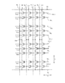
まず、図1は、第1実施形態のNAND型のフラッシュメモリ装置のメモリセル領域に形成されるメモリセルアレイの一部を示す等価回路図である。この図1に示すように、NAND型フラッシュメモリ装置のメモリセルアレイは、2個の選択ゲートトランジスタTrs1、Trs2と、当該選択ゲートトランジスタTrs1、Trs2間に対して直列接続された複数個(例えば32個)のメモリセルトランジスタTrmとからなるNANDセルユニットSUが行列状に形成されることにより構成されている。NANDセルユニットSU内において、複数個のメモリセルトランジスタTrmは隣接するもの同士でソース/ドレイン領域を共用して形成されている。
(First embodiment)
First, FIG. 1 is an equivalent circuit diagram showing a part of a memory cell array formed in the memory cell region of the NAND type flash memory device of the first embodiment. As shown in FIG. 1, the memory cell array of the NAND flash memory device includes two select gate transistors Trs1 and Trs2, and a plurality of (for example, 32) connected in series between the select gate transistors Trs1 and Trs2. ) Memory cell transistors Trm are formed in a matrix. In the NAND cell unit SU, a plurality of memory cell transistors Trm are formed by sharing adjacent source / drain regions.
図1中X方向(ワード線方向、ゲート幅方向に相当)に配列されたメモリセルトランジスタTrmは、ワード線WLにより共通接続されている。また、図1中X方向に配列された選択ゲートトランジスタTrs1は選択ゲート線SGL1で共通接続され、選択ゲートトランジスタTrs2は選択ゲート線SGL2で共通接続されている。選択ゲートトランジスタTrs1のドレイン領域にはビット線コンタクトCBが接続されている。このビット線コンタクトCBは、図1中X方向に直交するY方向(ゲート長方向、ビット線方向に相当)に延びるビット線BLに接続されている。また、選択ゲートトランジスタTrs2はソース領域を介して図1中X方向に延びるソース線SLに接続されている。 The memory cell transistors Trm arranged in the X direction (corresponding to the word line direction and the gate width direction) in FIG. 1 are commonly connected by a word line WL. Further, the selection gate transistors Trs1 arranged in the X direction in FIG. 1 are commonly connected by a selection gate line SGL1, and the selection gate transistors Trs2 are commonly connected by a selection gate line SGL2. A bit line contact CB is connected to the drain region of the select gate transistor Trs1. The bit line contact CB is connected to a bit line BL extending in the Y direction (corresponding to the gate length direction and the bit line direction) orthogonal to the X direction in FIG. The select gate transistor Trs2 is connected to a source line SL extending in the X direction in FIG. 1 through a source region.
図2(a)はメモリセル領域の一部のレイアウトパターンを示す平面図である。半導体基板としてのシリコン基板1に、図2(a)中Y方向に沿って延びる素子分離領域としてのSTI2が図2(a)中X方向に所定間隔で複数本形成されている。これによって、図2(a)中Y方向に沿って延びる活性領域3が図2(a)中X方向に分離形成されている。メモリセルトランジスタTrmのワード線WLは、活性領域3と直交する方向(図2(a)中X方向)に沿って延びるように形成されると共に、図2(a)中Y方向に所定間隔で複数本形成されている。
FIG. 2A is a plan view showing a layout pattern of a part of the memory cell region. A plurality of
また、一対の選択ゲートトランジスタの選択ゲート線SGL1が図2(a)中X方向に沿って延びるように形成されている。一対の選択ゲート線SGL1間の活性領域3にはビット線コンタクトCBがそれぞれ形成されている。ワード線WLと交差する活性領域3上にはメモリセルトランジスタのゲート電極MGが、選択ゲート線SGL1と交差する活性領域3上には選択ゲートトランジスタのゲート電極SGが形成されている。
Further, the selection gate line SGL1 of the pair of selection gate transistors is formed so as to extend along the X direction in FIG. Bit line contacts CB are formed in the
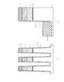
また、周辺回路領域を示す図2(b)において、メモリセル領域と同様にしてシリコン基板1に素子分離領域としてのSTI22が形成されており、このSTI22によって素子形成領域としての活性領域23が分離形成されている。上記活性領域23と直交する方向にゲート電極PG(周辺ゲート電極)が形成されている。周辺回路領域のSTI22の素子分離溝は、メモリセル領域のSTI2の素子分離溝の開口幅(第1の開口幅)よりも大きい開口幅(第2の開口幅)を有する。尚、開口幅とは、素子分離溝の短辺方向の幅を意味する。ゲート電極PGと活性領域23とが交差する部分に周辺回路用のトランジスタが形成されている。このようなトランジスタは、周辺回路領域の他の部分にも形成されていて、高耐圧トランジスタや低耐圧トランジスタなど、メモリセル領域のトランジスタを駆動するための種々のトランジスタとして形成されている。
In FIG. 2B showing the peripheral circuit region, an
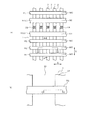
次に、本実施形態のメモリセル領域におけるゲート電極構造について図3を参照して、また、周辺回路領域におけるゲート電極構造について図4を参照して説明する。図3(a)は、図2(a)のA−A線(ビット線方向、Y方向)に沿う断面を模式的に示す図であり、図3(b)は、図2(a)のB−B線(ワード線方向、X方向)に沿う断面を模式的に示す図である。図4は、図2(b)のC−C線(ワード線方向、X方向)に沿う断面を模式的に示す図である。 Next, the gate electrode structure in the memory cell region of this embodiment will be described with reference to FIG. 3, and the gate electrode structure in the peripheral circuit region will be described with reference to FIG. 3A is a diagram schematically showing a cross section taken along the line AA (bit line direction, Y direction) of FIG. 2A, and FIG. 3B is a diagram of FIG. It is a figure which shows typically the cross section which follows a BB line (word line direction, X direction). FIG. 4 is a diagram schematically showing a cross section taken along line CC (word line direction, X direction) of FIG.
まず、メモリセル領域のゲート電極構造を示す図3(a)および(b)において、シリコン基板1の上部には、第1の開口幅を有する素子分離溝(第1の素子分離溝)4がX方向に離間して複数形成されている。これら素子分離溝4は、活性領域3を図2(a)中のX方向に分離している。素子分離溝4内には、素子分離絶縁膜5が形成されており、素子分離領域(STI)2を構成している。素子分離絶縁膜5は、素子分離溝4の内面に形成されたライナー酸化膜(第1の酸化膜)5aと、ライナー酸化膜5a上に形成された塗布型酸化膜(第1の塗布型酸化膜)5bとから構成される。
First, in FIGS. 3A and 3B showing the gate electrode structure in the memory cell region, an element isolation groove (first element isolation groove) 4 having a first opening width is formed on the
メモリセルトランジスタは、シリコン基板1に形成されたn型の拡散層6と、シリコン基板1上に形成されたゲート絶縁膜7と、ゲート絶縁膜7上に設けられたゲート電極MGとを含んで構成される。ゲート電極MGは、電荷蓄積層となる浮遊ゲート電極FGと、浮遊ゲート電極FG上に形成された電極間絶縁膜9と、電極間絶縁膜9上に形成された制御ゲート電極CGとを有する。拡散層6は、シリコン基板1の表層におけるメモリセルトランジスタのゲート電極MGの両脇に位置して形成されており、メモリセルトランジスタのソース/ドレイン領域を構成している。
The memory cell transistor includes an n-
ゲート絶縁膜7は、シリコン基板1(活性領域3)上に形成されている。ゲート絶縁膜7としては、例えばシリコン酸化膜を用いている。浮遊ゲート電極FGとしては、例えばリン等の不純物がドープされた多結晶シリコン層(導電層)8を用いている。電極間絶縁膜9は、素子分離絶縁膜5の上面、浮遊ゲート電極FGの上部側面、および、浮遊ゲート電極FGの上面に沿って形成されており、インターポリ絶縁膜、導電層間絶縁膜、電極間の絶縁膜として機能する。電極間絶縁膜9としては、例えばシリコン酸化膜/シリコン窒化膜/シリコン酸化膜の積層構造(それぞれの膜厚が、例えばいずれも3nmから10nmである)の膜、即ち、いわゆるONO膜を用いている。
The
制御ゲート電極CGは、メモリセルトランジスタのワード線WLとして機能する導電層10で構成される。導電層10は、例えばリン等の不純物がドープされた多結晶シリコン層10aと、この多結晶シリコン層10aの直上に形成されたタングステン(W)、コバルト(Co)、ニッケル(Ni)などの何れかの金属によってシリサイド化されたシリサイド層10bとの積層構造を有する。シリサイド層10bは、本実施形態の場合、例えばニッケルシリサイド(NiSi)で構成される。尚、導電層10をすべてシリサイド層10b(即ち、シリサイド層単体)で構成しても良い。
The control gate electrode CG is composed of the
また、図3(a)に示すように、メモリセルトランジスタのゲート電極MGは、Y方向に並設されており、各ゲート電極MGは電極分離用の溝17によって互いに電気的に分離されている。この溝17内にはメモリセル間絶縁膜11が形成されている。このメモリセル間絶縁膜11としては、例えばTEOS(tetraethyl orthosilicate)を用いたシリコン酸化膜または低誘電率絶縁膜を用いている。メモリセル間絶縁膜11の上面、制御ゲート電極CGの側面および上面上には、例えばシリコン酸化膜からなる層間絶縁膜12が形成されている。
As shown in FIG. 3A, the gate electrodes MG of the memory cell transistors are juxtaposed in the Y direction, and the gate electrodes MG are electrically separated from each other by the
次に、周辺回路領域のゲート電極構造を示す図4において、シリコン基板1の上部には、所定間隔でSTI(素子分離領域)22が形成されており、このSTI22により活性領域(素子形成領域)23が分離されている。STI22は、メモリセル領域のSTI2の素子分離溝4の第1の開口幅よりも大きい第2の開口幅を有する素子分離溝(第2の素子分離溝)24と、この素子分離溝24内に形成された素子分離絶縁膜25とから構成される。素子分離絶縁膜25は、素子分離溝24の内面の側部に形成されたライナー酸化膜(第2の酸化膜)25aと、素子分離溝24の内面の底部に形成された底部酸化膜25c(第3の酸化膜)と、ライナー酸化膜25aおよび底部酸化膜25c上に形成された塗布型酸化膜(第2の塗布型酸化膜)25bとから構成される。
Next, in FIG. 4 showing the gate electrode structure in the peripheral circuit region, STI (element isolation region) 22 is formed at a predetermined interval on the
活性領域23の上には、メモリセルトランジスタのゲート絶縁膜7よりも膜厚が厚い高耐圧トランジスタ用のゲート絶縁膜26が形成されている。ゲート絶縁膜26としては、例えばシリコン酸化膜を用いている。ゲート絶縁膜26の上には、メモリセルトランジスタと同様にして、ゲート電極PGを構成する浮遊ゲート電極FG(多結晶シリコン層8)と、電極間絶縁膜9と、制御ゲート電極CG(導電層10)とが積層され、更に、制御ゲート電極CG上に層間絶縁膜12が形成されている。
On the
次に、本実施形態によるNAND型フラッシュメモリ装置の製造方法の一例を、図5〜図13に示す工程断面図を参照して説明する。尚、図5(a)〜図13(a)は、図3(b)に対応するメモリセル領域の断面構造の製造段階を模式的に示す。図5(b)〜図13(b)は、図4に対応する周辺回路領域の断面構造の製造段階を模式的に示す。 Next, an example of a method for manufacturing the NAND flash memory device according to the present embodiment will be described with reference to process cross-sectional views shown in FIGS. FIG. 5A to FIG. 13A schematically show the manufacturing stage of the cross-sectional structure of the memory cell region corresponding to FIG. FIG. 5B to FIG. 13B schematically show the manufacturing stage of the cross-sectional structure of the peripheral circuit region corresponding to FIG.
まず、図5に示すように、シリコン基板1の表面に、ゲート絶縁膜7として例えばシリコン酸化膜を例えば熱酸化法を用いて形成する。このゲート絶縁膜7は、メモリセルトランジスタのゲート絶縁膜として機能するものである。また、周辺回路領域において、高耐圧トランジスタを形成する部分には、メモリセルトランジスタのゲート絶縁膜7よりも膜厚が厚いゲート絶縁膜26として例えばシリコン酸化膜を周知の方法で形成する。
First, as shown in FIG. 5, for example, a silicon oxide film is formed as a
この後、浮遊ゲート電極FGとなる例えばドープト多結晶シリコン層8を例えば減圧CVD法により形成する。ドープト多結晶シリコン層8の不純物としては、例えばリン(P)を用いる。
Thereafter, for example, a doped
次に、図6に示すように、ドープト多結晶シリコン層8上に例えばCVD法によってシリコン窒化膜13を形成し、続いて、シリコン窒化膜13上に例えばCVD法を用いてシリコン酸化膜14を形成する。
Next, as shown in FIG. 6, a
この後、シリコン酸化膜14上にフォトレジスト(図示せず)を塗布し、露光現像によりレジストをパターニングし、当該レジストをマスクとしてシリコン酸化膜14を例えばRIE(reactive ion etching)法によりエッチング処理する。エッチング後に、フォトレジストを除去し、シリコン酸化膜14をマスクにしてシリコン窒化膜13を例えばRIE法によりエッチングし、次いで、ドープト多結晶シリコン層8(浮遊ゲート電極FG)、ゲート絶縁膜7およびシリコン基板1を例えばRIE法によりエッチングすることにより、素子分離のための溝4、24を形成する(図7参照)。
Thereafter, a photoresist (not shown) is applied onto the
次に、図8に示すように、素子分離溝4、24の内面および活性領域3、23の上面に、例えば減圧CVD法を用いてライナー酸化膜5a、25aとして例えばシリコン酸化膜を形成する。
Next, as shown in FIG. 8, for example, silicon oxide films are formed as
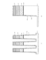
続いて、図9に示すように、フォトレジスト15を塗布した後、フォトリソグラフィ法により周辺回路領域だけを開口する。次いで、図10に示すように、メモリセル領域をレジスト15で覆ったまま、周辺回路領域の第2の素子分離溝24の内面の底部のライナー酸化膜25aを例えばRIE法により異方性エッチングし、シリコン基板1が露出するところまで加工する。この加工により、素子分離溝24の内面の底部のシリコン基板1が露出すると共に、素子分離溝24の内面の側部のうちの最下部(例えば寸法aで示す部分)のシリコン基板1が露出する。そして、素子分離溝24の内面の側部、即ち、上記最下部(寸法a部分)以外の部分は、ライナー酸化膜25aで覆われている。続いて、図11に示すように、アッシング法にて、レジストを剥離する。
Subsequently, as shown in FIG. 9, after applying a
次に、図12に示すように、CVD法により選択的に、周辺回路領域の素子分離溝24内の底部の露出したシリコン基板1上だけに底部酸化膜25cとしてシリコン酸化膜25c(第3の酸化膜、CVD酸化膜)を形成し、メモリセル領域の素子分離溝4内の底部のライナー酸化膜5a(シリコン酸化膜)上にはシリコン酸化膜を形成しないようにする。この場合、CVD法により選択的にシリコン酸化膜を形成する方法としては次に述べる方法がある。例えば低温CVD法により、シリコン酸化膜上とシリコン基板1上とのIncubation time差(即ち、成膜が始まるまでの時間差)を利用して、シリコン基板1上だけにシリコン酸化膜25cを形成し、シリコン酸化膜(ライナー酸化膜5a)上にシリコン酸化膜の成膜が始まる前に成膜を止める方法がある。ここで、周辺回路領域の素子分離溝24内の底部に上記低温CVD法により形成された底部酸化膜(シリコン酸化膜)25cは、塗布膜を酸化膜に置換する熱工程(熱処理)時に体積収縮率が小さい特性を有する酸化膜である。
Next, as shown in FIG. 12, a
続いて、図13に示すように、基板全面(メモリセル領域および周辺回路領域の素子分離溝4、24内)に塗布技術を用いて塗布型酸化膜5b,25bを形成し、メモリセル領域および周辺回路領域の素子分離溝4、24内に塗布型酸化膜5b,25bを埋め込む。この後、塗布型酸化膜5b,25bをシリコン酸化膜に置換する熱処理を実行する。この熱処理においては、低温(例えば400℃程度)水蒸気中で不純物除去および膜の緻密化のために酸化処理を行うと共に、高温(例えば800〜900℃程度)の不活性雰囲気中で熱処理を行うことが好ましい。
Subsequently, as shown in FIG. 13, coating-
上記熱処理時において、塗布型酸化膜5b、25bの体積収縮率が大きいという特性があっても、周辺回路領域の開口幅が大きい素子分離溝24内の底部に低温CVD法により形成された底部酸化膜25c(熱処理時に体積収縮率が小さい特性を有する酸化膜)が埋め込まれることにより、開口幅が大きい素子分離溝24内に埋め込まれる塗布型酸化膜25bの量が少なくなる構成としたので、開口幅が大きい素子分離溝24に大きな応力が作用することがなくなり、結晶欠陥が発生することを防止できる。尚、メモリセル領域の素子分離溝4内の塗布型酸化膜5bについては、素子分離溝4の開口幅が狭いので、熱処理時に塗布型酸化膜5bの体積収縮率が大きいという特性があっても問題は発生しない。
Even when the
この後は、工程等を図示しないが、CMP(chemical mechanical polishing)を用いてシリコン窒化膜14が露出するまで平坦化を行って素子分離絶縁膜5を形成し、更に、浮遊ゲート電極FG(多結晶シリコン層8)間の素子分離絶縁膜5を落とし込む。そして、多結晶シリコン層8上に残っているシリコン窒化膜14を例えばウエットエッチングで選択的にエッチングして除去する。続いて、露出した多結晶シリコン層8および素子分離絶縁膜5の表面に、電極間絶縁膜9を周知のプロセスにより形成する。次いで、電極間絶縁膜9上にCVD法を用いて導電層10(制御ゲート電極CG)となるドープト多結晶シリコン層を形成する。
Thereafter, although not shown in the drawings, the element
更に、周知のプロセスにより、電極分離用の溝17(図3(a)参照)を形成し、複数のゲート構造を得る。次いで、溝17の内底部のシリコン基板1の表面に、イオン注入法を用いて不純物をドーピングし、拡散層6を形成する。次に、溝17内に、セルゲート間絶縁膜としてメモリセル間絶縁膜11を形成した後、平坦化し、落とし込む。そして、多結晶シリコン層(導電層)10の上部にニッケルシリサイド(NiSi)層10bを形成した後、図3(a)に示すように、層間絶縁膜12を形成する。更に、周知の技術を用いて配線等(図示しない)を形成する。
Further, a
上記した構成の本実施形態においては、周辺回路領域の開口幅が大きい素子分離溝24内の底部にCVD法により選択的に底部酸化膜25c、即ち、熱処理時に体積収縮率が小さい特性を有する酸化膜を形成し、開口幅が大きい素子分離溝24内に埋め込まれる塗布型酸化膜25bの量が少なくなるように構成したので、上記熱処理時において、塗布型酸化膜25bの体積収縮率が大きいという特性があっても、開口幅が大きい素子分離溝24に大きな応力が作用することがなくなり、結晶欠陥の発生を防止することができる。尚、メモリセル領域の開口幅が狭い素子分離溝4内は、塗布型酸化膜5bが埋め込まれる構成となるので、ライン曲がり(Line Bending)の発生を防止することができる。
In the present embodiment having the above-described configuration, the
(第2実施形態)
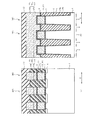
図14および図15は、第2実施形態を示す。尚、第1実施形態と同一構成には、同一符号を付している。この第2実施形態においては、図14に示すように、周辺回路領域の素子分離溝24の内面のうちの側部の下部に、上記側部の下部以外の部分27の傾斜角度Aよりも小さい傾斜角度Bの傾斜部28を形成した。この場合、シリコン基板1をRIE法によりエッチングして素子分離溝4、24を形成する工程において、エッチングステップ、即ち、エッチング条件(加工条件)を変えることにより、上記傾斜部28を形成することが可能である。
(Second Embodiment)
14 and 15 show a second embodiment. In addition, the same code | symbol is attached | subjected to the same structure as 1st Embodiment. In the second embodiment, as shown in FIG. 14, the inclination angle A of the
そして、周辺回路領域の素子分離溝24の内面の底部のライナー酸化膜25aをRIE法によりエッチングしてシリコン基板1を露出させる工程において、傾斜部28の表面上のライナー酸化膜25aもエッチングされることから、傾斜部28の表面部分のシリコン基板1も露出するようになる(図15参照)。
Then, in the step of etching the
次に、CVD法により選択的に、周辺回路領域の素子分離溝24内の底部の露出したシリコン基板1上にだけ底部酸化膜(第3の酸化膜、CVD酸化膜、シリコン酸化膜)25cを形成する工程において、上記傾斜部28の表面部分のシリコン基板1も露出しているから、この露出している部分上にも上記底部酸化膜(第3の酸化膜、CVD酸化膜、シリコン酸化膜)25cが形成される。この場合、素子分離溝24内の底部のシリコン基板1に加えて傾斜部28の表面部分のシリコン基板1も露出しているから、CVD法の成膜時間を、第2実施形態と前記第1実施形態とで同じ時間に設定しても、第2実施形態で形成されるシリコン酸化膜25cの高さ寸法h2は、第1実施形態で形成されるシリコン酸化膜25cの高さ寸法h1(図13参照)よりも高くなる。
Next, a bottom oxide film (third oxide film, CVD oxide film, silicon oxide film) 25c is selectively formed only on the
そして、上述した以外の第2実施形態の構成は、第1実施形態の構成と同じ構成となっている。従って、第2実施形態においても、第1実施形態とほぼ同じ作用効果を得ることができる。特に、第2実施形態では、周辺回路領域の素子分離溝24の内面のうちの側部の下部に傾斜部28を形成し、周辺回路領域の素子分離溝24内の底部および傾斜部28の露出したシリコン基板1上に底部酸化膜25cを形成するように構成したので、素子分離溝24内に形成される底部酸化膜25c(CVD酸化膜)の量が多くなり、素子分離溝24内に埋め込まれる塗布型酸化膜25bの量を少なくすることが可能になる。従って、第2実施形態によれば、熱処理時に開口幅が大きい素子分離溝24に大きな応力が作用することをより一層抑止することができ、結晶欠陥の発生をより一層防止できる。
The configurations of the second embodiment other than those described above are the same as the configurations of the first embodiment. Therefore, in the second embodiment, substantially the same operational effects as in the first embodiment can be obtained. In particular, in the second embodiment, the
(その他の実施形態)
以上説明した複数の実施形態に加えて以下のような構成を採用しても良い。
上記した各実施形態では、NAND型フラッシュメモリ装置に適用したが、他の半導体装置、即ち、開口幅の大きい素子分離溝を塗布型酸化膜で埋め込む構造を有する半導体装置に適用しても良い。
(Other embodiments)
In addition to the plurality of embodiments described above, the following configurations may be adopted.
In each of the embodiments described above, the present invention is applied to the NAND flash memory device. However, the present invention may be applied to other semiconductor devices, that is, semiconductor devices having a structure in which an element isolation trench having a large opening width is embedded with a coating type oxide film.
本発明のいくつかの実施形態を説明したが、これらの実施形態は、例として提示したものであり、発明の範囲を限定することは意図していない。これら新規な実施形態は、その他の様々な形態で実施されることが可能であり、発明の要旨を逸脱しない範囲で、種々の省略、置き換え、変更を行うことができる。これら実施形態やその変形は、発明の範囲や要旨に含まれるとともに、特許請求の範囲に記載された発明とその均等の範囲に含まれる。 Although several embodiments of the present invention have been described, these embodiments are presented by way of example and are not intended to limit the scope of the invention. These novel embodiments can be implemented in various other forms, and various omissions, replacements, and changes can be made without departing from the scope of the invention. These embodiments and modifications thereof are included in the scope and gist of the invention, and are included in the invention described in the claims and the equivalents thereof.
図面中、1はシリコン基板(半導体基板)、2はSTI、3は活性領域、4は素子分離溝(第1の素子分離溝)、5は素子分離絶縁膜、5aはライナー酸化膜(第1の酸化膜)、5bは塗布型酸化膜(第1の塗布型酸化膜)、13はシリコン窒化膜、14はシリコン酸化膜、22はSTI、23は活性領域、24は素子分離溝(第2の素子分離溝)、25は素子分離絶縁膜、25aはライナー酸化膜(第2の酸化膜)、25bは塗布型酸化膜(第2の塗布型酸化膜)、25cはシリコン酸化膜(第3の酸化膜)、26はゲート絶縁膜、28は傾斜部である。 In the drawings, 1 is a silicon substrate (semiconductor substrate), 2 is STI, 3 is an active region, 4 is an element isolation trench (first element isolation trench), 5 is an element isolation insulating film, and 5a is a liner oxide film (first 5b is a coating type oxide film (first coating type oxide film), 13 is a silicon nitride film, 14 is a silicon oxide film, 22 is an STI, 23 is an active region, and 24 is an element isolation groove (second Element isolation trench), 25 is an element isolation insulating film, 25a is a liner oxide film (second oxide film), 25b is a coating type oxide film (second coating type oxide film), and 25c is a silicon oxide film (third layer). , 26 is a gate insulating film, and 28 is an inclined portion.
Claims (5)
前記半導体基板上に設けられ複数のメモリセルが形成されたメモリセル領域と、
前記半導体基板上に設けられた周辺回路領域と、
前記メモリセル領域に形成され、第1の開口幅を有する第1の素子分離溝と、
前記周辺回路領域に形成され、第1の開口幅より大きい第2の開口幅を有する第2の素子分離溝と、
前記第1の素子分離溝の内面に形成された第1の酸化膜と、
前記第1の酸化膜上に形成されて前記第1の素子分離溝内に埋め込まれた第1の塗布型酸化膜と、
前記第2の素子分離溝の内面のうちの側部に形成された第2の酸化膜と、
前記第2の素子分離溝の内面のうちの底部上に形成された第3の酸化膜と、
前記第3の酸化膜上に形成されて前記第2の素子分離溝内に埋め込まれた第2の塗布型酸化膜とを備えたことを特徴とする半導体装置。 A semiconductor substrate;
A memory cell region provided on the semiconductor substrate and formed with a plurality of memory cells;
A peripheral circuit region provided on the semiconductor substrate;
A first element isolation trench formed in the memory cell region and having a first opening width;
A second element isolation trench formed in the peripheral circuit region and having a second opening width larger than the first opening width;
A first oxide film formed on the inner surface of the first element isolation trench;
A first coating type oxide film formed on the first oxide film and embedded in the first element isolation trench;
A second oxide film formed on a side portion of the inner surface of the second element isolation trench;
A third oxide film formed on the bottom of the inner surface of the second element isolation trench;
A semiconductor device comprising: a second coating type oxide film formed on the third oxide film and embedded in the second element isolation trench.
前記第2の素子分離溝の内面のうちの前記底部および前記傾斜部上に前記第3の酸化膜が形成されていることを特徴とする請求項1記載の半導体装置。 Formed at a lower portion of a side portion of the inner surface of the second element isolation groove, and having an inclined portion having an inclination angle smaller than an inclination angle of a portion other than the lower portion of the side portion,
2. The semiconductor device according to claim 1, wherein the third oxide film is formed on the bottom portion and the inclined portion of the inner surface of the second element isolation trench.
前記ゲート絶縁膜上に浮遊ゲート電極用の導電層を形成する工程と、
前記導電層、前記ゲート絶縁膜および前記半導体基板を加工して、メモリセル領域に第1の開口幅を有する第1の素子分離溝を形成し、周辺回路領域に第1の開口幅より大きい第2の開口幅を有する第2の素子分離溝を形成する工程と、
前記第1の素子分離溝の内面、前記第2の素子分離溝の内面、前記ゲート絶縁膜の側部、前記導体層の側部および前記導体層の上面に酸化膜を形成する工程と、
前記酸化膜上にレジストを形成する工程と、
前記レジストにおける前記周辺回路領域を開口する工程と、
前記周辺回路領域の前記第2の素子分離溝の底部の前記酸化膜を加工して前記底部の半導体基板を露出させる工程と、
前記レジストを剥離する工程と、
前記第2の素子分離溝の底部の半導体基板が露出している部分上にCVD法により選択的にCVD酸化膜を形成する工程と、
前記酸化膜および前記CVD酸化膜の上に塗布型酸化膜を形成し、前記第1の素子分離溝および前記第2の素子分離溝を埋め込む工程と
を備えたことを特徴とする半導体装置の製造方法。 Forming a gate insulating film on the semiconductor substrate;
Forming a conductive layer for a floating gate electrode on the gate insulating film;
The conductive layer, the gate insulating film, and the semiconductor substrate are processed to form a first element isolation trench having a first opening width in the memory cell region, and a first larger than the first opening width in the peripheral circuit region. Forming a second element isolation trench having an opening width of 2;
Forming an oxide film on an inner surface of the first element isolation groove, an inner surface of the second element isolation groove, a side portion of the gate insulating film, a side portion of the conductor layer, and an upper surface of the conductor layer;
Forming a resist on the oxide film;
Opening the peripheral circuit region in the resist;
Processing the oxide film at the bottom of the second element isolation trench in the peripheral circuit region to expose the semiconductor substrate at the bottom;
Removing the resist;
Selectively forming a CVD oxide film by a CVD method on a portion where the semiconductor substrate at the bottom of the second element isolation trench is exposed;
Forming a coating-type oxide film on the oxide film and the CVD oxide film, and embedding the first element isolation groove and the second element isolation groove. Method.
前記第2の素子分離溝の底部の前記酸化膜を加工して前記底部の半導体基板を露出させる工程において、前記傾斜部の表面部分の前記半導体基板を前記第2の酸化膜から露出させ、
前記CVD酸化膜を形成する工程において、前記傾斜部の表面部分の前記半導体基板が露出している部分上にも前記CVD酸化膜を形成するように構成したことを特徴とする請求項4記載の半導体装置の製造方法。 In the step of forming the second element isolation groove, an inclined part having an inclination angle smaller than an inclination angle of a part other than the lower part of the side part at a lower part of the side part of the inner surface of the second element isolation groove. Form the
In the step of processing the oxide film at the bottom of the second element isolation trench to expose the semiconductor substrate at the bottom, the semiconductor substrate at the surface portion of the inclined portion is exposed from the second oxide film,
5. The CVD oxide film according to claim 4, wherein in the step of forming the CVD oxide film, the CVD oxide film is also formed on a portion of the surface portion of the inclined portion where the semiconductor substrate is exposed. A method for manufacturing a semiconductor device.
Priority Applications (2)
| Application Number | Priority Date | Filing Date | Title |
|---|---|---|---|
| JP2010281649A JP2012129453A (en) | 2010-12-17 | 2010-12-17 | Semiconductor device and method of manufacturing semiconductor device |
| US13/325,370 US20120153374A1 (en) | 2010-12-17 | 2011-12-14 | Semiconductor device and method of manufacturing the same |
Applications Claiming Priority (1)
| Application Number | Priority Date | Filing Date | Title |
|---|---|---|---|
| JP2010281649A JP2012129453A (en) | 2010-12-17 | 2010-12-17 | Semiconductor device and method of manufacturing semiconductor device |
Publications (1)
| Publication Number | Publication Date |
|---|---|
| JP2012129453A true JP2012129453A (en) | 2012-07-05 |
Family
ID=46233254
Family Applications (1)
| Application Number | Title | Priority Date | Filing Date |
|---|---|---|---|
| JP2010281649A Pending JP2012129453A (en) | 2010-12-17 | 2010-12-17 | Semiconductor device and method of manufacturing semiconductor device |
Country Status (2)
| Country | Link |
|---|---|
| US (1) | US20120153374A1 (en) |
| JP (1) | JP2012129453A (en) |
Families Citing this family (2)
| Publication number | Priority date | Publication date | Assignee | Title |
|---|---|---|---|---|
| TWI555179B (en) * | 2015-02-02 | 2016-10-21 | 力晶科技股份有限公司 | Method of manufacturing isolation structure and non-volatile memory with the isolation structure |
| TWI774007B (en) * | 2020-06-16 | 2022-08-11 | 華邦電子股份有限公司 | Patterning method |
Family Cites Families (6)
| Publication number | Priority date | Publication date | Assignee | Title |
|---|---|---|---|---|
| US7192891B2 (en) * | 2003-08-01 | 2007-03-20 | Samsung Electronics, Co., Ltd. | Method for forming a silicon oxide layer using spin-on glass |
| JP2005332885A (en) * | 2004-05-18 | 2005-12-02 | Toshiba Corp | Nonvolatile semiconductor memory device and its manufacturing method |
| US7691722B2 (en) * | 2006-03-14 | 2010-04-06 | Micron Technology, Inc. | Isolation trench fill using oxide liner and nitride etch back technique with dual trench depth capability |
| KR100745934B1 (en) * | 2006-06-30 | 2007-08-02 | 주식회사 하이닉스반도체 | Semiconductor device and method for forming the same |
| KR20090097737A (en) * | 2008-03-12 | 2009-09-16 | 삼성전자주식회사 | Nonvolatile memory device having buried shield plate and method for manufacturing the same |
| KR101062293B1 (en) * | 2008-11-14 | 2011-09-05 | 주식회사 하이닉스반도체 | Semiconductor device and manufacturing method thereof |
-
2010
- 2010-12-17 JP JP2010281649A patent/JP2012129453A/en active Pending
-
2011
- 2011-12-14 US US13/325,370 patent/US20120153374A1/en not_active Abandoned
Also Published As
| Publication number | Publication date |
|---|---|
| US20120153374A1 (en) | 2012-06-21 |
Similar Documents
| Publication | Publication Date | Title |
|---|---|---|
| US7800155B2 (en) | Semiconductor device | |
| US7906396B1 (en) | Flash memory and method of fabricating the same | |
| JP3917063B2 (en) | Semiconductor device and manufacturing method thereof | |
| JP5091452B2 (en) | Manufacturing method of semiconductor device | |
| US20090047777A1 (en) | Semiconductor device and method of manufacturing the same | |
| JP2009026802A (en) | Manufacturing method of semiconductor device, and semiconductor device | |
| JP2010087160A (en) | Method of manufacturing nonvolatile semiconductor storage, and nonvolatile semiconductor storage | |
| JP2010080853A (en) | Nonvolatile semiconductor storage device, and method for manufacturing the same | |
| US20080087981A1 (en) | Semiconductor device and method of fabricating the same | |
| JP2010040753A (en) | Method of manufacturing nonvolatile semiconductor storage device | |
| JP5330440B2 (en) | Manufacturing method of semiconductor device | |
| JP2012199277A (en) | Method for manufacturing electronic components | |
| JP2006278967A (en) | Semiconductor device and manufacturing method | |
| JP2010087159A (en) | Nonvolatile semiconductor storage and method of manufacturing the same | |
| JP2009289813A (en) | Production method of non-volatile semiconductor memory device | |
| KR100951981B1 (en) | Semiconductor device and method for manufacturing the same | |
| JP2012129453A (en) | Semiconductor device and method of manufacturing semiconductor device | |
| JP2014187132A (en) | Semiconductor device | |
| US7592036B2 (en) | Method for manufacturing NAND flash memory | |
| JP2008098503A (en) | Semiconductor device and its manufacturing method | |
| JP2013065775A (en) | Semiconductor device and semiconductor device manufacturing method | |
| JP2012049365A (en) | Manufacturing method of semiconductor device | |
| JP2013143482A (en) | Semiconductor device and semiconductor device manufacturing method | |
| JP2009252773A (en) | Nonvolatile semiconductor memory device and manufacturing method thereof | |
| JP2013026331A (en) | Manufacturing method of nonvolatile semiconductor memory device |