JP2004287767A - Noncontact communication type information carrier - Google Patents
Noncontact communication type information carrier Download PDFInfo
- Publication number
- JP2004287767A JP2004287767A JP2003078180A JP2003078180A JP2004287767A JP 2004287767 A JP2004287767 A JP 2004287767A JP 2003078180 A JP2003078180 A JP 2003078180A JP 2003078180 A JP2003078180 A JP 2003078180A JP 2004287767 A JP2004287767 A JP 2004287767A
- Authority
- JP
- Japan
- Prior art keywords
- coil
- semiconductor chip
- booster
- information carrier
- type information
- Prior art date
- Legal status (The legal status is an assumption and is not a legal conclusion. Google has not performed a legal analysis and makes no representation as to the accuracy of the status listed.)
- Granted
Links
Images


Abstract
Description
【0001】
【発明の属する技術分野】
本発明は、アンテナコイルが一体形成された半導体チップとブースタコイルとを有する非接触通信式情報担体に係り、特に、アンテナコイル及びブースタコイルの形状と配列とに関する。
【0002】
【従来の技術】
従来より、絶縁部材内に半導体チップと当該半導体チップの端子部に電気的に接続されたアンテナコイルとを備え、リーダライタからの電力の受給及びリーダライタとの間の信号の送受信を電磁波を用いて非接触で行う非接触式の情報担体が知られている。この種の情報担体としては、その外形により、カード形、コイン形、ボタン形又はタグ形などがある。
【0003】
従来、この種の情報担体としては、アンテナコイルを絶縁部材にパターン形成したもの、或いは、巻線からなるアンテナコイルを絶縁部材に担持したものが用いられているが、近年に至って、アンテナコイルと半導体チップとの接続点の保護処理や防湿対策が不要で安価に作成できること、及び絶縁部材に曲げやねじれ等のストレスが作用した場合にもコイルに断線を生じることがなく耐久性に優れることなどから、半導体チップ自体にアンテナコイルが一体形成された半導体チップを絶縁部材に搭載したものが提案されている。
【0004】
アンテナコイルを半導体チップに一体形成した場合、アンテナコイルを絶縁部材にパターン形成したり、巻線からなるアンテナコイルを絶縁部材に担持する場合に比べて、コイルの巻径や導体幅が小さくなり、巻数についても自ずと限界があるため、リーダライタとの間の通信距離を大きくすることが困難で、必要な通信距離を確保することできない場合がある。そこで、従来より、半導体チップに一体形成されたアンテナコイルとリーダライタに備えられたアンテナコイルとの間に、各アンテナコイル間の電磁誘導結合を強化するため、少なくとも1つの巻数を持ちその断面積がほぼデータ媒体装置(絶縁部材)の寸法を有する第2の導体ループと、少なくとも1つの巻数を持ちその断面積が半導体チップに接続された第1の導体ループ(半導体チップに一体形成されたアンテナコイル)の寸法をほぼ有する第3のループとを備え、第1及び第3の導体ループをほぼ同心的に配置し、第1及び第2の導体ループを第3のループを介して互いに誘導結合する技術が提案されている(例えば、特許文献1参照。)。
【0005】
なお、本明細書においては、このアンテナコイル間の電磁誘導結合を強化するための導体ループを、「ブースタコイル」という。
【0006】
【特許文献1】
特開平8−532904号公報(図1)
【0007】
【発明が解決しようとする課題】
前記特許文献に記載の技術によれば、ブースタコイルを介して半導体チップに一体形成されたアンテナコイルとリーダライタに備えられたアンテナコイルとが互いに電磁誘導結合されるので、各アンテナコイル間の電磁誘導結合が強化され、非接触通信式情報担体とリーダライタとの間の通信距離の延長を図ることができる。
【0008】
しかしながら、前記特許文献に記載の技術は、半導体チップに一体形成されたアンテナコイル(第1の導体ループ)とブースタコイルに形成された第3の導体ループとをほぼ同心の所定の位置関係に配置することによって各導体ループ間の良好な電磁誘導結合を実現するというものであるので、各導体ループの配設位置を厳密に規制しないと良好な電磁誘導結合が得られず、非接触通信式情報担体とリーダライタとの間の通信距離にばらつきが生じやすいという問題がある。また、各導体ループの配設位置を厳密に規制しなくてはならないことから、絶縁部材に対する半導体チップの搭載工程が複雑化し、非接触通信式情報担体が高コスト化するという問題がある。
【0009】
本発明は、かかる従来技術の不備を解決するためになされたものであって、その課題は、安価に製造できてリーダライタとの間の通信特性が安定な非接触通信式情報担体を提供することにある。
【0010】
【課題を解決するための手段】
本発明は、前記の課題を解決するため、第1に、アンテナコイルが一体形成された半導体チップと、前記半導体チップに一体形成されたアンテナコイル及びリーダライタに備えられたアンテナコイルと電磁誘導結合するブースタコイルと、これら半導体チップ及びブースタコイルを担持する絶縁部材とを備えた非接触通信式情報担体において、前記ブースタコイル及び前記半導体チップに一体形成されたアンテナコイルの双方を内周部にコイル非形成領域を有する渦巻き状に形成し、前記絶縁基板の平面方向から見たとき、前記ブースタコイルのコイル非形成領域と前記半導体チップに一体形成されたアンテナコイルのコイル非形成領域とが少なくとも一部において重なり合うように前記半導体チップとブースタコイルとを配置するという構成にした。
【0011】
このように、ブースタコイルのコイル非形成領域と半導体チップに一体形成されたアンテナコイルのコイル非形成領域とが少なくとも一部において重なり合うように半導体チップとブースタコイルとを配置すると、ブースタコイルの巻数及びアンテナコイルの巻数に関係なくブースタコイルのコイル非形成領域内にアンテナコイルを構成する各ターンの導体を少なくともその一部において露出させることができるので、当該露出部分において磁気的な干渉のない電磁誘導結合が行われ、ブースタコイルとアンテナコイルとの電磁誘導結合を強化することができて、非接触通信式情報担体とリーダライタとの通信距離の延長を図ることができる。また、各コイル非形成領域が少なくとも一部において重なり合うように配置されている限り、半導体チップとブースタコイルとの配置が若干ずれたとしてもブースタコイルとアンテナコイルとの間の良好な電磁誘導結合を維持することができるので、絶縁部材に対する半導体チップの搭載工程を簡略化できて非接触通信式情報担体を低コスト化できると共に、非接触通信式情報担体とリーダライタとの間の通信距離のばらつきを小さくすることができる。
【0012】
また、本発明は、前記の課題を解決するため、第2に、前記第1の課題解決手段に記載の非接触通信式情報担体において、前記ブースタコイル及び前記半導体チップに一体形成されたアンテナコイルの双方を内周部にコイル非形成領域を有する矩形渦巻き状に形成し、前記ブースタコイルの角隅部に前記半導体チップを配置するという構成にした。
【0013】
このように、矩形渦巻き状に形成されたブースタコイルの角隅部に半導体チップを配置すると、ブースタコイルと半導体チップに一体形成されたアンテナコイルとの電磁誘導結合をより一層強化することができるので、その結果、非接触通信式情報担体とリーダライタとの間のより一層の通信距離の延長を図ることができる。
【0014】
また、本発明は、前記の課題を解決するため、第3に、前記第1の課題解決手段に記載の非接触通信式情報担体において、前記ブースタコイル及び前記半導体チップに一体形成されたアンテナコイルの双方を内周部にコイル非形成領域を有する矩形渦巻き状に形成し、前記ブースタコイルの側辺部に沿って前記半導体チップを配置するという構成にした。
【0015】
このように、矩形渦巻き状に形成されたブースタコイルの側辺部に沿って半導体チップを配置すると、ブースタコイルの側辺に沿う方向に関して半導体チップの設定位置の自由度を高めることができるので、絶縁部材に対する半導体チップの搭載工程を簡略化できて非接触通信式情報担体を低コスト化することができる。
【0016】
また、本発明は、前記の課題を解決するため、第4に、前記第1の課題解決手段に記載の非接触通信式情報担体において、前記絶縁基板上に1つのブースタコイルを形成し、当該1つのブースタコイルに対して複数個の前記半導体チップを配置するという構成にした。
【0017】
このように、絶縁基板上に1つのブースタコイルを形成すると、絶縁部材に複数個のブースタコイルを形成する場合に比べて1つのブースタコイルに対して複数個の前記半導体チップを配置すると、各半導体チップごとに異なる機能を発揮させ、異なる用途に適用することができるので、非接触通信式情報担体の多機能化及び多用途化を図ることができる。
【0018】
【発明の実施の形態】
以下、本発明に係る非接触通信式情報担体の一実施形態例を、図1乃至図8に基づいて説明する。図1は実施形態例に係る非接触通信式情報担体に備えられたブースタコイルと半導体チップとの配列を示す平面図、図2は図1のA−A断面図、図3はブースタコイルと半導体チップに一体形成されたアンテナコイルとの配列を模式的に示す図、図4はブースタコイルと半導体チップに一体形成されたアンテナコイルとの配列を模式的に示す図、図5は絶縁部材の表面図、図6は絶縁部材の裏面図、図7は半導体チップの平面図、図8は本例の非接触通信式情報担体に備えられたブースタコイルの等価回路図である。
【0019】
図1及び図2に示すように、本例の非接触通信式情報担体は、アンテナコイル1が一体形成された半導体チップ2と、ブースタコイル3及び静電容量を形成する導体膜4a,4b,5a,5bが形成された絶縁部材6と、これら半導体チップ2及び絶縁部材6を一体にケーシングする基体7とからなる。
【0020】
半導体チップ2は、図7に示すように、入出力端子2aの形成面に、ポリイミド樹脂膜等からなる絶縁層2bを介して、内周部にコイル非形成領域1aを有する矩形渦巻き状のアンテナコイル1を一体に形成してなる。アンテナコイル1は、フォトレジスト法、即ち、半導体チップ2(より実際的には、個々の半導体チップに分割される以前の完成ウエハ)の絶縁層形成面に、入出力端子形成部を除いてフォトレジスト層を均一の厚さに形成し、このフォトレジスト層に所要のコイルパターンを露光・現像した後、フォトレジスト層をマスクとして半導体チップ2の絶縁層2b上に導電性金属材料をスパッタリング又は真空蒸着し、しかる後に、フォトレジスト層を除去して入出力端子2aの形成面に導電性金属材料からなるコイルパターンを形成するといった方法で形成することができる。なお、コイルパターンの電気抵抗を減少するため、導電性金属膜の表面に銅のめっき層を形成することもできる。
【0021】
なお、図7の例では、アンテナコイル1が複数のターン数を有する矩形渦巻き状に形成されているが、当該アンテナコイル1のターン数や平面形状はこれに限定されるものではない。即ち、ターン数に関しては、1ターン以上の任意のターン数とすることができ、平面形状に関しては、角部に斜線状又は円弧状の面取りが施された矩形や円形など、任意の形状に形成できる。
【0022】
ブースタコイル3は、図5に示すように、絶縁部材6の表面側に、内周部にコイル非形成領域3aを有する矩形渦巻き状に形成される。このブースタコイル3は、基体7内に収まる範囲でなるべく大きく形成され、その両端部には静電容量を形成する導体膜4a,4bがそれぞれ接続されている。
【0023】
なお、図5の例では、ブースタコイル3が複数のターン数を有する矩形渦巻き状に形成されているが、ブースタコイル3のターン数や平面形状はこれに限定されるものではなく、前述のアンテナコイル1と同様に、任意のターン数及び形状に形成することができる。
【0024】
半導体チップ2は、図1乃至図4に示すように、アンテナコイル1を絶縁部材6側に向け、かつ、アンテナコイル1のコイル非形成領域1aとブースタコイル3のコイル非形成領域3aとが一部において重なり合うようにして、ブースタコイル3の角隅部に設定される。
【0025】
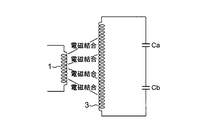
静電容量を形成する導体膜4aと5a及び4bと5bは、絶縁部材6の表面及び裏面に対向に形成される。また、絶縁部材6の表面側に形成された静電容量を形成する導体膜4a,4bは、前記したように、ブースタコイル3を介して電気的に接続され、絶縁部材6の裏面側に形成された静電容量を形成する導体膜5a,5bは、図6に示すように、導線5cを介して電気的に接続される。したがって、前記ブースタコイル3は、相対向に配置された静電容量を形成する導体膜4aと5a及び4bと5bを介してその両端部で容量結合されており、図8に模式的に示すように、両端に導体膜4aと5aとで形成される静電容量Caと導体膜4bと5bとで形成される静電容量Cbとが接続されたブースタコイル3が得られる。各導体膜4a,5a,4b,5bの面積は、前記2個の静電容量Ca,Cbの直列インピーダンスが、半導体チップ2に一体形成されたアンテナコイル1及びブースタコイル3を含む系において、アンテナコイル1の両端に最大電圧が得られるように調整される。
【0026】
前記ブースタコイル3及び静電容量を形成する導体膜4a,5a,4b,5bは、絶縁部材6の片面に形成された均一厚さの導電性金属層にエッチングを施して所要のコイルパターンを形成するエッチング法や、絶縁部材6の片面に導電性インクを用いて所要の導電パターンを印刷形成する印刷法などをもって形成することができる。
【0027】
絶縁部材6は、所要の誘電率と剛性とをもった絶縁材料をもって形成される。絶縁部材6を構成するに好適な絶縁材料としては、一例として、ガラスエポキシ樹脂、ポリイミド樹脂、ポリアミド樹脂、ポリエチレンテレフタレート樹脂(以下、PETと略称する。)又は塩化ビニル樹脂などを挙げることができる。
【0028】
基体7は、カバーシート8と接着剤層9とをもって構成される。このうち、カバーシート8は、紙やプラスチックシートなど、任意のシート状材料をもって形成することができるが、廃棄しても分解し、焼却してもダイオキシン等の有害物質を発生しないことから、紙をもって形成することが最も好ましい。カバーシート材料としてプラスチックシートを用いる場合には、焼却してもダイオキシン等の有害物質を発生しないことから、PETのような塩素を含まないプラスチックシートを用いることが特に好ましい。一方、接着剤層9を構成する接着剤としては、硬化後に所要の硬度を有する任意の接着剤を用いることができるが、ブースタコイル1、アンテナコイル3及び半導体チップ4の保護効果を高めるため、例えばエポキシ樹脂のように吸湿性の低い樹脂材料を用いることが特に好ましい。
【0029】
本例の非接触通信式情報担体は、半導体チップ2に一体形成されたアンテナコイル1のコイル非形成領域1aとブースタコイル3のコイル非形成領域3aとが一部において重なり合うように半導体チップ2とブースタコイル3とを配置したので、図4に模式的に示すように、アンテナコイル1の巻数及びブースタコイル3の巻数に関係なくブースタコイル3のコイル非形成領域3a内にアンテナコイル1を構成する各ターンの導体の1部を露出させることができる。そして、当該露出部分においては、ブースタコイル3より放射される磁力線に干渉を生じないので、最適な電磁誘導結合が行われ、非接触通信式情報担体とリーダライタとの電磁誘導結合を強化することができる。アンテナコイル1からブースタコイル3への送信時にも同様の理由により最適な電磁誘導結合が行われる。また、本例の非接触通信式情報担体は、各コイル非形成領域1a,3aが一部において重なり合うように配置されている限り、半導体チップ2とブースタコイル3との配置が若干ずれたとしてもアンテナコイル1とブースタコイル3との間の良好な電磁誘導結合を維持することができるので、絶縁部材6に対する半導体チップ2の搭載工程を簡略化できて非接触通信式情報担体を低コスト化できると共に、非接触通信式情報担体とリーダライタとの間の通信距離のばらつきを小さくすることができる。さらに、本例の非接触通信式情報担体は、矩形渦巻き状に形成されたブースタコイル3の角隅部に半導体チップ2を配置したので、アンテナコイル1とブースタコイル3との電磁誘導結合をより一層強固なものとすることができる。
【0030】
以下、本発明の他の実施形態について列挙する。なお、図9はブースタコイル3に対するアンテナコイル1の他の配列例を模式的に示す図である。
【0031】
(1)前記実施形態例においては、アンテナコイル1のコイル非形成領域1aとブースタコイル3のコイル非形成領域3aとが一部において重なり合うように半導体チップ2とブースタコイル3とを配置したが、本発明の要旨はこれに限定されるものではなく、図9(a)に示すように、アンテナコイル1のコイル非形成領域1aとブースタコイル3のコイル非形成領域3aとが完全に重なり合うように半導体チップ2とブースタコイル3とを配置することもできる。
【0032】
(2)前記実施形態例においては、ブースタコイル3の角隅部に半導体チップ2を配置したが、本発明の要旨はこれに限定されるものではなく、図9(b)に示すように、ブースタコイル3の側辺部に沿って半導体チップ2を配置することもできる。このように、ブースタコイル3の側辺部に沿って半導体チップ2を配置すると、ブースタコイル3の側辺に沿う方向に対する半導体チップ2の設定位置の自由度を高めることができるので、絶縁部材6に対する半導体チップ2の搭載工程を簡略化でき、非接触通信式情報担体を低コスト化することができる。
【0033】
(3)前記実施形態例においては、1枚の絶縁基板6上に半導体チップ2を1つのみ搭載したが、本発明の要旨はこれに限定されるものではなく、図9(c)に示すように、1枚の絶縁基板6上に複数個の半導体チップ2を搭載することもできる。このように、1枚の絶縁基板6上に複数個の半導体チップ2を搭載すると、各半導体チップ2ごとに異なる機能を発揮させ、異なる用途に適用することができるので、非接触通信式情報担体の多機能化及び多用途化を図ることができる。
【0034】
(4)前記実施形態例においては、絶縁基板6に静電容量を形成する導体膜4a,5a,4b,5bを形成したが、本発明の要旨はこれに限定されるものではなく、チップコンデンサ等のチップ部品を絶縁基板6上に形成されたブースタコイル3に接続することもできる。
【0035】
【発明の効果】
以上説明したように、本発明の非接触通信式情報担体は、半導体チップに一体形成されたアンテナコイルのコイル非形成領域とブースタコイルのコイル非形成領域とが少なくとも一部において重なり合うように半導体チップとブースタコイルとを配置したので、アンテナコイルの巻数及びブースタコイルの巻数に関係なくブースタコイルのコイル非形成領域内にアンテナコイルを構成する各ターンの導体の一部を露出させることができ、当該露出部分においてアンテナコイルとブースタコイルとの間で磁気的な干渉のない最適な電磁誘導結合を行うことができて、非接触通信式情報担体とリーダライタとの電磁誘導結合を強化することができる。また、本発明の非接触通信式情報担体は、アンテナコイルのコイル非形成領域とブースタコイルのコイル非形成領域とが少なくとも一部において重なり合うように配置されている限り、半導体チップとブースタコイルとの配置が若干ずれたとしてもアンテナコイルとブースタコイルとの間の良好な電磁誘導結合を維持することができるので、絶縁部材に対する半導体チップの搭載工程を簡略化できて非接触通信式情報担体を低コスト化できると共に、非接触通信式情報担体とリーダライタとの間の通信距離のばらつきを小さくすることができる。
【図面の簡単な説明】
【図1】実施形態例に係る非接触通信式情報担体に備えられたブースタコイルと半導体チップとの配列を示す平面図である。
【図2】図1のA−A断面図である。
【図3】ブースタコイルと半導体チップに一体形成されたアンテナコイルとの配列を模式的に示す図である。
【図4】ブースタコイルと半導体チップに一体形成されたアンテナコイルとの配列を模式的に示す図である。
【図5】絶縁部材の表面図である。
【図6】絶縁部材の裏面図である。
【図7】半導体チップの平面図である。
【図8】非接触通信式情報担体に備えられたブースタコイルの等価回路図である。
【図9】ブースタコイルに対する半導体チップの他の配列例を模式的に示す図である。
【符号の説明】
1 アンテナコイル
1a コイル非形成領域
2 半導体チップ
3 ブースタコイル
3a コイル非形成領域
4a,4b,5a,5b 静電容量を形成する導体膜
6 絶縁部材
7 基体
8 カバーシート
9 接着剤層[0001]
TECHNICAL FIELD OF THE INVENTION
The present invention relates to a non-contact communication type information carrier having a semiconductor chip and a booster coil integrally formed with an antenna coil, and more particularly, to a shape and an arrangement of the antenna coil and the booster coil.
[0002]
[Prior art]
Conventionally, a semiconductor chip and an antenna coil electrically connected to a terminal portion of the semiconductor chip are provided in an insulating member, and electromagnetic waves are used to receive power from a reader / writer and transmit / receive signals to / from the reader / writer. A non-contact type information carrier that performs non-contact operation is known. This type of information carrier has a card shape, a coin shape, a button shape, a tag shape, or the like, depending on its outer shape.
[0003]
Conventionally, as this type of information carrier, one in which an antenna coil is formed in a pattern on an insulating member, or one in which an antenna coil formed of a winding is supported on an insulating member has been used. No need to protect the connection point with the semiconductor chip or take measures against moisture proof, it can be made at low cost, and even if stress such as bending or torsion acts on the insulating member, the coil does not break and has excellent durability. Accordingly, a semiconductor chip in which an antenna coil is integrally formed on a semiconductor chip itself is mounted on an insulating member.
[0004]
When the antenna coil is integrally formed on the semiconductor chip, the coil diameter and the conductor width are smaller than when the antenna coil is patterned on an insulating member or the antenna coil formed of a winding is carried on the insulating member, Since the number of turns is naturally limited, it is difficult to increase the communication distance with the reader / writer, and the necessary communication distance may not be secured. Therefore, conventionally, between an antenna coil integrally formed on a semiconductor chip and an antenna coil provided in a reader / writer, at least one winding has a cross-sectional area in order to strengthen electromagnetic induction coupling between the antenna coils. A second conductor loop having substantially the dimensions of a data medium device (insulating member), and a first conductor loop having at least one winding and having a cross-sectional area connected to the semiconductor chip (an antenna integrally formed with the semiconductor chip). A third loop having substantially the dimensions of a coil), wherein the first and third conductor loops are arranged substantially concentrically, and the first and second conductor loops are inductively coupled to each other via the third loop. A technique has been proposed (see, for example, Patent Document 1).
[0005]
In this specification, a conductor loop for enhancing the electromagnetic induction coupling between the antenna coils is referred to as a “booster coil”.
[0006]
[Patent Document 1]
JP-A-8-532904 (FIG. 1)
[0007]
[Problems to be solved by the invention]
According to the technique described in the patent document, the antenna coil integrally formed on the semiconductor chip and the antenna coil provided on the reader / writer are electromagnetically inductively coupled to each other via the booster coil. The inductive coupling is strengthened, and the communication distance between the non-contact communication type information carrier and the reader / writer can be extended.
[0008]
However, the technology described in the above-mentioned patent document arranges an antenna coil (first conductor loop) integrally formed on a semiconductor chip and a third conductor loop formed on a booster coil in a substantially concentric predetermined positional relationship. Therefore, good electromagnetic induction coupling cannot be obtained unless the position of each conductor loop is strictly regulated. There is a problem that the communication distance between the carrier and the reader / writer tends to vary. In addition, since the arrangement position of each conductor loop must be strictly regulated, there is a problem that the mounting process of the semiconductor chip on the insulating member is complicated and the cost of the non-contact communication information carrier is increased.
[0009]
The present invention has been made to solve the deficiencies of the related art, and an object thereof is to provide a non-contact communication information carrier which can be manufactured at low cost and has stable communication characteristics with a reader / writer. It is in.
[0010]
[Means for Solving the Problems]
In order to solve the above-described problems, the present invention firstly provides a semiconductor chip having an antenna coil integrally formed thereon, and an electromagnetic induction coupling with an antenna coil formed integrally with the semiconductor chip and an antenna coil provided in a reader / writer. In a non-contact communication type information carrier provided with a booster coil and an insulating member carrying the semiconductor chip and the booster coil, both the booster coil and the antenna coil formed integrally with the semiconductor chip are coiled on the inner peripheral portion. When formed in a spiral shape having a non-formation area, when viewed from the plane direction of the insulating substrate, at least one of the coil non-formation area of the booster coil and the coil non-formation area of the antenna coil integrally formed with the semiconductor chip is provided. A configuration in which the semiconductor chip and the booster coil are arranged so as to overlap each other. It was.
[0011]
Thus, when the semiconductor chip and the booster coil are arranged such that the coil non-formation region of the booster coil and the coil non-formation region of the antenna coil integrally formed on the semiconductor chip at least partially overlap, the number of turns of the booster coil and Regardless of the number of turns of the antenna coil, the conductor of each turn constituting the antenna coil can be exposed in at least a part thereof in the coil-free area of the booster coil. The coupling is performed, so that the electromagnetic induction coupling between the booster coil and the antenna coil can be strengthened, and the communication distance between the non-contact communication type information carrier and the reader / writer can be extended. In addition, as long as the coil non-forming regions are arranged so as to overlap at least in part, good electromagnetic induction coupling between the booster coil and the antenna coil can be achieved even if the arrangement of the semiconductor chip and the booster coil is slightly shifted. Since it can be maintained, the process of mounting the semiconductor chip on the insulating member can be simplified, the cost of the non-contact communication information carrier can be reduced, and the communication distance between the non-contact communication information carrier and the reader / writer varies. Can be reduced.
[0012]
According to another aspect of the present invention, there is provided a non-contact communication information carrier according to the first aspect, wherein the booster coil and the antenna coil are formed integrally with the semiconductor chip. Are formed in a rectangular spiral shape having a coil non-forming region on the inner peripheral portion, and the semiconductor chip is disposed at a corner of the booster coil.
[0013]
As described above, when the semiconductor chip is arranged at the corner of the booster coil formed in a rectangular spiral shape, the electromagnetic induction coupling between the booster coil and the antenna coil formed integrally with the semiconductor chip can be further enhanced. As a result, the communication distance between the non-contact communication type information carrier and the reader / writer can be further extended.
[0014]
Thirdly, in order to solve the above-mentioned problem, in the non-contact communication type information carrier according to the first problem solving means, an antenna coil integrally formed with the booster coil and the semiconductor chip Are formed in a rectangular spiral shape having a coil non-forming region in the inner peripheral portion, and the semiconductor chip is arranged along the side of the booster coil.
[0015]
By arranging the semiconductor chip along the side of the booster coil formed in a rectangular spiral as described above, the degree of freedom of the setting position of the semiconductor chip in the direction along the side of the booster coil can be increased. The process of mounting the semiconductor chip on the insulating member can be simplified, and the cost of the non-contact communication information carrier can be reduced.
[0016]
Fourth, the present invention provides a contactless communication information carrier according to the first problem solving means, wherein one booster coil is formed on the insulating substrate. A plurality of the semiconductor chips are arranged for one booster coil.
[0017]
As described above, when one booster coil is formed on an insulating substrate, compared to a case where a plurality of booster coils are formed on an insulating member, when a plurality of the semiconductor chips are arranged for one booster coil, Since different functions can be exhibited for each chip and can be applied to different uses, multifunctional and multipurpose noncontact communication information carriers can be achieved.
[0018]
BEST MODE FOR CARRYING OUT THE INVENTION
Hereinafter, an embodiment of a non-contact communication type information carrier according to the present invention will be described with reference to FIGS. FIG. 1 is a plan view showing an arrangement of a booster coil and a semiconductor chip provided on a non-contact communication type information carrier according to an embodiment, FIG. 2 is a sectional view taken along line AA of FIG. 1, and FIG. FIG. 4 is a diagram schematically illustrating an arrangement of an antenna coil integrally formed on a chip, FIG. 4 is a diagram schematically illustrating an arrangement of an antenna coil integrally formed on a semiconductor chip, and FIG. 5 is a surface of an insulating member; FIG. 6 is a rear view of the insulating member, FIG. 7 is a plan view of the semiconductor chip, and FIG. 8 is an equivalent circuit diagram of a booster coil provided in the non-contact communication type information carrier of this embodiment.
[0019]
As shown in FIGS. 1 and 2, the non-contact communication type information carrier of the present embodiment includes a
[0020]
As shown in FIG. 7, the
[0021]
In the example of FIG. 7, the
[0022]
As shown in FIG. 5, the
[0023]
In the example shown in FIG. 5, the
[0024]
As shown in FIGS. 1 to 4, the
[0025]
The
[0026]
The
[0027]
The insulating
[0028]
The
[0029]
The non-contact communication type information carrier of the present example is configured so that the
[0030]
Hereinafter, other embodiments of the present invention will be listed. FIG. 9 is a diagram schematically showing another example of the arrangement of the
[0031]
(1) In the above embodiment, the
[0032]
(2) In the above embodiment, the
[0033]
(3) In the above embodiment, only one
[0034]
(4) In the above embodiment, the
[0035]
【The invention's effect】
As described above, the non-contact communication type information carrier of the present invention is configured such that the semiconductor chip is formed such that the coil-free area of the antenna coil and the coil-free area of the booster coil which are integrally formed on the semiconductor chip at least partially overlap. And the booster coil are arranged, so that a part of the conductor of each turn constituting the antenna coil can be exposed in the coil-free area of the booster coil regardless of the number of turns of the antenna coil and the number of turns of the booster coil. Optimal electromagnetic induction coupling between the antenna coil and the booster coil without magnetic interference can be performed in the exposed portion, and the electromagnetic induction coupling between the non-contact communication type information carrier and the reader / writer can be enhanced. . Further, the non-contact communication type information carrier of the present invention, the semiconductor chip and the booster coil, as long as the coil non-formation area of the antenna coil and the coil non-formation area of the booster coil are arranged so as to at least partially overlap each other. Even if the arrangement is slightly deviated, good electromagnetic induction coupling between the antenna coil and the booster coil can be maintained, so that the process of mounting the semiconductor chip on the insulating member can be simplified and the contactless communication information carrier can be reduced. The cost can be reduced, and the variation in the communication distance between the non-contact communication type information carrier and the reader / writer can be reduced.
[Brief description of the drawings]
FIG. 1 is a plan view showing an arrangement of a booster coil and a semiconductor chip provided on a non-contact communication type information carrier according to an embodiment.
FIG. 2 is a sectional view taken along line AA of FIG.
FIG. 3 is a diagram schematically showing an arrangement of a booster coil and an antenna coil formed integrally with a semiconductor chip.
FIG. 4 is a diagram schematically showing an arrangement of a booster coil and an antenna coil formed integrally with a semiconductor chip.
FIG. 5 is a front view of the insulating member.
FIG. 6 is a rear view of the insulating member.
FIG. 7 is a plan view of a semiconductor chip.
FIG. 8 is an equivalent circuit diagram of a booster coil provided on the non-contact communication type information carrier.
FIG. 9 is a diagram schematically showing another example of the arrangement of the semiconductor chips with respect to the booster coil.
[Explanation of symbols]
REFERENCE SIGNS
Claims (4)
Priority Applications (1)
| Application Number | Priority Date | Filing Date | Title |
|---|---|---|---|
| JP2003078180A JP4034676B2 (en) | 2003-03-20 | 2003-03-20 | Non-contact communication type information carrier |
Applications Claiming Priority (1)
| Application Number | Priority Date | Filing Date | Title |
|---|---|---|---|
| JP2003078180A JP4034676B2 (en) | 2003-03-20 | 2003-03-20 | Non-contact communication type information carrier |
Publications (2)
| Publication Number | Publication Date |
|---|---|
| JP2004287767A true JP2004287767A (en) | 2004-10-14 |
| JP4034676B2 JP4034676B2 (en) | 2008-01-16 |
Family
ID=33292733
Family Applications (1)
| Application Number | Title | Priority Date | Filing Date |
|---|---|---|---|
| JP2003078180A Expired - Fee Related JP4034676B2 (en) | 2003-03-20 | 2003-03-20 | Non-contact communication type information carrier |
Country Status (1)
| Country | Link |
|---|---|
| JP (1) | JP4034676B2 (en) |
Cited By (101)
| Publication number | Priority date | Publication date | Assignee | Title |
|---|---|---|---|---|
| WO2007083574A1 (en) * | 2006-01-19 | 2007-07-26 | Murata Manufacturing Co., Ltd. | Radio ic device and radio ic device part |
| JPWO2006072990A1 (en) * | 2005-01-07 | 2008-06-12 | 富士通株式会社 | Tag device, antenna and portable card |
| JP2008226099A (en) * | 2007-03-15 | 2008-09-25 | Dainippon Printing Co Ltd | Noncontact data carrier device |
| US7764928B2 (en) | 2006-01-19 | 2010-07-27 | Murata Manufacturing Co., Ltd. | Wireless IC device and component for wireless IC device |
| US7762472B2 (en) | 2007-07-04 | 2010-07-27 | Murata Manufacturing Co., Ltd | Wireless IC device |
| US7786949B2 (en) | 2006-04-14 | 2010-08-31 | Murata Manufacturing Co., Ltd. | Antenna |
| US7830311B2 (en) | 2007-07-18 | 2010-11-09 | Murata Manufacturing Co., Ltd. | Wireless IC device and electronic device |
| US7857230B2 (en) | 2007-07-18 | 2010-12-28 | Murata Manufacturing Co., Ltd. | Wireless IC device and manufacturing method thereof |
| US7871008B2 (en) | 2008-06-25 | 2011-01-18 | Murata Manufacturing Co., Ltd. | Wireless IC device and manufacturing method thereof |
| US7932730B2 (en) | 2006-06-12 | 2011-04-26 | Murata Manufacturing Co., Ltd. | System for inspecting electromagnetic coupling modules and radio IC devices and method for manufacturing electromagnetic coupling modules and radio IC devices using the system |
| US7931206B2 (en) | 2007-05-10 | 2011-04-26 | Murata Manufacturing Co., Ltd. | Wireless IC device |
| US7967216B2 (en) | 2008-05-22 | 2011-06-28 | Murata Manufacturing Co., Ltd. | Wireless IC device |
| US7990337B2 (en) | 2007-12-20 | 2011-08-02 | Murata Manufacturing Co., Ltd. | Radio frequency IC device |
| US7997501B2 (en) | 2007-07-17 | 2011-08-16 | Murata Manufacturing Co., Ltd. | Wireless IC device and electronic apparatus |
| US8009101B2 (en) | 2007-04-06 | 2011-08-30 | Murata Manufacturing Co., Ltd. | Wireless IC device |
| US8031124B2 (en) | 2007-01-26 | 2011-10-04 | Murata Manufacturing Co., Ltd. | Container with electromagnetic coupling module |
| US8070070B2 (en) | 2007-12-26 | 2011-12-06 | Murata Manufacturing Co., Ltd. | Antenna device and radio frequency IC device |
| US8081121B2 (en) | 2006-10-27 | 2011-12-20 | Murata Manufacturing Co., Ltd. | Article having electromagnetic coupling module attached thereto |
| US8081541B2 (en) | 2006-06-30 | 2011-12-20 | Murata Manufacturing Co., Ltd. | Optical disc |
| US8081119B2 (en) | 2006-04-26 | 2011-12-20 | Murata Manufacturing Co., Ltd. | Product including power supply circuit board |
| US8081125B2 (en) | 2006-07-11 | 2011-12-20 | Murata Manufacturing Co., Ltd. | Antenna and radio IC device |
| JP2012049714A (en) * | 2010-08-25 | 2012-03-08 | Nec Tokin Corp | Antenna module |
| US8179329B2 (en) | 2008-03-03 | 2012-05-15 | Murata Manufacturing Co., Ltd. | Composite antenna |
| US8177138B2 (en) | 2008-10-29 | 2012-05-15 | Murata Manufacturing Co., Ltd. | Radio IC device |
| US8193939B2 (en) | 2007-07-09 | 2012-06-05 | Murata Manufacturing Co., Ltd. | Wireless IC device |
| US8228075B2 (en) | 2006-08-24 | 2012-07-24 | Murata Manufacturing Co., Ltd. | Test system for radio frequency IC devices and method of manufacturing radio frequency IC devices using the same |
| US8228252B2 (en) | 2006-05-26 | 2012-07-24 | Murata Manufacturing Co., Ltd. | Data coupler |
| US8235299B2 (en) | 2007-07-04 | 2012-08-07 | Murata Manufacturing Co., Ltd. | Wireless IC device and component for wireless IC device |
| US8264357B2 (en) | 2007-06-27 | 2012-09-11 | Murata Manufacturing Co., Ltd. | Wireless IC device |
| US8299929B2 (en) | 2006-09-26 | 2012-10-30 | Murata Manufacturing Co., Ltd. | Inductively coupled module and item with inductively coupled module |
| US8299968B2 (en) | 2007-02-06 | 2012-10-30 | Murata Manufacturing Co., Ltd. | Packaging material with electromagnetic coupling module |
| US8336786B2 (en) | 2010-03-12 | 2012-12-25 | Murata Manufacturing Co., Ltd. | Wireless communication device and metal article |
| US8342416B2 (en) | 2009-01-09 | 2013-01-01 | Murata Manufacturing Co., Ltd. | Wireless IC device, wireless IC module and method of manufacturing wireless IC module |
| US8360324B2 (en) | 2007-04-09 | 2013-01-29 | Murata Manufacturing Co., Ltd. | Wireless IC device |
| US8360325B2 (en) | 2008-04-14 | 2013-01-29 | Murata Manufacturing Co., Ltd. | Wireless IC device, electronic apparatus, and method for adjusting resonant frequency of wireless IC device |
| US8384547B2 (en) | 2006-04-10 | 2013-02-26 | Murata Manufacturing Co., Ltd. | Wireless IC device |
| US8381997B2 (en) | 2009-06-03 | 2013-02-26 | Murata Manufacturing Co., Ltd. | Radio frequency IC device and method of manufacturing the same |
| US8390459B2 (en) | 2007-04-06 | 2013-03-05 | Murata Manufacturing Co., Ltd. | Wireless IC device |
| US8400365B2 (en) | 2009-11-20 | 2013-03-19 | Murata Manufacturing Co., Ltd. | Antenna device and mobile communication terminal |
| US8400307B2 (en) | 2007-07-18 | 2013-03-19 | Murata Manufacturing Co., Ltd. | Radio frequency IC device and electronic apparatus |
| US8418928B2 (en) | 2009-04-14 | 2013-04-16 | Murata Manufacturing Co., Ltd. | Wireless IC device component and wireless IC device |
| US8424769B2 (en) | 2010-07-08 | 2013-04-23 | Murata Manufacturing Co., Ltd. | Antenna and RFID device |
| US8474725B2 (en) | 2007-04-27 | 2013-07-02 | Murata Manufacturing Co., Ltd. | Wireless IC device |
| US8531346B2 (en) | 2007-04-26 | 2013-09-10 | Murata Manufacturing Co., Ltd. | Wireless IC device |
| US8544754B2 (en) | 2006-06-01 | 2013-10-01 | Murata Manufacturing Co., Ltd. | Wireless IC device and wireless IC device composite component |
| US8546927B2 (en) | 2010-09-03 | 2013-10-01 | Murata Manufacturing Co., Ltd. | RFIC chip mounting structure |
| US8583043B2 (en) | 2009-01-16 | 2013-11-12 | Murata Manufacturing Co., Ltd. | High-frequency device and wireless IC device |
| US8590797B2 (en) | 2008-05-21 | 2013-11-26 | Murata Manufacturing Co., Ltd. | Wireless IC device |
| US8596545B2 (en) | 2008-05-28 | 2013-12-03 | Murata Manufacturing Co., Ltd. | Component of wireless IC device and wireless IC device |
| JP2013247436A (en) * | 2012-05-24 | 2013-12-09 | Murata Mfg Co Ltd | Coil antenna and communication terminal device |
| US8602310B2 (en) | 2010-03-03 | 2013-12-10 | Murata Manufacturing Co., Ltd. | Radio communication device and radio communication terminal |
| US8613395B2 (en) | 2011-02-28 | 2013-12-24 | Murata Manufacturing Co., Ltd. | Wireless communication device |
| US8632014B2 (en) | 2007-04-27 | 2014-01-21 | Murata Manufacturing Co., Ltd. | Wireless IC device |
| US8668151B2 (en) | 2008-03-26 | 2014-03-11 | Murata Manufacturing Co., Ltd. | Wireless IC device |
| US8680971B2 (en) | 2009-09-28 | 2014-03-25 | Murata Manufacturing Co., Ltd. | Wireless IC device and method of detecting environmental state using the device |
| US8692718B2 (en) | 2008-11-17 | 2014-04-08 | Murata Manufacturing Co., Ltd. | Antenna and wireless IC device |
| US8718727B2 (en) | 2009-12-24 | 2014-05-06 | Murata Manufacturing Co., Ltd. | Antenna having structure for multi-angled reception and mobile terminal including the antenna |
| US8720789B2 (en) | 2012-01-30 | 2014-05-13 | Murata Manufacturing Co., Ltd. | Wireless IC device |
| US8740093B2 (en) | 2011-04-13 | 2014-06-03 | Murata Manufacturing Co., Ltd. | Radio IC device and radio communication terminal |
| US8757500B2 (en) | 2007-05-11 | 2014-06-24 | Murata Manufacturing Co., Ltd. | Wireless IC device |
| US8770489B2 (en) | 2011-07-15 | 2014-07-08 | Murata Manufacturing Co., Ltd. | Radio communication device |
| US8797148B2 (en) | 2008-03-03 | 2014-08-05 | Murata Manufacturing Co., Ltd. | Radio frequency IC device and radio communication system |
| US8797225B2 (en) | 2011-03-08 | 2014-08-05 | Murata Manufacturing Co., Ltd. | Antenna device and communication terminal apparatus |
| US8810456B2 (en) | 2009-06-19 | 2014-08-19 | Murata Manufacturing Co., Ltd. | Wireless IC device and coupling method for power feeding circuit and radiation plate |
| US8814056B2 (en) | 2011-07-19 | 2014-08-26 | Murata Manufacturing Co., Ltd. | Antenna device, RFID tag, and communication terminal apparatus |
| US8847831B2 (en) | 2009-07-03 | 2014-09-30 | Murata Manufacturing Co., Ltd. | Antenna and antenna module |
| US8853549B2 (en) | 2009-09-30 | 2014-10-07 | Murata Manufacturing Co., Ltd. | Circuit substrate and method of manufacturing same |
| US8870077B2 (en) | 2008-08-19 | 2014-10-28 | Murata Manufacturing Co., Ltd. | Wireless IC device and method for manufacturing same |
| US8878739B2 (en) | 2011-07-14 | 2014-11-04 | Murata Manufacturing Co., Ltd. | Wireless communication device |
| US8905316B2 (en) | 2010-05-14 | 2014-12-09 | Murata Manufacturing Co., Ltd. | Wireless IC device |
| US8905296B2 (en) | 2011-12-01 | 2014-12-09 | Murata Manufacturing Co., Ltd. | Wireless integrated circuit device and method of manufacturing the same |
| US8937576B2 (en) | 2011-04-05 | 2015-01-20 | Murata Manufacturing Co., Ltd. | Wireless communication device |
| US8944335B2 (en) | 2010-09-30 | 2015-02-03 | Murata Manufacturing Co., Ltd. | Wireless IC device |
| US8976075B2 (en) | 2009-04-21 | 2015-03-10 | Murata Manufacturing Co., Ltd. | Antenna device and method of setting resonant frequency of antenna device |
| US8981906B2 (en) | 2010-08-10 | 2015-03-17 | Murata Manufacturing Co., Ltd. | Printed wiring board and wireless communication system |
| US8994605B2 (en) | 2009-10-02 | 2015-03-31 | Murata Manufacturing Co., Ltd. | Wireless IC device and electromagnetic coupling module |
| US8991713B2 (en) | 2011-01-14 | 2015-03-31 | Murata Manufacturing Co., Ltd. | RFID chip package and RFID tag |
| US9024725B2 (en) | 2009-11-04 | 2015-05-05 | Murata Manufacturing Co., Ltd. | Communication terminal and information processing system |
| US9024837B2 (en) | 2010-03-31 | 2015-05-05 | Murata Manufacturing Co., Ltd. | Antenna and wireless communication device |
| US9064198B2 (en) | 2006-04-26 | 2015-06-23 | Murata Manufacturing Co., Ltd. | Electromagnetic-coupling-module-attached article |
| US9077067B2 (en) | 2008-07-04 | 2015-07-07 | Murata Manufacturing Co., Ltd. | Radio IC device |
| US9104950B2 (en) | 2009-01-30 | 2015-08-11 | Murata Manufacturing Co., Ltd. | Antenna and wireless IC device |
| US9123996B2 (en) | 2010-05-14 | 2015-09-01 | Murata Manufacturing Co., Ltd. | Wireless IC device |
| US9166291B2 (en) | 2010-10-12 | 2015-10-20 | Murata Manufacturing Co., Ltd. | Antenna device and communication terminal apparatus |
| US9178279B2 (en) | 2009-11-04 | 2015-11-03 | Murata Manufacturing Co., Ltd. | Wireless IC tag, reader-writer, and information processing system |
| US9231305B2 (en) | 2008-10-24 | 2016-01-05 | Murata Manufacturing Co., Ltd. | Wireless IC device |
| US9236651B2 (en) | 2010-10-21 | 2016-01-12 | Murata Manufacturing Co., Ltd. | Communication terminal device |
| US9281873B2 (en) | 2008-05-26 | 2016-03-08 | Murata Manufacturing Co., Ltd. | Wireless IC device system and method of determining authenticity of wireless IC device |
| US9378452B2 (en) | 2011-05-16 | 2016-06-28 | Murata Manufacturing Co., Ltd. | Radio IC device |
| US9444143B2 (en) | 2009-10-16 | 2016-09-13 | Murata Manufacturing Co., Ltd. | Antenna and wireless IC device |
| US9460320B2 (en) | 2009-10-27 | 2016-10-04 | Murata Manufacturing Co., Ltd. | Transceiver and radio frequency identification tag reader |
| US9461363B2 (en) | 2009-11-04 | 2016-10-04 | Murata Manufacturing Co., Ltd. | Communication terminal and information processing system |
| US9460376B2 (en) | 2007-07-18 | 2016-10-04 | Murata Manufacturing Co., Ltd. | Radio IC device |
| US9543642B2 (en) | 2011-09-09 | 2017-01-10 | Murata Manufacturing Co., Ltd. | Antenna device and wireless device |
| US9558384B2 (en) | 2010-07-28 | 2017-01-31 | Murata Manufacturing Co., Ltd. | Antenna apparatus and communication terminal instrument |
| US9692128B2 (en) | 2012-02-24 | 2017-06-27 | Murata Manufacturing Co., Ltd. | Antenna device and wireless communication device |
| US9727765B2 (en) | 2010-03-24 | 2017-08-08 | Murata Manufacturing Co., Ltd. | RFID system including a reader/writer and RFID tag |
| US9761923B2 (en) | 2011-01-05 | 2017-09-12 | Murata Manufacturing Co., Ltd. | Wireless communication device |
| US10013650B2 (en) | 2010-03-03 | 2018-07-03 | Murata Manufacturing Co., Ltd. | Wireless communication module and wireless communication device |
| US10235544B2 (en) | 2012-04-13 | 2019-03-19 | Murata Manufacturing Co., Ltd. | Inspection method and inspection device for RFID tag |
| WO2019088253A1 (en) | 2017-11-02 | 2019-05-09 | 株式会社エスケーエレクトロニクス | Lc resonance antenna |
-
2003
- 2003-03-20 JP JP2003078180A patent/JP4034676B2/en not_active Expired - Fee Related
Cited By (135)
| Publication number | Priority date | Publication date | Assignee | Title |
|---|---|---|---|---|
| JP4717830B2 (en) * | 2005-01-07 | 2011-07-06 | 富士通株式会社 | Tag device |
| JPWO2006072990A1 (en) * | 2005-01-07 | 2008-06-12 | 富士通株式会社 | Tag device, antenna and portable card |
| US7880680B2 (en) | 2005-01-07 | 2011-02-01 | Fujitsu Limited | Tag device, antenna, and portable card |
| US7764928B2 (en) | 2006-01-19 | 2010-07-27 | Murata Manufacturing Co., Ltd. | Wireless IC device and component for wireless IC device |
| US8725071B2 (en) | 2006-01-19 | 2014-05-13 | Murata Manufacturing Co., Ltd. | Wireless IC device and component for wireless IC device |
| US8078106B2 (en) | 2006-01-19 | 2011-12-13 | Murata Manufacturing Co., Ltd. | Wireless IC device and component for wireless IC device |
| WO2007083574A1 (en) * | 2006-01-19 | 2007-07-26 | Murata Manufacturing Co., Ltd. | Radio ic device and radio ic device part |
| US8326223B2 (en) | 2006-01-19 | 2012-12-04 | Murata Manufacturing Co., Ltd. | Wireless IC device and component for wireless IC device |
| US8676117B2 (en) | 2006-01-19 | 2014-03-18 | Murata Manufacturing Co., Ltd. | Wireless IC device and component for wireless IC device |
| US8384547B2 (en) | 2006-04-10 | 2013-02-26 | Murata Manufacturing Co., Ltd. | Wireless IC device |
| US7786949B2 (en) | 2006-04-14 | 2010-08-31 | Murata Manufacturing Co., Ltd. | Antenna |
| US9165239B2 (en) | 2006-04-26 | 2015-10-20 | Murata Manufacturing Co., Ltd. | Electromagnetic-coupling-module-attached article |
| US9064198B2 (en) | 2006-04-26 | 2015-06-23 | Murata Manufacturing Co., Ltd. | Electromagnetic-coupling-module-attached article |
| US8081119B2 (en) | 2006-04-26 | 2011-12-20 | Murata Manufacturing Co., Ltd. | Product including power supply circuit board |
| US8228252B2 (en) | 2006-05-26 | 2012-07-24 | Murata Manufacturing Co., Ltd. | Data coupler |
| US8544754B2 (en) | 2006-06-01 | 2013-10-01 | Murata Manufacturing Co., Ltd. | Wireless IC device and wireless IC device composite component |
| US7932730B2 (en) | 2006-06-12 | 2011-04-26 | Murata Manufacturing Co., Ltd. | System for inspecting electromagnetic coupling modules and radio IC devices and method for manufacturing electromagnetic coupling modules and radio IC devices using the system |
| US8228765B2 (en) | 2006-06-30 | 2012-07-24 | Murata Manufacturing Co., Ltd. | Optical disc |
| US8081541B2 (en) | 2006-06-30 | 2011-12-20 | Murata Manufacturing Co., Ltd. | Optical disc |
| US8081125B2 (en) | 2006-07-11 | 2011-12-20 | Murata Manufacturing Co., Ltd. | Antenna and radio IC device |
| US8228075B2 (en) | 2006-08-24 | 2012-07-24 | Murata Manufacturing Co., Ltd. | Test system for radio frequency IC devices and method of manufacturing radio frequency IC devices using the same |
| US8299929B2 (en) | 2006-09-26 | 2012-10-30 | Murata Manufacturing Co., Ltd. | Inductively coupled module and item with inductively coupled module |
| US8081121B2 (en) | 2006-10-27 | 2011-12-20 | Murata Manufacturing Co., Ltd. | Article having electromagnetic coupling module attached thereto |
| US8031124B2 (en) | 2007-01-26 | 2011-10-04 | Murata Manufacturing Co., Ltd. | Container with electromagnetic coupling module |
| US8299968B2 (en) | 2007-02-06 | 2012-10-30 | Murata Manufacturing Co., Ltd. | Packaging material with electromagnetic coupling module |
| JP2008226099A (en) * | 2007-03-15 | 2008-09-25 | Dainippon Printing Co Ltd | Noncontact data carrier device |
| US8009101B2 (en) | 2007-04-06 | 2011-08-30 | Murata Manufacturing Co., Ltd. | Wireless IC device |
| US8390459B2 (en) | 2007-04-06 | 2013-03-05 | Murata Manufacturing Co., Ltd. | Wireless IC device |
| US8360324B2 (en) | 2007-04-09 | 2013-01-29 | Murata Manufacturing Co., Ltd. | Wireless IC device |
| US8424762B2 (en) | 2007-04-14 | 2013-04-23 | Murata Manufacturing Co., Ltd. | Wireless IC device and component for wireless IC device |
| US8531346B2 (en) | 2007-04-26 | 2013-09-10 | Murata Manufacturing Co., Ltd. | Wireless IC device |
| US8474725B2 (en) | 2007-04-27 | 2013-07-02 | Murata Manufacturing Co., Ltd. | Wireless IC device |
| US8632014B2 (en) | 2007-04-27 | 2014-01-21 | Murata Manufacturing Co., Ltd. | Wireless IC device |
| US7931206B2 (en) | 2007-05-10 | 2011-04-26 | Murata Manufacturing Co., Ltd. | Wireless IC device |
| US8757500B2 (en) | 2007-05-11 | 2014-06-24 | Murata Manufacturing Co., Ltd. | Wireless IC device |
| US8264357B2 (en) | 2007-06-27 | 2012-09-11 | Murata Manufacturing Co., Ltd. | Wireless IC device |
| US8235299B2 (en) | 2007-07-04 | 2012-08-07 | Murata Manufacturing Co., Ltd. | Wireless IC device and component for wireless IC device |
| US7762472B2 (en) | 2007-07-04 | 2010-07-27 | Murata Manufacturing Co., Ltd | Wireless IC device |
| US8662403B2 (en) | 2007-07-04 | 2014-03-04 | Murata Manufacturing Co., Ltd. | Wireless IC device and component for wireless IC device |
| US8552870B2 (en) | 2007-07-09 | 2013-10-08 | Murata Manufacturing Co., Ltd. | Wireless IC device |
| US8193939B2 (en) | 2007-07-09 | 2012-06-05 | Murata Manufacturing Co., Ltd. | Wireless IC device |
| US8413907B2 (en) | 2007-07-17 | 2013-04-09 | Murata Manufacturing Co., Ltd. | Wireless IC device and electronic apparatus |
| US8191791B2 (en) | 2007-07-17 | 2012-06-05 | Murata Manufacturing Co., Ltd. | Wireless IC device and electronic apparatus |
| US7997501B2 (en) | 2007-07-17 | 2011-08-16 | Murata Manufacturing Co., Ltd. | Wireless IC device and electronic apparatus |
| US7857230B2 (en) | 2007-07-18 | 2010-12-28 | Murata Manufacturing Co., Ltd. | Wireless IC device and manufacturing method thereof |
| US7830311B2 (en) | 2007-07-18 | 2010-11-09 | Murata Manufacturing Co., Ltd. | Wireless IC device and electronic device |
| US9830552B2 (en) | 2007-07-18 | 2017-11-28 | Murata Manufacturing Co., Ltd. | Radio IC device |
| US9460376B2 (en) | 2007-07-18 | 2016-10-04 | Murata Manufacturing Co., Ltd. | Radio IC device |
| US8400307B2 (en) | 2007-07-18 | 2013-03-19 | Murata Manufacturing Co., Ltd. | Radio frequency IC device and electronic apparatus |
| US8610636B2 (en) | 2007-12-20 | 2013-12-17 | Murata Manufacturing Co., Ltd. | Radio frequency IC device |
| US7990337B2 (en) | 2007-12-20 | 2011-08-02 | Murata Manufacturing Co., Ltd. | Radio frequency IC device |
| US8915448B2 (en) | 2007-12-26 | 2014-12-23 | Murata Manufacturing Co., Ltd. | Antenna device and radio frequency IC device |
| US8070070B2 (en) | 2007-12-26 | 2011-12-06 | Murata Manufacturing Co., Ltd. | Antenna device and radio frequency IC device |
| US8360330B2 (en) | 2007-12-26 | 2013-01-29 | Murata Manufacturing Co., Ltd. | Antenna device and radio frequency IC device |
| US8797148B2 (en) | 2008-03-03 | 2014-08-05 | Murata Manufacturing Co., Ltd. | Radio frequency IC device and radio communication system |
| US8179329B2 (en) | 2008-03-03 | 2012-05-15 | Murata Manufacturing Co., Ltd. | Composite antenna |
| US8668151B2 (en) | 2008-03-26 | 2014-03-11 | Murata Manufacturing Co., Ltd. | Wireless IC device |
| US8360325B2 (en) | 2008-04-14 | 2013-01-29 | Murata Manufacturing Co., Ltd. | Wireless IC device, electronic apparatus, and method for adjusting resonant frequency of wireless IC device |
| US8960557B2 (en) | 2008-05-21 | 2015-02-24 | Murata Manufacturing Co., Ltd. | Wireless IC device |
| US9022295B2 (en) | 2008-05-21 | 2015-05-05 | Murata Manufacturing Co., Ltd. | Wireless IC device |
| US8590797B2 (en) | 2008-05-21 | 2013-11-26 | Murata Manufacturing Co., Ltd. | Wireless IC device |
| US8973841B2 (en) | 2008-05-21 | 2015-03-10 | Murata Manufacturing Co., Ltd. | Wireless IC device |
| US8047445B2 (en) | 2008-05-22 | 2011-11-01 | Murata Manufacturing Co., Ltd. | Wireless IC device and method of manufacturing the same |
| US7967216B2 (en) | 2008-05-22 | 2011-06-28 | Murata Manufacturing Co., Ltd. | Wireless IC device |
| US9281873B2 (en) | 2008-05-26 | 2016-03-08 | Murata Manufacturing Co., Ltd. | Wireless IC device system and method of determining authenticity of wireless IC device |
| US8596545B2 (en) | 2008-05-28 | 2013-12-03 | Murata Manufacturing Co., Ltd. | Component of wireless IC device and wireless IC device |
| US8011589B2 (en) | 2008-06-25 | 2011-09-06 | Murata Manufacturing Co., Ltd. | Wireless IC device and manufacturing method thereof |
| US7871008B2 (en) | 2008-06-25 | 2011-01-18 | Murata Manufacturing Co., Ltd. | Wireless IC device and manufacturing method thereof |
| US9077067B2 (en) | 2008-07-04 | 2015-07-07 | Murata Manufacturing Co., Ltd. | Radio IC device |
| US8870077B2 (en) | 2008-08-19 | 2014-10-28 | Murata Manufacturing Co., Ltd. | Wireless IC device and method for manufacturing same |
| US9231305B2 (en) | 2008-10-24 | 2016-01-05 | Murata Manufacturing Co., Ltd. | Wireless IC device |
| US8177138B2 (en) | 2008-10-29 | 2012-05-15 | Murata Manufacturing Co., Ltd. | Radio IC device |
| US8917211B2 (en) | 2008-11-17 | 2014-12-23 | Murata Manufacturing Co., Ltd. | Antenna and wireless IC device |
| US8692718B2 (en) | 2008-11-17 | 2014-04-08 | Murata Manufacturing Co., Ltd. | Antenna and wireless IC device |
| US8342416B2 (en) | 2009-01-09 | 2013-01-01 | Murata Manufacturing Co., Ltd. | Wireless IC device, wireless IC module and method of manufacturing wireless IC module |
| US8544759B2 (en) | 2009-01-09 | 2013-10-01 | Murata Manufacturing., Ltd. | Wireless IC device, wireless IC module and method of manufacturing wireless IC module |
| US8583043B2 (en) | 2009-01-16 | 2013-11-12 | Murata Manufacturing Co., Ltd. | High-frequency device and wireless IC device |
| US9104950B2 (en) | 2009-01-30 | 2015-08-11 | Murata Manufacturing Co., Ltd. | Antenna and wireless IC device |
| US8418928B2 (en) | 2009-04-14 | 2013-04-16 | Murata Manufacturing Co., Ltd. | Wireless IC device component and wireless IC device |
| US8876010B2 (en) | 2009-04-14 | 2014-11-04 | Murata Manufacturing Co., Ltd | Wireless IC device component and wireless IC device |
| US8690070B2 (en) | 2009-04-14 | 2014-04-08 | Murata Manufacturing Co., Ltd. | Wireless IC device component and wireless IC device |
| US8976075B2 (en) | 2009-04-21 | 2015-03-10 | Murata Manufacturing Co., Ltd. | Antenna device and method of setting resonant frequency of antenna device |
| US9203157B2 (en) | 2009-04-21 | 2015-12-01 | Murata Manufacturing Co., Ltd. | Antenna device and method of setting resonant frequency of antenna device |
| US9564678B2 (en) | 2009-04-21 | 2017-02-07 | Murata Manufacturing Co., Ltd. | Antenna device and method of setting resonant frequency of antenna device |
| US8381997B2 (en) | 2009-06-03 | 2013-02-26 | Murata Manufacturing Co., Ltd. | Radio frequency IC device and method of manufacturing the same |
| US8810456B2 (en) | 2009-06-19 | 2014-08-19 | Murata Manufacturing Co., Ltd. | Wireless IC device and coupling method for power feeding circuit and radiation plate |
| US8847831B2 (en) | 2009-07-03 | 2014-09-30 | Murata Manufacturing Co., Ltd. | Antenna and antenna module |
| US8680971B2 (en) | 2009-09-28 | 2014-03-25 | Murata Manufacturing Co., Ltd. | Wireless IC device and method of detecting environmental state using the device |
| US8853549B2 (en) | 2009-09-30 | 2014-10-07 | Murata Manufacturing Co., Ltd. | Circuit substrate and method of manufacturing same |
| US8994605B2 (en) | 2009-10-02 | 2015-03-31 | Murata Manufacturing Co., Ltd. | Wireless IC device and electromagnetic coupling module |
| US9117157B2 (en) | 2009-10-02 | 2015-08-25 | Murata Manufacturing Co., Ltd. | Wireless IC device and electromagnetic coupling module |
| US9444143B2 (en) | 2009-10-16 | 2016-09-13 | Murata Manufacturing Co., Ltd. | Antenna and wireless IC device |
| US9460320B2 (en) | 2009-10-27 | 2016-10-04 | Murata Manufacturing Co., Ltd. | Transceiver and radio frequency identification tag reader |
| US9178279B2 (en) | 2009-11-04 | 2015-11-03 | Murata Manufacturing Co., Ltd. | Wireless IC tag, reader-writer, and information processing system |
| US9024725B2 (en) | 2009-11-04 | 2015-05-05 | Murata Manufacturing Co., Ltd. | Communication terminal and information processing system |
| US9461363B2 (en) | 2009-11-04 | 2016-10-04 | Murata Manufacturing Co., Ltd. | Communication terminal and information processing system |
| US8704716B2 (en) | 2009-11-20 | 2014-04-22 | Murata Manufacturing Co., Ltd. | Antenna device and mobile communication terminal |
| US8400365B2 (en) | 2009-11-20 | 2013-03-19 | Murata Manufacturing Co., Ltd. | Antenna device and mobile communication terminal |
| US8718727B2 (en) | 2009-12-24 | 2014-05-06 | Murata Manufacturing Co., Ltd. | Antenna having structure for multi-angled reception and mobile terminal including the antenna |
| US10013650B2 (en) | 2010-03-03 | 2018-07-03 | Murata Manufacturing Co., Ltd. | Wireless communication module and wireless communication device |
| US8602310B2 (en) | 2010-03-03 | 2013-12-10 | Murata Manufacturing Co., Ltd. | Radio communication device and radio communication terminal |
| US8528829B2 (en) | 2010-03-12 | 2013-09-10 | Murata Manufacturing Co., Ltd. | Wireless communication device and metal article |
| US8336786B2 (en) | 2010-03-12 | 2012-12-25 | Murata Manufacturing Co., Ltd. | Wireless communication device and metal article |
| US9727765B2 (en) | 2010-03-24 | 2017-08-08 | Murata Manufacturing Co., Ltd. | RFID system including a reader/writer and RFID tag |
| US9024837B2 (en) | 2010-03-31 | 2015-05-05 | Murata Manufacturing Co., Ltd. | Antenna and wireless communication device |
| US8905316B2 (en) | 2010-05-14 | 2014-12-09 | Murata Manufacturing Co., Ltd. | Wireless IC device |
| US9123996B2 (en) | 2010-05-14 | 2015-09-01 | Murata Manufacturing Co., Ltd. | Wireless IC device |
| US8424769B2 (en) | 2010-07-08 | 2013-04-23 | Murata Manufacturing Co., Ltd. | Antenna and RFID device |
| US9558384B2 (en) | 2010-07-28 | 2017-01-31 | Murata Manufacturing Co., Ltd. | Antenna apparatus and communication terminal instrument |
| US8981906B2 (en) | 2010-08-10 | 2015-03-17 | Murata Manufacturing Co., Ltd. | Printed wiring board and wireless communication system |
| JP2012049714A (en) * | 2010-08-25 | 2012-03-08 | Nec Tokin Corp | Antenna module |
| US8546927B2 (en) | 2010-09-03 | 2013-10-01 | Murata Manufacturing Co., Ltd. | RFIC chip mounting structure |
| US8944335B2 (en) | 2010-09-30 | 2015-02-03 | Murata Manufacturing Co., Ltd. | Wireless IC device |
| US9166291B2 (en) | 2010-10-12 | 2015-10-20 | Murata Manufacturing Co., Ltd. | Antenna device and communication terminal apparatus |
| US9236651B2 (en) | 2010-10-21 | 2016-01-12 | Murata Manufacturing Co., Ltd. | Communication terminal device |
| US9761923B2 (en) | 2011-01-05 | 2017-09-12 | Murata Manufacturing Co., Ltd. | Wireless communication device |
| US8991713B2 (en) | 2011-01-14 | 2015-03-31 | Murata Manufacturing Co., Ltd. | RFID chip package and RFID tag |
| US8960561B2 (en) | 2011-02-28 | 2015-02-24 | Murata Manufacturing Co., Ltd. | Wireless communication device |
| US8613395B2 (en) | 2011-02-28 | 2013-12-24 | Murata Manufacturing Co., Ltd. | Wireless communication device |
| US8757502B2 (en) | 2011-02-28 | 2014-06-24 | Murata Manufacturing Co., Ltd. | Wireless communication device |
| US8797225B2 (en) | 2011-03-08 | 2014-08-05 | Murata Manufacturing Co., Ltd. | Antenna device and communication terminal apparatus |
| US8937576B2 (en) | 2011-04-05 | 2015-01-20 | Murata Manufacturing Co., Ltd. | Wireless communication device |
| US8740093B2 (en) | 2011-04-13 | 2014-06-03 | Murata Manufacturing Co., Ltd. | Radio IC device and radio communication terminal |
| US9378452B2 (en) | 2011-05-16 | 2016-06-28 | Murata Manufacturing Co., Ltd. | Radio IC device |
| US8878739B2 (en) | 2011-07-14 | 2014-11-04 | Murata Manufacturing Co., Ltd. | Wireless communication device |
| US8770489B2 (en) | 2011-07-15 | 2014-07-08 | Murata Manufacturing Co., Ltd. | Radio communication device |
| US8814056B2 (en) | 2011-07-19 | 2014-08-26 | Murata Manufacturing Co., Ltd. | Antenna device, RFID tag, and communication terminal apparatus |
| US9543642B2 (en) | 2011-09-09 | 2017-01-10 | Murata Manufacturing Co., Ltd. | Antenna device and wireless device |
| US8905296B2 (en) | 2011-12-01 | 2014-12-09 | Murata Manufacturing Co., Ltd. | Wireless integrated circuit device and method of manufacturing the same |
| US8720789B2 (en) | 2012-01-30 | 2014-05-13 | Murata Manufacturing Co., Ltd. | Wireless IC device |
| US9692128B2 (en) | 2012-02-24 | 2017-06-27 | Murata Manufacturing Co., Ltd. | Antenna device and wireless communication device |
| US10235544B2 (en) | 2012-04-13 | 2019-03-19 | Murata Manufacturing Co., Ltd. | Inspection method and inspection device for RFID tag |
| JP2013247436A (en) * | 2012-05-24 | 2013-12-09 | Murata Mfg Co Ltd | Coil antenna and communication terminal device |
| WO2019088253A1 (en) | 2017-11-02 | 2019-05-09 | 株式会社エスケーエレクトロニクス | Lc resonance antenna |
| US11258160B2 (en) | 2017-11-02 | 2022-02-22 | Sk-Electronics Co., Ltd. | LC resonant antenna |
Also Published As
| Publication number | Publication date |
|---|---|
| JP4034676B2 (en) | 2008-01-16 |
Similar Documents
| Publication | Publication Date | Title |
|---|---|---|
| JP4034676B2 (en) | Non-contact communication type information carrier | |
| JP2004343410A (en) | Non-contact communication type information carrier | |
| JP2002042083A (en) | Non-contact communication type information carrier | |
| JP4106673B2 (en) | Antenna device using coil unit, printed circuit board | |
| TWI272744B (en) | Data communication apparatus | |
| KR100470283B1 (en) | Contactless ic card | |
| JP2002183690A (en) | Noncontact ic tag device | |
| US8360328B2 (en) | RFID tag | |
| JPH10506740A (en) | Data media device | |
| JP2003332820A (en) | Booster antenna for ic card | |
| JP2002150245A (en) | Ic module for ic card and ic card using the same | |
| JP2010074809A (en) | Antenna structure for rfid transponder | |
| WO2018079718A1 (en) | Antenna-mounted communication ic unit and antenna-mounted communication ic unit equipped with conductor | |
| NZ521901A (en) | Electronic label | |
| US20150188227A1 (en) | Antenna for near field communication, antenna arrangement, transponder with antenna, flat panel and methods of manufacturing | |
| JP4620836B2 (en) | Wafer manufacturing method | |
| JP2001101371A (en) | Ic card | |
| JP4176244B2 (en) | Chip card | |
| JP3561518B2 (en) | Non-contact communication information carrier | |
| JP2006202174A (en) | Contactless data carrier and manufacturing method of same | |
| JPH11203435A (en) | Non-contact ic card | |
| JP4184716B2 (en) | Bag with built-in auxiliary antenna member for non-contact type data carrier device and auxiliary antenna member for non-contact type data carrier device | |
| JP2002109492A (en) | Contactless data carrying device and wiring member for booster antenna section | |
| EP3014531B1 (en) | Card body and smart card comprising it | |
| JP2010028351A (en) | Booster antenna and contactless information medium |
Legal Events
| Date | Code | Title | Description |
|---|---|---|---|
| A621 | Written request for application examination |
Free format text: JAPANESE INTERMEDIATE CODE: A621 Effective date: 20050620 |
|
| A131 | Notification of reasons for refusal |
Free format text: JAPANESE INTERMEDIATE CODE: A131 Effective date: 20070619 |
|
| A521 | Written amendment |
Free format text: JAPANESE INTERMEDIATE CODE: A523 Effective date: 20070810 |
|
| TRDD | Decision of grant or rejection written | ||
| A01 | Written decision to grant a patent or to grant a registration (utility model) |
Free format text: JAPANESE INTERMEDIATE CODE: A01 Effective date: 20071016 |
|
| A61 | First payment of annual fees (during grant procedure) |
Free format text: JAPANESE INTERMEDIATE CODE: A61 Effective date: 20071025 |
|
| FPAY | Renewal fee payment (prs date is renewal date of database) |
Free format text: PAYMENT UNTIL: 20101102 Year of fee payment: 3 |
|
| R150 | Certificate of patent (=grant) or registration of utility model |
Free format text: JAPANESE INTERMEDIATE CODE: R150 |
|
| FPAY | Renewal fee payment (prs date is renewal date of database) |
Free format text: PAYMENT UNTIL: 20101102 Year of fee payment: 3 |
|
| FPAY | Renewal fee payment (prs date is renewal date of database) |
Free format text: PAYMENT UNTIL: 20101102 Year of fee payment: 3 |
|
| FPAY | Renewal fee payment (prs date is renewal date of database) |
Free format text: PAYMENT UNTIL: 20111102 Year of fee payment: 4 |
|
| FPAY | Renewal fee payment (prs date is renewal date of database) |
Free format text: PAYMENT UNTIL: 20111102 Year of fee payment: 4 |
|
| FPAY | Renewal fee payment (prs date is renewal date of database) |
Free format text: PAYMENT UNTIL: 20121102 Year of fee payment: 5 |
|
| FPAY | Renewal fee payment (prs date is renewal date of database) |
Free format text: PAYMENT UNTIL: 20121102 Year of fee payment: 5 |
|
| FPAY | Renewal fee payment (prs date is renewal date of database) |
Free format text: PAYMENT UNTIL: 20121102 Year of fee payment: 5 |
|
| FPAY | Renewal fee payment (prs date is renewal date of database) |
Free format text: PAYMENT UNTIL: 20131102 Year of fee payment: 6 |
|
| LAPS | Cancellation because of no payment of annual fees |