EP3381126B1 - Filtre variable - Google Patents
Filtre variable Download PDFInfo
- Publication number
- EP3381126B1 EP3381126B1 EP16804863.5A EP16804863A EP3381126B1 EP 3381126 B1 EP3381126 B1 EP 3381126B1 EP 16804863 A EP16804863 A EP 16804863A EP 3381126 B1 EP3381126 B1 EP 3381126B1
- Authority
- EP
- European Patent Office
- Prior art keywords
- caf
- primary
- frequency
- filter
- resonator
- Prior art date
- Legal status (The legal status is an assumption and is not a legal conclusion. Google has not performed a legal analysis and makes no representation as to the accuracy of the status listed.)
- Active
Links
- 230000004044 response Effects 0.000 claims description 80
- 238000000034 method Methods 0.000 claims description 20
- 230000010363 phase shift Effects 0.000 claims description 18
- 238000001914 filtration Methods 0.000 claims description 10
- 101710146995 Acyl carrier protein Proteins 0.000 description 189
- 102100038602 Chromatin assembly factor 1 subunit A Human genes 0.000 description 189
- 238000010586 diagram Methods 0.000 description 41
- 230000006870 function Effects 0.000 description 35
- 239000003795 chemical substances by application Substances 0.000 description 21
- 239000003990 capacitor Substances 0.000 description 20
- 230000003595 spectral effect Effects 0.000 description 19
- 238000012546 transfer Methods 0.000 description 18
- 238000004891 communication Methods 0.000 description 15
- 230000008859 change Effects 0.000 description 14
- 238000013016 damping Methods 0.000 description 11
- 238000012545 processing Methods 0.000 description 11
- 238000013461 design Methods 0.000 description 8
- 230000000694 effects Effects 0.000 description 8
- 239000000872 buffer Substances 0.000 description 7
- 230000008878 coupling Effects 0.000 description 7
- 238000010168 coupling process Methods 0.000 description 7
- 238000005859 coupling reaction Methods 0.000 description 7
- 239000013078 crystal Substances 0.000 description 7
- 238000005457 optimization Methods 0.000 description 7
- 230000007423 decrease Effects 0.000 description 6
- 238000005070 sampling Methods 0.000 description 6
- 230000033001 locomotion Effects 0.000 description 5
- 230000005405 multipole Effects 0.000 description 5
- 230000008569 process Effects 0.000 description 5
- 238000007493 shaping process Methods 0.000 description 5
- 230000003044 adaptive effect Effects 0.000 description 4
- 230000008901 benefit Effects 0.000 description 4
- 230000001149 cognitive effect Effects 0.000 description 4
- 230000003247 decreasing effect Effects 0.000 description 4
- 238000013507 mapping Methods 0.000 description 4
- 239000011159 matrix material Substances 0.000 description 4
- 230000007935 neutral effect Effects 0.000 description 4
- 230000003071 parasitic effect Effects 0.000 description 4
- 230000007704 transition Effects 0.000 description 4
- 238000004458 analytical method Methods 0.000 description 3
- 238000013459 approach Methods 0.000 description 3
- 230000005540 biological transmission Effects 0.000 description 3
- 238000004364 calculation method Methods 0.000 description 3
- 239000000523 sample Substances 0.000 description 3
- 238000001228 spectrum Methods 0.000 description 3
- 230000000087 stabilizing effect Effects 0.000 description 3
- 238000012876 topography Methods 0.000 description 3
- 230000032683 aging Effects 0.000 description 2
- 230000002238 attenuated effect Effects 0.000 description 2
- 238000011161 development Methods 0.000 description 2
- 230000018109 developmental process Effects 0.000 description 2
- 238000011156 evaluation Methods 0.000 description 2
- 230000000670 limiting effect Effects 0.000 description 2
- 238000005259 measurement Methods 0.000 description 2
- 230000000737 periodic effect Effects 0.000 description 2
- 230000002829 reductive effect Effects 0.000 description 2
- 239000007787 solid Substances 0.000 description 2
- 101100273027 Dictyostelium discoideum cafA gene Proteins 0.000 description 1
- 239000000654 additive Substances 0.000 description 1
- 230000000996 additive effect Effects 0.000 description 1
- 230000001668 ameliorated effect Effects 0.000 description 1
- 230000003321 amplification Effects 0.000 description 1
- 230000009286 beneficial effect Effects 0.000 description 1
- 229910010293 ceramic material Inorganic materials 0.000 description 1
- 230000001351 cycling effect Effects 0.000 description 1
- 238000013075 data extraction Methods 0.000 description 1
- 238000000354 decomposition reaction Methods 0.000 description 1
- 230000001419 dependent effect Effects 0.000 description 1
- 230000001627 detrimental effect Effects 0.000 description 1
- 230000009977 dual effect Effects 0.000 description 1
- 238000004146 energy storage Methods 0.000 description 1
- 239000003623 enhancer Substances 0.000 description 1
- 230000004399 eye closure Effects 0.000 description 1
- 239000004744 fabric Substances 0.000 description 1
- 230000002452 interceptive effect Effects 0.000 description 1
- 238000002955 isolation Methods 0.000 description 1
- 230000007246 mechanism Effects 0.000 description 1
- 238000012986 modification Methods 0.000 description 1
- 230000004048 modification Effects 0.000 description 1
- 238000012544 monitoring process Methods 0.000 description 1
- 238000003199 nucleic acid amplification method Methods 0.000 description 1
- 239000010453 quartz Substances 0.000 description 1
- 238000011084 recovery Methods 0.000 description 1
- 230000009467 reduction Effects 0.000 description 1
- 230000035945 sensitivity Effects 0.000 description 1
- VYPSYNLAJGMNEJ-UHFFFAOYSA-N silicon dioxide Inorganic materials O=[Si]=O VYPSYNLAJGMNEJ-UHFFFAOYSA-N 0.000 description 1
- 238000000638 solvent extraction Methods 0.000 description 1
- 230000005477 standard model Effects 0.000 description 1
- 238000010561 standard procedure Methods 0.000 description 1
- 230000002194 synthesizing effect Effects 0.000 description 1
- 230000000007 visual effect Effects 0.000 description 1
Images


Classifications
-
- H—ELECTRICITY
- H03—ELECTRONIC CIRCUITRY
- H03H—IMPEDANCE NETWORKS, e.g. RESONANT CIRCUITS; RESONATORS
- H03H11/00—Networks using active elements
- H03H11/02—Multiple-port networks
- H03H11/04—Frequency selective two-port networks
- H03H11/12—Frequency selective two-port networks using amplifiers with feedback
- H03H11/1208—Frequency selective two-port networks using amplifiers with feedback comprising an electromechanical resonator
-
- H—ELECTRICITY
- H03—ELECTRONIC CIRCUITRY
- H03H—IMPEDANCE NETWORKS, e.g. RESONANT CIRCUITS; RESONATORS
- H03H11/00—Networks using active elements
- H03H11/02—Multiple-port networks
- H03H11/04—Frequency selective two-port networks
- H03H11/12—Frequency selective two-port networks using amplifiers with feedback
- H03H11/1291—Current or voltage controlled filters
-
- H—ELECTRICITY
- H03—ELECTRONIC CIRCUITRY
- H03G—CONTROL OF AMPLIFICATION
- H03G3/00—Gain control in amplifiers or frequency changers without distortion of the input signal
- H03G3/20—Automatic control
- H03G3/30—Automatic control in amplifiers having semiconductor devices
- H03G3/3036—Automatic control in amplifiers having semiconductor devices in high-frequency amplifiers or in frequency-changers
- H03G3/3042—Automatic control in amplifiers having semiconductor devices in high-frequency amplifiers or in frequency-changers in modulators, frequency-changers, transmitters or power amplifiers
-
- H—ELECTRICITY
- H03—ELECTRONIC CIRCUITRY
- H03H—IMPEDANCE NETWORKS, e.g. RESONANT CIRCUITS; RESONATORS
- H03H11/00—Networks using active elements
-
- H—ELECTRICITY
- H03—ELECTRONIC CIRCUITRY
- H03H—IMPEDANCE NETWORKS, e.g. RESONANT CIRCUITS; RESONATORS
- H03H11/00—Networks using active elements
- H03H11/02—Multiple-port networks
- H03H11/04—Frequency selective two-port networks
- H03H11/12—Frequency selective two-port networks using amplifiers with feedback
-
- H—ELECTRICITY
- H03—ELECTRONIC CIRCUITRY
- H03H—IMPEDANCE NETWORKS, e.g. RESONANT CIRCUITS; RESONATORS
- H03H2210/00—Indexing scheme relating to details of tunable filters
- H03H2210/01—Tuned parameter of filter characteristics
- H03H2210/012—Centre frequency; Cut-off frequency
-
- H—ELECTRICITY
- H03—ELECTRONIC CIRCUITRY
- H03H—IMPEDANCE NETWORKS, e.g. RESONANT CIRCUITS; RESONATORS
- H03H2210/00—Indexing scheme relating to details of tunable filters
- H03H2210/01—Tuned parameter of filter characteristics
- H03H2210/015—Quality factor or bandwidth
Definitions
- controllable analog filter that may be used for analog RF (radio frequency), microwave and millimeter wave frequency filtering applications, and may also be extended to higher or lower electromagnetic frequencies.
- the controllable analog filter may be applicable in band-pass frequency filtering applications in which it is desirable to be able to electronically adjust the pass-band center frequency, the bandwidth, or both.
- the controllable analog filter may be reduced to chip size.
- BPF Bandpass filters
- a BPF generally involves some form of resonator that stores energy in a given frequency band. This resonator will have an input coupling and an output coupling.
- Classical filters for electronic circuit applications are built on this principle.
- the resonator may be, for example, in the form of a transmission line cavity, waveguide cavity, lumped inductor and capacitor components, or a crystal where mechanical resonances of the crystal are coupled via electrodes to the electrical circuit.
- the crystal could also be in a form of a small block of ceramic material.
- An active form of a bandpass filter could include buffers associated with the input and output resonator couplers such that the external coupling does not degrade the frequency selectivity of the resonator.
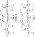
- FIG. 1 shows a generic active bandpass filter (BPF) having input and output buffers 102, resonator couplings 104, and a resonator 106.
- the BPF of FIG. 1 can be made into a tunable BPF if the properties of the resonator can be adjusted. If they can be adjusted using passive elements, then the BPF is a tunable BPF.
- the energy storage of the resonator can also be arranged with feedback in which signal from the output coupling is fed back into the input coupling. This is shown in FIG. 2 , which depicts a generic BPF with a feedback path 110.
- a gain block 112 and delay block 114 may be added that condition the feedback to modify the resonance slightly.
- the addition of a gain block will turn a passive tunable BPF into an active tunable BPF. With this active feedback, more control is possible in which the phase and the amplitude of the feedback can be controlled to give a narrower bandwidth and finer control over the center frequency.
- the resonator feedback can be implemented in which the gain and the delay of the resonator feedback is assumed to be adjustable which modifies the frequency selectivity characteristics of the BPF.
- FIG. 3 shows control of the BPF feedback being implemented with the delay block 114, where the adjustability of the circuit elements is denoted by a diagonal arrow through the element.
- the overall loop gain (the loop consisting of the feedback path 110, couplers 104 and resonator 106) exceeds unity then the BPF becomes an oscillator, resonating at a frequency determined by the properties of the resonator 106 itself and the feedback loop 110. Backing off the feedback gain such that the loop gain is slightly less than unity results in a BPF with an arbitrarily narrow bandwidth. If the resonator 106 selectivity is reduced such that it has a broader pass band then the feedback can tune the filter over a broader range without becoming an oscillator.
- FIG. 4 Another general implementation is shown in FIG. 4 wherein the feedback delay element is replaced by a phase shifter 116, the phase shifter implementing control of the feedback.
- Signal time delay and signal phase shift are approximately analogous for narrow bandpass filters.
- the circuit topology of FIG. 4 is essentially that of the super-regenerative amplifier filter that was developed back in the 1930's (Armstrong). If the resonator 106 is based on a single inductor then the feedback results in a Q-enhanced inductor circuit. If a capacitor is placed in parallel with the Q-enhanced inductor then a tunable filter circuit results. Such circuits are published and well known.
- GB2478585A (Chandler, Stephen Anthony Gerard), published 14 September 2011 , discloses an RF amplifier linearised by RF feedback.
- the centre frequency Q of a resonator in the loop filter is adjusted by a control loop so that the resonator centre frequency follows the frequency of the input RF signal.
- the Q of the resonator which is enhanced by local positive feedback, is similarly optimised by a control loop.
- US 2013/0065542 A1 discloses a spectral transform system including a first path having a signal input, a signal output, and an adjustable first path signal scaling block.
- a second path is connected to the forward path between the signal input and the signal output.
- the second path has an adjustable delay element and an adjustable second path signal scaling block.
- a detector is connected to the signal output for detecting properties of an output signal.
- a controller is connected to adjust the delay element, the second path signal scaling block, and the first path signal scaling block based on the properties detected by the detector to achieve a desired output signal.
- controllable analog filter in accordance with the appended independent apparatus claim as well as a method of filtering an analog electromagnetic signal in accordance with the appended independent method claim.
- the presently described bandpass filter uses a resonator element of variable frequency that may be adjusted such that the resonator center frequency is coincident with the desired center frequency of the tunable filter with feedback. In this way the resonator bandwidth can be narrow enough to avoid spurious passband responses but still be able to tune over a broad range in frequency.
- the gain element which may also be described herein as a scaling block, is adjustable to provide positive gain, negative gain, or zero gain. As will be described in more detail below, this allows the scaling block to act selectively as a Q-enhancer and a Q-spoiler.
- This filter architecture is referred to herein as a controllable analog filter (CAF).
- FIG. 5 A block diagram of the simplest form of the CAF with a variable resonator 502 and a variable scaling block 504 in a signal loop is given in FIG. 5 .
- the description below relates primarily to the design and control aspects of the CAF.
- the CAF is intended to be used in the transmitting, receiving, and/or processing of communications signals for various purposes, some of which are described as examples below.
- a communication signal is a modulated signal used to transmit information or data. Typically, this involves an analog carrier frequency that has been encoded with an information signal, using known methods, such as frequency modulation, amplitude modulation, or phase modulation.
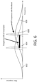
- the fundamental operating principle of the CAF which offers control of bandpass characteristics, is shown in FIG. 6 , where the wide dashed trace 602 is the resonator frequency response at an initial setting.
- the narrow dashed trace 604 is the sharper frequency response of the closed loop filter set for a narrower bandwidth at the initial frequency setting. Assume that the resonator is now tuned upward in frequency to the wide solid trace 606 as indicated by the black arrow.
- the narrow solid trace 608 is the closed loop response that results at the new resonator response frequency.
- the CAF may be of different orders, such as a first, second and third order filter.
- the order of the CAF depends on the filter order of the resonator.
- the CAF may be designed with higher orders beyond the third order, although the complexity of controlling higher order circuits will increase.
- the circuits are, for convenience, typically depicted in the style of FIG. 5 , which shows an arrangement having a main path 508 and a feedback path 510, and generally with the gain block 504 (which may also be referred to as a scaling block and which can have both positive or negative values) on the feedback path 510.
- the gain block 504 which may also be referred to as a scaling block and which can have both positive or negative values
- the circuit may be more appropriately considered as a loop with appropriate input and output couplings, where the loop is formed from what would otherwise be the main path 508 and the feedback path 510, and the elements are connected in series within the loop. As a loop, the order of the components in the loop can be changed without affecting the resonance characteristics of the CAF-n.
- FIG. 7 An example of a circuit with the elements in a different arrangement shown in FIG. 7 , where the gain block 504 is connected in the main path 508, and the variable resonator 502 is connected in the feedback path 510. It will be understood that other variations of the CAF circuit topologies are also possible, and will depend on the number of elements used in the respective circuit.
- CAF-0 a CAF with no resonator
- H ABF 0 s G 1 ⁇ AGe ⁇ j 2 ⁇ P ⁇
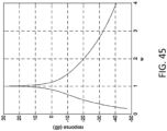
- Such filter performance is commonly referred to as a comb-line filter in reference to the transfer function plotted in FIG. 9 .
- the portion represented by a broken line is the response within the 3 dB bandwidth from which the expression of Q can be validated.
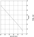
- the excess gain resulting from the feedback path is the power gain normalized by the open loop gain (no feedback path) as G ex ⁇ 20 log Q ⁇ in dB. This is plotted in FIG. 12 .
- the resonator block 1301 is denoted as R in FIG. 13 .
- R is represented by two poles in the S-plane as is also shown in the diagram on the right of FIG. 13 .
- the two poles are represented by 'x'.
- Q control is made possible. This is discussed in detail later.
- resonator block 1401 with feedback incorporating gain or scaling block 802 as shown in FIG. 14 is the basic resonator element that has two control inputs 1302 and 1304: one for changing the frequency (1302), and the other for changing the Q (1304).
- the resonator can be implemented either as a resonator element, such as a LC tank circuit, or as a Second Order Section (SOS) filter element.
- SOS Second Order Section
- the CAF will include a feedback loop comprising a desired number of resonators and a scaling block.
- Each CAF may be connected in parallel or in series with other CAF elements, or other circuit elements, and has an additional level two feedback loop that comprises multiple CAF.
- the term "level two feedback” is intended to refer to a feedback or circuit loop that provides a feedback path around multiple CAF-n elements in series. This may also include what could otherwise be referred to as a level three or level four feedback.
- the resonant frequency of R can be varied with some component included in the resonator circuit. Typically, this may be accomplished using a varactor diode, or a variable dielectric capacitor may be used for a variable capacitance, in which case the 'f control' in FIG. 13 would be an analog bias voltage. Other variants that allow the resonant frequency to be varied may also be used, such as a discrete capacitance that is switched in or out of the circuit and hence 'f control' can be a digital signal. Another variant is that a MEMS variable capacitor or a MEMS variable inductor could be used where 'f control' is a bias control voltage or current signal applied to the MEMS device.
- the variable capacitance or inductance can also be realized by mechanical tuning of a component. For instance, R could be a microwave resonance cavity in which one or more dimensions of the cavity are mechanically adjustable by some mechanism supplying 'f control'.
- the ⁇ Q control' 1304 in FIG. 13 above can comprise a control device associated with the resonator that controls the component Q of the capacitance or the inductance or resonant cavity. If the Q control increases the component Q, this is referred to herein as Q-enhancement. If the Q control decreases the component Q of the resonant cavity, this is referred to herein as Q-spoiling.
- Q-enhancement is equivalent to decreasing D which moves the resonant pole of R closer to the j ⁇ axis of the S-plane. Q-spoiling moves the resonant pole of R further from the j ⁇ axis hence increasing D. It has been found that Q-enhancement and Q-spoiling may be used selectively to move a resonant pole towards or away from the j ⁇ axis to synthesize an arbitrary multi-pole filter function (plurality of R's).
- Scaling blocks 802, as in FIG. 14 are provided in order to enable better control over the feedback response.
- the gain factor for each scaling block 802 is variable and comprises a gain that includes both positive and negative gain values. For example, if the gain of the scaling block 802 is greater than zero, there results Q-enhancement. If the gain of the scaling block 802 is less than zero, there results Q-spoiling.
- each loop or secondary loop in a CAF-n element there will be an additional level two scaling block for each loop or secondary loop in a CAF-n element as discussed below.
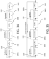
- a CAF-3 circuit element see FIG. 35 for reference
- each scaling block will be capable of enabling Q-enhancement resonators and Q-spoiling resonators independently.
- the resonator may be a Q-enhanced resonator, which uses an amplifier that only allows for Q-enhancement.
- the Q-enhanced resonator would still be nested within the feedback loop of the CAF-n element comprising a scaling block to override the Q-enhancement and provide a desired Q-spoiled performance as required.
- the resonator may be any type of frequency tunable resonator comprising, but not limited to, a varactor diode, a switched discrete capacitor, a variable dielectric capacitor, a variable capacitor, such as a MEMS variable capacitor, a fixed inductor, a variable inductor, such as a MEMS variable inductor, or a mechanically adjustable resonator.
- CAF-1 a first order of the CAF circuit, denoted CAF-1, which comprises a single resonator component 1401, a single gain or scaling block 802, and a combiner 1404 for closing the feedback loop as depicted in FIG. 14 .
- resonator 1401 may be a second order bandpass filter with a transfer function of 1 s 2 + 2 D ⁇ o s + ⁇ o 2 with coefficients evaluated based on D and ⁇ o .
- the gain G 802 is variable and controls the closed loop Q.
- phase shift through the resonator 1401 is ideally 0 degrees.
- the phase shift will not be zero in general due to parasitics and transport effects, but these can be ignored in this evaluation: the implemented circuit will have a phase shifter associated with G 802 that will compensate for any parasitic and transport phase effects.
- the implemented circuit will have a phase shifter associated with G 802 that will compensate for any parasitic and transport phase effects. To vary the frequency it is necessary to change ⁇ o of the resonator in the CAF-1, but this is ignored in this section.
- the first order CAF-1 has a resonator of second order. What is referred to in "order” is the number of Second Order Sections (SOS) used that make up the overall resonator.
- SOS Second Order Sections
- An SOS transfer function refers to a Laplace function of frequency variables that are second order in the denominator.
- H SOS s as s 2 + 2 D ⁇ o s + ⁇ o 2 where ⁇ o is the resonance frequency in radians per second, D is the damping coefficient, and a is a real constant.
- ⁇ f n ,Q ⁇ may then be used interchangeably with ⁇ ⁇ n , D ⁇ .
- the root locus is a standard method of determining the poles of a closed loop system given a variable loop gain.
- the outcome of the root locus calculation in the present context is the trajectory of these closed loop poles as they change with variations in the loop gain G as shown in FIG. 15 for example.
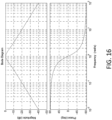
- the Bode plot of the transfer function of the resonator is shown in FIG. 16 . Note that the phase change with frequency is rather gradual around resonance due to the high damping factor (low Q) assumed in this example.
- FIG. 15 the poles of the CAF-1 SOS resonator are represented by an x (1502 or 1504).
- Line 1506 is the closed loop root trajectory as the closed loop gain G is increased from 0 to 1.2. This is the trajectory for the pole indicated by number 1502.
- variable Q for the SOS resonator
- ⁇ Q-spoiler' which is implemented by a variable resistive element in the SOS. This affects the damping coefficient of the SOS which could have been designed to have a higher Q than typically desired.
- the variable resistor reduces (spoils) the Q such that the poles of the SOS are further from the j ⁇ axis into the LHP as mentioned above. This is a degree of freedom (DOF) that allows for higher attenuation of outliers than if an SOS with a fixed lower Q was implemented.
- DOF degree of freedom
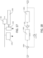
- One embodiment of the Q-spoiler circuit is shown in FIG. 17 based on a parallel resonance SOS 1701.
- the Q-spoiler is implemented with a FET 1702 operating in the triode region in parallel with a resonator 1401 and controlled by a Q-spoiler control voltage 1704 to provide an equivalent variable resistor function.
- the FET 1702 could be implemented with a PIN diode. It will be understood that these design options may be incorporated into any of the variable filter circuits described herein.
- the unit gain buffer 102 separating the resonators is for implementation purposes when necessary to isolate the resonators from each other.
- combiner 1404 provides feedback loop closure.
- the transfer functions of each resonator 1401 are: 1 s 2 + 2 D ⁇ o s + ⁇ o 2
- the zero degree root locus for the CAF-2 is given in FIG. 19 .
- the open loop roots are indicated by 'x', with two poles located at 1902 and two conjugate poles at 1904 as required for this dual SOS resonator configuration.
- the "dominant" pole is always closest to the j ⁇ axis, while the “secondary” pole is furthest from the j ⁇ axis.
- the dominant root trajectories 1906b and 1908b move towards the j ⁇ axis as the closed loop gain G is increased, while the other set of trajectories 1906a and 1908a move away from the j ⁇ axis.
- the two resonator CAF-2 will still have a dominant pole pair that behaves as the single resonator CAF-1.
- the advantage of the two resonator CAF-2 is that the attenuation of out of band signals is larger and therefore the interference signal is less.
- the poles moving along 1906a and 1908a into the left hand plane away from the j ⁇ axis still contribute to attenuation of the out of band spectral components.
- these out of band components flowing around the feedback loop will be less. This is important because the intermodulation distortion performance of the loop components does not have to be as high as in the case of the CAF-1.
- FIG. 21 shows a topology of the CAF-3 which has three cascaded SOS resonators, each of which includes a feedback loop, a method for changing the center frequency of the resonator, and a method for changing the Q of the resonator.
- unit gain buffers 102 are placed between all of the resonators 1401 for isolation, and a combiner 1404 to close the feedback loop. It is important to note the ability to individually control both the center frequency and gain of the individual resonators in this and other CAF-n configurations. Initially, we shall set the center frequency of each resonator to be the same, and will discuss the CAF-3 with different center frequencies later.
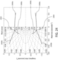
- the Bode plot of the triple resonator, each with the same center frequency, is shown in FIG. 22 where the out of band open loop attenuation of the triple resonator is seen to be 60 dB per decade in frequency which is of significance as it is based on low Q resonators.
- the root locus is interesting in that there are three root trajectories 2306a/b/c and 2308a/b/c emanating from each triple of open loop poles 2302 and 2304 marked again by the 'x', although image scaling makes the three individual roots impossible to differentiate.
- the third pole trajectories 2306c/2308c start to move toward the j ⁇ axis. This potentially gives rise to a spurious mode that is at much lower frequency than the intended passband.
- this potentially troublesome pole is still far from the j ⁇ axis and causes a negligible spurious response in a practical implementation.
- the spurious passband resulting from the 2506d or 2508d paths can be acceptable.
- the CAF-4 root leading to the spurious frequency response is still far from the j ⁇ axis and corresponds to a much lower frequency which can be suppressed with a low pass filter.
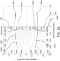
- the root locus in FIG. 26 corresponding to the higher resonator Q, there are two root trajectories 2606d and 2608d that do not really move further into the LHP and consequently create the spurious frequency responses which are generally undesirable in filtering applications.
- the CAF-1 can give good band pass filtering performance for many applications.
- the CAF-2 and CAF-3 filters can give more flexibility for tailoring to an application.
- the CAF-3 will provide the best rejection of the out of band signals for typically encountered closed loop Q values. It is the configurable root trajectory of the second and third order CAF closed loop poles that is a key attribute of this innovation.
- FIG. 27 An application circuit could be as shown in FIG. 27 .
- the single resonator 2702 is a fixed resonator circuit with a feedback gain 2704.
- the gain G of block 2704 can be negative for Q-spoiling or positive for Q-enhancement. It is understood that while gain block 2704 is shown as a two port gain block that it can be arranged as a one port gain block with either negative or positive resistance. Negative resistance would result in G being equivalently greater than zero and provide Q-enhancement. Positive resistance, on the other hand, is equivalent to a negative G providing Q-spoiling.
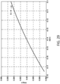
- the root locus of the positive frequency closed loop pole for positive G is shown in FIG. 28 . This corresponds to the Q-enhancement case where the close loop pole moves towards the j ⁇ axis. Likewise the root locus for negative G is shown in FIG. 29 . This corresponds to the Q-spoiling where the close loop pole moves away from the j ⁇ axis.
- the resonator R comprises a means to vary the resonance frequency of the CAF-1.
- the time required to tune from one frequency to the next is approximately equal to the reciprocal of the bandwidth of the CAF-1.
- the operation of the CAF-1, CAF-2, and CAF-3 are compared.
- the Q-enhancement is tuned in the three filters separately such that they have approximately the same close in pass-band response.
- the pass band frequency responses are plotted in FIG. 32 .
- the benefit of the CAF-3 is the higher rejection of the frequency components that are farther from the center frequency as compared to the CAF-2.
- the CAF-2 has better frequency selectivity in comparison to the CAF-1 as expected.
- the equivalent scheme with the three CAP-1s shown where the resonators 1401 each have a feedback path 110 with a scaling block (not shown) and are separated by buffers 102.
- the poles of the three CAF-1s are generated with Q-enhanced inductors that can be set arbitrarily close to the j ⁇ axis.
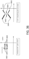
- a level two feedback path 110a may be wrapped around the three CAF-1 modules, such that the circuit will then behave like a CAF-3.
- the arrows 3602 are for negative feedback (Q-spoiling) and the arrows 3604 are for positive feedback (Q-enhancement). Note how the movement is different for the two cases.
- a simpler control is that of having a level two feedback loop 110a as shown in FIG. 35 . In that case, the feedback around each CAF-1 is driven from a common control source (not shown), and each feedback loop has a gain block (not shown), as described herein. Additionally, the outer control loop 110a is around the three individual CAF-1 resonators and also has a gain block (not shown).
- the first control for the CAF-1's moves the three poles in unison towards or away from the j ⁇ axis.
- the CAF-3 level two control can spread the outer flanking poles and cause the center pole to retreat slightly. This enables controlling the bandwidth of the filter while maintaining a similar transition rate.
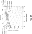
- CAF-1 resonators there will be considered three CAF-1 resonators with the following attributes: Resonator Normalized resonance frequency (f) Damping factor (D) 1 1 .4 2 .95 .42 3 1.05 .38
- each of these three resonators are with feedback loops such that there are 3 cascaded CAF-1 modules.
- the root locus is shown in FIG. 37 .
- the ⁇ x' 3702a/b/c designate the positions of the poles with feedback gain of 0.
- the gain is positive for right excursions 3704a/b/c towards the j ⁇ axis (Q-enhancement) and negative for excursions 3706a/b/c to the left (Q-spoiling).
- Q-enhancement negative resistance amplification
- the range of the feedback gain for each root trajectory is -1 ⁇ G ⁇ 0.9.
- FIG. 40 the left plot is for the negative CAF-3 level two feedback and the right plot is for the positive CAF-3 level two feedback. Note how we can use this to adjust the position of the flanking poles relative to the center pole.
- FIG. 41 shows how the CAF-3 level two feedback can be used to control the bandwidth of the filter. Positive level two feedback narrows the filter bandwidth and negative level two feedback broadens it. Only a very small amount of CAF-3 level two feedback is needed for this control. In FIG. 41 , the level two feedback was 0, -0.002, and +0.002, as indicated.
- the CAF-3 level two feedback control of FIG. 35 allows for an effective means of bandwidth control that can be practically implemented.
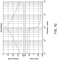
- FIG. 43 shows the zero degree root locus of this configuration, which is very similar to that shown in FIG. 23 where each of the three SOS resonators has the same center frequency.
- the various elements in the CAF-n circuits may be controlled using a controller. It will be understood that various types of controllers may be used as is known in the art, comprising controller circuits and various microprocessors. Furthermore, while there is preferably a single controller that controls the various elements of the CAF-n, there may also be multiple controllers, or various layers of controllers.
- the controllers may be programmed to adjust the variables in the CAF-n according to an algorithm, a lookup table, software, or according to other known strategies, all of which may depend on specific implementation objectives and appropriate tradeoffs for that implementation.
- the controller may be programmed to respond to inputs from a user or from other circuit elements.
- the CAF-n may be controlled by providing the controller with a desired frequency response, which then controls the variables in order to achieve the desired frequency response. This may allow for an iterative approach to be used, or for fine adjustments to be made after the controller has approximated the desired frequency response.
- the control of the CAF-n is relatively simple in that the closed loop center frequency control and the closed loop Q are almost independent and the control optimization is strictly convex. In other words, the control of the closed loop Q and center frequency can be done independently for many adjustments, which simplifies the system control algorithm.
- CAF-n tuning and tracking scheme This is an example of an embodiment of such a scheme, and it is understood that a wide variety of such tuning and tracking algorithms can be implemented by one skilled in the art.
- a simple tuning scheme in which there exists a means of estimating the dominant pole location of the closed loop CAF-n. This may be done, for example, by measuring the impulse response of the CAF-n and determining the resonant frequency of ⁇ o and the damping coefficient D o . Alternately, this can be input as a user design target. Then a tracking loop determines 1) the overall feedback gain G, and 2) the SOS resonator(s) natural frequency denoted by ⁇ r .
- G can be determined by setting a control voltage on the feedback amplifier, and ⁇ r is set by adjusting the voltage on a varactor diode of the SOS resonant tank.
- D d and ⁇ d be the desired damping and resonant frequency respectively provided by the user design targets.
- the tracking loop is straightforward: if D o > D d then G is increased incrementally. If ⁇ o > ⁇ d then ⁇ r is increased incrementally. The loop iterates, updating G and ⁇ r sequentially indefinitely until the desired response is achieved. In this way the initial configuration of the CAF-n is accomplished and also the temperature variations and component aging of the CAF-n are ameliorated. Furthermore, the desired D d and ⁇ d can vary with time and the CAF-n will track these.
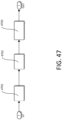
- multiple CAF-n elements each of which may include one or more loop circuits with resonators and gain elements as discussed above, can be configured in series and parallel combinations to realize multi-pole bandpass filters.
- three CAF-1 elements 4701, 4702, and 4703 are shown to be connected in series.
- each CAF-1 4701/4702/4703 has a frequency response of that of a first order bandpass filter (one resonant pole in the positive frequency region) and each CAF-1 is adjusted such that it has the appropriate Q and resonant frequency commensurate with the desired overall filter response.
- the transfer function of CAF-1 4701 is set at: s s 2 + .1 s + 0.96
- the transfer function of CAF-1 4702 is set at: s s 2 + .1 s + 1
- the transfer function of CAF-1 4703 is set at: s s 2 + .1 s + 1.02
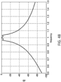
- FIG. 48 A typical response of three CAF-1 elements 4701/4702/4703 in series is shown in FIG. 48 .
- the series connections of CAF-1's are useful for realizing single band bandpass filters.
- a parallel connection of CAF-n's may be used.
- An example of a filter topology providing two separate bands is given in FIG. 49 . This is accomplished by a parallel connection of two CAF-3 filters 4901 and 4902 centered at the respective bands. The general response of such a filter is shown in FIG. 50 .
- level two feedback of FIG. 35 is an example of level two feedback that could be applied.
- bandpass filters discussed above are examples with practical utility. It will be understood that other series and parallel combinations of CAF-n's can be used to realize bandpass filters designed to achieve a desired frequency response.
- CAF-1 5101 is: s s 2 + .1 s + 1.4
- the transfer function of CAF-1 5102 is: s s 2 + .1 s + 1.45
- the transfer function of CAF-1 5103 is: s s 2 + .1 s + 0.96
- the transfer function of CAF-1 5104 is: s s 2 + .1 s + 1
- the transfer function of CAF-1 5105 is: s s 2 + .1 s + 1.02
- the transfer function of CAF-1 5106 is: s s 2 + .1 s + 2
- the frequency response may also be changed by adding level two feedback paths to form signal loops.
- circuits may be designed that allow for a desired frequency response, and that may be controlled as desired.
- one embodiment may be a larger programmable chip in which a number of generic CAF-n's are built with a switch matrix analogous to ALU's in an FPGA device. This is illustrated in FIG. 52 .
- a plurality of input and output buffers 102 are attached to a switch matrix 5202, which also can connect the input and output of CAF-n 5204 components.
- an arbitrary order bandpass filter can be created by cascading such components as shown in FIG. 53 , which is an example of a third order band pass filter, with the various components connected to provide a desired signal path 5302.
- FIG. 52 and FIG. 53 are examples of what may be possible using a switch matrix 5202, although other configurations are possible.
- the switch matrix may have additional CAF-n elements or other circuit elements that can be connected in parallel, in series, or in combinations thereof. In this way, a fabric of CAF-n filters may be customized for specific applications.
- poles and zeros are first grouped into complex conjugate pairs. While the combining or grouping of a pair of conjugate poles and pair of conjugate zeros is somewhat arbitrary, there are generally implementation issues that favor some groupings over others. Generally poles and zeros are grouped that are closer together in a Euclidean sense in the S-plane.
- An example of a 4 th order Butterworth bandpass filter with a passband between the normalized frequencies of 1 and 1.5 is considered, decomposed into four SOS sections.
- a desirable feature of the Butterworth filter is that it has an optimally flat passband.
- FIG. 54 shows the frequency response of the Butterworth emphasizing this passband flatness.
- the left side response curve FIG. 54a is magnified on the right side FIG. 54b to provide detail in the passband down to -3 dB.
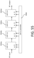
- SOS sections 5502a/b/c/d are placed in series as shown in FIG. 55 and controlled by a controller 5504.
- the series connection of the SOS CAF-1 elements 5502a/b/c/d is preferred as this avoids having to use parallel connections that have to be scaled and phased to a precise value.
- the CAF-4 configuration of FIG. 55 will be used.
- each of the four CAF-1 elements are of modest Q, notwithstanding the gain flatness and the steep transition of the fourth order Butterworth.
- the frequency response of the cascaded set of four CAF-1's, represented by line 5604 is also shown in FIG. 56 , presenting a reasonable match to the desired Butterworth response, represented by line 5606, with which we started.
- the out of band transition of the four CAF-1's implementation of this example is actually steeper than that of the original Butterworth filter. This is because of the extra poles in the CAF-1's. However, the shoulders are softer than desired. This may be corrected with a better optimization.
- FIG. 57 A parallel type implementation of a second order SOS filter element 5702 is shown in FIG. 57 .
- the Q-spoiler 5708 moves the resonant pole horizontally along the real axis and the variable capacitor control 5710 moves the pole vertically along the imaginary axis.
- FIG. 58 shows a parallel resonance circuit 5802 with a variable resistor 5808 controlled by control input 5804, and a variable capacitor 5810 controlled control input 5806 by the Q-spoiler.
- the three SOS CAF-1resonators may be combined into a single 3 rd order bandpass filter topology consisting of two series resonators 5902 and one parallel resonator 5904.
- the depiction of resonators 5902 and 5904 has been simplified and does not include the various control elements, etc. discussed above.
- This circuit offers a smaller implementation footprint as the inter-SOS buffers are not required.
- a disadvantage is that it is harder to tune.
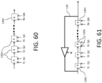
- the first level of generalization is that a number of R resonators 1301 can be cascaded as shown in FIG. 60 .
- N such resonators 1301 are cascaded with controls of ⁇ f1,Q1 ⁇ to ⁇ fN,QN ⁇ .
- Level two feedback is implemented across selected adjacent individual resonator elements for improved performance as described herein.
- a feedback path 110 with variable gain G is then around the N cascaded resonators 1301 to form a signal loop as shown in FIG. 61 .
- the feedback gain is in general complex and referred to as vector modulation. This implies that the magnitude of G can be varied from zero to some maximum value.
- the phase can be varied over 2 ⁇ radians.
- FIG. 62 shows the symbol used to represent a generalized CAF-n 6202 with the control inputs as ⁇ G1,f1,Q1,...,GN,fN,QN ⁇ .
- the next layer of generalization is that several CAF-n's 6202 can be cascaded with a feedback loop 110a with gain as shown in FIG. 63 .
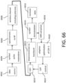
- a block diagram of the transceiver is as shown in FIG. 64 .
- a T/R switch block 6402 connects the receiver 6404 and the transmitter 6406 to the antenna 6408.
- the CAF-3 6410 can provide the spectral shaping of the transmitted signal generated by the transmitter processing block 6406.
- the CAF-3 6412 filters out interfering signals and centers a passband on the desired receive signal for the receiver processing block 6404.
- CAF-3 is frequency agile (that is, the frequency can quickly be tuned from one passband to another) there is an option of having only a single CAF-3 6502 that is shared by the transmitter and receiver functions 6406 and 6404. In the example shown, this is achieved by a circuit that uses a T/R switch 6504 with two ports and a power detector 6506.
- An enhanced implementation of the telemetric transceiver for sensor applications is the cognitive radio aspect of the CAF-3 in which a broad segment of the spectrum is continuously scanned to monitor activity. The idea is to find a spectral region in which there is little activity. Finding such a spectral hole, the transceiver can begin data communications operations using minimal transmit power and maximal Signal to Noise ratio (SNR) consistent with the environment.
- SNR Signal to Noise ratio
- Finding such a spectral hole is achieved by setting up the CAF-3 for a Q-enhanced narrow band filter response that is swept over the potential frequency band by varying the f controls of the three Rs in the CAF-3.
- a simple power detector at the output of the CAF-3 can be used to estimate the spectral power at the frequency of the CAF-3.
- the detector output is then a function of the applied frequency control for the R's. After completing a sweep the desirable spectral region(s) can be determined.
- CAF-3 To integrate the CAF-3 into the transceiver we have to have a means of providing a control feedback for stabilizing the approximate position of the closed loop poles. This can be done within the forward open loop control by setting the control voltages based on the desired spectral location using a reference CAF cell on the same die. The impulse response of this reference die would be measured based on a quartz crystal based time reference that then accounts for variables such as temperature, aging, chip supply voltage, and so forth. An adaptive feedback is used to precisely tune the CAF-3. This adaptive control can be implemented without additional circuitry based on using the measured outputs of the innate baseband processing already part of the data communications receiver.
- An input data source 6602 is baseband modulated with a symbol or pulse shaping function 6604. This is then up-converted to RF by block 6606 and transmitted over the wireless channel 6608.
- the wireless channel 6608 will include standard thermal noise as well as interference from wireless sources in adjacent channels.
- the signal is intercepted by the receiver antenna (not shown) then filtered in a CAF-3 6610, down converted in block 6612 and then a baseband filter 6614 is applied that matches the pulse shaping filter of the transmitter. Then the data is extracted as block 6616.
- the SNR of the demodulation process is available which is used in the block ⁇ adaptive optimization of CAF-3' 6618, which has an algorithm 6620 for optimizing the control settings of a CAF-3 6610.
- the output of this block is converted to voltage control signals in block 6622 for the actual CAF-3 as shown.
- the objective of the optimizer is to maximize the SNR of the data demodulation process.
- the SNR is sensitive to the pole placement of the CAF-3, it gives us a means of continuously adapting the control of the CAF-3.
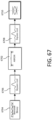
- FIG. 67 depicts an ideal AWGN (added white Gaussian noise) channel 6702, which is connected to a Bernoulli binary generator block 6704, a raised cosine transmit filter block 6706, a raised cosine receive filter block 6708, and a discrete-time eye diagram scope 6710.
- AWGN added white Gaussian noise
- the matched filter is optimum in terms of achieving the maximum eye SNR.
- a root raised cosine (RRC) pulse shaping is used for the transmitted signal in block 6706 and also for the received signal in block 6708.
- RRC root raised cosine
- the CAF-3 merely deteriorates the eye unless it is of bandwidth wider than the signal.
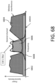
- the channel also has noise from interference from adjacent channels. This is illustrated in FIG.
- the AWGN is indicated by 6802
- the power spectral density (PSD) of the interference signal is indicated by 6804.
- the desired communication channel is indicated by 6806
- the optimum response of the CAF-3 filter is indicated by 6808.
- RRC filter which is shown in FIG. 69a and 69b . It is an FIR representation of the RRC filter that has 8 samples per symbol epoch and is 10 symbols long. The frequency response of the filter is given on the right with respect to half the sampling rate (fundamental sampling rate is 8 times per symbol).
- the power spectral density (PSD) of the total noise is given in FIG. 70 . Note that the dB scale is relative.
- the filter above is modeled by setting the bandwidth at 0.44 Hz relative to an 8 Hz normalized sampling rate.
- FIG. 71 we have the pole/zero pattern for a CAF-3 filter with a normalized bandwidth of .08 Hz with 8 Hz sampling.
- the center frequency offset of the CAF-3 can be represented by a complex discrete time filter by simply rotating the pole zero pattern in FIG. 71 by an amount commensurate with the frequency offset.
- the CAF-3 feedback for the optimization merely uses the maximum SNR as determined to adjust the filter controls. It is necessary to use a dithering control to do this that varies the three CAF-3 controls:
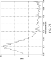
- FIG. 73 shows the plot of the SNR which has a clear maximum inferring to a normalized bandwith of 0.1 relative to the symbol rate is optimum. Note that the distortion caused by the CAF-3 which leads to eye closure is offset by the reduction of noise resulting from the large interference on either side of the signal passband.
- the examples above demonstrate the ability of using the feedback from the communications receiver demodulator output into the optimizer that adjusts the CAF-3 feedback as well as the three CAF-1s.
- modulation and demodulation schemes There are of course many different modulation and demodulation schemes as there are many ways of gathering metrics for the optimization of the CAF control.
- the SNR of the sampling as shown in this document, is simple and available without further hardware required to the receiver.
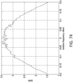
- the general CAF-n will have multiple controls. These can be set in a ⁇ feed forward' manner as will be described in the next section. However, this assumes that the optimum operating point of the CAF-n is known and a LUT (look up table) maps the desired operating point to physical voltages of ⁇ f,Q,G ⁇ . In the sensor communications tracking problem example given in the previous section the optimum operating point is not known and varies depending on the current interference conditions. The goal in this example is to optimize the SNR of the receiver output. From FIG. 73 and 74 , there is clearly at least a local optimum that depends on the two parameters of G and f.
- Q was set first for the Rs and then the tracking loop would set G and f.
- the SNR of the communications receiver output for a specific instance of interference in the power spectral domain be denoted as g ( G , f ) . It is understood that g ( G,f ) will change with time as the spectral interference is unknown and uncontrollable.
- ⁇ G new ⁇ G present + ⁇ ⁇ g ⁇ G present
- ⁇ f and ⁇ G depend on the application. This is a form of dithering control which can be applied to an optimizer when the objective function is essentially unknown. If the interference changes slowly then ⁇ f and ⁇ G can be small, however, this requires a longer dwell time to measure the commensurate small change in SNR. If the interference changes more rapidly then it is necessary to use a larger dithering step size of the parameters to be optimized. Generally dithering schemes are robust and simple to implement but seldom provide the best performance as it does not take advantage of known characteristics of the objective function.
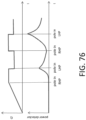
- FIG. 75 is based on a circuit that has processing built in for the purpose of calibrating and stabilizing the response of a CAF-1 block 7502.
- the microprocessor 7504 through a DAC implemented as a PWM (pulse width modulation) circuit 7506 and based on readings from a temperature sensor 7508, adjusts the control for the frequency and Q of the CAF-1 7502. It drives this such that the CAF-1 7502 just starts to self-oscillate.
- the frequency of this self-oscillation is down converted in block 7510 by a frequency synthesizer signal generated by a crystal reference 7505 and a frequency synthesizer 7507 that is set also by the microprocessor 7504.
- a frequency counter 7509 or other measurement means determines the frequency of the down-converted signal. In this way the resonant frequency of the CAF-1 can be determined.
- a power detector 7512 and ADC block 7514 that can estimate the rate of increase of the self-oscillation signal at the output of the CAF-1 7502.
- the microprocessor 7504 estimates this exponential rise of power and from this determines where the closed loop pole of the CAF-1 7502 is. Presently it will be just to the right of the jw axis. If the Q-enhancement is decreased slightly then the self-oscillation will continue at the same frequency to a high accuracy but will begin to decay exponentially. No the pole is on the left hand side of the jw axis. Again based on the power detector 7512, this exponential decay can be measured and the operating point measured.
- the mapping of the CAF-1 7502 to the f and Q control signals can be completed.
- This calibration can be done based on circuitry on chip that requires no additional off chip components except for the crystal reference source. During operation calibration breaks can be made such that the LUT 7516 is continuously updated. In the case of the wireless sensor, the transmitter and receiver functions are separated by epochs of inactivity in which the calibration processing can be done.
- FIG. 76 shows an example of the Q control of the CAF-1 alternated between higher and lower levels that alternately places the closed loop pole of the CAF-1 in the right hand and left hand planes.
- the resulting exponential rise and decay is easily measured by the power detector with numerical analysis done on the microprocessor.
- the applied Q control voltage can be mapped to a specific pole position. This is stored in the LUT such that when a pole position is required for the filtering operations of the CAF-1 then the LUT can be interpolated and the ⁇ f, Q ⁇ control voltages set.
- the real part of the closed pole value is easily measured.
- the pole is in the right hand plane such that it has the form of a exp ( bt ) where a and b are constants that are unknown.
- Either the times of t 1 and t 2 can be set and the voltages x 1 and x 2 measured or else fixed thresholds can be set at x 1 and x 2 and the time difference of t 2 - t 1 measured. Either approach is straight forward.
- the CAF-n can be designed to be relatively easy to broaden the bandwidth.
- a small amount of feedback gain G around the 3 Rs of a CAF-3 is simple and robust way to change the passband from something representing a single pole passband response to a broader response similar to a second order Chebyshev.
- the CAF-3 can be configured on the fly to be a sensor for power spectral density for a cognitive radio, then provide a transmitter filter for this passband and a receiver filter using T/R switches to reorient the filter for transmit and receive functions.
- the receive mode we can tie the CAF-3 into an adaptive loop that uses the SNR of the digital sampled output to optimize filter parameters. As the ⁇ f,Q ⁇ control is orthogonal this SNR optimization is robustly achieved with a simple dithering algorithm. Finally in setting up the CAF-3 it is necessary to know where the poles are located as a function of the controls. This can be achieved by using a CAF-1 on chip for calibration purposes.
- the envelope of the self-oscillation of the CAF-1 can be used as a probe signal to estimate the real part of the pole location.
- the imaginary component is determined by the frequency of self-oscillation.
- the self-oscillation can be measured based on comparison with a crystal locked synthesizer frequency.
- the Rs of the CAF-3 can also be used directly.
- implementing the CAF-1 allows for calibration to be continuous and in parallel with the operation of the CAF-3 which is then dedicated for the actual signal processing.
- the measurements of the CAF-1 pole location as a function of the control voltages and perhaps chip temperature is stored in a LUT. The values of the LUT are interpolated when the CAF-3 is to be configured.
- CAF may include, but are not limited to: Equalizer for an antenna to provide a flat antenna response (enhanced filtenna); Optimized front end module (FEM); Frequency synthesizer; Integrated sensor/cognitive radio system for remote patient monitoring; Low cost sensor transceiver network for Smart roads, Smart signs, and Smart/Driverless cars; Enhanced WiFi systems operating at both 2.4 GHz and 5.0 GHz; Enhanced Bluetooth systems; General high performance analog tunable RF filtering; Spectrum surveillance systems for electronic warfare applications; Automobile proximity radar modules operating at very high frequency (above 20 GHz) for collision avoidance; Variable and tunable delay-line modules; Phase control modules; Enhanced sensitivity detectors for remote sensing applications; Drone surveillance and control;
- phase shifter As is known in the art, the phase of a signal may be affected by many different factors as it passes through a circuit, some of which include stray component capacitances and inductances that may be referred to as "parasitics". As a result, it may be necessary to incorporate a phase shifter to correct the phase of a signal passing through the circuit.
- the phase shifter used will depend on the actual implementation of the circuit.
- Various types of phase shifters are known in the art, and a person of ordinary skill may incorporate a suitable phase shifter into a CAF-n as needed.
- a fixed phase shifter may be adequate for a CAF-n circuit that is implemented on a chip, where parasitics are generally minimal, well modeled and understood, and where the CAF-n circuit is intended to be used over a modest frequency range. In other circumstances, it may be necessary to incorporate a variable phase shifter.
- the closed loop passband of the CAF-1 forms around the range of frequency where the open loop phase shift is a multiple of 360 degrees.
- the passband of the resonator may be arranged to coincide with the frequency of a multiple of 360 degrees phase shift. If the resonator peak frequency is misaligned, then the closed loop response peak will still coincide with the frequency at which a multiple of 360 is achieved, although the passband may be distorted.
- a detuned resonator adds a phase shift and can be used to add a controllable modest phase shift.
- Any phase shifter is really an implementation of a variable delay with some associated magnitude response that is frequency dependent.
- a variable phase shift may be introduced by starting with a variable delay line that is made up of a uniform sequence of varactor diodes along a transmission line.
- the group delay can be varied, and by changing the group delay, the phase can be shifted.
- variable phase shifters, resonators, delay lines and quadrature modulators may be considered as circuits arranged and optimized to provide a variable delay over a range of frequencies.
- variable resonator and variable phase shifter By generalizing the variable resonator and variable phase shifter and recognizing that they are functionally similar in the context of application to the CAF-n, it is possible to use a plurality of sub-circuits in the loop, where each sub-circuit can be controlled to give a desired delay and amplitude response that can be controlled by a plurality of control voltages.
- FIG. 77 shows a variable delay line with a ladder network of inductors 7702 and capacitors 7704, where the capacitors 7704 are variable, and may be varactor diodes. Port matching of this sub-circuit gives rise to a magnitude response which may be optimized for a desired frequency range.
- a series or parallel resonator may be used, which include an inductor 7702, a variable capacitor 7704, and resistors 7706 as required.
- FIG. 78 shows a possible tunable delay line having inductors 7702 and capacitors 7704.
- the capacitors 7704 are controllable with a tuning voltage, as represented by the arrows.
- FIG. 79 shows a possible phase shifter having a parallel resonance circuit with resistors 7706, a variable capacitor 7704, and an inductor 7702, where the capacitor 7704 is variable by an applied tuning voltage as represented by the arrow.
- FIG. 80 shows a possible implementation of a phase shifter implemented using a hybrid coupler 8002, which may be described as a distributed or lumped element hybrid coupler, or rat race coupler, where variable capacitors 7704 are attached to the coupled ports.
- the phase of coupler 8002 is controllable by appropriate adjustments of the capacitors 7704.
- the phase shift may be a multiple of 360 degrees at a desired frequency within the passband of the resonator. Shifting the resonant frequency equivalently shifts the phase.
- the CAF-1 response peak will occur where the loop phase shift is a multiple of 360 degrees.
- the limitation with the CAF-1 with only a variable resonator is that the phase shift adjustment of the resonator is limited. Hence if the loop has a large phase error, then there is not enough range with the single resonator, requiring a variable and fixed phase shifter to be added. However, based on the above discussion, this is equivalent to stringing a number of delay controllable sub-circuits in series.
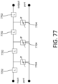
- variable phase shifter has a flatter frequency response in terms of magnitude and can therefore be used over a larger frequency range, but this comes at a cost of adding more components, some of which are difficult to integrate into a chip. If three resonators are added, this is equivalent to a CAF-3. This is shown in FIG. 81 , with three variable resonators 502, which may be CAF-1 elements, a feedback path 110, a coupler 104, and a gain element 112, which may be controllable.
Claims (11)
- Filtre analogique contrôlable, comprenant :une boucle de signal secondaire comprenant un chemin principal secondaire et un chemin de rétroaction secondaire (110a) connecté entre une entrée de signal et une sortie de signal, la boucle de signal secondaire comprenant une pluralité de boucles de signal primaires dans le chemin principal secondaire et un bloc de mise à l'échelle ajustable secondaire dans le chemin de rétroaction secondaire ;chacune de la pluralité de boucles de signaux primaires comprend un chemin principal primaire (508), un chemin de rétroaction primaire (110, 510) et plusieurs éléments de circuit connectés en série dans chacune de la pluralité de boucles de signaux primaires, la pluralité d'éléments de circuit comprenant :un résonateur accordable en fréquence (502, 1401) connecté soit au chemin principal primaire, soit au chemin de rétroaction primaire (110) ; etun bloc de mise à l'échelle réglable primaire (504, 802, 2704) connecté soit dans le chemin de rétroaction primaire (110) soit dans le chemin principal primaire, respectivement, et configuré pour appliquer un facteur de gain, le facteur de gain étant réglable dans une plage qui comprend un gain positif et un gain négatif ; etun contrôleur connecté pour accorder chaque résonateur accordable en fréquence et pour ajuster le facteur de gain de chacun des blocs d'échelle ajustables primaires et du bloc d'échelle ajustable secondaire entre un facteur de gain négatif et un facteur de gain positif vers une réponse en fréquence désirée du filtre analogique contrôlable.
- Filtre analogique contrôlable selon la revendication 1, dans lequel le contrôleur (1302, 1304) contrôle un déphasage dans la boucle du signal en ajustant une fréquence d'au moins un résonateur accordable en fréquence de la pluralité de résonateurs accordables en fréquence (1401).
- Filtre analogique contrôlable selon la revendication 1, dans lequel deux ou plusieurs résonateurs accordables en fréquence (1401) sont connectés en série dans le chemin principal primaire de chaque boucle de signal primaire de la pluralité de boucles de signal primaire, chacune des boucles de signal primaire étant connectée en série dans la boucle du signal secondaire.
- Filtre analogique contrôlable selon la revendication 1, dans lequel le contrôleur (1302, 1304) est programmé pour étouffer ou améliorer sélectivement un ou plusieurs résonateurs accordables en fréquence (1401) vers la réponse en fréquence souhaitée en contrôlant un bloc d'échelle primaire réglable correspondant pour appliquer le facteur de gain négatif ou positif, respectivement.
- Circuit de filtrage analogique à plusieurs étages, comprenant :
une pluralité d'éléments filtrants (1301), dans lequel la pluralité d'éléments filtrants (1301) est choisie dans un groupe constitué d'un filtre variable tel que défini dans l'une des revendications 1 à 4, et dans lequel deux éléments filtrants ou plus sont en parallèle ou en série. - Procédé de filtrage d'un signal électromagnétique analogique, le procédé comprenant les étapes consistant à :
fournir un filtre analogique contrôlable comprenant :une boucle de signal secondaire comprenant un chemin principal secondaire et un chemin de rétroaction secondaire (110a) connecté entre une entrée de signal et une sortie de signal, la boucle de signal secondaire comprenant une pluralité de boucles de signal primaires dans le chemin principal secondaire et un bloc de mise à l'échelle ajustable secondaire dans le chemin de rétroaction secondaire ;chacune de la pluralité de boucles de signaux primaires comprenant un chemin principal primaire, un chemin de rétroaction primaire (110, 510) et une pluralité d'éléments de circuit connectés en série dans la boucle de signaux primaires respective, la pluralité d'éléments de circuit comprenant :un résonateur accordable en fréquence (502, 1401) connecté soit à le chemin principal primaire, soit à le chemin de rétroaction primaire (110) ; etun bloc de mise à l'échelle réglable primaire (504, 802, 2704) connecté soit au chemin de rétroaction primaire (110) soit au chemin principal primaire, respectivement, et configuré pour appliquer un facteur de gain, le facteur de gain étant réglable dans une plage qui comprend un gain positif et un gain négatif ; et accorder chaque résonateur accordable en fréquence et régler le facteur de gain de chacun des blocs de mise à l'échelle primaires réglables et du bloc de mise à l'échelle secondaire réglable entre un facteur de gain négatif et un facteur de gain positif vers une réponse en fréquence souhaitée du filtre analogique contrôlable. - Procédé selon la revendication 6, comprenant en outre l'étape de contrôle d'un déphasage dans la boucle de signal (110) en réglant les résonateurs accordables en fréquence (1401).
- Procédé selon la revendication 7, dans lequel le contrôle du déphasage consiste à désaccorder les résonateurs accordables en fréquence (1401) à partir d'une fréquence centrale du filtre analogique contrôlable
- Procédé selon la revendication 6, dans lequel deux ou plusieurs résonateurs accordables en fréquence (1401) sont connectés en série dans le chemin principal primaire de chaque boucle de signal primaire de la pluralité de boucles de signal primaire, chacune des boucles de signal primaire étant connectée en série dans la boucle de signal secondaire.
- Procédé selon la revendication 6, dans lequel les résonateurs accordables en fréquence (1401) sont sélectivement étouffés ou améliorés vers la réponse en fréquence désirée, en contrôlant un bloc de mise à l'échelle primaire réglable correspondant pour appliquer le facteur de gain négatif ou positif, respectivement.
- Procédé selon la revendication 6, comprenant en outre une étape d'étalonnage dans laquelle les valeurs de contrôle dans une table de recherche sont déterminées sur la base d'une stabilité d'une réponse en fréquence du filtre analogique contrôlable lors de l'ajustement d'au moins le facteur de gain des blocs d'échelle ajustables primaires (802) et du bloc d'échelle ajustable secondaire (802).
Priority Applications (1)
| Application Number | Priority Date | Filing Date | Title |
|---|---|---|---|
| EP23182890.6A EP4243284A3 (fr) | 2015-11-23 | 2016-11-23 | Filtre variable |
Applications Claiming Priority (2)
| Application Number | Priority Date | Filing Date | Title |
|---|---|---|---|
| US201562258867P | 2015-11-23 | 2015-11-23 | |
| PCT/GB2016/053686 WO2017089803A1 (fr) | 2015-11-23 | 2016-11-23 | Filtre variable |
Related Child Applications (1)
| Application Number | Title | Priority Date | Filing Date |
|---|---|---|---|
| EP23182890.6A Division EP4243284A3 (fr) | 2015-11-23 | 2016-11-23 | Filtre variable |
Publications (2)
| Publication Number | Publication Date |
|---|---|
| EP3381126A1 EP3381126A1 (fr) | 2018-10-03 |
| EP3381126B1 true EP3381126B1 (fr) | 2023-07-05 |
Family
ID=57442741
Family Applications (2)
| Application Number | Title | Priority Date | Filing Date |
|---|---|---|---|
| EP16804863.5A Active EP3381126B1 (fr) | 2015-11-23 | 2016-11-23 | Filtre variable |
| EP23182890.6A Pending EP4243284A3 (fr) | 2015-11-23 | 2016-11-23 | Filtre variable |
Family Applications After (1)
| Application Number | Title | Priority Date | Filing Date |
|---|---|---|---|
| EP23182890.6A Pending EP4243284A3 (fr) | 2015-11-23 | 2016-11-23 | Filtre variable |
Country Status (10)
| Country | Link |
|---|---|
| US (2) | US10050604B2 (fr) |
| EP (2) | EP3381126B1 (fr) |
| JP (1) | JP6770083B2 (fr) |
| KR (1) | KR20180087341A (fr) |
| CN (1) | CN109314505B (fr) |
| IL (1) | IL259540B2 (fr) |
| MY (1) | MY192162A (fr) |
| RU (2) | RU2018122759A (fr) |
| SG (2) | SG11201804302XA (fr) |
| WO (1) | WO2017089803A1 (fr) |
Families Citing this family (31)
| Publication number | Priority date | Publication date | Assignee | Title |
|---|---|---|---|---|
| MY192162A (en) | 2015-11-23 | 2022-08-03 | Anlotek Ltd | Variable filter |
| US9900197B1 (en) | 2016-10-03 | 2018-02-20 | Keyssa Systems, Inc. | BPSK demodulation |
| CN111034041B (zh) * | 2017-05-24 | 2023-10-31 | 安乐泰克有限公司 | 用于控制谐振器的装置和方法 |
| US10498212B2 (en) * | 2017-05-26 | 2019-12-03 | Dialog Semiconductor (Uk) Limited | Gate driver |
| US10355674B2 (en) * | 2017-07-24 | 2019-07-16 | Arm Limited | Clock gating circuit |
| US10783223B2 (en) * | 2017-10-12 | 2020-09-22 | Pacesetter, Inc. | Hybrid signal processing circuit for implantable medical devices and methods |
| US10164618B1 (en) * | 2017-12-28 | 2018-12-25 | Micron Technology, Inc. | Jitter cancellation with automatic performance adjustment |
| GB201801241D0 (en) * | 2018-01-25 | 2018-03-14 | Eosemi Ltd | Temperature compensated oscillator |
| CN109905095B (zh) * | 2019-03-28 | 2021-06-04 | 电子科技大学 | 低频段的窄带可调滤波器 |
| CN110401431B (zh) * | 2019-07-18 | 2020-11-10 | 江苏康众数字医疗科技股份有限公司 | 一种频率跟随数字离散滤波器、实现方法及其应用 |
| US11277110B2 (en) | 2019-09-03 | 2022-03-15 | Anlotek Limited | Fast frequency switching in a resonant high-Q analog filter |
| EP4070171A1 (fr) | 2019-12-05 | 2022-10-12 | Anlotek Limited | Utilisation de filtres analogiques à rétroaction active accordables stables dans la synthèse de fréquence |
| EP3890189A1 (fr) * | 2020-03-30 | 2021-10-06 | Anlotek Limited | Filtres analogiques de rétroaction active avec résonateurs couplés |
| CN111585929B (zh) * | 2020-05-13 | 2020-12-15 | 安徽省安泰科技股份有限公司 | 基于云计算的5g移动网络监控系统 |
| US11876499B2 (en) | 2020-06-15 | 2024-01-16 | Anlotek Limited | Tunable bandpass filter with high stability and orthogonal tuning |
| US11381230B2 (en) * | 2020-09-04 | 2022-07-05 | Northeastern University | Microelectromechanical tunable delay line circuit |
| US20230361719A1 (en) * | 2020-09-14 | 2023-11-09 | Anlotek Limited | Oscillator with a multiple pole resonator |
| RU2748610C1 (ru) * | 2020-12-08 | 2021-05-28 | федеральное государственное бюджетное образовательное учреждение высшего образования «Донской государственный технический университет» (ДГТУ) | Широкополосный полосовой фильтр четвертого порядка с одним входом и парафазным выходом |
| RU2749605C1 (ru) * | 2020-12-08 | 2021-06-16 | федеральное государственное бюджетное образовательное учреждение высшего образования «Донской государственный технический университет» (ДГТУ) | Широкополосный полосовой фильтр четвертого порядка |
| RU2760871C1 (ru) * | 2021-02-09 | 2021-12-01 | федеральное государственное бюджетное образовательное учреждение высшего образования «Донской государственный технический университет» (ДГТУ) | Полосовой фильтр четвертого порядка |
| RU2752254C1 (ru) * | 2021-02-09 | 2021-07-23 | федеральное государственное бюджетное образовательное учреждение высшего образования «Донской государственный технический университет» (ДГТУ) | Полосовой фильтр четвертого порядка |
| TWI778525B (zh) * | 2021-02-24 | 2022-09-21 | 中原大學 | 前饋式主動噪音控制系統的設計方法 |
| TWI740783B (zh) * | 2021-02-24 | 2021-09-21 | 中原大學 | 具類比濾波器之前饋式主動噪音控制系統的設計方法 |
| EP4054076A1 (fr) | 2021-02-27 | 2022-09-07 | Anlotek Limited | Filtre multi-pôle actif |
| EP4084333A1 (fr) | 2021-04-30 | 2022-11-02 | Anlotek Limited | Réduction du bruit de phase dans un résonateur rf analogique variable à condensateurs à valeur fixe et commutables |
| EP4089920A1 (fr) | 2021-05-12 | 2022-11-16 | Anlotek Limited | Commutation de fréquence rapide dans un filtre rf variable |
| US11817630B2 (en) | 2021-09-17 | 2023-11-14 | City University Of Hong Kong | Substrate integrated waveguide-fed Fabry-Perot cavity filtering wideband millimeter wave antenna |
| WO2023056533A1 (fr) * | 2021-10-10 | 2023-04-13 | Shaun Joseph Cunningham | Dispositif et procédé de déploiement et de commande de prises actives |
| CN113890561B (zh) * | 2021-11-17 | 2023-07-21 | 歌尔科技有限公司 | 一种电子设备及其射频电路 |
| CN114265314B (zh) * | 2021-12-23 | 2022-06-24 | 哈尔滨工业大学 | 一种基于fir滤波的鲁棒逆模型学习增益设计方法 |
| CN117176100B (zh) * | 2023-11-03 | 2024-02-23 | 苏州博海创业微系统有限公司 | 一种改善带内平坦度的带通滤波电路及滤波器 |
Citations (2)
| Publication number | Priority date | Publication date | Assignee | Title |
|---|---|---|---|---|
| EP1675263A1 (fr) * | 2004-12-23 | 2006-06-28 | Lucent Technologies Inc. | Réglage du facteur qualité (Q) d'un filtre |
| WO2011103108A1 (fr) * | 2010-02-16 | 2011-08-25 | Sky Holdings Company, Llc | Systèmes de filtrage spectral |
Family Cites Families (63)
| Publication number | Priority date | Publication date | Assignee | Title |
|---|---|---|---|---|
| WO1990013175A1 (fr) | 1989-04-21 | 1990-11-01 | N.V. Philips' Gloeilampenfabrieken | Amplificateur a circuits accordes |
| US5311198A (en) | 1990-08-23 | 1994-05-10 | The United States Of America As Represented By The Administrator Of The National Aeronautics And Space Administration | Active antenna |
| US5291159A (en) | 1992-07-20 | 1994-03-01 | Westinghouse Electric Corp. | Acoustic resonator filter with electrically variable center frequency and bandwidth |
| US5491604A (en) | 1992-12-11 | 1996-02-13 | The Regents Of The University Of California | Q-controlled microresonators and tunable electronic filters using such resonators |
| US5550520A (en) * | 1995-04-11 | 1996-08-27 | Trw Inc. | Monolithic HBT active tuneable band-pass filter |
| US5854593A (en) | 1996-07-26 | 1998-12-29 | Prince Corporation | Fast scan trainable transmitter |
| US5917387A (en) | 1996-09-27 | 1999-06-29 | Lucent Technologies Inc. | Filter having tunable center frequency and/or tunable bandwidth |
| US6253092B1 (en) * | 1997-11-25 | 2001-06-26 | Uniden Financial, Inc. | Closed loop transmitter with DAC sensitivity adjusted to detector nonlinearity |
| CA2224261A1 (fr) | 1997-12-09 | 1999-06-09 | Philsar Electronics Inc. | Amplificateur a faible bruit de phase, a facteur q eleve et a gain eleve dans un circuit integre |
| US6347237B1 (en) | 1999-03-16 | 2002-02-12 | Superconductor Technologies, Inc. | High temperature superconductor tunable filter |
| US6356143B2 (en) | 1999-11-01 | 2002-03-12 | Intreon Corporation | Method and apparatus for filtering radio frequency signals |
| ATE313873T1 (de) | 2000-05-16 | 2006-01-15 | Stephen Anthony Gerar Chandler | Rückgekoppelte hochfrequenzverstärker |
| US6452465B1 (en) | 2000-06-27 | 2002-09-17 | M-Squared Filters, Llc | High quality-factor tunable resonator |
| US7174147B2 (en) | 2001-04-11 | 2007-02-06 | Kyocera Wireless Corp. | Bandpass filter with tunable resonator |
| EP1251635A1 (fr) | 2001-04-20 | 2002-10-23 | Semiconductor Ideas to The Market (ItoM) BV | Amplificateur à résonance accordable |
| JP3880329B2 (ja) | 2001-04-20 | 2007-02-14 | 株式会社日立国際電気 | ループゲイン制御方法及び電力増幅回路 |
| US6771147B2 (en) | 2001-12-17 | 2004-08-03 | Remec, Inc. | 1-100 GHz microstrip filter |
| US6954774B1 (en) | 2001-12-20 | 2005-10-11 | Rockwell Collins | Bandpass filter with ability to tune a pass frequency, passband gain and filter Q |
| DE10325396A1 (de) | 2003-05-28 | 2004-12-23 | Atmel Germany Gmbh | Schaltungsanordnung und Verfahren zur Phasenmodulation für rückstreubasierte Transponder |
| GB2403086B (en) | 2003-06-17 | 2005-07-20 | Motorola Inc | Cartesian loop transmitter and method of adjusting an output level of such transmitter |
| FR2864727B1 (fr) | 2003-12-29 | 2007-05-11 | St Microelectronics Sa | Circuit electronique comportant un resonateur destine a etre integre dans un produit semi-conducteur |
| DE102004028068A1 (de) * | 2004-06-09 | 2005-12-29 | Epcos Ag | Oszillator |
| US7522016B2 (en) | 2004-09-15 | 2009-04-21 | Qualcomm, Incorporated | Tunable surface acoustic wave resonators |
| US7433668B2 (en) | 2004-12-23 | 2008-10-07 | Lucent Technologies Inc. | Controlling Q-factor of filters |
| EP2838167A1 (fr) | 2005-01-20 | 2015-02-18 | Massachusetts Institute of Technology | Procédés et appareil de verrouillage de mode |
| JP4922677B2 (ja) | 2005-07-01 | 2012-04-25 | パナソニック株式会社 | 無線通信装置 |
| US7400203B2 (en) | 2006-08-03 | 2008-07-15 | Broadcom Corporation | Circuit with Q-enhancement cell having feedback loop |
| KR100921383B1 (ko) | 2006-09-08 | 2009-10-14 | 가부시키가이샤 엔.티.티.도코모 | 가변 공진기, 대역폭 가변 필터, 전기회로 장치 |
| US7639101B2 (en) | 2006-11-17 | 2009-12-29 | Superconductor Technologies, Inc. | Low-loss tunable radio frequency filter |
| TWI326156B (en) * | 2007-01-04 | 2010-06-11 | Mstar Semiconductor Inc | Method for tuning tunable filter |
| JP4724135B2 (ja) | 2007-02-22 | 2011-07-13 | 株式会社エヌ・ティ・ティ・ドコモ | 可変共振器、可変フィルタ、電気回路装置 |
| RU2340079C1 (ru) * | 2007-02-26 | 2008-11-27 | Федеральное государственное унитарное предприятие Омский научно-исследовательский институт приборостроения | Активный полосовой пьезоэлектрический фильтр |
| JP2008301182A (ja) * | 2007-05-31 | 2008-12-11 | Fujitsu Microelectronics Ltd | フィルタ回路および半導体装置 |
| CN101755396B (zh) | 2007-06-29 | 2014-02-19 | 汤姆森特许公司 | 用于传输射频信号的转发器 |
| GB2453099A (en) * | 2007-07-19 | 2009-04-01 | Univ Sussex | Sensor system with tunable narrow band filter. |
| FR2920927B1 (fr) | 2007-09-11 | 2011-05-06 | Commissariat Energie Atomique | Procede d'adaptation automatique d'impedance de circuit radiofrequence et chaine d'emission ou reception a adaptation automatique |
| US7917117B2 (en) | 2008-01-28 | 2011-03-29 | University Of Washington | Auto-tuning amplifier |
| US7884680B2 (en) | 2008-06-30 | 2011-02-08 | Infineon Technologies Ag | Dynamically adjustable Q-factors |
| WO2010040119A1 (fr) | 2008-10-03 | 2010-04-08 | Purdue Research Foundation | Filtre à cavité réglable à mode évanescent |
| US7994870B2 (en) | 2008-10-20 | 2011-08-09 | Qualcomm, Incorporated | Tunable filter with gain control circuit |
| FR2939581B1 (fr) * | 2008-12-09 | 2010-11-26 | Commissariat Energie Atomique | Reseau de resonateurs couples, filtre passe-bande et oscillateur. |
| US8166084B2 (en) * | 2009-03-27 | 2012-04-24 | Intersil Americas Inc. | Calibration of adjustable filters |
| US8362853B2 (en) | 2009-06-19 | 2013-01-29 | Qualcomm Incorporated | Tunable MEMS resonators |
| US8538367B2 (en) * | 2009-06-29 | 2013-09-17 | Qualcomm Incorporated | Buffer circuit with integrated loss canceling |
| US9166564B2 (en) | 2010-02-04 | 2015-10-20 | Hittite Microwave Corporation | Wideband analog bandpass filter |
| US8724731B2 (en) | 2010-02-26 | 2014-05-13 | Intersil Americas Inc. | Methods and systems for noise and interference cancellation |
| GB2478585A (en) * | 2010-03-11 | 2011-09-14 | Stephen Anthony Gerard Chandler | An RF amplifier linearised by RF feedback, and having a loop filter resonator of enhanced Q |
| US8427243B2 (en) * | 2011-02-17 | 2013-04-23 | Mediatek Inc. | Signal generating circuit and signal generating method |
| CN102098018A (zh) | 2011-03-10 | 2011-06-15 | 江苏苏美达机电有限公司 | 一种可调带通滤波器系统 |
| US8767871B2 (en) | 2011-06-08 | 2014-07-01 | Broadcom Corporation | Antenna tuning using the ratio of complex forward and reflected signals |
| US9407239B2 (en) | 2011-07-06 | 2016-08-02 | Hrl Laboratories, Llc | Wide bandwidth automatic tuning circuit |
| GB2494652A (en) | 2011-09-14 | 2013-03-20 | Stephen Anthony Gerard Chandler | A transmitter amplifier with linearising RF feedback and automatic control of resonator Q, resonator frequency, loop phase, and loop gain |
| US9236846B2 (en) | 2011-12-06 | 2016-01-12 | Futurewei Technologies, Inc. | Tunable bandpass filter device and method |
| CN103248336B (zh) * | 2012-02-09 | 2016-04-06 | 联发科技股份有限公司 | 滤波器 |
| US8941441B2 (en) | 2013-03-15 | 2015-01-27 | Innophase Inc. | LNA with linearized gain over extended dynamic range |
| US8766712B2 (en) | 2012-05-04 | 2014-07-01 | Analog Devices, Inc. | Quality factor tuning for LC circuits |
| US9774311B2 (en) * | 2013-03-15 | 2017-09-26 | Qorvo Us, Inc. | Filtering characteristic adjustments of weakly coupled tunable RF filters |
| CN203574616U (zh) * | 2013-11-22 | 2014-04-30 | 宁波杉工结构监测与控制工程中心有限公司 | 一种截止频率和增益可调的多通道低通滤波器 |
| WO2015176041A1 (fr) | 2014-05-15 | 2015-11-19 | The Regents Of The University Of California | Système résonateur actif avec facteur de qualité, fréquence et impédance accordables |
| US9813033B2 (en) | 2014-09-05 | 2017-11-07 | Innophase Inc. | System and method for inductor isolation |
| US9735752B2 (en) | 2014-12-03 | 2017-08-15 | Tdk Corporation | Apparatus and methods for tunable filters |
| CN104538714B (zh) | 2014-12-25 | 2017-04-26 | 深圳顺络电子股份有限公司 | 一种中心频率可调的带通滤波器 |
| MY192162A (en) | 2015-11-23 | 2022-08-03 | Anlotek Ltd | Variable filter |
-
2016
- 2016-11-23 MY MYPI2018701945A patent/MY192162A/en unknown
- 2016-11-23 RU RU2018122759A patent/RU2018122759A/ru not_active Application Discontinuation
- 2016-11-23 RU RU2020121155A patent/RU2738030C2/ru active
- 2016-11-23 EP EP16804863.5A patent/EP3381126B1/fr active Active
- 2016-11-23 US US15/360,813 patent/US10050604B2/en active Active
- 2016-11-23 CN CN201680075929.8A patent/CN109314505B/zh active Active
- 2016-11-23 SG SG11201804302XA patent/SG11201804302XA/en unknown
- 2016-11-23 JP JP2018545704A patent/JP6770083B2/ja active Active
- 2016-11-23 WO PCT/GB2016/053686 patent/WO2017089803A1/fr active Application Filing
- 2016-11-23 IL IL259540A patent/IL259540B2/en unknown
- 2016-11-23 KR KR1020187017924A patent/KR20180087341A/ko not_active Application Discontinuation
- 2016-11-23 SG SG10202004720SA patent/SG10202004720SA/en unknown
- 2016-11-23 EP EP23182890.6A patent/EP4243284A3/fr active Pending
-
2018
- 2018-07-10 US US16/031,911 patent/US10879875B2/en active Active
Patent Citations (2)
| Publication number | Priority date | Publication date | Assignee | Title |
|---|---|---|---|---|
| EP1675263A1 (fr) * | 2004-12-23 | 2006-06-28 | Lucent Technologies Inc. | Réglage du facteur qualité (Q) d'un filtre |
| WO2011103108A1 (fr) * | 2010-02-16 | 2011-08-25 | Sky Holdings Company, Llc | Systèmes de filtrage spectral |
Non-Patent Citations (1)
| Title |
|---|
| ANONYMOUS: "Roll-off", 30 September 2015 (2015-09-30), https://en.wikipedia.org/w/index.php?title=Roll-off&oldid=683494320, pages 1 - 4, XP055934710, Retrieved from the Internet <URL:https://en.wikipedia.org/w/index.php?title=Roll-off&oldid=683494320> [retrieved on 20220623] * |
Also Published As
| Publication number | Publication date |
|---|---|
| EP4243284A3 (fr) | 2023-10-11 |
| MY192162A (en) | 2022-08-03 |
| US10050604B2 (en) | 2018-08-14 |
| CN109314505A (zh) | 2019-02-05 |
| EP4243284A2 (fr) | 2023-09-13 |
| RU2020121155A3 (fr) | 2020-10-14 |
| IL259540B1 (en) | 2023-10-01 |
| JP6770083B2 (ja) | 2020-10-14 |
| IL259540A (en) | 2018-07-31 |
| IL259540B2 (en) | 2024-02-01 |
| CN109314505B (zh) | 2022-08-05 |
| EP3381126A1 (fr) | 2018-10-03 |
| US20180323770A1 (en) | 2018-11-08 |
| SG10202004720SA (en) | 2020-06-29 |
| WO2017089803A1 (fr) | 2017-06-01 |
| JP2018536368A (ja) | 2018-12-06 |
| SG11201804302XA (en) | 2018-06-28 |
| RU2018122759A (ru) | 2019-12-26 |
| RU2018122759A3 (fr) | 2020-04-28 |
| KR20180087341A (ko) | 2018-08-01 |
| US20170149411A1 (en) | 2017-05-25 |
| US10879875B2 (en) | 2020-12-29 |
| RU2738030C2 (ru) | 2020-12-07 |
| RU2020121155A (ru) | 2020-07-08 |
Similar Documents
| Publication | Publication Date | Title |
|---|---|---|
| EP3381126B1 (fr) | Filtre variable | |
| US10027310B2 (en) | Low-loss tunable radio frequency filter | |
| KR101563373B1 (ko) | 신호 제거 기능을 이용한 필터 정형 | |
| US7212789B2 (en) | Tunable duplexer | |
| US9160045B2 (en) | Reconfigurable bandpass filter based on a planar combline filter comprising varactor diodes | |
| US11804362B2 (en) | Frequency tuning for modulated plasma systems | |
| EP3039802B1 (fr) | Procédé d'accord simplifié d'antenne en boucle fermée | |
| US20130009720A1 (en) | Wide bandwidth automatic tuning circuit | |
| US20200350140A1 (en) | Apparatus and system for modulated plasma systems | |
| KR20140072827A (ko) | 기판의 유전율 분산이 보상된 무선 주파수 디바이스 및 조정 방법 | |
| Koohi et al. | Intrinsically switchable filter bank employing ferroelectric barium strontium titanate | |
| CN108063605B (zh) | 射频滤波器与调谐射频滤波器的方法 | |
| CN109196712B (zh) | 磁感应波导 | |
| TWI721048B (zh) | 可變類比濾波器、多極點濾波器、以及濾波類比電磁信號之方法 | |
| EP3890189A1 (fr) | Filtres analogiques de rétroaction active avec résonateurs couplés | |
| US20230261628A1 (en) | A tunable resonator | |
| Lakhan | ELECTRONICS and COMMUNICATION ENGINEERING |
Legal Events
| Date | Code | Title | Description |
|---|---|---|---|
| STAA | Information on the status of an ep patent application or granted ep patent |
Free format text: STATUS: UNKNOWN |
|
| STAA | Information on the status of an ep patent application or granted ep patent |
Free format text: STATUS: THE INTERNATIONAL PUBLICATION HAS BEEN MADE |
|
| PUAI | Public reference made under article 153(3) epc to a published international application that has entered the european phase |
Free format text: ORIGINAL CODE: 0009012 |
|
| STAA | Information on the status of an ep patent application or granted ep patent |
Free format text: STATUS: REQUEST FOR EXAMINATION WAS MADE |
|
| 17P | Request for examination filed |
Effective date: 20180618 |
|
| AK | Designated contracting states |
Kind code of ref document: A1 Designated state(s): AL AT BE BG CH CY CZ DE DK EE ES FI FR GB GR HR HU IE IS IT LI LT LU LV MC MK MT NL NO PL PT RO RS SE SI SK SM TR |
|
| AX | Request for extension of the european patent |
Extension state: BA ME |
|
| DAV | Request for validation of the european patent (deleted) | ||
| DAX | Request for extension of the european patent (deleted) | ||
| STAA | Information on the status of an ep patent application or granted ep patent |
Free format text: STATUS: EXAMINATION IS IN PROGRESS |
|
| 17Q | First examination report despatched |
Effective date: 20210223 |
|
| STAA | Information on the status of an ep patent application or granted ep patent |
Free format text: STATUS: EXAMINATION IS IN PROGRESS |
|
| GRAP | Despatch of communication of intention to grant a patent |
Free format text: ORIGINAL CODE: EPIDOSNIGR1 |
|
| STAA | Information on the status of an ep patent application or granted ep patent |
Free format text: STATUS: GRANT OF PATENT IS INTENDED |
|
| INTG | Intention to grant announced |
Effective date: 20220919 |
|
| GRAJ | Information related to disapproval of communication of intention to grant by the applicant or resumption of examination proceedings by the epo deleted |
Free format text: ORIGINAL CODE: EPIDOSDIGR1 |
|
| STAA | Information on the status of an ep patent application or granted ep patent |
Free format text: STATUS: EXAMINATION IS IN PROGRESS |
|
| INTC | Intention to grant announced (deleted) | ||
| GRAP | Despatch of communication of intention to grant a patent |
Free format text: ORIGINAL CODE: EPIDOSNIGR1 |
|
| STAA | Information on the status of an ep patent application or granted ep patent |
Free format text: STATUS: GRANT OF PATENT IS INTENDED |
|
| INTG | Intention to grant announced |
Effective date: 20230116 |
|
| GRAS | Grant fee paid |
Free format text: ORIGINAL CODE: EPIDOSNIGR3 |
|
| GRAA | (expected) grant |
Free format text: ORIGINAL CODE: 0009210 |
|
| STAA | Information on the status of an ep patent application or granted ep patent |
Free format text: STATUS: THE PATENT HAS BEEN GRANTED |
|
| P01 | Opt-out of the competence of the unified patent court (upc) registered |
Effective date: 20230424 |
|
| P02 | Opt-out of the competence of the unified patent court (upc) changed |
Effective date: 20230427 |
|
| AK | Designated contracting states |
Kind code of ref document: B1 Designated state(s): AL AT BE BG CH CY CZ DE DK EE ES FI FR GB GR HR HU IE IS IT LI LT LU LV MC MK MT NL NO PL PT RO RS SE SI SK SM TR |
|
| REG | Reference to a national code |
Ref country code: CH Ref legal event code: EP |
|
| REG | Reference to a national code |
Ref country code: AT Ref legal event code: REF Ref document number: 1585750 Country of ref document: AT Kind code of ref document: T Effective date: 20230715 |
|
| REG | Reference to a national code |
Ref country code: DE Ref legal event code: R096 Ref document number: 602016080838 Country of ref document: DE |
|
| REG | Reference to a national code |
Ref country code: IE Ref legal event code: FG4D |
|
| REG | Reference to a national code |
Ref country code: LT Ref legal event code: MG9D |
|
| REG | Reference to a national code |
Ref country code: NL Ref legal event code: MP Effective date: 20230705 |
|
| REG | Reference to a national code |
Ref country code: AT Ref legal event code: MK05 Ref document number: 1585750 Country of ref document: AT Kind code of ref document: T Effective date: 20230705 |
|
| PG25 | Lapsed in a contracting state [announced via postgrant information from national office to epo] |
Ref country code: NL Free format text: LAPSE BECAUSE OF FAILURE TO SUBMIT A TRANSLATION OF THE DESCRIPTION OR TO PAY THE FEE WITHIN THE PRESCRIBED TIME-LIMIT Effective date: 20230705 |
|
| PG25 | Lapsed in a contracting state [announced via postgrant information from national office to epo] |
Ref country code: GR Free format text: LAPSE BECAUSE OF FAILURE TO SUBMIT A TRANSLATION OF THE DESCRIPTION OR TO PAY THE FEE WITHIN THE PRESCRIBED TIME-LIMIT Effective date: 20231006 |
|
| PGFP | Annual fee paid to national office [announced via postgrant information from national office to epo] |
Ref country code: GB Payment date: 20231114 Year of fee payment: 8 |
|
| PG25 | Lapsed in a contracting state [announced via postgrant information from national office to epo] |
Ref country code: ES Free format text: LAPSE BECAUSE OF FAILURE TO SUBMIT A TRANSLATION OF THE DESCRIPTION OR TO PAY THE FEE WITHIN THE PRESCRIBED TIME-LIMIT Effective date: 20230705 |
|
| PG25 | Lapsed in a contracting state [announced via postgrant information from national office to epo] |
Ref country code: IS Free format text: LAPSE BECAUSE OF FAILURE TO SUBMIT A TRANSLATION OF THE DESCRIPTION OR TO PAY THE FEE WITHIN THE PRESCRIBED TIME-LIMIT Effective date: 20231105 |
|
| PG25 | Lapsed in a contracting state [announced via postgrant information from national office to epo] |
Ref country code: SE Free format text: LAPSE BECAUSE OF FAILURE TO SUBMIT A TRANSLATION OF THE DESCRIPTION OR TO PAY THE FEE WITHIN THE PRESCRIBED TIME-LIMIT Effective date: 20230705 Ref country code: RS Free format text: LAPSE BECAUSE OF FAILURE TO SUBMIT A TRANSLATION OF THE DESCRIPTION OR TO PAY THE FEE WITHIN THE PRESCRIBED TIME-LIMIT Effective date: 20230705 Ref country code: PT Free format text: LAPSE BECAUSE OF FAILURE TO SUBMIT A TRANSLATION OF THE DESCRIPTION OR TO PAY THE FEE WITHIN THE PRESCRIBED TIME-LIMIT Effective date: 20231106 Ref country code: NO Free format text: LAPSE BECAUSE OF FAILURE TO SUBMIT A TRANSLATION OF THE DESCRIPTION OR TO PAY THE FEE WITHIN THE PRESCRIBED TIME-LIMIT Effective date: 20231005 Ref country code: LV Free format text: LAPSE BECAUSE OF FAILURE TO SUBMIT A TRANSLATION OF THE DESCRIPTION OR TO PAY THE FEE WITHIN THE PRESCRIBED TIME-LIMIT Effective date: 20230705 Ref country code: LT Free format text: LAPSE BECAUSE OF FAILURE TO SUBMIT A TRANSLATION OF THE DESCRIPTION OR TO PAY THE FEE WITHIN THE PRESCRIBED TIME-LIMIT Effective date: 20230705 Ref country code: IS Free format text: LAPSE BECAUSE OF FAILURE TO SUBMIT A TRANSLATION OF THE DESCRIPTION OR TO PAY THE FEE WITHIN THE PRESCRIBED TIME-LIMIT Effective date: 20231105 Ref country code: HR Free format text: LAPSE BECAUSE OF FAILURE TO SUBMIT A TRANSLATION OF THE DESCRIPTION OR TO PAY THE FEE WITHIN THE PRESCRIBED TIME-LIMIT Effective date: 20230705 Ref country code: GR Free format text: LAPSE BECAUSE OF FAILURE TO SUBMIT A TRANSLATION OF THE DESCRIPTION OR TO PAY THE FEE WITHIN THE PRESCRIBED TIME-LIMIT Effective date: 20231006 Ref country code: FI Free format text: LAPSE BECAUSE OF FAILURE TO SUBMIT A TRANSLATION OF THE DESCRIPTION OR TO PAY THE FEE WITHIN THE PRESCRIBED TIME-LIMIT Effective date: 20230705 Ref country code: ES Free format text: LAPSE BECAUSE OF FAILURE TO SUBMIT A TRANSLATION OF THE DESCRIPTION OR TO PAY THE FEE WITHIN THE PRESCRIBED TIME-LIMIT Effective date: 20230705 Ref country code: AT Free format text: LAPSE BECAUSE OF FAILURE TO SUBMIT A TRANSLATION OF THE DESCRIPTION OR TO PAY THE FEE WITHIN THE PRESCRIBED TIME-LIMIT Effective date: 20230705 |
|
| PGFP | Annual fee paid to national office [announced via postgrant information from national office to epo] |
Ref country code: FR Payment date: 20231129 Year of fee payment: 8 Ref country code: DE Payment date: 20231115 Year of fee payment: 8 |
|
| PG25 | Lapsed in a contracting state [announced via postgrant information from national office to epo] |
Ref country code: PL Free format text: LAPSE BECAUSE OF FAILURE TO SUBMIT A TRANSLATION OF THE DESCRIPTION OR TO PAY THE FEE WITHIN THE PRESCRIBED TIME-LIMIT Effective date: 20230705 |
|
| PG25 | Lapsed in a contracting state [announced via postgrant information from national office to epo] |
Ref country code: SM Free format text: LAPSE BECAUSE OF FAILURE TO SUBMIT A TRANSLATION OF THE DESCRIPTION OR TO PAY THE FEE WITHIN THE PRESCRIBED TIME-LIMIT Effective date: 20230705 Ref country code: RO Free format text: LAPSE BECAUSE OF FAILURE TO SUBMIT A TRANSLATION OF THE DESCRIPTION OR TO PAY THE FEE WITHIN THE PRESCRIBED TIME-LIMIT Effective date: 20230705 Ref country code: EE Free format text: LAPSE BECAUSE OF FAILURE TO SUBMIT A TRANSLATION OF THE DESCRIPTION OR TO PAY THE FEE WITHIN THE PRESCRIBED TIME-LIMIT Effective date: 20230705 Ref country code: DK Free format text: LAPSE BECAUSE OF FAILURE TO SUBMIT A TRANSLATION OF THE DESCRIPTION OR TO PAY THE FEE WITHIN THE PRESCRIBED TIME-LIMIT Effective date: 20230705 Ref country code: CZ Free format text: LAPSE BECAUSE OF FAILURE TO SUBMIT A TRANSLATION OF THE DESCRIPTION OR TO PAY THE FEE WITHIN THE PRESCRIBED TIME-LIMIT Effective date: 20230705 Ref country code: SK Free format text: LAPSE BECAUSE OF FAILURE TO SUBMIT A TRANSLATION OF THE DESCRIPTION OR TO PAY THE FEE WITHIN THE PRESCRIBED TIME-LIMIT Effective date: 20230705 |