EP2964418B1 - System and method for high power diode based additive manufacturing - Google Patents
System and method for high power diode based additive manufacturing Download PDFInfo
- Publication number
- EP2964418B1 EP2964418B1 EP14760359.1A EP14760359A EP2964418B1 EP 2964418 B1 EP2964418 B1 EP 2964418B1 EP 14760359 A EP14760359 A EP 14760359A EP 2964418 B1 EP2964418 B1 EP 2964418B1
- Authority
- EP
- European Patent Office
- Prior art keywords
- optical signal
- substrate
- mask
- liquid crystal
- layer
- Prior art date
- Legal status (The legal status is an assumption and is not a legal conclusion. Google has not performed a legal analysis and makes no representation as to the accuracy of the status listed.)
- Active
Links
- 238000004519 manufacturing process Methods 0.000 title claims description 32
- 238000000034 method Methods 0.000 title claims description 31
- 239000000654 additive Substances 0.000 title claims description 12
- 230000000996 additive effect Effects 0.000 title claims description 12
- 230000003287 optical effect Effects 0.000 claims description 40
- 239000000758 substrate Substances 0.000 claims description 38
- 239000000463 material Substances 0.000 claims description 22
- 239000004973 liquid crystal related substance Substances 0.000 claims description 16
- 239000012254 powdered material Substances 0.000 claims description 13
- 230000010287 polarization Effects 0.000 claims description 6
- 230000001678 irradiating effect Effects 0.000 claims description 3
- 239000007921 spray Substances 0.000 claims 1
- 239000000843 powder Substances 0.000 description 20
- 229910052751 metal Inorganic materials 0.000 description 8
- 239000002184 metal Substances 0.000 description 8
- 230000008901 benefit Effects 0.000 description 7
- 238000003491 array Methods 0.000 description 4
- 238000000151 deposition Methods 0.000 description 3
- 230000004907 flux Effects 0.000 description 3
- 150000002739 metals Chemical class 0.000 description 3
- XEEYBQQBJWHFJM-UHFFFAOYSA-N Iron Chemical compound [Fe] XEEYBQQBJWHFJM-UHFFFAOYSA-N 0.000 description 2
- 230000008021 deposition Effects 0.000 description 2
- 238000003754 machining Methods 0.000 description 2
- 229910001175 oxide dispersion-strengthened alloy Inorganic materials 0.000 description 2
- 238000010146 3D printing Methods 0.000 description 1
- 229910000831 Steel Inorganic materials 0.000 description 1
- RTAQQCXQSZGOHL-UHFFFAOYSA-N Titanium Chemical compound [Ti] RTAQQCXQSZGOHL-UHFFFAOYSA-N 0.000 description 1
- 229910045601 alloy Inorganic materials 0.000 description 1
- 239000000956 alloy Substances 0.000 description 1
- 229910052782 aluminium Inorganic materials 0.000 description 1
- XAGFODPZIPBFFR-UHFFFAOYSA-N aluminium Chemical compound [Al] XAGFODPZIPBFFR-UHFFFAOYSA-N 0.000 description 1
- 210000000988 bone and bone Anatomy 0.000 description 1
- 239000003795 chemical substances by application Substances 0.000 description 1
- 238000005286 illumination Methods 0.000 description 1
- 238000003384 imaging method Methods 0.000 description 1
- 239000007943 implant Substances 0.000 description 1
- 229910052742 iron Inorganic materials 0.000 description 1
- 238000002844 melting Methods 0.000 description 1
- 230000008018 melting Effects 0.000 description 1
- 238000012986 modification Methods 0.000 description 1
- 230000004048 modification Effects 0.000 description 1
- 239000004033 plastic Substances 0.000 description 1
- 229920003023 plastic Polymers 0.000 description 1
- 230000005855 radiation Effects 0.000 description 1
- 238000007493 shaping process Methods 0.000 description 1
- 238000005245 sintering Methods 0.000 description 1
- 239000007787 solid Substances 0.000 description 1
- 230000000087 stabilizing effect Effects 0.000 description 1
- 239000010959 steel Substances 0.000 description 1
- 239000010936 titanium Substances 0.000 description 1
- 229910052719 titanium Inorganic materials 0.000 description 1
- WFKWXMTUELFFGS-UHFFFAOYSA-N tungsten Chemical compound [W] WFKWXMTUELFFGS-UHFFFAOYSA-N 0.000 description 1
- 229910052721 tungsten Inorganic materials 0.000 description 1
- 239000010937 tungsten Substances 0.000 description 1
Images


Classifications
-
- B—PERFORMING OPERATIONS; TRANSPORTING
- B29—WORKING OF PLASTICS; WORKING OF SUBSTANCES IN A PLASTIC STATE IN GENERAL
- B29C—SHAPING OR JOINING OF PLASTICS; SHAPING OF MATERIAL IN A PLASTIC STATE, NOT OTHERWISE PROVIDED FOR; AFTER-TREATMENT OF THE SHAPED PRODUCTS, e.g. REPAIRING
- B29C64/00—Additive manufacturing, i.e. manufacturing of three-dimensional [3D] objects by additive deposition, additive agglomeration or additive layering, e.g. by 3D printing, stereolithography or selective laser sintering
- B29C64/10—Processes of additive manufacturing
- B29C64/141—Processes of additive manufacturing using only solid materials
- B29C64/153—Processes of additive manufacturing using only solid materials using layers of powder being selectively joined, e.g. by selective laser sintering or melting
-
- B—PERFORMING OPERATIONS; TRANSPORTING
- B22—CASTING; POWDER METALLURGY
- B22F—WORKING METALLIC POWDER; MANUFACTURE OF ARTICLES FROM METALLIC POWDER; MAKING METALLIC POWDER; APPARATUS OR DEVICES SPECIALLY ADAPTED FOR METALLIC POWDER
- B22F10/00—Additive manufacturing of workpieces or articles from metallic powder
- B22F10/20—Direct sintering or melting
- B22F10/28—Powder bed fusion, e.g. selective laser melting [SLM] or electron beam melting [EBM]
-
- B—PERFORMING OPERATIONS; TRANSPORTING
- B22—CASTING; POWDER METALLURGY
- B22F—WORKING METALLIC POWDER; MANUFACTURE OF ARTICLES FROM METALLIC POWDER; MAKING METALLIC POWDER; APPARATUS OR DEVICES SPECIALLY ADAPTED FOR METALLIC POWDER
- B22F10/00—Additive manufacturing of workpieces or articles from metallic powder
- B22F10/30—Process control
- B22F10/36—Process control of energy beam parameters
- B22F10/366—Scanning parameters, e.g. hatch distance or scanning strategy
-
- B—PERFORMING OPERATIONS; TRANSPORTING
- B22—CASTING; POWDER METALLURGY
- B22F—WORKING METALLIC POWDER; MANUFACTURE OF ARTICLES FROM METALLIC POWDER; MAKING METALLIC POWDER; APPARATUS OR DEVICES SPECIALLY ADAPTED FOR METALLIC POWDER
- B22F12/00—Apparatus or devices specially adapted for additive manufacturing; Auxiliary means for additive manufacturing; Combinations of additive manufacturing apparatus or devices with other processing apparatus or devices
- B22F12/40—Radiation means
- B22F12/41—Radiation means characterised by the type, e.g. laser or electron beam
- B22F12/43—Radiation means characterised by the type, e.g. laser or electron beam pulsed; frequency modulated
-
- B—PERFORMING OPERATIONS; TRANSPORTING
- B22—CASTING; POWDER METALLURGY
- B22F—WORKING METALLIC POWDER; MANUFACTURE OF ARTICLES FROM METALLIC POWDER; MAKING METALLIC POWDER; APPARATUS OR DEVICES SPECIALLY ADAPTED FOR METALLIC POWDER
- B22F12/00—Apparatus or devices specially adapted for additive manufacturing; Auxiliary means for additive manufacturing; Combinations of additive manufacturing apparatus or devices with other processing apparatus or devices
- B22F12/40—Radiation means
- B22F12/44—Radiation means characterised by the configuration of the radiation means
-
- B—PERFORMING OPERATIONS; TRANSPORTING
- B23—MACHINE TOOLS; METAL-WORKING NOT OTHERWISE PROVIDED FOR
- B23K—SOLDERING OR UNSOLDERING; WELDING; CLADDING OR PLATING BY SOLDERING OR WELDING; CUTTING BY APPLYING HEAT LOCALLY, e.g. FLAME CUTTING; WORKING BY LASER BEAM
- B23K26/00—Working by laser beam, e.g. welding, cutting or boring
- B23K26/02—Positioning or observing the workpiece, e.g. with respect to the point of impact; Aligning, aiming or focusing the laser beam
- B23K26/04—Automatically aligning, aiming or focusing the laser beam, e.g. using the back-scattered light
- B23K26/042—Automatically aligning the laser beam
-
- B—PERFORMING OPERATIONS; TRANSPORTING
- B23—MACHINE TOOLS; METAL-WORKING NOT OTHERWISE PROVIDED FOR
- B23K—SOLDERING OR UNSOLDERING; WELDING; CLADDING OR PLATING BY SOLDERING OR WELDING; CUTTING BY APPLYING HEAT LOCALLY, e.g. FLAME CUTTING; WORKING BY LASER BEAM
- B23K26/00—Working by laser beam, e.g. welding, cutting or boring
- B23K26/02—Positioning or observing the workpiece, e.g. with respect to the point of impact; Aligning, aiming or focusing the laser beam
- B23K26/06—Shaping the laser beam, e.g. by masks or multi-focusing
- B23K26/062—Shaping the laser beam, e.g. by masks or multi-focusing by direct control of the laser beam
- B23K26/0622—Shaping the laser beam, e.g. by masks or multi-focusing by direct control of the laser beam by shaping pulses
-
- B—PERFORMING OPERATIONS; TRANSPORTING
- B23—MACHINE TOOLS; METAL-WORKING NOT OTHERWISE PROVIDED FOR
- B23K—SOLDERING OR UNSOLDERING; WELDING; CLADDING OR PLATING BY SOLDERING OR WELDING; CUTTING BY APPLYING HEAT LOCALLY, e.g. FLAME CUTTING; WORKING BY LASER BEAM
- B23K26/00—Working by laser beam, e.g. welding, cutting or boring
- B23K26/02—Positioning or observing the workpiece, e.g. with respect to the point of impact; Aligning, aiming or focusing the laser beam
- B23K26/06—Shaping the laser beam, e.g. by masks or multi-focusing
- B23K26/064—Shaping the laser beam, e.g. by masks or multi-focusing by means of optical elements, e.g. lenses, mirrors or prisms
- B23K26/0643—Shaping the laser beam, e.g. by masks or multi-focusing by means of optical elements, e.g. lenses, mirrors or prisms comprising mirrors
-
- B—PERFORMING OPERATIONS; TRANSPORTING
- B23—MACHINE TOOLS; METAL-WORKING NOT OTHERWISE PROVIDED FOR
- B23K—SOLDERING OR UNSOLDERING; WELDING; CLADDING OR PLATING BY SOLDERING OR WELDING; CUTTING BY APPLYING HEAT LOCALLY, e.g. FLAME CUTTING; WORKING BY LASER BEAM
- B23K26/00—Working by laser beam, e.g. welding, cutting or boring
- B23K26/02—Positioning or observing the workpiece, e.g. with respect to the point of impact; Aligning, aiming or focusing the laser beam
- B23K26/06—Shaping the laser beam, e.g. by masks or multi-focusing
- B23K26/064—Shaping the laser beam, e.g. by masks or multi-focusing by means of optical elements, e.g. lenses, mirrors or prisms
- B23K26/066—Shaping the laser beam, e.g. by masks or multi-focusing by means of optical elements, e.g. lenses, mirrors or prisms by using masks
-
- B—PERFORMING OPERATIONS; TRANSPORTING
- B23—MACHINE TOOLS; METAL-WORKING NOT OTHERWISE PROVIDED FOR
- B23K—SOLDERING OR UNSOLDERING; WELDING; CLADDING OR PLATING BY SOLDERING OR WELDING; CUTTING BY APPLYING HEAT LOCALLY, e.g. FLAME CUTTING; WORKING BY LASER BEAM
- B23K26/00—Working by laser beam, e.g. welding, cutting or boring
- B23K26/14—Working by laser beam, e.g. welding, cutting or boring using a fluid stream, e.g. a jet of gas, in conjunction with the laser beam; Nozzles therefor
- B23K26/144—Working by laser beam, e.g. welding, cutting or boring using a fluid stream, e.g. a jet of gas, in conjunction with the laser beam; Nozzles therefor the fluid stream containing particles, e.g. powder
-
- B—PERFORMING OPERATIONS; TRANSPORTING
- B23—MACHINE TOOLS; METAL-WORKING NOT OTHERWISE PROVIDED FOR
- B23K—SOLDERING OR UNSOLDERING; WELDING; CLADDING OR PLATING BY SOLDERING OR WELDING; CUTTING BY APPLYING HEAT LOCALLY, e.g. FLAME CUTTING; WORKING BY LASER BEAM
- B23K26/00—Working by laser beam, e.g. welding, cutting or boring
- B23K26/34—Laser welding for purposes other than joining
- B23K26/342—Build-up welding
-
- B—PERFORMING OPERATIONS; TRANSPORTING
- B33—ADDITIVE MANUFACTURING TECHNOLOGY
- B33Y—ADDITIVE MANUFACTURING, i.e. MANUFACTURING OF THREE-DIMENSIONAL [3-D] OBJECTS BY ADDITIVE DEPOSITION, ADDITIVE AGGLOMERATION OR ADDITIVE LAYERING, e.g. BY 3-D PRINTING, STEREOLITHOGRAPHY OR SELECTIVE LASER SINTERING
- B33Y10/00—Processes of additive manufacturing
-
- B—PERFORMING OPERATIONS; TRANSPORTING
- B33—ADDITIVE MANUFACTURING TECHNOLOGY
- B33Y—ADDITIVE MANUFACTURING, i.e. MANUFACTURING OF THREE-DIMENSIONAL [3-D] OBJECTS BY ADDITIVE DEPOSITION, ADDITIVE AGGLOMERATION OR ADDITIVE LAYERING, e.g. BY 3-D PRINTING, STEREOLITHOGRAPHY OR SELECTIVE LASER SINTERING
- B33Y30/00—Apparatus for additive manufacturing; Details thereof or accessories therefor
-
- B—PERFORMING OPERATIONS; TRANSPORTING
- B33—ADDITIVE MANUFACTURING TECHNOLOGY
- B33Y—ADDITIVE MANUFACTURING, i.e. MANUFACTURING OF THREE-DIMENSIONAL [3-D] OBJECTS BY ADDITIVE DEPOSITION, ADDITIVE AGGLOMERATION OR ADDITIVE LAYERING, e.g. BY 3-D PRINTING, STEREOLITHOGRAPHY OR SELECTIVE LASER SINTERING
- B33Y80/00—Products made by additive manufacturing
-
- B—PERFORMING OPERATIONS; TRANSPORTING
- B22—CASTING; POWDER METALLURGY
- B22F—WORKING METALLIC POWDER; MANUFACTURE OF ARTICLES FROM METALLIC POWDER; MAKING METALLIC POWDER; APPARATUS OR DEVICES SPECIALLY ADAPTED FOR METALLIC POWDER
- B22F10/00—Additive manufacturing of workpieces or articles from metallic powder
- B22F10/30—Process control
-
- B—PERFORMING OPERATIONS; TRANSPORTING
- B22—CASTING; POWDER METALLURGY
- B22F—WORKING METALLIC POWDER; MANUFACTURE OF ARTICLES FROM METALLIC POWDER; MAKING METALLIC POWDER; APPARATUS OR DEVICES SPECIALLY ADAPTED FOR METALLIC POWDER
- B22F12/00—Apparatus or devices specially adapted for additive manufacturing; Auxiliary means for additive manufacturing; Combinations of additive manufacturing apparatus or devices with other processing apparatus or devices
- B22F12/50—Means for feeding of material, e.g. heads
- B22F12/55—Two or more means for feeding material
-
- B—PERFORMING OPERATIONS; TRANSPORTING
- B22—CASTING; POWDER METALLURGY
- B22F—WORKING METALLIC POWDER; MANUFACTURE OF ARTICLES FROM METALLIC POWDER; MAKING METALLIC POWDER; APPARATUS OR DEVICES SPECIALLY ADAPTED FOR METALLIC POWDER
- B22F2998/00—Supplementary information concerning processes or compositions relating to powder metallurgy
- B22F2998/10—Processes characterised by the sequence of their steps
-
- B—PERFORMING OPERATIONS; TRANSPORTING
- B22—CASTING; POWDER METALLURGY
- B22F—WORKING METALLIC POWDER; MANUFACTURE OF ARTICLES FROM METALLIC POWDER; MAKING METALLIC POWDER; APPARATUS OR DEVICES SPECIALLY ADAPTED FOR METALLIC POWDER
- B22F2999/00—Aspects linked to processes or compositions used in powder metallurgy
-
- B—PERFORMING OPERATIONS; TRANSPORTING
- B33—ADDITIVE MANUFACTURING TECHNOLOGY
- B33Y—ADDITIVE MANUFACTURING, i.e. MANUFACTURING OF THREE-DIMENSIONAL [3-D] OBJECTS BY ADDITIVE DEPOSITION, ADDITIVE AGGLOMERATION OR ADDITIVE LAYERING, e.g. BY 3-D PRINTING, STEREOLITHOGRAPHY OR SELECTIVE LASER SINTERING
- B33Y50/00—Data acquisition or data processing for additive manufacturing
- B33Y50/02—Data acquisition or data processing for additive manufacturing for controlling or regulating additive manufacturing processes
-
- C—CHEMISTRY; METALLURGY
- C22—METALLURGY; FERROUS OR NON-FERROUS ALLOYS; TREATMENT OF ALLOYS OR NON-FERROUS METALS
- C22C—ALLOYS
- C22C32/00—Non-ferrous alloys containing at least 5% by weight but less than 50% by weight of oxides, carbides, borides, nitrides, silicides or other metal compounds, e.g. oxynitrides, sulfides, whether added as such or formed in situ
- C22C32/001—Non-ferrous alloys containing at least 5% by weight but less than 50% by weight of oxides, carbides, borides, nitrides, silicides or other metal compounds, e.g. oxynitrides, sulfides, whether added as such or formed in situ with only oxides
- C22C32/0015—Non-ferrous alloys containing at least 5% by weight but less than 50% by weight of oxides, carbides, borides, nitrides, silicides or other metal compounds, e.g. oxynitrides, sulfides, whether added as such or formed in situ with only oxides with only single oxides as main non-metallic constituents
- C22C32/0026—Matrix based on Ni, Co, Cr or alloys thereof
-
- Y—GENERAL TAGGING OF NEW TECHNOLOGICAL DEVELOPMENTS; GENERAL TAGGING OF CROSS-SECTIONAL TECHNOLOGIES SPANNING OVER SEVERAL SECTIONS OF THE IPC; TECHNICAL SUBJECTS COVERED BY FORMER USPC CROSS-REFERENCE ART COLLECTIONS [XRACs] AND DIGESTS
- Y02—TECHNOLOGIES OR APPLICATIONS FOR MITIGATION OR ADAPTATION AGAINST CLIMATE CHANGE
- Y02P—CLIMATE CHANGE MITIGATION TECHNOLOGIES IN THE PRODUCTION OR PROCESSING OF GOODS
- Y02P10/00—Technologies related to metal processing
- Y02P10/25—Process efficiency
Definitions
- the present disclosure relates to Additive Manufacturing systems and techniques for making three dimensional articles and parts, and more particularly to a system and method for performing Additive Manufacturing using a high power diode system.
- Metal AM requires a relatively high power, highly focused laser beam (typically on the order of 100W-1000W) to melt, fuse, and/or sinter metallic powder.
- the metal powder is typically placed in a powder bed during the AM process.
- the laser beam is rastered along the powder surface to make a two-dimensional section per pass. Once each layer is completed, the powder bed retracts and new powder is layered on top of the just-completed layer.
- US 2011/0190904 A1 provides a method and a system for fabricating multimaterial bodies in a layer-wise fashion. These bodies may be used for bone stabilizing implants. A conventional mask to block certain portions of optical energy from reaching the beneath layer of material is furthermore disclosed.
- US 2009/020901 A1 relates to the additive manufacture of parts in powder beds, wherein a LCD mask for directing energy beam radiations at desired locations to melt the powder might be used.
- US 2004/0200812 A1 teaches a laser imaging apparatus having a laser source outputting a laser beam and an electronic display device.
- the electronic display device is positioned downstream from the laser source and operable to selectively polarize parts of the laser beam.
- the present disclosure further relates to a system for performing an Additive Manufacturing (AM) fabrication process on a powdered material forming a substrate.
- the system comprises a diode array for generating a pulsed optical signal sufficient in optical intensity to melt or sinter a powdered material of the substrate.
- a mask is interposed between the diode array and the substrate for preventing a first predetermined portion of the pulsed optical signal from reaching the substrate, while allowing a second predetermined portion to reach the substrate.
- the mask is configured to be controlled and addressable by a processor to electronically enable selected subportions of the substrate to be masked off.
- a processor is used for electronically controlling the mask.
- the present disclosure relates to a method for performing Additive Manufacturing (AM).
- the method comprises irradiating a powdered layer of a substrate using a pulsed optical signal sufficient to irradiate at least a substantial portion of an entire two dimensional layer within which the substrate is positioned.
- a mask is used to selectively block a first subportion of the pulsed optical signal from reaching the first layer of the substrate.
- a second layer of powdered material is placed over the first layer. The second layer is irradiated using the pulsed optical signal while using the mask to selectively block a second subportion of the pulsed optical signal from reaching the second layer of the substrate.
- Selectively electronically controlling the mask 14 with the computer 18 allows the optical beam from the diode array 12 to be prevented from reaching specific selected portions of powder that forms a substrate 20 (i.e., powder bed) so that those portions are not irradiated by the beam.
- portion 15 is cross hatched to represent a portion of the output from the diode array 12 that does not reach the powdered material of the substrate 20.
- the diode array 12 may comprise a single large diode bar. Alternatively a plurality of diode bars located adjacent one another may be used to form the diode array 12. In one preferred form the diode array may be made up of arrays of diode bars each being about 1cm x 0.015cm to construct a 25cm x 25cm diode array. However, any number of diode bars may be used, and the precise number and configuration may depend on the part being constructed as well as other factors. Suitable diode bars for forming the diode array 12 are available from Lasertel of Arlington, AZ, Oclaro Inc. of San Jose, CA, nLight Corp. of Vancouver, WA, Quantel Inc.
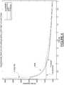
- the diode array 12 is able to provide a minimum power density of about 10kW/cm 2 and maximum > 100 kW/cm 2 at two percent duty cycle. This makes it feasible to generate sufficient optical power to melt a wide variety of materials.
- Figure 3 provides a table of the average power flux that has been calculated to melt various types of materials.
- Figure 4 shows a graph that illustrates the effectiveness of the diode array 12 on a variety of metal powders (i.e., Aluminum, Titanium, Iron and Tungsten), at a power flux sufficient to melt all the materials. The calculations to obtain the graphs shown in Figure 4 were performed in MATLAB with conductive and radiative losses taken into account. A conservative 30% absorptivity was assumed along with a powder layer thickness of 100 ⁇ m.
- diode arrays comprised of one or more diode bars
- the diode array 12 may be constructed to have a one square meter area, which would allow correspondingly large scale components to be constructed through an AM fabrication process, provided of course that a suitably sized powder bed is available to support fabrication of the part.
- the system 10 can be integrated into existing AM fabrication systems with the added benefit of no moving parts.
- the system 10 allows for the AM fabrication of traditionally difficult to fabricate and join metal such as ODS (oxide dispersion strengthened) steels or any alloy traditionally formed using solid state (i.e. non-melt) processing techniques.
- the mask 14 forms a "liquid crystal polarization rotator" comprised of a liquid crystal module (LCM) 14a and a polarizing element 14b, in this example a polarizing mirror (hereinafter "polarizing mirror” 14b).
- the polarizing mirror 14b directs the light defined by the liquid crystal polarization rotator and shapes the optical pattern that irradiates the substrate 20.
- the LCM 14a that helps to form the mask 14 may is up of one or more two dimensional, electronically (i.e., digitally) addressable arrays of pixels.
- Liquid crystal polarizers are commercially available and form two dimensional arrays of addressable pixels which work by changing the polarity of an incoming photon that is then rejected by a polarization element.
- the polarizing element 14b forms a discrete component of the mask 14 that is used to help focus and/or shape the optical signal.
- a first layer of powdered material is acted on by the system by pulsing the diode array 12 to melt selected portions (or possibly the entire portion) of the first layer.
- a subsequent (i.e., second) layer of powdered material is added over the layer just acted on by the system 10 and the process is repeated.
- the diode array 12 is pulsed to melt one or more selected subportions (or possibly the entirety) of the second layer of material.
- the system 10 electronically controls the pixels of the mask 14 to selectively block specific, predetermined portions of the substrate 20 from being irradiated by the pulsed optical signal from the diode array 12.
- This process is repeated for each layer, with the computer 18 controlling the mask 14 so that, for each layer, one or more selected subportions (or possibly the entirety) of the powdered material is blocked by the mask 14 from being exposed to the pulsed optical signal.
- the computer 18 controlling the mask 14 so that, for each layer, one or more selected subportions (or possibly the entirety) of the powdered material is blocked by the mask 14 from being exposed to the pulsed optical signal.
- an entire two dimensional area of each layer is melted or sintered at once by pulsing the diode array 12.
- System 100 includes a diode array 102 and a diode relay telescope 104.
- the diode relay telescope 104 is used to provide digital control over "tiles" within an array image to the "pixels" in the substrate 20 (powder bed).
- Figure 6 illustrates a system 200 having a diode array 202 and a plurality of focusing lenses 206 that are used to focus the optical energy from the array onto a corresponding plurality of "sheets" representing the substrate 20.
- the systems 10, 100 and 200 are able to melt and sinter each layer in a single "pass" or, put differently, in a single operation by pulsing the diode array 12.
- the need to raster scan an optical beam dozens, hundreds or more times, back and forth across a surface, is therefore eliminated. This significantly reduces the time required to melt and sinter each layer of powder material during the AM fabrication process.
- Nozzles 301, 302, and 303 are capable of depositing layers of different material powders 304 onto the substrate 20.
- the nozzle heads 301, 302 and 303 are rastered across the part surface covering it with material addressed by a programmable source. Both the irradiation from the diode array 12 and operation of the mask 14, as described in connection with the system 10, can be controlled such that each material deposited from the nozzles 301, 302 and 303 receives the correct amount of optical energy for a controlled melt or sintering.
Landscapes
- Engineering & Computer Science (AREA)
- Physics & Mathematics (AREA)
- Optics & Photonics (AREA)
- Chemical & Material Sciences (AREA)
- Materials Engineering (AREA)
- Manufacturing & Machinery (AREA)
- Plasma & Fusion (AREA)
- Mechanical Engineering (AREA)
- Health & Medical Sciences (AREA)
- General Health & Medical Sciences (AREA)
- Toxicology (AREA)
- Automation & Control Theory (AREA)
- Metallurgy (AREA)
- Organic Chemistry (AREA)
- Powder Metallurgy (AREA)
- General Physics & Mathematics (AREA)
Description
- The present disclosure relates to Additive Manufacturing systems and techniques for making three dimensional articles and parts, and more particularly to a system and method for performing Additive Manufacturing using a high power diode system.
- The statements in this section merely provide background information related to the present disclosure and may not constitute prior art.
- Additive Manufacturing ("AM"), also referred to as 3D printing, is a manufacturing technique in which material is added sequentially, layer by layer, in order to build a part. This is in contrast to traditional machining, where the part starts as a block of material that is then whittled down to the final desired shape. With AM fabrication, a directed power source is used to agglomerate material (typically powder) into a final, near net-shape article. Three dimensional articles are manufactured one layer at a time as an assemblage of two-dimensional sections. One important advantage of AM fabrication is that complex shapes (e.g. parts with internal features) can be realized. Another important advantage is that the material required is limited to that used to form the final part. Thus, AM fabrication has the benefit of very little material loss. This is especially important for expensive/tightly controlled materials.
- The use of AM for metal fabrication is relatively recent. Historically, plastics have been the focus of commercial systems that employ AM. Nevertheless, the use of metals with AM is highly commercially and technologically important because the majority of engineered structures rely heavily on metals. Metal AM requires a relatively high power, highly focused laser beam (typically on the order of 100W-1000W) to melt, fuse, and/or sinter metallic powder. The metal powder is typically placed in a powder bed during the AM process. The laser beam is rastered along the powder surface to make a two-dimensional section per pass. Once each layer is completed, the powder bed retracts and new powder is layered on top of the just-completed layer. Considering that a typical layer thickness is only about 50-100 microns, it can be seen how this rastering is the most time consuming step. This is the principal reason why objects that would only take two to three hours to machine using traditional machining methods may take up to eight hours or more using AM. Moreover, due to the necessity of rastering the laser beam, the maximum part size can be limited. Presently a 25cmx25cm area part size is the largest part size that can be made with an AM technique that involves rastering the laser beam. Accordingly, there is a strong desire to reduce the time required to manufacture objects, and particularly metal objects, using AM. One important challenge that the present disclosure addresses is overcoming this relatively slow speed necessitated by the raster scanning operation employed with a conventional AM fabrication process.
-
US 2011/0190904 A1 provides a method and a system for fabricating multimaterial bodies in a layer-wise fashion. These bodies may be used for bone stabilizing implants. A conventional mask to block certain portions of optical energy from reaching the beneath layer of material is furthermore disclosed. -
US 2009/020901 A1 relates to the additive manufacture of parts in powder beds, wherein a LCD mask for directing energy beam radiations at desired locations to melt the powder might be used. -
US 2004/0200812 A1 teaches a laser imaging apparatus having a laser source outputting a laser beam and an electronic display device. The electronic display device is positioned downstream from the laser source and operable to selectively polarize parts of the laser beam. - The present invention relates to a system for performing an Additive Manufacturing (AM) fabrication process on a powdered material forming a substrate according to
claim 1. The system comprises a diode array for generating an optical signal sufficient to melt or sinter a powdered material of the substrate. A mask is used for preventing a first predetermined portion of the optical signal from reaching the substrate, while allowing a second predetermined portion to reach the substrate. At least one processor is used for controlling an output of the diode array. - The present disclosure further relates to a system for performing an Additive Manufacturing (AM) fabrication process on a powdered material forming a substrate. The system comprises a diode array for generating a pulsed optical signal sufficient in optical intensity to melt or sinter a powdered material of the substrate. A mask is interposed between the diode array and the substrate for preventing a first predetermined portion of the pulsed optical signal from reaching the substrate, while allowing a second predetermined portion to reach the substrate. The mask is configured to be controlled and addressable by a processor to electronically enable selected subportions of the substrate to be masked off. A processor is used for electronically controlling the mask.
- In another aspect the present disclosure relates to a method for performing Additive Manufacturing (AM). The method comprises irradiating a powdered layer of a substrate using a pulsed optical signal sufficient to irradiate at least a substantial portion of an entire two dimensional layer within which the substrate is positioned. A mask is used to selectively block a first subportion of the pulsed optical signal from reaching the first layer of the substrate. A second layer of powdered material is placed over the first layer. The second layer is irradiated using the pulsed optical signal while using the mask to selectively block a second subportion of the pulsed optical signal from reaching the second layer of the substrate.
- Further areas of applicability will become apparent from the description provided herein. It should be understood that the description and specific examples are intended for purposes of illustration only and are not intended to limit the scope of the present disclosure.
- The drawings described herein are for illustration purposes only and are not intended to limit the scope of the present disclosure in any way. In the drawings:
-
Figure 1 is a diagrammatic view one embodiment of the present system and method for performing an Additive Manufacturing ("AM") fabrication process using a high power diode array and a mask; -
Figure 2 is a diagrammatic side view of the system ofFigure 1 showing how a portion of the optical rays from the diode array are reflected by a polarizing mirror during the fabrication process to prevent them from reaching the substrate; -
Figure 3 is a chart illustrating the average power flux required to melt various types of metals; -
Figure 4 is a graph that shows a plurality of curves representing various temperatures required to melt various materials, along with the time required to melt each material; -
Figure 5 shows an alternative form of the system of the present disclosure in which distinct "tiles" (predetermined areas) corresponding to pixels of the substrate are digitally controlled during the AM fabrication process; -
Figure 6 is another alternative form of the system of the present disclosure in which a plurality of focusing lenses are used to simultaneously focus the output from the diode array onto specific sections of the substrate for simultaneously melting distinct, separate sheets of material; and -
Figure 7 is a diagrammatic side view of a method of deposition of different material types in powder form prior to illumination by diode array generated light to melt/sinter the dissimilar powders together. - The following description is merely exemplary in nature and is not intended to limit the present disclosure, application, or uses. It should be understood that throughout the drawings, corresponding reference numerals indicate like or corresponding parts and features.
- Referring to
Figure 1 asystem 10 is shown in accordance with one embodiment of the present disclosure for performing an Additive Manufacturing ("AM") fabrication process. Thesystem 10 includes a highpower diode array 12 and a computer controlled, selective area mask 14 (hereinafter simply "mask 14"). A suitable power supply 16 may be used for providing electrical power to thediode array 12. Acomputer 18 or other suitable form of processor or controller is used for controlling the power supply 16 to control the on/off application of power to thediode array 12 as well as selectively (i.e., digitally) controlling themask 14 and shaping or focusing the optical beam. Optionally, separate processors or computers may be used to control thediode array 12 and themask 14. Selectively electronically controlling themask 14 with thecomputer 18 allows the optical beam from thediode array 12 to be prevented from reaching specific selected portions of powder that forms a substrate 20 (i.e., powder bed) so that those portions are not irradiated by the beam. InFigure 1 portion 15 is cross hatched to represent a portion of the output from thediode array 12 that does not reach the powdered material of thesubstrate 20. - In one preferred form the
diode array 12 may comprise a single large diode bar. Alternatively a plurality of diode bars located adjacent one another may be used to form thediode array 12. In one preferred form the diode array may be made up of arrays of diode bars each being about 1cm x 0.015cm to construct a 25cm x 25cm diode array. However, any number of diode bars may be used, and the precise number and configuration may depend on the part being constructed as well as other factors. Suitable diode bars for forming thediode array 12 are available from Lasertel of Tucson, AZ, Oclaro Inc. of San Jose, CA, nLight Corp. of Vancouver, WA, Quantel Inc. of New York, NY, DILAS Diode Laser, Inc. of Tucson, AZ, and Jenoptik AG of Jena, Germany, as well as many others. Thediode array 12 is able to provide a minimum power density of about 10kW/cm2 and maximum > 100 kW/cm2 at two percent duty cycle. This makes it feasible to generate sufficient optical power to melt a wide variety of materials.Figure 3 provides a table of the average power flux that has been calculated to melt various types of materials.Figure 4 shows a graph that illustrates the effectiveness of thediode array 12 on a variety of metal powders (i.e., Aluminum, Titanium, Iron and Tungsten), at a power flux sufficient to melt all the materials. The calculations to obtain the graphs shown inFigure 4 were performed in MATLAB with conductive and radiative losses taken into account. A conservative 30% absorptivity was assumed along with a powder layer thickness of 100µm. - It will also be appreciated that a significant advantage of using a diode array comprised of one or more diode bars is that such an assembly is readily scalable. Thus, diode arrays of various sizes can be constructed to meet the needs of making a specific sized part. For example, the
diode array 12 may be constructed to have a one square meter area, which would allow correspondingly large scale components to be constructed through an AM fabrication process, provided of course that a suitably sized powder bed is available to support fabrication of the part. Another significant advantage is that thesystem 10 can be integrated into existing AM fabrication systems with the added benefit of no moving parts. Thesystem 10 allows for the AM fabrication of traditionally difficult to fabricate and join metal such as ODS (oxide dispersion strengthened) steels or any alloy traditionally formed using solid state (i.e. non-melt) processing techniques. - Referring to
Figure 2 , themask 14 forms a "liquid crystal polarization rotator" comprised of a liquid crystal module (LCM) 14a and apolarizing element 14b, in this example a polarizing mirror (hereinafter "polarizing mirror" 14b). Thepolarizing mirror 14b directs the light defined by the liquid crystal polarization rotator and shapes the optical pattern that irradiates thesubstrate 20. The LCM 14a that helps to form themask 14 may is up of one or more two dimensional, electronically (i.e., digitally) addressable arrays of pixels. Liquid crystal polarizers are commercially available and form two dimensional arrays of addressable pixels which work by changing the polarity of an incoming photon that is then rejected by a polarization element. However, with thesystem 10, thepolarizing element 14b forms a discrete component of themask 14 that is used to help focus and/or shape the optical signal. - In
Figure 2 themask 14 receives light 22 being output from thediode array 12 as the light irradiates the LCM 14a. Pixels of the LCM 14a are independently addressed using thecomputer 18 to reject light at specific select areas of thesubstrate 20. Using the LCM 14a and thepolarizing mirror 14b to form themask 14 enables the light generated by thediode array 12 to be controllably directed onto only selected areas of thesubstrate 20 as needed. InFigure 2 light indicated bylines 22a is able to pass through thepolarizing mirror 14b while light indicated bylines 22b is rejected by the polarizing mirror. An important advantage of using a computer controlled LCM 14a is that only a very small amount of optical energy is absorbed into thepolarizing mirror 14b, thus making it feasible to prevent damage to the mirror. - During an actual AM fabrication operation, a first layer of powdered material is acted on by the system by pulsing the
diode array 12 to melt selected portions (or possibly the entire portion) of the first layer. A subsequent (i.e., second) layer of powdered material is added over the layer just acted on by thesystem 10 and the process is repeated. Thediode array 12 is pulsed to melt one or more selected subportions (or possibly the entirety) of the second layer of material. With each layer thesystem 10 electronically controls the pixels of themask 14 to selectively block specific, predetermined portions of thesubstrate 20 from being irradiated by the pulsed optical signal from thediode array 12. This process is repeated for each layer, with thecomputer 18 controlling themask 14 so that, for each layer, one or more selected subportions (or possibly the entirety) of the powdered material is blocked by themask 14 from being exposed to the pulsed optical signal. Preferably, an entire two dimensional area of each layer is melted or sintered at once by pulsing thediode array 12. However, it is just as feasible to raster scan thediode array 12 over the two dimensional area in the event the entire two dimensional area cannot be completely irradiated by the diode array. - Referring to
Figures 5 and 6 , twoalternative systems System 100 includes adiode array 102 and adiode relay telescope 104. Thediode relay telescope 104 is used to provide digital control over "tiles" within an array image to the "pixels" in the substrate 20 (powder bed).Figure 6 illustrates asystem 200 having adiode array 202 and a plurality of focusinglenses 206 that are used to focus the optical energy from the array onto a corresponding plurality of "sheets" representing thesubstrate 20. - The
systems diode array 12. The need to raster scan an optical beam dozens, hundreds or more times, back and forth across a surface, is therefore eliminated. This significantly reduces the time required to melt and sinter each layer of powder material during the AM fabrication process. - Referring to
Figure 7 , a method of deposition of different material types in powder form is illustrated insystem 300.Nozzles different material powders 304 onto thesubstrate 20. The nozzle heads 301, 302 and 303 are rastered across the part surface covering it with material addressed by a programmable source. Both the irradiation from thediode array 12 and operation of themask 14, as described in connection with thesystem 10, can be controlled such that each material deposited from thenozzles - While various embodiments have been described, those skilled in the art will recognize modifications or variations which might be made without departing from the present disclosure. The examples illustrate the various embodiments and are not intended to limit the present disclosure.
Claims (8)
- A system for performing an Additive Manufacturing (AM) fabrication process on a powdered material forming a substrate, the system comprising:a diode array for generating an optical signal sufficient to melt or sinter a powdered material of the substrate;a mask for receiving the optical signal generated by the diode array, the mask forming a liquid crystal polarization rotator, the liquid crystal polarization rotator including a liquid crystal module and a polarizer, wherein the liquid crystal module operates to receive and to rotate a first portion of the optical signal passing therethrough while allowing a second portion of the optical signal to pass therethrough without being rotated, and wherein the polarizer, which comprises a polarizing mirror, operates to reject by reflecting one of the first or second portions of the optical signal received from the liquid crystal module, and thus to prevent the one of the first or second portions from reaching the substrate, while the polarizer allows the other one of the first or second portions of the optical signal to reach the substrate, the liquid crystal module of the mask having a plurality of pixels arranged in a two dimensional pattern that are individually controlled to enable the mask to mask off one or more selected areas of a specific layer of the powdered material of the substrate, and wherein the mask absorbs substantially no optical energy from the optical signal; andat least one processor controlling an output of the diode array and assisting in controlling operation of the mask such that only selected one of the pixels are controlled to enable portions of the optical signal passing through the liquid crystal polarization rotator to be rotated to thus form the first portion of the optical signal; andwherein the diode array is configured to provide a power density of at least about 10kW/cm2 at a two percent duty cycle.
- The system of claim 1,
wherein the diode array comprises a plurality of diode bars. - The system of claim 1,
wherein the liquid crystal module comprises a computer controllable liquid crystal module configured to be digitally controlled by the processor. - A method for performing Additive Manufacturing (AM) comprising:irradiating a powdered layer of a substrate using a pulsed optical signal from a diode array which is sufficient to irradiate at least a substantial portion of an entire two dimensional area within which the substrate is positioned, and wherein the diode provides a power density of at least about 10kW/cm2 at a two percent duty cycle;using a mask to selectively block a first subportion of the pulsed optical signal from the first layer of the substrate, to thus prevent the first subportion from reaching the first layer of the substrate;placing a second layer of powdered material over the first layer; andirradiating the second layer using the pulsed optical signal while using the mask to selectively block a second subportion of the pulsed optical signal from reaching the second layer of the substratewherein the using a digitally electronically addressable mask comprises using a liquid crystal module and a polarizing element whereinthe liquid crystal module operates to receive and to rotate a first subportion of the pulsed optical signal passing therethrough while allowing a second subportion of the pulsed optical signal to pass therethrough without being rotated, and wherein the polarizer, which comprises a polarizing mirror, operates to reject by reflecting one of the first or second subportions of the pulsed optical signal received from the liquid crystal module, and thus to prevent the one of the first or second subportions from reaching the substrate, while the polarizer allows the other one of the first or second subportions of the pulsed optical signal to reach the substrate.
- The method of claim 4,
further comprising using a computer to control the digitally electronically addressable mask. - The method of claim 4,
further comprising using a computer to control the pulsed diode array. - The method of claim 4,
further comprising using a movable, electronically addressable spray source to deposit at least two different material types to form at least one of the first and second layers. - The method of claim 7,
further comprising controlling the mask in accordance with the at least two different material types being irradiated.
Applications Claiming Priority (2)
| Application Number | Priority Date | Filing Date | Title |
|---|---|---|---|
| US13/785,484 US9308583B2 (en) | 2013-03-05 | 2013-03-05 | System and method for high power diode based additive manufacturing |
| PCT/US2014/020638 WO2014138192A1 (en) | 2013-03-05 | 2014-03-05 | System and method for high power diode based additive manufacturing |
Publications (3)
| Publication Number | Publication Date |
|---|---|
| EP2964418A1 EP2964418A1 (en) | 2016-01-13 |
| EP2964418A4 EP2964418A4 (en) | 2016-11-23 |
| EP2964418B1 true EP2964418B1 (en) | 2019-05-08 |
Family
ID=51486905
Family Applications (1)
| Application Number | Title | Priority Date | Filing Date |
|---|---|---|---|
| EP14760359.1A Active EP2964418B1 (en) | 2013-03-05 | 2014-03-05 | System and method for high power diode based additive manufacturing |
Country Status (7)
| Country | Link |
|---|---|
| US (5) | US9308583B2 (en) |
| EP (1) | EP2964418B1 (en) |
| JP (2) | JP6412514B2 (en) |
| KR (3) | KR20230100754A9 (en) |
| ES (1) | ES2736040T3 (en) |
| IL (1) | IL241197B (en) |
| WO (1) | WO2014138192A1 (en) |
Cited By (5)
| Publication number | Priority date | Publication date | Assignee | Title |
|---|---|---|---|---|
| US10518328B2 (en) | 2015-10-30 | 2019-12-31 | Seurat Technologies, Inc. | Additive manufacturing system and method |
| US11014302B2 (en) | 2017-05-11 | 2021-05-25 | Seurat Technologies, Inc. | Switchyard beam routing of patterned light for additive manufacturing |
| US11148319B2 (en) | 2016-01-29 | 2021-10-19 | Seurat Technologies, Inc. | Additive manufacturing, bond modifying system and method |
| US11541481B2 (en) | 2018-12-19 | 2023-01-03 | Seurat Technologies, Inc. | Additive manufacturing system using a pulse modulated laser for two-dimensional printing |
| US11701819B2 (en) | 2016-01-28 | 2023-07-18 | Seurat Technologies, Inc. | Additive manufacturing, spatial heat treating system and method |
Families Citing this family (59)
| Publication number | Priority date | Publication date | Assignee | Title |
|---|---|---|---|---|
| US9308583B2 (en) | 2013-03-05 | 2016-04-12 | Lawrence Livermore National Security, Llc | System and method for high power diode based additive manufacturing |
| US10562132B2 (en) | 2013-04-29 | 2020-02-18 | Nuburu, Inc. | Applications, methods and systems for materials processing with visible raman laser |
| US10971896B2 (en) | 2013-04-29 | 2021-04-06 | Nuburu, Inc. | Applications, methods and systems for a laser deliver addressable array |
| GB201310398D0 (en) | 2013-06-11 | 2013-07-24 | Renishaw Plc | Additive manufacturing apparatus and method |
| EP3007879B1 (en) * | 2013-06-10 | 2019-02-13 | Renishaw Plc. | Selective laser solidification apparatus and method |
| US20150132173A1 (en) * | 2013-11-12 | 2015-05-14 | Siemens Energy, Inc. | Laser processing of a bed of powdered material with variable masking |
| US20160303798A1 (en) * | 2013-12-20 | 2016-10-20 | United Technologies Corporation | Method and device for manufacturing of three dimensional objects utilizing direct plasma arc |
| US9815139B2 (en) * | 2014-01-22 | 2017-11-14 | Siemens Energy, Inc. | Method for processing a part with an energy beam |
| GB2546016B (en) | 2014-06-20 | 2018-11-28 | Velo3D Inc | Apparatuses, systems and methods for three-dimensional printing |
| US11646549B2 (en) | 2014-08-27 | 2023-05-09 | Nuburu, Inc. | Multi kW class blue laser system |
| US10737324B2 (en) * | 2014-10-02 | 2020-08-11 | Lawrence Livermore National Security, Llc | System and method for forming material substrate printer |
| GB201505458D0 (en) | 2015-03-30 | 2015-05-13 | Renishaw Plc | Additive manufacturing apparatus and methods |
| CN107635749A (en) | 2015-06-10 | 2018-01-26 | Ipg光子公司 | Multiple beam increasing material manufacturing |
| CN104959602B (en) * | 2015-07-11 | 2017-12-29 | 新疆熠金能源科技有限公司 | Utilize the dot matrix 3D printing light source of light emitting diode |
| US10220471B2 (en) | 2015-10-14 | 2019-03-05 | Lawrence Livermore National Security, Llc | Spatter reduction laser scanning strategy in selective laser melting |
| US20210053280A1 (en) * | 2015-10-30 | 2021-02-25 | Seurat Technologies, Inc. | Electron Beam Patterning System In Additive Manufacturing |
| WO2017079091A1 (en) | 2015-11-06 | 2017-05-11 | Velo3D, Inc. | Adept three-dimensional printing |
| DE102015119745A1 (en) * | 2015-11-16 | 2017-05-18 | Cl Schutzrechtsverwaltungs Gmbh | Device for the generative production of a three-dimensional object |
| CN105312572B (en) * | 2015-11-17 | 2017-05-17 | 北京科技大学 | Molten iron alloy low-gravity 3D printing method and device |
| CN108698126A (en) | 2015-12-10 | 2018-10-23 | 维洛3D公司 | Consummate 3 D-printing |
| FR3046095B1 (en) | 2015-12-23 | 2018-01-26 | Addup | ADDITIVE MANUFACTURING MACHINE AND ADDITIVE MANUFACTURING METHOD USING SUCH A MACHINE |
| FR3046094A1 (en) * | 2015-12-23 | 2017-06-30 | Michelin & Cie | PROCESS FOR THE ADDITIVE MANUFACTURE OF A PIECE BY TOTAL OR PARTIAL SELECTIVE FUSION OF A POWDER AND MACHINE SUITABLE FOR THE IMPLEMENTATION OF SUCH A METHOD |
| US20170216971A1 (en) * | 2016-01-28 | 2017-08-03 | Lawrence Livermore National Security, Llc | Use of variable wavelength laser energy for custom additive manufacturing |
| US10618111B2 (en) * | 2016-01-28 | 2020-04-14 | Lawrence Livermore National Security, Llc | Heat treatment to anneal residual stresses during additive manufacturing |
| US10747033B2 (en) | 2016-01-29 | 2020-08-18 | Lawrence Livermore National Security, Llc | Cooler for optics transmitting high intensity light |
| WO2017143077A1 (en) | 2016-02-18 | 2017-08-24 | Velo3D, Inc. | Accurate three-dimensional printing |
| WO2017177310A1 (en) * | 2016-04-12 | 2017-10-19 | Magna International Inc. | High-power dynamic lens |
| US20220072659A1 (en) * | 2016-04-29 | 2022-03-10 | Nuburu, Inc. | Methods and Systems for Reducing Hazardous Byproduct from Welding Metals Using Lasers |
| US11612957B2 (en) * | 2016-04-29 | 2023-03-28 | Nuburu, Inc. | Methods and systems for welding copper and other metals using blue lasers |
| EP3492244A1 (en) | 2016-06-29 | 2019-06-05 | VELO3D, Inc. | Three-dimensional printing system and method for three-dimensional printing |
| US11691343B2 (en) | 2016-06-29 | 2023-07-04 | Velo3D, Inc. | Three-dimensional printing and three-dimensional printers |
| CN107866567B (en) * | 2016-09-28 | 2019-09-13 | 中国航空制造技术研究院 | The more laser of large format based on powder bed increasing material manufacturing become junction scan method |
| US10661341B2 (en) | 2016-11-07 | 2020-05-26 | Velo3D, Inc. | Gas flow in three-dimensional printing |
| US10611092B2 (en) | 2017-01-05 | 2020-04-07 | Velo3D, Inc. | Optics in three-dimensional printing |
| GB201700170D0 (en) * | 2017-01-06 | 2017-02-22 | Rolls Royce Plc | Manufacturing method and apparatus |
| US10583530B2 (en) | 2017-01-09 | 2020-03-10 | General Electric Company | System and methods for fabricating a component with laser array |
| US10919286B2 (en) * | 2017-01-13 | 2021-02-16 | GM Global Technology Operations LLC | Powder bed fusion system with point and area scanning laser beams |
| JP6911153B2 (en) | 2017-01-31 | 2021-07-28 | ヌブル インク | Methods and systems for welding copper using a blue laser |
| US10369629B2 (en) | 2017-03-02 | 2019-08-06 | Veo3D, Inc. | Three-dimensional printing of three-dimensional objects |
| US20180281237A1 (en) | 2017-03-28 | 2018-10-04 | Velo3D, Inc. | Material manipulation in three-dimensional printing |
| US10471508B2 (en) | 2017-03-28 | 2019-11-12 | GM Global Technology Operations LLC | Additive manufacturing with laser energy recycling |
| CN110267757B (en) * | 2017-04-10 | 2022-04-19 | 惠普发展公司,有限责任合伙企业 | Reducing stress in metal layers |
| KR102423330B1 (en) | 2017-04-21 | 2022-07-20 | 누부루 인크. | Multi-Coated Fiber |
| CN107099717B (en) * | 2017-05-16 | 2018-11-09 | 北京科技大学 | The technology of preparing of crystal boundary auto purification tungsten magnesium alloy |
| JP2020523793A (en) | 2017-06-13 | 2020-08-06 | ヌブル インク | Ultra-dense wavelength beam-coupled laser system |
| US10597073B2 (en) | 2017-06-19 | 2020-03-24 | GM Global Technology Operations LLC | Vehicles and steering systems for vehicles providing haptic feedback |
| US10766242B2 (en) * | 2017-08-24 | 2020-09-08 | General Electric Company | System and methods for fabricating a component using a consolidating device |
| US11084132B2 (en) * | 2017-10-26 | 2021-08-10 | General Electric Company | Diode laser fiber array for contour of powder bed fabrication or repair |
| US10272525B1 (en) | 2017-12-27 | 2019-04-30 | Velo3D, Inc. | Three-dimensional printing systems and methods of their use |
| US10144176B1 (en) | 2018-01-15 | 2018-12-04 | Velo3D, Inc. | Three-dimensional printing systems and methods of their use |
| US11167375B2 (en) | 2018-08-10 | 2021-11-09 | The Research Foundation For The State University Of New York | Additive manufacturing processes and additively manufactured products |
| WO2020107030A1 (en) | 2018-11-23 | 2020-05-28 | Nuburu, Inc | Multi-wavelength visible laser source |
| CN109623098A (en) * | 2018-12-23 | 2019-04-16 | 南京理工大学 | A kind of compound increasing material method of MIG-TIG |
| CN109623097A (en) * | 2018-12-23 | 2019-04-16 | 南京理工大学 | A kind of compound increasing material device of MIG-TIG |
| EP3917718A4 (en) | 2019-02-02 | 2022-12-07 | Nuburu, Inc. | High reliability high power, high brightness blue laser diode systems and methods of making |
| US11407172B2 (en) | 2020-03-18 | 2022-08-09 | Powder Motion Labs, LLC | Recoater using alternating current to planarize top surface of powder bed |
| US11612940B2 (en) | 2020-03-18 | 2023-03-28 | Powder Motion Labs, LLC | Powder bed recoater |
| US20230037200A1 (en) | 2021-07-28 | 2023-02-02 | DePuy Synthes Products, Inc. | 3D-Printed Implants And Methods For 3D Printing Of Implants |
| TW202321012A (en) * | 2021-11-19 | 2023-06-01 | 國立臺灣科技大學 | High-speed additive manufacturing apparatus |
Family Cites Families (38)
| Publication number | Priority date | Publication date | Assignee | Title |
|---|---|---|---|---|
| US4247508B1 (en) | 1979-12-03 | 1996-10-01 | Dtm Corp | Molding process |
| US5236637A (en) | 1984-08-08 | 1993-08-17 | 3D Systems, Inc. | Method of and apparatus for production of three dimensional objects by stereolithography |
| US5296062A (en) | 1986-10-17 | 1994-03-22 | The Board Of Regents, The University Of Texas System | Multiple material systems for selective beam sintering |
| ATE138294T1 (en) * | 1986-10-17 | 1996-06-15 | Univ Texas | METHOD AND DEVICE FOR PRODUCING SINTERED MOLDED BODIES BY PARTIAL INTERNATION |
| US4944817A (en) | 1986-10-17 | 1990-07-31 | Board Of Regents, The University Of Texas System | Multiple material systems for selective beam sintering |
| JP2728537B2 (en) * | 1990-03-07 | 1998-03-18 | 株式会社日立製作所 | Liquid crystal mask type laser marker |
| US5314003A (en) | 1991-12-24 | 1994-05-24 | Microelectronics And Computer Technology Corporation | Three-dimensional metal fabrication using a laser |
| JPH071593A (en) * | 1993-06-22 | 1995-01-06 | Hitachi Ltd | Optical molding apparatus |
| US5393482A (en) | 1993-10-20 | 1995-02-28 | United Technologies Corporation | Method for performing multiple beam laser sintering employing focussed and defocussed laser beams |
| JP3258480B2 (en) | 1994-01-27 | 2002-02-18 | キヤノン株式会社 | Process cartridge |
| US5674414A (en) | 1994-11-11 | 1997-10-07 | Carl-Zeiss Stiftung | Method and apparatus of irradiating a surface of a workpiece with a plurality of beams |
| US5640667A (en) | 1995-11-27 | 1997-06-17 | Board Of Regents, The University Of Texas System | Laser-directed fabrication of full-density metal articles using hot isostatic processing |
| CA2272629A1 (en) * | 1996-11-21 | 1998-05-28 | Thaumaturge Pty. Limited | Improved object manufacture |
| DE19649865C1 (en) | 1996-12-02 | 1998-02-12 | Fraunhofer Ges Forschung | Shaped body especially prototype or replacement part production |
| CA2227672A1 (en) * | 1997-01-29 | 1998-07-29 | Toyota Jidosha Kabushiki Kaisha | Method for producing a laminated object and apparatus for producing the same |
| GB9923954D0 (en) * | 1999-10-11 | 1999-12-08 | Foseco Int | Sintering of powder particles into granules |
| WO2002027408A2 (en) | 2000-09-27 | 2002-04-04 | The Regents Of The University Of California | Dynamic mask projection stereo micro lithography |
| US20020093115A1 (en) * | 2001-01-12 | 2002-07-18 | Jang B. Z. | Layer manufacturing method and apparatus using a programmable planar light source |
| US20040020081A1 (en) * | 2002-08-01 | 2004-02-05 | Symons Dominic Paul | Sport boot |
| US6867388B2 (en) * | 2003-04-08 | 2005-03-15 | Branson Ultrasonics Corporation | Electronic masking laser imaging system |
| TW594437B (en) * | 2003-10-16 | 2004-06-21 | Univ Nat Taiwan Science Tech | Dynamic mask module |
| US7570128B2 (en) * | 2004-07-22 | 2009-08-04 | Nxp B.V. | Integrated non-reciprocal component comprising a ferrite substrate |
| WO2008118263A1 (en) * | 2007-03-22 | 2008-10-02 | Stratasys, Inc. | Extrusion-based layered deposition systems using selective radiation exposure |
| ATE553910T1 (en) * | 2007-07-04 | 2012-05-15 | Envisiontec Gmbh | METHOD AND DEVICE FOR PRODUCING A THREE-DIMENSIONAL OBJECT |
| WO2009042671A1 (en) | 2007-09-24 | 2009-04-02 | The Board Of Trustees Of The University Of Illinois | Three-dimensional microfabricated bioreactors with embedded capillary network |
| JP4258567B1 (en) | 2007-10-26 | 2009-04-30 | パナソニック電工株式会社 | Manufacturing method of three-dimensional shaped object |
| US20100323301A1 (en) * | 2009-06-23 | 2010-12-23 | Huey-Ru Tang Lee | Method and apparatus for making three-dimensional parts |
| US8160113B2 (en) | 2009-07-21 | 2012-04-17 | Mobius Photonics, Inc. | Tailored pulse burst |
| WO2011082152A1 (en) * | 2009-12-30 | 2011-07-07 | Synthes Usa, Llc | Intergrated multi-material implants and methods of manufacture |
| FR2957479B1 (en) * | 2010-03-12 | 2012-04-27 | Commissariat Energie Atomique | PROCESS FOR TREATING A METAL CONTACT REALIZED ON A SUBSTRATE |
| JP5704315B2 (en) * | 2011-01-07 | 2015-04-22 | 株式会社ブイ・テクノロジー | Exposure equipment |
| US9283593B2 (en) | 2011-01-13 | 2016-03-15 | Siemens Energy, Inc. | Selective laser melting / sintering using powdered flux |
| JP2014510896A (en) * | 2011-03-11 | 2014-05-01 | インダージット・シン | Method and apparatus for plasma assisted laser cooking of food products |
| ES2681980T3 (en) * | 2011-06-28 | 2018-09-17 | Global Filtration Systems, A Dba Of Gulf Filtration Systems Inc. | Apparatus for forming three-dimensional objects using linear solidification |
| US8691333B2 (en) * | 2011-06-28 | 2014-04-08 | Honeywell International Inc. | Methods for manufacturing engine components with structural bridge devices |
| GB201114048D0 (en) | 2011-08-16 | 2011-09-28 | Intrinsiq Materials Ltd | Curing system |
| US9498920B2 (en) * | 2013-02-12 | 2016-11-22 | Carbon3D, Inc. | Method and apparatus for three-dimensional fabrication |
| US9308583B2 (en) | 2013-03-05 | 2016-04-12 | Lawrence Livermore National Security, Llc | System and method for high power diode based additive manufacturing |
-
2013
- 2013-03-05 US US13/785,484 patent/US9308583B2/en active Active
-
2014
- 2014-03-05 KR KR1020237021446A patent/KR20230100754A9/en not_active Application Discontinuation
- 2014-03-05 WO PCT/US2014/020638 patent/WO2014138192A1/en active Application Filing
- 2014-03-05 KR KR1020157027184A patent/KR102325267B1/en active IP Right Grant
- 2014-03-05 EP EP14760359.1A patent/EP2964418B1/en active Active
- 2014-03-05 ES ES14760359T patent/ES2736040T3/en active Active
- 2014-03-05 JP JP2015561587A patent/JP6412514B2/en active Active
- 2014-03-05 KR KR1020217036328A patent/KR102549015B1/en active IP Right Grant
-
2015
- 2015-09-06 IL IL241197A patent/IL241197B/en active IP Right Grant
-
2016
- 2016-01-05 US US14/988,190 patent/US9855625B2/en active Active
- 2016-05-03 US US15/145,402 patent/US10569363B2/en active Active
-
2018
- 2018-06-20 JP JP2018117005A patent/JP2018168471A/en not_active Abandoned
-
2019
- 2019-12-27 US US16/728,929 patent/US11534865B2/en active Active
-
2022
- 2022-10-20 US US17/969,741 patent/US20230123528A1/en active Pending
Non-Patent Citations (1)
| Title |
|---|
| None * |
Cited By (18)
| Publication number | Priority date | Publication date | Assignee | Title |
|---|---|---|---|---|
| US10967566B2 (en) | 2015-10-30 | 2021-04-06 | Seurat Technologies, Inc. | Chamber systems for additive manufacturing |
| US10596626B2 (en) | 2015-10-30 | 2020-03-24 | Seurat Technologies, Inc. | Additive manufacturing system and method |
| US10518328B2 (en) | 2015-10-30 | 2019-12-31 | Seurat Technologies, Inc. | Additive manufacturing system and method |
| US11072114B2 (en) | 2015-10-30 | 2021-07-27 | Seurat Technologies, Inc. | Variable print chamber walls for powder bed fusion additive manufacturing |
| US10843266B2 (en) | 2015-10-30 | 2020-11-24 | Seurat Technologies, Inc. | Chamber systems for additive manufacturing |
| US10870150B2 (en) | 2015-10-30 | 2020-12-22 | Seurat Technologies, Inc. | Long and high resolution structures formed by additive manufacturing techniques |
| US10960465B2 (en) | 2015-10-30 | 2021-03-30 | Seurat Technologies, Inc. | Light recycling for additive manufacturing optimization |
| US10960466B2 (en) | 2015-10-30 | 2021-03-30 | Seurat Technologies, Inc. | Polarization combining system in additive manufacturing |
| US11911964B2 (en) | 2015-10-30 | 2024-02-27 | Seurat Technologies, Inc. | Recycling powdered material for additive manufacturing |
| US10583484B2 (en) | 2015-10-30 | 2020-03-10 | Seurat Technologies, Inc. | Multi-functional ingester system for additive manufacturing |
| US10843265B2 (en) | 2015-10-30 | 2020-11-24 | Seurat Technologies, Inc. | Enclosed additive manufacturing system |
| US11691341B2 (en) | 2015-10-30 | 2023-07-04 | Seurat Technologies, Inc. | Part manipulation using printed manipulation points |
| US11292090B2 (en) | 2015-10-30 | 2022-04-05 | Seurat Technologies, Inc. | Additive manufacturing system and method |
| US11446774B2 (en) | 2015-10-30 | 2022-09-20 | Seurat Technologies, Inc. | Dynamic optical assembly for laser-based additive manufacturing |
| US11701819B2 (en) | 2016-01-28 | 2023-07-18 | Seurat Technologies, Inc. | Additive manufacturing, spatial heat treating system and method |
| US11148319B2 (en) | 2016-01-29 | 2021-10-19 | Seurat Technologies, Inc. | Additive manufacturing, bond modifying system and method |
| US11014302B2 (en) | 2017-05-11 | 2021-05-25 | Seurat Technologies, Inc. | Switchyard beam routing of patterned light for additive manufacturing |
| US11541481B2 (en) | 2018-12-19 | 2023-01-03 | Seurat Technologies, Inc. | Additive manufacturing system using a pulse modulated laser for two-dimensional printing |
Also Published As
| Publication number | Publication date |
|---|---|
| IL241197A0 (en) | 2015-11-30 |
| US10569363B2 (en) | 2020-02-25 |
| US20140252687A1 (en) | 2014-09-11 |
| US9308583B2 (en) | 2016-04-12 |
| KR20230100754A9 (en) | 2024-03-21 |
| JP6412514B2 (en) | 2018-10-31 |
| KR20210138125A (en) | 2021-11-18 |
| US9855625B2 (en) | 2018-01-02 |
| EP2964418A4 (en) | 2016-11-23 |
| KR102549015B1 (en) | 2023-06-28 |
| US20200139487A1 (en) | 2020-05-07 |
| US11534865B2 (en) | 2022-12-27 |
| US20160243652A1 (en) | 2016-08-25 |
| US20160129503A1 (en) | 2016-05-12 |
| US20230123528A1 (en) | 2023-04-20 |
| WO2014138192A9 (en) | 2014-10-09 |
| IL241197B (en) | 2019-07-31 |
| ES2736040T3 (en) | 2019-12-23 |
| EP2964418A1 (en) | 2016-01-13 |
| JP2016518516A (en) | 2016-06-23 |
| WO2014138192A1 (en) | 2014-09-12 |
| JP2018168471A (en) | 2018-11-01 |
| KR20230100754A (en) | 2023-07-05 |
| KR20150124993A (en) | 2015-11-06 |
| KR102325267B1 (en) | 2021-11-11 |
Similar Documents
| Publication | Publication Date | Title |
|---|---|---|
| EP2964418B1 (en) | System and method for high power diode based additive manufacturing | |
| EP3307526B1 (en) | Multiple beam additive manufacturing | |
| US9314972B2 (en) | Apparatus for additive layer manufacturing of an article | |
| AU2016273983A1 (en) | 3D printing device for producing a spatially extended product | |
| US20170173875A1 (en) | 3D printing device for producing a spatially extended product | |
| EP3944915A1 (en) | Laser array for laser powder bed fusion processing of metal alloys | |
| US20230330750A1 (en) | Method of operating an irradiation system, irradiation system and apparatus for producing a three-dimensional work piece with polarization control |
Legal Events
| Date | Code | Title | Description |
|---|---|---|---|
| PUAI | Public reference made under article 153(3) epc to a published international application that has entered the european phase |
Free format text: ORIGINAL CODE: 0009012 |
|
| 17P | Request for examination filed |
Effective date: 20150928 |
|
| AK | Designated contracting states |
Kind code of ref document: A1 Designated state(s): AL AT BE BG CH CY CZ DE DK EE ES FI FR GB GR HR HU IE IS IT LI LT LU LV MC MK MT NL NO PL PT RO RS SE SI SK SM TR |
|
| AX | Request for extension of the european patent |
Extension state: BA ME |
|
| RIN1 | Information on inventor provided before grant (corrected) |
Inventor name: FARMER, JOSEPH C. Inventor name: EL-DASHER, BASSEM S. Inventor name: TORRES, SHARON G. Inventor name: DEMUTH, JAMES A. Inventor name: BAYRAMIAN, ANDREW |
|
| DAX | Request for extension of the european patent (deleted) | ||
| A4 | Supplementary search report drawn up and despatched |
Effective date: 20161024 |
|
| RIC1 | Information provided on ipc code assigned before grant |
Ipc: G02F 1/1335 20060101ALI20161018BHEP Ipc: B23K 26/064 20140101ALI20161018BHEP Ipc: B23K 26/364 20140101ALI20161018BHEP Ipc: B22F 3/105 20060101ALI20161018BHEP Ipc: B23K 26/067 20060101ALI20161018BHEP Ipc: H01S 3/0941 20060101ALI20161018BHEP Ipc: B23K 26/359 20140101AFI20161018BHEP |
|
| STAA | Information on the status of an ep patent application or granted ep patent |
Free format text: STATUS: EXAMINATION IS IN PROGRESS |
|
| 17Q | First examination report despatched |
Effective date: 20180927 |
|
| REG | Reference to a national code |
Ref country code: DE Ref legal event code: R079 Ref document number: 602014046343 Country of ref document: DE Free format text: PREVIOUS MAIN CLASS: B23K0026359000 Ipc: B22F0003105000 |
|
| GRAP | Despatch of communication of intention to grant a patent |
Free format text: ORIGINAL CODE: EPIDOSNIGR1 |
|
| STAA | Information on the status of an ep patent application or granted ep patent |
Free format text: STATUS: GRANT OF PATENT IS INTENDED |
|
| RIC1 | Information provided on ipc code assigned before grant |
Ipc: B29C 64/153 20170101ALI20181122BHEP Ipc: C22C 32/00 20060101ALN20181122BHEP Ipc: B22F 3/105 20060101AFI20181122BHEP Ipc: B33Y 50/02 20150101ALN20181122BHEP Ipc: B33Y 30/00 20150101ALI20181122BHEP |
|
| RIC1 | Information provided on ipc code assigned before grant |
Ipc: B33Y 50/02 20150101ALN20181123BHEP Ipc: B22F 3/105 20060101AFI20181123BHEP Ipc: B33Y 30/00 20150101ALI20181123BHEP Ipc: C22C 32/00 20060101ALN20181123BHEP Ipc: B29C 64/153 20170101ALI20181123BHEP |
|
| INTG | Intention to grant announced |
Effective date: 20181219 |
|
| RIC1 | Information provided on ipc code assigned before grant |
Ipc: B29C 64/153 20170101ALI20181210BHEP Ipc: B22F 3/105 20060101AFI20181210BHEP Ipc: B33Y 50/02 20150101ALN20181210BHEP Ipc: B33Y 30/00 20150101ALI20181210BHEP Ipc: C22C 32/00 20060101ALN20181210BHEP |
|
| GRAS | Grant fee paid |
Free format text: ORIGINAL CODE: EPIDOSNIGR3 |
|
| GRAA | (expected) grant |
Free format text: ORIGINAL CODE: 0009210 |
|
| STAA | Information on the status of an ep patent application or granted ep patent |
Free format text: STATUS: THE PATENT HAS BEEN GRANTED |
|
| AK | Designated contracting states |
Kind code of ref document: B1 Designated state(s): AL AT BE BG CH CY CZ DE DK EE ES FI FR GB GR HR HU IE IS IT LI LT LU LV MC MK MT NL NO PL PT RO RS SE SI SK SM TR |
|
| REG | Reference to a national code |
Ref country code: GB Ref legal event code: FG4D |
|
| REG | Reference to a national code |
Ref country code: CH Ref legal event code: EP Ref country code: AT Ref legal event code: REF Ref document number: 1129417 Country of ref document: AT Kind code of ref document: T Effective date: 20190515 |
|
| REG | Reference to a national code |
Ref country code: DE Ref legal event code: R096 Ref document number: 602014046343 Country of ref document: DE |
|
| REG | Reference to a national code |
Ref country code: IE Ref legal event code: FG4D |
|
| REG | Reference to a national code |
Ref country code: SE Ref legal event code: TRGR |
|
| REG | Reference to a national code |
Ref country code: CH Ref legal event code: NV Representative=s name: BOGENSBERGER PATENT- AND MARKENBUERO DR. BURKH, LI |
|
| REG | Reference to a national code |
Ref country code: NL Ref legal event code: FP |
|
| REG | Reference to a national code |
Ref country code: LT Ref legal event code: MG4D |
|
| PG25 | Lapsed in a contracting state [announced via postgrant information from national office to epo] |
Ref country code: PT Free format text: LAPSE BECAUSE OF FAILURE TO SUBMIT A TRANSLATION OF THE DESCRIPTION OR TO PAY THE FEE WITHIN THE PRESCRIBED TIME-LIMIT Effective date: 20190908 Ref country code: AL Free format text: LAPSE BECAUSE OF FAILURE TO SUBMIT A TRANSLATION OF THE DESCRIPTION OR TO PAY THE FEE WITHIN THE PRESCRIBED TIME-LIMIT Effective date: 20190508 Ref country code: FI Free format text: LAPSE BECAUSE OF FAILURE TO SUBMIT A TRANSLATION OF THE DESCRIPTION OR TO PAY THE FEE WITHIN THE PRESCRIBED TIME-LIMIT Effective date: 20190508 Ref country code: NO Free format text: LAPSE BECAUSE OF FAILURE TO SUBMIT A TRANSLATION OF THE DESCRIPTION OR TO PAY THE FEE WITHIN THE PRESCRIBED TIME-LIMIT Effective date: 20190808 Ref country code: HR Free format text: LAPSE BECAUSE OF FAILURE TO SUBMIT A TRANSLATION OF THE DESCRIPTION OR TO PAY THE FEE WITHIN THE PRESCRIBED TIME-LIMIT Effective date: 20190508 Ref country code: LT Free format text: LAPSE BECAUSE OF FAILURE TO SUBMIT A TRANSLATION OF THE DESCRIPTION OR TO PAY THE FEE WITHIN THE PRESCRIBED TIME-LIMIT Effective date: 20190508 |
|
| PG25 | Lapsed in a contracting state [announced via postgrant information from national office to epo] |
Ref country code: GR Free format text: LAPSE BECAUSE OF FAILURE TO SUBMIT A TRANSLATION OF THE DESCRIPTION OR TO PAY THE FEE WITHIN THE PRESCRIBED TIME-LIMIT Effective date: 20190809 Ref country code: BG Free format text: LAPSE BECAUSE OF FAILURE TO SUBMIT A TRANSLATION OF THE DESCRIPTION OR TO PAY THE FEE WITHIN THE PRESCRIBED TIME-LIMIT Effective date: 20190808 Ref country code: RS Free format text: LAPSE BECAUSE OF FAILURE TO SUBMIT A TRANSLATION OF THE DESCRIPTION OR TO PAY THE FEE WITHIN THE PRESCRIBED TIME-LIMIT Effective date: 20190508 Ref country code: LV Free format text: LAPSE BECAUSE OF FAILURE TO SUBMIT A TRANSLATION OF THE DESCRIPTION OR TO PAY THE FEE WITHIN THE PRESCRIBED TIME-LIMIT Effective date: 20190508 |
|
| REG | Reference to a national code |
Ref country code: AT Ref legal event code: MK05 Ref document number: 1129417 Country of ref document: AT Kind code of ref document: T Effective date: 20190508 |
|
| REG | Reference to a national code |
Ref country code: ES Ref legal event code: FG2A Ref document number: 2736040 Country of ref document: ES Kind code of ref document: T3 Effective date: 20191223 |
|
| PG25 | Lapsed in a contracting state [announced via postgrant information from national office to epo] |
Ref country code: AT Free format text: LAPSE BECAUSE OF FAILURE TO SUBMIT A TRANSLATION OF THE DESCRIPTION OR TO PAY THE FEE WITHIN THE PRESCRIBED TIME-LIMIT Effective date: 20190508 Ref country code: DK Free format text: LAPSE BECAUSE OF FAILURE TO SUBMIT A TRANSLATION OF THE DESCRIPTION OR TO PAY THE FEE WITHIN THE PRESCRIBED TIME-LIMIT Effective date: 20190508 Ref country code: EE Free format text: LAPSE BECAUSE OF FAILURE TO SUBMIT A TRANSLATION OF THE DESCRIPTION OR TO PAY THE FEE WITHIN THE PRESCRIBED TIME-LIMIT Effective date: 20190508 Ref country code: CZ Free format text: LAPSE BECAUSE OF FAILURE TO SUBMIT A TRANSLATION OF THE DESCRIPTION OR TO PAY THE FEE WITHIN THE PRESCRIBED TIME-LIMIT Effective date: 20190508 Ref country code: RO Free format text: LAPSE BECAUSE OF FAILURE TO SUBMIT A TRANSLATION OF THE DESCRIPTION OR TO PAY THE FEE WITHIN THE PRESCRIBED TIME-LIMIT Effective date: 20190508 Ref country code: SK Free format text: LAPSE BECAUSE OF FAILURE TO SUBMIT A TRANSLATION OF THE DESCRIPTION OR TO PAY THE FEE WITHIN THE PRESCRIBED TIME-LIMIT Effective date: 20190508 |
|
| REG | Reference to a national code |
Ref country code: DE Ref legal event code: R097 Ref document number: 602014046343 Country of ref document: DE |
|
| PG25 | Lapsed in a contracting state [announced via postgrant information from national office to epo] |
Ref country code: SM Free format text: LAPSE BECAUSE OF FAILURE TO SUBMIT A TRANSLATION OF THE DESCRIPTION OR TO PAY THE FEE WITHIN THE PRESCRIBED TIME-LIMIT Effective date: 20190508 |
|
| PLBE | No opposition filed within time limit |
Free format text: ORIGINAL CODE: 0009261 |
|
| STAA | Information on the status of an ep patent application or granted ep patent |
Free format text: STATUS: NO OPPOSITION FILED WITHIN TIME LIMIT |
|
| PG25 | Lapsed in a contracting state [announced via postgrant information from national office to epo] |
Ref country code: TR Free format text: LAPSE BECAUSE OF FAILURE TO SUBMIT A TRANSLATION OF THE DESCRIPTION OR TO PAY THE FEE WITHIN THE PRESCRIBED TIME-LIMIT Effective date: 20190508 |
|
| 26N | No opposition filed |
Effective date: 20200211 |
|
| PG25 | Lapsed in a contracting state [announced via postgrant information from national office to epo] |
Ref country code: PL Free format text: LAPSE BECAUSE OF FAILURE TO SUBMIT A TRANSLATION OF THE DESCRIPTION OR TO PAY THE FEE WITHIN THE PRESCRIBED TIME-LIMIT Effective date: 20190508 |
|
| PG25 | Lapsed in a contracting state [announced via postgrant information from national office to epo] |
Ref country code: SI Free format text: LAPSE BECAUSE OF FAILURE TO SUBMIT A TRANSLATION OF THE DESCRIPTION OR TO PAY THE FEE WITHIN THE PRESCRIBED TIME-LIMIT Effective date: 20190508 |
|
| PG25 | Lapsed in a contracting state [announced via postgrant information from national office to epo] |
Ref country code: MC Free format text: LAPSE BECAUSE OF FAILURE TO SUBMIT A TRANSLATION OF THE DESCRIPTION OR TO PAY THE FEE WITHIN THE PRESCRIBED TIME-LIMIT Effective date: 20190508 |
|
| REG | Reference to a national code |
Ref country code: BE Ref legal event code: MM Effective date: 20200331 |
|
| PG25 | Lapsed in a contracting state [announced via postgrant information from national office to epo] |
Ref country code: LU Free format text: LAPSE BECAUSE OF NON-PAYMENT OF DUE FEES Effective date: 20200305 |
|
| PG25 | Lapsed in a contracting state [announced via postgrant information from national office to epo] |
Ref country code: BE Free format text: LAPSE BECAUSE OF NON-PAYMENT OF DUE FEES Effective date: 20200331 |
|
| PG25 | Lapsed in a contracting state [announced via postgrant information from national office to epo] |
Ref country code: MT Free format text: LAPSE BECAUSE OF FAILURE TO SUBMIT A TRANSLATION OF THE DESCRIPTION OR TO PAY THE FEE WITHIN THE PRESCRIBED TIME-LIMIT Effective date: 20190508 Ref country code: CY Free format text: LAPSE BECAUSE OF FAILURE TO SUBMIT A TRANSLATION OF THE DESCRIPTION OR TO PAY THE FEE WITHIN THE PRESCRIBED TIME-LIMIT Effective date: 20190508 |
|
| PG25 | Lapsed in a contracting state [announced via postgrant information from national office to epo] |
Ref country code: MK Free format text: LAPSE BECAUSE OF FAILURE TO SUBMIT A TRANSLATION OF THE DESCRIPTION OR TO PAY THE FEE WITHIN THE PRESCRIBED TIME-LIMIT Effective date: 20190508 Ref country code: IS Free format text: LAPSE BECAUSE OF FAILURE TO SUBMIT A TRANSLATION OF THE DESCRIPTION OR TO PAY THE FEE WITHIN THE PRESCRIBED TIME-LIMIT Effective date: 20190908 |
|
| PGFP | Annual fee paid to national office [announced via postgrant information from national office to epo] |
Ref country code: IE Payment date: 20230327 Year of fee payment: 10 Ref country code: FR Payment date: 20230328 Year of fee payment: 10 |
|
| PGFP | Annual fee paid to national office [announced via postgrant information from national office to epo] |
Ref country code: SE Payment date: 20230315 Year of fee payment: 10 Ref country code: IT Payment date: 20230321 Year of fee payment: 10 Ref country code: GB Payment date: 20230327 Year of fee payment: 10 Ref country code: DE Payment date: 20230329 Year of fee payment: 10 |
|
| P01 | Opt-out of the competence of the unified patent court (upc) registered |
Effective date: 20230522 |
|
| PGFP | Annual fee paid to national office [announced via postgrant information from national office to epo] |
Ref country code: ES Payment date: 20230403 Year of fee payment: 10 Ref country code: CH Payment date: 20230402 Year of fee payment: 10 |
|
| PGFP | Annual fee paid to national office [announced via postgrant information from national office to epo] |
Ref country code: NL Payment date: 20240326 Year of fee payment: 11 Ref country code: IE Payment date: 20240327 Year of fee payment: 11 |
|
| PGFP | Annual fee paid to national office [announced via postgrant information from national office to epo] |
Ref country code: DE Payment date: 20240327 Year of fee payment: 11 Ref country code: GB Payment date: 20240327 Year of fee payment: 11 |