EP2195865B1 - Radiation-emitting semi-conductor component and method for producing a radiation-emitting semiconductor component - Google Patents
Radiation-emitting semi-conductor component and method for producing a radiation-emitting semiconductor component Download PDFInfo
- Publication number
- EP2195865B1 EP2195865B1 EP08801325.5A EP08801325A EP2195865B1 EP 2195865 B1 EP2195865 B1 EP 2195865B1 EP 08801325 A EP08801325 A EP 08801325A EP 2195865 B1 EP2195865 B1 EP 2195865B1
- Authority
- EP
- European Patent Office
- Prior art keywords
- semiconductor
- based component
- glass substrate
- semiconductor element
- component according
- Prior art date
- Legal status (The legal status is an assumption and is not a legal conclusion. Google has not performed a legal analysis and makes no representation as to the accuracy of the status listed.)
- Not-in-force
Links
- 239000004065 semiconductor Substances 0.000 title claims description 156
- 238000004519 manufacturing process Methods 0.000 title claims description 15
- 239000000758 substrate Substances 0.000 claims description 86
- 239000011521 glass Substances 0.000 claims description 69
- 230000003287 optical effect Effects 0.000 claims description 26
- 238000006243 chemical reaction Methods 0.000 claims description 20
- 239000010409 thin film Substances 0.000 claims description 14
- 239000000463 material Substances 0.000 claims description 6
- 238000005476 soldering Methods 0.000 claims description 5
- 239000000853 adhesive Substances 0.000 claims description 4
- 230000001070 adhesive effect Effects 0.000 claims description 4
- 229920001296 polysiloxane Polymers 0.000 claims description 3
- 230000005670 electromagnetic radiation Effects 0.000 claims description 2
- 230000002093 peripheral effect Effects 0.000 claims 1
- 238000000034 method Methods 0.000 description 24
- 230000008569 process Effects 0.000 description 10
- 230000005855 radiation Effects 0.000 description 8
- 238000011161 development Methods 0.000 description 7
- 230000018109 developmental process Effects 0.000 description 7
- 230000035882 stress Effects 0.000 description 6
- 230000008093 supporting effect Effects 0.000 description 5
- 238000009434 installation Methods 0.000 description 4
- 230000008901 benefit Effects 0.000 description 3
- 238000004544 sputter deposition Methods 0.000 description 3
- 238000004026 adhesive bonding Methods 0.000 description 2
- 230000032683 aging Effects 0.000 description 2
- 230000001419 dependent effect Effects 0.000 description 2
- 230000004048 modification Effects 0.000 description 2
- 238000012986 modification Methods 0.000 description 2
- 238000007639 printing Methods 0.000 description 2
- 238000007650 screen-printing Methods 0.000 description 2
- 238000005019 vapor deposition process Methods 0.000 description 2
- 238000005266 casting Methods 0.000 description 1
- 239000000919 ceramic Substances 0.000 description 1
- 239000011248 coating agent Substances 0.000 description 1
- 238000000576 coating method Methods 0.000 description 1
- 239000003086 colorant Substances 0.000 description 1
- 238000010276 construction Methods 0.000 description 1
- 238000013461 design Methods 0.000 description 1
- 238000009826 distribution Methods 0.000 description 1
- 230000000694 effects Effects 0.000 description 1
- 239000002905 metal composite material Substances 0.000 description 1
- 230000007935 neutral effect Effects 0.000 description 1
- 238000012545 processing Methods 0.000 description 1
- 230000001681 protective effect Effects 0.000 description 1
- 239000011347 resin Substances 0.000 description 1
- 229920005989 resin Polymers 0.000 description 1
- 229910000679 solder Inorganic materials 0.000 description 1
- 238000003892 spreading Methods 0.000 description 1
- 230000007480 spreading Effects 0.000 description 1
- 230000003068 static effect Effects 0.000 description 1
- 238000007740 vapor deposition Methods 0.000 description 1
Images


Classifications
-
- H—ELECTRICITY
- H01—ELECTRIC ELEMENTS
- H01L—SEMICONDUCTOR DEVICES NOT COVERED BY CLASS H10
- H01L33/00—Semiconductor devices having potential barriers specially adapted for light emission; Processes or apparatus specially adapted for the manufacture or treatment thereof or of parts thereof; Details thereof
- H01L33/48—Semiconductor devices having potential barriers specially adapted for light emission; Processes or apparatus specially adapted for the manufacture or treatment thereof or of parts thereof; Details thereof characterised by the semiconductor body packages
- H01L33/483—Containers
- H01L33/486—Containers adapted for surface mounting
-
- H—ELECTRICITY
- H01—ELECTRIC ELEMENTS
- H01L—SEMICONDUCTOR DEVICES NOT COVERED BY CLASS H10
- H01L21/00—Processes or apparatus adapted for the manufacture or treatment of semiconductor or solid state devices or of parts thereof
-
- H—ELECTRICITY
- H01—ELECTRIC ELEMENTS
- H01L—SEMICONDUCTOR DEVICES NOT COVERED BY CLASS H10
- H01L33/00—Semiconductor devices having potential barriers specially adapted for light emission; Processes or apparatus specially adapted for the manufacture or treatment thereof or of parts thereof; Details thereof
- H01L33/48—Semiconductor devices having potential barriers specially adapted for light emission; Processes or apparatus specially adapted for the manufacture or treatment thereof or of parts thereof; Details thereof characterised by the semiconductor body packages
- H01L33/58—Optical field-shaping elements
-
- H—ELECTRICITY
- H01—ELECTRIC ELEMENTS
- H01L—SEMICONDUCTOR DEVICES NOT COVERED BY CLASS H10
- H01L27/00—Devices consisting of a plurality of semiconductor or other solid-state components formed in or on a common substrate
-
- H—ELECTRICITY
- H01—ELECTRIC ELEMENTS
- H01L—SEMICONDUCTOR DEVICES NOT COVERED BY CLASS H10
- H01L29/00—Semiconductor devices specially adapted for rectifying, amplifying, oscillating or switching and having potential barriers; Capacitors or resistors having potential barriers, e.g. a PN-junction depletion layer or carrier concentration layer; Details of semiconductor bodies or of electrodes thereof ; Multistep manufacturing processes therefor
-
- H—ELECTRICITY
- H01—ELECTRIC ELEMENTS
- H01L—SEMICONDUCTOR DEVICES NOT COVERED BY CLASS H10
- H01L2924/00—Indexing scheme for arrangements or methods for connecting or disconnecting semiconductor or solid-state bodies as covered by H01L24/00
- H01L2924/0001—Technical content checked by a classifier
- H01L2924/0002—Not covered by any one of groups H01L24/00, H01L24/00 and H01L2224/00
-
- H—ELECTRICITY
- H01—ELECTRIC ELEMENTS
- H01L—SEMICONDUCTOR DEVICES NOT COVERED BY CLASS H10
- H01L33/00—Semiconductor devices having potential barriers specially adapted for light emission; Processes or apparatus specially adapted for the manufacture or treatment thereof or of parts thereof; Details thereof
- H01L33/48—Semiconductor devices having potential barriers specially adapted for light emission; Processes or apparatus specially adapted for the manufacture or treatment thereof or of parts thereof; Details thereof characterised by the semiconductor body packages
- H01L33/50—Wavelength conversion elements
- H01L33/505—Wavelength conversion elements characterised by the shape, e.g. plate or foil
Definitions
- the present application relates to a semiconductor-based device having radiation-emitting properties, a carrier substrate for a semiconductor-based device, and a method of manufacturing a semiconductor-based device.
- EP 1 119 058 A1 is a light-emitting diode indicated, in which a light-emitting diode chip is arranged in a cavity on a glass cover.
- the publication DE 196 00 306 C1 describes a light emitting diode with a semiconductor chip, which is mounted on a glass carrier mounted in a cavity of an electrode connection plate, are applied to the solder pads for contacting galvanically.
- Semiconductor-based components with radiation-emitting properties such as light emitting diodes, are usually formed so that a semiconductor element with radiation-emitting properties is mounted or embedded in a housing made of a plastic metal composite or in a housing made of ceramic.
- the mounting of the semiconductor element in the housing takes place by means of a soldering process or an adhesive process.
- Semiconductor elements with radiation-emitting properties can be distinguished into semiconductor elements through which current flows, or semiconductor elements through which current flows.
- semiconductor elements which are traversed by current in the vertical direction, the mounting surface of the semiconductor-based Device formed as a single electrical contact.
- a second electrical contact is arranged on the radiation-emitting side of the semiconductor element. This contact is usually made with a bonding wire contacted.
- Semiconductor elements with horizontal current flow are formed such that two electrical contacts are formed on the mounting surface of the semiconductor element.
- the first and second electrical contacts follow one another in the direction of a surface normal of a main extension plane of the semiconductor element.
- the first and second electrical contacts or regions of the first and second electrical contacts are arranged side by side in plan view on the main extension plane.
- the current flow is expediently not exclusively vertical or horizontal. Rather, in the case of semiconductor elements which flow through vertically, it is preferable for lateral current spreading to take place.
- the current flow within the semiconductor element has, in particular at least in places, a component parallel to the surface normal to the main extension plane.
- the semiconductor element is additionally protected from external influences in the housing by casting with a transparent resin or other encapsulating material. Static stability and protection against mechanical loading of the semiconductor element is achieved by the housing, which surrounds the semiconductor element in a protective and load-bearing manner.
- the enclosing housing results in a size for the radiation-emitting semiconductor-based component which far exceeds the size of the semiconductor element itself. This is contrary to a further possible miniaturization of the components.
- a semiconductor-based component for mounting on a carrier substrate comprises a glass substrate having a first surface and a second surface opposite the first surface.
- a semiconductor element with radiation-emitting properties is arranged on the first surface.
- the semiconductor element has at least two electrically conductive contact surfaces on the side facing away from the first surface of the glass substrate.
- a plurality of galvanically mounted mounting sockets are located on the edge region of the first surface of the glass substrate. The contact surfaces are arranged so that they are electrically conductively connected by gluing with a conductive adhesive or by soldering to contacts of the carrier substrate.
- the mounting base are different from the contact surfaces and have a material thickness which is equal to the total thickness of the semiconductor element, so that the mounting base protect the component in the unassembled state from abrasive stress and absorb mechanical stresses in the assembled state and can derive to the carrier substrate.
- the contact surfaces are exposed in the unmounted state.
- the glass substrate has substantially two surfaces, which are arranged opposite one another and in particular parallel to one another.
- a semiconductor element is arranged, which has radiation-emitting properties.
- the semiconductor element is arranged on this surface so that the radiation direction is directed towards the glass substrate and further into it.
- the direction of radiation is understood to mean in particular a direction perpendicular to a main extension plane of the semiconductor element, into which the semiconductor element emits electromagnetic radiation during operation. It is advantageous that the glass substrate forms a supporting element for the semiconductor element.
- the semiconductor-based component has a substantially square basic shape. In one development, it has an edge length of substantially 3 mm. In another embodiment, it has a thickness of substantially 0.85 mm. In a further embodiment, the lateral dimensions of the component are equal to the lateral dimensions of the glass substrate.
- the semiconductor element is designed as a thin-film light-emitting diode.
- the glass substrate as a supporting element forms a significant advantage, since in particular in thin film light-emitting diodes a growth substrate is separated during the production process. This growth substrate forms the supporting element for these semiconductor elements during the production process. By separating the growth substrate during the production process, alternative elements having bearing properties are required.
- the glass substrate not only provides supporting properties, but protects the semiconductor element from mechanical stress.
- a basic principle of a thin-film light-emitting diode is, for example, in the publication I. Schnitzer et al., Appl. Phys. Lett.
- the thin-film light-emitting diode has-without the glass substrate-a thickness in the range of 20 ⁇ m or less, in particular in the range of 10 ⁇ m or less; Preferably, it is free of a growth substrate.
- the thin-film light-emitting diode comprises at least one semiconductor layer having at least one surface which has a mixing structure which, in the ideal case an approximately ergodic distribution of the light in the semiconductor layer sequence leads, that is, it has a possible ergodisch stochastic scattering behavior.
- a reflective layer is applied or formed on a main surface facing away from the glass substrate of a radiation-generating semiconductor layer sequence of the thin-film light emitting diode, which is in particular a radiation-generating epitaxial layer sequence, the at least a portion of the electromagnetic generated in the semiconductor layer sequence Radiation in this back and reflected in the direction of the glass substrate.
- a glass substrate facing the main surface of the semiconductor element is in an embodiment of the device free of electrical pads, also called contacts or contact surfaces.
- Two electrical connection surfaces, which are provided for n-side and p-side contacting of the semiconductor element, are arranged on a side of the semiconductor element facing away from the glass substrate.
- the radiation-emitting semiconductor-based component it is provided to arrange an optical element on the second surface of the glass substrate.
- the emitted rays of the semiconductor element are emitted through the glass substrate and also through the optical element.
- various effects can be achieved with the optical element.
- an optical element for example formed as a lens, can be a bundled Forming a jet.
- an optical element designed as an optical diffuser, the emitted radiation can be scattered.
- a radiation-emitting semiconductor-based component designed in this way is freely scalable with regard to its size. The required width and height dimensions are essentially based on the desired optical properties.
- a conversion layer is arranged between the radiation-emitting semiconductor element and the first surface of the glass substrate according to a development of the semiconductor-based component.
- a conversion layer converts the wavelength of the rays passing through it, at least for a part of the rays. This makes it possible to form hues which can not be generated solely by the radiation emission of the semiconductor element. For example, white light can be generated in a simple and inexpensive manner by combining a semiconductor element which emits blue light with a yellow conversion layer.
- the glass substrate be made larger with respect to its first surface than would be required to accommodate the semiconductor element and additionally provide several mounting sockets.
- Each of the mounting base has a material thickness which is equal to the total thickness of the semiconductor element and is designed to mechanical loads, which on the glass substrate or on the Semiconductor-based device act to absorb and dissipate to the mounting location.
- the semiconductor element in a built-in state, the semiconductor element is completely protected from mechanical stresses.
- Another advantage of this arrangement is given by the fact that even in a non-installed state, the semiconductor element is somewhat protected from abrasive loads.
- the semiconductor-based component with radiation-emitting properties it is provided to cover the surfaces not covered by the semiconductor element by a mirror in order to avoid stray light losses.
- This is applied in one embodiment directly on the first surface of the glass substrate and covers only the not covered by the semiconductor element regions of the first surface.
- formed on the glass substrate either radiation-emitting surfaces, or radiation-reflecting surfaces.
- the radiation-emitting surfaces are formed by the semiconductor element and the radiation-reflecting surfaces are formed by the mirror.
- a carrier substrate is provided, which is provided to receive the semiconductor-based component, which is designed according to the principle described above.
- the carrier substrate has two electrical contacts, which are designed to be connected.
- electrical signals or electrical energy can be fed to a semiconductor-based component accommodated by the carrier substrate.
- the electrical contacts in one embodiment are equal to the contact elements of the semiconductor element.
- the contact elements are surrounded with at least one base receptacle on which the at least one mounting base is receivable. The base receptacle is electrically neutral and therefore forms no electrical connection with the electrical contacts.
- the method comprises the following steps.
- One step involves providing a glass substrate.
- a subsequent second step comprises applying a semiconductor element on a first surface and applying an optical element on a second surface of the glass substrate.
- the method can be applied simultaneously to a plurality of glass substrates, wherein a glass wafer is provided, on which a plurality of semiconductor-based components is formed in parallel.
- a method step then comprises the singulation of the semiconductor-based components of the entire glass wafer.
- a development of the method provides for producing a semiconductor-based component with radiation-emitting properties, which emits radiation of a predetermined wavelength or mixed-colored light, such as white light.
- a conversion layer is applied to the first surface of the glass substrate.
- a screen printing method or a stencil printing method is preferably used.
- the areal extent of which is smaller than the first surface of the glass substrate it is provided to apply a mirror layer, which is applied by means of a photo-technically influenced sputtering or vapor deposition method.
- the first surface of the glass substrate is phototechnically pretreated, in particular by means of a photolithographic process, so that only the areas can be treated by means of the sputtering or vapor deposition process, which remain uncovered by the semiconductor element and any conversion layer to be applied.
- the optical element On the second surface of the glass substrate, the optical element is introduced into an aging and temperature-stable layer, preferably made of silicone.
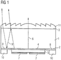
- FIG. 1 shows an embodiment of a semiconductor-based device with radiation-emitting properties according to the principle described above. It is as supporting element provided a transparent glass substrate 1. This glass substrate 1 has a first surface 2 and a second surface 3. On the first surface 2, a conversion layer 4 is applied, on which a semiconductor element 5 is accommodated. The semiconductor element 5 has radiation-emitting properties and is arranged on the conversion layer 4 such that the radiation direction 6 is directed through the conversion layer 4 and also through the glass substrate 1.
- the semiconductor element 5 is designed as a thin-film light-emitting diode and comprises at the surface facing away from the glass substrate 1 at least two electrically conductive contact surfaces 7 via which the semiconductor element 5 is supplied with electrical energy.
- the semiconductor element 5 does not cover the entire first surface 2 of the glass substrate 1 in the illustrated embodiment.
- the remaining regions of the first surface 2 of the glass substrate 1 are covered with a mirror 8.
- the mirror 8 causes scattered light components 9, which are returned by reflection in the direction of the first surface 2, to be guided on the mirror 8 likewise in the beam direction 6 and thus in the direction of the second surface 3.
- stray light loss is reduced.
- mounting base 10 At the outer edges of the first surface 2 mounting base 10 are formed, through which the semiconductor-based device can be stably fixed on a support substrate.
- the mounting sockets 10 are designed such that the entire semiconductor-based component is supported by the mounting sockets 10 at the installation site. Thus, mechanical stresses on the semiconductor element 5 are avoided.
- an optical element 11 is accommodated on the second surface 3 of the glass substrate 1.
- the embodiment shows the optical element 11 in the form of a Fresnel lens.
- a focused beam can be generated.
- the semiconductor-based device is not limited to this embodiment, but optical elements having other properties are usable, such as an optical diffuser. This is only dependent on the intended use of the semiconductor-based component.
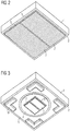
- the FIG. 2 shows the semiconductor-based device with radiation-emitting properties in a modification in which the semiconductor element 5 occupies almost the entire first surface 2 of the glass substrate 1.
- This embodiment is formed when the glass substrate 1 and its areal extent on the first surface 2, almost corresponds to the areal extent of the semiconductor element 5.
- the arrangement of mounting sockets 10 or the arrangement of a mirror 8 is not required.
- FIG. 3 shows the first embodiment of the semiconductor-based device in a perspective view.
- the viewing direction is directed to the first surface 2 of the semiconductor-based component.
- the semiconductor element 5, the conversion layer 4, the mirror 8 and the mounting base 10 are arranged. Centered on the first surface 2 of the glass substrate 1, following a circular shape, the conversion layer 4 is arranged, on which the semiconductor element 5 is preferred is arranged centrally.
- the semiconductor element 5 in turn has electrically conductive contact surfaces 7 which are provided at an installation location to supply the semiconductor element 5 with electrical energy.
- a mirror 8 is applied to reduce stray light losses.
- the glass substrate 1 is preferably designed in a square basic shape and comprises at least one mounting base 10 in each corner region of the first surface 2 of the glass substrate 1.
- the semiconductor-based component is fixed at an installation location.
- mechanical forces which act on the semiconductor-based component at an installation location are derived via the mounting base 10, so that the semiconductor element 5 is protected against mechanical stress.
- That in the FIG. 3 illustrated semiconductor-based component has a substantially square basic shape with an edge length of substantially 3 mm and a thickness of substantially 0.85 mm.
- the above described principle is not limited to these external dimensions. Rather, one of the advantages is the fact that the size of a single semiconductor-based device is determined according to the principle described above only by the requirements of the optical properties.
- FIG. 4 shows the first embodiment which also in the FIG. 1 and the FIG. 3 is shown in a perspective view.
- the viewing direction in this illustration is directed to the second surface 3 of the glass substrate 1.
- the optical element 11 is accommodated.
- the optical Element 11 executed according to a lens.
- the embodiment shows a Fresnel lens.
- FIG. 5 shows an embodiment of a carrier substrate for a semiconductor-based component according to the embodiments of the FIGS. 1 . 3 or 4 in which at least two electrically conductive contacts 13 are arranged on a printed circuit board 12. These contacts can be connected by means of feeding tracks with electrical signals or electrical energy.
- the semiconductor-based component and the carrier substrate are matched to one another, so that the electrical contact surfaces 7 of the semiconductor element 5 interact with the electrical contacts 13.
- On the carrier substrate socket receptacles 14 are arranged, which cooperate with the mounting bases 10 of the semiconductor-based component.
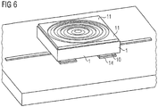
- the electrical contacts 13 are arranged centrally on the carrier substrate and are surrounded by base receptacles 14 such that each mounting base 10 can be received on a base receptacle 14 by a gluing process or a soldering process or other frictional methods.
- a semiconductor-based component arranged on the carrier substrate shows the FIG. 6 in a perspective view. There it is shown that each mounting base 10 is arranged on a respective base receptacle 14.
- FIGS. 7 to 12 describe in individual process steps a manufacturing method using the example of a single semiconductor-based device according to the above-described Principle and according to the first embodiment described above.
- a transparent glass substrate 1 having a square basic shape is shown. This already describes the shape which has a single semiconductor-based component.
- the lateral dimensions of the device are equal to the lateral dimensions of the glass substrate.
- An optimized production method for producing the semiconductor-based radiation-emitting components described above provides for processing a large number of such glass substrates simultaneously on a glass wafer.
- the glass wafer is then singulated in a predetermined substep of the manufacturing process, so that individual elements are formed.
- the process is shown by a single element.
- a conversion layer 4 is applied on the first surface 2 of the glass substrate 1, for example, on a portion of the first surface 2, a conversion layer 4 is applied.
- the conversion layer 4 is applied by means of a screen printing or stencil printing method.
- present is a uncovered by the mirror 8 middle region of the first surface 2 coated with the conversion layer 4.
- the mirror 8 is uncovered by the conversion layer 8 in the present case.
- FIG. 10 By means of - for example, photolithographically assisted - galvanic process, the application of the mounting base 10, respectively at the corner regions of the glass substrate 1.
- the mounting base 8 are applied, for example, on edge regions of the mirror 8.
- the second surface 3 is now provided with the optical element 10.
- the optical element 10 is introduced into an aging and temperature-stable layer, for example made of silicone.
- the in FIG. 12 illustrated step comprises applying the semiconductor element 5 to the conversion layer 4.
- the thin-film light-emitting diode is produced in a further production method and is arranged on the glass substrate 1 in the process step last described.
Landscapes
- Engineering & Computer Science (AREA)
- Microelectronics & Electronic Packaging (AREA)
- Manufacturing & Machinery (AREA)
- Computer Hardware Design (AREA)
- Power Engineering (AREA)
- Physics & Mathematics (AREA)
- Condensed Matter Physics & Semiconductors (AREA)
- General Physics & Mathematics (AREA)
- Led Device Packages (AREA)
Description
Die vorliegende Anmeldung betrifft ein halbleiterbasiertes Bauelement mit strahlungsemittierenden Eigenschaften, einTrägersubstrat für ein halbleiterbasiertes Bauelement und ein Verfahren zur Herstellung eines halbleiterbasierten Bauelements.The present application relates to a semiconductor-based device having radiation-emitting properties, a carrier substrate for a semiconductor-based device, and a method of manufacturing a semiconductor-based device.
In der Druckschrift
Die Druckschrift
Die Druckschrift
Halbleiterbasierte Bauelemente mit strahlungsemittierenden Eigenschaften, wie zum Beispiel Leuchtdioden, sind zumeist so gebildet, dass in ein Gehäuse aus einem Kunststoffmetallverbund oder in ein Gehäuse aus Keramik ein Halbleiterelement mit strahlungsemittierenden Eigenschaften montiert oder eingebettet ist. Während eines Produktionsprozesses eines derartigen halbleiterbasierten Bauelementes erfolgt die Montage des Halbleiterelements in dem Gehäuse mittels eines Lötvorgangs oder eines Klebeprozesses.Semiconductor-based components with radiation-emitting properties, such as light emitting diodes, are usually formed so that a semiconductor element with radiation-emitting properties is mounted or embedded in a housing made of a plastic metal composite or in a housing made of ceramic. During a production process of such a semiconductor-based component, the mounting of the semiconductor element in the housing takes place by means of a soldering process or an adhesive process.
Halbleiterelemente mit strahlungsemittierenden Eigenschaften wie zum Beispiel Dünnfilm-Leucht-Dioden können unterschieden werden in vertikal von Strom durchflossene Halbleiterelemente oder horizontal von Strom durchflossene Halbleiterelemente. Bei Halbleiterelementen, welche in vertikaler Richtung von Strom durchflossen sind, ist die Montagefläche des halbleiterbasierten Bauelements als ein einzelner elektrischer Kontakt ausgebildet. Ein zweiter elektrischer Kontakt ist auf der strahlungsemittierenden Seite des Halbleiterelementes angeordnet. Dieser Kontakt wird üblicherweise mit einem Bonddraht kontaktiert. Halbleiterelemente mit horizontalem Stromfluss sind derart ausgebildet, dass auf der Montagefläche des Halbleiterelementes zwei elektrische Kontakte ausgebildet sind.Semiconductor elements with radiation-emitting properties, such as, for example, thin-film light-emitting diodes, can be distinguished into semiconductor elements through which current flows, or semiconductor elements through which current flows. In semiconductor elements, which are traversed by current in the vertical direction, the mounting surface of the semiconductor-based Device formed as a single electrical contact. A second electrical contact is arranged on the radiation-emitting side of the semiconductor element. This contact is usually made with a bonding wire contacted. Semiconductor elements with horizontal current flow are formed such that two electrical contacts are formed on the mounting surface of the semiconductor element.
Insbesondere folgen bei einem vertikal von Strom durchflossenen Halbleiterelement der erste und der zweite elektrische Kontakt in Richtung einer Flächennormalen einer Haupterstreckungsebene des Halbleiterelements aufeinander. Bei einem horizontal von Strom durchflossenen Halbleiterelement sind der erste und der zweite elektrische Kontakt oder Bereiche des ersten und zweiten elektrischen Kontakts in Draufsicht auf die Haupterstreckungsebene nebeneinander angeordnet.In particular, in the case of a semiconductor element through which current flows, the first and second electrical contacts follow one another in the direction of a surface normal of a main extension plane of the semiconductor element. In a semiconductor element through which current flows, the first and second electrical contacts or regions of the first and second electrical contacts are arranged side by side in plan view on the main extension plane.
Zweckmäßigerweise ist der Stromfluss insbesondere nicht ausschließlich vertikal oder horizontal. Vielmehr findet bei vertikal stromdurchflossenen Halbleiterelementen vorzugweise eine laterale Stromaufweitung statt. Bei horizontal stromdurchflossenen Halbleiterelementen hat der Stromfluss innerhalb des Halbleiterelements insbesondere zumindest stellenweise eine zur Flächennormalen auf die Haupterstreckungsebene parallele Komponente.The current flow is expediently not exclusively vertical or horizontal. Rather, in the case of semiconductor elements which flow through vertically, it is preferable for lateral current spreading to take place. In the case of semiconductor elements with current flowing through them, the current flow within the semiconductor element has, in particular at least in places, a component parallel to the surface normal to the main extension plane.
Unabhängig von der Bauweise des Halbleiterelements selbst wird in dem Gehäuse durch Vergießen mit einem transparenten Harz oder einem anderen Einkapselungsmaterial das Halbleiterelement zusätzlich von äußeren Einflüssen geschützt. Eine statische Stabilität und ein Schutz vor mechanischer Belastung des Halbleiterelements erfolgt durch das Gehäuse, welches das Halbleiterelement schützend und tragend umgibt. Durch das ummantelnde Gehäuse ergibt sich für das Strahlungsemittierende halbleiterbasierte Bauelement eine Baugröße, welche die Größe des Halbleiterelementes selbst, weit überschreitet. Dies steht einer weiteren möglichen Miniaturisierung der Bauelemente entgegen.Regardless of the construction of the semiconductor element itself, the semiconductor element is additionally protected from external influences in the housing by casting with a transparent resin or other encapsulating material. Static stability and protection against mechanical loading of the semiconductor element is achieved by the housing, which surrounds the semiconductor element in a protective and load-bearing manner. The enclosing housing results in a size for the radiation-emitting semiconductor-based component which far exceeds the size of the semiconductor element itself. This is contrary to a further possible miniaturization of the components.
Es ist demzufolge die Aufgabe der Erfindung ein halbleiterbasiertes Bauelement mit strahlungsemittierenden Eigenschaften anzugeben, das eine weitere Miniaturisierung ermöglicht. Diese Aufgabe wird durch ein Bauelement und ein Verfahren gemäß den Ansprüchen 1 und 13 gelöst. Vorteilhafte Ausgestaltungen und Weiterbildungen sind in den jeweils abhängigen Patentansprüchen angegeben. Der Offenbarungsgehalt der Patentansprüche wird hiermit ausdrücklich durch Rückbezug in die Beschreibung aufgenommen.It is therefore the object of the invention to provide a semiconductor-based component with radiation-emitting properties, which enables further miniaturization. This object is achieved by a component and a method according to
Es wird ein halbleiterbasiertes Bauelement zur Montage auf einem Trägersubstrat angegeben. Das Bauelement umfasst ein Glassubstrat, welches eine erste Oberfläche und eine zweite Oberfläche, die der ersten Oberfläche gegenüber liegt, aufweist. Ein Halbleiterelement mit strahlungsemittierenden Eigenschaften ist auf der ersten Oberfläche angeordnet. Das Halbleiterelement weist zumindest zwei elektrisch leitende Kontaktflächen an der von der ersten Oberfläche des Glassubstrats abgewandten Seite auf. Eine Mehrzahl von galvanisch aufgebrachten Montagesockeln befindet sich auf dem Randbereich der ersten Oberfläche des Glassubstrats. Die Kontaktflächen sind so eingerichtet, dass sie durch Kleben mit einem leitfähigen Klebstoff oder durch Löten mit Kontakten des Trägersubstrats elektrisch leitend verbindbar sind. Die Montagesockel sind von den Kontaktflächen verschieden und weisen eine Materialstärke auf, welche der Gesamtdicke des Halbleiterelements gleicht, sodass die Montagesockel das Bauelement im unmontierten Zustand vor abrasiver Belastung schützen und im montierten Zustand mechanische Belastungen aufnehmen und an das Trägersubstrat ableiten können. Die Kontaktflächen liegen im unmontierten Zustand frei.A semiconductor-based component for mounting on a carrier substrate is specified. The device comprises a glass substrate having a first surface and a second surface opposite the first surface. A semiconductor element with radiation-emitting properties is arranged on the first surface. The semiconductor element has at least two electrically conductive contact surfaces on the side facing away from the first surface of the glass substrate. A plurality of galvanically mounted mounting sockets are located on the edge region of the first surface of the glass substrate. The contact surfaces are arranged so that they are electrically conductively connected by gluing with a conductive adhesive or by soldering to contacts of the carrier substrate. The mounting base are different from the contact surfaces and have a material thickness which is equal to the total thickness of the semiconductor element, so that the mounting base protect the component in the unassembled state from abrasive stress and absorb mechanical stresses in the assembled state and can derive to the carrier substrate. The contact surfaces are exposed in the unmounted state.
Das Glassubstrat weist im Wesentlichen zwei Oberflächen auf, die einander gegenüberliegend und insbesondere zueinander parallel angeordnet sind. Auf einer ersten Oberfläche des Glassubstrates ist ein Halbleiterelement angeordnet, welches strahlungsemittierende Eigenschaften aufweist. Das Halbleiterelement ist auf dieser Oberfläche so angeordnet, dass die Strahlungsrichtung zum Glassubstrat hin und weiter in dieses hinein gerichtet ist. Unter der Strahlungsrichtung wird vorliegend insbesondere eine zu einer Haupterstreckungsebene des Halbleiterelements senkrechte Richtung verstanden, in welche das Halbleiterelement im Betrieb elektromagnetische Strahlung emittiert. Vorteilhaft ist, dass das Glassubstrat ein tragendes Element für das Halbleiterelement bildet.The glass substrate has substantially two surfaces, which are arranged opposite one another and in particular parallel to one another. On a first surface of the glass substrate, a semiconductor element is arranged, which has radiation-emitting properties. The semiconductor element is arranged on this surface so that the radiation direction is directed towards the glass substrate and further into it. In the present case, the direction of radiation is understood to mean in particular a direction perpendicular to a main extension plane of the semiconductor element, into which the semiconductor element emits electromagnetic radiation during operation. It is advantageous that the glass substrate forms a supporting element for the semiconductor element.
Bei einer Ausgestaltung hat das halbleiterbasierte Bauelement eine im Wesentlichen quadratische Grundform. Bei einer Weiterbildung hat es eine Kantenlänge von im Wesentlichen 3 mm. Bei einer anderen Ausgestaltung hat es eine Dicke von im Wesentlichen 0,85 mm. Bei einer weiteren Ausgestaltung sind die lateralen Abmessungen des Bauelements gleich den lateralen Abmessungen des Glassubstrats.In one embodiment, the semiconductor-based component has a substantially square basic shape. In one development, it has an edge length of substantially 3 mm. In another embodiment, it has a thickness of substantially 0.85 mm. In a further embodiment, the lateral dimensions of the component are equal to the lateral dimensions of the glass substrate.
Bei einer Ausgestaltung ist das Halbleiterelement als Dünnfilm-Leuchtdiode ausgebildet. Für Halbleiterelemente mit horizontalem Stromfluss, insbesondere für Dünnfilm-Leucht-Dioden, bildet das Glassubstrat als tragendes Element einen wesentlichen Vorteil, da im besonderen bei Dünnfilm-Leucht-Dioden während des Produktionsprozesses ein Aufwachssubstrat abgetrennt wird. Dieses Aufwachssubstrat bildet während des Produktionsprozesses das tragende Element für diese Halbleiterelemente. Durch das Abtrennen des Aufwachssubstrates während des Produktionsprozesses sind alternative Elemente erforderlich, welche tragende Eigenschaften aufweisen. Das Glassubstrat bietet nicht nur tragende Eigenschaften, sondern schützt das Halbleiterelement vor mechanischer Belastung. Ein Grundprinzip einer Dünnfilm-Leucht-Diode ist beispielsweise in der Druckschrift I.
Bei einer anderen Ausgestaltung ist an einer von dem Glassubstrat abgewandten Hauptfläche einer strahlungserzeugenden Halbleiterschichtenfolge der Dünnfilm-Leuchtdiode, bei der es sich insbesondere um eine strahlungserzeugende Epitaxie-Schichtenfolge handelt, eine reflektierende Schicht aufgebracht oder ausgebildet, die zumindest einen Teil der in der Halbleiterschichtenfolge erzeugten elektromagnetischen Strahlung in diese zurück und in Richtung des Glassubstrats reflektiert.In another embodiment, a reflective layer is applied or formed on a main surface facing away from the glass substrate of a radiation-generating semiconductor layer sequence of the thin-film light emitting diode, which is in particular a radiation-generating epitaxial layer sequence, the at least a portion of the electromagnetic generated in the semiconductor layer sequence Radiation in this back and reflected in the direction of the glass substrate.
Eine dem Glassubstrat zugewandte Hauptfläche des Halbleiterelements ist bei einer Ausgestaltung des Bauelements frei von elektrischen Anschlussflächen, auch Kontakte oder Kontaktflächen genannt. Zwei elektrische Anschlussflächen, die zur n-seitigen und zur p-seitigen Kontaktierung des Halbleiterelements vorgesehen sind, sind an einer von dem Glassubstrat abgewandten Seite des Halbleiterelements angeordnet.A glass substrate facing the main surface of the semiconductor element is in an embodiment of the device free of electrical pads, also called contacts or contact surfaces. Two electrical connection surfaces, which are provided for n-side and p-side contacting of the semiconductor element, are arranged on a side of the semiconductor element facing away from the glass substrate.
Gemäß einer Weiterbildung des strahlungsemittierenden halbleiterbasierten Bauelements ist vorgesehen, auf der zweiten Oberfläche des Glassubstrates ein optisches Element anzuordnen. Somit werden die emittierten Strahlen des Halbleiterelements durch das Glassubstrat hindurch und ebenfalls durch das optische Element hindurch emittiert. Mit dem optischen Element lassen sich, je nach Verwendungszweck des strahlungsemittierenden halbleiterbasierten Bauelements und abhängig von den optischen Eigenschaften des optischen Elements verschiedene Wirkungen erzielen. Mit einem optischen Element, zum Beispiel ausgebildet als eine Linse, lässt sich ein gebündelter Strahl bilden. Mit einem optischen Element, ausgebildet als optischer Diffusor lässt sich die emittierte Strahlung streuen. Abhängig von der jeweiligen Verwendung des halbleiterbasierten Bauelementes lassen sich so verschiedene Eigenschaften ausbilden. Ein derart ausgebildetes strahlungsemittierendes halbleiterbasiertes Bauelement ist in Bezug auf dessen Größe frei skalierbar. Die erforderlichen Breiten- und Höhemaße orientieren sich im Wesentlichen an den gewünschten optischen Eigenschaften.According to a development of the radiation-emitting semiconductor-based component, it is provided to arrange an optical element on the second surface of the glass substrate. Thus, the emitted rays of the semiconductor element are emitted through the glass substrate and also through the optical element. Depending on the intended use of the radiation-emitting semiconductor-based component and on the optical properties of the optical element, various effects can be achieved with the optical element. With an optical element, for example formed as a lens, can be a bundled Forming a jet. With an optical element, designed as an optical diffuser, the emitted radiation can be scattered. Depending on the particular use of the semiconductor-based component so different properties can be formed. A radiation-emitting semiconductor-based component designed in this way is freely scalable with regard to its size. The required width and height dimensions are essentially based on the desired optical properties.
Zur Erzeugung von vorbestimmten Lichtfarben, beziehungsweise von vorbestimmten Wellenlängen der durch das halbleiterbasierte Bauelement emittierten Strahlung und insbesondere von mischfarbigem Licht, ist gemäß einer Weiterbildung des halbleiterbasierten Bauelements, zwischen dem strahlungsemittierenden Halbleiterelement und der ersten Oberfläche des Glassubstrates eine Konversionsschicht angeordnet. Eine Konversionsschicht wandelt die Wellenlänge der durch sie hindurch tretenden Strahlen zumindest für einen Teil der Strahlen. So lassen sich Farbtöne bilden die alleine durch die Strahlungsemission des Halbleiterelements nicht erzeugbar sind. So lässt sich zum Beispiel auf einfache und kostengünstige Weise weißes Licht erzeugen, indem ein Halbleiterelement welches blaues Licht emittiert, mit einer gelben Konversionsschicht kombiniert wird.For generating predetermined light colors, or of predetermined wavelengths of the radiation emitted by the semiconductor-based component and in particular mixed-colored light, a conversion layer is arranged between the radiation-emitting semiconductor element and the first surface of the glass substrate according to a development of the semiconductor-based component. A conversion layer converts the wavelength of the rays passing through it, at least for a part of the rays. This makes it possible to form hues which can not be generated solely by the radiation emission of the semiconductor element. For example, white light can be generated in a simple and inexpensive manner by combining a semiconductor element which emits blue light with a yellow conversion layer.
Es ist vorgesehen, das Glassubstrat bezogen auf dessen erste Oberfläche größer auszubilden als dies zur Aufnahme des Halbleiterelementes erforderlich wäre und dabei zusätzlich mehrere Montagesockel vorzusehen. Jeder der Montagesockel weist eine Materialstärke auf, welche der Gesamtdicke des Halbleiterelements gleicht und ist ausgebildet, mechanische Belastungen, welche auf das Glassubstrat beziehungsweise auf das halbleiterbasierte Bauelement wirken, aufzunehmen und an den Montageort abzuleiten. Damit ist, in einem eingebauten Zustand, das Halbleiterelement von mechanischen Belastungen rundum geschützt. Ein weiterer Vorteil dieser Anordnung ist dadurch gegeben, dass auch in einem nicht eingebauten Zustand, das Halbleiterelement vor abrasiven Belastungen etwas geschützt ist.It is envisaged that the glass substrate be made larger with respect to its first surface than would be required to accommodate the semiconductor element and additionally provide several mounting sockets. Each of the mounting base has a material thickness which is equal to the total thickness of the semiconductor element and is designed to mechanical loads, which on the glass substrate or on the Semiconductor-based device act to absorb and dissipate to the mounting location. Thus, in a built-in state, the semiconductor element is completely protected from mechanical stresses. Another advantage of this arrangement is given by the fact that even in a non-installed state, the semiconductor element is somewhat protected from abrasive loads.
Gemäß einer Weiterbildung des halbleiterbasierten Bauelements mit strahlungsemittierenden Eigenschaften ist vorgesehen, zur Vermeidung von Streulichtverlusten die von dem Halbleiterelement nicht bedeckten Flächen durch einen Spiegel zu bedecken. Dieser ist bei einer Ausgestaltung direkt auf der ersten Oberfläche des Glassubstrates aufgebracht und bedeckt lediglich die von dem Halbleiterelement nicht bedecken Bereiche der ersten Oberfläche. Somit sind, von fertigungstechnisch bedingten Ausnahmen abgesehen, auf dem Glassubstrat entweder strahlungsemittierende Flächen, oder strahlungsreflektierende Flächen ausgebildet. Wobei die strahlungsemittierenden Flächen durch das Halbleiterelement gebildet sind und die strahlungsreflektierenden Flächen, durch den Spiegel gebildet sind.According to a development of the semiconductor-based component with radiation-emitting properties, it is provided to cover the surfaces not covered by the semiconductor element by a mirror in order to avoid stray light losses. This is applied in one embodiment directly on the first surface of the glass substrate and covers only the not covered by the semiconductor element regions of the first surface. Thus, apart from production-related exceptions, formed on the glass substrate either radiation-emitting surfaces, or radiation-reflecting surfaces. Wherein the radiation-emitting surfaces are formed by the semiconductor element and the radiation-reflecting surfaces are formed by the mirror.
Weiter wird ein Trägersubstrat angegeben, das vorgesehen ist, das halbleiterbasierte Bauelement aufzunehmen, welches gemäß dem vorstehend beschriebenen Prinzip ausgebildet ist.Furthermore, a carrier substrate is provided, which is provided to receive the semiconductor-based component, which is designed according to the principle described above.
Das Trägersubstrat weist dabei zwei elektrische Kontakte auf, die beschaltbar ausgeführt sind. Somit sind elektrische Signale beziehungsweise ist elektrische Energie einem von dem Trägersubstrat aufgenommenen halbleiterbasiertem Bauelement zuführbar. In Größe und flächiger Ausbildung sind die elektrischen Kontakte bei einer Ausgestaltung gleich den Kontaktelementen des Halbleiterelementes ausgeführt. So ist durch Kleben mit einem leitfähigen Klebstoff, oder durch Löten, ein elektrischer Kontakt zwischen dem Halbleiterelement und dem Trägersubstrat herstellbar. Die Kontaktelemente sind umgeben mit zumindest einer Sockelaufnahme, auf der der zumindest eine Montagesockel aufnehmbar ist. Die Sockelaufnahme ist elektrisch neutral und bildet demzufolge keine elektrische Verbindung mit den elektrischen Kontakten.The carrier substrate has two electrical contacts, which are designed to be connected. Thus, electrical signals or electrical energy can be fed to a semiconductor-based component accommodated by the carrier substrate. In size and planar design, the electrical contacts in one embodiment are equal to the contact elements of the semiconductor element. Thus, by bonding with a conductive adhesive, or by soldering, an electrical contact between the semiconductor element and the carrier substrate can be produced. The contact elements are surrounded with at least one base receptacle on which the at least one mounting base is receivable. The base receptacle is electrically neutral and therefore forms no electrical connection with the electrical contacts.
Weiter wird ein Verfahren zur Herstellung eines halbleiterbasierten Bauelementes angegeben. Das Verfahren umfasst die folgenden Schritte.Furthermore, a method for producing a semiconductor-based component is specified. The method comprises the following steps.
Ein Schritt umfasst ein Bereitstellen eines Glassubstrats. Ein drauffolgender zweiter Schritt umfasst das Aufbringen eines Halbleiterelementes auf einer ersten Oberfläche und das Aufbringen eines optischen Elementes auf einer zweiten Oberfläche des Glassubstrats.One step involves providing a glass substrate. A subsequent second step comprises applying a semiconductor element on a first surface and applying an optical element on a second surface of the glass substrate.
Das Verfahren lässt sich auf eine Vielzahl von Glassubstraten gleichzeitig anwenden, wobei ein Glaswafer vorgesehen ist, auf dem parallel eine Vielzahl von Halbleiterbasierten Bauelementen gebildet wird. Ein Verfahrensschritt umfasst dann das Vereinzeln der halbleiterbasierten Bauelemente des gesamten Glaswafers.The method can be applied simultaneously to a plurality of glass substrates, wherein a glass wafer is provided, on which a plurality of semiconductor-based components is formed in parallel. A method step then comprises the singulation of the semiconductor-based components of the entire glass wafer.
Eine Weiterbildung des Verfahrens sieht vor, ein halbleiterbasiertes Bauelement mit strahlungsemittierenden Eigenschaften herzustellen, welches Strahlung einer vorbestimmten Wellenlänge oder mischfarbiges Licht, wie zum Beispiel weißes Licht, emittiert. Beispielsweise um Wellenlängen zu erzeugen, welche mittels bekannter Halbleiterwerkstoffe alleine nicht erzeugbar sind, wird gemäß einer Weiterbildung vor dem Aufbringen des Halbleiterelementes eine Konversionsschicht auf die erste Oberfläche des Glassubstrats aufgebracht. Dabei findet bevorzugt ein Siebdruckverfahren oder ein Schablonendruckverfahren Anwendung.A development of the method provides for producing a semiconductor-based component with radiation-emitting properties, which emits radiation of a predetermined wavelength or mixed-colored light, such as white light. For example, in order to generate wavelengths which can not be generated by known semiconductor materials alone, according to a development before the application of the semiconductor element, a conversion layer is applied to the first surface of the glass substrate. In this case, a screen printing method or a stencil printing method is preferably used.
Für ein Halbleiterelement, dessen flächige Ausdehnung kleiner ist als die erste Oberfläche des Glassubstrats, ist vorgesehen eine Spiegelschicht aufzubringen, die mittels eines fototechnisch beeinflussten Sputter- oder Bedampfverfahren aufgebracht wird. Dabei wird die erste Oberfläche des Glassubstrats fototechnisch, insbesondere mittels eine fotolithografischen Prozesses, vorbehandelt, so dass lediglich die Bereiche mittels des Sputter- oder Bedampfverfahrens behandelbar sind, welche von dem Halbleiterelement und einer eventuell aufzubringenden Konversionsschicht unbedeckt bleiben.For a semiconductor element, the areal extent of which is smaller than the first surface of the glass substrate, it is provided to apply a mirror layer, which is applied by means of a photo-technically influenced sputtering or vapor deposition method. In this case, the first surface of the glass substrate is phototechnically pretreated, in particular by means of a photolithographic process, so that only the areas can be treated by means of the sputtering or vapor deposition process, which remain uncovered by the semiconductor element and any conversion layer to be applied.
Auf der zweiten Oberfläche des Glassubstrats wird das optische Element in eine alterungs- und temperaturstabile Schicht, bevorzugt aus Silikon eingebracht.On the second surface of the glass substrate, the optical element is introduced into an aging and temperature-stable layer, preferably made of silicone.
Nachfolgend wird die Erfindung anhand zweier Ausführungsbeispiele und unter Zuhilfenahme von 12 Figuren näher erläutert.The invention will be explained in more detail with reference to two embodiments and with the aid of 12 figures.
Es zeigt die
Figur 1- das halbleiterbasierte Bauelement in einer ersten Ausführungsform in einer schematischen Querschnittsdarstellung,
Figur 2- das halbleiterbasierte Bauelement in einer Abwandlung in schematischer perspektivischer Darstellung,
Figur 3- das halbleiterbasierte Bauelement der ersten Ausführungsform in schematischer perspektivischer Darstellung,
Figur 4- das halbleiterbasierte Bauelement der ersten Ausführungsform in schematischer perspektivischer Darstellung,
- Figur 5
- einen Ausschnitt eines Trägersubstrats für das halbleiterbasierte Bauelement gemäß der ersten Ausführungsform in einer schematischen perspektivischen Darstellung,
Figur 6- das halbleiterbasierte Bauelement gemäß der ersten Ausführungsform auf dem Trägersubstrat in einer schematischen perspektivischen Darstellung, und
- Figuren
- 7
bis 12 schematische perspektivische Darstellungen einzelner Verfahrensschritte eines Ausführungsbeispiels eines Verfahrens zur Herstellung des halbleiterbasierten Bauelement der ersten Ausführungsform.
- FIG. 1
- the semiconductor-based component in a first embodiment in a schematic cross-sectional representation,
- FIG. 2
- the semiconductor-based component in a modification in a schematic perspective view,
- FIG. 3
- the semiconductor-based component of the first embodiment in a schematic perspective view,
- FIG. 4
- the semiconductor-based component of the first embodiment in a schematic perspective view,
- FIG. 5
- a section of a carrier substrate for the semiconductor-based component according to the first embodiment in a schematic perspective view,
- FIG. 6
- the semiconductor-based device according to the first embodiment on the carrier substrate in a schematic perspective view, and
- characters
- FIGS. 7 to 12 show schematic perspective illustrations of individual method steps of an exemplary embodiment of a method for producing the semiconductor-based component of the first embodiment.
Figurübergreifend werden Elemente mit gleichen Funktionen mit gleichen Bezugszeichen versehen. Die Figuren und die Größenverhältnisse der in den Figuren dargestellten Elemente untereinander sind nicht als maßstäblich zu betrachten. Vielmehr können einzelne Elemente zur besseren Darstellbarkeit und/oder zum besseren Verständnis übertrieben groß dargestellt sein.Cross-figure elements with the same functions are given the same reference numbers. The figures and the proportions of the elements shown in the figures with each other are not to be considered to scale. Rather, individual elements may be exaggerated in size for better representability and / or better understanding.
Bevorzugt ist das Halbleiterelement 5 als Dünnfilm-Leucht-Diode ausgeführt und umfasst an der vom Glassubstrat 1 abgewandten Oberfläche zumindest zwei elektrisch leitende Kontaktflächen 7 über die das Halbleiterelement 5 mit elektrischer Energie versorgt wird. Das Halbleiterelement 5 bedeckt bei dem dargestellten Ausführungsbeispiel nicht die gesamte erste Oberfläche 2 des Glassubstrates 1. Die verbleibenden Bereiche der ersten Oberfläche 2 des Glassubstrates 1 sind mit einem Spiegel 8 bedeckt. Der Spiegel 8 bewirkt, dass Streulichtanteile 9, welche durch Reflektion in Richtung der ersten Oberfläche 2 zurückgeleitet werden, an dem Spiegel 8 ebenso wieder in die Strahlrichtung 6 und damit in Richtung der zweiten Oberfläche 3 geleitet werden. Somit ist Streulichtverlust vermindert.Preferably, the semiconductor element 5 is designed as a thin-film light-emitting diode and comprises at the surface facing away from the
An den äußeren Rändern der ersten Oberfläche 2 sind Montagesockel 10 ausgebildet, durch welche das halbleiterbasierte Bauelement auf einem Trägersubstrat stabil festgelegt werden kann. Die Montagesockel 10 sind dergestalt ausgeführt, dass das gesamte halbleiterbasierte Bauelement durch die Montagesockel 10 an dem Einbauort getragen ist. So sind mechanische Belastungen am Halbleiterelement 5 vermieden.At the outer edges of the
Auf der zweiten Oberfläche 3 des Glassubstrats 1 ist ein optisches Element 11 aufgenommen. Das Ausführungsbeispiel zeigt das optische Element 11 in Form einer Fresnellinse. Mittels des optischen Elements 11 in Form einer Fresnellinse ist ein gebündelter Strahl erzeugbar. Das halbleiterbasierte Bauelement ist aber nicht auf dieses Ausführungsbeispiel begrenzt, vielmehr sind optische Elemente mit anderen Eigenschaften verwendbar, wie zum Beispiel ein optischer Diffusor. Dies ist lediglich abhängig von dem Verwendungszweck des halbleiterbasierten Bauelements.On the
Die
Die
Auf dieser Oberfläche sind das Halbleiterelement 5, die Konversionsschicht 4, der Spiegel 8 und die Montagesockel 10 angeordnet. Mittig auf der ersten Oberfläche 2 des Glassubstrats 1 ist einer kreisrunden Form folgend, die Konversionsschicht 4 angeordnet, auf welcher das Halbleiterelement 5 bevorzugt mittig angeordnet ist. Das Halbleiterelement 5 weist seinerseits elektrisch leitende Kontaktflächen 7 auf, die vorgesehen sind an einem Einbauort das Halbleiterelement 5 mit elektrischer Energie zu versorgen. Die kreisrunde Konversionsschicht 4 umgebend, ist ein Spiegel 8 aufgebracht, zur Verminderung von Streulichtverlusten.On this surface, the semiconductor element 5, the
Das Glassubstrat 1 ist bevorzugt in einer quadratischen Grundform ausgeführt und umfasst zumindest einem Montagesockel 10 in jedem Eckbereich der ersten Oberfläche 2 des Glassubstrats 1. Mittels der Montagesockel 10 wird das halbleiterbasierte Bauelement an einem Einbauort fixiert. Dabei werden mechanische Kräfte, die auf das halbleiterbasierte Bauelement an einem Einbauort wirken über die Montagesockel 10 abgeleitet, so dass das Halbleiterelement 5 vor mechanischer Belastung geschützt ist. Das in der
Die
Ein auf dem Trägersubstrat angeordnetes halbleiterbasiertes Bauelement zeigt die
Die
In
Ein optimiertes Produktionsverfahren zur Herstellung vorstehend beschriebener halbleiterbasierter strahlungsemittierender Bauelemente sieht vor, eine Vielzahl von solchen Glassubstraten gleichzeitig auf einem Glaswafer zu bearbeiten. Der Glaswafer wird dann in einem vorbestimmten Teilschritt des Herstellungsverfahrens vereinzelt, so dass einzelne Elemente gebildet sind. Zum besseren Verständnis des Herstellungsverfahrens ist das Verfahren anhand eines einzelnen Elements gezeigt.An optimized production method for producing the semiconductor-based radiation-emitting components described above provides for processing a large number of such glass substrates simultaneously on a glass wafer. The glass wafer is then singulated in a predetermined substep of the manufacturing process, so that individual elements are formed. For a better understanding of the manufacturing process, the process is shown by a single element.
Ausgehend von dem Glassubstrat 1 wird, dargestellt in
Anschließend wird, gezeigt in
Anschließend erfolgt, gezeigt in
In einem nachfolgenden Verfahrensschritt, dargestellt in Figur 11, wird nunmehr die zweite Oberfläche 3 mit dem optischen Element 10 versehen. Das optische Element 10 wird dabei in eine alterungs- und temperaturstabile Schicht zum Beispiel aus Silikon eingebracht.In a subsequent method step, illustrated in FIG. 11, the
Der in
Claims (13)
- Semiconductor based component for mounting on a carrier substrate, comprising- a glass substrate (1), which comprises a first surface (2) and a second surface (3), which lies opposite the first surface (2),- a semiconductor element (5) with radiation-emitting properties, which is arranged on the first surface (2), wherein the semiconductor element (5) comprises at least two electrically conductive contact areas (7) on the side facing away from the first surface (2) of the glass substrate (1),- a plurality of electroplated mounting bases (10) on the peripheral area of the first surface (2) of the glass substrate (1),wherein- the contact surfaces (7) are configured such that they are electrically-conductively connectable by bonding with a conductive adhesive or by soldering with contacts of the carrier substrate,- the mounting bases (10) are distinct from the contact surfaces (7) and have a material thickness which equals the total thickness of the semiconductor element (5), so that the mounting bases (10) protect the component from abrasive stress in the unmounted state, and can absorb mechanical stresses in the mounted state and can divert them to the carrier substrate,- the contact surfaces (7) are exposed in the unmounted state.
- Semiconductor based component according to claim 1,
characterized in that
on the second surface (3), an optical element (11) is received. - Semiconductor based component according to one of the claims 1 or 2,
characterized in that
between the first surface (2) and the radiation-emitting semiconductor element (5), a conversion layer (4) is arranged. - Semiconductor based component according to at least claim 2,
characterized in that the optical element comprises the form of a Fresnel lens,
or in that the optical element (11) is formed as optical diffuser. - Semiconductor based component according to one of the preceding claims,
characterized in that
not the entire first surface (2) is covered by the semiconductor element (5), and in that remaining areas of the first surface (2) are covered by a mirror (8). - Semiconductor based component according to the claims 3 and 5,
characterized in that
a central area of the first surface (2) not covered by the mirror (8) is coated with the conversion layer (4), wherein the conversion layer (4) is not covered by the mirror (8). - Semiconductor based component according to the preceding claim,
characterized in that
the conversion layer (4) is circular in shape, and the transparent glass substrate (1) has a square base shape. - Semiconductor based component according to the preceding claim,
characterized in that
the semiconductor element (5) is arranged centrally on the first surface (2) and surrounded by the mounting bases (10). - Semiconductor based component according to one of the preceding claims,
characterized in that
the glass substrate (1) is a load-bearing element of the semiconductor based component. - Semiconductor based component according to one of the preceding claims,
characterized in that
the semiconductor element (5) is a thin-film light-emitting diode, which, without the glass substrate (1), has a thickness of 20 µm or less. - Semiconductor based component according to the preceding claim,
characterized in that
a reflective layer is applied or formed on a main surface of the semiconductor element (5) facing away from the glass substrate (1), which reflects at least a part of the electromagnetic radiation generated in the semiconductor element (5) back therein and in direction of the glass substrate (1). - Semiconductor based component according to at least claim 2,
characterized in that
the optical element (10) is incorporated in an age-resistant and temperature-stable layer of silicone. - Method for producing a semiconductor based component according to one of the preceding claims, comprising the following steps:- providing a glass substrate (1),- applying a semiconductor element (5) on a first surface (2) of the glass substrate (1).
Applications Claiming Priority (3)
| Application Number | Priority Date | Filing Date | Title |
|---|---|---|---|
| DE102007046744 | 2007-09-28 | ||
| DE102008005345A DE102008005345A1 (en) | 2007-09-28 | 2008-01-21 | Semiconductor-based device, semiconductor device-based device receptacle, and method of making a semiconductor-based device |
| PCT/DE2008/001533 WO2009039829A1 (en) | 2007-09-28 | 2008-09-12 | Radiation-emitting semi-conductor component, receptacle for a radiation-emitting semiconductor component, and method for producing a radiation-emitting semiconductor component |
Publications (2)
| Publication Number | Publication Date |
|---|---|
| EP2195865A1 EP2195865A1 (en) | 2010-06-16 |
| EP2195865B1 true EP2195865B1 (en) | 2018-03-14 |
Family
ID=40384495
Family Applications (1)
| Application Number | Title | Priority Date | Filing Date |
|---|---|---|---|
| EP08801325.5A Not-in-force EP2195865B1 (en) | 2007-09-28 | 2008-09-12 | Radiation-emitting semi-conductor component and method for producing a radiation-emitting semiconductor component |
Country Status (8)
| Country | Link |
|---|---|
| US (1) | US8878195B2 (en) |
| EP (1) | EP2195865B1 (en) |
| JP (1) | JP5295250B2 (en) |
| KR (1) | KR101515252B1 (en) |
| CN (1) | CN101809774B (en) |
| DE (1) | DE102008005345A1 (en) |
| TW (1) | TW200921953A (en) |
| WO (1) | WO2009039829A1 (en) |
Families Citing this family (3)
| Publication number | Priority date | Publication date | Assignee | Title |
|---|---|---|---|---|
| US9270427B2 (en) | 2010-01-11 | 2016-02-23 | Futurewei Technologies, Inc. | System and method for multiplexing control and data channels in a multiple input, multiple output communications system |
| DE102011077898A1 (en) * | 2011-06-21 | 2012-12-27 | Osram Ag | LED lighting device and method for producing an LED lighting device |
| JP6848245B2 (en) * | 2016-07-27 | 2021-03-24 | 日亜化学工業株式会社 | Light emitting device |
Citations (5)
| Publication number | Priority date | Publication date | Assignee | Title |
|---|---|---|---|---|
| EP1267420A2 (en) * | 2001-06-12 | 2002-12-18 | LumiLeds Lighting U.S., LLC | Light emitting diodes with improved light extraction efficiency |
| DE10308890A1 (en) * | 2003-02-28 | 2004-09-09 | Opto Tech Corporation | A housing structure with a substrate, two electrodes, and a transparent insulated carrier with a depression useful for light emitting diodes |
| EP1603170A1 (en) * | 2003-03-10 | 2005-12-07 | Toyoda Gosei Co., Ltd. | Solid element device and method for manufacture thereof |
| US20070064131A1 (en) * | 2005-09-13 | 2007-03-22 | Sumita Optical Glass, Inc. | Solid-state element device and light-emitting apparatus using same |
| EP2666745A1 (en) * | 2007-06-20 | 2013-11-27 | Shinko Electric Industries Co., Ltd. | Electronic component package and method of manufacturing the same, and electronic component device |
Family Cites Families (22)
| Publication number | Priority date | Publication date | Assignee | Title |
|---|---|---|---|---|
| DE3470441D1 (en) * | 1983-12-22 | 1988-05-19 | Sumitomo Chemical Co | Film-forming composition comprising indium and tin compounds |
| US4837927A (en) | 1985-04-22 | 1989-06-13 | Savage John Jun | Method of mounting circuit component to a circuit board |
| JPS63262259A (en) * | 1987-04-20 | 1988-10-28 | Matsushita Electric Ind Co Ltd | Writing head for optical printer |
| US4942405A (en) * | 1988-10-11 | 1990-07-17 | Hewlett-Packard Company | Light emitting diode print head assembly |
| JPH04159519A (en) * | 1990-10-24 | 1992-06-02 | Stanley Electric Co Ltd | Liquid crystal display device with led backlight and its manufacture |
| JP3460330B2 (en) * | 1994-08-31 | 2003-10-27 | 京セラ株式会社 | Imaging device |
| DE19527026C2 (en) | 1995-07-24 | 1997-12-18 | Siemens Ag | Optoelectronic converter and manufacturing process |
| DE19600306C1 (en) * | 1996-01-05 | 1997-04-10 | Siemens Ag | Semiconductor component with hermetically-sealed housing for opto-electronic component |
| DE19746893B4 (en) * | 1997-10-23 | 2005-09-01 | Siemens Ag | Optoelectronic component with heat sink in the base part and method for the production |
| JP4109756B2 (en) | 1998-07-07 | 2008-07-02 | スタンレー電気株式会社 | Light emitting diode |
| JP2000135814A (en) | 1998-10-30 | 2000-05-16 | Kyocera Corp | Optical printer head |
| US6396082B1 (en) * | 1999-07-29 | 2002-05-28 | Citizen Electronics Co., Ltd. | Light-emitting diode |
| JP2001077430A (en) | 1999-09-02 | 2001-03-23 | Citizen Electronics Co Ltd | Light-emitting diode |
| JP3652945B2 (en) * | 1999-12-28 | 2005-05-25 | 松下電器産業株式会社 | Optical information processing equipment |
| JP4401681B2 (en) | 2003-05-19 | 2010-01-20 | 日東樹脂工業株式会社 | Light diffuser and optical member or optical device using the same |
| JP2005072129A (en) | 2003-08-21 | 2005-03-17 | Nec Lighting Ltd | Visible light emitting device, its manufacturing method, and display |
| JP4843235B2 (en) * | 2004-03-18 | 2011-12-21 | 昭和電工株式会社 | Group III nitride semiconductor light emitting device manufacturing method |
| WO2006117710A1 (en) | 2005-04-29 | 2006-11-09 | Koninklijke Philips Electronics N.V. | Light source with glass housing |
| TWM285801U (en) | 2005-08-03 | 2006-01-11 | Lighthouse Technology Co Ltd | Light-emitting diode package structure |
| US7329907B2 (en) * | 2005-08-12 | 2008-02-12 | Avago Technologies, Ecbu Ip Pte Ltd | Phosphor-converted LED devices having improved light distribution uniformity |
| JP4759357B2 (en) * | 2005-09-28 | 2011-08-31 | 日立アプライアンス株式会社 | LED light source module |
| US20070228386A1 (en) * | 2006-03-30 | 2007-10-04 | Jin-Shown Shie | Wire-bonding free packaging structure of light emitted diode |
-
2008
- 2008-01-21 DE DE102008005345A patent/DE102008005345A1/en not_active Withdrawn
- 2008-09-12 KR KR1020107009389A patent/KR101515252B1/en active IP Right Grant
- 2008-09-12 WO PCT/DE2008/001533 patent/WO2009039829A1/en active Application Filing
- 2008-09-12 EP EP08801325.5A patent/EP2195865B1/en not_active Not-in-force
- 2008-09-12 US US12/680,674 patent/US8878195B2/en not_active Expired - Fee Related
- 2008-09-12 CN CN2008801096470A patent/CN101809774B/en not_active Expired - Fee Related
- 2008-09-12 JP JP2010526157A patent/JP5295250B2/en not_active Expired - Fee Related
- 2008-09-22 TW TW097136254A patent/TW200921953A/en unknown
Patent Citations (5)
| Publication number | Priority date | Publication date | Assignee | Title |
|---|---|---|---|---|
| EP1267420A2 (en) * | 2001-06-12 | 2002-12-18 | LumiLeds Lighting U.S., LLC | Light emitting diodes with improved light extraction efficiency |
| DE10308890A1 (en) * | 2003-02-28 | 2004-09-09 | Opto Tech Corporation | A housing structure with a substrate, two electrodes, and a transparent insulated carrier with a depression useful for light emitting diodes |
| EP1603170A1 (en) * | 2003-03-10 | 2005-12-07 | Toyoda Gosei Co., Ltd. | Solid element device and method for manufacture thereof |
| US20070064131A1 (en) * | 2005-09-13 | 2007-03-22 | Sumita Optical Glass, Inc. | Solid-state element device and light-emitting apparatus using same |
| EP2666745A1 (en) * | 2007-06-20 | 2013-11-27 | Shinko Electric Industries Co., Ltd. | Electronic component package and method of manufacturing the same, and electronic component device |
Also Published As
| Publication number | Publication date |
|---|---|
| JP5295250B2 (en) | 2013-09-18 |
| KR20100063139A (en) | 2010-06-10 |
| JP2010541222A (en) | 2010-12-24 |
| KR101515252B1 (en) | 2015-04-24 |
| US8878195B2 (en) | 2014-11-04 |
| CN101809774B (en) | 2012-08-29 |
| DE102008005345A1 (en) | 2009-04-02 |
| WO2009039829A1 (en) | 2009-04-02 |
| CN101809774A (en) | 2010-08-18 |
| EP2195865A1 (en) | 2010-06-16 |
| TW200921953A (en) | 2009-05-16 |
| US20110057218A1 (en) | 2011-03-10 |
Similar Documents
| Publication | Publication Date | Title |
|---|---|---|
| DE102008025756B4 (en) | semiconductor device | |
| DE102010028407B4 (en) | Optoelectronic component and method for producing an optoelectronic component | |
| DE102008021402B4 (en) | Surface mount light emitting diode module and method for manufacturing a surface mount light emitting diode module | |
| EP2258000B1 (en) | Optoelectronic semiconductor component and method for producing said component | |
| DE102012002605B4 (en) | Method for producing an optoelectronic semiconductor component and optoelectronic semiconductor component | |
| DE102013101262A1 (en) | Optoelectronic light module, optoelectronic light device and vehicle headlights | |
| DE102011116534B4 (en) | Radiation-emitting component | |
| WO2020169524A1 (en) | Optoelectronic semiconductor component, and method for producing optoelectronic semiconductor components | |
| EP1312124A1 (en) | Optoelectronic component and method for the production thereof, module and device comprising a module of this type | |
| DE102013212928A1 (en) | Method for producing an optoelectronic component | |
| DE102008010512A1 (en) | Optoelectronic component, particularly light emitting diode or photodiode, has semiconductor chip with chip lower side, and two electrical bondings with contact lower sides | |
| DE112015005127B4 (en) | Optoelectronic semiconductor component and method for producing an optoelectronic semiconductor component | |
| DE102005034166A1 (en) | Housing for an electromagnetic radiation-emitting optoelectronic component, electromagnetic radiation-emitting component and method for producing a housing or a component | |
| EP2195865B1 (en) | Radiation-emitting semi-conductor component and method for producing a radiation-emitting semiconductor component | |
| WO2011080058A1 (en) | Radiation emitting light-guiding device for illumination, module having a radiation emitting light-guiding device and method for producing a radiation emitting light-guiding device | |
| DE102014113844A1 (en) | Method for producing an optoelectronic component and optoelectronic component | |
| DE102017114668A1 (en) | Optoelectronic semiconductor component and arrangement with an optoelectronic semiconductor component | |
| DE102017102619A1 (en) | LED UNIT | |
| DE102013207111B4 (en) | Optoelectronic component | |
| WO2022248247A1 (en) | Optoelectronic semiconductor component and panel | |
| WO2009103285A1 (en) | Optoelectronic component | |
| DE102014116080A1 (en) | Optoelectronic component and method for its production | |
| WO2012013435A1 (en) | Light-emitting semiconductor component and method for manufacturing a light-emitting semiconductor component | |
| DE102012102421A1 (en) | Cover plate, optoelectronic semiconductor component and method for producing an optoelectronic semiconductor component | |
| DE112016005908B4 (en) | Method for producing an optoelectronic component |
Legal Events
| Date | Code | Title | Description |
|---|---|---|---|
| PUAI | Public reference made under article 153(3) epc to a published international application that has entered the european phase |
Free format text: ORIGINAL CODE: 0009012 |
|
| 17P | Request for examination filed |
Effective date: 20100312 |
|
| AK | Designated contracting states |
Kind code of ref document: A1 Designated state(s): AT BE BG CH CY CZ DE DK EE ES FI FR GB GR HR HU IE IS IT LI LT LU LV MC MT NL NO PL PT RO SE SI SK TR |
|
| AX | Request for extension of the european patent |
Extension state: AL BA MK RS |
|
| DAX | Request for extension of the european patent (deleted) | ||
| 17Q | First examination report despatched |
Effective date: 20140327 |
|
| REG | Reference to a national code |
Ref country code: DE Ref legal event code: R079 Ref document number: 502008015959 Country of ref document: DE Free format text: PREVIOUS MAIN CLASS: H01L0033000000 Ipc: H01L0033480000 |
|
| GRAP | Despatch of communication of intention to grant a patent |
Free format text: ORIGINAL CODE: EPIDOSNIGR1 |
|
| RIC1 | Information provided on ipc code assigned before grant |
Ipc: H01L 33/50 20100101ALN20170914BHEP Ipc: H01L 33/58 20100101ALN20170914BHEP Ipc: H01L 33/48 20100101AFI20170914BHEP |
|
| RIC1 | Information provided on ipc code assigned before grant |
Ipc: H01L 33/48 20100101AFI20170919BHEP Ipc: H01L 33/50 20100101ALN20170919BHEP Ipc: H01L 33/58 20100101ALN20170919BHEP |
|
| INTG | Intention to grant announced |
Effective date: 20171002 |
|
| GRAS | Grant fee paid |
Free format text: ORIGINAL CODE: EPIDOSNIGR3 |
|
| GRAA | (expected) grant |
Free format text: ORIGINAL CODE: 0009210 |
|
| AK | Designated contracting states |
Kind code of ref document: B1 Designated state(s): AT BE BG CH CY CZ DE DK EE ES FI FR GB GR HR HU IE IS IT LI LT LU LV MC MT NL NO PL PT RO SE SI SK TR |
|
| REG | Reference to a national code |
Ref country code: GB Ref legal event code: FG4D Free format text: NOT ENGLISH |
|
| REG | Reference to a national code |
Ref country code: CH Ref legal event code: EP Ref country code: AT Ref legal event code: REF Ref document number: 979646 Country of ref document: AT Kind code of ref document: T Effective date: 20180315 |
|
| REG | Reference to a national code |
Ref country code: IE Ref legal event code: FG4D Free format text: LANGUAGE OF EP DOCUMENT: GERMAN |
|
| REG | Reference to a national code |
Ref country code: DE Ref legal event code: R096 Ref document number: 502008015959 Country of ref document: DE |
|
| REG | Reference to a national code |
Ref country code: NL Ref legal event code: MP Effective date: 20180314 |
|
| REG | Reference to a national code |
Ref country code: LT Ref legal event code: MG4D |
|
| PG25 | Lapsed in a contracting state [announced via postgrant information from national office to epo] |
Ref country code: NO Free format text: LAPSE BECAUSE OF FAILURE TO SUBMIT A TRANSLATION OF THE DESCRIPTION OR TO PAY THE FEE WITHIN THE PRESCRIBED TIME-LIMIT Effective date: 20180614 Ref country code: FI Free format text: LAPSE BECAUSE OF FAILURE TO SUBMIT A TRANSLATION OF THE DESCRIPTION OR TO PAY THE FEE WITHIN THE PRESCRIBED TIME-LIMIT Effective date: 20180314 Ref country code: HR Free format text: LAPSE BECAUSE OF FAILURE TO SUBMIT A TRANSLATION OF THE DESCRIPTION OR TO PAY THE FEE WITHIN THE PRESCRIBED TIME-LIMIT Effective date: 20180314 Ref country code: CY Free format text: LAPSE BECAUSE OF FAILURE TO SUBMIT A TRANSLATION OF THE DESCRIPTION OR TO PAY THE FEE WITHIN THE PRESCRIBED TIME-LIMIT Effective date: 20180314 Ref country code: ES Free format text: LAPSE BECAUSE OF FAILURE TO SUBMIT A TRANSLATION OF THE DESCRIPTION OR TO PAY THE FEE WITHIN THE PRESCRIBED TIME-LIMIT Effective date: 20180314 Ref country code: LT Free format text: LAPSE BECAUSE OF FAILURE TO SUBMIT A TRANSLATION OF THE DESCRIPTION OR TO PAY THE FEE WITHIN THE PRESCRIBED TIME-LIMIT Effective date: 20180314 |
|
| PG25 | Lapsed in a contracting state [announced via postgrant information from national office to epo] |
Ref country code: BG Free format text: LAPSE BECAUSE OF FAILURE TO SUBMIT A TRANSLATION OF THE DESCRIPTION OR TO PAY THE FEE WITHIN THE PRESCRIBED TIME-LIMIT Effective date: 20180614 Ref country code: GR Free format text: LAPSE BECAUSE OF FAILURE TO SUBMIT A TRANSLATION OF THE DESCRIPTION OR TO PAY THE FEE WITHIN THE PRESCRIBED TIME-LIMIT Effective date: 20180615 Ref country code: SE Free format text: LAPSE BECAUSE OF FAILURE TO SUBMIT A TRANSLATION OF THE DESCRIPTION OR TO PAY THE FEE WITHIN THE PRESCRIBED TIME-LIMIT Effective date: 20180314 Ref country code: LV Free format text: LAPSE BECAUSE OF FAILURE TO SUBMIT A TRANSLATION OF THE DESCRIPTION OR TO PAY THE FEE WITHIN THE PRESCRIBED TIME-LIMIT Effective date: 20180314 |
|
| PG25 | Lapsed in a contracting state [announced via postgrant information from national office to epo] |
Ref country code: MT Free format text: LAPSE BECAUSE OF FAILURE TO SUBMIT A TRANSLATION OF THE DESCRIPTION OR TO PAY THE FEE WITHIN THE PRESCRIBED TIME-LIMIT Effective date: 20180314 |
|
| PG25 | Lapsed in a contracting state [announced via postgrant information from national office to epo] |
Ref country code: PL Free format text: LAPSE BECAUSE OF FAILURE TO SUBMIT A TRANSLATION OF THE DESCRIPTION OR TO PAY THE FEE WITHIN THE PRESCRIBED TIME-LIMIT Effective date: 20180314 Ref country code: NL Free format text: LAPSE BECAUSE OF FAILURE TO SUBMIT A TRANSLATION OF THE DESCRIPTION OR TO PAY THE FEE WITHIN THE PRESCRIBED TIME-LIMIT Effective date: 20180314 Ref country code: IT Free format text: LAPSE BECAUSE OF FAILURE TO SUBMIT A TRANSLATION OF THE DESCRIPTION OR TO PAY THE FEE WITHIN THE PRESCRIBED TIME-LIMIT Effective date: 20180314 Ref country code: EE Free format text: LAPSE BECAUSE OF FAILURE TO SUBMIT A TRANSLATION OF THE DESCRIPTION OR TO PAY THE FEE WITHIN THE PRESCRIBED TIME-LIMIT Effective date: 20180314 Ref country code: RO Free format text: LAPSE BECAUSE OF FAILURE TO SUBMIT A TRANSLATION OF THE DESCRIPTION OR TO PAY THE FEE WITHIN THE PRESCRIBED TIME-LIMIT Effective date: 20180314 |
|
| PG25 | Lapsed in a contracting state [announced via postgrant information from national office to epo] |
Ref country code: CZ Free format text: LAPSE BECAUSE OF FAILURE TO SUBMIT A TRANSLATION OF THE DESCRIPTION OR TO PAY THE FEE WITHIN THE PRESCRIBED TIME-LIMIT Effective date: 20180314 Ref country code: SK Free format text: LAPSE BECAUSE OF FAILURE TO SUBMIT A TRANSLATION OF THE DESCRIPTION OR TO PAY THE FEE WITHIN THE PRESCRIBED TIME-LIMIT Effective date: 20180314 |
|
| REG | Reference to a national code |
Ref country code: DE Ref legal event code: R097 Ref document number: 502008015959 Country of ref document: DE |
|
| PG25 | Lapsed in a contracting state [announced via postgrant information from national office to epo] |
Ref country code: PT Free format text: LAPSE BECAUSE OF FAILURE TO SUBMIT A TRANSLATION OF THE DESCRIPTION OR TO PAY THE FEE WITHIN THE PRESCRIBED TIME-LIMIT Effective date: 20180716 |
|
| PLBE | No opposition filed within time limit |
Free format text: ORIGINAL CODE: 0009261 |
|
| STAA | Information on the status of an ep patent application or granted ep patent |
Free format text: STATUS: NO OPPOSITION FILED WITHIN TIME LIMIT |
|
| PG25 | Lapsed in a contracting state [announced via postgrant information from national office to epo] |
Ref country code: DK Free format text: LAPSE BECAUSE OF FAILURE TO SUBMIT A TRANSLATION OF THE DESCRIPTION OR TO PAY THE FEE WITHIN THE PRESCRIBED TIME-LIMIT Effective date: 20180314 |
|
| 26N | No opposition filed |
Effective date: 20181217 |
|
| PG25 | Lapsed in a contracting state [announced via postgrant information from national office to epo] |
Ref country code: SI Free format text: LAPSE BECAUSE OF FAILURE TO SUBMIT A TRANSLATION OF THE DESCRIPTION OR TO PAY THE FEE WITHIN THE PRESCRIBED TIME-LIMIT Effective date: 20180314 |
|
| PG25 | Lapsed in a contracting state [announced via postgrant information from national office to epo] |
Ref country code: MC Free format text: LAPSE BECAUSE OF FAILURE TO SUBMIT A TRANSLATION OF THE DESCRIPTION OR TO PAY THE FEE WITHIN THE PRESCRIBED TIME-LIMIT Effective date: 20180314 |
|
| REG | Reference to a national code |
Ref country code: CH Ref legal event code: PL |
|
| GBPC | Gb: european patent ceased through non-payment of renewal fee |
Effective date: 20180912 |
|
| REG | Reference to a national code |
Ref country code: BE Ref legal event code: MM Effective date: 20180930 |
|
| REG | Reference to a national code |
Ref country code: IE Ref legal event code: MM4A |
|
| PG25 | Lapsed in a contracting state [announced via postgrant information from national office to epo] |
Ref country code: LU Free format text: LAPSE BECAUSE OF NON-PAYMENT OF DUE FEES Effective date: 20180912 |
|
| PG25 | Lapsed in a contracting state [announced via postgrant information from national office to epo] |
Ref country code: IE Free format text: LAPSE BECAUSE OF NON-PAYMENT OF DUE FEES Effective date: 20180912 |
|
| PG25 | Lapsed in a contracting state [announced via postgrant information from national office to epo] |
Ref country code: BE Free format text: LAPSE BECAUSE OF NON-PAYMENT OF DUE FEES Effective date: 20180930 Ref country code: FR Free format text: LAPSE BECAUSE OF NON-PAYMENT OF DUE FEES Effective date: 20180930 Ref country code: LI Free format text: LAPSE BECAUSE OF NON-PAYMENT OF DUE FEES Effective date: 20180930 Ref country code: CH Free format text: LAPSE BECAUSE OF NON-PAYMENT OF DUE FEES Effective date: 20180930 |
|
| PG25 | Lapsed in a contracting state [announced via postgrant information from national office to epo] |
Ref country code: GB Free format text: LAPSE BECAUSE OF NON-PAYMENT OF DUE FEES Effective date: 20180912 |
|
| REG | Reference to a national code |
Ref country code: AT Ref legal event code: MM01 Ref document number: 979646 Country of ref document: AT Kind code of ref document: T Effective date: 20180912 |
|
| PG25 | Lapsed in a contracting state [announced via postgrant information from national office to epo] |
Ref country code: AT Free format text: LAPSE BECAUSE OF NON-PAYMENT OF DUE FEES Effective date: 20180912 |
|
| PG25 | Lapsed in a contracting state [announced via postgrant information from national office to epo] |
Ref country code: TR Free format text: LAPSE BECAUSE OF FAILURE TO SUBMIT A TRANSLATION OF THE DESCRIPTION OR TO PAY THE FEE WITHIN THE PRESCRIBED TIME-LIMIT Effective date: 20180314 |
|
| PG25 | Lapsed in a contracting state [announced via postgrant information from national office to epo] |
Ref country code: HU Free format text: LAPSE BECAUSE OF FAILURE TO SUBMIT A TRANSLATION OF THE DESCRIPTION OR TO PAY THE FEE WITHIN THE PRESCRIBED TIME-LIMIT; INVALID AB INITIO Effective date: 20080912 |
|
| PG25 | Lapsed in a contracting state [announced via postgrant information from national office to epo] |
Ref country code: IS Free format text: LAPSE BECAUSE OF FAILURE TO SUBMIT A TRANSLATION OF THE DESCRIPTION OR TO PAY THE FEE WITHIN THE PRESCRIBED TIME-LIMIT Effective date: 20180714 |
|
| PGFP | Annual fee paid to national office [announced via postgrant information from national office to epo] |
Ref country code: DE Payment date: 20210920 Year of fee payment: 14 |
|
| REG | Reference to a national code |
Ref country code: DE Ref legal event code: R119 Ref document number: 502008015959 Country of ref document: DE |
|
| PG25 | Lapsed in a contracting state [announced via postgrant information from national office to epo] |
Ref country code: DE Free format text: LAPSE BECAUSE OF NON-PAYMENT OF DUE FEES Effective date: 20230401 |
|
| P01 | Opt-out of the competence of the unified patent court (upc) registered |
Effective date: 20230825 |