EP1935018B1 - System and method for a high dynamic range sensitive sensor element or array with gain control - Google Patents
System and method for a high dynamic range sensitive sensor element or array with gain control Download PDFInfo
- Publication number
- EP1935018B1 EP1935018B1 EP06815082.0A EP06815082A EP1935018B1 EP 1935018 B1 EP1935018 B1 EP 1935018B1 EP 06815082 A EP06815082 A EP 06815082A EP 1935018 B1 EP1935018 B1 EP 1935018B1
- Authority
- EP
- European Patent Office
- Prior art keywords
- output
- gain
- signal
- integrator
- pixel structure
- Prior art date
- Legal status (The legal status is an assumption and is not a legal conclusion. Google has not performed a legal analysis and makes no representation as to the accuracy of the status listed.)
- Not-in-force
Links
- 238000000034 method Methods 0.000 title claims description 27
- 230000004044 response Effects 0.000 claims description 35
- 230000005670 electromagnetic radiation Effects 0.000 claims description 9
- 230000005855 radiation Effects 0.000 claims description 3
- 239000003990 capacitor Substances 0.000 description 36
- 230000010355 oscillation Effects 0.000 description 29
- 230000010354 integration Effects 0.000 description 26
- 230000006870 function Effects 0.000 description 23
- 230000008859 change Effects 0.000 description 18
- 230000007423 decrease Effects 0.000 description 11
- 238000010586 diagram Methods 0.000 description 9
- 230000008901 benefit Effects 0.000 description 8
- 230000000694 effects Effects 0.000 description 8
- 230000008569 process Effects 0.000 description 8
- 230000000630 rising effect Effects 0.000 description 8
- 230000001960 triggered effect Effects 0.000 description 8
- 238000013139 quantization Methods 0.000 description 5
- 238000012545 processing Methods 0.000 description 4
- 238000013461 design Methods 0.000 description 3
- 238000005516 engineering process Methods 0.000 description 3
- 238000003384 imaging method Methods 0.000 description 3
- 238000005259 measurement Methods 0.000 description 3
- 230000004048 modification Effects 0.000 description 3
- 238000012986 modification Methods 0.000 description 3
- 229920006395 saturated elastomer Polymers 0.000 description 3
- 238000009825 accumulation Methods 0.000 description 2
- 239000000654 additive Substances 0.000 description 2
- 230000000996 additive effect Effects 0.000 description 2
- 230000015556 catabolic process Effects 0.000 description 2
- 238000006243 chemical reaction Methods 0.000 description 2
- 230000003247 decreasing effect Effects 0.000 description 2
- 238000006731 degradation reaction Methods 0.000 description 2
- 230000009471 action Effects 0.000 description 1
- 230000003044 adaptive effect Effects 0.000 description 1
- 230000003321 amplification Effects 0.000 description 1
- 238000013459 approach Methods 0.000 description 1
- 238000009795 derivation Methods 0.000 description 1
- 238000007599 discharging Methods 0.000 description 1
- 238000009499 grossing Methods 0.000 description 1
- 230000006872 improvement Effects 0.000 description 1
- 238000007620 mathematical function Methods 0.000 description 1
- 230000007246 mechanism Effects 0.000 description 1
- 238000012544 monitoring process Methods 0.000 description 1
- 238000003199 nucleic acid amplification method Methods 0.000 description 1
- 230000000737 periodic effect Effects 0.000 description 1
- 238000005375 photometry Methods 0.000 description 1
- 230000003252 repetitive effect Effects 0.000 description 1
- 230000006335 response to radiation Effects 0.000 description 1
- 238000005070 sampling Methods 0.000 description 1
- 239000007787 solid Substances 0.000 description 1
- 238000001228 spectrum Methods 0.000 description 1
- 239000000126 substance Substances 0.000 description 1
- 238000012546 transfer Methods 0.000 description 1
- 230000007704 transition Effects 0.000 description 1
Images


Classifications
-
- G—PHYSICS
- G01—MEASURING; TESTING
- G01J—MEASUREMENT OF INTENSITY, VELOCITY, SPECTRAL CONTENT, POLARISATION, PHASE OR PULSE CHARACTERISTICS OF INFRARED, VISIBLE OR ULTRAVIOLET LIGHT; COLORIMETRY; RADIATION PYROMETRY
- G01J1/00—Photometry, e.g. photographic exposure meter
- G01J1/42—Photometry, e.g. photographic exposure meter using electric radiation detectors
- G01J1/44—Electric circuits
-
- H—ELECTRICITY
- H04—ELECTRIC COMMUNICATION TECHNIQUE
- H04N—PICTORIAL COMMUNICATION, e.g. TELEVISION
- H04N23/00—Cameras or camera modules comprising electronic image sensors; Control thereof
- H04N23/70—Circuitry for compensating brightness variation in the scene
- H04N23/76—Circuitry for compensating brightness variation in the scene by influencing the image signals
-
- H—ELECTRICITY
- H03—ELECTRONIC CIRCUITRY
- H03M—CODING; DECODING; CODE CONVERSION IN GENERAL
- H03M1/00—Analogue/digital conversion; Digital/analogue conversion
- H03M1/12—Analogue/digital converters
- H03M1/64—Analogue/digital converters with intermediate conversion to phase of sinusoidal or similar periodical signals
-
- H—ELECTRICITY
- H04—ELECTRIC COMMUNICATION TECHNIQUE
- H04N—PICTORIAL COMMUNICATION, e.g. TELEVISION
- H04N23/00—Cameras or camera modules comprising electronic image sensors; Control thereof
- H04N23/70—Circuitry for compensating brightness variation in the scene
-
- H—ELECTRICITY
- H04—ELECTRIC COMMUNICATION TECHNIQUE
- H04N—PICTORIAL COMMUNICATION, e.g. TELEVISION
- H04N23/00—Cameras or camera modules comprising electronic image sensors; Control thereof
- H04N23/70—Circuitry for compensating brightness variation in the scene
- H04N23/71—Circuitry for evaluating the brightness variation
-
- H—ELECTRICITY
- H04—ELECTRIC COMMUNICATION TECHNIQUE
- H04N—PICTORIAL COMMUNICATION, e.g. TELEVISION
- H04N25/00—Circuitry of solid-state image sensors [SSIS]; Control thereof
- H04N25/50—Control of the SSIS exposure
- H04N25/51—Control of the gain
-
- H—ELECTRICITY
- H04—ELECTRIC COMMUNICATION TECHNIQUE
- H04N—PICTORIAL COMMUNICATION, e.g. TELEVISION
- H04N25/00—Circuitry of solid-state image sensors [SSIS]; Control thereof
- H04N25/50—Control of the SSIS exposure
- H04N25/57—Control of the dynamic range
- H04N25/571—Control of the dynamic range involving a non-linear response
- H04N25/575—Control of the dynamic range involving a non-linear response with a response composed of multiple slopes
-
- H—ELECTRICITY
- H04—ELECTRIC COMMUNICATION TECHNIQUE
- H04N—PICTORIAL COMMUNICATION, e.g. TELEVISION
- H04N25/00—Circuitry of solid-state image sensors [SSIS]; Control thereof
- H04N25/70—SSIS architectures; Circuits associated therewith
- H04N25/71—Charge-coupled device [CCD] sensors; Charge-transfer registers specially adapted for CCD sensors
- H04N25/75—Circuitry for providing, modifying or processing image signals from the pixel array
-
- H—ELECTRICITY
- H04—ELECTRIC COMMUNICATION TECHNIQUE
- H04N—PICTORIAL COMMUNICATION, e.g. TELEVISION
- H04N25/00—Circuitry of solid-state image sensors [SSIS]; Control thereof
- H04N25/70—SSIS architectures; Circuits associated therewith
- H04N25/76—Addressed sensors, e.g. MOS or CMOS sensors
- H04N25/78—Readout circuits for addressed sensors, e.g. output amplifiers or A/D converters
-
- H—ELECTRICITY
- H04—ELECTRIC COMMUNICATION TECHNIQUE
- H04N—PICTORIAL COMMUNICATION, e.g. TELEVISION
- H04N3/00—Scanning details of television systems; Combination thereof with generation of supply voltages
- H04N3/10—Scanning details of television systems; Combination thereof with generation of supply voltages by means not exclusively optical-mechanical
- H04N3/14—Scanning details of television systems; Combination thereof with generation of supply voltages by means not exclusively optical-mechanical by means of electrically scanned solid-state devices
- H04N3/15—Scanning details of television systems; Combination thereof with generation of supply voltages by means not exclusively optical-mechanical by means of electrically scanned solid-state devices for picture signal generation
- H04N3/155—Control of the image-sensor operation, e.g. image processing within the image-sensor
Definitions
- This invention relates generally to the field of electronic imaging and more particularly to a method and apparatus for enhanced image capture using photometric measurement and reporting.
- Photography is the process of making pictures by means of the action of light.
- Light is the commonly used term for electromagnetic radiation in a frequency range that is visible to the human eye.
- Light patterns reflected or emitted from objects are recorded by an image sensor through a timed exposure.
- Image sensors can be chemical in nature, such as photographic film, or solid state in nature, such as the CCD and CMOS image sensors employed by digital still and video cameras.
- Digital cameras have a series of lenses that focus light to create an image of a scene. But instead of focusing this light onto a piece of film, as in traditional cameras, it focuses it onto the image sensor which converts the electromagnetic radiation of the light into an electrical charge.
- the image sensor is said to be a picture element, or a 'pixel.'
- the electrical charge indicates a relative intensity of the electromagnetic radiation as perceived by the image sensor, and generally is used to associate a light intensity value with the pixel.
- ADC 120 performs the analog to digital conversion function.
- the analog to digital conversion function is well known in the art.
- the analog signal V OUT present at ADC 120 input is converted into signal V D that can take one of a set of discrete levels.
- Figure 5A illustrates the histogram of the pixel intensities of an overexposed image capture where a multitude of pixels were driven into saturation, such as in Figure 4A .
- the maximum pixel structure output value is '255' and the units used are the ADC 120 output corresponding to the pixel output voltage.
- the light intensity caused many light sensors 100 to output a value that saturated the integrator 110 as the exposure progressed during the exposure period.
- the maximum (saturated) value of the integrator 110 output caused the ADC to generate the output code '255' which is the maximum output code for an 8-bit ADC.
- the image capture will be of lower than optimal quality due to the inability of those pixels subject to high intensity light inputs to achieve a sufficiently high output level.
- a lower integrator 110 gain would have caused the outputs of the light image sensor subject to high intensity light inputs to register a below-255 output and avoid the high end distortion.
- Figure 5B illustrates the histogram of the pixel intensities of an underexposed image capture where a multitude of pixels were not exposed to sufficient light to achieve a minimum output value.
- the minimum pixel structure output value is '0' and the units used are the ADC 120 output corresponding to the pixel output voltage.
- the light intensity caused many light sensors 100 to output a value that failed to cause integrator 110 to output a sufficiently high value to cause a minimal ADC output code as the exposure progressed during the exposure period.
- WO 00/38409 A1 discloses an image sensor comprising a plurality of pixel sensors, each including a photosensitive element, a variable amplifier, and an analog-to-digital converter "ADC".
- the photosensitive element is exposed to light for a first integration period and the variable amplifier amplifies the resulting photocharge by the maximum possible amount.
- the ADC converts the photocurrent to a digital signal, latches the five most significant bits in memory, and provides these five bits to the variable amplifier to set the amplification level used in a second integration period.
- a solid-state pixel is provided that is capable of producing a faithful reproduction of an image to be captured regardless of the intensity of electromagnetic energy impinging on the sensor and with dynamic gain adjustment capabilities.
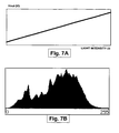
- Figure 7A illustrates the response of a sensor element built using the technology of the present invention.
- the extended dynamic range of the sensor element is sufficient to enable it to respond to impinging radiation with a pixel response over the full range of electromagnetic radiation intensity.
- the sensor element is able to capture sufficient charges in the darkest portion while avoiding the saturation effects in the brightness portions of the image to be captured.
- the net effect is a faithful reproduction of the image to be captured regardless of the intensity of the electromagnetic energy impinging upon the sensor.
- Figure 8 illustrates an exemplary pixel structure of the present invention.
- the pixel structure of Figure 8 uses the conventional signal acquisition structure of Figure 3 but replaces the time domain integrator 110 with a novel phase domain integrator 210.
- Figure 9 shows the phase domain integrator of the present invention in more detail.
- Phase and frequency have a differential relationship.
- the VCO control signal input waveform segment 730 causes the VCO to output waveform segment 710.
- the plot of the VCO output phase as a function of time generates the curve segment 610.
- phase measurement based integration measures the phase traversed by the oscillator output ⁇ during integration time ⁇ T.
- the phase traversed by the oscillator output ⁇ during integration time ⁇ T is proportional to the integral of the input control signal during integration time ⁇ T and the two are proportional.
Landscapes
- Engineering & Computer Science (AREA)
- Multimedia (AREA)
- Signal Processing (AREA)
- Physics & Mathematics (AREA)
- Nonlinear Science (AREA)
- General Physics & Mathematics (AREA)
- Spectroscopy & Molecular Physics (AREA)
- Theoretical Computer Science (AREA)
- Computer Vision & Pattern Recognition (AREA)
- Solid State Image Pick-Up Elements (AREA)
- Analogue/Digital Conversion (AREA)
- Stabilization Of Oscillater, Synchronisation, Frequency Synthesizers (AREA)
- Transforming Light Signals Into Electric Signals (AREA)
- Studio Devices (AREA)
- Light Receiving Elements (AREA)
- Photometry And Measurement Of Optical Pulse Characteristics (AREA)
Description
- This invention relates generally to the field of electronic imaging and more particularly to a method and apparatus for enhanced image capture using photometric measurement and reporting.
- Photography is the process of making pictures by means of the action of light. Light is the commonly used term for electromagnetic radiation in a frequency range that is visible to the human eye. Light patterns reflected or emitted from objects are recorded by an image sensor through a timed exposure. Image sensors can be chemical in nature, such as photographic film, or solid state in nature, such as the CCD and CMOS image sensors employed by digital still and video cameras.
- Digital cameras have a series of lenses that focus light to create an image of a scene. But instead of focusing this light onto a piece of film, as in traditional cameras, it focuses it onto the image sensor which converts the electromagnetic radiation of the light into an electrical charge. The image sensor is said to be a picture element, or a 'pixel.' The electrical charge indicates a relative intensity of the electromagnetic radiation as perceived by the image sensor, and generally is used to associate a light intensity value with the pixel.
-
Figure 1 illustrates typical component blocks that may be included in a digitalimage processing system 10. Thesystem 10 includes asignal source 100 and a signal processing chain that consists ofintegrator 110, analog to digital converter (ADC) 120 and DSP 130.Signal source 100 could for example be a sensor such as a light intensity sensor that generates an electrical response in response to electromagnetic radiation, such as light, impinging upon it. - The output of
integrator 110, VOUT, is input toADC 120. ADC 120 performs the analog to digital conversion function. The analog to digital conversion function is well known in the art. The analog signal VOUT present atADC 120 input is converted into signal VD that can take one of a set of discrete levels. - The quality of the signal is improved by
integrator 110 which integrates the signal VIN.Figure 2 illustrates the nature of the signal improvement.Waveform 200 is the combination of a constant value signal generated bysignal source 100 and additive noise that corrupts the constant value signal.Waveform 210 is the integrator output generated in response toinput signal waveform 200. It is readily observed that signal fluctuations caused by the additive noise decrease inwaveform 210. -
Signal source 100 could be a light intensity sensor that is used in a timed application, such as in a digital camera application where the sensor is exposed to the light for a specific duration of time, commonly referred to as the exposure time. Theintegrator 110 then also serves the function of integrating the response ofsensor 100 caused by all photons received during the exposure time into one value, such as for example a voltage, to be read-out at the end of the exposure time. -
Figures 3 illustrates a typical image sensor circuit.Signal source 1000 is a light sensor that by way of example can be said to be a photodiode. Capacitor 1040 is a simple integrator. The input to the integrator is the output ofsignal source 1000. Capacitor 1040 is reset byswitch 1050 which is in the closed position prior to starting the integration process. At the start of theintegration process switch 1050 opens and the voltage acrosscapacitor 1040 begins to change in response to the input signal originating fromsignal source 1000. At the end of theintegration process switch 1030 closes andintegrator output 1060, VOUT, is sampled.Figure 3 is an illustrative diagram. The implementation of other similar integrators with identical functionality is well known to one skilled in the art. -
Integrator output 1060, VOUT, cannot in general exceed the upper limit imposed by the available power supply voltage. Power supply voltages are decreasing in state-of-the-art equipment due to stringent power consumption requirements.Integrator output 1060 cannot exceed the power supply voltage and will saturate if the integrator output signal continues to build after reaching the power supply voltage level. The saturation condition is illustrated inFigure 4A . Saturation occurs when the output voltage reaches the available power supply voltage and is unable to respond to further changes in the input signal. Signal saturation causes system performance degradation.Figures 4A trough 4C illustrate potential distortions at the output of a pixel structure consisting oflight sensor 100 andintegrator 110 due to dynamic range limitation of the photosensitive element structure and more specifically of the integrator structure. - Segment (a) of
Figure 4A illustrates the linear increase ofintegrator 110 output in response to a constant input signal of different level. The image sensor structure will perform well for the range of input light intensities that give rise to the linear output of segment (a); the image sensor structure will not perform well for the range of input light intensities that give rise to the saturated output of segment (b). - The integrator output response is indicative of limited dynamic range. As illustrated in
Figure 4A the image sensor will render well shadow detail but will fail to render highlight detail. It is possible to shift the response as illustratedFigures 4B and 4C . InFigures 4B and 4C the dynamic range of the image sensor remains the same but the response characteristic is shifted. The response characteristic ofFigure 4B loses shadow and highlight detail but retains good midrange response. The response characteristic ofFigure 4C loses shadow detail and partial midrange detail in order to maintain good highlight detail. -
Figure 5A illustrates the histogram of the pixel intensities of an overexposed image capture where a multitude of pixels were driven into saturation, such as inFigure 4A . As seen inFigure 5A the maximum pixel structure output value is '255' and the units used are theADC 120 output corresponding to the pixel output voltage. The light intensity causedmany light sensors 100 to output a value that saturated theintegrator 110 as the exposure progressed during the exposure period. The maximum (saturated) value of theintegrator 110 output caused the ADC to generate the output code '255' which is the maximum output code for an 8-bit ADC. The image capture will be of lower than optimal quality due to the inability of those pixels subject to high intensity light inputs to achieve a sufficiently high output level. Alower integrator 110 gain would have caused the outputs of the light image sensor subject to high intensity light inputs to register a below-255 output and avoid the high end distortion. -
Figure 5B illustrates the histogram of the pixel intensities of an underexposed image capture where a multitude of pixels were not exposed to sufficient light to achieve a minimum output value. As seen inFigure 5B the minimum pixel structure output value is '0' and the units used are theADC 120 output corresponding to the pixel output voltage. The light intensity causedmany light sensors 100 to output a value that failed to causeintegrator 110 to output a sufficiently high value to cause a minimal ADC output code as the exposure progressed during the exposure period. - The image capture will be of lower than optimal quality due to the inability of those pixels subject to low intensity light inputs to achieve a sufficiently high output level. The distortion illustrated in the histogram of
Figure 5B corresponds to the individual pixel distortion ofFigure 4C . Ahigher integrator 110 gain would have caused the outputs of the light image sensor, subject to low intensity light inputs, to register an above-zero output and avoid the low end distortion. -
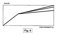
Figure 6 illustrates the response curve of a pixel structure built using double-slope technology. The nonlinear extension of dynamic range illustrated inFigure 6 avoids saturation effects; however, the non-linear relationship between the intensity of the electromagnetic energy impinging upon the sensor and the sensor's output causes the image to be captured with reduced resolution when high levels of light intensity are present. - Other approaches such as multiple exposure combining, conditional slope switching and logarithmic response pixel structures have been published. The multiple exposure combining, conditional slope switching and logarithmic response pixel structures exhibit performance degradations that render them unsuitable for high performance image acquisition tasks.
- Integrator saturation is the limiting factor in the dynamic range performance of a pixel structure. Solutions to the integrator saturation problem have been published. One feature the published solutions have in common is the monitoring of the integrator output to detect the onset of saturation condition at which time the integrator is discharged and the event is recorded. This class of solutions is difficult to implement efficiently in integrated circuits (ICs) due to accuracy requirements of analog components and non-standard analog implementations. The implementation of accurate comparators that operate in a noisy environment near the power supply voltage, where integrator outputs begin to saturate, is a difficult undertaking that consumes excessive power, an undesirable operational feature.
- Analog IC designs are difficult and time consuming to implement. It is advantageous to use standard building blocks that have been fully debugged and optimized for size, power consumption and performance. The class of published solutions does not meet this requirement.
-
WO 00/38409 A1 -
US 5737018 A discloses an exposure device for a video camera in which the gain of an iris which receives the image, the gain of an AGC amplifier which amplifies the sensed image, and the gain of an electronic shutter which controls the speed at which images are sensed, are all controlled based on object luminance. - According to one aspect of the invention, a method for obtaining a high dynamic range read-out signal from a pixel structure comprises the steps of: applying a gain to an input signal provided by a photosensitive element of a pixel structure to provide a gain controlled input signal; forwarding the gain controlled input signal to a phase integrator of the pixel structure, the phase integrator comprising an oscillator and an accumulator for accumulating a number of phases traversed by a signal provided by the oscillator in response to the gain controlled input signal; and wherein the gain applied to the input signal is controlled in response to the number of phases traversed by the signal provided by the oscillator.
- According to another aspect of the invention, a pixel structure comprising: a gain controller for providing a gain controlled signal; and a photosensitive element for generating a signal in response to electromagnetic radiation having an output coupled to an input of the gain controller; and a phase integrator comprising an oscillator coupled to the gain controller to receive the gain controlled signal and provide an output signal to an accumulator, the accumulator generating a phase integrated signal representative of radiation received at the pixel structure.
- With such an arrangement, a solid-state pixel is provided that is capable of producing a faithful reproduction of an image to be captured regardless of the intensity of electromagnetic energy impinging on the sensor and with dynamic gain adjustment capabilities. These and other advantages of the invention will be described with regard to the below figures.
-
-
Figure 1 is a block diagram illustrating exemplary components that may be included in an image sensor and associated processing chain; -
Figure 2 is a graph illustrating the noise smoothing feature at the output of an integrator; -
Figure 3 is a block diagram of a typical pixel structure; -
Figures 4A-4C are transfer curves provided to describe distortions at the output of a pixel structure such as that ofFigure 3 , illustrating dynamic range limitations; -
Figures 5A and 5B are histograms of pixel intensities of respective overexposed and underexposed image capture; -
Figure 6 is a response curve of a pixel structure built using double-slope technology; -
Figure 7A is a response curve of a pixel structure of the present invention; -
Figure 7B illustrates an exemplary histogram of pixel intensities in a captured image of the present invention; -
Figure 8 is a block diagram illustrating exemplary components that may be included in an image sensor and associated processing chain, including a phase domain integrator; -
Figure 9 is a block diagram of one embodiment of a phase domain integrator of the present invention; -
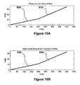
Figures 10A and 10B are graphs illustrating an oscillator phase (9A) and a time domain integrator output signal (9B), and is used to describe the signal integration capabilities of the present invention; -
Figure 11A is a graph which illustrates an oscillator waveform that varies in frequency in response to an oscillator input illustrated inFigure 11B ; -
Figure 12 is a graph illustrating the effects of quantization error on low intensity signals; -
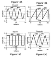
Figures 13A-13D illustrate several common VCO output waveforms; -
Figures 14A and 14B are graphs provided to illustrate a phase unwrapping mechanism of the present invention; -
Figure 15 is a block diagram of a phase domain integrator component of the sensor element of the present invention; -
Figure 16 is a flow diagram provided to illustrate several steps that may be performed during an image capture process by the phase domain integrator ofFigure 15 ; -
Figure 17 illustrates a second embodiment of a phase integrator of the present invention capable of providing a non-linear response to electromagnetic radiation stimulus; -
Figure 18 is a graph illustrating exemplary linear and non-linear integrator responses that may be provided by an integrator of the present invention; -
Figure 19 is an enlargement ofFigure 18 around the origin. - According to one aspect of the invention, a high dynamic range sensitive sensor element or array is provided which uses phase domain integration techniques to accurately capture high and low intensity images. The sensor element of the present invention is not limited by dynamic range characteristics exhibited by prior art solid-state pixel structures and is thus capable of capturing a full spectrum of electromagnetic radiation to provide a high quality output image.
-
Figure 7A illustrates the response of a sensor element built using the technology of the present invention. The extended dynamic range of the sensor element is sufficient to enable it to respond to impinging radiation with a pixel response over the full range of electromagnetic radiation intensity. As a result the sensor element is able to capture sufficient charges in the darkest portion while avoiding the saturation effects in the brightness portions of the image to be captured. The net effect is a faithful reproduction of the image to be captured regardless of the intensity of the electromagnetic energy impinging upon the sensor. -
Figure 7B illustrates the histogram of the pixel intensities of a correctly exposed image capture where all pixel outputs are within the dynamic range of the 8-bit ADC that is zero to 255. - The sensor element of the present invention includes a novel integrator implementation that is based on frequency oscillator circuits. Frequency oscillator circuits are standard IC component blocks and do not suffer the disadvantages of the prior art solid-state devices. Also, the novel sensor element disclosed herein uses accurate integrators that can accommodate output signal values far in excess of available power supply voltages and with very high accuracy and dynamic range.
- For high performance image acquisition it is desirable to have image sensors capable of high resolution and high dynamic range image acquisition using a single sensor read-out step.
Figure 8 illustrates an exemplary pixel structure of the present invention. The pixel structure ofFigure 8 uses the conventional signal acquisition structure ofFigure 3 but replaces thetime domain integrator 110 with a novelphase domain integrator 210.Figure 9 shows the phase domain integrator of the present invention in more detail. - In the present invention, the output of signal source 100 (
Figure 8 ) is connected to theinput 800 of the phase domain integrator ofFigure 9 . At the end of the integration period the integral of the input signal is read in phase format at the phasedomain integrator output 840. - The image sensor assembly and specifically the integrator section satisfy two criteria: a) produce a large output in response to weak input signals from the light sensitive element and b) avoid saturation when the input signals from the light sensitive element are large. These two criteria are mutually exclusive in solid-state structures. However, the present invention realizes that the two criteria can be satisfied through the use of a phase domain integrator such as that of
Figure 9 . - The operation of the phase domain integrator can best be fully understood by exploring the concepts of integration, phase and frequency and their interrelation. The integration function, or integral, is a mathematical function that is well known in the art. Briefly, an integral is a mathematical object that can be interpreted as an area or a generalization of area. If a signal is plotted as a curve, the integral of the signal is the area under the curve. An integrator is a device that integrates a signal present at its input and produces an integrated version of the input signal at its output.
- Phase and frequency have a differential relationship. The total phase traversed by an oscillator output Vout during a duration of time ΔT is mathematically given by

- Separating the integral terms

- For the special case where fnom =0 then K=0 and

- The second term consists of a constant value multiplier fgain and the term ∫ Sin dt which is the integral of the input signal Sin. The term fgain • ∫ Sin dt can be easily obtained by subtracting the value ofK from the Δθ value at the end of the time period ΔT:


- For the special case fnom =0 and therefore K=0

- The relationship above establishes the differential relationship between the VCO control input signal Sin and the phase Δθ traversed by the VCO or oscillator output during a period of time ΔT.
Figures 10A and 10B illustrate this equivalence graphically.Figure 10A plots the phases traversed by the VCO output as a function of time.Figure 10B plots the integral with respect to time of the input control signal SIN. -
Figure 11A illustrates a voltage controlled oscillator output waveform generated in response to an input signal SIN illustrated inFigure 11B . SIN is comprised of two constant value segments, the first segments labeled 720 inFigure 11B being lower in value than the second segments, labeled 730 inFigure 11B . - Referring back to
Figure 10B ,integrator output segment 620 is the integral output as a function of time when the lower value SINsegment 720 was input to the integrator.Integrator output segment 630 is the integral output as a function of time when the higher value SINsegment 730 was input to the integrator. - The lower value SIN
segment 720 caused the VCO to oscillate at a lower frequency than the higher value SINsegment 730.Waveform segment 700 inFigure 11A illustrates the lower VCO oscillation frequency. The highervalue SIN segment 730 at the VCO input causes the VCO to oscillate at a higher frequency than the lower value SIN segment.Waveform segment 710 inFigure 11A illustrates the higher VCO oscillation frequency. -
Figure 10A plots the phases traversed by the VCO as a function of time.Segment 600 corresponds toVCO output segment 700.Segment 610 corresponds toVCO output segment 710.Segment 600 indicates a lower phase accumulation rate thansegment 610. The phase accumulation rate is the integral of the phase traversed by the VCO per unit of time and can be expressed in units of radians per second. The velocity with which the VCO traverses a unit of phase is the frequency of oscillation and is also expressed in units of radians per second. - The VCO control signal
input waveform segment 720 causes the VCO tooutput waveform segment 700. The plot of the VCO output phase as a function of time generates thecurve segment 600. - The VCO control signal
input waveform segment 730 causes the VCO tooutput waveform segment 710. The plot of the VCO output phase as a function of time generates thecurve segment 610. - The waveforms plotted in
Figures 10a and 10b are identical in shape and are related by the constant fgain when fnom =0 and therefore K=0; when fnom≠0 and therefore K≠0 the waveforms plotted inFigures 10A and 10B are related by the constants fgain and K. - Accordingly it is realized that the time domain integral of the input signal SIN is therefore functionally equivalent to the phase domain integral of the input signal SIN. The time domain integral of the input signal SIN and the phase domain integral of the input signal SIN are related through two constants, one of which equals zero for the special case fnom =0.
- The use of the method disclosed herein to perform signal integration has advantages over conventional integrators and resolves difficult performance issues associated with conventional integrators. One advantage is the resolution of the potential to saturate the integrator output. VCO or oscillator outputs are strictly bound by upper and lower limits (peak values) which are not exceeded under any circumstances. Therefore output saturation conditions cannot occur.
- Another advantage is the resolution of the issue of quantization noise. As illustrated in
Figure 12 low level signal 310 could suffer from significant and unacceptable quantization noise, with little distinction between output voltages generated by input intensities close in value. Phase measurement based integration measures the phase traversed by the oscillator output Δθ during integration time ΔT. The phase traversed by the oscillator output Δθ during integration time ΔT is proportional to the integral of the input control signal during integration time ΔT and the two are proportional. The minimum Δθ value occurs for the smallest integral output. But
- where K is a constant. Therefore Δθ - K can be independently set to a specific value for any given value of ∫Sin dt, including its minimum, by simply adjusting the VCO gain fgain. The ability to set the gain of the integrator and hence the minimum value of the measured integrator output variable eliminates the quantization noise issue associated with conventional integrators.
- Yet another advantage is that variable oscillator circuits are common and fundamental building blocks of a wide variety of systems. Therefore they are widely available and have been highly optimized.
- Thus VCO-based integrators are far superior to conventional integrators in quantization noise and dynamic range or lack of output saturation. Other advantages exist and are apparent to one versed in the art.
- Oscillators are a class of circuits well known in the art. The output of oscillator circuits can have a variety of shapes but they are all periodic, meaning that the output waveform is repetitive. One repetition of the output waveform comprises one oscillation cycle and the duration of a cycle is defined as its period of oscillation.
- The frequency of oscillation, fosc, is defined as the number of periods of oscillation per unit time and it is usually measured in Hertz (periods of oscillation per second). By convention the angular frequency of an oscillator is defined as ω = 2πfosc and one complete cycle of oscillation traverses a phase angle θ of 2π radians.
- Associated with an oscillator are initial conditions, that is the state of the system at some arbitrary time, t=0. An example of an initial condition might be the initial phase of the oscillator at t=0 measured in radians.
-
Figures 13A , B, C and D illustrate common output waveforms of oscillator circuits. As well known in the artFigures 13 A, B, C and D illustrate the output waveform of sinusoidal, triangular, sawtooth and square wave oscillators. In all cases the peak voltage range shown is one volt. - The frequency of oscillation of electronic oscillator circuits can be fixed or variable. A common oscillator with variable frequency of oscillation is the voltage-controlled oscillator (VCO). At a minimum a VCO has a voltage input at which a signal voltage Sin controls the frequency of oscillation. Voltage relates to current through Ohm's law and a signal Sin can be said to control the frequency of oscillation through its current rather than voltage characteristic.
- A VCO may also have a nominal frequency of oscillation fnom. The VCO oscillates at fnom when the frequency control input Sin level is not present or of a value that does not modify the frequency of oscillation, such as for example zero volts. The nominal frequency of oscillation can have any specified value including zero Hertz.
- The output frequency of the VCO changes in response to amplitude variations of the input signal. Thus the instantaneous frequency of oscillation of the VCO will differ from the nominal frequency of oscillation of the VCO by some value fdelta and will be given by


- In this example the term fdelta is measured in radians per second, fgain is measured in radians per second per volt and Sin is measured in volts.
- As described above,
figure 11A illustrates the input and output signals of a VCO. The frequency of oscillation of the VCO output changes in response to variations in the input signal amplitude. TheVCO output segment 700 corresponds to inputsignal segment 720. TheVCO output segment 710 corresponds to inputsignal segment 730. The frequency of oscillation ofVCO output segment 700 is lower than the frequency of oscillation ofVCO output segment 710. The amplitude ofinput signal segment 720 is lower than the amplitude ofinput signal segment 730. Therefore fgain has a positive value and the VCO frequency of oscillation is directly proportional to the input control signal amplitude. - A VCO may also have additional inputs, such as RESET/ENABLE. The function of RESET/ENABLE when in the RESET state is to reset the VCO output waveform to a predetermined voltage that can be any value within the peak-to-peak voltage range. The function of RESET/ENABLE when in the ENABLE state is to enable the VCO output to oscillate.
- A VCO has an output Vout. During each period of oscillation Vout traverses an angular phase of 2π radians. This implies that the output phase is measurable modulo 2π and oscillator output values at phases that are separated by exactly 2π are identical.
Figures 13A-12D illustrates several common VCO output waveforms. During a complete period each waveform inFigure 13 traverses exactly 2π radians and waveforms values at phases that are separated by exactly 2π are identical for all waveforms. - The phase traversed by the oscillator output during a subset of one period is determined by sampling the oscillator output at the two instances of time marking the beginning and end of the subset of one period, identifying the phase associated with each sample and subtracting the two phases.
- The phase traversed by the oscillator output during a duration of time that spans more than one period of oscillation can only be determined modulo 2π radians when using a method based on direct observation of the VCO output at two time instances. Thus an additional function is used that counts the number of periods or significant fractions of a period traversed by the VCO output in order to resolve the ambiguity.
- A circuit that counts the number of periods or significant fractions of a period traversed by the VCO output in a time interval, or 'unwraps' the phase, can be readily implemented. Waveforms associated with such a circuit are illustrated in
Figures 14A and 14B . The VCO output inFigure 14A is the triangular waveform. At times t=0, 0.5TP and TP the VCO output waveform reaches states labeled 900, 910 and 920 corresponding to a travel of 0, π and 2π radians. - The output of the phase unwrapping circuit changes states at times t=0, 0.5TP and TP to levels of 0, V and 2V amplitude. The transition times are labeled 930, 940 and 950 and they correspond to the VCO output states labeled 900, 910 and 920, respectively.
- The relationship between the VCO output and the output of the phase unwrapping circuit, illustrated over one period of the VCO output, can be extended over any number of VCO output periods with the output of the phase unwrapping circuit increasing in value by a predetermined amount each time the VCO output goes through its 0 and π (modulo 2π) phase values. It is known to one skilled in the art that there are alternative ways to implement the phase unwrapping function and mark the value of the unwrapped phase traversed by the VCO output.
- The total phase traversed by the VCO output is given by the summation of two terms. The first term is the total unwrapped phase recorded by the phase unwrapping circuit. The second term is the total phase traversed by the VCO output since the last update of the phase unwrapping circuit output. This quantity can be unambiguously obtained by direct measurement of the VCO output.
-
Figure 15 incorporates a simplified block diagram of the VCO subset of ICL8038 a commercially available IC. Additional phase unwrapping, total phase traversed and VCO RESET/ENABLE functions are added. -
Current sources capacitor 845. The charging and discharging ofcapacitor 845 is determined byswitch 865 which is controlled by flip-flop 825 and which connectscurrent source capacitor 845. - Flip-
flop 825 changes states when triggered bycomparators Comparator 815 is triggered whencapacitor 845 reaches a predetermined high voltage.Comparator 820 is triggered whencapacitor 845 reaches a predetermined low voltage. - When
comparator 815 is triggered flip-flop 825 changes state such as to causeswitch 865 to close. Current I2 ofcurrent source 860 causescapacitor 845 to discharge thus causing the voltage acrosscapacitor 845 to decrease. The decrease of the voltage acrosscapacitor 845 immediately causescomparator 815 to change state. - When the voltage across
capacitor 845 decreases to a sufficientlylow value comparator 820 is triggered. Whencomparator 820 is triggered flip-flop 825 changes state such as to causeswitch 865 to open. Current I1 ofcurrent source 855 causescapacitor 845 to charge thus causing the voltage acrosscapacitor 845 to increase. The increase of the voltage acrosscapacitor 845 immediately causescomparator 820 to change state. - When the voltage across
capacitor 845 increases to a sufficientlyhigh value comparator 815 is again triggered causing flip-flop 825 to change state andcapacitor 845 charge/discharge cycle to repeat. - The relationship between the charge held by
capacitor 845 and the voltage acrosscapacitor 845 is Q=C·V where C is the capacitance ofcapacitor 845 measured in Farads, Q is the charge held bycapacitor 845 measured in Coulombs and V is the voltage acrosscapacitor 845 measured in Volts. - The change in charge held by
capacitor 845 due to a constant current I that flows for an interval of time ΔT is given by ΔQ=I·ΔT where ΔQ is the change in charge held bycapacitor 845 in Coulombs, I is the value of the current in Amperes and ΔT is the interval of time of current flow in seconds. A constant current causes a linear change in the charge held bycapacitor 845 as a function of time. The linear change in the charge held bycapacitor 845 as a function of time causes a linear change in voltage acrosscapacitor 845 as a function of time. - The constant value of currents I1 and I2 generated by
current sources 855 and 866 causes the voltage acrosscapacitor 845 to increase and decrease linearly generating a triangular waveform. If the net effects of currents I1 and I2 are equal the rising and falling segments of the triangular voltage waveform acrosscapacitor 845 are symmetric as illustrated inFigure 6c . If the net effects of currents I1 and I2 are not equal the rising and falling segments of the triangular voltage waveform acrosscapacitor 845 are asymmetric. In the limit as the net effects of current I1 << the net effects of current I2 the triangular voltage waveform acrosscapacitor 845 tends to the sawtooth waveform illustrated inFigure 6b . - The time to charge and discharge
capacitor 845 is determined by the magnitude of currents I1 and I2 generated bycurrent sources capacitor 845 to voltage levels that triggercomparators - The control signal applied at
input 870 controlscurrent sources current sources - Reversal of the voltage across
capacitor 845 is controlled by the state of flip-flop 825.Counter 835 is triggered and modifies its output state correspondingly each time flip-flop 825 changes state. The change incounter 835 output state can be a modified voltage level as shown inFigure 8b . Other voltage level modification schemes can be used as long as separate states are resolvable.Counter 835 output can also be of a digital format consisting of a digital word containing B bits. In such case a change in its output state can be a binary number where different states differ in one or more bits. - The output state of
counter 835 changes each time flip-flop 825 changes states and therefore counts how many times the VCO output reached its minimum and maximum values. If the output state ofcounter 835 is an even number the output of the VCO traversed an integer multiple of 2π radians. The number of 2π radians traversed by the VCO output is then given by dividing the output count ofcounter 835 by two. - If the output state of
counter 835 is an odd number the number of 2π radians traversed by the output of the VCO has an integer and a fractional part. The integer part of the number of 2π radians traversed by the output of the VCO is given by dividing by two a number obtained by subtracting one from the output state ofcounter 835. The fractional part of the number of 2π radians traversed by the output of the VCO depends on the degree of asymmetry between the rising and falling segments of the waveform and can be readily obtained by one skilled in the art. By way of example if the rising segment of the waveform takes twice as long as the falling segment of the waveform than then it requires 2/3 of a period of oscillation to complete. - The voltage across
capacitor 845 is proportional to the phase traversed by the VCO output following the last change in state of flip-flop 825. It can be readily obtained by one skilled in the art if a) the trigger voltages ofcomparators 815 and 820 (i.e., the maximum and minimum voltages of the VCO output) and b) the asymmetry between the rising and falling segments of the VCO output waveform are known. By way of example consider that if a) the VCO output voltage is halfway between the minimum and maximum value on the rising segment of the waveform and b) the rising segment of the waveform takes twice as long as the falling segment of the waveform then the waveform measurement is at 1/3 of a period of oscillation. - The total phase traversed by the output of the VCO is obtained by summing the phase traversed by the VCO output as recorded by the voltage to phase
converter 840 and by counter andphase converter 835. This function is performed bysummer 880 and made available atoutput 890. - Switch 850 resets
capacitor 845 and therefore the VCO oscillator output to an initial voltage output byvoltage source 810. Flip-flop 825 is reset bysignal 895. The initial voltage ofvoltage source 810 together with the reset state of flip-flop 825 and the degree of asymmetry between the rising and falling segments of the VCO output waveform are sufficient to determine the initial phase of the VCO output waveform. This derivation is well known to one versed in the art. - As well known in the art and described in the ICL8038 application notes literature sinusoidal, square and sawtooth waveforms are derived by additional internal circuits using the basic triangular waveform discussed herein. Therefore the items addressed herein apply equally to other VCO output waveform shapes.
- The present invention thus replaces the conventional integrator component of a pixel structure with a high gain and high dynamic range integrator that performs the time integration of the input signal in the phase domain.
-
Figure 16 is a flow diagram which illustrates several exemplary steps that may be performed during acapture process 150 by a pixel structure that uses the phase domain integrator of the present invention. - At the beginning of said exposure time (step 151), the VCO output and the counter and
phase converter 835 are reset. Atstep 152 the photosensitive element is exposed to light and changes its electrical characteristics causing the VCO output to change frequency. The photosensitive element can be any element such as a photodiode, a photogate, a phototransistor or a photoresistor. The present invention is also related to a solid-state imaging device, such as a CMOS or MOS imaging device having a geometric configuration of pixels, at least part of the pixels having the structure described above. - At
step 153 counter andphase converter 835 records the unwrapped phase traversed by the VCO output. When it is determined atstep 154 that the exposure frame ends the output of the VCO is translated to radians by voltage to phaseconverter 840 atstep 155. The outputs of the counter andphase converter 835 and voltage to phaseconverter 840 are added bytotal phase adder 880. Atstep 156 the phase domain integration result may be translated to the time domain integration result if so desired. Step 156 is shown in dashed lines to indicate that it is not a necessary step of the capture process. - Accordingly a method and apparatus for constructing a pixel structure having a high dynamic range has been described.
Figures 9 ,10A and 10B illustrate an exemplary embodiment and operation of one pixel structure of the invention which provides a generally linear integration response to input stimulus. According to another aspect of the invention, the integral output can also follow a non-linear characteristic where, by way of example and assuming a constant value input, a doubling of the integration time will not result in a doubling of the integral output value. By way of example, a nonlinear integral output can have an output characteristic related to an exponential function which is non-linear. - Any exponential function has the characteristic that its rate of growth (slope) is proportional to its value within a constant of proportionality.
Figure 17 illustrates a second embodiment of a phase domain integrator which is similar to that ofFigure 3b , modified to provide a rate of change of the integrator output value that is controlled by the integrator output value itself. Specifically, in the phase domain integrator ofFigure 17 the integrator output (the total phase traveled) can control the gain of the integrator and hence the rate of change of the integrator output -
Gain block 1805 can have a wide range of functional characteristics. For example, assume the gain ofblock 1805 is the inverse ofinput voltage 1860. Asinput voltage 1860 increases the gain ofblock 1805 decreases. Assuming a constant input 1800 (SIN) the rate of increase ofintegrator output 1840 will decrease ascontrol voltage 1860 increases and the gain ofgain block 1805 decreases. - As illustrated in
Figure 17 switch 1850 can selectsignal 1840 orsignal 1845 to control thegain block 1805.Signal 1840 is a continuous signal whilesignal 1845 is a discontinuous staircase signal. For the examples illustrated here switch 1850 selectssignal 1845 to controlgain block 1805. - In one embodiment,
gain block 1805 is proportional to the inverse of the integrator output value. Thus the gain ofgain block 1805 is the inverse ofsignal 1860 which is the output ofswitch 1850.Signal 1855 is the integrator input and equals the value of signal 1800 (SIN) multiplied bygain block 1805. As theintegrator output 1860 selected byswitch 1850 increases in value, the gain ofgain block 1855 decreases. For a constant value signal input 1800 (SIN) signal 1855 decreases causing the phase domain integrator output to increase at a lower rate. -
Figure 18 illustrates the output of an integrator function with linear (1700) and non-linear (1710) characteristic and with constant input. Curve labeled 1700 illustrates a linear integrator output characteristic and shows that a doubling of the integration time results in a doubling of the integrator output value. Curve labeled 1710 illustrates the nonlinear integrator output characteristic and shows that a doubling of the integration time does not result in a doubling of the integrator output value. InFigure 19 ,curve 1710 is the integrator output for the case where the rate of change of the integrator output is controlled be thediscontinuous staircase signal 1845 through an inverse relationship, i.e., the rate of change of the integrator output is proportional to the inverse of the integrator output represented bysignal 1845. -
Figure 19 is an enlargement ofFigure 18 around the origin. Curve labeled 1720 illustrates the linear integrator output characteristic. Curve labeled 1730 illustrates the nonlinear integrator output characteristic. The two curves are identical for the initial portion of the curve that arbitrarily starts at time=1 and ends at time=2 (on the abscissa) and diverge thereafter. At that time the integratoroutput value curve 1730 equaled its initial value of one (the integrator output is shifted by one in order to avoid the potential gain nonlinearity. The final output will remove the initial value shift). - As evident in
Figure 19 the linear integrator output characteristic ofcurve 1700 increases linearly with time, since the input signal is assumed to be constant. As the integrator output increases andoutput component 1845 increases in value in a staircase fashion, the rate of increase of the integrator output decreases in the same staircase fashion. This is evident fromcurve 1710 offigure 18 . - At time t=16 the linear integrator output reaches a value of 16 in this example. At time t=16 the nonlinear integrator output reaches a value of 6 in this example. Decreasing the rate of change of the integrator output as it increases in value advantageously reduces the number of states to encode for the final integrator value. In this example the linear integrator reached a value of 16 that requires an ADC with 5-bit output to encode while the nonlinear integrator only reached a value of 6 that requires an ADC with 3-bit output to encode. Neither device entered into the output saturation state.
- Thus
Figures 17-19 illustrate a method and apparatus by which the gain of the pixel structure can be controlled in response to pixel structure feedback. AlthoughFigure 17 described the use of a gain characteristic that the inverse of the integrator output, the present invention is not limited to any particular gain characteristic, and it is envisioned that there may be embodiments of a pixel structure of the invention with different, fixed, variable and/or adaptive gains which may be selected to meet design requirements. In addition, althoughFigure 17 illustrates that the feedback is directly tied to an integrator output, it is appreciated that there may be design modifications made to process the integrator value in different ways to provide feedback to the gain device. Thus the present invention is not limited to any particular type of feedback, but rather encompasses the idea that feedback may be provided to the integrator to adjust integrator gain based on observed system conditions. - According a method and apparatus has been described for obtaining a read-out signal of a solid-state pixel structure (including CCD, CMOS and MOS-based pixel structures). The pixel structure includes at least a photosensitive element with an output node, means to integrate the output node signal in the phase domain and means to read the phase domain integration value. As described above, a means may also be provided for adjusting a gain of the integrator in response to observed system conditions. The use of the method disclosed herein to perform signal integration has advantages over conventional integrators and resolves difficult performance issues associated with conventional integrators. One advantage is the resolution of the potential to saturate the integrator output. VCO or oscillator outputs are strictly bound by upper and lower limits (peak values) which are not exceeded under any circumstances. Therefore output saturation conditions cannot occur. With such an arrangement a solid-state pixel is provided that is capable of producing a faithful reproduction of an image to be captured regardless of the intensity of electromagnetic energy impinging on the sensor.
- Having described various embodiments of the invention, it will be appreciate that although certain components and process steps have been described the descriptions are representative only; other functional delineations or additional steps and components can be added by one of skill in the art, and thus the present invention should not be limited to the specific embodiments disclosed. The various representational elements may be implemented in hardware, software running on a computer, or a combination thereof and modification to and variation of the illustrated embodiments may be made without departing from the inventive concepts herein disclosed. Accordingly, the invention should not be viewed as limited except by the scope of the appended claims.
Claims (18)
- A method for obtaining a high dynamic range read-out signal from a pixel structure comprising the steps of:applying a gain to an input signal (1800) provided by a photosensitive element of a pixel structure to provide a gain controlled input signal (1855);forwarding the gain controlled input signal (1855) to a phase integrator of the pixel structure, the phase integrator comprising a voltage controlled oscillator and an accumulator (1830) for accumulating a number of periods of the phases traversed by a signal provided by the oscillator in response to the gain controlled input signal (1855); andwherein the gain applied to the input signal (1800) is controlled in response to the number of phases traversed by the signal (1810) provided by the oscillator.
- The method of claim 1, wherein the gain is constant.
- The method of claim 1, wherein the gain is non-constant.
- The method of claim 1, wherein the non-constant gain varies in accordance with a continuous output of the accumulator (1830).
- The method of claim 3, wherein the non-constant gain is a discontinuous output of the accumulator (1830).
- The method of claim 1, wherein the accumulator (1830) accumulates phases of the oscillator during an exposure period, and wherein the gain varies during the exposure period.
- The method of claim 1, wherein the gain is proportional to an inverse of an output of the phase integrator.
- The method of claim 1, wherein the gain is proportional to an output of the phase integrator.
- A pixel structure comprising:a gain controller (1805) for providing a gain controlled signal (1855); anda photosensitive element for generating a signal (1800) in response to electromagnetic radiation having an output coupled to an input of the gain controller (1805); anda phase integrator comprising a voltage controlled oscillator coupled to the gain controller (1805) to receive the gain controlled signal (1855) and provide an output signal (1810) to an accumulator (1830), the accumulator (1830) generating a phase integrated signal (1840) by accumulating a number of periods of the phases traversed by the signal provided by the oscillator, representative of radiation received at the pixel structure.
- The pixel structure of claim 9, wherein the gain controller (1805) applies a constant gain to the signal provided by the photosensitive element.
- The pixel structure of claim 9, wherein the gain controller (1805) applies a non-constant gain to the signal provided by the photosensitive element.
- The pixel structure of claim 11, wherein the non-constant gain is related to an output of the phase integrator of the pixel structure.
- The pixel structure of claim 11, wherein the non-constant gain is related to a continuous output of the accumulator (1830) of the phase integrator.
- The pixel structure of claim 11, wherein the non-constant gain is related to a discontinuous output of the accumulator (1830) of the integrator.
- The pixel structure of claim 9, wherein the accumulator (1830) accumulates phases of the oscillator during an exposure period, and wherein the gain varies during the exposure period.
- The pixel structure of claim 9, wherein the gain is proportional to an inverse of an output of the phase integrator.
- The pixel structure of claim 9, wherein the gain is proportional to an output of the phase integrator.
- The pixel structure of claim 9, wherein the phase integrator is coupled to the photosensitive element for integrating the response of the photosensitive element to the electromagnetic radiation over an exposure time period using phase information.
Applications Claiming Priority (5)
| Application Number | Priority Date | Filing Date | Title |
|---|---|---|---|
| US71930605P | 2005-09-21 | 2005-09-21 | |
| US71930505P | 2005-09-21 | 2005-09-21 | |
| US71930405P | 2005-09-21 | 2005-09-21 | |
| US72789705P | 2005-10-18 | 2005-10-18 | |
| PCT/US2006/036785 WO2007035858A2 (en) | 2005-09-21 | 2006-09-21 | System and method for a high dynamic range sensitive sensor element or array with gain control |
Publications (3)
| Publication Number | Publication Date |
|---|---|
| EP1935018A2 EP1935018A2 (en) | 2008-06-25 |
| EP1935018A4 EP1935018A4 (en) | 2009-09-23 |
| EP1935018B1 true EP1935018B1 (en) | 2014-05-21 |
Family
ID=37889530
Family Applications (4)
| Application Number | Title | Priority Date | Filing Date |
|---|---|---|---|
| EP06815082.0A Not-in-force EP1935018B1 (en) | 2005-09-21 | 2006-09-21 | System and method for a high dynamic range sensitive sensor element or array with gain control |
| EP20060815089 Ceased EP1938060A4 (en) | 2005-09-21 | 2006-09-21 | System and method for image sensor element or array with photometric and realtime reporting capabilities |
| EP06815090A Ceased EP1938059A4 (en) | 2005-09-21 | 2006-09-21 | System and method for a high dynamic range sensitive sensor element or array |
| EP06836131A Ceased EP1938584A4 (en) | 2005-09-21 | 2006-09-21 | High resolution and wide dynamic range integrator |
Family Applications After (3)
| Application Number | Title | Priority Date | Filing Date |
|---|---|---|---|
| EP20060815089 Ceased EP1938060A4 (en) | 2005-09-21 | 2006-09-21 | System and method for image sensor element or array with photometric and realtime reporting capabilities |
| EP06815090A Ceased EP1938059A4 (en) | 2005-09-21 | 2006-09-21 | System and method for a high dynamic range sensitive sensor element or array |
| EP06836131A Ceased EP1938584A4 (en) | 2005-09-21 | 2006-09-21 | High resolution and wide dynamic range integrator |
Country Status (5)
| Country | Link |
|---|---|
| US (5) | US7800669B2 (en) |
| EP (4) | EP1935018B1 (en) |
| JP (4) | JP4699524B2 (en) |
| KR (4) | KR101152859B1 (en) |
| WO (4) | WO2007035858A2 (en) |
Families Citing this family (29)
| Publication number | Priority date | Publication date | Assignee | Title |
|---|---|---|---|---|
| EP1935018B1 (en) * | 2005-09-21 | 2014-05-21 | RJS Technology, Inc. | System and method for a high dynamic range sensitive sensor element or array with gain control |
| DE102007036973A1 (en) | 2007-02-24 | 2008-09-04 | Fraunhofer-Gesellschaft zur Förderung der angewandten Forschung e.V. | A pixel cell, a method of operating a pixel cell, a method of determining a position of a maximum of an envelope of an analog amplitude modulated signal, a device for determining a charge amount, apparatus and method for determining an amount of charge on a capacitive element, apparatus and method, and setting a circuit node a predetermined voltage, apparatus and method for charge-based analog / digital conversion and apparatus and method for charge-based signal processing |
| WO2010016449A1 (en) | 2008-08-08 | 2010-02-11 | Semiconductor Energy Laboratory Co., Ltd. | Photoelectric conversion device and electronic device having the same |
| WO2011086829A1 (en) * | 2010-01-15 | 2011-07-21 | Semiconductor Energy Laboratory Co., Ltd. | Semiconductor device and electronic device |
| WO2012093387A2 (en) * | 2011-01-09 | 2012-07-12 | Emza Visual Sense Ltd. | Pixel design with temporal analysis capabilities for scene interpretation |
| US10197501B2 (en) | 2011-12-12 | 2019-02-05 | Kla-Tencor Corporation | Electron-bombarded charge-coupled device and inspection systems using EBCCD detectors |
| EP2815393B1 (en) * | 2012-02-14 | 2023-04-05 | Gentex Corporation | High dynamic range imager system |
| JP6041500B2 (en) * | 2012-03-01 | 2016-12-07 | キヤノン株式会社 | Imaging device, imaging system, driving method of imaging device, and driving method of imaging system |
| KR101629881B1 (en) * | 2012-03-16 | 2016-06-13 | 엠파이어 테크놀로지 디벨롭먼트 엘엘씨 | Low light adaptive imaging device |
| KR101895415B1 (en) | 2012-03-27 | 2018-09-06 | 삼성전자주식회사 | Anlaog-to-digital converting circuit and accumulation circuit including the same |
| US9496425B2 (en) | 2012-04-10 | 2016-11-15 | Kla-Tencor Corporation | Back-illuminated sensor with boron layer |
| US9601299B2 (en) | 2012-08-03 | 2017-03-21 | Kla-Tencor Corporation | Photocathode including silicon substrate with boron layer |
| US9426400B2 (en) | 2012-12-10 | 2016-08-23 | Kla-Tencor Corporation | Method and apparatus for high speed acquisition of moving images using pulsed illumination |
| US9478402B2 (en) | 2013-04-01 | 2016-10-25 | Kla-Tencor Corporation | Photomultiplier tube, image sensor, and an inspection system using a PMT or image sensor |
| US9347890B2 (en) | 2013-12-19 | 2016-05-24 | Kla-Tencor Corporation | Low-noise sensor and an inspection system using a low-noise sensor |
| US9748294B2 (en) | 2014-01-10 | 2017-08-29 | Hamamatsu Photonics K.K. | Anti-reflection layer for back-illuminated sensor |
| US9410901B2 (en) | 2014-03-17 | 2016-08-09 | Kla-Tencor Corporation | Image sensor, an inspection system and a method of inspecting an article |
| US9767986B2 (en) | 2014-08-29 | 2017-09-19 | Kla-Tencor Corporation | Scanning electron microscope and methods of inspecting and reviewing samples |
| US9860466B2 (en) | 2015-05-14 | 2018-01-02 | Kla-Tencor Corporation | Sensor with electrically controllable aperture for inspection and metrology systems |
| US10748730B2 (en) | 2015-05-21 | 2020-08-18 | Kla-Tencor Corporation | Photocathode including field emitter array on a silicon substrate with boron layer |
| US10462391B2 (en) | 2015-08-14 | 2019-10-29 | Kla-Tencor Corporation | Dark-field inspection using a low-noise sensor |
| US10313622B2 (en) | 2016-04-06 | 2019-06-04 | Kla-Tencor Corporation | Dual-column-parallel CCD sensor and inspection systems using a sensor |
| US10778925B2 (en) | 2016-04-06 | 2020-09-15 | Kla-Tencor Corporation | Multiple column per channel CCD sensor architecture for inspection and metrology |
| TWI611282B (en) * | 2017-01-03 | 2018-01-11 | 友達光電股份有限公司 | Power Supply Circuit And Power Supplying Method |
| US11114489B2 (en) | 2018-06-18 | 2021-09-07 | Kla-Tencor Corporation | Back-illuminated sensor and a method of manufacturing a sensor |
| US10943760B2 (en) | 2018-10-12 | 2021-03-09 | Kla Corporation | Electron gun and electron microscope |
| US11114491B2 (en) | 2018-12-12 | 2021-09-07 | Kla Corporation | Back-illuminated sensor and a method of manufacturing a sensor |
| US11848350B2 (en) | 2020-04-08 | 2023-12-19 | Kla Corporation | Back-illuminated sensor and a method of manufacturing a sensor using a silicon on insulator wafer |
| CN117490838B (en) * | 2024-01-03 | 2024-03-19 | 成都善思微科技有限公司 | High-reliability flat panel detector data acquisition method, system and computer |
Family Cites Families (67)
| Publication number | Priority date | Publication date | Assignee | Title |
|---|---|---|---|---|
| US682145A (en) * | 1901-04-23 | 1901-09-03 | William J Jones | Apparatus for carbonating liquids. |
| US4352210A (en) * | 1980-09-12 | 1982-09-28 | General Electric Company | Linear mixer with reduced spurious responses |
| JPS5795771A (en) * | 1980-12-05 | 1982-06-14 | Fuji Photo Film Co Ltd | Solid-state image pickup device |
| US4419692A (en) * | 1981-12-31 | 1983-12-06 | Texas Medical Instruments, Inc. | High speed infrared imaging system |
| US4629879A (en) * | 1984-06-11 | 1986-12-16 | Eastman Kodak Company | Light beam intensity controlling apparatus |
| JPS6313520A (en) * | 1986-07-04 | 1988-01-20 | Sony Corp | Analog-digital conversion circuit |
| US4825144A (en) | 1987-11-10 | 1989-04-25 | Motorola, Inc. | Dual channel current mode switching regulator |
| JP2720478B2 (en) | 1988-10-18 | 1998-03-04 | 株式会社ニコン | Photometric device using solid-state imaging device with vertical overflow drain |
| US5416616A (en) * | 1990-04-06 | 1995-05-16 | University Of Southern California | Incoherent/coherent readout of double angularly multiplexed volume holographic optical elements |
| KR100396203B1 (en) * | 1993-06-17 | 2003-12-31 | 소니 가부시끼 가이샤 | Exposure apparatus and method, video camera having the exposure apparatus |
| US5461426A (en) | 1993-08-20 | 1995-10-24 | Samsung Electronics Co., Ltd. | Apparatus for processing modified NTSC television signals, with digital signals buried therewithin |
| KR0168451B1 (en) | 1994-03-31 | 1999-01-15 | 다까노 야스아끼 | Color solid image sensing device |
| DE4423214C2 (en) * | 1994-07-01 | 1998-02-12 | Harris Corp | Multinorm decoder for video signals and method for decoding video signals |
| JPH1022489A (en) * | 1996-07-02 | 1998-01-23 | Fuji Xerox Co Ltd | Solid-state image pickup device |
| WO1998014002A1 (en) * | 1996-09-27 | 1998-04-02 | Boehm Markus | Local auto-adaptive optic sensor |
| US5794922A (en) * | 1996-12-13 | 1998-08-18 | Meglino; Don A. | Fence slats with locking portions |
| US5796392A (en) * | 1997-02-24 | 1998-08-18 | Paradise Electronics, Inc. | Method and apparatus for clock recovery in a digital display unit |
| JP3697678B2 (en) * | 1997-05-09 | 2005-09-21 | ローム株式会社 | V / F conversion circuit |
| EP1031087A1 (en) * | 1997-07-18 | 2000-08-30 | Net Exchange, Inc. | Apparatus and method for effecting correspondent-centric electronic mail |
| US6229133B1 (en) * | 1997-10-27 | 2001-05-08 | Texas Instruments Incorporated | Image sensing device with delayed phase frequency modulation |
| US6452633B1 (en) * | 1998-02-26 | 2002-09-17 | Foveon, Inc. | Exposure control in electronic cameras by detecting overflow from active pixels |
| US6529241B1 (en) * | 1998-02-27 | 2003-03-04 | Intel Corporation | Photodetecting device supporting saturation detection and electronic shutter |
| US20020176009A1 (en) | 1998-05-08 | 2002-11-28 | Johnson Sandra Marie | Image processor circuits, systems, and methods |
| US6188056B1 (en) * | 1998-06-24 | 2001-02-13 | Stmicroelectronics, Inc. | Solid state optical imaging pixel with resistive load |
| US6396561B1 (en) * | 1998-11-10 | 2002-05-28 | Maniabarco N.V. | Method and device for exposing both sides of a sheet |
| US6249807B1 (en) * | 1998-11-17 | 2001-06-19 | Kana Communications, Inc. | Method and apparatus for performing enterprise email management |
| US6757018B1 (en) * | 1998-12-18 | 2004-06-29 | Agilent Technologies, Inc. | CMOS image sensor with pixel level gain control |
| US6654787B1 (en) * | 1998-12-31 | 2003-11-25 | Brightmail, Incorporated | Method and apparatus for filtering e-mail |
| US6777663B2 (en) * | 1999-05-07 | 2004-08-17 | Intel Corporation | Enhanced Photocell with sample and hold amplifier |
| US7123301B1 (en) * | 1999-06-11 | 2006-10-17 | Analog Devices, Inc. | Pixel gain amplifier |
| US6400810B1 (en) * | 1999-07-20 | 2002-06-04 | Ameritech Corporation | Method and system for selective notification of E-mail messages |
| JP3903361B2 (en) * | 1999-08-13 | 2007-04-11 | 日本放送協会 | Solid-state imaging device |
| US7133074B1 (en) * | 1999-09-28 | 2006-11-07 | Zoran Corporation | Image sensor circuits including sampling circuits used therein for performing correlated double sampling |
| JP4550957B2 (en) * | 1999-11-15 | 2010-09-22 | 浜松ホトニクス株式会社 | Photodetector |
| EP1113254A1 (en) | 1999-12-30 | 2001-07-04 | STMicroelectronics S.r.l. | A circuit and a method for extending the output voltage range of an integrator circuit |
| US6882367B1 (en) * | 2000-02-29 | 2005-04-19 | Foveon, Inc. | High-sensitivity storage pixel sensor having auto-exposure detection |
| US6438215B1 (en) * | 2000-02-29 | 2002-08-20 | Ameritech Corporation | Method and system for filter based message processing in a unified messaging system |
| JP4011818B2 (en) * | 2000-02-29 | 2007-11-21 | キヤノン株式会社 | Semiconductor solid-state imaging device |
| JP3753925B2 (en) * | 2000-05-12 | 2006-03-08 | 株式会社ルネサステクノロジ | Semiconductor integrated circuit |
| US7032023B1 (en) * | 2000-05-16 | 2006-04-18 | America Online, Inc. | Throttling electronic communications from one or more senders |
| US6654594B1 (en) * | 2000-05-30 | 2003-11-25 | Motorola, Inc. | Digitized automatic gain control system and methods for a controlled gain receiver |
| AU2001275880A1 (en) * | 2000-07-10 | 2002-01-21 | Silicon Laboratories, Inc. | Digitally-synthesized loop filter circuit particularly useful for a phase locked loop |
| WO2002007587A2 (en) * | 2000-07-14 | 2002-01-31 | Xillix Technologies Corporation | Compact fluorescent endoscopy video system |
| JP3840050B2 (en) * | 2000-11-01 | 2006-11-01 | キヤノン株式会社 | Electromagnetic wave converter |
| US6580496B2 (en) * | 2000-11-09 | 2003-06-17 | Canesta, Inc. | Systems for CMOS-compatible three-dimensional image sensing using quantum efficiency modulation |
| US20020113887A1 (en) * | 2001-02-16 | 2002-08-22 | Iimura Russell M. | CMOS image sensor with extended dynamic range |
| JP3852324B2 (en) * | 2001-02-20 | 2006-11-29 | ティアック株式会社 | Signal processing circuit and signal processing method |
| US7176962B2 (en) * | 2001-03-01 | 2007-02-13 | Nikon Corporation | Digital camera and digital processing system for correcting motion blur using spatial frequency |
| AU2002339874A1 (en) * | 2001-05-23 | 2002-12-03 | Canesta, Inc. | Enhanced dynamic range conversion in 3-d imaging |
| US6867693B1 (en) | 2001-07-25 | 2005-03-15 | Lon B. Radin | Spatial position determination system |
| US7176976B2 (en) * | 2001-08-30 | 2007-02-13 | Lightsurf Technologies, Inc. | Autoexposure methodology in a digital camera |
| US6849841B2 (en) * | 2001-09-28 | 2005-02-01 | Raytheon Company | System and method for effecting high-power beam control with outgoing wavefront correction utilizing holographic sampling at primary mirror, phase conjugation, and adaptive optics in low power beam path |
| US6809358B2 (en) * | 2002-02-05 | 2004-10-26 | E-Phocus, Inc. | Photoconductor on active pixel image sensor |
| JP4086514B2 (en) | 2002-02-13 | 2008-05-14 | キヤノン株式会社 | Photoelectric conversion device and imaging device |
| US20030184673A1 (en) | 2002-04-02 | 2003-10-02 | Michael Skow | Automatic exposure control for digital imaging |
| US7031409B2 (en) * | 2002-08-23 | 2006-04-18 | Samsung Electronics Co., Ltd. | Fully digital AGC circuit with wide dynamic range and method of operation |
| US7277129B1 (en) * | 2002-10-31 | 2007-10-02 | Sensata Technologies, Inc. | Pixel design including in-pixel correlated double sampling circuit |
| CN100388764C (en) * | 2002-11-07 | 2008-05-14 | 罗姆股份有限公司 | Area image sensor |
| KR100920353B1 (en) | 2003-03-14 | 2009-10-07 | 삼성전자주식회사 | Device of driving light device for display device |
| US20050057670A1 (en) * | 2003-04-14 | 2005-03-17 | Tull Damon L. | Method and device for extracting and utilizing additional scene and image formation data for digital image and video processing |
| CN1823336A (en) * | 2003-05-07 | 2006-08-23 | Dvip多媒体股份有限公司 | A method and device for sensor level image distortion abatement |
| JP2005244311A (en) * | 2004-02-24 | 2005-09-08 | Canon Inc | Imaging unit, control method of imaging unit, and control program |
| US6972995B1 (en) * | 2004-04-09 | 2005-12-06 | Eastman Kodak Company | Imaging cell with a non-volatile memory that provides a long integration period and method of operating the imaging cell |
| JP4664017B2 (en) * | 2004-07-12 | 2011-04-06 | 浜松ホトニクス株式会社 | Optical semiconductor integrated circuit device |
| US7489351B2 (en) * | 2005-01-21 | 2009-02-10 | Bae Systems Information And Electronic Systems Integration Inc. | Dynamic range extension for focal plane arrays |
| US7560679B1 (en) * | 2005-05-10 | 2009-07-14 | Siimpel, Inc. | 3D camera |
| EP1935018B1 (en) * | 2005-09-21 | 2014-05-21 | RJS Technology, Inc. | System and method for a high dynamic range sensitive sensor element or array with gain control |
-
2006
- 2006-09-21 EP EP06815082.0A patent/EP1935018B1/en not_active Not-in-force
- 2006-09-21 WO PCT/US2006/036785 patent/WO2007035858A2/en active Application Filing
- 2006-09-21 EP EP20060815089 patent/EP1938060A4/en not_active Ceased
- 2006-09-21 WO PCT/US2006/036794 patent/WO2007035861A2/en active Search and Examination
- 2006-09-21 US US11/533,851 patent/US7800669B2/en not_active Expired - Fee Related
- 2006-09-21 JP JP2008532376A patent/JP4699524B2/en not_active Expired - Fee Related
- 2006-09-21 JP JP2008532373A patent/JP4537483B2/en not_active Expired - Fee Related
- 2006-09-21 KR KR1020087009556A patent/KR101152859B1/en active IP Right Grant
- 2006-09-21 KR KR1020087009542A patent/KR101003054B1/en active IP Right Grant
- 2006-09-21 KR KR1020087009532A patent/KR100970599B1/en active IP Right Grant
- 2006-09-21 US US11/533,859 patent/US7532145B2/en not_active Expired - Fee Related
- 2006-09-21 WO PCT/US2006/036786 patent/WO2007044191A2/en active Application Filing
- 2006-09-21 WO PCT/US2006/036793 patent/WO2007035860A2/en active Search and Examination
- 2006-09-21 US US11/533,870 patent/US7782369B2/en not_active Expired - Fee Related
- 2006-09-21 JP JP2008532377A patent/JP5059767B2/en not_active Expired - Fee Related
- 2006-09-21 US US11/533,866 patent/US7786422B2/en not_active Expired - Fee Related
- 2006-09-21 EP EP06815090A patent/EP1938059A4/en not_active Ceased
- 2006-09-21 KR KR1020087009554A patent/KR100972551B1/en active IP Right Grant
- 2006-09-21 EP EP06836131A patent/EP1938584A4/en not_active Ceased
- 2006-09-21 JP JP2008532372A patent/JP5242399B2/en active Active
-
2010
- 2010-08-07 US US12/852,459 patent/US8735793B2/en not_active Expired - Fee Related
Also Published As
Similar Documents
| Publication | Publication Date | Title |
|---|---|---|
| EP1935018B1 (en) | System and method for a high dynamic range sensitive sensor element or array with gain control | |
| JP5107442B2 (en) | System and method for a high dynamic range image sensor sensing array | |
| US7605359B2 (en) | Light source frequency detection circuit for image sensor | |
| US7474345B2 (en) | System and method to facilitate time domain sampling for solid state imager | |
| EP2874388A1 (en) | Method for avoiding pixel saturation | |
| US7605355B2 (en) | System and method for a high dynamic range sensitive sensor element array | |
| JP4164790B2 (en) | Active pixel sensor system and active pixel detection method | |
| JP2004088312A (en) | Imaging apparatus | |
| WO2004064386A1 (en) | Precise cmos imager transfer function control for expanded dynamic range imaging using variable-height multiple reset pulses | |
| US8853611B2 (en) | System and method for a high dynamic range sensitive sensor element or array | |
| US10043844B2 (en) | System, method, and apparatus for generating a ramp signal with a changing slope | |
| CN101454649B (en) | System and method for a high dynamic range sensitive sensor element array | |
| JP2006148828A (en) | Imaging element | |
| US20150334317A1 (en) | High dynamic range array of sensitive image sensor blocks using block processing | |
| JPH0662324A (en) | Iris control method and electronic iris control circuit for video camera |
Legal Events
| Date | Code | Title | Description |
|---|---|---|---|
| PUAI | Public reference made under article 153(3) epc to a published international application that has entered the european phase |
Free format text: ORIGINAL CODE: 0009012 |
|
| 17P | Request for examination filed |
Effective date: 20080321 |
|
| AK | Designated contracting states |
Kind code of ref document: A2 Designated state(s): AT BE BG CH CY CZ DE DK EE ES FI FR GB GR HU IE IS IT LI LT LU LV MC NL PL PT RO SE SI SK TR |
|
| A4 | Supplementary search report drawn up and despatched |
Effective date: 20090824 |
|
| RIC1 | Information provided on ipc code assigned before grant |
Ipc: H04N 5/335 20060101ALI20090818BHEP Ipc: H01L 27/00 20060101AFI20080417BHEP Ipc: H04N 3/15 20060101ALI20090818BHEP |
|
| 17Q | First examination report despatched |
Effective date: 20091127 |
|
| DAX | Request for extension of the european patent (deleted) | ||
| REG | Reference to a national code |
Ref country code: DE Ref legal event code: R079 Ref document number: 602006041699 Country of ref document: DE Free format text: PREVIOUS MAIN CLASS: H01L0027000000 Ipc: H04N0005243000 |
|
| RIC1 | Information provided on ipc code assigned before grant |
Ipc: H04N 5/378 20110101ALI20130906BHEP Ipc: H04N 5/243 20060101AFI20130906BHEP |
|
| GRAP | Despatch of communication of intention to grant a patent |
Free format text: ORIGINAL CODE: EPIDOSNIGR1 |
|
| INTG | Intention to grant announced |
Effective date: 20131128 |
|
| GRAS | Grant fee paid |
Free format text: ORIGINAL CODE: EPIDOSNIGR3 |
|
| GRAA | (expected) grant |
Free format text: ORIGINAL CODE: 0009210 |
|
| AK | Designated contracting states |
Kind code of ref document: B1 Designated state(s): AT BE BG CH CY CZ DE DK EE ES FI FR GB GR HU IE IS IT LI LT LU LV MC NL PL PT RO SE SI SK TR |
|
| REG | Reference to a national code |
Ref country code: GB Ref legal event code: FG4D |
|
| REG | Reference to a national code |
Ref country code: CH Ref legal event code: EP |
|
| REG | Reference to a national code |
Ref country code: AT Ref legal event code: REF Ref document number: 670093 Country of ref document: AT Kind code of ref document: T Effective date: 20140615 |
|
| REG | Reference to a national code |
Ref country code: IE Ref legal event code: FG4D |
|
| REG | Reference to a national code |
Ref country code: DE Ref legal event code: R096 Ref document number: 602006041699 Country of ref document: DE Effective date: 20140703 |
|
| REG | Reference to a national code |
Ref country code: AT Ref legal event code: MK05 Ref document number: 670093 Country of ref document: AT Kind code of ref document: T Effective date: 20140521 Ref country code: NL Ref legal event code: VDEP Effective date: 20140521 |
|
| REG | Reference to a national code |
Ref country code: LT Ref legal event code: MG4D |
|
| PG25 | Lapsed in a contracting state [announced via postgrant information from national office to epo] |
Ref country code: IS Free format text: LAPSE BECAUSE OF FAILURE TO SUBMIT A TRANSLATION OF THE DESCRIPTION OR TO PAY THE FEE WITHIN THE PRESCRIBED TIME-LIMIT Effective date: 20140921 Ref country code: FI Free format text: LAPSE BECAUSE OF FAILURE TO SUBMIT A TRANSLATION OF THE DESCRIPTION OR TO PAY THE FEE WITHIN THE PRESCRIBED TIME-LIMIT Effective date: 20140521 Ref country code: LT Free format text: LAPSE BECAUSE OF FAILURE TO SUBMIT A TRANSLATION OF THE DESCRIPTION OR TO PAY THE FEE WITHIN THE PRESCRIBED TIME-LIMIT Effective date: 20140521 Ref country code: GR Free format text: LAPSE BECAUSE OF FAILURE TO SUBMIT A TRANSLATION OF THE DESCRIPTION OR TO PAY THE FEE WITHIN THE PRESCRIBED TIME-LIMIT Effective date: 20140822 |
|
| PG25 | Lapsed in a contracting state [announced via postgrant information from national office to epo] |
Ref country code: AT Free format text: LAPSE BECAUSE OF FAILURE TO SUBMIT A TRANSLATION OF THE DESCRIPTION OR TO PAY THE FEE WITHIN THE PRESCRIBED TIME-LIMIT Effective date: 20140521 Ref country code: PL Free format text: LAPSE BECAUSE OF FAILURE TO SUBMIT A TRANSLATION OF THE DESCRIPTION OR TO PAY THE FEE WITHIN THE PRESCRIBED TIME-LIMIT Effective date: 20140521 Ref country code: SE Free format text: LAPSE BECAUSE OF FAILURE TO SUBMIT A TRANSLATION OF THE DESCRIPTION OR TO PAY THE FEE WITHIN THE PRESCRIBED TIME-LIMIT Effective date: 20140521 Ref country code: ES Free format text: LAPSE BECAUSE OF FAILURE TO SUBMIT A TRANSLATION OF THE DESCRIPTION OR TO PAY THE FEE WITHIN THE PRESCRIBED TIME-LIMIT Effective date: 20140521 Ref country code: LV Free format text: LAPSE BECAUSE OF FAILURE TO SUBMIT A TRANSLATION OF THE DESCRIPTION OR TO PAY THE FEE WITHIN THE PRESCRIBED TIME-LIMIT Effective date: 20140521 |
|
| PG25 | Lapsed in a contracting state [announced via postgrant information from national office to epo] |
Ref country code: PT Free format text: LAPSE BECAUSE OF FAILURE TO SUBMIT A TRANSLATION OF THE DESCRIPTION OR TO PAY THE FEE WITHIN THE PRESCRIBED TIME-LIMIT Effective date: 20140922 |
|
| PG25 | Lapsed in a contracting state [announced via postgrant information from national office to epo] |
Ref country code: EE Free format text: LAPSE BECAUSE OF FAILURE TO SUBMIT A TRANSLATION OF THE DESCRIPTION OR TO PAY THE FEE WITHIN THE PRESCRIBED TIME-LIMIT Effective date: 20140521 Ref country code: DK Free format text: LAPSE BECAUSE OF FAILURE TO SUBMIT A TRANSLATION OF THE DESCRIPTION OR TO PAY THE FEE WITHIN THE PRESCRIBED TIME-LIMIT Effective date: 20140521 Ref country code: CZ Free format text: LAPSE BECAUSE OF FAILURE TO SUBMIT A TRANSLATION OF THE DESCRIPTION OR TO PAY THE FEE WITHIN THE PRESCRIBED TIME-LIMIT Effective date: 20140521 Ref country code: SK Free format text: LAPSE BECAUSE OF FAILURE TO SUBMIT A TRANSLATION OF THE DESCRIPTION OR TO PAY THE FEE WITHIN THE PRESCRIBED TIME-LIMIT Effective date: 20140521 Ref country code: BE Free format text: LAPSE BECAUSE OF FAILURE TO SUBMIT A TRANSLATION OF THE DESCRIPTION OR TO PAY THE FEE WITHIN THE PRESCRIBED TIME-LIMIT Effective date: 20140521 Ref country code: RO Free format text: LAPSE BECAUSE OF FAILURE TO SUBMIT A TRANSLATION OF THE DESCRIPTION OR TO PAY THE FEE WITHIN THE PRESCRIBED TIME-LIMIT Effective date: 20140521 |
|
| REG | Reference to a national code |
Ref country code: DE Ref legal event code: R097 Ref document number: 602006041699 Country of ref document: DE |
|
| PG25 | Lapsed in a contracting state [announced via postgrant information from national office to epo] |
Ref country code: NL Free format text: LAPSE BECAUSE OF FAILURE TO SUBMIT A TRANSLATION OF THE DESCRIPTION OR TO PAY THE FEE WITHIN THE PRESCRIBED TIME-LIMIT Effective date: 20140521 |
|
| PLBE | No opposition filed within time limit |
Free format text: ORIGINAL CODE: 0009261 |
|
| STAA | Information on the status of an ep patent application or granted ep patent |
Free format text: STATUS: NO OPPOSITION FILED WITHIN TIME LIMIT |
|
| 26N | No opposition filed |
Effective date: 20150224 |
|
| PG25 | Lapsed in a contracting state [announced via postgrant information from national office to epo] |
Ref country code: IT Free format text: LAPSE BECAUSE OF FAILURE TO SUBMIT A TRANSLATION OF THE DESCRIPTION OR TO PAY THE FEE WITHIN THE PRESCRIBED TIME-LIMIT Effective date: 20140521 Ref country code: MC Free format text: LAPSE BECAUSE OF FAILURE TO SUBMIT A TRANSLATION OF THE DESCRIPTION OR TO PAY THE FEE WITHIN THE PRESCRIBED TIME-LIMIT Effective date: 20140521 Ref country code: LU Free format text: LAPSE BECAUSE OF FAILURE TO SUBMIT A TRANSLATION OF THE DESCRIPTION OR TO PAY THE FEE WITHIN THE PRESCRIBED TIME-LIMIT Effective date: 20140921 |
|
| REG | Reference to a national code |
Ref country code: CH Ref legal event code: PL |
|
| REG | Reference to a national code |
Ref country code: DE Ref legal event code: R097 Ref document number: 602006041699 Country of ref document: DE Effective date: 20150224 |
|
| REG | Reference to a national code |
Ref country code: IE Ref legal event code: MM4A |
|
| PG25 | Lapsed in a contracting state [announced via postgrant information from national office to epo] |
Ref country code: CH Free format text: LAPSE BECAUSE OF NON-PAYMENT OF DUE FEES Effective date: 20140930 Ref country code: SI Free format text: LAPSE BECAUSE OF FAILURE TO SUBMIT A TRANSLATION OF THE DESCRIPTION OR TO PAY THE FEE WITHIN THE PRESCRIBED TIME-LIMIT Effective date: 20140521 Ref country code: LI Free format text: LAPSE BECAUSE OF NON-PAYMENT OF DUE FEES Effective date: 20140930 |
|
| PG25 | Lapsed in a contracting state [announced via postgrant information from national office to epo] |
Ref country code: IE Free format text: LAPSE BECAUSE OF NON-PAYMENT OF DUE FEES Effective date: 20140921 |
|
| PG25 | Lapsed in a contracting state [announced via postgrant information from national office to epo] |
Ref country code: BG Free format text: LAPSE BECAUSE OF FAILURE TO SUBMIT A TRANSLATION OF THE DESCRIPTION OR TO PAY THE FEE WITHIN THE PRESCRIBED TIME-LIMIT Effective date: 20140521 |
|
| PG25 | Lapsed in a contracting state [announced via postgrant information from national office to epo] |
Ref country code: CY Free format text: LAPSE BECAUSE OF FAILURE TO SUBMIT A TRANSLATION OF THE DESCRIPTION OR TO PAY THE FEE WITHIN THE PRESCRIBED TIME-LIMIT Effective date: 20140521 |
|
| PG25 | Lapsed in a contracting state [announced via postgrant information from national office to epo] |
Ref country code: TR Free format text: LAPSE BECAUSE OF FAILURE TO SUBMIT A TRANSLATION OF THE DESCRIPTION OR TO PAY THE FEE WITHIN THE PRESCRIBED TIME-LIMIT Effective date: 20140521 Ref country code: HU Free format text: LAPSE BECAUSE OF FAILURE TO SUBMIT A TRANSLATION OF THE DESCRIPTION OR TO PAY THE FEE WITHIN THE PRESCRIBED TIME-LIMIT; INVALID AB INITIO Effective date: 20060921 |
|
| REG | Reference to a national code |
Ref country code: FR Ref legal event code: PLFP Year of fee payment: 11 |
|
| REG | Reference to a national code |
Ref country code: FR Ref legal event code: PLFP Year of fee payment: 12 |
|
| PGFP | Annual fee paid to national office [announced via postgrant information from national office to epo] |
Ref country code: GB Payment date: 20170929 Year of fee payment: 12 Ref country code: FR Payment date: 20170929 Year of fee payment: 12 |
|
| PGFP | Annual fee paid to national office [announced via postgrant information from national office to epo] |
Ref country code: DE Payment date: 20170929 Year of fee payment: 12 |
|
| REG | Reference to a national code |
Ref country code: DE Ref legal event code: R119 Ref document number: 602006041699 Country of ref document: DE |
|
| GBPC | Gb: european patent ceased through non-payment of renewal fee |
Effective date: 20180921 |
|
| PG25 | Lapsed in a contracting state [announced via postgrant information from national office to epo] |
Ref country code: DE Free format text: LAPSE BECAUSE OF NON-PAYMENT OF DUE FEES Effective date: 20190402 |
|
| PG25 | Lapsed in a contracting state [announced via postgrant information from national office to epo] |
Ref country code: FR Free format text: LAPSE BECAUSE OF NON-PAYMENT OF DUE FEES Effective date: 20180930 |
|
| PG25 | Lapsed in a contracting state [announced via postgrant information from national office to epo] |
Ref country code: GB Free format text: LAPSE BECAUSE OF NON-PAYMENT OF DUE FEES Effective date: 20180921 |