EP1792479B1 - Image sensing apparatus and control method therefor - Google Patents
Image sensing apparatus and control method therefor Download PDFInfo
- Publication number
- EP1792479B1 EP1792479B1 EP05783587A EP05783587A EP1792479B1 EP 1792479 B1 EP1792479 B1 EP 1792479B1 EP 05783587 A EP05783587 A EP 05783587A EP 05783587 A EP05783587 A EP 05783587A EP 1792479 B1 EP1792479 B1 EP 1792479B1
- Authority
- EP
- European Patent Office
- Prior art keywords
- dust
- image
- sensing
- sensed
- pixel
- Prior art date
- Legal status (The legal status is an assumption and is not a legal conclusion. Google has not performed a legal analysis and makes no representation as to the accuracy of the status listed.)
- Expired - Fee Related
Links
Images


Classifications
-
- H—ELECTRICITY
- H04—ELECTRIC COMMUNICATION TECHNIQUE
- H04N—PICTORIAL COMMUNICATION, e.g. TELEVISION
- H04N23/00—Cameras or camera modules comprising electronic image sensors; Control thereof
- H04N23/80—Camera processing pipelines; Components thereof
- H04N23/81—Camera processing pipelines; Components thereof for suppressing or minimising disturbance in the image signal generation
- H04N23/811—Camera processing pipelines; Components thereof for suppressing or minimising disturbance in the image signal generation by dust removal, e.g. from surfaces of the image sensor or processing of the image signal output by the electronic image sensor
-
- H—ELECTRICITY
- H04—ELECTRIC COMMUNICATION TECHNIQUE
- H04N—PICTORIAL COMMUNICATION, e.g. TELEVISION
- H04N25/00—Circuitry of solid-state image sensors [SSIS]; Control thereof
- H04N25/60—Noise processing, e.g. detecting, correcting, reducing or removing noise
- H04N25/68—Noise processing, e.g. detecting, correcting, reducing or removing noise applied to defects
- H04N25/683—Noise processing, e.g. detecting, correcting, reducing or removing noise applied to defects by defect estimation performed on the scene signal, e.g. real time or on the fly detection
-
- H—ELECTRICITY
- H04—ELECTRIC COMMUNICATION TECHNIQUE
- H04N—PICTORIAL COMMUNICATION, e.g. TELEVISION
- H04N23/00—Cameras or camera modules comprising electronic image sensors; Control thereof
- H04N23/60—Control of cameras or camera modules
Definitions
- the present invention relates to an image sensing apparatus which senses an image by using an image sensor such as a CCD or CMOS, and a control method therefor.
- a digital camera does not require any photographic film which has conventionally been used as a recording medium. Instead, the digital camera records an image as data on a data recording medium such as a semiconductor memory card or hard disk device. Unlike the film, these data recording media enable repetitive write and erase conveniently, and can reduce the cost of consumables.
- a digital camera is generally equipped with an LCD monitor device capable of displaying a photographed image on request, and a removable large-capacity storage device.
- a film serving as a recording medium which has conventionally been used as a consumable need not be used, and a photographed image can be displayed and confirmed on the LCD monitor device at once.
- the user can erase unsatisfactory image data on the moment, or if necessary, photograph an object again on site. Compared to a photograph using a photographic film, the photographing efficiency significantly rises.
- Dust and mote (to be generally referred to as "dust” hereinafter), which attach on an image sensor, an image sensor protective glass fixed to the image sensor, the surface of an optical filter or the like, and an optical system (to be referred to as optical system components of the image sensor at once hereinafter), stay there unless they are removed.
- dust shields At the position at which dust attaches, dust shields light to inhibit photographing, degrading the quality of a photographed image.
- the image sensor of the digital camera is fixed and not transported, and a common image sensor is used for photographing.
- a common image sensor is used for photographing.
- the photographer must always be careful about attachment of dust to the optical system component of the image sensor, and spends much effort on checking and cleaning dust.
- cleaning the sensor and confirmation of dust are not easy. In cleaning, dust may attach adversely.
- Dust readily enters the lens exchangeable type digital camera during lens exchange.
- most of lens exchangeable type digital cameras have a focal-plane shutter in front of the image sensor, and dust easily attach on the optical system component of the image sensor.
- an image reading apparatus such as a film scanner
- a technique to detect dust on a document table or a film document from a read image and correct the image is known (see, e.g., Japanese Patent Laid-Open No. 2003-344953 ).
- an environment in which the image sensor of an image reading apparatus of this type is placed is greatly different from that of a digital camera.
- dust detection on a document is focused, and no dust detection on an image sensor is considered.
- US 2002/093577 Al teaches that an all-white reference subject is imaged by a CCD and image data representing the reference subject is obtained.
- the position of any dust on the reference subject represented by the reference-subject image data is detected by a dust position detector.
- Address data representing the position of the dust is stored in a memory that stores dust address data.
- image data obtained by such imaging is input to a dust correction circuit.
- the dust address data is read from the memory and the image at the position represented by this dust address data is eliminated from the image of the subject by reason of the fact that the image at this position is that of dust.
- the present invention has been made to overcome the conventional drawbacks, and has as its object to provide an image sensing apparatus capable of suppressing the influence of dust on a photographed image even if dust attaches to an image sensor, a protective glass fixed to the image sensor, or a filter, and a control method therefor.
- an image sensing apparatus as set out in independent claim 1
- a method of controlling an image sensing apparatus as set out in independent claim 6.
- the present invention can suppress the influence of dust on a photographed image even if dust attaches to an image sensor, a protective glass fixed to the image sensor, or a filter.
- Fig. 1 is a block diagram showing an example of the circuit configuration of a lens exchangeable type digital camera as an example of an image sensing apparatus according to the first embodiment of the present invention.
- a microcomputer 402 controls operation of the whole camera, including a process for image data output from a CCD 418 serving as an example of an image sensor, and display control of an LCD monitor device 417.
- a switch (SW1) 405 is turned on (ON), and the digital camera prepares for photographing in response to ON operation of the switch (SW1) 405.
- a switch (SW2) 406 is turned on (ON), and the digital camera starts photographing in response to ON operation of the switch (SW2) 406.
- a lens control circuit 407 controls communication with a photographing lens 200 (see Fig. 3 ), driving of the photographing lens 200 in AF (Auto Focus), and driving of an aperture blade.
- an external display control circuit 408 controls an external display device (OLC) 409 and the display device (not shown) of the viewfinder.
- a switch sensing circuit 410 sends signals to the microcomputer 402 from many switches including an electronic dial 411 (115 in Fig. 2 ) attached to the camera.
- a flash emission/dimming control circuit 412 is grounded via an X contact 412a, and controls an external flash.
- a distance measurement circuit 413 detects the defocus amount of an object for AF (Auto Focus).
- a photometry circuit 414 measures the brightness of an object.
- a shutter control circuit 415 controls the shutter, and performs correct exposure of a CCD 418.
- the LCD monitor device 417 and a backlight illumination device 416 form an image display device.
- a storage device 419 is, e.g., a hard disk drive or semiconductor memory card reader/writer.
- the microcomputer 402 is connected to an A/D converter 423, an image buffer memory 424, an image processing circuit 425 which is formed from a DSP and the like, a pixel defect position memory 426 which stores the presence of a defect at a predetermined pixel itself in the CCD, and a dust position memory 427 which stores a pixel position in the CCD 418 at which an image error has occurred owing to dust.
- the pixel defect position memory 426 and dust position memory 427 preferably use nonvolatile memories.
- the pixel defect position memory 426 and dust position memory 427 may use different address areas in the same memory space.
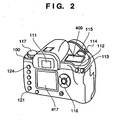
- Fig. 2 is a perspective view showing an example of the outer appearance of the digital camera according to the first embodiment.
- Fig. 3 is a longitudinal sectional view showing the digital camera having the arrangement in Fig. 2 .
- a camera main body 100 is equipped with a viewfinder observation eyepiece window 111, an AE (Auto Exposure) lock button 112, an AF (Auto Focus) measurement distance point selection button 113, the release button 114 for photographing, the electronic dial 115, a photographing mode selection dial 117, and the external display device 409.
- the electronic dial 115 is a multi-functional signal input device used to input a numerical value into the camera and switch the photographing mode in cooperation with another operation button.
- the external display device 409 is formed from a liquid crystal display device, and displays photographing conditions (e.g., shutter speed, F-number, and photographing mode) and another information.
- the back surface of the camera main body 100 is equipped with the LCD (Liquid Crystal Display) monitor device 417 which displays a sensed image, various setting windows, and the like, a monitor switch 121 for turning on/off the LCD monitor device 417, a cross-shaped switch 116, and a menu button 124.
- LCD Liquid Crystal Display
- the cross-shaped switch 116 has four buttons which are arranged up, down, right, and left, and a SET button which is arranged at the center.
- the cross-shaped switch 116 is used when the user instructs the camera to select and execute a menu item or the like displayed on the LCD monitor device 417.
- the menu button 124 is used to display a menu window for displaying various settings of the camera on the LCD monitor device 417. For example, to select and set the photographing mode, the menu button 124 is pressed, the upper, lower, right, and left buttons of the cross-shaped switch 116 are operated to select a desired mode, and the SET button is pressed while the desired mode is selected, thus completing setting.
- the menu button 124 and cross-shaped switch 116 are also used to set a dust mode (to be described later), set a display mode in the dust mode, and set an identification mark.
- the LCD monitor device 417 according to the first embodiment is of transmission type, an image cannot be checked by only driving the LCD monitor device, and the backlight illumination device 416 is always necessary on the backside of the LCD monitor device 417, as shown in Fig. 3 . As described above, the LCD monitor device 417 and backlight illumination device 416 form an image display device.
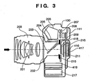
- the photographing lens 200 of the image sensing optical system is exchangeable from the camera main body 100 via a main body mount 202.
- reference numeral 201 denotes a photographing optical axis; and 203, a quick-return mirror.
- the quick-return mirror 203 is inserted in the photographing optical path, and can be moved between a position (position shown in Fig. 3 : to be referred to as an inclined position) at which the quick-return mirror 203 guides object light from the photographing lens 200 to the viewfinder optical system, and a position (to be referred to as a retract position) at which the quick-return mirror 203 retracts from the photographing optical path.
- a focusing screen 204 images object light guided from the quick-return mirror 203 to the viewfinder optical system.
- Reference numeral 205 denotes a condenser lens which improves the visibility of the viewfinder; and 206, a pentagonal roof prism which guides object light passing through the focusing screen 204 and condenser lens 205 to a viewfinder observation eyepiece lens 208 and photometry sensor 207.
- Reference numerals 209 and 210 denote a rear curtain and front curtain which form the shutter.
- the CCD 418 serving as a solid-state image sensing element arranged back is exposed to necessary light.
- a photographed image which is converted into an electrical signal of each pixel by the CCD 418 is processed by the A/D converter 423, image processing circuit 425, and the like, and recorded as image data in an external storage device.
- the CCD 418 is held by a printed board 211.
- a display substrate 215 serving as another printed board is arranged on the backside of the printed board 211.
- the LCD (Liquid Crystal Display) monitor device 417 and backlight illumination device 416 are arranged on a side of the display substrate 215 opposite to the printed board 211.
- the external storage device 419 records image data.
- Reference numeral 217 denotes a battery (portable power supply).
- the external storage device 419 and battery 217 are detachable.
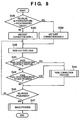
- Fig. 5 is a flowchart for explaining a dust detection process (process of detecting a pixel position at which an image error has occurred due to dust) in the digital camera according to the first embodiment. This process is performed by executing a dust detection process program stored in a nonvolatile memory (not shown) by the microcomputer 402.
- the dust detection process starts when a dust detection image is sensed.
- the camera is set with the photographing optical axis 201 of the lens 200 facing a uniform luminance plane such as the exit plane of a surface light source device.
- a dust detection light unit small-size surface light source device mounted in front of the lens is mounted on the lens 200 to prepare for dust detection.
- the first embodiment will explain the use of a normal photographing lens, but dust detection may be done by attaching to the lens mount a device which illuminates an image sensor at a uniform luminance via a diaphragm unit.
- a dust detection image has a uniform luminance.
- the microcomputer 402 sets the diaphragm. Since dust near the CCD 418 changes in imaging state depending on the F-number of the lens, dust needs to be detected at a plurality of F-numbers.
- F-number 1 predetermined F-number corresponding to the thicknesses (distance between a dust attaching position and the CCD) of a protective glass and optical filter which are arranged on the CCD is set: in this case, e.g., F8) is set (step S22).
- the microcomputer 402 causes the lens control circuit 407 to control the aperture blades of the photographing lens 200 and set the diaphragm to "F-number 1" set in step S22 (or "F-number 2" set in step S32) (step S23). At the start of the process, the diaphragm is set to the F-number set in step S22.
- photographing in the dust detection mode is executed (step S24). Details of an image sensing process routine in step S24 will be described later with reference to Fig. 4 . Photographed image data is stored in the buffer memory 424.
- the microcomputer 402 controls the lens control circuit 407 to set the diaphragm of the photographing lens 200 to a full-aperture value (step S25).
- step S26 Data which are stored in the image buffer memory 424 and correspond to the positions of pixels of a photographed image are sequentially read out to the image processing circuit 425 (step S26).
- the image processing circuit 425 compares the value of each readout pixel data with a preset threshold level (step S27). If dust attaches to the CCD 418, the quantity of light incident on a pixel corresponding to the dust attaching position decreases. By comparing each pixel data with the set threshold level, a pixel suffering an image error can be detected. If external light enters the camera main body in the dust position detection process, data obtained from a defect pixel may exceed the threshold level, and thus external light must be shielded. When no uniform luminance plane is expected in photographing, determination may be simply based on, e.g., a difference from a neighboring pixel output, instead of the threshold level of the luminance.
- the pixel position is registered in the dust position memory 427 (step S29).
- Dust position data detected using F-number 1 set in step S22 is defined as dust correction data 1.
- step S30 After all pixels are processed (step S30), it is determined whether the dust detection process has been performed for all F-numbers for detection (step S31). If an unprocessed F-number remains, the flow blanches to step S32.
- dust attaches not onto the surface of the CCD 418 but onto a protective glass or optical filter, and the imaging state changes depending on the F-number of the photographing lens.
- the F-number is close to a full-aperture value, an image is out of focus and is not influenced by attachment of small dust.
- the F-number is large, dust is clearly imaged and influences an image. For this reason, correction proper for a photographed image cannot be done unless a dust position is detected at a plurality of F-numbers and a photographed image is corrected with dust correction data corresponding to an F-number.
- step S32 another F-number (F-number 2: e.g., F22) is set (step S32).
- F-number 2 e.g., F22
- step S32 the flow then returns to step S23 to photograph an image again and perform the dust detection process (dust correction data detected at F-number 2 is defined as dust correction data 2).
- steps S23 to S31 are executed and all dust position data for a plurality of F-numbers are detected, the routine ends.
- This flowchart executes dust detection at two F-numbers, but more accurate dust correction data can be created by performing dust detection at a larger number of F-numbers. With this data, dust can be more accurately corrected.
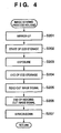
- step S24 of Fig. 5 Details of the image sensing process routine in step S24 of Fig. 5 will be described with reference to the flowchart shown in Fig. 4 .
- This process is performed by executing an image sensing process program stored in a nonvolatile memory (not shown) by the microcomputer 402.
- the microcomputer 402 When the image sensing process routine is executed, the microcomputer 402 operates the quick-return mirror 203 shown in Fig. 3 in step S201 to perform so-called mirror-up, and retracts the quick-return mirror from the photographing optical path.
- step S202 Charge storage in the CCD 418 starts in step S202, and the front curtain 210 (see Fig. 3 ) and rear curtain 209 (see Fig. 3 ) of the shutter travel to perform exposure in step S203.
- Charge storage in the CCD 418 ends in step S204.
- step S205 an image signal is read out from the CCD 418, and image data processed by the A/D converter 423 and image processing circuit 425 is temporarily stored in the buffer memory 424.
- step S206 If read of all image signals from the CCD 418 ends in step S206, the flow shifts to step S207.
- step S207 the quick-return mirror (203 in Fig. 3 ) is changed to so-called mirror-down. Then, the quick-return mirror returns to a position (inclined position) at which it guides object light to the viewfinder optical system, and a series of image sensing operations end.
- a dust correction process (dust correction process for a normally photographed image) in normal photographing in the digital camera according to the first embodiment will be explained. This process is performed by executing a dust process operation program stored in a nonvolatile memory (not shown) by the microcomputer 402.
- the microcomputer 402 executes autofocus control with the distance measurement circuit 413 and lens control circuit 407, and controls the lens 200 to an in-focus position. At the same time, the microcomputer 402 performs photometry operation by using the photometry circuit 414 to determine a TV value and F-number for control in accordance with a set photographing mode. After these processes end, the microcomputer 402 executes the image sensing process routine in Fig. 4 to sense an image. After the image is temporarily stored in the buffer memory 424, the microcomputer 402 performs the dust correction process.
- Fig. 6 is a flowchart for explaining a dust correction process in normal photographing in the digital camera according to the first embodiment.
- dust correction data for use is determined on the basis of an F-number used in photographing from a plurality of dust correction data which are stored in the dust position memory 427. More specifically, it is determined whether an F-number in photographing is equal to F-number 2 (in this case, F22) used to detect dust correction data 2 or corresponds to a smaller aperture (F-number is larger) (step S36). If the F-number in photographing is equal to F-number 2 or corresponds to a smaller aperture, the flow blanches to step S37 to determine that dust correction data 2 corresponding to F-number 2 is used. If the F-number in photographing is closer to a full-aperture value (smaller F-number) than F-number 2, the flow advances to step S38.
- F-number 2 in this case, F22
- step S38 it is determined whether the F-number in photographing is equal to F-number 1 (in this case, F8) used to detect dust correction data 1 or corresponds to a smaller aperture (F-number is larger). If the F-number in photographing is equal to F-number 1 or corresponds to a smaller aperture, the flow blanches to step S39 to determine that dust correction data 1 corresponding to F-number 1 is used. If the F-number in photographing is closer to a full-aperture value (smaller F-number) than F-number 1 in step S38, the flow advances to step S40, and it is set to correct only a pixel defect generated in the manufacture of the CCD without performing any dust correction process.
- F-number 1 in this case, F8
- the first embodiment adopts two dust correction data, and the process (steps S36 to S39) of determining dust correction data used for the dust correction process is executed at two stages.
- the process (steps S36 to S39) of determining dust correction data used for the dust correction process is executed at two stages.
- an F-number corresponding to each dust correction data and an F-number in photographing are similarly compared to determine that dust correction data which is larger than the F-number in photographing and is detected for an F-number closest to the F-number in photographing is used.
- the microcomputer 402 After dust correction data used in the dust correction process is determined by the processes in steps S36 to S40, the microcomputer 402 sequentially reads out pixel data from the image buffer memory 424 (step S42), and starts pixel defect correction. The pixel address of readout pixel data and that registered in the pixel defect position memory 426 are compared to confirm whether the pixel data corresponds to a defect pixel (step S43).
- step S44 compare the pixel address of the readout pixel data and that registered in dust correction data and confirm whether the pixel data corresponds to a pixel at which dust has been detected. If it is set in step S40 that no dust correction process is performed, the process proceeds on the assumption that no pixel address is registered in dust correction data, and the flow need not branch from step S44 to step S45.
- the image processing circuit 425 performs a correction process for the readout pixel data in step S45.
- the correction process can be done by various methods, and in the first embodiment, the pixel data is interpolated using the values of surrounding nondefective pixel data.
- the microcomputer 402, image processing circuit 425, and buffer memory 424 execute the pixel correction process in step S45, and form a dust correction process means. Since dust correction data is created for each F-number, a pixel address to be interpolated changes in accordance with the F-number in photographing. Corrected pixel data is overwritten in the buffer memory 424.
- step S46 It is confirmed whether all pixel data have been read out (step S46). If unread pixel data remains, the flow returns to step S42 to perform the above process for the unprocessed pixel data. If it is determined in step S46 that all pixels have been read, all image data of one image have undergone the interpolation process.
- the image data which are stored in the buffer memory 424 undergo an image process such as compression by the image processing circuit 425 (step S47), and written in the recording device, ending the dust correction process (and photographing process).
- the dust detection process is performed using a plurality of F-numbers, and a plurality of dust correction data corresponding to the respective F-numbers are stored.
- Optimal one of the dust correction data is used in accordance with an F-number in photographing, and a photographed image is corrected.
- an appropriate dust correction process can be achieved without generating any of the following problems: when an F-number used in dust detection is greatly different from that in photographing, dust correction is unnecessarily performed to excessively correct an image, or no necessary dust correction process is performed, resulting in an image in which dust stands out.
- a digital camera as an example of an image sensing apparatus according to the unclaimed example of the present invention will be described.
- the basic arrangement of the digital camera according to the unclaimed example is the same as that of the digital camera according to the first embodiment described above, a description of the arrangement will be omitted, and a dust detection process and dust correction process according to the unclaimed example will be explained.
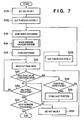
- Fig. 7 is a flowchart for explaining a dust detection process (process of detecting a pixel position at which an image error occurs due to dust) in the digital camera according to the unclaimed example.
- the same step numerals denote steps in which the same processes as those in Fig. 5 described in the first embodiment are performed, and a repetitive description thereof will be omitted.
- preparations for the dust detection process are made (for example, the camera is set with a photographing optical axis 201 of a lens 200 facing a uniform luminance plane such as the exit plane of a surface light source device).
- a microcomputer 402 sets a sensitivity given by an ISO value (read gain of a CCD 418).
- an ISO value (ISO value 1: e.g., ISO 400) is set (step S22i).
- a dust detection level (threshold level 1) corresponding to the set ISO value is set. Since noise of the CCD 418 changes depending on the ISO value, dust needs to be detected while the threshold level of dust detection is changed under a plurality of sensitivity conditions (step S22j).
- the F-number is a preset F-number (small aperture) large enough to detect dust.
- Photographing is done in the image sensing process routine described with reference to Fig. 4 (step S24).
- the diaphragm is opened to a full-aperture value (step S25).
- step S26 Data which are stored in an image buffer memory 424 and correspond to the positions of pixels are sequentially read out (step S26).
- the value of each readout image data is compared with a threshold level (first threshold level is set in step S22j) corresponding to an ISO sensitivity used in photographing (first ISO sensitivity is set in step S22i) (step S27).
- first threshold level is set in step S22j
- first ISO sensitivity is set in step S22i
- step S27 In order to discriminate dust from noise of the CCD 418, the image data value is compared with a threshold level which changes for each ISO sensitivity, thereby detecting a pixel at which an image error is generated by dust.
- step S28 If the value of the readout pixel data is smaller than the threshold level, it is confirmed whether the pixel has a pixel defect by comparing the position of the readout pixel data with the position of a defect pixel (pixel defect) in the manufacture that is stored in advance in the pixel defect position memory (step S28). Only if it is determined that the pixel does not have any pixel defect, the pixel position is registered in a dust position memory 427 (step S29).
- Dust position data detected using threshold level 1 set in step S22 is defined as dust correction data 1.
- step S31 If it is determined that read of all pixels does not end, the process returns to step S26 again to read out pixel data at the next position. If it is determined that read of all pixels ends, it is determined whether the dust detection process has been performed for all ISO sensitivities for detection (step S31). If an unprocessed ISO sensitivity remains, the flow blanches to step S32i.
- the ISO value is high (high sensitivity)
- noise is large and when a pixel at the dust position is corrected using surrounding pixels in this case, the image quality may degrade adversely.
- a dust detection level corresponding to an ISO sensitivity used in photographing is set.
- the ISO sensitivity is low and noise is hardly generated, dust is strictly detected; when the ISO sensitivity is high, dust which may become inconspicuous in noise is intentionally not detected.
- step S23 The flow returns to step S23 to photograph an image again and detect dust (dust correction data detected at ISO value 2 is used as dust correction data 2).
- steps S23 to S31 are executed and all dust position data for a plurality of ISO values are detected, the routine ends.
- This flowchart executes dust detection at two ISO values, but dust correction data can be more accurately created by performing dust detection at a larger number of ISO values. With this data, dust can be more accurately corrected.
- a dust correction process in photographing in the digital camera according to the unclaimed example will be explained. This process is performed by executing a dust process operation program stored in a nonvolatile memory (not shown) by the microcomputer 402.
- the microcomputer 402 executes autofocus control with a distance measurement circuit 413 and lens control circuit 407, and controls the lens 200 to an in-focus position. At the same time, the microcomputer 402 performs photometry operation by using a photometry circuit 414 to determine a TV value and F-number for control in accordance with a set photographing mode. After these processes end, the microcomputer 402 executes the image sensing process routine in Fig. 4 to sense an image. After the image is temporarily stored in the buffer memory 424, the microcomputer 402 performs the dust correction process.
- Fig. 8 is a flowchart for explaining a dust correction process in photographing in the digital camera according to the unclaimed example.
- the same step numerals denote steps in which the same processes as those in Fig. 6 described in the first embodiment are performed, and a repetitive description thereof will be omitted.
- dust correction data for use is determined on the basis of an ISO value used in photographing from a plurality of dust correction data which are stored in the dust position memory 427. More specifically, the ISO value in photographing is compared with a predetermined value (value between ISO value 1 and ISO value 2) (S38i).
- step S39i If the ISO value in photographing is larger than the predetermined value (represents a higher sensitivity), the flow blanches to step S39i, and it is set to perform correction by dust position data (dust correction data 2) corresponding to ISO value 2. If the ISO value in photographing is equal to or smaller than the predetermined value, the flow advances to step S40i to set dust correction data 1 (step S40i).
- the unclaimed example adopts two dust correction data, and the process (steps S38i to S40i) of determining dust correction data used for the dust correction process is executed at two stages.
- the process steps S38i to S40i
- a plurality of predetermined values to be compared are used to determine that dust correction data which is detected at an ISO value close to an ISO value in photographing is used.
- step S42 After which of dust correction data is used in the dust correction process is set in steps S38i, S39i, and S40i, data of respective pixels are sequentially read out to start pixel defect correction (step S42).
- step S43 to S45 an image correction process is done similarly to the first embodiment (steps S43 to S45). Since dust correction data is created for each ISO value, a pixel address to be interpolated changes in accordance with the ISO value in photographing. Corrected pixel data is overwritten in the buffer memory 424.
- step S46 It is confirmed whether all pixel data have been read out (step S46). If unread pixel data remains, the flow returns to step S42 to perform the above process for the unprocessed pixel data. If it is determined in step S46 that all pixels have been read, all image data of one image have undergone the interpolation process.
- the image data which are stored in the buffer memory 424 undergo an image process such as compression by an image processing circuit 425 (step S47), and written in the recording device, ending the dust correction process (and photographing process).
- the dust detection process is performed using a plurality of ISO values, and a plurality of dust correction data corresponding to the respective ISO values are stored.
- Optimal one of the dust correction data is used in accordance with an ISO value in photographing, and a photographed image is corrected.
- the unclaimed example can, therefore, prevent erroneous detection of CCD noise as dust upon photographing at a large ISO value, or a failure in detecting dust upon photographing at a small ISO value.
- the first embodiment and the unclaimed example can also be combined.
- a dust detection process is performed at combinations of ISO values and F-numbers, and dust correction data is obtained for each combination.
- Dust correction data used in the dust correction process suffices to be data detected for a combination closest to a combination of an F-number and ISO value in photographing.
Landscapes
- Engineering & Computer Science (AREA)
- Multimedia (AREA)
- Signal Processing (AREA)
- Studio Devices (AREA)
- Transforming Light Signals Into Electric Signals (AREA)
Description
- The present invention relates to an image sensing apparatus which senses an image by using an image sensor such as a CCD or CMOS, and a control method therefor.
- Recently, many image sensing apparatuses (e.g., a digital camera and digital video camera) which record an image as data by using an image sensor such as a CCD have hit the market. A digital camera does not require any photographic film which has conventionally been used as a recording medium. Instead, the digital camera records an image as data on a data recording medium such as a semiconductor memory card or hard disk device. Unlike the film, these data recording media enable repetitive write and erase conveniently, and can reduce the cost of consumables.
- A digital camera is generally equipped with an LCD monitor device capable of displaying a photographed image on request, and a removable large-capacity storage device.
- By using the digital camera having these two devices, a film serving as a recording medium which has conventionally been used as a consumable need not be used, and a photographed image can be displayed and confirmed on the LCD monitor device at once. The user can erase unsatisfactory image data on the moment, or if necessary, photograph an object again on site. Compared to a photograph using a photographic film, the photographing efficiency significantly rises.
- With this convenience and technical innovation for a larger number of pixels of an image sensor, the utilization of digital cameras is becoming wider. These days, lens exchangeable type digital cameras such as a single-lens reflex digital camera are also available.
- Unlike a film camera in which the film is transported every photographing, a digital camera takes a picture by always using the same image sensor. Dust and mote (to be generally referred to as "dust" hereinafter), which attach on an image sensor, an image sensor protective glass fixed to the image sensor, the surface of an optical filter or the like, and an optical system (to be referred to as optical system components of the image sensor at once hereinafter), stay there unless they are removed. At the position at which dust attaches, dust shields light to inhibit photographing, degrading the quality of a photographed image.
- In not only a digital camera but also a camera using a photographic film, if dust exists on a film, it is also photographed. However, the film is transported every frame, and the same dust is hardly sensed successive frames.
- To the contrary, the image sensor of the digital camera is fixed and not transported, and a common image sensor is used for photographing. Once dust attaches to the optical system component of the image sensor, the same dust is sensed in many frames (photographed images). Especially in a lens exchangeable type digital camera, dust readily attaches in exchanging a lens.
- The photographer must always be careful about attachment of dust to the optical system component of the image sensor, and spends much effort on checking and cleaning dust. In particular, since the image sensor is placed relatively deep in the camera, cleaning the sensor and confirmation of dust are not easy. In cleaning, dust may attach adversely.
- Dust readily enters the lens exchangeable type digital camera during lens exchange. In addition, most of lens exchangeable type digital cameras have a focal-plane shutter in front of the image sensor, and dust easily attach on the optical system component of the image sensor.
- In an image reading apparatus such as a film scanner, a technique to detect dust on a document table or a film document from a read image and correct the image is known (see, e.g., Japanese Patent Laid-Open No.
2003-344953 - Since dust readily attaches on the optical system component of the image sensor in the lens exchangeable type digital camera owing to its mechanism, it is important to detect attached dust, how to process detected dust, and photograph an image free from any influence of dust. If dust is left unprocessed, dust is directly sensed into an image. Dust correction at an unnecessary portion owing to a detection error of the dust position or an excessive dust process degrades an image.
-
US 2002/093577 Al teaches that an all-white reference subject is imaged by a CCD and image data representing the reference subject is obtained. The position of any dust on the reference subject represented by the reference-subject image data is detected by a dust position detector. Address data representing the position of the dust is stored in a memory that stores dust address data. When the user images a subject, image data obtained by such imaging is input to a dust correction circuit. The dust address data is read from the memory and the image at the position represented by this dust address data is eliminated from the image of the subject by reason of the fact that the image at this position is that of dust. - The present invention has been made to overcome the conventional drawbacks, and has as its object to provide an image sensing apparatus capable of suppressing the influence of dust on a photographed image even if dust attaches to an image sensor, a protective glass fixed to the image sensor, or a filter, and a control method therefor.
- Accordingly, there is provided an image sensing apparatus as set out in
independent claim 1, and a method of controlling an image sensing apparatus as set out in independent claim 6. - Advantageous developments are defined in the dependent claims.
- With this arrangement, the present invention can suppress the influence of dust on a photographed image even if dust attaches to an image sensor, a protective glass fixed to the image sensor, or a filter.
- Other objects and advantages besides those discussed above shall be apparent to those skilled in the art from the description of a preferred embodiment of the invention which follows. In the description, reference is made to accompanying drawings, which form a part thereof, and which illustrate an example of the various embodiments of the invention. Such example, however, is not exhaustive of the various embodiments of the invention, and therefore reference is made to the claims which follow the description for determining the scope of the invention.
- The accompanying drawings, which are incorporated in and constitute a part of the specification, illustrate embodiments of the invention and, together with the description, serve to explain the principles of the invention.
-
Fig. 1 is a block diagram showing an example of the circuit configuration of a single-lens reflex digital camera as an example of a lens exchangeable type image sensing apparatus according to an embodiment of the present invention; -
Fig. 2 is a perspective view showing an example of the outer appearance of the digital camera according to the embodiment; -
Fig. 3 is a longitudinal sectional view showing the internal structure of the digital camera according to the embodiment; -
Fig. 4 is a flowchart for explaining details of an image sensing process routine in step S24 ofFig. 5 ; -
Fig. 5 is a flowchart for explaining a dust detection process in a digital camera according to the first embodiment; -
Fig. 6 is a flowchart for explaining a dust correction process in the digital camera according to the first embodiment; -
Fig. 7 is a flowchart for explaining a dust detection process in a digital camera according to an unclaimed example ; and -
Fig. 8 is a flowchart for explaining a dust correction process in the digital camera according to the unclaimed example. - Preferred embodiments of the present invention will now be described in detail in accordance with the accompanying drawings.
-
Fig. 1 is a block diagram showing an example of the circuit configuration of a lens exchangeable type digital camera as an example of an image sensing apparatus according to the first embodiment of the present invention. InFig. 1 , amicrocomputer 402 controls operation of the whole camera, including a process for image data output from aCCD 418 serving as an example of an image sensor, and display control of anLCD monitor device 417. - When a release button 114 (see
Fig. 2 ) is pressed halfway, a switch (SW1) 405 is turned on (ON), and the digital camera prepares for photographing in response to ON operation of the switch (SW1) 405. When therelease button 114 is pressed fully, a switch (SW2) 406 is turned on (ON), and the digital camera starts photographing in response to ON operation of the switch (SW2) 406. - A
lens control circuit 407 controls communication with a photographing lens 200 (seeFig. 3 ), driving of the photographinglens 200 in AF (Auto Focus), and driving of an aperture blade. - In
Fig. 1 , an externaldisplay control circuit 408 controls an external display device (OLC) 409 and the display device (not shown) of the viewfinder. Aswitch sensing circuit 410 sends signals to themicrocomputer 402 from many switches including an electronic dial 411 (115 inFig. 2 ) attached to the camera. - A flash emission/
dimming control circuit 412 is grounded via anX contact 412a, and controls an external flash. Adistance measurement circuit 413 detects the defocus amount of an object for AF (Auto Focus). Aphotometry circuit 414 measures the brightness of an object. - A
shutter control circuit 415 controls the shutter, and performs correct exposure of aCCD 418. TheLCD monitor device 417 and abacklight illumination device 416 form an image display device. Astorage device 419 is, e.g., a hard disk drive or semiconductor memory card reader/writer. - The
microcomputer 402 is connected to an A/D converter 423, animage buffer memory 424, animage processing circuit 425 which is formed from a DSP and the like, a pixeldefect position memory 426 which stores the presence of a defect at a predetermined pixel itself in the CCD, and adust position memory 427 which stores a pixel position in theCCD 418 at which an image error has occurred owing to dust. The pixeldefect position memory 426 anddust position memory 427 preferably use nonvolatile memories. The pixeldefect position memory 426 anddust position memory 427 may use different address areas in the same memory space. -
Fig. 2 is a perspective view showing an example of the outer appearance of the digital camera according to the first embodiment.Fig. 3 is a longitudinal sectional view showing the digital camera having the arrangement inFig. 2 . - In
Figs. 2 and3 , the top of a cameramain body 100 is equipped with a viewfinderobservation eyepiece window 111, an AE (Auto Exposure)lock button 112, an AF (Auto Focus) measurement distancepoint selection button 113, therelease button 114 for photographing, theelectronic dial 115, a photographingmode selection dial 117, and theexternal display device 409. Theelectronic dial 115 is a multi-functional signal input device used to input a numerical value into the camera and switch the photographing mode in cooperation with another operation button. Theexternal display device 409 is formed from a liquid crystal display device, and displays photographing conditions (e.g., shutter speed, F-number, and photographing mode) and another information. - The back surface of the camera
main body 100 is equipped with the LCD (Liquid Crystal Display)monitor device 417 which displays a sensed image, various setting windows, and the like, amonitor switch 121 for turning on/off theLCD monitor device 417, across-shaped switch 116, and amenu button 124. - The
cross-shaped switch 116 has four buttons which are arranged up, down, right, and left, and a SET button which is arranged at the center. Thecross-shaped switch 116 is used when the user instructs the camera to select and execute a menu item or the like displayed on theLCD monitor device 417. - The
menu button 124 is used to display a menu window for displaying various settings of the camera on theLCD monitor device 417. For example, to select and set the photographing mode, themenu button 124 is pressed, the upper, lower, right, and left buttons of thecross-shaped switch 116 are operated to select a desired mode, and the SET button is pressed while the desired mode is selected, thus completing setting. Themenu button 124 andcross-shaped switch 116 are also used to set a dust mode (to be described later), set a display mode in the dust mode, and set an identification mark. - Since the
LCD monitor device 417 according to the first embodiment is of transmission type, an image cannot be checked by only driving the LCD monitor device, and thebacklight illumination device 416 is always necessary on the backside of theLCD monitor device 417, as shown inFig. 3 . As described above, theLCD monitor device 417 andbacklight illumination device 416 form an image display device. - As shown in
Fig. 3 , the photographinglens 200 of the image sensing optical system is exchangeable from the cameramain body 100 via amain body mount 202. InFig. 3 ,reference numeral 201 denotes a photographing optical axis; and 203, a quick-return mirror. - The quick-
return mirror 203 is inserted in the photographing optical path, and can be moved between a position (position shown inFig. 3 : to be referred to as an inclined position) at which the quick-return mirror 203 guides object light from the photographinglens 200 to the viewfinder optical system, and a position (to be referred to as a retract position) at which the quick-return mirror 203 retracts from the photographing optical path. - In
Fig. 3 , a focusingscreen 204 images object light guided from the quick-return mirror 203 to the viewfinder optical system.Reference numeral 205 denotes a condenser lens which improves the visibility of the viewfinder; and 206, a pentagonal roof prism which guides object light passing through the focusingscreen 204 andcondenser lens 205 to a viewfinderobservation eyepiece lens 208 andphotometry sensor 207. -
Reference numerals rear curtain 209 andfront curtain 210, theCCD 418 serving as a solid-state image sensing element arranged back is exposed to necessary light. A photographed image which is converted into an electrical signal of each pixel by theCCD 418 is processed by the A/D converter 423,image processing circuit 425, and the like, and recorded as image data in an external storage device. - The
CCD 418 is held by a printedboard 211. Adisplay substrate 215 serving as another printed board is arranged on the backside of the printedboard 211. The LCD (Liquid Crystal Display)monitor device 417 andbacklight illumination device 416 are arranged on a side of thedisplay substrate 215 opposite to the printedboard 211. - The
external storage device 419 records image data.Reference numeral 217 denotes a battery (portable power supply). Theexternal storage device 419 andbattery 217 are detachable. -
Fig. 5 is a flowchart for explaining a dust detection process (process of detecting a pixel position at which an image error has occurred due to dust) in the digital camera according to the first embodiment. This process is performed by executing a dust detection process program stored in a nonvolatile memory (not shown) by themicrocomputer 402. - The dust detection process starts when a dust detection image is sensed. In the dust detection process, the camera is set with the photographing
optical axis 201 of thelens 200 facing a uniform luminance plane such as the exit plane of a surface light source device. Alternatively, a dust detection light unit (small-size surface light source device mounted in front of the lens) is mounted on thelens 200 to prepare for dust detection. - The first embodiment will explain the use of a normal photographing lens, but dust detection may be done by attaching to the lens mount a device which illuminates an image sensor at a uniform luminance via a diaphragm unit. In the first embodiment, a dust detection image has a uniform luminance.
- After the end of preparations, if the start of the dust detection process is designated with, e.g., the
cross-shaped switch 116, themicrocomputer 402 sets the diaphragm. Since dust near theCCD 418 changes in imaging state depending on the F-number of the lens, dust needs to be detected at a plurality of F-numbers. First, F-number 1 (predetermined F-number corresponding to the thicknesses (distance between a dust attaching position and the CCD) of a protective glass and optical filter which are arranged on the CCD is set: in this case, e.g., F8) is set (step S22). - The
microcomputer 402 causes thelens control circuit 407 to control the aperture blades of the photographinglens 200 and set the diaphragm to "F-number 1" set in step S22 (or "F-number 2" set in step S32) (step S23). At the start of the process, the diaphragm is set to the F-number set in step S22. - After the diaphragm of the photographing lens is set, photographing in the dust detection mode is executed (step S24). Details of an image sensing process routine in step S24 will be described later with reference to
Fig. 4 . Photographed image data is stored in thebuffer memory 424. - After the end of photographing, the
microcomputer 402 controls thelens control circuit 407 to set the diaphragm of the photographinglens 200 to a full-aperture value (step S25). - Data which are stored in the
image buffer memory 424 and correspond to the positions of pixels of a photographed image are sequentially read out to the image processing circuit 425 (step S26). Theimage processing circuit 425 compares the value of each readout pixel data with a preset threshold level (step S27). If dust attaches to theCCD 418, the quantity of light incident on a pixel corresponding to the dust attaching position decreases. By comparing each pixel data with the set threshold level, a pixel suffering an image error can be detected. If external light enters the camera main body in the dust position detection process, data obtained from a defect pixel may exceed the threshold level, and thus external light must be shielded. When no uniform luminance plane is expected in photographing, determination may be simply based on, e.g., a difference from a neighboring pixel output, instead of the threshold level of the luminance. - If the value of the readout pixel data is smaller than the threshold level, it is confirmed whether the pixel has a pixel defect by comparing the position of the readout pixel data with the position of a defect pixel (pixel defect) in the manufacture that is stored in advance in the pixel defect position memory (step S28). Only if it is determined that the pixel does not have any pixel defect, the pixel position is registered in the dust position memory 427 (step S29).
- Dust position data detected using F-
number 1 set in step S22 is defined asdust correction data 1. - The same determination process (steps S26 to S29) is performed for all pixels. After all pixels are processed (step S30), it is determined whether the dust detection process has been performed for all F-numbers for detection (step S31). If an unprocessed F-number remains, the flow blanches to step S32.
- In general, dust attaches not onto the surface of the
CCD 418 but onto a protective glass or optical filter, and the imaging state changes depending on the F-number of the photographing lens. When the F-number is close to a full-aperture value, an image is out of focus and is not influenced by attachment of small dust. To the contrary, if the F-number is large, dust is clearly imaged and influences an image. For this reason, correction proper for a photographed image cannot be done unless a dust position is detected at a plurality of F-numbers and a photographed image is corrected with dust correction data corresponding to an F-number. - That is, when dust correction data which is obtained on the basis of an image photographed at a large F-number with a large depth of field is used for an image which is photographed at a small F-number close to a full-aperture value with a shallow depth of field, a correction process is done even for a portion (which is originally out of focus) which need not be corrected in practice. In contrast, when dust correction data which is photographed at an F-number close to a full-aperture value is used, dust correction data for dust which is sensed in image data photographed at a large F-number cannot be obtained, and no necessary correction process is performed. In this manner, when an F-number used to generate dust correction data and an F-number in photographing are different, a portion free from any influence of dust is excessively corrected, or a portion having dust is not corrected.
- To prevent this, another F-number (F-number 2: e.g., F22) is set (step S32). The flow then returns to step S23 to photograph an image again and perform the dust detection process (dust correction data detected at F-
number 2 is defined as dust correction data 2). - After steps S23 to S31 are executed and all dust position data for a plurality of F-numbers are detected, the routine ends. This flowchart executes dust detection at two F-numbers, but more accurate dust correction data can be created by performing dust detection at a larger number of F-numbers. With this data, dust can be more accurately corrected.
- Details of the image sensing process routine in step S24 of
Fig. 5 will be described with reference to the flowchart shown inFig. 4 . This process is performed by executing an image sensing process program stored in a nonvolatile memory (not shown) by themicrocomputer 402. - When the image sensing process routine is executed, the
microcomputer 402 operates the quick-return mirror 203 shown inFig. 3 in step S201 to perform so-called mirror-up, and retracts the quick-return mirror from the photographing optical path. - Charge storage in the
CCD 418 starts in step S202, and the front curtain 210 (seeFig. 3 ) and rear curtain 209 (seeFig. 3 ) of the shutter travel to perform exposure in step S203. Charge storage in the CCD 418 (seeFig. 3 ) ends in step S204. In step S205, an image signal is read out from theCCD 418, and image data processed by the A/D converter 423 andimage processing circuit 425 is temporarily stored in thebuffer memory 424. - If read of all image signals from the
CCD 418 ends in step S206, the flow shifts to step S207. In step S207, the quick-return mirror (203 inFig. 3 ) is changed to so-called mirror-down. Then, the quick-return mirror returns to a position (inclined position) at which it guides object light to the viewfinder optical system, and a series of image sensing operations end. - A dust correction process (dust correction process for a normally photographed image) in normal photographing in the digital camera according to the first embodiment will be explained. This process is performed by executing a dust process operation program stored in a nonvolatile memory (not shown) by the
microcomputer 402. - Assume that the above-mentioned
dust correction data dust position memory 427 prior to photographing. The photographer achieves desired photographing preparation operation by using the photographingmode dial 117,menu switch 124,electronic dial 115, and the like, and presses therelease button 114 halfway (the switch (SW1) 405 is turned on), starting photographing. - The
microcomputer 402 executes autofocus control with thedistance measurement circuit 413 andlens control circuit 407, and controls thelens 200 to an in-focus position. At the same time, themicrocomputer 402 performs photometry operation by using thephotometry circuit 414 to determine a TV value and F-number for control in accordance with a set photographing mode. After these processes end, themicrocomputer 402 executes the image sensing process routine inFig. 4 to sense an image. After the image is temporarily stored in thebuffer memory 424, themicrocomputer 402 performs the dust correction process. -
Fig. 6 is a flowchart for explaining a dust correction process in normal photographing in the digital camera according to the first embodiment. - In the dust correction process, dust correction data for use is determined on the basis of an F-number used in photographing from a plurality of dust correction data which are stored in the
dust position memory 427. More specifically, it is determined whether an F-number in photographing is equal to F-number 2 (in this case, F22) used to detectdust correction data 2 or corresponds to a smaller aperture (F-number is larger) (step S36). If the F-number in photographing is equal to F-number 2 or corresponds to a smaller aperture, the flow blanches to step S37 to determine thatdust correction data 2 corresponding to F-number 2 is used. If the F-number in photographing is closer to a full-aperture value (smaller F-number) than F-number 2, the flow advances to step S38. - In step S38, it is determined whether the F-number in photographing is equal to F-number 1 (in this case, F8) used to detect
dust correction data 1 or corresponds to a smaller aperture (F-number is larger). If the F-number in photographing is equal to F-number 1 or corresponds to a smaller aperture, the flow blanches to step S39 to determine thatdust correction data 1 corresponding to F-number 1 is used. If the F-number in photographing is closer to a full-aperture value (smaller F-number) than F-number 1 in step S38, the flow advances to step S40, and it is set to correct only a pixel defect generated in the manufacture of the CCD without performing any dust correction process. - Note that the first embodiment adopts two dust correction data, and the process (steps S36 to S39) of determining dust correction data used for the dust correction process is executed at two stages. When three or more dust correction data are prepared, an F-number corresponding to each dust correction data and an F-number in photographing are similarly compared to determine that dust correction data which is larger than the F-number in photographing and is detected for an F-number closest to the F-number in photographing is used.
- After dust correction data used in the dust correction process is determined by the processes in steps S36 to S40, the
microcomputer 402 sequentially reads out pixel data from the image buffer memory 424 (step S42), and starts pixel defect correction. The pixel address of readout pixel data and that registered in the pixeldefect position memory 426 are compared to confirm whether the pixel data corresponds to a defect pixel (step S43). - If the pixel data does not correspond to a defect pixel, the flow advances to step S44 to compare the pixel address of the readout pixel data and that registered in dust correction data and confirm whether the pixel data corresponds to a pixel at which dust has been detected. If it is set in step S40 that no dust correction process is performed, the process proceeds on the assumption that no pixel address is registered in dust correction data, and the flow need not branch from step S44 to step S45.
- If the pixel address of the readout pixel data coincides with the address of a defect pixel or a pixel at which dust has been detected in step S43 or S44, the
image processing circuit 425 performs a correction process for the readout pixel data in step S45. The correction process can be done by various methods, and in the first embodiment, the pixel data is interpolated using the values of surrounding nondefective pixel data. - In this way, according to the first embodiment, the
microcomputer 402,image processing circuit 425, andbuffer memory 424 execute the pixel correction process in step S45, and form a dust correction process means. Since dust correction data is created for each F-number, a pixel address to be interpolated changes in accordance with the F-number in photographing. Corrected pixel data is overwritten in thebuffer memory 424. - It is confirmed whether all pixel data have been read out (step S46). If unread pixel data remains, the flow returns to step S42 to perform the above process for the unprocessed pixel data. If it is determined in step S46 that all pixels have been read, all image data of one image have undergone the interpolation process. The image data which are stored in the
buffer memory 424 undergo an image process such as compression by the image processing circuit 425 (step S47), and written in the recording device, ending the dust correction process (and photographing process). - As described above, according to the first embodiment, the dust detection process is performed using a plurality of F-numbers, and a plurality of dust correction data corresponding to the respective F-numbers are stored. Optimal one of the dust correction data is used in accordance with an F-number in photographing, and a photographed image is corrected. As a result, an appropriate dust correction process can be achieved without generating any of the following problems: when an F-number used in dust detection is greatly different from that in photographing, dust correction is unnecessarily performed to excessively correct an image, or no necessary dust correction process is performed, resulting in an image in which dust stands out.
- A digital camera as an example of an image sensing apparatus according to the unclaimed example of the present invention will be described. The basic arrangement of the digital camera according to the unclaimed example is the same as that of the digital camera according to the first embodiment described above, a description of the arrangement will be omitted, and a dust detection process and dust correction process according to the unclaimed example will be explained.
-
Fig. 7 is a flowchart for explaining a dust detection process (process of detecting a pixel position at which an image error occurs due to dust) in the digital camera according to the unclaimed example. InFig. 7 , the same step numerals denote steps in which the same processes as those inFig. 5 described in the first embodiment are performed, and a repetitive description thereof will be omitted. - Similar to the first embodiment, preparations for the dust detection process are made (for example, the camera is set with a photographing
optical axis 201 of alens 200 facing a uniform luminance plane such as the exit plane of a surface light source device). - After the end of preparations, if the start of the dust detection process is designated with, e.g., a
cross-shaped switch 116, amicrocomputer 402 sets a sensitivity given by an ISO value (read gain of a CCD 418). First, an ISO value (ISO value 1: e.g., ISO 400) is set (step S22i). - A dust detection level (threshold level 1) corresponding to the set ISO value is set. Since noise of the
CCD 418 changes depending on the ISO value, dust needs to be detected while the threshold level of dust detection is changed under a plurality of sensitivity conditions (step S22j). - Operations from steps S23 to S31 are the same as that in
Fig. 5 , and only the main point will be described. - After that, a photographing lens is stopped down (step S23). At this time, the F-number is a preset F-number (small aperture) large enough to detect dust.
- Photographing is done in the image sensing process routine described with reference to
Fig. 4 (step S24). - The diaphragm is opened to a full-aperture value (step S25).
- Data which are stored in an
image buffer memory 424 and correspond to the positions of pixels are sequentially read out (step S26). The value of each readout image data is compared with a threshold level (first threshold level is set in step S22j) corresponding to an ISO sensitivity used in photographing (first ISO sensitivity is set in step S22i) (step S27). In order to discriminate dust from noise of theCCD 418, the image data value is compared with a threshold level which changes for each ISO sensitivity, thereby detecting a pixel at which an image error is generated by dust. - If the value of the readout pixel data is smaller than the threshold level, it is confirmed whether the pixel has a pixel defect by comparing the position of the readout pixel data with the position of a defect pixel (pixel defect) in the manufacture that is stored in advance in the pixel defect position memory (step S28). Only if it is determined that the pixel does not have any pixel defect, the pixel position is registered in a dust position memory 427 (step S29).
- Dust position data detected using
threshold level 1 set in step S22 is defined asdust correction data 1. - It is confirmed whether all pixels have been read out (step S30).
- If it is determined that read of all pixels does not end, the process returns to step S26 again to read out pixel data at the next position. If it is determined that read of all pixels ends, it is determined whether the dust detection process has been performed for all ISO sensitivities for detection (step S31). If an unprocessed ISO sensitivity remains, the flow blanches to step S32i.
- If the ISO value is high (high sensitivity), noise is large and when a pixel at the dust position is corrected using surrounding pixels in this case, the image quality may degrade adversely. To prevent this, a dust detection level corresponding to an ISO sensitivity used in photographing is set. When the ISO sensitivity is low and noise is hardly generated, dust is strictly detected; when the ISO sensitivity is high, dust which may become inconspicuous in noise is intentionally not detected.
- After that, another ISO value (ISO value 2: e.g., ISO = 1600) is set (step S32i), and a corresponding dust detection level (threshold level 2) is set (step S32j).
- The flow returns to step S23 to photograph an image again and detect dust (dust correction data detected at
ISO value 2 is used as dust correction data 2). - After steps S23 to S31 are executed and all dust position data for a plurality of ISO values are detected, the routine ends. This flowchart executes dust detection at two ISO values, but dust correction data can be more accurately created by performing dust detection at a larger number of ISO values. With this data, dust can be more accurately corrected.
- A dust correction process in photographing in the digital camera according to the unclaimed example will be explained. This process is performed by executing a dust process operation program stored in a nonvolatile memory (not shown) by the
microcomputer 402. - Assume that the above-mentioned
dust correction data dust position memory 427 prior to photographing. The photographer achieves desired photographing preparation operation by using a photographingmode dial 117,menu switch 124,electronic dial 115, and the like, and presses arelease button 114 halfway (a switch (SW1) 405 is turned on), starting photographing. - The
microcomputer 402 executes autofocus control with adistance measurement circuit 413 andlens control circuit 407, and controls thelens 200 to an in-focus position. At the same time, themicrocomputer 402 performs photometry operation by using aphotometry circuit 414 to determine a TV value and F-number for control in accordance with a set photographing mode. After these processes end, themicrocomputer 402 executes the image sensing process routine inFig. 4 to sense an image. After the image is temporarily stored in thebuffer memory 424, themicrocomputer 402 performs the dust correction process. -
Fig. 8 is a flowchart for explaining a dust correction process in photographing in the digital camera according to the unclaimed example. InFig. 8 , the same step numerals denote steps in which the same processes as those inFig. 6 described in the first embodiment are performed, and a repetitive description thereof will be omitted. - In the dust correction process, dust correction data for use is determined on the basis of an ISO value used in photographing from a plurality of dust correction data which are stored in the
dust position memory 427. More specifically, the ISO value in photographing is compared with a predetermined value (value betweenISO value 1 and ISO value 2) (S38i). - If the ISO value in photographing is larger than the predetermined value (represents a higher sensitivity), the flow blanches to step S39i, and it is set to perform correction by dust position data (dust correction data 2) corresponding to
ISO value 2. If the ISO value in photographing is equal to or smaller than the predetermined value, the flow advances to step S40i to set dust correction data 1 (step S40i). - Similar to the first embodiment, the unclaimed example adopts two dust correction data, and the process (steps S38i to S40i) of determining dust correction data used for the dust correction process is executed at two stages. When three or more dust correction data are prepared, a plurality of predetermined values to be compared are used to determine that dust correction data which is detected at an ISO value close to an ISO value in photographing is used.
- After which of dust correction data is used in the dust correction process is set in steps S38i, S39i, and S40i, data of respective pixels are sequentially read out to start pixel defect correction (step S42).
- Thereafter, an image correction process is done similarly to the first embodiment (steps S43 to S45). Since dust correction data is created for each ISO value, a pixel address to be interpolated changes in accordance with the ISO value in photographing. Corrected pixel data is overwritten in the
buffer memory 424. - It is confirmed whether all pixel data have been read out (step S46). If unread pixel data remains, the flow returns to step S42 to perform the above process for the unprocessed pixel data. If it is determined in step S46 that all pixels have been read, all image data of one image have undergone the interpolation process. The image data which are stored in the
buffer memory 424 undergo an image process such as compression by an image processing circuit 425 (step S47), and written in the recording device, ending the dust correction process (and photographing process). - As described above, according to the unclaimed example, the dust detection process is performed using a plurality of ISO values, and a plurality of dust correction data corresponding to the respective ISO values are stored. Optimal one of the dust correction data is used in accordance with an ISO value in photographing, and a photographed image is corrected. The unclaimed example can, therefore, prevent erroneous detection of CCD noise as dust upon photographing at a large ISO value, or a failure in detecting dust upon photographing at a small ISO value.
- The first embodiment and the unclaimed example can also be combined. In this case, a dust detection process is performed at combinations of ISO values and F-numbers, and dust correction data is obtained for each combination. Dust correction data used in the dust correction process suffices to be data detected for a combination closest to a combination of an F-number and ISO value in photographing.
- The above-described embodiments have described only a case wherein the present invention is applied to a digital camera. However, the same process can also be performed in sensing a still image by a digital video camera.
Claims (7)
- An image sensing apparatus which senses an image by using an image sensor (418), the apparatus comprising:dust position detection means (402) for detecting a pixel position corresponding to dust present on the image sensor or an optical system of the image sensor from a dust detection sensed image obtained by sensing a dust detection image; andcorrection means (402) for performing a correction process for pixel data at the pixel position corresponding to the dust among the pixel data which form a normally sensed image obtained by normal image sensing,wherein said dust position detection means (402) detects pixel positions corresponding to the dust for each of a plurality of dust detection sensed images, which are sensed with different F-numbers, and stores the respective detected pixel positions as a plurality of dust correction data corresponding to the respective F-numbers,characterized bydetermination means (402) for determining whether the correction process should be performed and determining which one of the plurality of dust correction data is to be used for performing the correction process by comparing an F-number used for sensing the normally sensed image with the respective F-numbers used for sensing the dust detection sensed images,wherein if the F-number used for sensing the normally sensed image is equal to or larger than the smallest F-number used for sensing the dust detection sensed images, said determination means (402) determines that the correction process should be performed, and further determines which one of the plurality of dust correction data is to be used for performing the correction process, otherwise the correction process is not performed.
- The apparatus according to claim 1, characterized in that the plurality of dust detection sensed images comprises a first dust detection sensed image and a second dust detection sensed image, wherein the second dust detection sensed image is sensed with a second F-number larger than a first F-number that is used for sensing the first dust detection sensed image, and the dust position detection means stores the respective detected pixel positions for the first dust detection sensed image and the second dust detection sensed image as a first dust correction data and a second dust correction data, and wherein
the determining means determines that the correction process should not be performed if the F-number used for sensing the normally sensed image is smaller than the first F-number;
the determination means determines that the correction process using the first dust correction data should be performed if the F-number used for sensing the normally sensed image is equal to or larger than the first F-number and is smaller than the second F-number ; and
the determination means determines that the correction process using the second dust correction data should be performed if the F-number used for sensing the normally sensed image is equal to or larger than the second F-number. - The apparatus according to claim 1 or 2, characterized by further comprising storage means (426) for storing information representing a position of a defect pixel in manufacture of the image sensor,
wherein said correction means (402) performs the correction process for pixel data which does not correspond to the position of the defect pixel and exists at the pixel position corresponding to the dust. - The apparatus according to any one of claims 1 to 3, characterized in that the correction process includes a process of interpolating data at the pixel position corresponding to the dust by surrounding nondefective pixel data.
- The apparatus according to any one of claims 1 to 4, characterized in that the image sensing apparatus includes a lens exchangeable type digital camera.
- A method of controlling an image sensing apparatus which senses an image by using an image sensor (418), the method comprising:a dust position detection step of detecting a pixel position corresponding to dust present on the image sensor or an optical system of the image sensor from a dust detection sensed image obtained by sensing a dust detection image; anda correction step of performing a correction process for pixel data at the pixel position corresponding to the dust among the pixel data which form a normally sensed image obtained by normal image sensing,wherein said dust position detection step detects pixel positions corresponding to the dust for each of a plurality of dust detection sensed images, which are sensed with different F-numbers, and stores the respective detected pixel positions as a plurality of dust correction data corresponding to the respective F-numbers,characterized bya determination step (S36, S38) for determining whether the correction process should be performed and determining which one of the plurality of dust correction data is to be used for performing the correction process by comparing an F-number used for sensing the normally sensed image with the respective F-numbers used for sensing the dust detection sensed images,wherein if the F-number used for sensing the normally sensed image is equal to or larger than the smallest F-number used for sensing the dust detection sensed images, said determination step determines that the correction process should be performed, and further determines which one of the plurality of dust correction data is to be used for performing the correction process, otherwise the correction process is not performed.
- The method according to claim 6, characterized in that the plurality of dust detection sensed images comprises a first dust detection sensed image and a second dust detection sensed image, wherein the second dust detection sensed image is sensed with a second F-number larger than a first F-number that is used for sensing the first dust detection sensed image, and the dust position detection step stores the respective detected pixel positions for the first dust detection sensed image and the second dust detection sensed image as a first dust correction data and a second dust correction data, and wherein
the determining step determines that the correction process should not be performed if the F-number used for sensing the normally sensed image is smaller than the first F-number;
the determination step determines that the correction process using the first dust correction data should be performed if the F-number used for sensing the normally sensed image is equal to or larger than the first F-number and is smaller than the second F-number; and
the determination step determines that the correction process using the second dust correction data should be performed if the F-number used for sensing the normally sensed image is equal to or larger than the second F-number.
Priority Applications (1)
| Application Number | Priority Date | Filing Date | Title |
|---|---|---|---|
| EP11192138.3A EP2445195B1 (en) | 2004-09-13 | 2005-09-09 | Image sensing apparatus and control method therefor |
Applications Claiming Priority (2)
| Application Number | Priority Date | Filing Date | Title |
|---|---|---|---|
| JP2004265932A JP4480147B2 (en) | 2004-09-13 | 2004-09-13 | Imaging apparatus and control method thereof |
| PCT/JP2005/017081 WO2006030874A1 (en) | 2004-09-13 | 2005-09-09 | Image sensing apparatus and control method therefor |
Related Child Applications (1)
| Application Number | Title | Priority Date | Filing Date |
|---|---|---|---|
| EP11192138.3 Division-Into | 2011-12-06 |
Publications (3)
| Publication Number | Publication Date |
|---|---|
| EP1792479A1 EP1792479A1 (en) | 2007-06-06 |
| EP1792479A4 EP1792479A4 (en) | 2009-11-25 |
| EP1792479B1 true EP1792479B1 (en) | 2013-03-27 |
Family
ID=36060123
Family Applications (2)
| Application Number | Title | Priority Date | Filing Date |
|---|---|---|---|
| EP11192138.3A Expired - Fee Related EP2445195B1 (en) | 2004-09-13 | 2005-09-09 | Image sensing apparatus and control method therefor |
| EP05783587A Expired - Fee Related EP1792479B1 (en) | 2004-09-13 | 2005-09-09 | Image sensing apparatus and control method therefor |
Family Applications Before (1)
| Application Number | Title | Priority Date | Filing Date |
|---|---|---|---|
| EP11192138.3A Expired - Fee Related EP2445195B1 (en) | 2004-09-13 | 2005-09-09 | Image sensing apparatus and control method therefor |
Country Status (6)
| Country | Link |
|---|---|
| US (1) | US7636114B2 (en) |
| EP (2) | EP2445195B1 (en) |
| JP (1) | JP4480147B2 (en) |
| KR (1) | KR100875940B1 (en) |
| CN (2) | CN101656841B (en) |
| WO (1) | WO2006030874A1 (en) |
Families Citing this family (27)
| Publication number | Priority date | Publication date | Assignee | Title |
|---|---|---|---|---|
| JP4480147B2 (en) * | 2004-09-13 | 2010-06-16 | キヤノン株式会社 | Imaging apparatus and control method thereof |
| JP4756950B2 (en) * | 2005-08-08 | 2011-08-24 | キヤノン株式会社 | Imaging apparatus and control method thereof |
| JP2007215151A (en) | 2006-01-12 | 2007-08-23 | Canon Inc | Imaging apparatus, control method thereof, and program |
| JP4757085B2 (en) * | 2006-04-14 | 2011-08-24 | キヤノン株式会社 | IMAGING DEVICE AND ITS CONTROL METHOD, IMAGE PROCESSING DEVICE, IMAGE PROCESSING METHOD, AND PROGRAM |
| JP2008033442A (en) * | 2006-07-26 | 2008-02-14 | Canon Inc | Image processor, its control method, and program |
| JP4771539B2 (en) | 2006-07-26 | 2011-09-14 | キヤノン株式会社 | Image processing apparatus, control method therefor, and program |
| JP4771540B2 (en) | 2006-07-26 | 2011-09-14 | キヤノン株式会社 | Image processing apparatus, control method therefor, image processing method and program |
| JP4695571B2 (en) * | 2006-09-14 | 2011-06-08 | 三星電子株式会社 | Imaging apparatus and imaging method |
| JP4799462B2 (en) * | 2007-03-27 | 2011-10-26 | キヤノン株式会社 | Image processing apparatus, control method thereof, program, storage medium, and imaging apparatus |
| JP2008258982A (en) | 2007-04-05 | 2008-10-23 | Canon Inc | Image processor, control method therefor, and program |
| ATE453114T1 (en) * | 2007-04-20 | 2010-01-15 | Sick Ag | METHOD AND DEVICE FOR OPTICAL DETECTION OF POLLUTION |
| JP4951540B2 (en) * | 2008-01-23 | 2012-06-13 | ペンタックスリコーイメージング株式会社 | Dust detection device and digital camera |
| JP5014195B2 (en) * | 2008-02-25 | 2012-08-29 | キヤノン株式会社 | Imaging apparatus, control method thereof, and program |
| JP2009249315A (en) * | 2008-04-03 | 2009-10-29 | Fujifilm Corp | Mineral absorption promoter, and iron deficiency anemia-ameliorating agent or food composition |
| JP5210091B2 (en) * | 2008-08-29 | 2013-06-12 | キヤノン株式会社 | Image processing apparatus, control method therefor, imaging apparatus, and program |
| US8243166B2 (en) * | 2009-01-20 | 2012-08-14 | Lockheed Martin Corporation | Automatic detection of blocked field-of-view in camera systems |
| JP2011078047A (en) * | 2009-10-02 | 2011-04-14 | Sanyo Electric Co Ltd | Imaging apparatus |
| GB201020530D0 (en) * | 2010-12-03 | 2011-01-19 | Optos Plc | Method of identifying anomalies in images |
| US11076113B2 (en) | 2013-09-26 | 2021-07-27 | Rosemount Inc. | Industrial process diagnostics using infrared thermal sensing |
| US10638093B2 (en) | 2013-09-26 | 2020-04-28 | Rosemount Inc. | Wireless industrial process field device with imaging |
| US10823592B2 (en) | 2013-09-26 | 2020-11-03 | Rosemount Inc. | Process device with process variable measurement using image capture device |
| EP2899692B1 (en) | 2014-01-28 | 2019-09-04 | Honda Research Institute Europe GmbH | Method, system, imaging device, movable device and program product for detecting static elements in video and image sources |
| US9349068B2 (en) * | 2014-06-05 | 2016-05-24 | Honeywell International Inc. | Detecting camera conditions to initiate camera maintenance |
| US10914635B2 (en) | 2014-09-29 | 2021-02-09 | Rosemount Inc. | Wireless industrial process monitor |
| US9854188B2 (en) * | 2015-12-16 | 2017-12-26 | Google Llc | Calibration of defective image sensor elements |
| CN106973291A (en) * | 2017-06-01 | 2017-07-21 | 信利光电股份有限公司 | A kind of camera module, electronic equipment, stain restorative procedure and system |
| CN108805881A (en) * | 2018-05-29 | 2018-11-13 | 周群 | Double layer rotating Table top type desk |
Family Cites Families (11)
| Publication number | Priority date | Publication date | Assignee | Title |
|---|---|---|---|---|
| JPH0951459A (en) * | 1995-08-03 | 1997-02-18 | Sanyo Electric Co Ltd | Video camera |
| JPH09200613A (en) * | 1996-01-19 | 1997-07-31 | Sony Corp | Defect detector for solid-stage imaging device |
| JP3785520B2 (en) * | 1997-03-19 | 2006-06-14 | コニカミノルタホールディングス株式会社 | Electronic camera |
| US6233364B1 (en) * | 1998-09-18 | 2001-05-15 | Dainippon Screen Engineering Of America Incorporated | Method and system for detecting and tagging dust and scratches in a digital image |
| TW466872B (en) * | 1998-12-02 | 2001-12-01 | Syscan Technology Shenzhen Co | Improved image sensing module for producing digital images having reduced noise |
| JP3461482B2 (en) * | 1999-02-24 | 2003-10-27 | オリンパス光学工業株式会社 | Digital camera and dust position detection method for digital camera |
| JP4167401B2 (en) * | 2001-01-12 | 2008-10-15 | 富士フイルム株式会社 | Digital camera and operation control method thereof |
| JP3863723B2 (en) * | 2001-02-09 | 2006-12-27 | ペンタックス株式会社 | Interchangeable lens electronic still camera |
| JP2003344953A (en) | 2002-05-30 | 2003-12-03 | Canon Inc | Image reader |
| JP2004265932A (en) | 2003-02-14 | 2004-09-24 | Canon Inc | Radiation imaging device |
| JP4480147B2 (en) * | 2004-09-13 | 2010-06-16 | キヤノン株式会社 | Imaging apparatus and control method thereof |
-
2004
- 2004-09-13 JP JP2004265932A patent/JP4480147B2/en not_active Expired - Fee Related
-
2005
- 2005-09-09 KR KR1020077007846A patent/KR100875940B1/en not_active IP Right Cessation
- 2005-09-09 EP EP11192138.3A patent/EP2445195B1/en not_active Expired - Fee Related
- 2005-09-09 WO PCT/JP2005/017081 patent/WO2006030874A1/en active Application Filing
- 2005-09-09 EP EP05783587A patent/EP1792479B1/en not_active Expired - Fee Related
- 2005-09-09 CN CN2009101681907A patent/CN101656841B/en not_active Expired - Fee Related
- 2005-09-09 US US10/555,023 patent/US7636114B2/en not_active Expired - Fee Related
- 2005-09-09 CN CNB2005800306247A patent/CN100550995C/en not_active Expired - Fee Related
Also Published As
| Publication number | Publication date |
|---|---|
| CN101656841A (en) | 2010-02-24 |
| CN101019419A (en) | 2007-08-15 |
| EP1792479A4 (en) | 2009-11-25 |
| CN101656841B (en) | 2011-09-21 |
| US20070030378A1 (en) | 2007-02-08 |
| JP4480147B2 (en) | 2010-06-16 |
| JP2006081122A (en) | 2006-03-23 |
| KR20070088585A (en) | 2007-08-29 |
| EP2445195B1 (en) | 2013-07-10 |
| CN100550995C (en) | 2009-10-14 |
| KR100875940B1 (en) | 2008-12-26 |
| US7636114B2 (en) | 2009-12-22 |
| EP1792479A1 (en) | 2007-06-06 |
| EP2445195A1 (en) | 2012-04-25 |
| WO2006030874A1 (en) | 2006-03-23 |
Similar Documents
| Publication | Publication Date | Title |
|---|---|---|
| EP1792479B1 (en) | Image sensing apparatus and control method therefor | |
| JP4590355B2 (en) | Image processing apparatus, image processing method, and program | |
| US6927794B2 (en) | Digital camera provided with a plurality of mounting portions to each of which a recording medium is mounted | |
| JP2007215151A (en) | Imaging apparatus, control method thereof, and program | |
| US8471935B2 (en) | Imaging apparatus having an image correction function and method for controlling the same | |
| US7532815B2 (en) | Lens unit, method of identifying characteristics thereof and method of judging deterioration thereof, and digital camera | |
| JP4532819B2 (en) | Imaging device | |
| JP2006313250A (en) | Lens-interchanging type digital camera | |
| JP4845256B2 (en) | Image processing device | |
| JP2006313978A (en) | Imaging apparatus, control method, and computer program | |
| JPH1188761A (en) | Digital camera and storage medium | |
| JP4859194B2 (en) | IMAGING DEVICE, ITS CONTROL METHOD, PROGRAM, AND STORAGE MEDIUM | |
| JP2007006024A (en) | Imaging apparatus | |
| JP3605084B2 (en) | Image data correction device, image processing device, image data correction method, program, and storage medium | |
| JP4480188B2 (en) | Imaging apparatus and control method thereof | |
| JP2001078083A (en) | Exposure time controller for electronic still camera | |
| JP2002135636A (en) | Electronic camera | |
| JP2008042348A (en) | Image processor, image processing method, imaging apparatus and program | |
| JP2010098698A (en) | Imaging apparatus, control method thereof and program | |
| JP2007101860A (en) | Imaging apparatus | |
| JP2005175961A (en) | Imaging apparatus, image sensitivity control method, shutter control method, and program | |
| JP5094571B2 (en) | Imaging apparatus, control method thereof, and program | |
| JP2006108878A (en) | Imaging apparatus | |
| JP2003092703A (en) | Electronic camera and its control method | |
| JP2005136654A (en) | Camera |
Legal Events
| Date | Code | Title | Description |
|---|---|---|---|
| PUAI | Public reference made under article 153(3) epc to a published international application that has entered the european phase |
Free format text: ORIGINAL CODE: 0009012 |
|
| 17P | Request for examination filed |
Effective date: 20070413 |
|
| AK | Designated contracting states |
Kind code of ref document: A1 Designated state(s): DE FR GB |
|
| DAX | Request for extension of the european patent (deleted) | ||
| RBV | Designated contracting states (corrected) |
Designated state(s): DE FR GB |
|
| A4 | Supplementary search report drawn up and despatched |
Effective date: 20091027 |
|
| RIC1 | Information provided on ipc code assigned before grant |
Ipc: H04N 5/335 20060101AFI20060908BHEP |
|
| 17Q | First examination report despatched |
Effective date: 20110720 |
|
| RIC1 | Information provided on ipc code assigned before grant |
Ipc: H04N 5/367 20110101ALI20120309BHEP Ipc: H04N 5/232 20060101AFI20120309BHEP |
|
| REG | Reference to a national code |
Ref country code: DE Ref legal event code: R079 Ref document number: 602005038789 Country of ref document: DE Free format text: PREVIOUS MAIN CLASS: H04N0005335000 Ipc: H04N0005217000 |
|
| GRAP | Despatch of communication of intention to grant a patent |
Free format text: ORIGINAL CODE: EPIDOSNIGR1 |
|
| RIC1 | Information provided on ipc code assigned before grant |
Ipc: H04N 5/232 20060101ALI20120906BHEP Ipc: H04N 5/217 20110101AFI20120906BHEP Ipc: H04N 5/367 20110101ALI20120906BHEP |
|
| GRAS | Grant fee paid |
Free format text: ORIGINAL CODE: EPIDOSNIGR3 |
|
| GRAA | (expected) grant |
Free format text: ORIGINAL CODE: 0009210 |
|
| AK | Designated contracting states |
Kind code of ref document: B1 Designated state(s): DE FR GB |
|
| REG | Reference to a national code |
Ref country code: GB Ref legal event code: FG4D |
|
| REG | Reference to a national code |
Ref country code: DE Ref legal event code: R096 Ref document number: 602005038789 Country of ref document: DE Effective date: 20130529 |
|
| PLBE | No opposition filed within time limit |
Free format text: ORIGINAL CODE: 0009261 |
|
| STAA | Information on the status of an ep patent application or granted ep patent |
Free format text: STATUS: NO OPPOSITION FILED WITHIN TIME LIMIT |
|
| 26N | No opposition filed |
Effective date: 20140103 |
|
| REG | Reference to a national code |
Ref country code: DE Ref legal event code: R097 Ref document number: 602005038789 Country of ref document: DE Effective date: 20140103 |
|
| REG | Reference to a national code |
Ref country code: FR Ref legal event code: ST Effective date: 20140530 |
|
| PG25 | Lapsed in a contracting state [announced via postgrant information from national office to epo] |
Ref country code: FR Free format text: LAPSE BECAUSE OF NON-PAYMENT OF DUE FEES Effective date: 20130930 |
|
| PGFP | Annual fee paid to national office [announced via postgrant information from national office to epo] |
Ref country code: DE Payment date: 20140930 Year of fee payment: 10 |
|
| PGFP | Annual fee paid to national office [announced via postgrant information from national office to epo] |
Ref country code: GB Payment date: 20140924 Year of fee payment: 10 |
|
| REG | Reference to a national code |
Ref country code: DE Ref legal event code: R119 Ref document number: 602005038789 Country of ref document: DE |
|
| GBPC | Gb: european patent ceased through non-payment of renewal fee |
Effective date: 20150909 |
|
| PG25 | Lapsed in a contracting state [announced via postgrant information from national office to epo] |
Ref country code: DE Free format text: LAPSE BECAUSE OF NON-PAYMENT OF DUE FEES Effective date: 20160401 Ref country code: GB Free format text: LAPSE BECAUSE OF NON-PAYMENT OF DUE FEES Effective date: 20150909 |