EP1756796B1 - Color display device with enhanced pixel pattern - Google Patents
Color display device with enhanced pixel pattern Download PDFInfo
- Publication number
- EP1756796B1 EP1756796B1 EP05754388.6A EP05754388A EP1756796B1 EP 1756796 B1 EP1756796 B1 EP 1756796B1 EP 05754388 A EP05754388 A EP 05754388A EP 1756796 B1 EP1756796 B1 EP 1756796B1
- Authority
- EP
- European Patent Office
- Prior art keywords
- subpixel
- subpixels
- pixel
- display
- red
- Prior art date
- Legal status (The legal status is an assumption and is not a legal conclusion. Google has not performed a legal analysis and makes no representation as to the accuracy of the status listed.)
- Active
Links
- 239000003086 colorant Substances 0.000 claims description 11
- 238000010586 diagram Methods 0.000 description 20
- 239000004973 liquid crystal related substance Substances 0.000 description 4
- 241000526960 Amaranthus acanthochiton Species 0.000 description 2
- 239000011159 matrix material Substances 0.000 description 2
- 230000000717 retained effect Effects 0.000 description 2
- 230000000007 visual effect Effects 0.000 description 2
- 230000032683 aging Effects 0.000 description 1
- 238000003491 array Methods 0.000 description 1
- 230000009286 beneficial effect Effects 0.000 description 1
- 230000001419 dependent effect Effects 0.000 description 1
- 238000013461 design Methods 0.000 description 1
- 238000011161 development Methods 0.000 description 1
- 230000018109 developmental process Effects 0.000 description 1
- 238000005516 engineering process Methods 0.000 description 1
- 238000002474 experimental method Methods 0.000 description 1
- 238000003384 imaging method Methods 0.000 description 1
- 239000000463 material Substances 0.000 description 1
- 238000000034 method Methods 0.000 description 1
- 239000000203 mixture Substances 0.000 description 1
- 230000007935 neutral effect Effects 0.000 description 1
- 230000005855 radiation Effects 0.000 description 1
- 238000011160 research Methods 0.000 description 1
- 229920006395 saturated elastomer Polymers 0.000 description 1
- 239000010409 thin film Substances 0.000 description 1
Images


Classifications
-
- G—PHYSICS
- G09—EDUCATION; CRYPTOGRAPHY; DISPLAY; ADVERTISING; SEALS
- G09G—ARRANGEMENTS OR CIRCUITS FOR CONTROL OF INDICATING DEVICES USING STATIC MEANS TO PRESENT VARIABLE INFORMATION
- G09G3/00—Control arrangements or circuits, of interest only in connection with visual indicators other than cathode-ray tubes
- G09G3/20—Control arrangements or circuits, of interest only in connection with visual indicators other than cathode-ray tubes for presentation of an assembly of a number of characters, e.g. a page, by composing the assembly by combination of individual elements arranged in a matrix no fixed position being assigned to or needed to be assigned to the individual characters or partial characters
- G09G3/22—Control arrangements or circuits, of interest only in connection with visual indicators other than cathode-ray tubes for presentation of an assembly of a number of characters, e.g. a page, by composing the assembly by combination of individual elements arranged in a matrix no fixed position being assigned to or needed to be assigned to the individual characters or partial characters using controlled light sources
- G09G3/30—Control arrangements or circuits, of interest only in connection with visual indicators other than cathode-ray tubes for presentation of an assembly of a number of characters, e.g. a page, by composing the assembly by combination of individual elements arranged in a matrix no fixed position being assigned to or needed to be assigned to the individual characters or partial characters using controlled light sources using electroluminescent panels
- G09G3/32—Control arrangements or circuits, of interest only in connection with visual indicators other than cathode-ray tubes for presentation of an assembly of a number of characters, e.g. a page, by composing the assembly by combination of individual elements arranged in a matrix no fixed position being assigned to or needed to be assigned to the individual characters or partial characters using controlled light sources using electroluminescent panels semiconductive, e.g. using light-emitting diodes [LED]
- G09G3/3208—Control arrangements or circuits, of interest only in connection with visual indicators other than cathode-ray tubes for presentation of an assembly of a number of characters, e.g. a page, by composing the assembly by combination of individual elements arranged in a matrix no fixed position being assigned to or needed to be assigned to the individual characters or partial characters using controlled light sources using electroluminescent panels semiconductive, e.g. using light-emitting diodes [LED] organic, e.g. using organic light-emitting diodes [OLED]
- G09G3/3216—Control arrangements or circuits, of interest only in connection with visual indicators other than cathode-ray tubes for presentation of an assembly of a number of characters, e.g. a page, by composing the assembly by combination of individual elements arranged in a matrix no fixed position being assigned to or needed to be assigned to the individual characters or partial characters using controlled light sources using electroluminescent panels semiconductive, e.g. using light-emitting diodes [LED] organic, e.g. using organic light-emitting diodes [OLED] using a passive matrix
-
- G—PHYSICS
- G09—EDUCATION; CRYPTOGRAPHY; DISPLAY; ADVERTISING; SEALS
- G09G—ARRANGEMENTS OR CIRCUITS FOR CONTROL OF INDICATING DEVICES USING STATIC MEANS TO PRESENT VARIABLE INFORMATION
- G09G3/00—Control arrangements or circuits, of interest only in connection with visual indicators other than cathode-ray tubes
- G09G3/20—Control arrangements or circuits, of interest only in connection with visual indicators other than cathode-ray tubes for presentation of an assembly of a number of characters, e.g. a page, by composing the assembly by combination of individual elements arranged in a matrix no fixed position being assigned to or needed to be assigned to the individual characters or partial characters
- G09G3/22—Control arrangements or circuits, of interest only in connection with visual indicators other than cathode-ray tubes for presentation of an assembly of a number of characters, e.g. a page, by composing the assembly by combination of individual elements arranged in a matrix no fixed position being assigned to or needed to be assigned to the individual characters or partial characters using controlled light sources
- G09G3/30—Control arrangements or circuits, of interest only in connection with visual indicators other than cathode-ray tubes for presentation of an assembly of a number of characters, e.g. a page, by composing the assembly by combination of individual elements arranged in a matrix no fixed position being assigned to or needed to be assigned to the individual characters or partial characters using controlled light sources using electroluminescent panels
- G09G3/32—Control arrangements or circuits, of interest only in connection with visual indicators other than cathode-ray tubes for presentation of an assembly of a number of characters, e.g. a page, by composing the assembly by combination of individual elements arranged in a matrix no fixed position being assigned to or needed to be assigned to the individual characters or partial characters using controlled light sources using electroluminescent panels semiconductive, e.g. using light-emitting diodes [LED]
- G09G3/3208—Control arrangements or circuits, of interest only in connection with visual indicators other than cathode-ray tubes for presentation of an assembly of a number of characters, e.g. a page, by composing the assembly by combination of individual elements arranged in a matrix no fixed position being assigned to or needed to be assigned to the individual characters or partial characters using controlled light sources using electroluminescent panels semiconductive, e.g. using light-emitting diodes [LED] organic, e.g. using organic light-emitting diodes [OLED]
- G09G3/3225—Control arrangements or circuits, of interest only in connection with visual indicators other than cathode-ray tubes for presentation of an assembly of a number of characters, e.g. a page, by composing the assembly by combination of individual elements arranged in a matrix no fixed position being assigned to or needed to be assigned to the individual characters or partial characters using controlled light sources using electroluminescent panels semiconductive, e.g. using light-emitting diodes [LED] organic, e.g. using organic light-emitting diodes [OLED] using an active matrix
-
- G—PHYSICS
- G09—EDUCATION; CRYPTOGRAPHY; DISPLAY; ADVERTISING; SEALS
- G09G—ARRANGEMENTS OR CIRCUITS FOR CONTROL OF INDICATING DEVICES USING STATIC MEANS TO PRESENT VARIABLE INFORMATION
- G09G5/00—Control arrangements or circuits for visual indicators common to cathode-ray tube indicators and other visual indicators
- G09G5/02—Control arrangements or circuits for visual indicators common to cathode-ray tube indicators and other visual indicators characterised by the way in which colour is displayed
-
- G—PHYSICS
- G09—EDUCATION; CRYPTOGRAPHY; DISPLAY; ADVERTISING; SEALS
- G09G—ARRANGEMENTS OR CIRCUITS FOR CONTROL OF INDICATING DEVICES USING STATIC MEANS TO PRESENT VARIABLE INFORMATION
- G09G2300/00—Aspects of the constitution of display devices
- G09G2300/04—Structural and physical details of display devices
- G09G2300/0439—Pixel structures
- G09G2300/0452—Details of colour pixel setup, e.g. pixel composed of a red, a blue and two green components
-
- G—PHYSICS
- G09—EDUCATION; CRYPTOGRAPHY; DISPLAY; ADVERTISING; SEALS
- G09G—ARRANGEMENTS OR CIRCUITS FOR CONTROL OF INDICATING DEVICES USING STATIC MEANS TO PRESENT VARIABLE INFORMATION
- G09G2320/00—Control of display operating conditions
- G09G2320/02—Improving the quality of display appearance
-
- G—PHYSICS
- G09—EDUCATION; CRYPTOGRAPHY; DISPLAY; ADVERTISING; SEALS
- G09G—ARRANGEMENTS OR CIRCUITS FOR CONTROL OF INDICATING DEVICES USING STATIC MEANS TO PRESENT VARIABLE INFORMATION
- G09G3/00—Control arrangements or circuits, of interest only in connection with visual indicators other than cathode-ray tubes
- G09G3/20—Control arrangements or circuits, of interest only in connection with visual indicators other than cathode-ray tubes for presentation of an assembly of a number of characters, e.g. a page, by composing the assembly by combination of individual elements arranged in a matrix no fixed position being assigned to or needed to be assigned to the individual characters or partial characters
- G09G3/34—Control arrangements or circuits, of interest only in connection with visual indicators other than cathode-ray tubes for presentation of an assembly of a number of characters, e.g. a page, by composing the assembly by combination of individual elements arranged in a matrix no fixed position being assigned to or needed to be assigned to the individual characters or partial characters by control of light from an independent source
- G09G3/36—Control arrangements or circuits, of interest only in connection with visual indicators other than cathode-ray tubes for presentation of an assembly of a number of characters, e.g. a page, by composing the assembly by combination of individual elements arranged in a matrix no fixed position being assigned to or needed to be assigned to the individual characters or partial characters by control of light from an independent source using liquid crystals
- G09G3/3607—Control arrangements or circuits, of interest only in connection with visual indicators other than cathode-ray tubes for presentation of an assembly of a number of characters, e.g. a page, by composing the assembly by combination of individual elements arranged in a matrix no fixed position being assigned to or needed to be assigned to the individual characters or partial characters by control of light from an independent source using liquid crystals for displaying colours or for displaying grey scales with a specific pixel layout, e.g. using sub-pixels
Definitions
- the present invention relates to color display devices and, more particularly, to arrangements of subpixel elements in such color display devices.
- US Patent Application Publication 2002/0186214A1 shows a method for saving power in an organic light emitting diode (OLED) display having pixels comprised of red, green, blue and white light emitting subpixel elements.
- the white light emitting subpixel elements are more efficient than the other colored light emitting subpixel elements and are employed to reduce the power requirements of the display.
- the red, green, blue and white light emitting subpixel elements can be illuminated to create any desired color within the gamut of the red, green, and blue light emitting subpixel elements.
- the white light emitting subpixel elements are more efficient than the red, green, or blue light emitting subpixel element it is desirable to present any neutral color by turning on only the white light emitting subpixel element within a pixel containing the four light emitting subpixel elements.
- the human eye is most sensitive to greenish yellow light and less sensitive to red and blue light. More specifically, the spatial resolution of the human visual system is driven primarily by the luminance rather than the chrominance of a signal. Since green light provides the preponderance of luminance information in typical viewing environments, the spatial resolution of the visual system during normal daylight viewing conditions is highest for green light, lower for red light, and even lower for blue light when viewing images generated by a typical color balanced image capture and display system. This fact has been used in a variety of ways to optimize the frequency response of imaging systems.
- banding artifacts i.e., the visibility of dark lines within a row or column of the pixel structure
- a pixel 22 contains red R, green G, and blue B light emitting subpixel elements. Neighboring pixels are positioned within a grid around this pixel such that they are aligned in rows and columns. As with the quad pattern this pixel pattern can exhibit banding artifacts in regions of flat pure primary colors.
- this pattern includes a similar pixel 32, having red R, green G, and blue B light emitting elements.
- this pattern reduces the visibility of banding and improves the uniform appearance in areas of constant color by shifting the alignment of the red, green, and blue subpixel elements in alternating rows.
- this pattern creates a visible jagged pattern in vertical lines containing primarily green light emitting subpixel elements as the human eye is very sensitive to offsets in light emitting subpixel elements that are high in luminance.
- EP 1 388 818 A2 discloses an apparatus having an array of subpixels of at least four different colors including two relatively higher luminous color subpixels and two relatively lower luminous color subpixels. A repeating pattern is set forth.
- JP S60-263 122 A discloses an array having multiple different colors but not arranged in repeating pattern.
- US 2004/0095521 A1 may be construed to disclose a liquid crystal display, which includes a liquid crystal panel assembly including a plurality of red, green, blue and white pixel areas, and a backlight unit placed at a side of the liquid crystal panel assembly.
- the light emitted from the backlight unit has a color coordinate (x, y) where x ranges from about 0.31 to about 0.34, and y ranges from about 0.32 to about 0.35.
- this pixel pattern will provide the enhanced power savings that is available, e.g., from a pattern containing red, green, blue and white subpixels and allow the relative sizes of the light emitting subpixel elements to be readily adjusted.
- a color display device comprising: an array of subpixels of at least four different colors, including at least two relatively higher luminous color subpixels and at least two relatively lower luminous color subpixels, wherein the relatively higher luminous color subpixels are selected from white, green, yellow or cyan subpixels, and the relatively lower luminous color subpixels are blue and red subpixels, the subpixels are arranged into groups forming at least two distinct types of pixels, each pixel type including the two relatively higher luminous color subpixels and at least one of the two relatively lower luminous color subpixels, and the pixel types are arranged in a pattern such that the relative locations of the two relatively higher luminous color subpixels in each pixel is repeated in the adjacent pixels, and the relative location of at least one of the two relatively lower luminance color subpixels is not repeated in at least one adjacent pixel, wherein the at least two relatively higher luminous color subpixels and the at least two relatively lower luminous color subpixels are four different colored subpixels.
- Various embodiments of the invention enable color display devices with improved image display quality, with both the appearance of jagged lines and the appearance of banding reduced simultaneously.
- the invention is directed towards a color display device, comprising: an array of subpixels of at least four different colors, including at least two relatively higher luminous color subpixels and at least two relatively lower luminous color subpixels, wherein the subpixels are arranged into groups forming at least two distinct types of pixels, each pixel type including the two relatively higher luminous color subpixels and at least one of the two relatively lower luminous color subpixels, and wherein the pixel types are arranged in a pattern such that the relative locations of the two relatively higher luminous color subpixels in each pixel is repeated in adjacent pixels, and the relative location of at least one of the two relatively lower luminance color subpixels is not repeated in at least one adjacent pixel.
- the relatively higher luminous color subpixels are selected from white, green, yellow or cyan subpixels
- the relatively lower luminous color subpixels are blue and red subpixels.
- subpixel elements that bear a significant portion of a display device luminance may be aligned between adjacent pixels within a pattern in accordance with the invention to avoid the appearance of jagged lines.
- subpixel elements that provide a smaller proportion of the display luminance are less likely to provide visible spatial patterns, and need not be aligned between adjacent pixels.
- the relative positions of subpixel elements that provide a smaller proportion of the display luminance may thus be distributed evenly, switching positions between adjacent pixels, and such locations may contribute to an improvement of the display image uniformity of the pattern.
- each of the two distinct pixel types employed include the two relatively lower luminous color subpixels, and the pixel types are arranged such that the relative locations of the two relatively lower luminance color subpixels are interchanged between adjacent pixels in successive rows and/or columns of pixels.
- a display panel 40 (a small portion of which is shown) according to the present invention includes a repeating array of two distinct types of pixels 42 and 44 .
- Each pixel is composed of a red R , a green G and a blue B light emitting subpixel element that define the gamut of the display and an additional subpixel element W that emits light having a color within the gamut (e.g. white).
- the white and green light emitting subpixel elements are arranged in vertical columns while the blue and red light emitting subpixel elements are separated within the pattern.
- the additional subpixel element W is preferably constructed to have a power efficiency that is higher than the power efficiency of at least one of the red R , green G , and blue B light emitting subpixel elements.
- the additional light emitting subpixel element provides a greater peak luminance contribution than the peak luminance of either the red or blue subpixel elements. It is well known that the green subpixel element also provides a greater peak luminance contribution than either the red or blue subpixel elements.
- the white W and green G light emitting subpixel elements are aligned such that the position of each of these subpixel elements is the same for each pixel within the display device 40 .
- the green 42G and 44G light emitting subpixel element is the second light emitting within each pixel.
- the white light emitting subpixel element 42W and 44W is the third light emitting subpixel element within each pixel. Since, these subpixel elements present the majority of the luminance information, positioning the white W and the green G light emitting subpixel elements in horizontal rows and vertical columns, the visibility of jagged lines are avoided within the pattern.
- red light emitting subpixel element 42R in one pixel 42 is the first light emitting subpixel element but in the second row the red light emitting subpixel element 44R is the fourth light emitting subpixel element.
- the blue light emitting subpixel element in the first pixel 42B is the fourth light emitting subpixel element but in the succeeding row, the blue light emitting subpixel element 44B is the first light emitting subpixel element.
- alternating rows of pixels in the display comprise a first pixel type wherein the subpixels are positioned in a sequence of red, green, white and blue rectangles, whose long axes are oriented vertically, and whose long axes are parallel to each other, said sequence of subpixels in said alternating rows of pixels repeating across the width of the display; and interleaving rows of pixels between the alternating rows in the display comprise a second pixel type wherein the subpixels are positioned in a sequence of blue, green, white and red rectangles, whose long axes are oriented vertically, and whose long axes are parallel to each other, the sequence of subpixels in the interleaving rows of pixels repeating across the width of the display.
- the sequences of subpixels in alternating and interleaving rows repeat across the height of the display. While the rectangular subpixels are illustrated as being of equal width and length, they may independently be selected to be of different width or length.
- the uniformity of the pattern is improved and the visibility of banding artifacts are significantly reduced.
- This arrangement of light emitting subpixel elements allows both the appearance of jagged lines and the appearance of banding to be reduced simultaneously provides an improvement in overall image quality that has been demonstrated by the present inventors to be greater than it is in patterns where the visibility of only one of these artifacts are reduced at the expense of increasing the visibility of the other.
- a display panel 50 (a small portion of which is shown) includes an alternative arrangement of light emitting subpixel elements within a repeating array of two distinct types of pixels 52 and 54 .
- This arrangement of red R , green G , blue B , and white W light emitting subpixel elements is similar to the one shown in Fig. 4 .
- the white W and green G columns of pixels are separated to provide a pattern that is more uniform in appearance.
- columns and rows of the luminance bearing light emitting subpixel elements i.e., white and green
- 52W and 54W as well as 52G and 54G are aligned in vertical columns.
- the position of the blue B and red R light emitting subpixel elements are displaced in succeeding rows.
- the red light emitting subpixel element 52R is located in the same column and above the blue light emitting subpixel element 54B .
- the blue light emitting subpixel element 52B is located in the same column and above the red light emitting subpixel element 54R .
- the sequences of subpixels in alternating and interleaving rows repeat across the height of the display.
- FIG. 6 An alternative embodiment is shown in Fig. 6 .
- This figure shows a small portion of a display panel 60 , including an alternative arrangement of light emitting subpixel elements within a repeating array.
- This figure shows two distinct types of pixels 62 and 64 .
- the white W and green G light emitting subpixel elements are located in the same location within each pixel.
- the position of the red R and blue B light emitting subpixel elements are interchanged between each vertical pair of pixels. That is, the white ( 62W and 64W ) and green ( 62G and 64G ) are located the same within pixels 62 and 64 .
- the position of the red ( 62R and 64R ) and blue ( 62B and 64B ) are interchanged in succeeding rows of pixels.
- the sequences of subpixels in alternating and interleaving rows repeat across the height of the display.
- providing a fixed position for the elements that bear the majority of the luminance information ( G and W ) avoids the visibility of jagged lines, while interchanging the location of the red and blue light emitting elements reduces the appearance of banding.
- FIG.7 An alternate embodiment of the present invention is shown in Fig.7 .
- a small portion of a display panel 70 is shown that includes four pixels. This is a departure from the quad pattern of Fig. 1 and those known previously in the art.
- the two distinct types of pixels 72 and 74 each contain green subpixels ( 72G and 74G ) and white pixels ( 72W and 74W ). These G and W subpixels are aligned with respect to the vertical axis, and are located in the same position within pixels 72 and 74 . However, as in Fig. 6 , the position of the red ( 72R and 74R ) and blue ( 72B and 74B ) subpixels are interchanged in succeeding rows of pixels.
- the sequences of subpixels in alternating and interleaving rows repeat across the height of the display.
- the interchange principle of low luminance subpixels of the present invention is used, resulting in a pattern that is better optimized to the situation where characters, pictorial detail and uniform areas must all be displayed.
- FIG. 8 Another embodiment of the present invention is shown in Fig. 8 .
- a small portion of a display panel 80 is shown that includes four pixels.
- distinct types of pixels 82 and 84 each contain high luminance subpixels 82G , 82W and 84G , 84W .
- the G and W subpixels are not aligned with respect to each other within the pixel cell, however they are seen to remain in a fixed relative position inside the pixel cell as one moves from pixel to pixel.
- the G and W maintain their overall alignment with respect to themselves, while the R and B subpixels ( 82R, 82B, 84R, 84B ) alternate positions between rows of pixels.
- the sequences of subpixels in alternating and interleaving rows repeat across the height of the display.
- the white W and green G light emitting subpixel elements are located at the same location within each pixel.
- the white ( 92W and 94W ) and green ( 92G and 94G ) light emitting subpixel elements are located at the same position within each pixel.
- each pixel contains only one of these two subpixel elements.
- the red 92R light emitting subpixel element is located in every other pixel.
- the blue 94B light emitting subpixel element is also located in every other pixel and the blue 94B light emitting subpixel element is located at the same location in pixel 94 as the red 92R light emitting subpixel element is located in pixel 92 .
- the sequences of subpixels in alternating and interleaving rows repeat across the height of the display.
- differently sized light emitting subpixel elements may be used.
- Studies conducted by the present inventors have shown that saturated colors occur less frequently than unsaturated colors in both natural and computer generated images and graphics.
- the efficiency of a display can be improved by using the additional subpixel element in the place of the gamut defining subpixel elements.
- the use of the additional subpixel element can be so high in typical applications that in order to reduce the current density in the additional subpixel element, it is useful to increase the size of the additional subpixel element.
- typical OLED materials presently in use have a relatively higher efficiency for the additional subpixel element and the green subpixel element, and a relatively lower efficiency for the red and blue subpixel elements.
- an optimized display according to the present invention may have relatively larger red, blue and additional subpixel elements, and relatively smaller green subpixel elements.
- the additional white OLED subpixel elements will be used more heavily than any of the gamut defining subpixel elements and may therefore be increased in size to reduce the current density and hence aging of the additional subpixel element.
- Text, graphic, and pictorial based applications are typically of these types.
- FIG. 10 A small portion of a display panel 100 is shown, including four pixels.
- distinct types of pixels 102 and 104 each contain green and white subpixel elements ( 102G , 104G and 102W , 104W ) that are located in the same position, and are the same size, within each pixel.
- 102 contains a red subpixel 102R , but not a blue subpixel
- 104 contains a blue subpixel 104B , but not a red subpixel.
- the size of the red and blue subpixels is the same, and both are larger than the G or W subpixels.
- the position of the red and blue subpixels alternates as shown previously in Fig.
- Fig. 11 shows a small portion of a display panel 110 , including four pixels.
- each pixel consists of white W , green G , and either one red R or one blue B light emitting subpixel element, but not both.
- a pixel 112 consists of a red 112R , green 112G , and white 112W light emitting subpixel element.
- a neighboring pixel 114 consists of a blue 114B , green 114G and white 114W light emitting subpixel elements.
- This pattern provides white (e.g., 112W and 114W ) and green (e.g., 112G and 114G ) light emitting subpixel elements that are positioned at the same locations within each pixel while the position of red 112R and blue 114B light emitting subpixel elements are the same in the two pixels.
- white e.g., 112W and 114W
- green e.g., 112G and 114G
- FIG. 12 Another embodiment of the invention demonstrating varying subpixel sizes is shown in Fig. 12 .
- a small portion of a display panel 120 is shown, including four pixels.
- distinct types of pixels 122 and 124 each contain green and white subpixel elements ( 122G , 124G and 122W , 124W ) that are located in the same position, within each pixel.
- 122 contains a red subpixel 122R , but not a blue subpixel
- 124 contains a blue subpixel 124B , but not a red subpixel.
- the size of the red, green and blue subpixels are the same, and all three are smaller than the W subpixel.
- the position of the red and blue subpixels alternates as demonstrated previously. As in the previous described embodiments, the sequences of subpixels in alternating and interleaving rows repeat across the height of the display.
- the previous embodiments of the invention have demonstrated instances in which the combined subpixel aperture ratio is at or near the maximum, that is, nearly all available space within the pixel is emitting.
- the subpixel aperture ratio is defined as the ratio of the active or emitting subpixel area to the total pixel area. For various reasons, such as the need to include supporting circuitry, the full area of the pixel will not be actively emitting radiation.
- An embodiment of the invention demonstrating a much smaller than maximum subpixel aperture ratio is shown in Fig. 13 . This embodiment is completely analogous in its arrangement to that shown in Fig. 9 , the difference being the much smaller (roughly one half as large) subpixel aperture ratio.
- the white ( 132W and 134W ) and green ( 132G and 134G ) light emitting subpixel elements are located at the same position within each pixel.
- the red 132R light emitting subpixel element is located in every other pixel.
- the blue 134B light emitting subpixel element is also located in every other pixel and the blue 134B light emitting subpixel element is located at the same location in pixel 134 as the red 132R light emitting subpixel element is located in pixel 132 . It will be appreciated that the invention can be readily applied to a continuum of other subpixel aperture ratios. As in the previous described embodiments, the sequences of subpixels in alternating and interleaving rows repeat across the height of the display.
- FIG. 14 shows a small portion of a display panel 140 , including four pixels.
- pixel 142 contains, from left to right, a yellow emitting subpixel 142Y , blue emitting subpixel 142B , green emitting subpixel 142G , cyan emitting subpixel 142C , and red emitting subpixel 142R .
- Subpixels such as yellow and cyan may be used to enhance the efficiency, lifetime and/or color gamut of a display device.
- Pixel 144 contains the same selection of colored emitters.
- the arrangement is, again from left to right, yellow ( 144Y ), red ( 144R ), green ( 144G ), cyan ( 144C ) and blue ( 144B ).
- the subpixels carrying the majority of the luminance information i.e. green, yellow and cyan, retain their relative position and alignment within the pixel, while the other subpixels alternate positions.
- the sequences of subpixels in alternating and interleaving rows repeat across the height of the display.
- FIG. 15 An alternate embodiment of a five emitter striped display with subsampling of the low-luminance red and blue subpixel elements is shown in Fig. 15 .
- a small portion of a display 150 is shown, including four pixels.
- pixel 152 contains a yellow subpixel 152Y , blue subpixel 152B , green subpixel 152G , and cyan subpixel 152C , but does not contain a red subpixel.
- Pixel 154 contains a yellow subpixel 154Y , red subpixel 154R , green subpixel 154G , and cyan subpixel 154C , but does not contain a blue subpixel.
- the red and blue subpixels are seen to alternate, in analogy with Fig. 9 for the four emitter display.
- the sequences of subpixels in alternating and interleaving rows repeat across the height of the display.
- FIG. 16 An alternate embodiment for a five emitter display is shown in Fig. 16 .
- a small portion of a display panel 160 is shown, including four pixels.
- pixel 162 contains a yellow subpixel 162Y , green subpixel 162G , cyan subpixel 162C and red subpixel 162R .
- Pixel 164 contains a yellow subpixel 164Y , green subpixel 164G and cyan subpixel 164C , but contains a blue subpixel 164B rather than a red subpixel.
- the high-luminance subpixels retain their positions while the low-luminance red and blue subpixels appear in every other group of subpixels.
- the sequences of subpixels in alternating and interleaving rows repeat across the height of the display.
- Figure 17 shows an alternate embodiment to that shown in Fig. 16 .
- a small portion of a display panel 170 is shown, including four pixels.
- pixel 172 contains a yellow subpixel 172Y , red subpixel 172R , cyan subpixel 172C and green subpixel 172G .
- Pixel 174 contains a yellow subpixel 174Y , blue subpixel 174B , cyan subpixel 174C , and green subpixel 174G .
- the high-luminance subpixels retain their positions while the low-luminance red and blue subpixels appear in every other group of subpixels.
- the sequences of subpixels in alternating and interleaving rows repeat across the height of the display.
- Figure 18 shows an alternate embodiment for a five emitter display.
- a small portion of a display panel 180 is shown, including four pixels.
- pixel 182 contains a yellow subpixel 182Y , green subpixel 182G , cyan subpixel 182C and red subpixel 182R .
- Pixel 184 contains a yellow subpixel 184Y , blue subpixel 184B, cyan subpixel 184C , and green subpixel 184G .
- the yellow and cyan are treated as the high-luminance subpixels, while the red, green and blue are treated as the low-luminance subpixels.
- the red and blue are subsampled, and all three of the red, green and blue alternate positions between groups.
- the sequences of subpixels in alternating and interleaving rows repeat across the height of the display.
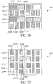
- Figure 19 shows a small portion of a display 190 , including four pixels.
- pixel 192 contains a yellow subpixel 192Y and a cyan subpixel 192C , which are rectangles whose longer axes are aligned parallel to the horizontal.
- red subpixel 192R , green subpixel 192G and blue subpixel 192B are aligned with their longer axes parallel to the vertical.
- Pixel 194 contains the same colored emitters, however the blue subpixel 194B and red subpixel 194R have exchanged positions relative to the positions of 192R and 192B , since they are the low-luminance subpixels, while the high-luminance subpixels have retained their relative positions. As in the previous described embodiments, the sequences of subpixels in alternating and interleaving rows repeat across the height of the display.
- Figure 20 shows a five emitter embodiment consisting of a mixture of rectangular and stripe subpixels.
- a small portion of a display 200 is shown, including four pixels.
- pixel 202 contains four rectangular subpixels, yellow 202Y , red 202R , cyan 202C and blue 202B , plus a green stripe 202G in the center.
- pixel 204 contains four more rectangular emitters of the same color, along with a central green stripe, however the red subpixel 204R and blue subpixel 204B have exchanged positions relative to the positions of 202R and 202B, since they are the low-luminance subpixels, while the high-luminance subpixels have retained their relative positions.
- the sequences of subpixels in alternating and interleaving rows repeat across the height of the display.
- the present invention can be employed in most OLED device configurations that employ four or more different colored OLED subpixel elements, and that include three or more OLED subpixel elements per pixel. These include very unsophisticated structures comprising a separate anode and cathode per OLED to more sophisticated devices, such as passive matrix displays having orthogonal arrays of anodes and cathodes to form pixels, and active-matrix displays where each pixel is controlled independently, for example, with a thin film transistor (TFT).
- TFT thin film transistor
- the present invention can be employed in either a top or bottom emitting OLED device of the types known in the prior art. Such devices employing four or more subpixel elements have been described, e.g., in US Patent Application Publications 2004/0113875 , 2004/0178973 , 2004/0178974 , and 2004/0178743 .
- Similar patterns may alternatively be employed in other OLED display devices containing four or more light emitting subpixel elements in which two light emitting subpixel elements are higher in luminance information than the others.
- commonly assigned USSN 10/812,787 filed March 29, 2004 ) describes an OLED device having red, green, blue and cyan light emitting subpixel elements.
- the green and cyan light emitting subpixel elements provide the preponderance of luminance while the blue and red light emitting subpixel elements once again provide significantly less luminance information.
- the described subpixel arrangements will also be applicable to improving image quality in non-emitting (e.g., transmissive, transflective or reflective) display devices employing liquid crystal, electrowetting or other technologies.
- non-emitting e.g., transmissive, transflective or reflective
- the invention has been described in connection with particular four and five subpixel arrangements, it will be apparent to the artisan that the invention as described and claimed will also be applicable to display devices employing six or even more different types of subpixels.
- specific pixel orientations have been illustrated for various embodiments, further variations within the scope of the appended claims may employ alternative orientations of the subpixels.
- R red subpixel 54B blue subpixel G green subpixel 54W white subpixel B blue subpixel 60 section of a display panel W white subpixel 62 display pixel 10 section of a display panel 62R red subpixel 12 display pixel 62G green subpixel 14 display pixel 62B blue subpixel 16 display pixel 62W white subpixel 18 display pixel 64 display pixel 20 section of a display panel 64R red subpixel 22 display pixel 64G green subpixel 30 section of a display panel 64B blue subpixel 32 display pixel 64W white subpixel 40 section of a display panel 70 section of a display panel 42 display pixel 72 display pixel 42R red subpixel 72R red subpixel 42G green subpixel 72G green subpixel 42B blue subpixel 72B blue subpixel 42W white subpixel 72W white subpixel 44 display pixel 74 display pixel 44R red subpixel 74R red subpixel 44G green subpixel 74G green subpixel 44B blue subpixel 74B blue subpixel 44W white subpixel 74W white subpixel 50 section of
Landscapes
- Engineering & Computer Science (AREA)
- Physics & Mathematics (AREA)
- Computer Hardware Design (AREA)
- General Physics & Mathematics (AREA)
- Theoretical Computer Science (AREA)
- Electroluminescent Light Sources (AREA)
- Devices For Indicating Variable Information By Combining Individual Elements (AREA)
Description
- The present invention relates to color display devices and, more particularly, to arrangements of subpixel elements in such color display devices.
-
US Patent Application Publication 2002/0186214A1, by Siwinski, published December 12, 2002 , shows a method for saving power in an organic light emitting diode (OLED) display having pixels comprised of red, green, blue and white light emitting subpixel elements. The white light emitting subpixel elements are more efficient than the other colored light emitting subpixel elements and are employed to reduce the power requirements of the display. In such a display, the red, green, blue and white light emitting subpixel elements can be illuminated to create any desired color within the gamut of the red, green, and blue light emitting subpixel elements. However, since the white light emitting subpixel elements are more efficient than the red, green, or blue light emitting subpixel element it is desirable to present any neutral color by turning on only the white light emitting subpixel element within a pixel containing the four light emitting subpixel elements. - While power efficiency is always desirable, it is particularly desirable in portable applications because an inefficient display limits the time the device can be used before the power source is recharged. In fact, for certain applications the rate of power consumption may be more important than any other display characteristic with the exception of visibility.
- It has been known for many years that the human eye is most sensitive to greenish yellow light and less sensitive to red and blue light. More specifically, the spatial resolution of the human visual system is driven primarily by the luminance rather than the chrominance of a signal. Since green light provides the preponderance of luminance information in typical viewing environments, the spatial resolution of the visual system during normal daylight viewing conditions is highest for green light, lower for red light, and even lower for blue light when viewing images generated by a typical color balanced image capture and display system. This fact has been used in a variety of ways to optimize the frequency response of imaging systems.
-
US Patent Application Publication 2002/0024618 A1, by Imai, published February 28, 2002 , describes a pixel having a square array of red, green, blue and white light emitting subpixel elements. This pattern may be commonly referred to as a quad pattern. A portion of adisplay device 10 showing an array of foursuch pixels 12 through 18 are shown inFig. 1 . As shown in this figure colors green G and white W having relatively large luminance components are positioned diagonally opposite. At the same time colors red R and blue B produce much less luminance energy than the green and white light emitting subpixel elements. However, because the exact pattern is repeated pixel to pixel, light is often emitted by one or two subpixel elements that are positioned close to one another and, therefore, banding artifacts (i.e., the visibility of dark lines within a row or column of the pixel structure) can be quite visible in this pattern. - It is known in the art to provide pixel patterns with red R, green G, and blue B stripes. A portion of such a
display device 20 is shown inFig. 2 . As shown in this figure, apixel 22 contains red R, green G, and blue B light emitting subpixel elements. Neighboring pixels are positioned within a grid around this pixel such that they are aligned in rows and columns. As with the quad pattern this pixel pattern can exhibit banding artifacts in regions of flat pure primary colors. - It is also known in the art that when relatively large pixels are displayed on a small display or when graphics image regions are likely to be shown that demand a uniform appearance, rows of light emitting subpixel elements may be offset horizontally to reduce the visibility of banding in a
display device 30 as shown inFig. 3 . Commonly referred to as a delta pattern this pattern includes asimilar pixel 32, having red R, green G, and blue B light emitting elements. However, unlike the stripe pattern, this pattern reduces the visibility of banding and improves the uniform appearance in areas of constant color by shifting the alignment of the red, green, and blue subpixel elements in alternating rows. Unfortunately, this pattern creates a visible jagged pattern in vertical lines containing primarily green light emitting subpixel elements as the human eye is very sensitive to offsets in light emitting subpixel elements that are high in luminance. -
EP 1 388 818 A2 discloses an apparatus having an array of subpixels of at least four different colors including two relatively higher luminous color subpixels and two relatively lower luminous color subpixels. A repeating pattern is set forth. -
JP S60-263 122 A - In European Patent Specification
EP 0 330 361 B1, issued April 21, 1993 , Stewart et. al. describe a display device for producing straight vertical and horizontal, and upwardly and downwardly sloping alpha-numeric lines. The pixels of the device were composed of cells ranked in order of brightness: brightest (W), bright (G), medium (R) and darkest (B). In that description the brightest and bright cells were required to be aligned substantially parallel to one axis. -
US 2004/0095521 A1 may be construed to disclose a liquid crystal display, which includes a liquid crystal panel assembly including a plurality of red, green, blue and white pixel areas, and a backlight unit placed at a side of the liquid crystal panel assembly. The light emitted from the backlight unit has a color coordinate (x, y) where x ranges from about 0.31 to about 0.34, and y ranges from about 0.32 to about 0.35. - Additionally, it was required that the bright and darkest cells were diagonally aligned. However, because the exact pattern is repeated pixel to pixel, light is often emitted by one or two subpixel elements that are positioned close to one another and, therefore, banding artifacts (i.e., the visibility of dark lines within a row or column of the pixel structure) can be quite visible in this pattern.
- Additionally, if it is necessary to have cells with unequal area, it is difficult to resize these elements to maintain a symmetric pattern with straight horizontal and vertical gaps between the cells to allow electrical lines to pass through. It is also known to provide an OLED display having pixels with differently sized red, green and blue light emitting subpixel elements, wherein the relative sizes of the subpixel elements in a pixel are selected to extend the service life of the display. See, e.g.,
US 6,366,025 B1, issued April 2, 2002 to Yamada . - There is a need, therefore, for an improved pixel pattern for color display devices that improves the uniformity of a pattern and yet avoids the visibility of jagged vertical or horizontal lines. Ideally, this pixel pattern will provide the enhanced power savings that is available, e.g., from a pattern containing red, green, blue and white subpixels and allow the relative sizes of the light emitting subpixel elements to be readily adjusted.
- According to the disclosure, there is provided a color display device according to
independent claim 1. Developments are set forth in the dependent claims. - Preferably, a color display device is provided, comprising: an array of subpixels of at least four different colors, including at least two relatively higher luminous color subpixels and at least two relatively lower luminous color subpixels, wherein the relatively higher luminous color subpixels are selected from white, green, yellow or cyan subpixels, and the relatively lower luminous color subpixels are blue and red subpixels, the subpixels are arranged into groups forming at least two distinct types of pixels, each pixel type including the two relatively higher luminous color subpixels and at least one of the two relatively lower luminous color subpixels, and the pixel types are arranged in a pattern such that the relative locations of the two relatively higher luminous color subpixels in each pixel is repeated in the adjacent pixels, and the relative location of at least one of the two relatively lower luminance color subpixels is not repeated in at least one adjacent pixel, wherein the at least two relatively higher luminous color subpixels and the at least two relatively lower luminous color subpixels are four different colored subpixels.
- Various embodiments of the invention enable color display devices with improved image display quality, with both the appearance of jagged lines and the appearance of banding reduced simultaneously.
-
-
Fig. 1 is a schematic diagram showing an arrangement of light emitting subpixel elements forming four pixels in a quad arrangement (prior art). -
Fig. 2 is a schematic diagram showing an arrangement of light emitting subpixel elements forming four pixels in a stripe arrangement (prior art). -
Fig. 3 is a schematic diagram showing an arrangement of light emitting subpixel elements forming four pixels in a delta arrangement (prior art); -
Fig. 4 is a schematic diagram showing an arrangement of light emitting subpixel elements according to one embodiment of the present invention. -
Fig. 5 is a schematic diagram showing an arrangement of light emitting subpixel elements according to another embodiment of the present invention. -
Fig. 6 is a schematic diagram showing an arrangement of light emitting subpixel elements according to another embodiment of the present invention. -
Fig. 7 is a schematic diagram showing an arrangement of light emitting subpixel elements according to another embodiment of the present invention. -
Fig. 8 is a schematic diagram showing an arrangement of light emitting subpixel elements according to another embodiment of the present invention. -
Fig. 9 is a schematic diagram showing an arrangement of light emitting subpixel elements according to one embodiment of the present invention. -
Fig. 10 is a schematic diagram showing an arrangement of light emitting subpixel elements according to another embodiment of the present invention. -
Fig. 11 is a schematic diagram showing an arrangement of light emitting subpixel elements according to another embodiment of the present invention. -
Fig. 12 is a schematic diagram showing an arrangement of light emitting subpixel elements according to another embodiment of the present invention. -
Fig. 13 is a schematic diagram showing an arrangement of light emitting subpixel elements according to another embodiment of the present invention. -
Fig. 14 is a schematic diagram showing an arrangement of light emitting subpixel elements according to one embodiment of the present invention. -
Fig. 15 is a schematic diagram showing an arrangement of light emitting subpixel elements according to another embodiment of the present invention. -
Fig. 16 is a schematic diagram showing an arrangement of light emitting subpixel elements according to another embodiment of the present invention. -
Fig. 17 is a schematic diagram showing an arrangement of light emitting subpixel elements according to another embodiment of the present invention. -
Fig. 18 is a schematic diagram showing an arrangement of light emitting subpixel elements according to another embodiment of the present invention. -
Fig. 19 is a schematic diagram showing an arrangement of light emitting subpixel elements according to another embodiment of the present invention. -
Fig. 20 is a schematic diagram showing an arrangement of light emitting subpixel elements according to another embodiment of the present invention. - In accordance with various embodiments described herein, the invention is directed towards a color display device, comprising: an array of subpixels of at least four different colors, including at least two relatively higher luminous color subpixels and at least two relatively lower luminous color subpixels, wherein the subpixels are arranged into groups forming at least two distinct types of pixels, each pixel type including the two relatively higher luminous color subpixels and at least one of the two relatively lower luminous color subpixels, and wherein the pixel types are arranged in a pattern such that the relative locations of the two relatively higher luminous color subpixels in each pixel is repeated in adjacent pixels, and the relative location of at least one of the two relatively lower luminance color subpixels is not repeated in at least one adjacent pixel. In one preferred embodiment, the relatively higher luminous color subpixels are selected from white, green, yellow or cyan subpixels, and the relatively lower luminous color subpixels are blue and red subpixels.
- Research conducted by the present inventors has shown that subpixel elements that bear a significant portion of a display device luminance may be aligned between adjacent pixels within a pattern in accordance with the invention to avoid the appearance of jagged lines. However, subpixel elements that provide a smaller proportion of the display luminance are less likely to provide visible spatial patterns, and need not be aligned between adjacent pixels. The relative positions of subpixel elements that provide a smaller proportion of the display luminance may thus be distributed evenly, switching positions between adjacent pixels, and such locations may contribute to an improvement of the display image uniformity of the pattern.
- In one embodiment of the invention, each of the two distinct pixel types employed include the two relatively lower luminous color subpixels, and the pixel types are arranged such that the relative locations of the two relatively lower luminance color subpixels are interchanged between adjacent pixels in successive rows and/or columns of pixels. Referring to
Fig. 4 , e.g., a display panel 40 (a small portion of which is shown) according to the present invention includes a repeating array of two distinct types ofpixels - The additional subpixel element W is preferably constructed to have a power efficiency that is higher than the power efficiency of at least one of the red R, green G, and blue B light emitting subpixel elements. According to this embodiment of the present invention, the additional light emitting subpixel element provides a greater peak luminance contribution than the peak luminance of either the red or blue subpixel elements. It is well known that the green subpixel element also provides a greater peak luminance contribution than either the red or blue subpixel elements.
- Within this pattern, the white W and green G light emitting subpixel elements are aligned such that the position of each of these subpixel elements is the same for each pixel within the
display device 40. For example, comparing the position of the white W and green G light emitting subpixel element withinpixels subpixel element 42W and 44W is the third light emitting subpixel element within each pixel. Since, these subpixel elements present the majority of the luminance information, positioning the white W and the green G light emitting subpixel elements in horizontal rows and vertical columns, the visibility of jagged lines are avoided within the pattern. - Looking at
pixels subpixel element 42R in onepixel 42 is the first light emitting subpixel element but in the second row the red light emittingsubpixel element 44R is the fourth light emitting subpixel element. Additionally, the blue light emitting subpixel element in thefirst pixel 42B is the fourth light emitting subpixel element but in the succeeding row, the blue light emitting subpixel element 44B is the first light emitting subpixel element. Thus, alternating rows of pixels in the display comprise a first pixel type wherein the subpixels are positioned in a sequence of red, green, white and blue rectangles, whose long axes are oriented vertically, and whose long axes are parallel to each other, said sequence of subpixels in said alternating rows of pixels repeating across the width of the display; and interleaving rows of pixels between the alternating rows in the display comprise a second pixel type wherein the subpixels are positioned in a sequence of blue, green, white and red rectangles, whose long axes are oriented vertically, and whose long axes are parallel to each other, the sequence of subpixels in the interleaving rows of pixels repeating across the width of the display. The sequences of subpixels in alternating and interleaving rows repeat across the height of the display. While the rectangular subpixels are illustrated as being of equal width and length, they may independently be selected to be of different width or length. By separating the red and blue light emitting subpixel elements within the repeating array of light emitting subpixel elements, the uniformity of the pattern is improved and the visibility of banding artifacts are significantly reduced. The fact that this arrangement of light emitting subpixel elements allows both the appearance of jagged lines and the appearance of banding to be reduced simultaneously provides an improvement in overall image quality that has been demonstrated by the present inventors to be greater than it is in patterns where the visibility of only one of these artifacts are reduced at the expense of increasing the visibility of the other. - Referring to
Fig. 5 , a display panel 50 (a small portion of which is shown) includes an alternative arrangement of light emitting subpixel elements within a repeating array of two distinct types ofpixels Fig. 4 . However, the white W and green G columns of pixels are separated to provide a pattern that is more uniform in appearance. As in the previous figure, columns and rows of the luminance bearing light emitting subpixel elements (i.e., white and green) are aligned vertically. That is, 52W and 54W, as well as 52G and 54G are aligned in vertical columns. However, in succeeding rows, the position of the blue B and red R light emitting subpixel elements are displaced in succeeding rows. As shown inFig. 5 the red light emittingsubpixel element 52R is located in the same column and above the blue light emittingsubpixel element 54B. Similarly, the blue light emittingsubpixel element 52B is located in the same column and above the red light emittingsubpixel element 54R. As in the previous described embodiment, the sequences of subpixels in alternating and interleaving rows repeat across the height of the display. - An alternative embodiment is shown in
Fig. 6 . This figure shows a small portion of adisplay panel 60, including an alternative arrangement of light emitting subpixel elements within a repeating array. This figure shows two distinct types ofpixels pixels - An alternate embodiment of the present invention is shown in
Fig.7 . A small portion of adisplay panel 70 is shown that includes four pixels. This is a departure from the quad pattern ofFig. 1 and those known previously in the art. The two distinct types ofpixels pixels Fig. 6 , the position of the red (72R and 74R) and blue (72B and 74B) subpixels are interchanged in succeeding rows of pixels. As in the previous described embodiments, the sequences of subpixels in alternating and interleaving rows repeat across the height of the display. The interchange principle of low luminance subpixels of the present invention is used, resulting in a pattern that is better optimized to the situation where characters, pictorial detail and uniform areas must all be displayed. - Another embodiment of the present invention is shown in
Fig. 8 . A small portion of adisplay panel 80 is shown that includes four pixels. In particular, distinct types ofpixels high luminance subpixels - It is known in the art that the human eye is less sensitive to spatial structure for the light emitting subpixel elements that carry little luminance information. It is further known in the art to subsample these subpixel elements (i.e., include fewer and/or larger light emitting subpixel elements that carry little luminance information than light emitting subpixel elements that carry a larger proportion of the luminance information). Subsampling the pattern shown in
Fig. 5 , an alternative embodiment of the invention is shown inFig. 9 . This figure shows a small portion of adisplay panel 90, including four pixels. Experiments conducted by the present inventors have demonstrated that when this pattern of light emitting subpixel elements replaces the patterns of light emitting subpixel elements such as the ones shown inFig. 4 ,Fig. 5 or Fig. 6 , while applying an equal number of light emitting subpixel elements per area, a sharper and more uniform image appearance results. Alternatively, fewer light emitting subpixel elements per area may be employed, allowing a larger proportion of each pixel to emit light. This is beneficial to the lifetime of emissive displays. - As with the earlier patterns, the white W and green G light emitting subpixel elements are located at the same location within each pixel. Looking at
Fig. 9 , the white (92W and 94W) and green (92G and 94G) light emitting subpixel elements are located at the same position within each pixel. However, due to the fact that the red R and blue B light emitting subpixel elements are subsampled, each pixel contains only one of these two subpixel elements. The red 92R light emitting subpixel element is located in every other pixel. The blue 94B light emitting subpixel element is also located in every other pixel and the blue 94B light emitting subpixel element is located at the same location inpixel 94 as the red 92R light emitting subpixel element is located inpixel 92. The fact that these two pixels are interchanged in successive rows and columns of pixels, reduces the visibility of banding and significantly improves the uniformity of the pattern. As in the previous described embodiments, the sequences of subpixels in alternating and interleaving rows repeat across the height of the display. - To optimize a display device for various applications, differently sized light emitting subpixel elements may be used. Studies conducted by the present inventors have shown that saturated colors occur less frequently than unsaturated colors in both natural and computer generated images and graphics. Hence the efficiency of a display can be improved by using the additional subpixel element in the place of the gamut defining subpixel elements. Moreover, the use of the additional subpixel element can be so high in typical applications that in order to reduce the current density in the additional subpixel element, it is useful to increase the size of the additional subpixel element. Using the example of OLED displays, typical OLED materials presently in use have a relatively higher efficiency for the additional subpixel element and the green subpixel element, and a relatively lower efficiency for the red and blue subpixel elements. Therefore, an optimized display according to the present invention may have relatively larger red, blue and additional subpixel elements, and relatively smaller green subpixel elements. For example, in applications for which the use of black-and-white or low saturation colors dominates, the additional white OLED subpixel elements will be used more heavily than any of the gamut defining subpixel elements and may therefore be increased in size to reduce the current density and hence aging of the additional subpixel element. Text, graphic, and pictorial based applications are typically of these types.
- One embodiment of the present invention including subpixels of varying size is shown in
Fig. 10 . A small portion of adisplay panel 100 is shown, including four pixels. In particular, distinct types ofpixels red subpixel 102R, but not a blue subpixel, whereas 104 contains ablue subpixel 104B, but not a red subpixel. Note that the size of the red and blue subpixels is the same, and both are larger than the G or W subpixels. The position of the red and blue subpixels alternates as shown previously inFig. 9 . This results in a pattern that is classified as neither stripe nor quad, but does adhere to the design principles of high luminance subpixel alignment and low luminance subpixel interchange of the present invention. As in the previous described embodiments, the sequences of subpixels in alternating and interleaving rows repeat across the height of the display. It should be noted that since there are fewer red and blue light emitting subpixels than white and green light emitting subpixels within the pattern depicted inFig. 10 , the use of this pattern may require these elements to have twice the area as they would have in the patterns shown inFig. 4 ,Fig. 5 or Fig. 6 in order to achieve proper color balance or to balance the lifetimes of the subpixels. - The orientation of the pattern shown in
Fig. 10 can be rotated. One such orientation of this pattern is shown inFig. 11. Fig. 11 shows a small portion of adisplay panel 110, including four pixels. As was shown inFig. 10 , each pixel consists of white W, green G, and either one red R or one blue B light emitting subpixel element, but not both. For example, apixel 112 consists of a red 112R, green 112G, and white 112W light emitting subpixel element. A neighboringpixel 114 consists of a blue 114B, green 114G and white 114W light emitting subpixel elements. This pattern provides white (e.g., 112W and 114W) and green (e.g., 112G and 114G) light emitting subpixel elements that are positioned at the same locations within each pixel while the position of red 112R and blue 114B light emitting subpixel elements are the same in the two pixels. As in the previous described embodiments, the sequences of subpixels in alternating and interleaving rows repeat across the height of the display. - Another embodiment of the invention demonstrating varying subpixel sizes is shown in
Fig. 12 . A small portion of adisplay panel 120 is shown, including four pixels. In particular, distinct types ofpixels red subpixel 122R, but not a blue subpixel, whereas 124 contains ablue subpixel 124B, but not a red subpixel. Note that the size of the red, green and blue subpixels are the same, and all three are smaller than the W subpixel. The position of the red and blue subpixels alternates as demonstrated previously. As in the previous described embodiments, the sequences of subpixels in alternating and interleaving rows repeat across the height of the display. - The previous embodiments of the invention have demonstrated instances in which the combined subpixel aperture ratio is at or near the maximum, that is, nearly all available space within the pixel is emitting. The subpixel aperture ratio is defined as the ratio of the active or emitting subpixel area to the total pixel area. For various reasons, such as the need to include supporting circuitry, the full area of the pixel will not be actively emitting radiation. An embodiment of the invention demonstrating a much smaller than maximum subpixel aperture ratio is shown in
Fig. 13 . This embodiment is completely analogous in its arrangement to that shown inFig. 9 , the difference being the much smaller (roughly one half as large) subpixel aperture ratio. The white (132W and 134W) and green (132G and 134G) light emitting subpixel elements are located at the same position within each pixel. The red 132R light emitting subpixel element is located in every other pixel. The blue 134B light emitting subpixel element is also located in every other pixel and the blue 134B light emitting subpixel element is located at the same location inpixel 134 as the red 132R light emitting subpixel element is located inpixel 132. It will be appreciated that the invention can be readily applied to a continuum of other subpixel aperture ratios. As in the previous described embodiments, the sequences of subpixels in alternating and interleaving rows repeat across the height of the display. - The above discussed display embodiments each employ combinations of four different colored subpixels. Alternate embodiments of the invention for five light emitting subpixel elements are now demonstrated.
Figure 14 shows a small portion of adisplay panel 140, including four pixels. In particular,pixel 142 contains, from left to right, a yellow emittingsubpixel 142Y, blue emittingsubpixel 142B, green emittingsubpixel 142G,cyan emitting subpixel 142C, and red emittingsubpixel 142R. Subpixels such as yellow and cyan may be used to enhance the efficiency, lifetime and/or color gamut of a display device.Pixel 144 contains the same selection of colored emitters. However, in 144 the arrangement is, again from left to right, yellow (144Y), red (144R), green (144G), cyan (144C) and blue (144B). As before, the subpixels carrying the majority of the luminance information, i.e. green, yellow and cyan, retain their relative position and alignment within the pixel, while the other subpixels alternate positions. As in the previous described embodiments, the sequences of subpixels in alternating and interleaving rows repeat across the height of the display. - An alternate embodiment of a five emitter striped display with subsampling of the low-luminance red and blue subpixel elements is shown in
Fig. 15 . A small portion of adisplay 150 is shown, including four pixels. In particular,pixel 152 contains ayellow subpixel 152Y,blue subpixel 152B,green subpixel 152G, and cyan subpixel 152C, but does not contain a red subpixel.Pixel 154 contains ayellow subpixel 154Y,red subpixel 154R,green subpixel 154G, and cyan subpixel 154C, but does not contain a blue subpixel. The red and blue subpixels are seen to alternate, in analogy withFig. 9 for the four emitter display. As in the previous described embodiments, the sequences of subpixels in alternating and interleaving rows repeat across the height of the display. - An alternate embodiment for a five emitter display is shown in
Fig. 16 . A small portion of adisplay panel 160 is shown, including four pixels. In particular,pixel 162 contains ayellow subpixel 162Y,green subpixel 162G, cyan subpixel 162C andred subpixel 162R.Pixel 164 contains ayellow subpixel 164Y,green subpixel 164G and cyan subpixel 164C, but contains ablue subpixel 164B rather than a red subpixel. As before, the high-luminance subpixels retain their positions while the low-luminance red and blue subpixels appear in every other group of subpixels. As in the previous described embodiments, the sequences of subpixels in alternating and interleaving rows repeat across the height of the display. -
Figure 17 shows an alternate embodiment to that shown inFig. 16 . A small portion of adisplay panel 170 is shown, including four pixels. In particular,pixel 172 contains ayellow subpixel 172Y,red subpixel 172R, cyan subpixel 172C andgreen subpixel 172G.Pixel 174 contains ayellow subpixel 174Y,blue subpixel 174B, cyan subpixel 174C, andgreen subpixel 174G. As before, the high-luminance subpixels retain their positions while the low-luminance red and blue subpixels appear in every other group of subpixels. As in the previous described embodiments, the sequences of subpixels in alternating and interleaving rows repeat across the height of the display. -
Figure 18 shows an alternate embodiment for a five emitter display. A small portion of adisplay panel 180 is shown, including four pixels. In particular,pixel 182 contains ayellow subpixel 182Y,green subpixel 182G, cyan subpixel 182C andred subpixel 182R.Pixel 184 contains ayellow subpixel 184Y,blue subpixel 184B, cyan subpixel 184C, andgreen subpixel 184G. In this case, the yellow and cyan are treated as the high-luminance subpixels, while the red, green and blue are treated as the low-luminance subpixels. The red and blue are subsampled, and all three of the red, green and blue alternate positions between groups. As in the previous described embodiments, the sequences of subpixels in alternating and interleaving rows repeat across the height of the display. - Other five emitter arrangements and subpixel geometries are possible within the scope of the invention.
Figure 19 shows a small portion of adisplay 190, including four pixels. In particular,pixel 192 contains ayellow subpixel 192Y and a cyan subpixel 192C, which are rectangles whose longer axes are aligned parallel to the horizontal. Within the same grouping,red subpixel 192R,green subpixel 192G andblue subpixel 192B are aligned with their longer axes parallel to the vertical.Pixel 194 contains the same colored emitters, however theblue subpixel 194B andred subpixel 194R have exchanged positions relative to the positions of 192R and 192B, since they are the low-luminance subpixels, while the high-luminance subpixels have retained their relative positions. As in the previous described embodiments, the sequences of subpixels in alternating and interleaving rows repeat across the height of the display. -
Figure 20 shows a five emitter embodiment consisting of a mixture of rectangular and stripe subpixels. A small portion of adisplay 200 is shown, including four pixels. In particular,pixel 202 contains four rectangular subpixels, yellow 202Y, red 202R,cyan 202C and blue 202B, plus agreen stripe 202G in the center. Below this group,pixel 204 contains four more rectangular emitters of the same color, along with a central green stripe, however thered subpixel 204R andblue subpixel 204B have exchanged positions relative to the positions of 202R and 202B, since they are the low-luminance subpixels, while the high-luminance subpixels have retained their relative positions. As in the previous described embodiments, the sequences of subpixels in alternating and interleaving rows repeat across the height of the display. - The present invention can be employed in most OLED device configurations that employ four or more different colored OLED subpixel elements, and that include three or more OLED subpixel elements per pixel. These include very unsophisticated structures comprising a separate anode and cathode per OLED to more sophisticated devices, such as passive matrix displays having orthogonal arrays of anodes and cathodes to form pixels, and active-matrix displays where each pixel is controlled independently, for example, with a thin film transistor (TFT). The present invention can be employed in either a top or bottom emitting OLED device of the types known in the prior art. Such devices employing four or more subpixel elements have been described, e.g., in
US Patent Application Publications 2004/0113875 ,2004/0178973 ,2004/0178974 , and2004/0178743 . - Similar patterns may alternatively be employed in other OLED display devices containing four or more light emitting subpixel elements in which two light emitting subpixel elements are higher in luminance information than the others. For example, commonly assigned
USSN 10/812,787 (filed March 29, 2004 - While the invention is particularly applicable, and has been particularly described in connection with the arrangement of subpixel elements employed in light emitting displays such as OLED displays, Plasma or Field Emission displays, the described subpixel arrangements will also be applicable to improving image quality in non-emitting (e.g., transmissive, transflective or reflective) display devices employing liquid crystal, electrowetting or other technologies. Further, while the invention has been described in connection with particular four and five subpixel arrangements, it will be apparent to the artisan that the invention as described and claimed will also be applicable to display devices employing six or even more different types of subpixels. Further, it will be apparent to the artisan that while specific pixel orientations have been illustrated for various embodiments, further variations within the scope of the appended claims may employ alternative orientations of the subpixels.
PARTS LIST R red subpixel 54B blue subpixel G green subpixel 54W white subpixel B blue subpixel 60 section of a display panel W white subpixel 62 display pixel 10 section of a display panel 62R red subpixel 12 display pixel 62G green subpixel 14 display pixel 62B blue subpixel 16 display pixel 62W white subpixel 18 display pixel 64 display pixel 20 section of a display panel 64R red subpixel 22 display pixel 64G green subpixel 30 section of a display panel 64B blue subpixel 32 display pixel 64W white subpixel 40 section of a display panel 70 section of a display panel 42 display pixel 72 display pixel 42R red subpixel 72R red subpixel 42G green subpixel 72G green subpixel 42B blue subpixel 72B blue subpixel 42W white subpixel 72W white subpixel 44 display pixel 74 display pixel 44R red subpixel 74R red subpixel 44G green subpixel 74G green subpixel 44B blue subpixel 74B blue subpixel 44W white subpixel 74W white subpixel 50 section of a display panel 80 section of a display panel 52 display pixel 82 display pixel 52R red subpixel 82R red subpixel 52G green subpixel 82G green subpixel 52B blue subpixel 82B blue subpixel 52W white subpixel 82W white subpixel 54 display pixel 84 display pixel 54R red subpixel 84R red subpixel 54G green subpixel 84G green subpixel 84B blue subpixel 124 display pixel 84W white subpixel 124G green subpixel 90 section of a display panel 124B blue subpixel 92 display pixel 124W white subpixel 92R red subpixel 130 section of a display panel 92G green subpixel 132 display pixel 92W white subpixel 132R red subpixel 94 display pixel 132G green subpixel 94G green subpixel 132W white subpixel 94B blue subpixel 134 display pixel 94W white subpixel 134G green subpixel 100 section of a display panel 134B blue subpixel 102 display pixel 134W white subpixel 102R red subpixel 40 section of a display panel 102G green subpixel 142 display pixel 102W white subpixel 142R red subpixel 104 display pixel 142G green subpixel 104G green subpixel 142B blue subpixel 104B blue subpixel 142Y yellow subpixel 104W white subpixel 142C cyan subpixel 110 section of a display panel 144 display pixel 112 display pixel 144G green subpixel 112R red subpixel 144B blue subpixel 112G green subpixel 144R red subpixel 112W white subpixel 144Y yellow subpixel 114 display pixel 144C cyan subpixel 114G green subpixel 150 section of a display panel 114B blue subpixel 152 display pixel 114W white subpixel 152G green subpixel 120 section of a display panel 152B blue subpixel 122 display pixel 152Y yellow subpixel 122R red subpixel 152C cyan subpixel 122G green subpixel 154 display pixel 122W white subpixel 154G green subpixel 154R red subpixel 184Y yellow subpixel 154Y yellow subpixel 184C cyan subpixel 154C cyan subpixel 190 section of a display panel 160 section of a display panel 192 display pixel 162 display pixel 192R red subpixel 162R red subpixel 192G green subpixel 162G green subpixel 192B blue subpixel 162Y yellow subpixel 192Y yellow subpixel 162C cyan subpixel 192C cyan subpixel 164 display pixel 194 display pixel 164G green subpixel 194G green subpixel 164B blue subpixel 194B blue subpixel 164Y yellow subpixel 194R red subpixel 164C cyan subpixel 194Y yellow subpixel 170 section of a display panel 194C cyan subpixel 172 display pixel 172R red subpixel 172G green subpixel 172Y yellow subpixel 172C cyan subpixel 174 display pixel 174G green subpixel 174B blue subpixel 174Y yellow subpixel 174C cyan subpixel 180 section of a display panel 182 display pixel 182R red subpixel 182G green subpixel 182Y yellow subpixel 182C cyan subpixel 184 display pixel 184G green subpixel 184B blue subpixel
Claims (3)
- A color display device, comprising:an array of subpixels (40, 50, 60, 70, 80, 90, 100, 110, 120, 130) of at least four different colors, including at least two relatively higher luminous color subpixels (42G, 42W, 52G, 52W, 62G, 62W, 72G, 72W, 82G, 82W, 92G, 92W, 102G, 102W, 112G, 112W, 122G, 122W, 132G, 132W) and at least two relatively lower luminous color subpixels (42R, 42B, 52R, 52B, 62R, 62B, 72R, 72B, 82R, 82B, 92R, 92B, 102R, 102B, 112R, 112B, 122R, 122B, 132R, 132B), whereinthe relatively higher luminous color subpixels are selected from white, green, yellow or cyan subpixels, and the relatively lower luminous color subpixels are blue and red subpixels,the subpixels are arranged into groups (42, 44, 52, 54, 62, 64, 72, 74, 82, 84, 92, 94, 102, 104, 112, 114, 122, 124, 132, 134) forming at least two distinct types of pixels, each pixel type including the two relatively higher luminous color subpixels and at least one of the two relatively lower luminous color subpixels, andthe pixel types being arranged in a pattern such that the relative locations of the two relatively higher luminous color subpixels in each pixel is repeated in the adjacent pixels, and the relative location of at least one of the two relatively lower luminance color subpixels is not repeated in at least one adjacent pixel,characterized in thatthe at least two relatively higher luminous color subpixels and the at least two relatively lower luminous color subpixels are four different colored subpixels.
- The color display device according to claim 1, wherein:alternating rows of pixels in the display comprise a first pixel type wherein the subpixels are positioned in a sequence of red (42R), green (42G), white (42W) and blue (42B) rectangles, whose long axes are oriented vertically, and whose long axes are parallel to each other, said sequence of subpixels in said alternating rows of pixels repeating across the width of the display; andinterleaving rows of pixels between the alternating rows in the display comprise a second pixel type wherein the subpixels are positioned in a sequence of blue (42B), green (42G), white (42W) and red (42R) rectangles, whose long axes are oriented vertically, and whose long axes are parallel to each other, said sequence of subpixels in said interleaving rows of pixels repeating across the width of the display; andsaid sequences of subpixels in alternating and interleaving rows repeating across the height of the display.
- The color display device according to claim 1, wherein each of the two distinct pixel types exclude a different one of the two relatively lower luminous color subpixels, and where the pixel types are arranged such that the excluded relatively lower luminance color subpixels (92R, 94B, 102R, 104B, 112R, 114B, 122R, 124B, 132R, 134B) are interchanged between adjacent pixels in successive rows or columns of pixels.
Applications Claiming Priority (2)
| Application Number | Priority Date | Filing Date | Title |
|---|---|---|---|
| US10/859,314 US7515122B2 (en) | 2004-06-02 | 2004-06-02 | Color display device with enhanced pixel pattern |
| PCT/US2005/019119 WO2005122122A1 (en) | 2004-06-02 | 2005-06-01 | Color display device with enhanced pixel pattern |
Publications (2)
| Publication Number | Publication Date |
|---|---|
| EP1756796A1 EP1756796A1 (en) | 2007-02-28 |
| EP1756796B1 true EP1756796B1 (en) | 2019-01-23 |
Family
ID=34971074
Family Applications (1)
| Application Number | Title | Priority Date | Filing Date |
|---|---|---|---|
| EP05754388.6A Active EP1756796B1 (en) | 2004-06-02 | 2005-06-01 | Color display device with enhanced pixel pattern |
Country Status (4)
| Country | Link |
|---|---|
| US (1) | US7515122B2 (en) |
| EP (1) | EP1756796B1 (en) |
| JP (1) | JP4870664B2 (en) |
| WO (1) | WO2005122122A1 (en) |
Families Citing this family (107)
| Publication number | Priority date | Publication date | Assignee | Title |
|---|---|---|---|---|
| JP4003714B2 (en) * | 2003-08-11 | 2007-11-07 | セイコーエプソン株式会社 | Electro-optical device and electronic apparatus |
| EP1704555A4 (en) * | 2003-12-15 | 2009-03-11 | Genoa Color Technologies Ltd | Multi-primary liquid crystal display |
| US7495722B2 (en) * | 2003-12-15 | 2009-02-24 | Genoa Color Technologies Ltd. | Multi-color liquid crystal display |
| KR101303372B1 (en) * | 2004-06-04 | 2013-09-03 | 코닌클리즈케 필립스 일렉트로닉스 엔.브이. | Electroluminescent structure and led with an el structure |
| KR100866236B1 (en) * | 2004-08-19 | 2008-10-30 | 샤프 가부시키가이샤 | Multiple primary color display |
| US7973811B2 (en) * | 2005-01-25 | 2011-07-05 | Panasonic Corporation | Display device |
| JP4646977B2 (en) * | 2005-04-05 | 2011-03-09 | シャープ株式会社 | Color filter substrate and display device |
| JP4211773B2 (en) * | 2005-05-19 | 2009-01-21 | エプソンイメージングデバイス株式会社 | Electro-optical device and electronic apparatus |
| JP4823571B2 (en) * | 2005-05-30 | 2011-11-24 | 株式会社 日立ディスプレイズ | 3D display device |
| US7898623B2 (en) | 2005-07-04 | 2011-03-01 | Semiconductor Energy Laboratory Co., Ltd. | Display device, electronic device and method of driving display device |
| CN101233552B (en) * | 2005-07-29 | 2010-05-19 | 夏普株式会社 | Display |
| WO2007034770A1 (en) * | 2005-09-21 | 2007-03-29 | Sharp Kabushiki Kaisha | Display device and color filter substrate |
| EP1770676B1 (en) | 2005-09-30 | 2017-05-03 | Semiconductor Energy Laboratory Co., Ltd. | Display device and electronic device |
| WO2007060672A2 (en) | 2005-11-28 | 2007-05-31 | Genoa Color Technologies Ltd. | Sub-pixel rendering of a multiprimary image |
| KR20070063169A (en) * | 2005-12-14 | 2007-06-19 | 삼성전자주식회사 | Liquid crystal display |
| US8207924B2 (en) * | 2006-02-02 | 2012-06-26 | Sharp Kabushiki Kaisha | Display device |
| TWI275052B (en) * | 2006-04-07 | 2007-03-01 | Ind Tech Res Inst | OLED pixel structure and method of manufacturing the same |
| US7876341B2 (en) * | 2006-08-28 | 2011-01-25 | Samsung Electronics Co., Ltd. | Subpixel layouts for high brightness displays and systems |
| JP5403860B2 (en) | 2006-10-10 | 2014-01-29 | 株式会社ジャパンディスプレイ | Color liquid crystal display device |
| CN101206273A (en) * | 2006-12-22 | 2008-06-25 | 群康科技(深圳)有限公司 | Color filters and liquid crystal display panel using the same |
| US8013817B2 (en) | 2006-12-27 | 2011-09-06 | Global Oled Technology Llc | Electronic display having improved uniformity |
| EP2109091B1 (en) * | 2007-01-25 | 2016-09-07 | Sharp Kabushiki Kaisha | Multi-primary-color display device |
| EP2733518B1 (en) * | 2007-02-13 | 2016-07-27 | Samsung Display Co., Ltd. | Subpixel layouts and subpixel rendering methods for directional displays and systems |
| US20080203899A1 (en) * | 2007-02-28 | 2008-08-28 | Miller Michael E | Electro-luminescent display with improved efficiency |
| KR100892225B1 (en) * | 2007-04-16 | 2009-04-09 | 삼성전자주식회사 | Color display apparatus |
| CN101393924B (en) * | 2007-09-21 | 2015-08-12 | 北京京东方光电科技有限公司 | Electroluminescence display panel |
| US8154527B2 (en) | 2008-01-04 | 2012-04-10 | Tactus Technology | User interface system |
| US8456438B2 (en) | 2008-01-04 | 2013-06-04 | Tactus Technology, Inc. | User interface system |
| US9128525B2 (en) | 2008-01-04 | 2015-09-08 | Tactus Technology, Inc. | Dynamic tactile interface |
| US9430074B2 (en) | 2008-01-04 | 2016-08-30 | Tactus Technology, Inc. | Dynamic tactile interface |
| US9760172B2 (en) | 2008-01-04 | 2017-09-12 | Tactus Technology, Inc. | Dynamic tactile interface |
| US9298261B2 (en) | 2008-01-04 | 2016-03-29 | Tactus Technology, Inc. | Method for actuating a tactile interface layer |
| US9612659B2 (en) | 2008-01-04 | 2017-04-04 | Tactus Technology, Inc. | User interface system |
| US9013417B2 (en) | 2008-01-04 | 2015-04-21 | Tactus Technology, Inc. | User interface system |
| US9552065B2 (en) | 2008-01-04 | 2017-01-24 | Tactus Technology, Inc. | Dynamic tactile interface |
| US9423875B2 (en) | 2008-01-04 | 2016-08-23 | Tactus Technology, Inc. | Dynamic tactile interface with exhibiting optical dispersion characteristics |
| US20140152611A1 (en) * | 2012-06-01 | 2014-06-05 | Tactus Technology, Inc. | User interface |
| US9588683B2 (en) | 2008-01-04 | 2017-03-07 | Tactus Technology, Inc. | Dynamic tactile interface |
| US8243038B2 (en) | 2009-07-03 | 2012-08-14 | Tactus Technologies | Method for adjusting the user interface of a device |
| US9720501B2 (en) | 2008-01-04 | 2017-08-01 | Tactus Technology, Inc. | Dynamic tactile interface |
| US9274612B2 (en) | 2008-01-04 | 2016-03-01 | Tactus Technology, Inc. | User interface system |
| US8947383B2 (en) | 2008-01-04 | 2015-02-03 | Tactus Technology, Inc. | User interface system and method |
| US8587541B2 (en) | 2010-04-19 | 2013-11-19 | Tactus Technology, Inc. | Method for actuating a tactile interface layer |
| US9063627B2 (en) | 2008-01-04 | 2015-06-23 | Tactus Technology, Inc. | User interface and methods |
| US9557915B2 (en) | 2008-01-04 | 2017-01-31 | Tactus Technology, Inc. | Dynamic tactile interface |
| JP5078653B2 (en) * | 2008-02-13 | 2012-11-21 | セイコーインスツル株式会社 | Color filter substrate, liquid crystal display device and display device |
| JP4807366B2 (en) * | 2008-03-11 | 2011-11-02 | ソニー株式会社 | Display device |
| JP4623114B2 (en) * | 2008-03-23 | 2011-02-02 | ソニー株式会社 | EL display panel and electronic device |
| US9588684B2 (en) | 2009-01-05 | 2017-03-07 | Tactus Technology, Inc. | Tactile interface for a computing device |
| DE102009038469B4 (en) | 2009-08-21 | 2015-02-12 | Advanced Display Technology Ag | Display element and method for driving a display element |
| KR101042955B1 (en) * | 2009-09-02 | 2011-06-20 | 삼성모바일디스플레이주식회사 | Organic light emitting display apparatus with touch screen |
| EP2517089A4 (en) | 2009-12-21 | 2016-03-09 | Tactus Technology | User interface system |
| US9239623B2 (en) | 2010-01-05 | 2016-01-19 | Tactus Technology, Inc. | Dynamic tactile interface |
| US20110164068A1 (en) * | 2010-01-06 | 2011-07-07 | Qualcomm Mems Technologies, Inc. | Reordering display line updates |
| WO2011112984A1 (en) | 2010-03-11 | 2011-09-15 | Tactus Technology | User interface system |
| KR20110129531A (en) * | 2010-05-26 | 2011-12-02 | 삼성모바일디스플레이주식회사 | Pixel array for organic light emitting display device |
| US8537086B2 (en) * | 2010-06-16 | 2013-09-17 | Semiconductor Energy Laboratory Co., Ltd. | Driving method of liquid crystal display device |
| US9583034B2 (en) * | 2010-10-15 | 2017-02-28 | Lg Display Co., Ltd. | Subpixel arrangement structure for display device |
| KR20140043697A (en) | 2010-10-20 | 2014-04-10 | 택투스 테크놀로지, 아이엔씨. | User interface system and method |
| JP5884385B2 (en) * | 2011-10-06 | 2016-03-15 | セイコーエプソン株式会社 | Image processing apparatus, display apparatus, and image processing method |
| JP2013120321A (en) * | 2011-12-08 | 2013-06-17 | Sony Corp | Display unit and electronic apparatus |
| US9165526B2 (en) * | 2012-02-28 | 2015-10-20 | Shenzhen Yunyinggu Technology Co., Ltd. | Subpixel arrangements of displays and method for rendering the same |
| CN102759819B (en) * | 2012-07-13 | 2014-10-29 | 京东方科技集团股份有限公司 | Color film substrate, array substrate, liquid crystal panel and liquid crystal display device |
| KR101996432B1 (en) * | 2012-09-19 | 2019-07-05 | 삼성디스플레이 주식회사 | Display Device and Driving Method thereof |
| WO2014047656A2 (en) | 2012-09-24 | 2014-03-27 | Tactus Technology, Inc. | Dynamic tactile interface and methods |
| US9405417B2 (en) | 2012-09-24 | 2016-08-02 | Tactus Technology, Inc. | Dynamic tactile interface and methods |
| JP5910529B2 (en) * | 2013-02-15 | 2016-04-27 | ソニー株式会社 | Display device and electronic device |
| JP2014186257A (en) * | 2013-03-25 | 2014-10-02 | Sony Corp | Display device and electronic apparatus |
| JP5849981B2 (en) * | 2013-03-25 | 2016-02-03 | ソニー株式会社 | Display device and electronic device |
| JP2014203004A (en) * | 2013-04-08 | 2014-10-27 | 株式会社ジャパンディスプレイ | Display device and electronic apparatus |
| KR20140126568A (en) * | 2013-04-23 | 2014-10-31 | 삼성디스플레이 주식회사 | Organic light emitting diode display |
| TWI536076B (en) * | 2013-06-11 | 2016-06-01 | 友達光電股份有限公司 | Pixel array and color development compensating method |
| US9557813B2 (en) | 2013-06-28 | 2017-01-31 | Tactus Technology, Inc. | Method for reducing perceived optical distortion |
| TWI522992B (en) * | 2013-10-30 | 2016-02-21 | 友達光電股份有限公司 | Pixel array structure of color display panel |
| CN104752469B (en) * | 2013-12-31 | 2018-08-03 | 昆山国显光电有限公司 | A kind of dot structure and the organic light emitting display using the dot structure |
| CN103913868A (en) * | 2014-04-08 | 2014-07-09 | 深圳市华星光电技术有限公司 | Liquid-crystal display and imaging control method |
| US20150287767A1 (en) * | 2014-04-08 | 2015-10-08 | Apple Inc. | Organic Light-Emitting Diode Display With Varying Anode Pitch |
| JP6480669B2 (en) * | 2014-04-15 | 2019-03-13 | 株式会社ジャパンディスプレイ | Display device, display device driving method, and electronic apparatus |
| JP6324207B2 (en) * | 2014-05-16 | 2018-05-16 | 株式会社ジャパンディスプレイ | Display device |
| TWI525379B (en) * | 2014-06-04 | 2016-03-11 | 聯詠科技股份有限公司 | Display device and driving module thereof |
| JP6393529B2 (en) * | 2014-06-18 | 2018-09-19 | 株式会社ジャパンディスプレイ | Liquid crystal display |
| CN104112763B (en) * | 2014-06-30 | 2017-07-04 | 京东方科技集团股份有限公司 | A kind of pixel arrangement structure, display device and its display methods |
| CN104361850B (en) * | 2014-11-04 | 2018-05-04 | 京东方科技集团股份有限公司 | A kind of dot structure and its driving method, display device |
| JP6386892B2 (en) | 2014-11-28 | 2018-09-05 | 株式会社ジャパンディスプレイ | Display device |
| TWI556048B (en) * | 2014-12-02 | 2016-11-01 | 聯詠科技股份有限公司 | Display device and driving module thereof |
| JP6427403B2 (en) | 2014-12-15 | 2018-11-21 | 株式会社ジャパンディスプレイ | Display device |
| EP3043558B1 (en) * | 2014-12-21 | 2022-11-02 | Production Resource Group, L.L.C. | Large-format display systems having color pixels and white pixels |
| KR102357161B1 (en) * | 2015-01-20 | 2022-01-28 | 삼성디스플레이 주식회사 | Curved liquid crystal display device |
| JP2016139071A (en) * | 2015-01-29 | 2016-08-04 | 株式会社ジャパンディスプレイ | Display device |
| JP2016161920A (en) | 2015-03-05 | 2016-09-05 | 株式会社ジャパンディスプレイ | Display device |
| JP2016200769A (en) * | 2015-04-14 | 2016-12-01 | 株式会社ジャパンディスプレイ | Display device |
| KR102306652B1 (en) * | 2015-04-28 | 2021-09-29 | 삼성디스플레이 주식회사 | Display device and driving method thereof |
| CN104914606A (en) * | 2015-06-16 | 2015-09-16 | 深圳市华星光电技术有限公司 | Touch control panel and driving method thereof |
| TWI587006B (en) * | 2015-06-30 | 2017-06-11 | 友達光電股份有限公司 | Display device and head up display |
| JP2017037179A (en) * | 2015-08-10 | 2017-02-16 | 株式会社ジャパンディスプレイ | Display and driving method thereof |
| JP2018072676A (en) * | 2016-11-01 | 2018-05-10 | 株式会社ジャパンディスプレイ | Display device |
| TWI606275B (en) | 2016-12-29 | 2017-11-21 | 友達光電股份有限公司 | Pixel matrix and display method thereof |
| CN106855672A (en) * | 2017-02-28 | 2017-06-16 | 京东方科技集团股份有限公司 | Array base palte and its manufacture method, display panel and display device |
| CN107359187B (en) * | 2017-08-17 | 2020-07-03 | 武汉华星光电半导体显示技术有限公司 | OLED pixel unit, display panel and electronic equipment |
| CN109427852B (en) * | 2017-08-31 | 2021-09-10 | 昆山国显光电有限公司 | Pixel structure, mask and display device |
| US11181742B2 (en) * | 2018-10-05 | 2021-11-23 | Samsung Electronics Co., Ltd. | Display panel, and 3D display device and 3D head up display (HUD) device using the display panel |
| KR20200039527A (en) * | 2018-10-05 | 2020-04-16 | 삼성전자주식회사 | DISPLAY PANEL, 3D DISPLAY APPARATUS AND 3D Head Up Display(HUD) DEVICE USING THE SAME |
| CN109638035B (en) * | 2018-11-13 | 2021-02-26 | 武汉华星光电半导体显示技术有限公司 | Pixel arrangement structure and organic light emitting diode display device |
| US11139348B2 (en) | 2018-11-27 | 2021-10-05 | Samsung Display Co., Ltd. | Display device |
| CN109343276B (en) * | 2018-11-29 | 2021-04-30 | 厦门天马微电子有限公司 | Display module and display device |
| KR20220019195A (en) * | 2020-08-07 | 2022-02-16 | 삼성디스플레이 주식회사 | Display device |
| CN113093431A (en) * | 2021-04-08 | 2021-07-09 | Oppo广东移动通信有限公司 | Electronic device, display module and display panel thereof |
Citations (4)
| Publication number | Priority date | Publication date | Assignee | Title |
|---|---|---|---|---|
| JPS60263122A (en) * | 1984-06-11 | 1985-12-26 | Seiko Epson Corp | Color display panel |
| EP0330361A2 (en) * | 1988-02-16 | 1989-08-30 | General Electric Company | Color display device |
| EP1388818A2 (en) * | 2002-08-10 | 2004-02-11 | Samsung Electronics Co., Ltd. | Method and apparatus for rendering image signal |
| US20040095521A1 (en) * | 2002-11-20 | 2004-05-20 | Keun-Kyu Song | Four color liquid crystal display and panel therefor |
Family Cites Families (20)
| Publication number | Priority date | Publication date | Assignee | Title |
|---|---|---|---|---|
| JPS59119679A (en) | 1982-12-27 | 1984-07-10 | Toshiba Corp | Electrode for fuel cell |
| US5341153A (en) * | 1988-06-13 | 1994-08-23 | International Business Machines Corporation | Method of and apparatus for displaying a multicolor image |
| JP2584490B2 (en) * | 1988-06-13 | 1997-02-26 | 三菱電機株式会社 | Matrix type liquid crystal display |
| US5339092A (en) * | 1989-11-06 | 1994-08-16 | Honeywell Inc | Beam former for matrix display |
| US5485293A (en) * | 1993-09-29 | 1996-01-16 | Honeywell Inc. | Liquid crystal display including color triads with split pixels |
| US5781257A (en) * | 1995-01-30 | 1998-07-14 | Lockheed Martin Missiles & Space Co | Flat panel display |
| JPH1010998A (en) * | 1996-06-26 | 1998-01-16 | Canon Inc | Colour display device |
| US6188385B1 (en) * | 1998-10-07 | 2001-02-13 | Microsoft Corporation | Method and apparatus for displaying images such as text |
| US6366025B1 (en) * | 1999-02-26 | 2002-04-02 | Sanyo Electric Co., Ltd. | Electroluminescence display apparatus |
| US6384839B1 (en) * | 1999-09-21 | 2002-05-07 | Agfa Monotype Corporation | Method and apparatus for rendering sub-pixel anti-aliased graphics on stripe topology color displays |
| US7113231B2 (en) * | 2000-02-14 | 2006-09-26 | 3M Innovative Properties Company | Dot-sequential color display system |
| JP2002072980A (en) * | 2000-08-31 | 2002-03-12 | Nec Corp | Color video display method and device |
| US7184066B2 (en) * | 2001-05-09 | 2007-02-27 | Clairvoyante, Inc | Methods and systems for sub-pixel rendering with adaptive filtering |
| US7012588B2 (en) * | 2001-06-05 | 2006-03-14 | Eastman Kodak Company | Method for saving power in an organic electroluminescent display using white light emitting elements |
| IL159246A0 (en) | 2001-06-11 | 2004-06-01 | Genoa Technologies Ltd | Device, system and method for color display |
| CN1324363C (en) * | 2002-05-04 | 2007-07-04 | 三星电子株式会社 | LCD device and filtering color picec array board |
| US20040080479A1 (en) * | 2002-10-22 | 2004-04-29 | Credelle Thomas Lioyd | Sub-pixel arrangements for striped displays and methods and systems for sub-pixel rendering same |
| JP2004145156A (en) * | 2002-10-28 | 2004-05-20 | Nippon Hoso Kyokai <Nhk> | Image display panel |
| KR100490322B1 (en) * | 2003-04-07 | 2005-05-17 | 삼성전자주식회사 | Organic electro-luminescent display |
| KR100943273B1 (en) * | 2003-05-07 | 2010-02-23 | 삼성전자주식회사 | Method and apparatus for converting a 4-color, and organic electro-luminescent display device and using the same |
-
2004
- 2004-06-02 US US10/859,314 patent/US7515122B2/en active Active
-
2005
- 2005-06-01 JP JP2007515499A patent/JP4870664B2/en active Active
- 2005-06-01 WO PCT/US2005/019119 patent/WO2005122122A1/en not_active Application Discontinuation
- 2005-06-01 EP EP05754388.6A patent/EP1756796B1/en active Active
Patent Citations (4)
| Publication number | Priority date | Publication date | Assignee | Title |
|---|---|---|---|---|
| JPS60263122A (en) * | 1984-06-11 | 1985-12-26 | Seiko Epson Corp | Color display panel |
| EP0330361A2 (en) * | 1988-02-16 | 1989-08-30 | General Electric Company | Color display device |
| EP1388818A2 (en) * | 2002-08-10 | 2004-02-11 | Samsung Electronics Co., Ltd. | Method and apparatus for rendering image signal |
| US20040095521A1 (en) * | 2002-11-20 | 2004-05-20 | Keun-Kyu Song | Four color liquid crystal display and panel therefor |
Also Published As
| Publication number | Publication date |
|---|---|
| US7515122B2 (en) | 2009-04-07 |
| JP2008502004A (en) | 2008-01-24 |
| EP1756796A1 (en) | 2007-02-28 |
| WO2005122122A1 (en) | 2005-12-22 |
| JP4870664B2 (en) | 2012-02-08 |
| US20050270444A1 (en) | 2005-12-08 |
Similar Documents
| Publication | Publication Date | Title |
|---|---|---|
| EP1756796B1 (en) | Color display device with enhanced pixel pattern | |
| US11594175B2 (en) | Organic light emitting display device and driving method thereof | |
| US6987355B2 (en) | Stacked OLED display having improved efficiency | |
| US8395571B2 (en) | Pixel arrangement structure for organic light emitting display | |
| US8400480B2 (en) | Color display apparatus having pixel pattern including repeating units | |
| WO2018223475A1 (en) | Pixel arrangement structure of oled display panel, and oled display panel | |
| KR100676043B1 (en) | Method and apparatus for displaying bitmap multi-color image data on dot matrix-type display screen on which three primary color lamps are dispersedly arrayed | |
| US20130106891A1 (en) | Method of sub-pixel rendering for a delta-triad structured display | |
| KR20110131540A (en) | Pixel array for organic light emitting display device | |
| KR20110129531A (en) | Pixel array for organic light emitting display device | |
| JPH025083A (en) | Display device | |
| KR100873229B1 (en) | Shared pixel electroluminescent display driver system field | |
| US20180212001A1 (en) | Pixel structure, fabrication method thereof, display panel, and display apparatus | |
| KR20020030031A (en) | A picture displaying apparatus, which does not require a calculating circuit, when the screen saver function is attained, and a method of driving the same | |
| CN111164758A (en) | Display device for improving edge color cast and television | |
| JP4939608B2 (en) | Display device | |
| US6888516B2 (en) | Display panel and scanning method | |
| KR20200003429A (en) | Organic Light Emitting Display Device and Driving Method Thereof | |
| CN105989793A (en) | Pixel array, organic light emitting diode display and method of displaying images on display | |
| JP2007114491A (en) | Display device | |
| US20230327064A1 (en) | Microled display panel | |
| KR102569486B1 (en) | Portable device | |
| CN115117131B (en) | Array substrate and transparent organic light emitting display panel |
Legal Events
| Date | Code | Title | Description |
|---|---|---|---|
| PUAI | Public reference made under article 153(3) epc to a published international application that has entered the european phase |
Free format text: ORIGINAL CODE: 0009012 |
|
| 17P | Request for examination filed |
Effective date: 20061102 |
|
| AK | Designated contracting states |
Kind code of ref document: A1 Designated state(s): DE GB NL |
|
| RIN1 | Information on inventor provided before grant (corrected) |
Inventor name: MURDOCH, MICHAEL JOHN Inventor name: ENDRIKHOVSKI, SERGUEI Inventor name: ARNOLD, ANDREW DANIEL Inventor name: KANE, PAUL JAMES Inventor name: MILLER, MICHAEL EUGENE |
|
| DAX | Request for extension of the european patent (deleted) | ||
| RBV | Designated contracting states (corrected) |
Designated state(s): DE GB NL |
|
| 17Q | First examination report despatched |
Effective date: 20080411 |
|
| RAP1 | Party data changed (applicant data changed or rights of an application transferred) |
Owner name: GLOBAL OLED TECHNOLOGY LLC |
|
| RAP1 | Party data changed (applicant data changed or rights of an application transferred) |
Owner name: GLOBAL OLED TECHNOLOGY LLC |
|
| STAA | Information on the status of an ep patent application or granted ep patent |
Free format text: STATUS: EXAMINATION IS IN PROGRESS |
|
| RAP1 | Party data changed (applicant data changed or rights of an application transferred) |
Owner name: GLOBAL OLED TECHNOLOGY LLC |
|
| REG | Reference to a national code |
Ref country code: DE Ref legal event code: R079 Ref document number: 602005055322 Country of ref document: DE Free format text: PREVIOUS MAIN CLASS: G09G0003320000 Ipc: G09G0005020000 |
|
| RIC1 | Information provided on ipc code assigned before grant |
Ipc: G09G 3/3225 20160101ALI20180705BHEP Ipc: G09G 3/20 20060101ALI20180705BHEP Ipc: G09G 3/36 20060101ALI20180705BHEP Ipc: G09G 3/3216 20160101ALI20180705BHEP Ipc: G09G 5/02 20060101AFI20180705BHEP |
|
| GRAP | Despatch of communication of intention to grant a patent |
Free format text: ORIGINAL CODE: EPIDOSNIGR1 |
|
| STAA | Information on the status of an ep patent application or granted ep patent |
Free format text: STATUS: GRANT OF PATENT IS INTENDED |
|
| INTG | Intention to grant announced |
Effective date: 20180824 |
|
| GRAS | Grant fee paid |
Free format text: ORIGINAL CODE: EPIDOSNIGR3 |
|
| GRAA | (expected) grant |
Free format text: ORIGINAL CODE: 0009210 |
|
| STAA | Information on the status of an ep patent application or granted ep patent |
Free format text: STATUS: THE PATENT HAS BEEN GRANTED |
|
| AK | Designated contracting states |
Kind code of ref document: B1 Designated state(s): DE GB NL |
|
| REG | Reference to a national code |
Ref country code: GB Ref legal event code: FG4D |
|
| REG | Reference to a national code |
Ref country code: DE Ref legal event code: R096 Ref document number: 602005055322 Country of ref document: DE |
|
| REG | Reference to a national code |
Ref country code: NL Ref legal event code: FP |
|
| REG | Reference to a national code |
Ref country code: DE Ref legal event code: R097 Ref document number: 602005055322 Country of ref document: DE |
|
| PLBE | No opposition filed within time limit |
Free format text: ORIGINAL CODE: 0009261 |
|
| STAA | Information on the status of an ep patent application or granted ep patent |
Free format text: STATUS: NO OPPOSITION FILED WITHIN TIME LIMIT |
|
| 26N | No opposition filed |
Effective date: 20191024 |
|
| PGFP | Annual fee paid to national office [announced via postgrant information from national office to epo] |
Ref country code: NL Payment date: 20230620 Year of fee payment: 19 Ref country code: DE Payment date: 20220914 Year of fee payment: 19 |
|
| PGFP | Annual fee paid to national office [announced via postgrant information from national office to epo] |
Ref country code: GB Payment date: 20230620 Year of fee payment: 19 |