JP5910529B2 - Display device and electronic device - Google Patents
Display device and electronic device Download PDFInfo
- Publication number
- JP5910529B2 JP5910529B2 JP2013027382A JP2013027382A JP5910529B2 JP 5910529 B2 JP5910529 B2 JP 5910529B2 JP 2013027382 A JP2013027382 A JP 2013027382A JP 2013027382 A JP2013027382 A JP 2013027382A JP 5910529 B2 JP5910529 B2 JP 5910529B2
- Authority
- JP
- Japan
- Prior art keywords
- pixels
- pixel
- sub
- display
- display device
- Prior art date
- Legal status (The legal status is an assumption and is not a legal conclusion. Google has not performed a legal analysis and makes no representation as to the accuracy of the status listed.)
- Active
Links
Images


Classifications
-
- G—PHYSICS
- G09—EDUCATION; CRYPTOGRAPHY; DISPLAY; ADVERTISING; SEALS
- G09G—ARRANGEMENTS OR CIRCUITS FOR CONTROL OF INDICATING DEVICES USING STATIC MEANS TO PRESENT VARIABLE INFORMATION
- G09G3/00—Control arrangements or circuits, of interest only in connection with visual indicators other than cathode-ray tubes
- G09G3/20—Control arrangements or circuits, of interest only in connection with visual indicators other than cathode-ray tubes for presentation of an assembly of a number of characters, e.g. a page, by composing the assembly by combination of individual elements arranged in a matrix no fixed position being assigned to or needed to be assigned to the individual characters or partial characters
- G09G3/2003—Display of colours
-
- G—PHYSICS
- G09—EDUCATION; CRYPTOGRAPHY; DISPLAY; ADVERTISING; SEALS
- G09G—ARRANGEMENTS OR CIRCUITS FOR CONTROL OF INDICATING DEVICES USING STATIC MEANS TO PRESENT VARIABLE INFORMATION
- G09G3/00—Control arrangements or circuits, of interest only in connection with visual indicators other than cathode-ray tubes
- G09G3/001—Control arrangements or circuits, of interest only in connection with visual indicators other than cathode-ray tubes using specific devices not provided for in groups G09G3/02 - G09G3/36, e.g. using an intermediate record carrier such as a film slide; Projection systems; Display of non-alphanumerical information, solely or in combination with alphanumerical information, e.g. digital display on projected diapositive as background
- G09G3/003—Control arrangements or circuits, of interest only in connection with visual indicators other than cathode-ray tubes using specific devices not provided for in groups G09G3/02 - G09G3/36, e.g. using an intermediate record carrier such as a film slide; Projection systems; Display of non-alphanumerical information, solely or in combination with alphanumerical information, e.g. digital display on projected diapositive as background to produce spatial visual effects
-
- G—PHYSICS
- G09—EDUCATION; CRYPTOGRAPHY; DISPLAY; ADVERTISING; SEALS
- G09G—ARRANGEMENTS OR CIRCUITS FOR CONTROL OF INDICATING DEVICES USING STATIC MEANS TO PRESENT VARIABLE INFORMATION
- G09G3/00—Control arrangements or circuits, of interest only in connection with visual indicators other than cathode-ray tubes
- G09G3/20—Control arrangements or circuits, of interest only in connection with visual indicators other than cathode-ray tubes for presentation of an assembly of a number of characters, e.g. a page, by composing the assembly by combination of individual elements arranged in a matrix no fixed position being assigned to or needed to be assigned to the individual characters or partial characters
- G09G3/34—Control arrangements or circuits, of interest only in connection with visual indicators other than cathode-ray tubes for presentation of an assembly of a number of characters, e.g. a page, by composing the assembly by combination of individual elements arranged in a matrix no fixed position being assigned to or needed to be assigned to the individual characters or partial characters by control of light from an independent source
- G09G3/36—Control arrangements or circuits, of interest only in connection with visual indicators other than cathode-ray tubes for presentation of an assembly of a number of characters, e.g. a page, by composing the assembly by combination of individual elements arranged in a matrix no fixed position being assigned to or needed to be assigned to the individual characters or partial characters by control of light from an independent source using liquid crystals
- G09G3/3607—Control arrangements or circuits, of interest only in connection with visual indicators other than cathode-ray tubes for presentation of an assembly of a number of characters, e.g. a page, by composing the assembly by combination of individual elements arranged in a matrix no fixed position being assigned to or needed to be assigned to the individual characters or partial characters by control of light from an independent source using liquid crystals for displaying colours or for displaying grey scales with a specific pixel layout, e.g. using sub-pixels
-
- G—PHYSICS
- G09—EDUCATION; CRYPTOGRAPHY; DISPLAY; ADVERTISING; SEALS
- G09G—ARRANGEMENTS OR CIRCUITS FOR CONTROL OF INDICATING DEVICES USING STATIC MEANS TO PRESENT VARIABLE INFORMATION
- G09G2300/00—Aspects of the constitution of display devices
- G09G2300/04—Structural and physical details of display devices
- G09G2300/0439—Pixel structures
- G09G2300/0452—Details of colour pixel setup, e.g. pixel composed of a red, a blue and two green components
-
- G—PHYSICS
- G09—EDUCATION; CRYPTOGRAPHY; DISPLAY; ADVERTISING; SEALS
- G09G—ARRANGEMENTS OR CIRCUITS FOR CONTROL OF INDICATING DEVICES USING STATIC MEANS TO PRESENT VARIABLE INFORMATION
- G09G2320/00—Control of display operating conditions
- G09G2320/02—Improving the quality of display appearance
- G09G2320/0242—Compensation of deficiencies in the appearance of colours
Description
本開示は、カラー画像を表示する表示装置およびこれを備えた電子機器に関する。 The present disclosure relates to a display device that displays a color image and an electronic apparatus including the display device.
近年、液晶表示装置(LCD;Liquid Crystal Display)および有機EL(Electro luminescence)ディスプレイなどの表示装置では、透過率(輝度)向上のために、R(赤),G(緑),B(青)の色画素に加えてW(白)等の高輝度画素を含む画素配列が用いられている(例えば、特許文献1)。 In recent years, in display devices such as a liquid crystal display (LCD) and an organic EL (electroluminescence) display, R (red), G (green), and B (blue) are used to improve transmittance (luminance). A pixel array including high-luminance pixels such as W (white) in addition to the color pixels is used (for example, Patent Document 1).
しがしながら、上述のように高輝度画素を用いた表示装置では、表示画像にいわゆる暗線(あるいは輝線)が発生し、表示画質が劣化するという問題がある。 However, in the display device using high luminance pixels as described above, there is a problem that a so-called dark line (or bright line) is generated in the display image, and the display image quality is deteriorated.
本開示はかかる問題点に鑑みてなされたもので、その目的は、輝度を向上させつつ表示画質の劣化を抑制することが可能な表示装置およびこれを備えた電子機器を提供することにある。 The present disclosure has been made in view of such problems, and an object of the present disclosure is to provide a display device capable of suppressing deterioration in display image quality while improving luminance and an electronic apparatus including the display device.
本開示の第1の表示装置は、2次元配列されると共に、各々が、互いに異なる発色単位として2以上のサブ画素を含む複数の画素と、複数の画素を表示駆動する駆動部とを備える。2以上のサブ画素は、輝度成分を主成分として含む色光を発する第1および第2のサブ画素を有すると共に、全体としてストライプ状となるように配置され、第1および第2のサブ画素は、1画素内において、中心を通ると共に互いに直交する2つの軸のそれぞれに対して、対称性を有するように配置されている。第1および第2のサブ画素は、ストライプ状の1つのラインを成し、1つのライン内において、第1および第2のサブ画素のうちの一方のサブ画素が、他方のサブ画素を挟むように、複数配置されている。
本開示の第2の表示装置は、2次元配列されると共に、各々が、互いに異なる発色単位として2以上のサブ画素を含む複数の画素と、複数の画素を表示駆動する駆動部とを備える。2以上のサブ画素は、輝度成分を主成分として含む色光を発する第1および第2のサブ画素を有すると共に、全体としてストライプ状となるように配置され、第1および第2のサブ画素は、1画素内において、中心を通ると共に互いに直交する2つの軸のそれぞれに対して、対称性を有するように配置されている。第1および第2のサブ画素のうちの一方のサブ画素が、矩形状または方形状の領域に配置され、他方のサブ画素が、一方のサブ画素の外周に沿って配置されている。
本開示の第3の表示装置は、2次元配列されると共に、各々が、互いに異なる発色単位として2以上のサブ画素を含む複数の画素と、複数の画素を表示駆動する駆動部とを備える。2以上のサブ画素は、輝度成分を主成分として含む色光を発する第1および第2のサブ画素を有すると共に、全体としてストライプ状となるように配置され、第1および第2のサブ画素は、1画素内において、中心を通ると共に互いに直交する2つの軸のそれぞれに対して、対称性を有するように配置されている。第1および第2のサブ画素のうちの一方は、ストライプ状の延在方向と直交する方向に沿って、かつ隣り合う画素行同士の境界付近に配置されている。
本開示の第4の表示装置は、2次元配列されると共に、各々が、互いに異なる発色単位として2以上のサブ画素を含む複数の画素と、複数の画素を表示駆動する駆動部とを備える。2以上のサブ画素は、輝度成分を主成分として含む色光を発する第1および第2のサブ画素を有し、第1および第2のサブ画素は、1画素内において、中心を通ると共に互いに直交する2つの軸のそれぞれに対して、対称性を有するように配置されている。1画素内において、2以上のサブ画素のうち、第1および第2のサブ画素の一方のサブ画素が方形状または矩形状の領域に配置され、他のサブ画素が一方のサブ画素の外周に沿って配置されている。
The first display device of the present disclosure is two-dimensionally arranged, and includes a plurality of pixels each including two or more sub-pixels as different color development units, and a driving unit that drives the plurality of pixels to display. 2 or more sub-pixels, as well as have a first and second sub-pixel emits color light including a luminance component as the main component, is arranged so that as a whole a stripe shape, the first and second subpixel Within one pixel, they are arranged so as to have symmetry with respect to two axes that pass through the center and are orthogonal to each other. The first and second sub-pixels form one striped line, and one sub-pixel of the first and second sub-pixels sandwiches the other sub-pixel in one line. A plurality of them are arranged.
The second display device of the present disclosure is two-dimensionally arranged, and includes a plurality of pixels each including two or more sub-pixels as different color development units, and a driving unit that drives the plurality of pixels to display. The two or more sub-pixels have first and second sub-pixels that emit color light containing a luminance component as a main component, and are arranged in a stripe shape as a whole. The first and second sub-pixels are Within one pixel, they are arranged so as to have symmetry with respect to two axes passing through the center and orthogonal to each other. One of the first and second subpixels is arranged in a rectangular or rectangular region, and the other subpixel is arranged along the outer periphery of the one subpixel.
The third display device of the present disclosure is two-dimensionally arranged, and includes a plurality of pixels each including two or more sub-pixels as different color development units, and a driving unit that drives the plurality of pixels to display. The two or more sub-pixels have first and second sub-pixels that emit color light containing a luminance component as a main component, and are arranged in a stripe shape as a whole. The first and second sub-pixels are Within one pixel, they are arranged so as to have symmetry with respect to two axes passing through the center and orthogonal to each other. One of the first and second sub-pixels is disposed in the vicinity of the boundary between adjacent pixel rows along a direction orthogonal to the stripe-like extending direction.
The fourth display device of the present disclosure is two-dimensionally arranged, and includes a plurality of pixels each including two or more sub-pixels as different color development units, and a driving unit that drives the plurality of pixels to display. The two or more sub-pixels have first and second sub-pixels that emit color light including a luminance component as a main component, and the first and second sub-pixels pass through the center and are orthogonal to each other within one pixel. The two axes are arranged so as to have symmetry with respect to each of the two axes. Within one pixel, of two or more subpixels, one of the first and second subpixels is arranged in a rectangular or rectangular region, and the other subpixel is placed on the outer periphery of the one subpixel. Are arranged along.
本開示の電子機器は、上記本開示の第1の表示装置を備えたものである。
An electronic device according to the present disclosure includes the first display device according to the present disclosure.
本開示の第1ないし第4の表示装置および電子機器では、互いに異なる発色単位としての2以上のサブ画素が、輝度成分を主成分として含む色光を発する第1および第2のサブ画素を含む。これらの第1および第2のサブ画素が、1画素内において、中心を通ると共に互いに直交する2つの軸のそれぞれに対して、対称性を有するように配置されている。これにより、隣接する画素行同士(または画素列同士)の間において、第1のサブ画素と第2のサブ画素との間隔が略一定となる。この結果、表示画像における暗線あるいは輝線の発生が抑制される。
In the first to fourth display devices and electronic devices of the present disclosure, two or more sub-pixels serving as different coloring units include first and second sub-pixels that emit colored light including a luminance component as a main component. These first and second sub-pixels are arranged so as to have symmetry with respect to each of two axes passing through the center and orthogonal to each other in one pixel. Thereby, between adjacent pixel rows (or pixel columns), the distance between the first sub-pixel and the second sub-pixel becomes substantially constant. As a result, generation of dark lines or bright lines in the display image is suppressed.
本開示の第1ないし第4の表示装置および電子機器によれば、各画素が、互いに異なる発色単位としての2以上のサブ画素を含み、これらのサブ画素において、輝度成分を主成分として含む色光を発する第1および第2のサブ画素が、1画素内において、中心を通ると共に互いに直交する2つの軸のそれぞれに対して、対称性を有するように配置されている。これにより、輝度成分を主成分として含む第1および第2のサブ画素を1画素内に配置した場合にも、表示画像における暗線あるいは輝線の発生を抑制することができる。よって、輝度を向上させつつ表示画質の劣化を抑制することが可能となる。 According to the first to fourth display devices and the electronic apparatus of the present disclosure, each pixel includes two or more sub-pixels as different color development units, and in these sub-pixels, the color light including a luminance component as a main component Are arranged so as to have symmetry with respect to each of two axes passing through the center and orthogonal to each other. Thereby, even when the first and second sub-pixels including the luminance component as a main component are arranged in one pixel, generation of dark lines or bright lines in the display image can be suppressed. Therefore, it is possible to suppress deterioration in display image quality while improving luminance.
以下、本開示の実施の形態について、図面を参照して詳細に説明する。尚、説明は以下の順序で行う。
1.実施の形態(G,W画素が、1画素内において対称性を有し、ストライプ状の1つのラインを成す画素配列の例)
2.変形例1(G,W画素の並列配置の他の例)
3.変形例2(G,W画素がそれぞれ、ストライプ状の1つのラインとして配置された例)
4.変形例3(W画素が矩形状の領域に配置され、G画素がW画素の外周に沿って配置された例)
5.変形例4(パターン・リターダ方式の3次元画像表示の際に好適な画素配置の例)
6.変形例5(W画素の外周に沿って、R,G,B画素が配置された例)
7.変形例6(G,W画素が、隣接する2画素からなる単位領域内において対称性を有する場合の例)
Hereinafter, embodiments of the present disclosure will be described in detail with reference to the drawings. The description will be given in the following order.
1. Embodiment (an example of a pixel array in which G and W pixels have symmetry within one pixel and form one stripe-like line)
2. Modification 1 (Another example of parallel arrangement of G and W pixels)
3. Modification 2 (example in which G and W pixels are each arranged as one stripe-shaped line)
4). Modification 3 (an example in which W pixels are arranged in a rectangular area and G pixels are arranged along the outer periphery of the W pixels)
5. Modification 4 (Example of pixel arrangement suitable for pattern retarder type three-dimensional image display)
6). Modification 5 (example in which R, G, B pixels are arranged along the outer periphery of the W pixel)
7). Modification 6 (example in which G and W pixels have symmetry in a unit area composed of two adjacent pixels)
<実施の形態>
[構成]
図1は、本開示の一実施の形態に係る表示装置(表示装置1)の全体構成を表したものである。表示装置1は、例えば液晶表示装置であり、画素部60A、回路部60B、バックライト36、バックライト駆動部63およびタイミング制御部64等を備えている。この他にも、例えば画像信号に対して所定の補正処理を施す画像信号処理回路等(図示せず)が設けられている。各画素10は、走査線WSLおよび信号線DTLに接続されている。尚、ここでは、液晶表示装置を例に挙げたが、本開示の表示装置は、これに限らず、有機EL表示装置等のカラー表示を行うあらゆるタイプの表示装置に適用可能である。
<Embodiment>
[Constitution]
FIG. 1 illustrates an overall configuration of a display device (display device 1) according to an embodiment of the present disclosure. The
画素部60Aは、例えばマトリクス状に2次元配置された複数の画素(ピクセル)10を含む。各画素10は、例えば画素10R,10G,10B,10W(サブピクセル)を含む。これらの画素10R,10G,10B,10Wの構成については後述する。
The
回路部60Bは、例えば走査線駆動回路62および信号線駆動回路61を含む。走査線駆動回路62は、タイミング制御部64によるタイミング制御に従って、各画素10を線順次駆動するものである。信号線駆動回路61は、各画素10へそれぞれ、タイミング制御部64から供給される入力画像信号Dinに基づく映像電圧を供給するものである。具体的には、入力画像信号Dinに対してD/A(デジタル/アナログ)変換を施すことにより、アナログ信号である画像信号を生成し、各画素へ出力する。
The
タイミング制御部64は、走査線駆動回路62および信号線駆動回路61の駆動タイミングを制御すると共に、外部から入力される入力画像信号Dinを信号線駆動回路61へ供給するものである。尚、本実施の形態では、後述のサブピクセルレンダリングによる表示駆動を行う際には、入力画像信号Dinとして、サブピクセル単位での画像表示に対応した画像信号が用いられる。
The
バックライト36は、画素部60Aへ向けて光を照射する光源であり、例えばLED(Light Emitting Diode)やCCFL(Cold Cathode Fluorescent Lamp)等を複数含むものである。このバックライト36は、バックライト駆動部63によって駆動され、点灯状態および消灯状態が制御されるようになっている。
The
尚、本実施の形態における画素10が、本開示における「画素」の一具体例に相当し、画素10R,10G,10B,10Wが、本開示における「サブ画素」の一具体例に相当する。また、回路部60Bおよびタイミング制御部64が、本開示における「駆動部」の一具体例に相当する。
Note that the
(画素配列)
画素10は、表示装置1において基本的な表示単位(ピクセル)を構成するものである。この画素10は、互いに異なる発色単位(サブピクセル)として、例えばR(赤),G(緑),B(青)の各色を発光する画素10R,10G,10Bと、例えばW(白)を発光する画素10Wとを含んでいる。画素10Wは、例えば高輝度化を目的として配置される画素(高輝度画素)である。このように、本実施の形態では、各画素10が、4つのサブピクセル(画素10R,10G,10B,10W)を含む。これらのうち、2つのサブピクセル(画素10G,10W)が、輝度成分(Y)を主成分として含む色光を発する。換言すると、画素10G,10Wは、分光特性において、輝度成分のピーク波長付近に、発光スペクトルピークを有している。
(Pixel array)
The
本実施の形態では、1つの画素10内で、このような画素10G,10Wが、画素中心(例えば画素10のXY平面形状の重心)に対して対称性を有して配置されている。即ち、本実施の形態では、1つの画素10が、本開示における「単位領域」の一具体例に相当する。尚、輝度成分(Y)を多く含む色としては、上記G,Wの他にも、例えばY(黄色),Cyan(シアン)等が挙げられる。ここでは、本開示の「第1のサブ画素」および「第2のサブ画素」として、画素10G,10Wを例示するが、これらの画素10G,10Wのうちの一方または両方に替えて、黄色あるいはシアンを発光する画素が配置されていてもよい。また、1つの画素(ピクセル)内にこのような輝度成分を多く含む波長を発する画素(サブピクセル)を3つ以上含んでいてもよい。
In the present embodiment, in one
図2は、本実施の形態の画素配列(画素配列A)の構成を模式的に表したものである。このように、本実施の形態では、画素10R,10G,10B,10Wが、例えば全体としてストライプ状となるように配置されている。このストライプ状は、例えば画素行方向(Y方向)に延在する複数(ここでは3本)のライン(短冊状の領域)からなり、画素10R,10Bがそれぞれ1つのラインを成すように配置されている。このような画素配列Aにおいて、例えば画素10G,10Wは、Y方向に沿って並列配置されており、これにより上記ストライプ状の1つのラインを成している。
FIG. 2 schematically shows the configuration of the pixel array (pixel array A) of the present embodiment. Thus, in this embodiment, the
具体的には、図3に示したように、画素10G,10Wが、画素中心Pに対して点対称となるように配置されている。また、この例では、画素中心Pを通ると共にX方向に沿った軸X1に対して線対称であると共に、画素中心Pを通ると共にY方向に沿った軸Y1に対して線対称となっている。このような対称性により、画素10G,10Wの、いわゆる輝度重心が画素中心Pと一致している。ここでは、画素10内において、画素中心Pを含む中央領域に画素10Wが配置され、この画素10Wを挟む2箇所に画素10Gが配置されている。このように、画素10内において、1つの画素10Wに対して2つの画素10Gが配置されていることが画素配列Aの特徴であり、これによって上記対称性が得られるようになっている。但し、画素10G,10Wのそれぞれが設けられる位置、個数および面積等は、輝度と色バランスとのいずれを優先するかによって適宜設定されればよく、特に限定されるものではない。
Specifically, as illustrated in FIG. 3, the
[作用・効果]
表示装置1では、図1に示したように、タイミング制御部64へ入力画像信号Dinが入力されると、走査線駆動回路62および信号線駆動回路61は、画素部10Aの各画素10を表示駆動する。具体的には、タイミング制御部64の制御に応じて、走査線駆動回路62が、各画素に接続された走査線WSLに走査信号を順次供給すると共に、信号線駆動回路61が、入力画像信号Dinに基づく画像信号を、所定の信号線DTLに供給する。これにより、画像信号が供給された信号線DTLと走査信号が供給された走査線WSLとの交差点に位置する画素10が選択され、その画素10に駆動電圧が印加される。選択された画素10では、印加された駆動電圧に応じてバックライト36からの入射光が変調され、画素10R,10G,10B,10Wの各発光強度に基づく色調および輝度が表現される。このような画素10の表示駆動を線順次で行うことにより、入力画像信号Dinに基づく画像が表示される。
[Action / Effect]
In the
本実施の形態では、上述したように、画素10が、サブピクセルとしてR,G,Bの3画素10R,10G,10Bの他に、Wの画素10Wを含んでいる。このため、輝度成分を多く含む、即ち視感度の高い画素が、1つの画素10内に2つ存在する。
In the present embodiment, as described above, the
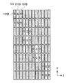
ここで、図4に、本実施の形態の比較例に係る画素配列(画素配列100A)について示す。画素配列100Aでは、1つのピクセル(画素100)内に、R,G,B,Wを発光する4つのサブピクセル(画素100R,100G,100B,100W)が、格子状に配置されている。つまり、画素100では、2×2の各領域に、画素100R,100G,100B,100Wのいずれかが配置され、画素100R,100G,100B,100Wの平面形状はいずれも略方形状となっている。
Here, FIG. 4 shows a pixel array (
図5に、このような比較例の画素配列100Aにおいて、画素100Gが発光駆動された画素列(A1,A4)と、画素100Wが発光駆動された画素列(A2,A3)とを模式的に示す。尚、画素100G,100W以外のサブピクセルについては黒色で示している。このように、画素配列100Aでは、画素100Gと画素100WとのX方向における間隔(D100a,D100b)が場所によって異なる。例えば、画素列A1,A2間では、画素100Gと画素100Wとの間隔D100aが大きくなり過ぎる一方、画素列A3,A4間では、画素100Gと画素100Wとの間隔D100bが小さくなり過ぎる。画素100G,100Wの視感度が高いことから、表示画像では、間隔D100aに対応する部分が例えば暗線として視認され、間隔D100bに対応する部分が例えば輝線として視認され易い。
FIG. 5 schematically shows a pixel column (A1, A4) in which the
これに対し、本実施の形態の画素配列Aでは、画素10R,10G,10B,10Wのうち、画素10G,10Wが、画素10内において、画素中心Pに対して対称性を有するように配置されている。
On the other hand, in the pixel array A of the present embodiment, among the
ここで、図6に、画素配列Aにおいて、画素10Gが発光駆動された画素列(A1,A4)と、画素10Wが発光駆動された画素列(A2,A3)とについて模式的に示す。このように、画素配列10Aでは、画素10G,10Wが上述したような対称性を有することにより、画素10Gと画素10WとのX方向における間隔(Dx)が略一定となる(隣接する画素列同士の間において、画素10Gと画素10Wとの間隔が略一定となる)。従って、本実施の形態では、例えば隣接する2つの画素列のそれぞれにおいて、視感度の高い画素10G,10Wを発光させた場合であっても、表示画像における、上記のような暗線(あるいは輝線)の発生が抑制される。
Here, in the pixel array A, FIG. 6 schematically illustrates a pixel column (A1, A4) in which the
また図7には、画素配列Aにおいて、画素10Gが発光駆動された画素行(B1,B4)と、画素10Wが発光駆動された画素行(B2,B3)とについて模式的に示す。このように、画素配列10Aでは、画素10G,10Wが上述したような対称性を有することにより、画素10Gと画素10WとのY方向における間隔(Dy)が略一定となる(隣接する画素行同士の間において、画素10Gと画素10Wとの間隔が略一定となる)。従って、本実施の形態では、例えば隣接する2つの画素行のそれぞれにおいて、視感度の高い画素10G,10Wを発光させた場合であっても、表示画像における、上記のような暗線(あるいは輝線)の発生が抑制される。
FIG. 7 schematically shows pixel rows (B1, B4) in which the
このように、本実施の形態では、画素10内において、輝度成分を主成分として含む色光を発する画素10G,10Wが、画素中心Pに対して対称性を有していることにより、暗線(あるいは輝線)の発生が抑制される。また、本実施の形態の画素配列Aでは、上記構成により、画素10G,10Wを発光駆動した場合に、X,Y方向の両方における間隔(Dx,Dy)が一定となることから、例えば水平方向にも垂直方向にも暗線(輝線)の抑制された表示画像が得られる。
As described above, in the present embodiment, the
また、本実施の形態では、画素配列Aにおいて、画素10R,10G,10B,10Wが全体としてストライプ状となるように配置されている。特に、画素10G,10Wは、上述したような対称性を持ちつつ、Y方向に沿った1つのラインを成すように配置されている。画素配列Aにおいて、画素10R,10G,10B,10Wが、そのようなストライプ状を成すことにより、以下に説明するような、いわゆるサブピクセルレンダリングによる表示駆動に好適な画素構造を実現できる。
In the present embodiment, in the pixel array A, the
まず、図8Aおよび図8Bを参照して、RGBのサブピクセルを用いたサブピクセルレンダリングによる表示駆動動作の概要について説明する。例えば、表示画像として、「斜め方向に沿って延在する白線」を表現する場合において、図8Aは、ピクセル単位の表示駆動動作、図8Bは、サブピクセル単位の表示駆動動作(サブピクセルレンダリング)を、それぞれ模式的に表している。また、このサブピクセルレンダリングは、例えばRGBの各サブピクセルがストライプ状に配置されている画素配列に対して行われ、画像信号Dinとしては、サブピクセルレンダリングに対応したものが用いられる。 First, with reference to FIG. 8A and FIG. 8B, an outline of a display driving operation by sub-pixel rendering using RGB sub-pixels will be described. For example, when a “white line extending along an oblique direction” is expressed as a display image, FIG. 8A shows a display drive operation in units of pixels, and FIG. 8B shows a display drive operation in units of subpixels (subpixel rendering). Are schematically represented. Further, this subpixel rendering is performed on, for example, a pixel array in which RGB subpixels are arranged in a stripe pattern, and an image signal Din corresponding to the subpixel rendering is used.
ここで、画素101(ピクセル)単位で表示駆動を行う場合には、例えば図8Aに示したように、選択的な画素101内の画素101R,101G,101B(サブピクセル)を1つの組として発光駆動する。画素101毎に白が表示され、斜めの白線が表現される。
Here, when display driving is performed in units of pixels 101 (pixels), for example, as shown in FIG. 8A, the
一方、サブピクセルレンダリングによる表示駆動を行う場合には、例えば図8Bに示したように、画素101R,101G,101Bのそれぞれを仮想的に表示単位とみなし、選択的な画素101R,101G,101Bを発光駆動する。つまり、1つの画素101を構成する画素101R,101G,101Bの組に限らず、例えば互いにX方向において隣接する画素101R,101G,101Bの並び(R,G,B)(G,B,R)(B,R,G)の各組を用いて白を表示する。これにより、図8Aに示したピクセル単位で表示駆動を行う場合よりも、解像度が向上し、斜めの白線が滑らかに表現される。
On the other hand, when performing display driving by sub-pixel rendering, for example, as shown in FIG. 8B, each of the
ところが、このようなサブピクセルレンダリングを、W画素を含む4つのサブピクセルからなる画素配列(比較例の画素配列100A)に適用した場合、次のような不具合が生じる。ここで、画素配列100Aにおいて、画素100(ピクセル)単位で表示駆動を行う場合には、例えば図9Aに示したように、選択的な画素100内の4つの画素100R,100G,100B,100W(サブピクセル)を1つの組として発光駆動する。画素100毎に白が表示され、斜めの白線が表現される。一方、例えば図8Bに示したように、画素配列100Aにおいて、画素100R,100G,100B,100Wのそれぞれを仮想的に表示単位とみなして個別に発光駆動しても、上述のRGBの3サブピクセル構成のように、滑らかな白線を表現することは困難である。
However, when such sub-pixel rendering is applied to a pixel array composed of four sub-pixels including W pixels (the
これに対し、本実施の形態の画素配列10Aでは、上述したように、画素10内において、画素10R,10G,10B,10Wが、全体としてストライプ状を成し、かつ画素10G,10Wが1ラインを成すように、配置されている。以下、このような画素配列10Aに対し、上記のような斜めの白線を表現する場合について説明する。図10Aに、画素配列10Aにおけるピクセル単位の表示駆動動作を、図10Bに、画素配列10Aにおけるサブピクセルレンダリングによる表示駆動動作を、それぞれ模式的に示す。
On the other hand, in the
図10Aに示したように、画素10(ピクセル)単位で表示駆動を行う場合には、選択的な画素10内の4つの画素10R,10G,10B,10W(サブピクセル)を1つの組として発光駆動する。
As shown in FIG. 10A, when display driving is performed in units of pixels 10 (pixels), the four
一方、図10Bに示したように、サブピクセルレンダリングによる表示駆動を行う場合には、画素10R,10G,10B,10Wのそれぞれを仮想的に表示単位とみなし、選択的な画素10R,10G,10B,10Wを発光駆動する。このように、本実施の形態では、上述したような画素配列10Aによって、上記RGBの場合(図8B)と同様のサブピクセルレンダリングを適用して、滑らかな白線を表現することができる。よって、解像度を高め、表示画質をより良好なものとすることが可能である。
On the other hand, as shown in FIG. 10B, when performing display driving by sub-pixel rendering, each of the
以上説明したように、本実施の形態では、互いに異なる発色単位(画素10R,10G,10B,10W)のうち、輝度成分を主成分として含む色光を発する画素(画素10G,10W)が、画素中心Pに対して対称性を有するように配置されている。これにより、隣接する画素行同士(または画素列同士)の間において、画素10Gと画素10Wの間隔が略一定となる。この結果、例えば高輝度化を目的として、1画素10内に画素10Wを配置した場合にも、表示画像における暗線あるいは輝線の発生を抑制できる。よって、輝度を向上させつつ表示画質の劣化を抑制することが可能となる。
As described above, in the present embodiment, among the different coloring units (
以下、上記実施の形態の画素配列Aの変形例(変形例1〜6)について説明する。尚、上記実施の形態と同様の構成要素については、同一の符号を付し、適宜説明を省略する。 Hereinafter, modified examples (modified examples 1 to 6) of the pixel array A according to the above-described embodiment will be described. In addition, about the component similar to the said embodiment, the same code | symbol is attached | subjected and description is abbreviate | omitted suitably.
<変形例1>
図11は、変形例1に係る画素配列(画素配列11A)の構成を模式的に表したものである。上記実施の形態の画素配列Aでは、画素10G,10Wをストライプ状の1ラインを成すように配置すると共に、1つの画素10Wに対して2つの画素10Gを配置した場合を例示したが、これらの画素10G,10Wの配置が逆であってもよい。即ち、本変形例のように、画素11の中央領域に、G(緑)の画素11Gが配置され、この画素11Gを挟む2箇所に、W(白)の画素11Wが配置されていてもよい。このような配置であっても、画素11内において、画素11G,11Wが上述したような対称性を有することから、上記実施の形態と同様の効果を得ることができる。
<
FIG. 11 schematically illustrates a configuration of a pixel array (
<変形例2>
図12は、変形例2に係る画素配列(画素配列12A)の構成を模式的に表したものである。上記実施の形態では、画素10R,10G,10B,10Wが全体として3つのラインからなるストライプ状を成す(画素10G,10Wが1つのラインを成す)場合を例示したが、1つのサブピクセルが1つのラインを成していてもよい。即ち、本変形例のように、画素12が、サブピクセルとして画素12R,12G,12B,12Wを有し、これらの画素12R,12G,12B,12Wのそれぞれがストライプ状の1つのラインを成してもよい。例えば、画素12R,12G,12B,12WがそれぞれY方向に沿って延在すると共に、X方向に沿って、画素12R,12G,12W,12G,12Bの順に並列配置されている。画素配列12Aでは、画素12において、2つの画素12Gの間に、1つの画素12Wが配置されている。
<
FIG. 12 schematically illustrates the configuration of a pixel array (
このような画素配列12Aにより、上述した実施の形態と同様の対称性が得られる。具体的には、画素12G,12Wが、画素中心Pに対して点対称であると共に、軸X1,Y1に対して線対称となるように配置されている。このため、本変形例においても、画素12G,12Wの輝度重心が画素中心Pと一致している。
Such a
また、画素配列12Aでは、上記のような対称性を有しつつ、全体としてストライプ状を成すように配置されているので、上述したようなサブピクセルレンダリングによる表示駆動にも好適に適用可能である。
Further, since the
更に、本変形例では、画素12R,12G,12B,12Wのそれぞれを略同一形状により形成可能であるため、カラーフィルタ等の設計が比較的容易であり、製造性の観点においても優れている。
Furthermore, in this modification, since each of the
<変形例3>
図13は、変形例3に係る画素配列(画素配列13A)の構成を模式的に表したものである。上記実施の形態では、画素10G,10Wがストライプ状におけるラインを成す場合を例示したが、上述のような所定の対称性を有していれば、必ずしもR,Bの画素と同等の幅を有していなくともよい。例えば、本変形例のように、画素13において、R(赤)の画素13Rと、青(B)の画素13Bとの間の矩形状(または方形状)の領域に、W(白)の画素13Wが配置され、この画素13Wの外周に沿って(画素13Wを囲むように)、G(緑)の画素13Gが配置されていてもよい。
<
FIG. 13 schematically illustrates the configuration of a pixel array (
このような画素配列13Aにより、上述した実施の形態と同様の対称性(画素中心Pまたは画素中心Pを通る軸に対する対称性)が得られる。また、画素配列13Aでは、画素13R,13Bと、画素13G(画素13W)との間においてライン幅が異なるものの、全体としてストライプ状を成すように配置されているので、上述したようなサブピクセルレンダリングによる表示駆動にも適用可能である。
Such a
更に、本変形例の画素配列13Aでは、画素10Gが画素10Wを取り囲むように配置され、画素10G,10Wが分離されていない(一体的な)配置であることから、例えば1本線を表示する場合等において、より自然な画像を表現可能となる。
Further, in the
<変形例4>
図14は、変形例4に係る画素配列(画素配列14A)の構成を模式的に表したものである。本変形例の画素配列14Aは、特にパターン・リターダ方式の3次元画像表示を行う際に好適に用いられるものである。このような3次元画像表示は、例えば図15に示したように、表示装置1の光出射側に、位相差フィルムであるパターン・リターダ5を配置することにより実現される。尚、図15では、表示装置1として、バックライト36と、画素配列14Aを有する表示パネル2と、偏光板4とを示している。パターン・リターダ5は、1走査線(画素行)毎に入射光線の偏光方向を変化させるフィルムであり、位相差の異なる層を交互に配列したものである。
<Modification 4>
FIG. 14 schematically illustrates the configuration of a pixel array (
画素配列14Aは、上記実施の形態と同様、画素14内に、R,G,Bの3つの画素14R,14G,14Bと共に、W(白)の画素14Wを有している。但し、本変形例では、これらのうち画素14R,14G,14Bが、例えばストライプ状を成し、画素14Wは、隣接する画素行B同士の境界付近(画素14の上部および下部)に、X方向に延在するように(X方向を長手方向とする矩形状の領域に)配置されている。
The
このような画素配列14Aにより、上述した実施の形態と同様の対称性(画素中心Pまたは画素中心Pを通る軸に対する対称性)が得られる。また、画素配列14Aでは、画素14R,14G,14Bが、全体としてストライプ状を成すように配置されているので、2次元画像表示の際には、上述したようなサブピクセルレンダリングによる表示駆動にも適用可能である。
Such a
また、本変形例の画素配列14Aは、特にパターン・リターダ方式による3次元表示表の画像と、2次元画像とを切り替えて表示する駆動を行う場合に有効である。例えば、図16に示したように、2次元画像を表示する際(2D表示時)には、各画素14において、画素14Wを発光駆動する(白表示とする)ことにより、表示画像における輝度向上が図られる。
In addition, the
一方で、3次元画像を表示する際(3D表示時)には、各画素14において、画素14Wを消灯する(黒表示とする)ことで、次のような効果を得ることができる。即ち、パターン・リターダ方式の3次元表示の際には、まず、画素配列14Aにおいて、画素行B毎に、交互に左眼用と右眼用の画像を表示する駆動がなされる。なお、左眼用および右眼用の画像は、互いに視差を有する画像である。これらの左眼用および右眼用の画像に対応する画像光のそれぞれに対し、パターン・リターダ5が、互いに異なる位相差を付与する。観察者が、所定の偏光眼鏡を用いて、パターン・リターダ5から出射した左眼用の画像光を左眼で認識すると共に、右眼用の画像光を右眼で認識することにより、立体視が実現する。
On the other hand, when displaying a three-dimensional image (at the time of 3D display), the following effects can be obtained by turning off the
ところが、このようなパターン・リターダ方式の3次元表示を行う場合、画素配列14Aでは、右眼用の画像を表示する画素行Bと、左眼用の画像を表示する画素行Bとが隣接する。このため、特に画素行B同士の境界付近から出射した、左眼用および右眼用の画像光が、パターン・リターダ5による偏光分離までの過程において、クロストークすることがある。このため、3次元表示時には、画素14Wを黒表示として、画素行B同士の境界付近を遮光することにより、左右のクロストークを抑制することができる。また、画素14Wが黒表示されることから、3次元表示時における色表現が劣化しにくいというメリットもある。
However, when performing such a pattern-retarder type three-dimensional display, in the
<変形例5>
図17は、変形例5に係る画素配列の各画素の構成を模式的に表したものである。上記実施の形態および変形例では、様々な画素配列(画素配列10A〜14A)について例示したが、本開示のサブ画素の配列は、これらのものに限定される訳ではない。即ち、輝度成分を主成分として含むサブ画素が上述したような対称性を有していれば、各サブ画素の形状、面積および位置等は自由に設定することができる。例えば、図17に示した画素15のように、W(白)の画素15Wを、画素15の中央領域に配置し、この画素15Wの外周に沿って(画素15Wを取り囲むように)、他の画素15R,15G,15Bを配置してもよい。この例においても、1つの画素15Wを挟むように、2つの画素15Gが配置されており、これによって上述した対称性が得られるようになっている。
<
FIG. 17 schematically illustrates the configuration of each pixel in the pixel array according to
<変形例6>
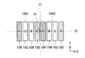
図18は、変形例6に係る画素配列(画素配列16A)の構成を模式的に表したものである。上述の実施の形態および変形例では、本開示の「単位領域」が1画素である場合を例示したが、2以上の画素からなる単位領域において、上述のような対称性を有していてもよい。即ち、本変形例のように、隣接する2つの画素16A1,16A2からなる領域を単位領域として、この画素16A1,16A2の中心P1に対して対称性を有していてもよい。
<Modification 6>
FIG. 18 schematically illustrates the configuration of a pixel array (pixel array 16A) according to Modification 6. In the above-described embodiment and modification, the case where the “unit region” of the present disclosure is one pixel is illustrated, but a unit region including two or more pixels may have the above-described symmetry. Good. That is, as in the present modification, an area composed of two adjacent pixels 16A1 and 16A2 may be used as a unit area and may have symmetry with respect to the center P1 of the pixels 16A1 and 16A2.
具体的には、画素16A1,16A2はそれぞれ、サブピクセルとして画素16R,16G,16W,16Bを有するが、これらのうち画素16G,16Wが、中心P1に対して点対称であると共に、軸X1,Y1に対して線対称となるように配置されている。本変形例では、このような構成により、画素16G,16Wの輝度重心が中心P1と一致する。
Specifically, each of the pixels 16A1 and 16A2 includes
このように、1つの画素内では対称性を有していなくとも、例えば隣接する複数の画素同士の間において対称性を有していれば、上記実施の形態に近い効果を得ることができる。 As described above, even if there is no symmetry within one pixel, for example, if there is symmetry between a plurality of adjacent pixels, an effect close to the above embodiment can be obtained.
<適用例>
以下、上記実施の形態等で説明した表示装置の適用例について説明する。上記実施の形態の表示装置1は、例えばスマートフォン、テレビジョン装置,デジタルカメラ,ノート型パーソナルコンピュータ、携帯電話等の携帯端末装置あるいはビデオカメラなど、外部から入力された映像信号あるいは内部で生成した映像信号を、画像あるいは映像として表示するあらゆる分野の電子機器の表示装置に適用することが可能である。
<Application example>
Hereinafter, application examples of the display device described in the above embodiment and the like will be described. The
図19Aおよび図19Bは、スマートフォンの外観を表している。このスマートフォンは、例えば、表示部110(表示装置1)および非表示部(筐体)120と、操作部130とを備えている。操作部130は、非表示部120の前面に設けられていてもよいし(図19A)、上面に設けられていてもよい(図19B)。
19A and 19B represent the appearance of a smartphone. This smartphone includes, for example, a display unit 110 (display device 1), a non-display unit (housing) 120, and an
図20は、テレビジョン装置の外観構成を表している。このテレビジョン装置は、例えば、フロントパネル210およびフィルターガラス220を含む映像表示画面部200(表示装置1)を備えている。 FIG. 20 illustrates an appearance configuration of a television device. The television device includes a video display screen unit 200 (display device 1) including a front panel 210 and a filter glass 220, for example.
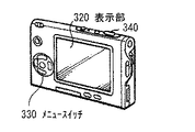
図21Aおよび図21Bは、デジタルスチルカメラの外観構成を表しており、図21Aは前面側の構成、図21Bは後面側の構成をそれぞれ示している。このデジタルスチルカメラは、例えば、フラッシュ用の発光部310と、表示部320(表示装置1)と、メニュースイッチ330と、シャッターボタン340とを備えている。
21A and 21B show the external configuration of a digital still camera, FIG. 21A shows the configuration on the front side, and FIG. 21B shows the configuration on the rear side. This digital still camera includes, for example, a light emitting unit 310 for flash, a display unit 320 (display device 1), a menu switch 330, and a
図22は、ノート型のパーソナルコンピュータの外観構成を表している。このパーソナルコンピュータは、例えば、本体410と、文字等の入力操作用のキーボード420と、画像を表示する表示部430(表示装置1)とを備えている。 FIG. 22 illustrates an appearance configuration of a notebook personal computer. The personal computer includes, for example, a main body 410, a keyboard 420 for inputting characters and the like, and a display unit 430 (display device 1) for displaying an image.
図23は、ビデオカメラの外観構成を表している。このビデオカメラは、例えば、本体部510と、その本体部510の前方側面に設けられた被写体撮影用のレンズ520と、撮影時のスタート/ストップスイッチ530と、表示部540(表示装置1)とを備えている。
FIG. 23 shows an external configuration of the video camera. This video camera includes, for example, a main body 510, a
図24は、携帯電話機の外観構成を示している。この携帯電話機は、例えば、上側筐体610と下側筐体620とが連結部(ヒンジ部)630により連結されたものであり、ディスプレイ640(表示装置1)と、サブディスプレイ650と、ピクチャーライト660と、カメラ670とを備えている。
FIG. 24 shows an external configuration of the mobile phone. In this mobile phone, for example, an
以上、実施の形態および変形例を挙げて本開示を説明したが、本開示はこれらの実施の形態等に限定されず、種々の変形が可能である。例えば、上記実施の形態等では、表示装置の一例として、液晶表示装置を例示したが、本開示は他の種類の表示装置にも適用することが可能である。具体的には、例えばPDP(Plasma Display Panel)や有機ELディスプレイなどを用いた表示装置にも適用することが可能である。 As described above, the present disclosure has been described with reference to the embodiment and the modification. However, the present disclosure is not limited to the embodiment and the like, and various modifications can be made. For example, in the above-described embodiment and the like, a liquid crystal display device is illustrated as an example of a display device, but the present disclosure can be applied to other types of display devices. Specifically, the present invention can be applied to a display device using, for example, a PDP (Plasma Display Panel) or an organic EL display.
尚、本開示内容は、以下のような構成であってもよい。
(1)
2次元配列されると共に、各々が、互いに異なる発色単位として2以上のサブ画素を含む複数の画素と、
前記複数の画素を表示駆動する駆動部と
を備え、
前記2以上のサブ画素は、輝度成分を主成分として含む色光を発する第1および第2のサブ画素を有し、
前記第1および第2のサブ画素は、1または2以上の画素からなる単位領域の中心または前記中心を通る軸に対して対称性を有するように配置されている
表示装置。
(2)
前記単位領域が1画素からなり、
前記第1および第2のサブ画素は、1画素内において前記対称性を有する
上記(1)に記載の表示装置。
(3)
前記2以上のサブ画素は、全体としてストライプ状となるように配置されている
上記(1)または(2)記載の表示装置。
(4)
前記駆動部は、表示駆動の際に、所定の画像信号を用いてサブピクセルレンダリングを行う
上記(3)に記載の表示装置。
(5)
前記第1および第2のサブ画素は、前記ストライプ状の延在方向に沿って並列配置されると共に、前記ストライプ状の1つのラインを成す
上記(3)に記載の表示装置。
(6)
前記第1および第2のサブ画素はそれぞれ、前記ストライプ状の1つのラインを成す
上記(3)に記載の表示装置。
(7)
前記第1および第2のサブ画素のうちの一方のサブ画素が、矩形状または方形状の領域に配置され、他方のサブ画素が、前記一方のサブ画素の外周に沿って配置されている
上記(3)に記載の表示装置。
(8)
前記第1および第2のサブ画素のうちの一方は、前記ストライプ状の延在方向と直交する方向に沿って、かつ隣り合う画素行同士の境界付近に配置されている
上記(3)に記載の表示装置。
(9)
前記駆動部は、2次元画像と3次元表示用の画像とを切り替えて表示可能であり、
前記3次元表示用の画像が、パターン・リターダ方式により表示される
上記(8)に記載の表示装置。
(10)
1画素内において、前記2以上のサブ画素のうち、前記第1および第2のサブ画素の一方のサブ画素が方形状または矩形状の領域に配置され、他のサブ画素が前記一方のサブ画素の外周に沿って配置されている
上記(1)に記載の表示装置。
(11)
前記単位領域が隣接する2以上の画素からなり、
前記第1および第2のサブ画素は、前記隣接する2以上の画素からなる単位領域内において、前記対称性を有する
上記(1)に記載の表示装置。
(12)
前記第1および第2のサブ画素は、白(W)、緑(G)、黄(Y)およびシアン(Cyan)のうちのいずれかの色光を発するものである
上記(1)〜(11)のいずれかに記載の表示装置。
(13)
前記第1のサブ画素は白色光を、前記第2のサブ画素は緑色光をそれぞれ発するものである
上記(12)に記載の表示装置。
(14)
2次元配列されると共に、各々が、互いに異なる発色単位として2以上のサブ画素を含む複数の画素と、
前記複数の画素を表示駆動する駆動部と
を備え、
前記2以上のサブ画素は、輝度成分を主成分として含む色光を発する第1および第2のサブ画素を有し、
前記第1および第2のサブ画素は、1または2以上の画素からなる単位領域の中心または前記中心を通る軸に対して対称性を有するように配置されている
表示装置を備えた電子機器。
Note that the present disclosure may have the following configuration.
(1)
A plurality of pixels that are two-dimensionally arranged and each include two or more sub-pixels as different coloring units;
A drive unit that drives the display of the plurality of pixels,
The two or more sub-pixels include first and second sub-pixels that emit color light including a luminance component as a main component,
The display device in which the first and second sub-pixels are arranged so as to have symmetry with respect to a center of a unit region composed of one or more pixels or an axis passing through the center.
(2)
The unit area consists of one pixel,
The display device according to (1), wherein the first and second sub-pixels have the symmetry within one pixel.
(3)
The display device according to (1) or (2), wherein the two or more sub-pixels are arranged in a stripe shape as a whole.
(4)
The display device according to (3), wherein the driving unit performs sub-pixel rendering using a predetermined image signal during display driving.
(5)
The display device according to (3), wherein the first and second sub-pixels are arranged in parallel along the stripe-shaped extending direction and form one stripe-shaped line.
(6)
The display device according to (3), wherein each of the first and second sub-pixels forms one line in the stripe shape.
(7)
One of the first and second sub-pixels is disposed in a rectangular or rectangular region, and the other sub-pixel is disposed along an outer periphery of the one sub-pixel. The display device according to (3).
(8)
One of the first and second sub-pixels is disposed in the vicinity of the boundary between adjacent pixel rows along a direction orthogonal to the stripe-shaped extending direction. Display device.
(9)
The drive unit can switch and display a two-dimensional image and a three-dimensional display image,
The display device according to (8), wherein the three-dimensional display image is displayed by a pattern retarder method.
(10)
Within one pixel, of the two or more sub-pixels, one of the first and second sub-pixels is disposed in a square or rectangular region, and the other sub-pixel is the one sub-pixel. The display device according to (1), wherein the display device is disposed along an outer periphery of the display device.
(11)
The unit region is composed of two or more adjacent pixels,
The display device according to (1), wherein the first and second sub-pixels have the symmetry in a unit region including the two or more adjacent pixels.
(12)
The first and second sub-pixels emit any color light of white (W), green (G), yellow (Y), and cyan (Cyan). (1) to (11) The display apparatus in any one of.
(13)
The display device according to (12), wherein the first sub-pixel emits white light and the second sub-pixel emits green light.
(14)
A plurality of pixels that are two-dimensionally arranged and each include two or more sub-pixels as different coloring units;
A drive unit that drives the display of the plurality of pixels,
The two or more sub-pixels include first and second sub-pixels that emit color light including a luminance component as a main component,
An electronic apparatus comprising a display device, wherein the first and second sub-pixels are arranged so as to have symmetry with respect to a center of a unit region composed of one or more pixels or an axis passing through the center.
1…表示装置、10A〜14A…画素配列、10〜15…画素、10R〜15R…画素(R)、10G〜15G…画素(G)、10B〜15B…画素(B)、10W〜15W…画素(W)、36…バックライト、64…タイミング制御部、63…バックライト駆動部、61…信号線駆動回路、62…走査線駆動回路、Din…画像信号、P…画素中心、P1…中心、X1,Y1…軸、A1〜A4…画素列、B1〜B4,B…画素行、Dx,Dy…間隔。
DESCRIPTION OF
Claims (9)
前記複数の画素を表示駆動する駆動部と
を備え、
前記2以上のサブ画素は、輝度成分を主成分として含む色光を発する第1および第2のサブ画素を有すると共に、全体としてストライプ状となるように配置され、
前記第1および第2のサブ画素は、1画素内において、中心を通ると共に互いに直交する2つの軸のそれぞれに対して、対称性を有するように配置され、
前記第1および第2のサブ画素は、前記ストライプ状の1つのラインを成し、
前記1つのライン内において、前記第1および第2のサブ画素のうちの一方のサブ画素が、他方のサブ画素を挟むように、複数配置されている
表示装置。 A plurality of pixels that are two-dimensionally arranged and each include two or more sub-pixels as different coloring units;
A drive unit that drives the display of the plurality of pixels,
The two or more sub-pixels, as well as have a first and second sub-pixel emits color light including a luminance component as the main component, is arranged so that as a whole a stripe shape,
The first and second sub-pixels are arranged to have symmetry with respect to each of two axes that pass through the center and are orthogonal to each other in one pixel ,
The first and second sub-pixels form one line in the stripe shape,
A display device in which a plurality of one subpixel of the first and second subpixels are arranged in the one line so as to sandwich the other subpixel .
請求項1に記載の表示装置。 The display device according to claim 1 , wherein the driving unit performs sub-pixel rendering using a predetermined image signal during display driving.
請求項1に記載の表示装置。 2. The display device according to claim 1, wherein the first and second sub-pixels emit any color light of white (W), green (G), yellow (Y), and cyan (Cyan). .
請求項3に記載の表示装置。 The display device according to claim 3 , wherein the first sub-pixel emits white light, and the second sub-pixel emits green light.
前記複数の画素を表示駆動する駆動部と
を備え、
前記2以上のサブ画素は、輝度成分を主成分として含む色光を発する第1および第2のサブ画素を有すると共に、全体としてストライプ状となるように配置され、
前記第1および第2のサブ画素は、1画素内において、中心を通ると共に互いに直交する2つの軸のそれぞれに対して、対称性を有するように配置され、
前記第1および第2のサブ画素のうちの一方のサブ画素が、矩形状または方形状の領域に配置され、他方のサブ画素が、前記一方のサブ画素の外周に沿って配置されている
表示装置。 A plurality of pixels that are two-dimensionally arranged and each include two or more sub-pixels as different coloring units;
A drive unit for driving the plurality of pixels to display;
With
The two or more sub-pixels have first and second sub-pixels that emit colored light containing a luminance component as a main component, and are arranged in a stripe shape as a whole.
The first and second sub-pixels are arranged to have symmetry with respect to each of two axes that pass through the center and are orthogonal to each other in one pixel,
One of the first and second subpixels is disposed in a rectangular or rectangular region, and the other subpixel is disposed along the outer periphery of the one subpixel.
Viewing equipment.
前記複数の画素を表示駆動する駆動部と
を備え、
前記2以上のサブ画素は、輝度成分を主成分として含む色光を発する第1および第2のサブ画素を有すると共に、全体としてストライプ状となるように配置され、
前記第1および第2のサブ画素は、1画素内において、中心を通ると共に互いに直交する2つの軸のそれぞれに対して、対称性を有するように配置され、
前記第1および第2のサブ画素のうちの一方は、前記ストライプ状の延在方向と直交する方向に沿って、かつ隣り合う画素行同士の境界付近に配置されている
表示装置。 A plurality of pixels that are two-dimensionally arranged and each include two or more sub-pixels as different coloring units;
A drive unit for driving the plurality of pixels to display;
With
The two or more sub-pixels have first and second sub-pixels that emit colored light containing a luminance component as a main component, and are arranged in a stripe shape as a whole.
The first and second sub-pixels are arranged to have symmetry with respect to each of two axes that pass through the center and are orthogonal to each other in one pixel,
One of the first and second sub-pixels is arranged in a direction orthogonal to the stripe-shaped extending direction and in the vicinity of a boundary between adjacent pixel rows.
Viewing equipment.
前記3次元表示用の画像が、パターン・リターダ方式により表示される
請求項6に記載の表示装置。 The drive unit can switch and display a two-dimensional image and a three-dimensional display image,
The display device according to claim 6, wherein the three-dimensional display image is displayed by a pattern retarder method.
前記複数の画素を表示駆動する駆動部と
を備え、
前記2以上のサブ画素は、輝度成分を主成分として含む色光を発する第1および第2のサブ画素を有し、
前記第1および第2のサブ画素は、1画素内において、中心を通ると共に互いに直交する2つの軸のそれぞれに対して、対称性を有するように配置され、
1画素内において、前記2以上のサブ画素のうち、前記第1および第2のサブ画素の一方のサブ画素が方形状または矩形状の領域に配置され、他のサブ画素が前記一方のサブ画素の外周に沿って配置されている
表示装置。 A plurality of pixels that are two-dimensionally arranged and each include two or more sub-pixels as different coloring units;
A drive unit for driving the plurality of pixels to display;
With
The two or more sub-pixels include first and second sub-pixels that emit color light including a luminance component as a main component,
The first and second sub-pixels are arranged to have symmetry with respect to each of two axes that pass through the center and are orthogonal to each other in one pixel,
Within one pixel, of the two or more sub-pixels, one of the first and second sub-pixels is disposed in a square or rectangular region, and the other sub-pixel is the one sub-pixel. Is arranged along the outer periphery of
Viewing equipment.
前記複数の画素を表示駆動する駆動部と
を備え、
前記2以上のサブ画素は、輝度成分を主成分として含む色光を発する第1および第2のサブ画素を有すると共に、全体としてストライプ状となるように配置され、
前記第1および第2のサブ画素は、1画素内において、中心を通ると共に互いに直交する2つの軸のそれぞれに対して、対称性を有するように配置され、
前記第1および第2のサブ画素は、前記ストライプ状の1つのラインを成し、
前記1つのライン内において、前記第1および第2のサブ画素のうちの一方のサブ画素が、他方のサブ画素を挟むように、複数配置されている
表示装置を備えた電子機器。 A plurality of pixels that are two-dimensionally arranged and each include two or more sub-pixels as different coloring units;
A drive unit that drives the display of the plurality of pixels,
The two or more sub-pixels, as well as have a first and second sub-pixel emits color light including a luminance component as the main component, is arranged so that as a whole a stripe shape,
The first and second sub-pixels are arranged to have symmetry with respect to each of two axes that pass through the center and are orthogonal to each other in one pixel ,
The first and second sub-pixels form one line in the stripe shape,
An electronic apparatus including a display device in which a plurality of one subpixel of the first and second subpixels are interposed in the one line so as to sandwich the other subpixel .
Priority Applications (4)
| Application Number | Priority Date | Filing Date | Title |
|---|---|---|---|
| JP2013027382A JP5910529B2 (en) | 2013-02-15 | 2013-02-15 | Display device and electronic device |
| US14/175,294 US20140232757A1 (en) | 2013-02-15 | 2014-02-07 | Display device and electronic apparatus |
| CN201811094963.7A CN109116610B (en) | 2013-02-15 | 2014-02-07 | Display device and electronic apparatus |
| CN201410045305.4A CN103995379B (en) | 2013-02-15 | 2014-02-07 | Display device and electronic equipment |
Applications Claiming Priority (1)
| Application Number | Priority Date | Filing Date | Title |
|---|---|---|---|
| JP2013027382A JP5910529B2 (en) | 2013-02-15 | 2013-02-15 | Display device and electronic device |
Publications (3)
| Publication Number | Publication Date |
|---|---|
| JP2014157207A JP2014157207A (en) | 2014-08-28 |
| JP2014157207A5 JP2014157207A5 (en) | 2015-04-02 |
| JP5910529B2 true JP5910529B2 (en) | 2016-04-27 |
Family
ID=51309589
Family Applications (1)
| Application Number | Title | Priority Date | Filing Date |
|---|---|---|---|
| JP2013027382A Active JP5910529B2 (en) | 2013-02-15 | 2013-02-15 | Display device and electronic device |
Country Status (3)
| Country | Link |
|---|---|
| US (1) | US20140232757A1 (en) |
| JP (1) | JP5910529B2 (en) |
| CN (2) | CN103995379B (en) |
Families Citing this family (19)
| Publication number | Priority date | Publication date | Assignee | Title |
|---|---|---|---|---|
| CN104103228B (en) * | 2014-06-25 | 2016-08-17 | 深圳市华星光电技术有限公司 | Display floater and the method for display image thereof |
| KR102244243B1 (en) * | 2014-09-12 | 2021-04-26 | 엘지디스플레이 주식회사 | Display device and display panel |
| CN104505021B (en) * | 2014-12-16 | 2017-09-22 | 利亚德光电股份有限公司 | pixel display adjusting method and device |
| JP2017040733A (en) * | 2015-08-19 | 2017-02-23 | 株式会社ジャパンディスプレイ | Display device |
| CN105093631B (en) * | 2015-08-28 | 2018-08-14 | 厦门天马微电子有限公司 | Dot structure, array substrate, display device and sub-pixel rendering intent |
| CN106486513B (en) * | 2015-08-31 | 2023-09-29 | 昆山国显光电有限公司 | Pixel structure and OLED display panel |
| CN111326121B (en) * | 2018-12-13 | 2021-11-16 | 京东方科技集团股份有限公司 | Driving method, driving chip, display device and storage medium |
| CN106652909A (en) * | 2017-02-27 | 2017-05-10 | 昆山国显光电有限公司 | Pixel structure and display device |
| CN109003577B (en) * | 2017-06-07 | 2020-05-12 | 京东方科技集团股份有限公司 | Driving method and assembly of display panel, display device, terminal and storage medium |
| CN107024795B (en) | 2017-06-19 | 2020-03-20 | 上海天马微电子有限公司 | Display panel and display device |
| CN107219693B (en) * | 2017-07-28 | 2020-09-08 | 厦门天马微电子有限公司 | Display panel and display device |
| CN107621716B (en) * | 2017-09-28 | 2020-08-11 | 武汉天马微电子有限公司 | Pixel structure, driving method thereof, display panel and display device |
| CN107633809B (en) * | 2017-09-30 | 2019-05-21 | 京东方科技集团股份有限公司 | Eliminate method, display screen and the display device of more IC driving display screen concealed wires |
| CN107817625B (en) * | 2017-10-11 | 2020-10-09 | 深圳市华星光电半导体显示技术有限公司 | Pixel structure, color film substrate and display panel |
| US10690822B2 (en) | 2017-10-11 | 2020-06-23 | Shenzhen China Star Optoelectronics Semiconductor Display Technology Co., Ltd. | Pixel structure, color filter substrate, and display panel |
| CN111613165B (en) * | 2019-02-23 | 2022-09-09 | 华为技术有限公司 | Method and electronic device for displaying image in multi-display driving circuit system |
| CN116564209A (en) | 2019-02-23 | 2023-08-08 | 华为技术有限公司 | Method and electronic device for displaying images in multi-display driving circuit system |
| CN110060619B (en) * | 2019-04-24 | 2022-05-10 | 格兰菲智能科技有限公司 | Sub-pixel rendering method and device |
| CN110047417B (en) * | 2019-04-24 | 2022-05-17 | 格兰菲智能科技有限公司 | Sub-pixel rendering method and device |
Family Cites Families (67)
| Publication number | Priority date | Publication date | Assignee | Title |
|---|---|---|---|---|
| JPS60218626A (en) * | 1984-04-13 | 1985-11-01 | Sharp Corp | Color llquid crystal display device |
| US5642176A (en) * | 1994-11-28 | 1997-06-24 | Canon Kabushiki Kaisha | Color filter substrate and liquid crystal display device |
| JPH11212060A (en) * | 1998-01-26 | 1999-08-06 | Sharp Corp | Liquid crystal display device |
| US6100861A (en) * | 1998-02-17 | 2000-08-08 | Rainbow Displays, Inc. | Tiled flat panel display with improved color gamut |
| US7274383B1 (en) * | 2000-07-28 | 2007-09-25 | Clairvoyante, Inc | Arrangement of color pixels for full color imaging devices with simplified addressing |
| JP3960762B2 (en) * | 2001-07-19 | 2007-08-15 | シャープ株式会社 | Display device and manufacturing method thereof |
| JP3941548B2 (en) * | 2002-03-06 | 2007-07-04 | セイコーエプソン株式会社 | Liquid crystal display panel, liquid crystal display panel substrate and electronic device |
| CN1324363C (en) * | 2002-05-04 | 2007-07-04 | 三星电子株式会社 | LCD device and filtering color picec array board |
| US6888604B2 (en) * | 2002-08-14 | 2005-05-03 | Samsung Electronics Co., Ltd. | Liquid crystal display |
| JP3796499B2 (en) * | 2002-11-06 | 2006-07-12 | キヤノン株式会社 | Color display element, color display element driving method, and color display device |
| US6919681B2 (en) * | 2003-04-30 | 2005-07-19 | Eastman Kodak Company | Color OLED display with improved power efficiency |
| US7495722B2 (en) * | 2003-12-15 | 2009-02-24 | Genoa Color Technologies Ltd. | Multi-color liquid crystal display |
| KR20050064176A (en) * | 2003-12-23 | 2005-06-29 | 엘지.필립스 엘시디 주식회사 | Liquid crystal display device |
| KR101072375B1 (en) * | 2003-12-29 | 2011-10-11 | 엘지디스플레이 주식회사 | Liquid Crystal Display Device Automatically Adjusting Aperture Ratio In Each Pixel |
| WO2005101807A2 (en) * | 2004-04-09 | 2005-10-27 | Clairvoyante, Inc. | Novel subpixel layouts and arrangements for high brightness displays |
| KR20050113907A (en) * | 2004-05-31 | 2005-12-05 | 삼성전자주식회사 | Liquid crystal display device and driving method for the same |
| US7515122B2 (en) * | 2004-06-02 | 2009-04-07 | Eastman Kodak Company | Color display device with enhanced pixel pattern |
| KR101041970B1 (en) * | 2004-06-11 | 2011-06-16 | 삼성전자주식회사 | Liquid crystal display device |
| KR101148791B1 (en) * | 2004-06-30 | 2012-05-24 | 엘지디스플레이 주식회사 | Tiled display device |
| JP4123208B2 (en) * | 2004-09-03 | 2008-07-23 | セイコーエプソン株式会社 | Liquid crystal display device, electronic equipment |
| JP2008076416A (en) * | 2004-12-27 | 2008-04-03 | Sharp Corp | Driving device for display panel, display panel, display device with the same, and driving method for display panel |
| JP4823571B2 (en) * | 2005-05-30 | 2011-11-24 | 株式会社 日立ディスプレイズ | 3D display device |
| JP4120674B2 (en) * | 2005-09-09 | 2008-07-16 | エプソンイメージングデバイス株式会社 | Electro-optical device and electronic apparatus |
| JP2007094089A (en) * | 2005-09-29 | 2007-04-12 | Sanyo Epson Imaging Devices Corp | Electrooptical device and electronic equipment |
| CN100510924C (en) * | 2005-11-09 | 2009-07-08 | 株式会社普利司通 | Information display panel |
| KR20070070721A (en) * | 2005-12-29 | 2007-07-04 | 엘지.필립스 엘시디 주식회사 | Liquid crystal display device and driving method thereof |
| WO2007088656A1 (en) * | 2006-02-02 | 2007-08-09 | Sharp Kabushiki Kaisha | Display |
| KR20070081924A (en) * | 2006-02-14 | 2007-08-20 | 삼성전자주식회사 | Display apparatus |
| KR101290168B1 (en) * | 2006-06-30 | 2013-07-30 | 엘지디스플레이 주식회사 | Transflective liquid crystal display device |
| US8018476B2 (en) * | 2006-08-28 | 2011-09-13 | Samsung Electronics Co., Ltd. | Subpixel layouts for high brightness displays and systems |
| JP5403860B2 (en) * | 2006-10-10 | 2014-01-29 | 株式会社ジャパンディスプレイ | Color liquid crystal display device |
| JP4349456B2 (en) * | 2006-10-23 | 2009-10-21 | ソニー株式会社 | Solid-state image sensor |
| JP2008233803A (en) * | 2007-03-23 | 2008-10-02 | Casio Comput Co Ltd | Display device |
| TWI368456B (en) * | 2007-04-20 | 2012-07-11 | Au Optronics Corp | Organic electro-luminescence display |
| JP2009122401A (en) * | 2007-11-15 | 2009-06-04 | Toppoly Optoelectronics Corp | Active matrix display device |
| KR101471547B1 (en) * | 2008-02-20 | 2014-12-11 | 삼성디스플레이 주식회사 | Liquid crystal display |
| JP4582195B2 (en) * | 2008-05-29 | 2010-11-17 | ソニー株式会社 | Display device |
| KR100947453B1 (en) * | 2008-06-18 | 2010-03-11 | 삼성모바일디스플레이주식회사 | Pixel structure of Organic Light Emitting Display |
| JP2010210712A (en) * | 2009-03-06 | 2010-09-24 | Sony Corp | Image display apparatus, image display observation system, and image display method |
| KR101560236B1 (en) * | 2009-08-28 | 2015-10-15 | 엘지디스플레이 주식회사 | liquid crystal display |
| KR101568262B1 (en) * | 2009-09-08 | 2015-11-12 | 엘지디스플레이 주식회사 | 4 liquid crystal display with 4 color subpixels |
| EP2503385A1 (en) * | 2009-11-19 | 2012-09-26 | Sharp Kabushiki Kaisha | Liquid crystal display device and manufacturing method therefor |
| KR101634744B1 (en) * | 2009-12-30 | 2016-07-11 | 삼성디스플레이 주식회사 | Display apparatus |
| WO2011092915A1 (en) * | 2010-01-28 | 2011-08-04 | シャープ株式会社 | Display device |
| CN102725681B (en) * | 2010-01-29 | 2015-01-28 | 夏普株式会社 | Liquid crystal display device |
| CN102754443B (en) * | 2010-02-12 | 2014-11-12 | 佳能株式会社 | Image processing device and image processing method |
| JP5650918B2 (en) * | 2010-03-26 | 2015-01-07 | 株式会社ジャパンディスプレイ | Image display device |
| WO2012005170A1 (en) * | 2010-07-06 | 2012-01-12 | シャープ株式会社 | Multiple-primary color liquid crystal display apparatus |
| CN103155026B (en) * | 2010-10-19 | 2015-09-23 | 夏普株式会社 | Display device |
| WO2012070469A1 (en) * | 2010-11-24 | 2012-05-31 | シャープ株式会社 | Stereoscopic display device |
| TW201225034A (en) * | 2010-12-02 | 2012-06-16 | Himax Display Inc | Color filter arrangement for display panel |
| US8455160B2 (en) * | 2010-12-09 | 2013-06-04 | Himax Technologies Limited | Color filter of liquid crystal on silicon display device |
| KR20120066323A (en) * | 2010-12-14 | 2012-06-22 | 엘지디스플레이 주식회사 | In-plane switching mode liquid crystal display device and method of fabricating color filter substrate for in-plane switching mode liquid crystal display device |
| KR20120076860A (en) * | 2010-12-30 | 2012-07-10 | 엘지디스플레이 주식회사 | Liquid crystal display device |
| US9183797B2 (en) * | 2011-04-13 | 2015-11-10 | Sharp Kabushiki Kaisha | Display device and control method for display device |
| CN202041673U (en) * | 2011-05-09 | 2011-11-16 | 京东方科技集团股份有限公司 | Color filter and liquid crystal display |
| TW201248214A (en) * | 2011-05-16 | 2012-12-01 | E Ink Holdings Inc | Color filter applications thereof and method for manufacturing the same |
| KR20120138205A (en) * | 2011-06-14 | 2012-12-24 | 삼성디스플레이 주식회사 | Display device |
| CN202189508U (en) * | 2011-06-17 | 2012-04-11 | 深圳晶为华悦科技有限公司 | Color display screen |
| CN202141871U (en) * | 2011-07-13 | 2012-02-08 | 京东方科技集团股份有限公司 | Display panel and display device |
| KR101852936B1 (en) * | 2011-08-31 | 2018-04-30 | 삼성디스플레이 주식회사 | Display device |
| GB2496113A (en) * | 2011-10-28 | 2013-05-08 | Sharp Kk | Multiple view window multi-primary display |
| JP2013140209A (en) * | 2011-12-28 | 2013-07-18 | Panasonic Liquid Crystal Display Co Ltd | Liquid crystal display device |
| CN202512325U (en) * | 2012-01-06 | 2012-10-31 | 京东方科技集团股份有限公司 | Four-color pixel structure, four-color liquid crystal display panel, array substrate and color film substrate |
| CN102779495B (en) * | 2012-04-05 | 2015-09-09 | 北京京东方光电科技有限公司 | A kind of display panels and drive unit, method |
| JP5702894B2 (en) * | 2012-07-06 | 2015-04-15 | 富士フイルム株式会社 | Color imaging device and imaging apparatus |
| CN202736924U (en) * | 2012-08-01 | 2013-02-13 | Tcl集团股份有限公司 | Pixel structure, display panel and display |
-
2013
- 2013-02-15 JP JP2013027382A patent/JP5910529B2/en active Active
-
2014
- 2014-02-07 CN CN201410045305.4A patent/CN103995379B/en active Active
- 2014-02-07 US US14/175,294 patent/US20140232757A1/en not_active Abandoned
- 2014-02-07 CN CN201811094963.7A patent/CN109116610B/en active Active
Also Published As
| Publication number | Publication date |
|---|---|
| CN103995379B (en) | 2018-10-19 |
| CN109116610A (en) | 2019-01-01 |
| CN109116610B (en) | 2022-07-12 |
| US20140232757A1 (en) | 2014-08-21 |
| JP2014157207A (en) | 2014-08-28 |
| CN103995379A (en) | 2014-08-20 |
Similar Documents
| Publication | Publication Date | Title |
|---|---|---|
| JP5910529B2 (en) | Display device and electronic device | |
| US7876350B2 (en) | Three-dimensional image display | |
| US9122065B2 (en) | Display panel, display and electronic device | |
| CN105911785B (en) | A kind of display panel and display device | |
| WO2013042332A1 (en) | Video display method, video display panel, and video display apparatus | |
| US20130241964A1 (en) | Display device and electronic apparatus | |
| KR20210009368A (en) | Pixel arrangement structure, display panel and display device | |
| JP2014525054A (en) | Display panel and display device | |
| WO2017028439A1 (en) | 3d display apparatus and driving method therefor | |
| KR20070118079A (en) | Autostereoscopic display apparatus and colour filter therefor | |
| WO2017092708A1 (en) | 3d imaging device and a driving method thereof | |
| US20120229457A1 (en) | Display device | |
| WO2017059681A1 (en) | Pixel structure, fabrication method thereof, display panel, and display apparatus | |
| JP2008197132A (en) | Directional display | |
| US20160247433A1 (en) | Display panel, display method and display device | |
| JP2012118538A (en) | Color display device, liquid crystal display device, and transflective liquid crystal display device | |
| JP2016126337A (en) | Display device and driving method of the same | |
| US10613344B2 (en) | 3D display apparatus and method for driving the 3D display apparatus | |
| JP2017044768A (en) | Display device and head-mounted display device | |
| US8547297B1 (en) | Enhanced color resolution display screen using pixel shifting | |
| JP2013200571A (en) | Liquid crystal display device and transflective liquid crystal display device | |
| JP2013211147A (en) | Display device | |
| CN110262120B (en) | Substrate, preparation method thereof and display panel | |
| CN109581723B (en) | Display panel and display device | |
| JP2005128190A (en) | Device for display and image display apparatus |
Legal Events
| Date | Code | Title | Description |
|---|---|---|---|
| A521 | Request for written amendment filed |
Free format text: JAPANESE INTERMEDIATE CODE: A523 Effective date: 20150213 |
|
| A621 | Written request for application examination |
Free format text: JAPANESE INTERMEDIATE CODE: A621 Effective date: 20150213 |
|
| A977 | Report on retrieval |
Free format text: JAPANESE INTERMEDIATE CODE: A971007 Effective date: 20150610 |
|
| A131 | Notification of reasons for refusal |
Free format text: JAPANESE INTERMEDIATE CODE: A131 Effective date: 20150630 |
|
| A521 | Request for written amendment filed |
Free format text: JAPANESE INTERMEDIATE CODE: A523 Effective date: 20150731 |
|
| A131 | Notification of reasons for refusal |
Free format text: JAPANESE INTERMEDIATE CODE: A131 Effective date: 20151222 |
|
| A521 | Request for written amendment filed |
Free format text: JAPANESE INTERMEDIATE CODE: A523 Effective date: 20160119 |
|
| TRDD | Decision of grant or rejection written | ||
| A01 | Written decision to grant a patent or to grant a registration (utility model) |
Free format text: JAPANESE INTERMEDIATE CODE: A01 Effective date: 20160301 |
|
| A61 | First payment of annual fees (during grant procedure) |
Free format text: JAPANESE INTERMEDIATE CODE: A61 Effective date: 20160314 |
|
| R151 | Written notification of patent or utility model registration |
Ref document number: 5910529 Country of ref document: JP Free format text: JAPANESE INTERMEDIATE CODE: R151 |
|
| R250 | Receipt of annual fees |
Free format text: JAPANESE INTERMEDIATE CODE: R250 |
|
| R250 | Receipt of annual fees |
Free format text: JAPANESE INTERMEDIATE CODE: R250 |