JP6480669B2 - Display device, display device driving method, and electronic apparatus - Google Patents
Display device, display device driving method, and electronic apparatus Download PDFInfo
- Publication number
- JP6480669B2 JP6480669B2 JP2014084041A JP2014084041A JP6480669B2 JP 6480669 B2 JP6480669 B2 JP 6480669B2 JP 2014084041 A JP2014084041 A JP 2014084041A JP 2014084041 A JP2014084041 A JP 2014084041A JP 6480669 B2 JP6480669 B2 JP 6480669B2
- Authority
- JP
- Japan
- Prior art keywords
- subpixel
- value
- signal
- pixel
- sub
- Prior art date
- Legal status (The legal status is an assumption and is not a legal conclusion. Google has not performed a legal analysis and makes no representation as to the accuracy of the status listed.)
- Active
Links
- 238000000034 method Methods 0.000 title claims description 44
- 238000012937 correction Methods 0.000 claims description 91
- 238000012545 processing Methods 0.000 claims description 78
- 238000005286 illumination Methods 0.000 claims 2
- 230000000052 comparative effect Effects 0.000 description 52
- 238000010586 diagram Methods 0.000 description 41
- 230000006837 decompression Effects 0.000 description 17
- 239000004973 liquid crystal related substance Substances 0.000 description 14
- 230000007423 decrease Effects 0.000 description 9
- 230000006866 deterioration Effects 0.000 description 9
- 238000011156 evaluation Methods 0.000 description 8
- 230000007274 generation of a signal involved in cell-cell signaling Effects 0.000 description 5
- 230000015556 catabolic process Effects 0.000 description 3
- 238000006731 degradation reaction Methods 0.000 description 3
- 239000011159 matrix material Substances 0.000 description 3
- 239000000470 constituent Substances 0.000 description 2
- 239000000446 fuel Substances 0.000 description 2
- 230000001678 irradiating effect Effects 0.000 description 2
- 238000012986 modification Methods 0.000 description 2
- 230000004048 modification Effects 0.000 description 2
- 239000011347 resin Substances 0.000 description 2
- 229920005989 resin Polymers 0.000 description 2
- 239000007787 solid Substances 0.000 description 2
- XLYOFNOQVPJJNP-UHFFFAOYSA-N water Substances O XLYOFNOQVPJJNP-UHFFFAOYSA-N 0.000 description 2
- 238000006243 chemical reaction Methods 0.000 description 1
- 239000003086 colorant Substances 0.000 description 1
- 230000006835 compression Effects 0.000 description 1
- 238000007906 compression Methods 0.000 description 1
- 230000003247 decreasing effect Effects 0.000 description 1
- 239000011521 glass Substances 0.000 description 1
- 230000011664 signaling Effects 0.000 description 1
- 238000006467 substitution reaction Methods 0.000 description 1
- 238000002834 transmittance Methods 0.000 description 1
- 230000000007 visual effect Effects 0.000 description 1
Images


Classifications
-
- G—PHYSICS
- G09—EDUCATION; CRYPTOGRAPHY; DISPLAY; ADVERTISING; SEALS
- G09G—ARRANGEMENTS OR CIRCUITS FOR CONTROL OF INDICATING DEVICES USING STATIC MEANS TO PRESENT VARIABLE INFORMATION
- G09G5/00—Control arrangements or circuits for visual indicators common to cathode-ray tube indicators and other visual indicators
- G09G5/02—Control arrangements or circuits for visual indicators common to cathode-ray tube indicators and other visual indicators characterised by the way in which colour is displayed
-
- G—PHYSICS
- G09—EDUCATION; CRYPTOGRAPHY; DISPLAY; ADVERTISING; SEALS
- G09G—ARRANGEMENTS OR CIRCUITS FOR CONTROL OF INDICATING DEVICES USING STATIC MEANS TO PRESENT VARIABLE INFORMATION
- G09G3/00—Control arrangements or circuits, of interest only in connection with visual indicators other than cathode-ray tubes
- G09G3/20—Control arrangements or circuits, of interest only in connection with visual indicators other than cathode-ray tubes for presentation of an assembly of a number of characters, e.g. a page, by composing the assembly by combination of individual elements arranged in a matrix no fixed position being assigned to or needed to be assigned to the individual characters or partial characters
- G09G3/34—Control arrangements or circuits, of interest only in connection with visual indicators other than cathode-ray tubes for presentation of an assembly of a number of characters, e.g. a page, by composing the assembly by combination of individual elements arranged in a matrix no fixed position being assigned to or needed to be assigned to the individual characters or partial characters by control of light from an independent source
- G09G3/36—Control arrangements or circuits, of interest only in connection with visual indicators other than cathode-ray tubes for presentation of an assembly of a number of characters, e.g. a page, by composing the assembly by combination of individual elements arranged in a matrix no fixed position being assigned to or needed to be assigned to the individual characters or partial characters by control of light from an independent source using liquid crystals
- G09G3/3611—Control of matrices with row and column drivers
-
- G—PHYSICS
- G09—EDUCATION; CRYPTOGRAPHY; DISPLAY; ADVERTISING; SEALS
- G09G—ARRANGEMENTS OR CIRCUITS FOR CONTROL OF INDICATING DEVICES USING STATIC MEANS TO PRESENT VARIABLE INFORMATION
- G09G2340/00—Aspects of display data processing
- G09G2340/04—Changes in size, position or resolution of an image
- G09G2340/0457—Improvement of perceived resolution by subpixel rendering
-
- G—PHYSICS
- G09—EDUCATION; CRYPTOGRAPHY; DISPLAY; ADVERTISING; SEALS
- G09G—ARRANGEMENTS OR CIRCUITS FOR CONTROL OF INDICATING DEVICES USING STATIC MEANS TO PRESENT VARIABLE INFORMATION
- G09G2340/00—Aspects of display data processing
- G09G2340/06—Colour space transformation
Landscapes
- Engineering & Computer Science (AREA)
- Physics & Mathematics (AREA)
- Computer Hardware Design (AREA)
- General Physics & Mathematics (AREA)
- Theoretical Computer Science (AREA)
- Chemical & Material Sciences (AREA)
- Crystallography & Structural Chemistry (AREA)
- Control Of Indicators Other Than Cathode Ray Tubes (AREA)
- Liquid Crystal Display Device Control (AREA)
- Liquid Crystal (AREA)
Description
本開示は、表示装置、その駆動方法及びその表示装置を備えた電子機器に関する。 The present disclosure relates to a display device, a driving method thereof, and an electronic apparatus including the display device.
近年、携帯電話及び電子ペーパー等のモバイル機器向け等の表示装置の需要が高くなっている。表示装置では、1つの画素が複数の副画素を備え、当該複数の副画素がそれぞれ異なる色の光を出力し、当該副画素の表示のON、OFFを切り換えることで、1つの画素で種々の色を表示させている。このような表示装置は、解像度及び輝度といった表示特性も年々向上してきている。しかし、解像度が高くなるにしたがって開口率が低下してくるため、高輝度を達成しようとした場合、バックライトの輝度を高くする必要があり、バックライトの消費電力が増大するという問題がある。これを改善するため、従来の赤、緑、青の副画素に第4の副画素である白画素を加える技術がある(例えば、特許文献1)。この技術は、白画素が輝度を向上させる分、バックライトの電流値を下げ、消費電力を低減する。 In recent years, the demand for display devices for mobile devices such as mobile phones and electronic paper has increased. In a display device, one pixel includes a plurality of sub-pixels, each of the plurality of sub-pixels outputs light of a different color, and the display of the sub-pixel is switched on and off, whereby one pixel can perform various operations. The color is displayed. Such display devices have improved display characteristics such as resolution and luminance year by year. However, since the aperture ratio decreases as the resolution increases, there is a problem that, when trying to achieve high luminance, it is necessary to increase the luminance of the backlight, and the power consumption of the backlight increases. In order to improve this, there is a technique of adding a white pixel as a fourth subpixel to a conventional red, green, and blue subpixel (for example, Patent Document 1). This technology reduces the current value of the backlight and the power consumption by the amount that the white pixel improves the luminance.
ここで、白画素は赤、緑、青画素等の他の色画素よりも輝度が高い。従って、白画素と隣接する他の色画素との輝度差が大きい場合、白画素と隣接する他の色画素との間の境界が視認され、画質が劣化する可能性がある。 Here, the white pixels have higher luminance than other color pixels such as red, green, and blue pixels. Therefore, when the luminance difference between the white pixel and another adjacent color pixel is large, a boundary between the white pixel and another adjacent color pixel is visually recognized, and the image quality may be deteriorated.
本発明は、画質の劣化を抑制する表示装置、表示装置の駆動方法及び電子機器を提供することを目的とする。 An object of the present invention is to provide a display device, a display device driving method, and an electronic apparatus that suppress deterioration in image quality.
本発明の表示装置は、第1の色を表示する第1副画素、第2の色を表示する第2副画素、第3の色を表示する第3副画素及び第4の色を表示する第4副画素を含む画素を複数有する画像表示パネルと、入力信号の入力値を、前記第1の色、前記第2の色、前記第3の色及び前記第4の色で再現される再現色空間の再現値に変換して生成し、生成した出力信号を前記画像表示パネルに出力する信号処理部と、を有し、前記信号処理部は、前記画像表示パネルに関する伸長係数を決定し、前記第1副画素の出力信号を、少なくとも前記第1副画素の入力信号及び前記伸長係数に基づいて求めて前記第1副画素に出力し、前記第2副画素の出力信号を、少なくとも前記第2副画素の入力信号及び前記伸長係数に基づいて求めて前記第2副画素に出力し、前記第3副画素の出力信号を、少なくとも前記第3副画素の入力信号及び前記伸長係数に基づいて求めて前記第3副画素に出力し、前記第4副画素の出力信号の補正値である第4副画素補正値を、前記第1副画素の入力信号、前記第2副画素の入力信号、前記第3副画素の入力信号及び前記伸長係数に基づいて求め、前記第4副画素の出力信号を、前記第1副画素の入力信号、前記第2副画素の入力信号、前記第3副画素の入力信号、前記伸長係数及び前記第4副画素補正値に基づいて求めて前記第4副画素に出力する。 The display device of the present invention displays a first subpixel that displays a first color, a second subpixel that displays a second color, a third subpixel that displays a third color, and a fourth color. An image display panel having a plurality of pixels including a fourth sub-pixel, and a reproduction in which an input value of an input signal is reproduced in the first color, the second color, the third color, and the fourth color A signal processing unit that converts and generates a color space reproduction value and outputs the generated output signal to the image display panel, and the signal processing unit determines an expansion coefficient for the image display panel, The output signal of the first subpixel is obtained based on at least the input signal of the first subpixel and the expansion coefficient, and is output to the first subpixel, and the output signal of the second subpixel is at least the first subpixel. Obtained based on the input signal of the two sub-pixels and the expansion coefficient and output to the second sub-pixel The output signal of the third sub-pixel is obtained based on at least the input signal of the third sub-pixel and the expansion coefficient and output to the third sub-pixel, and the output value of the output signal of the fourth sub-pixel is used as a correction value. A fourth sub-pixel correction value is obtained based on the input signal of the first sub-pixel, the input signal of the second sub-pixel, the input signal of the third sub-pixel, and the expansion coefficient. An output signal is obtained based on the input signal of the first subpixel, the input signal of the second subpixel, the input signal of the third subpixel, the expansion coefficient, and the fourth subpixel correction value. Output to sub-pixel.
本発明の電子機器は、前記表示装置と、前記表示装置に前記入力信号を供給する制御装置と、を有する。 The electronic apparatus of the present invention includes the display device and a control device that supplies the input signal to the display device.
本発明の表示装置の駆動方法は、第1の色を表示する第1副画素、第2の色を表示する第2副画素、第3の色を表示する第3副画素及び第4の色を表示する第4副画素を含む画素を複数有する画像表示パネルを有する表示装置の駆動方法であって、前記第1副画素、前記第2副画素、前記第3副画素及び前記第4副画素それぞれの出力信号を求めるステップと、前記出力信号に基づいて、前記第1副画素、前記第2副画素、前記第3副画素及び前記第4副画素の動作を制御するステップと、を含み、前記出力信号を求めるステップにおいては、前記画像表示パネルに関する伸長係数を決定し、前記第1副画素の出力信号を、少なくとも前記第1副画素の入力信号及び前記伸長係数に基づいて求め、前記第2副画素の出力信号を、少なくとも前記第2副画素の入力信号及び前記伸長係数に基づいて求め、前記第3副画素の出力信号を、少なくとも前記第3副画素の入力信号及び前記伸長係数に基づいて求め、前記第4副画素の出力信号の補正値である第4副画素補正値を、前記第1副画素の入力信号、前記第2副画素の入力信号、前記第3副画素の入力信号及び前記伸長係数に基づいて求め、前記第4副画素の出力信号を、前記第1副画素の入力信号、前記第2副画素の入力信号、前記第3副画素の入力信号、前記伸長係数及び前記第4副画素補正値に基づいて求める。 The display device driving method of the present invention includes a first sub-pixel displaying a first color, a second sub-pixel displaying a second color, a third sub-pixel displaying a third color, and a fourth color. A display device driving method including an image display panel including a plurality of pixels including a fourth sub-pixel that displays the first sub-pixel, the second sub-pixel, the third sub-pixel, and the fourth sub-pixel Obtaining each output signal, and controlling the operation of the first subpixel, the second subpixel, the third subpixel, and the fourth subpixel based on the output signal, In the step of obtaining the output signal, an expansion coefficient for the image display panel is determined, an output signal of the first subpixel is obtained based on at least the input signal of the first subpixel and the expansion coefficient, 2 sub-pixel output signals at least before Obtaining the output signal of the third subpixel based on at least the input signal of the third subpixel and the expansion coefficient, and obtaining the output signal of the fourth subpixel. A fourth subpixel correction value that is a correction value of the output signal is obtained based on the input signal of the first subpixel, the input signal of the second subpixel, the input signal of the third subpixel, and the expansion coefficient, The output signal of the fourth subpixel is based on the input signal of the first subpixel, the input signal of the second subpixel, the input signal of the third subpixel, the expansion coefficient, and the fourth subpixel correction value. Ask.
以下に、本発明の各実施の形態について、図面を参照しつつ説明する。なお、開示はあくまで一例にすぎず、当業者において、発明の主旨を保っての適宜変更について容易に想到し得るものについては、当然に本発明の範囲に含有されるものである。また、図面は説明をより明確にするため、実際の態様に比べ、各部の幅、厚さ、形状等について模式的に表される場合があるが、あくまで一例であって、本発明の解釈を限定するものではない。また、本明細書と各図において、既出の図に関して前述したものと同様の要素には、同一の符号を付して、詳細な説明を適宜省略することがある。 Hereinafter, embodiments of the present invention will be described with reference to the drawings. It should be noted that the disclosure is merely an example, and those skilled in the art can easily conceive of appropriate modifications while maintaining the gist of the invention are naturally included in the scope of the present invention. In addition, for the sake of clarity, the drawings may be schematically represented with respect to the width, thickness, shape, etc. of each part as compared to the actual embodiment, but are merely examples, and the interpretation of the present invention is not limited. It is not limited. In addition, in the present specification and each drawing, elements similar to those described above with reference to the previous drawings are denoted by the same reference numerals, and detailed description may be omitted as appropriate.
(表示装置の構成)
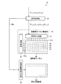
図1は、本実施形態に係る表示装置の構成の一例を示すブロック図である。図2は、本実施形態に係る画像表示パネルの画素配列を示す図である。図3は、本実施形態に係る画像表示パネル及び画像表示パネル駆動部の概念図である。図1に示すように、本実施形態の表示装置10は、信号処理部20と、画像表示パネル駆動部30と、画像表示パネル40と、面状光源装置制御部50と、面状光源装置60とを有する。表示装置10は、信号処理部20が表示装置10の各部に信号を送り、画像表示パネル駆動部30が信号処理部20からの信号に基づいて画像表示パネル40の駆動を制御し、画像表示パネル40が画像表示パネル駆動部30からの信号に基づいて画像を表示させ、面状光源装置制御部50が、信号処理部20からの信号に基づいて面状光源装置60の駆動を制御し、面状光源装置60が面状光源装置制御部50の信号に基づいて画像表示パネル40を背面から照明することにより、画像を表示する。なお、表示装置10は、特開2011−154323号公報に記載されている画像表示装置組立体と同様の構成であり、特開2011−154323号公報に記載されている各種変形例が適用可能である。
(Configuration of display device)
FIG. 1 is a block diagram illustrating an example of a configuration of a display device according to the present embodiment. FIG. 2 is a diagram showing a pixel array of the image display panel according to the present embodiment. FIG. 3 is a conceptual diagram of the image display panel and the image display panel driving unit according to the present embodiment. As shown in FIG. 1, the
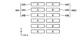
図2、図3に示すように、画像表示パネル40は、画素48が、P0×Q0個(行方向にP0個、列方向にQ0個)、2次元のマトリクス状に配列されている。図2、図3に示す例は、XYの2次元座標系に複数の画素48がマトリクス状に配列されている例を示している。この例において、行方向がX軸方向、列方向はY軸方向である。なお、行方向をY軸方向、列方向をX軸方向としてもよい。
As shown in FIGS. 2 and 3, the
画素48は、第1副画素49Rと、第2副画素49Gと、第3副画素49B又は第4副画素49Wとを有する。第1副画素49Rは、第1原色(例えば、赤色)を表示する。第2副画素49Gは、第2原色(例えば、緑色)を表示する。第3副画素49Bは、第3原色(例えば、青色)を表示する。第4副画素49Wは、第4の色(例えば、白色)を表示する。以下において、第1副画素49Rと、第2副画素49Gと、第3副画素49Bと、第4副画素49Wとをそれぞれ区別する必要がない場合、副画素49という。
The
表示装置10は、より具体的には、透過型のカラー液晶表示装置である。画像表示パネル40は、カラー液晶表示パネルであり、第1副画素49Rと画像観察者との間に第1原色を通過させる第1カラーフィルタが配置され、第2副画素49Gと画像観察者との間に第2原色を通過させる第2カラーフィルタが配置され、第3副画素49Bと画像観察者との間に第3原色を通過させる第3カラーフィルタが配置されている。また、画像表示パネル40は、第4副画素49Wと画像観察者との間にカラーフィルタが配置されていない。第4副画素49Wには、カラーフィルタの代わりに透明な樹脂層が備えられていてもよい。このように画像表示パネル40は、透明な樹脂層を設けることで、第4副画素49Wにカラーフィルタを設けないことによって第4副画素49Wに大きな段差が生じることを抑制することができる。
More specifically, the
画像表示パネル40は、第1副画素49Rと、第2副画素49Gと、第3副画素49B又は第4副画素49Wとを含む副画素を組み合わせた画素48A及び画素48Bがマトリクス状に配置されている。そして、画像表示パネル40は、図2及び図3に示すように、第1副画素49R、第2副画素49G及び第3副画素49Bを有する画素48Aと、第1副画素49R、第2副画素49G及び第4副画素49Wを有する画素48BとがX軸方向にそれぞれ交互に配列されている。また、画像表示パネル40は、画素48AがY軸方向に配列され、画素48BがY軸方向に配列されている。画像表示パネル40は、第1副画素49Rを並べた第1行と、この第1行の次行に配列する第2副画素49Gを並べた第2行と、第2行の次行に配列される第3行と、が繰り返し配列されている。第3行は、第3副画素49B及び第4副画素49Wが行方向に交互に並べられている。また、図2に示されるように、第1副画素49Rと第2副画素49Gと第3副画素49Bと第4副画素49Wとは、X軸方向の長さがY軸方向の長さよりも大きい矩形となっている。
In the
一般的には、ストライプ配列に類似した配列は、パーソナルコンピュータ等においてデータや文字列を表示するのに好適である。これに対して、モザイク配列に類似した配列は、ビデオカメラレコーダ又はデジタルスチルカメラ等において自然画を表示するのに好適である。 In general, an array similar to the stripe array is suitable for displaying data and character strings on a personal computer or the like. On the other hand, an arrangement similar to a mosaic arrangement is suitable for displaying a natural image on a video camera recorder or a digital still camera.
再び図1を参照すると、信号処理部20は、画像表示パネル駆動部30及び面状光源装置制御部50を介して、画像表示パネル40及び面状光源装置60の動作を制御する演算処理回路である。信号処理部20は、画像表示パネル駆動部30及び面状光源装置制御部50と接続されている。
Referring again to FIG. 1, the
信号処理部20は、外部のアプリケーションプロセッサ(ホストCPU、図示せず)から入力される入力信号を処理して画像処理信号及び面状光源装置制御信号SBLを生成する。信号処理部20は、入力信号の入力値を、第1の色、第2の色、第3の色及び第4の色で再現される再現色空間(例えば、HSV色空間)の再現値(画像処理信号)に変換して生成する。そして、信号処理部20は、生成した画像処理信号を画像表示パネル駆動部30に出力する。また、信号処理部20は、生成した面状光源装置制御信号SBLを面状光源装置制御部50に出力する。本実施形態において、再現色空間はHSV色空間であるが、これに限られずXYZ色空間、YUV空間その他の座標系でもよい。
The
図4は、本実施形態に係る信号処理部の構成の概要を示す模式図である。図4に示すように、信号処理部20は、入力部21と、信号生成部23と、出力部25とを有する。
FIG. 4 is a schematic diagram showing an outline of the configuration of the signal processing unit according to the present embodiment. As illustrated in FIG. 4, the
入力部21は、外部のアプリケーションプロセッサから入力信号が入力される。なお、入力信号は、例えば入力信号圧縮部と、RAMと、入力信号展開部とを有し、入力信号のデータを圧縮して一旦RAMに保存し、RAMに保存したデータを読み出してデータを展開してもよい。
The
信号生成部23は、入力部21に入力された入力信号を読み出して、画像処理信号を生成する。信号生成部23は、α算出部23aと、WG算出部23bと、伸長処理部23cとを有する。α算出部23aは、伸長係数αを算出する。また、α算出部23aは、1/αを算出する。伸長係数αの算出処理については、後述する。
The signal generation unit 23 reads the input signal input to the
WG算出部23bは、α算出部23aで算出された伸長係数αと入力部21に入力された入力信号とを用いて、第4副画素補正値WGを算出する。第4副画素補正値WGの算出処理については、後述する。
The
伸長処理部23cは、α算出部23aで算出された伸長係数αとWG算出部23bで算出された第4副画素補正値WGと入力部21に入力された入力信号とを用いて、入力信号の伸長処理を行う。すなわち、伸長処理部23cは、入力信号の入力値を、再現色空間(例えば、HSV色空間)の再現値(画像処理信号)に変換して、画像表示信号を生成する。伸長処理については、後述する。
The expansion processing unit 23c uses the expansion coefficient α calculated by the
出力部25は、信号生成部23が生成した画像処理信号を画像表示パネル駆動部30に出力する。
The
再び図1及び図3を参照すると、画像表示パネル駆動部30は、信号出力回路31及び走査回路32を有する。画像表示パネル駆動部30は、信号出力回路31によって映像信号を保持し、順次、画像表示パネル40に出力する。より詳しくは、信号出力回路31は、画像処理信号に応じた所定の電位を有する画像出力信号を、画像表示パネル40に出力する。信号出力回路31は、信号線DTLによって画像表示パネル40と電気的に接続されている。走査回路32は、画像表示パネル40における副画素49の動作(光透過率)を制御するためのスイッチング素子(例えば、TFT)のON/OFFを制御する。走査回路32は、配線SCLによって画像表示パネル40と電気的に接続されている。
Referring to FIGS. 1 and 3 again, the image display
面状光源装置60は、画像表示パネル40の背面に配置され、画像表示パネル40に向けて光を照射することで、画像表示パネル40を照明する。面状光源装置60は、画像表示パネル40の全面に光を照射し、画像表示パネル40を明るくする。
The planar
面状光源装置制御部50は、面状光源装置60から出力する光の光量等を制御する。具体的には、面状光源装置制御部50は、信号処理部20から出力される面状光源装置制御信号SBLに基づいて、面状光源装置60に供給する電圧等をPWM(Pulse Width Modulation)等で調整することで、画像表示パネル40を照射する光の光量(光の強度)を制御する。
The planar light
(信号処理部の処理動作)
次に、図5及び図6を用いて、信号処理部20で実行する処理動作について説明する。図5は、本実施形態の表示装置で再現可能な再現色空間(例えば、HSV色空間)の概念図である。図6は、再現色空間(例えば、HSV色空間)の色相と彩度との関係を示す概念図である。
(Processing operation of signal processor)
Next, processing operations executed by the
信号処理部20は、表示する画像の情報である入力信号が外部のアプリケーションプロセッサから入力される。入力信号は、各画素に対して、その位置で表示する画像(色)の情報を入力信号として含んでいる。具体的には、第(p、q)番目の画素(但し、1≦p≦I,1≦q≦Q0)に対して、信号値がx1−(p、q)の第1副画素49Rの入力信号、信号値がx2−(p、q)の第2副画素49Gの入力信号、及び、信号値がx3−(p、q)の第3副画素49Bの入力信号が含まれる信号が信号処理部20に入力される。
The
信号処理部20は、入力信号を処理することで、第1副画素49Rの表示階調を決定するための第1副画素用の信号としての第1副画素の出力信号(信号値X1−(p、q))、第2副画素49Gの表示階調を決定するための第2副画素用の信号としての第2副画素の出力信号(信号値X2−(p、q))、第3副画素49Bの表示階調を決定するための第3副画素用の信号としての第3副画素の出力信号(信号値X3−(p、q))、及び、第4副画素49Wの表示階調を決定するための第4副画素用の信号としての第4副画素の出力信号(信号値X4−(p、q))を生成し、画像処理信号として、画像表示パネル駆動部30に出力する。
The
ここで、表示装置10は、画素48に第4の色(白色)を出力する第4副画素49Wを備えることで、図5に示すように、再現色空間(例えば、HSV色空間)における明度のダイナミックレンジが広げられている。つまり、図5に示すように、第1副画素、第2副画素及び第3副画素で表示できる円柱形状の色空間の上に、彩度が高くなるほど明度の最大値が低くなる、彩度軸と明度軸とを含む断面における形状が、斜辺が曲線となる略台形形状となる立体が載っている形状となる。信号処理部20は、第4の色(白色)を加えることで拡大された再現色空間(例えば、HSV色空間)における彩度Sを変数とした明度の最大値Vmax(S)が、信号処理部20に記憶されている。つまり、信号処理部20は、図5に示す色空間(例えば、HSV色空間)の立体形状について、彩度と色相の座標(値)毎に明度の最大値Vmax(S)の値を記憶している。ここで、入力信号は、第1副画素49R、第2副画素49G及び第3副画素49Bの入力信号で構成されているため、入力信号の色空間は、円柱形状、つまり、再現色空間(例えば、HSV色空間)の円柱形状部分と同じ形状となる。
Here, the
信号処理部20は、伸長処理部23cにより、少なくとも第1副画素の入力信号(信号値x1−(p、q))及び伸長係数αに基づいて、第1副画素の出力信号(信号値X1−(p、q))を算出し、少なくとも第2副画素の入力信号(信号値x2−(p、q))及び伸長係数αに基づいて第2副画素の出力信号(信号値X2−(p、q))を算出し、少なくとも第3副画素の入力信号(信号値x3−(p、q))及び伸長係数αに基づいて第3副画素の出力信号(信号値X3−(p、q))を算出する。
The
具体的には、第1副画素の入力信号、伸長係数α及び第4副画素の出力信号に基づいて第1副画素の出力信号を算出し、第2副画素の入力信号、伸長係数α及び第4副画素の出力信号に基づいて第2副画素の出力信号を算出し、第3副画素の入力信号、伸長係数α及び第4副画素の出力信号に基づいて第3副画素の出力信号を算出する。 Specifically, the output signal of the first subpixel is calculated based on the input signal of the first subpixel, the expansion coefficient α, and the output signal of the fourth subpixel, and the input signal of the second subpixel, the expansion coefficient α, and The output signal of the second subpixel is calculated based on the output signal of the fourth subpixel, and the output signal of the third subpixel is calculated based on the input signal of the third subpixel, the expansion coefficient α, and the output signal of the fourth subpixel. Is calculated.
つまり、信号処理部20は、χを表示装置10に依存した定数としたとき、第(p、q)番目の画素(あるいは、第1副画素49R、第2副画素49G及び第3副画素49Bの組)への第1副画素の出力信号値X1−(p、q)、第2副画素の出力信号値X2−(p、q)及び第3副画素の出力信号値X3−(p、q)を、以下の式(1),(2),(3)から求める。
X1−(p、q)=α・x1−(p、q)−χ・X4−(p、q)・・・(1)
X2−(p、q)=α・x2−(p、q)−χ・X4−(p、q)・・・(2)
X3−(p、q)=α・x3−(p、q)−χ・X4−(p、q)・・・(3)
That is, the
X1- (p, q) = [alpha] .x1- (p, q)-[ chi] .X4- (p, q) (1)
X2- (p, q) = [alpha] .x2- (p, q)-[ chi] .X4- (p, q) (2)
X 3-(p, q) = α · x 3-(p, q) -χ · X 4-(p, q) (3)
信号処理部20は、第4の色を加えることで拡大された色空間(例えば、HSV色空間)における彩度Sを変数とした明度の最大値Vmax(S)を求め、複数の画素48における副画素49の入力信号値に基づき、これらの複数の画素48における彩度S及び明度V(S)を求める。そして、信号処理部20は、α算出部23aにおいて、明度の最大値Vmax(S)及び明度V(S)に基づき伸長係数αを算出する。
The
ここで、彩度S及び明度V(S)は、S=(Max−Min)/Max及びV(S)=Maxで表される。彩度Sは0から1までの値をとることができ、明度V(S)は0から(2n−1)までの値をとることができ、nは表示階調ビット数である。また、Maxは、画素48への第1副画素49Rの入力信号値、第2副画素49Gの入力信号値及び第3副画素49Bの入力信号値の3つの副画素の入力信号値の最大値である。Minは、画素48への第1副画素49Rの入力信号値、第2副画素49Gの入力信号値及び第3副画素49Bの入力信号値の3つの副画素の入力信号値の最小値である。また、色相Hは、図6に示すように0°から360°で表される。0°から360°に向かって、赤(Red)、黄(Yellow)、緑(Green)、シアン(Cyan)、青(Blue)、マゼンタ(Magenta)、赤となる。本実施形態では、角度0°を含む領域が赤となり、角度120°を含む領域が緑となり、角度240°を含む領域が青となる。
Here, the saturation S and the lightness V (S) are represented by S = (Max−Min) / Max and V (S) = Max. The saturation S can take a value from 0 to 1, the lightness V (S) can take a value from 0 to (2 n −1), and n is the number of display gradation bits. Max is the maximum value of the input signal values of the three subpixels of the
また、信号処理部20は、WG算出部23bにおいて、第1副画素49Rの入力信号(信号値x1−(p、q))、第2副画素49Gの入力信号(信号値x2−(p、q))、第3副画素49Bの入力信号(信号値x3−(p、q))及び伸長係数αに基づき、第4副画素補正値WGを算出する。より詳しくは、信号処理部20は、WG算出部23bにおいて、Max(p、q)(信号値x1−(p、q)、信号値x2−(p、q)及び信号値x3−(p、q)の3つの副画素の入力信号値の最大値)と、Min(p、q)(信号値x1−(p、q)、信号値x2−(p、q)及び信号値x3−(p、q)の3つの副画素の入力信号値の最小値)と、伸長係数αとから、第4副画素補正値WGを算出する。
The
より詳しくは、信号処理部20は、WG算出部23bにおいて、伸長係数αが大きくなるに従って第4副画素補正値WGが大きくなるように、第4副画素補正値WGを算出する。また、信号処理部20は、WG算出部23bにおいて、Max(p、q)とMin(p、q)との差が大きくなるにしたがって第4副画素補正値WGが大きくなるように、第4副画素補正値WGを算出する。具体的には、信号処理部20は、WG算出部23bにおいて、下記の式(4)及び(5)に基づいて第4副画素補正値WGを算出する。
More specifically, the
WG=a・(Max(p、q)−1/α)/Min(p、q)+b・・・(4)
WG≦1.0・・・(5)
WG = a · (Max (p, q) −1 / α) / Min (p, q) + b (4)
WG ≦ 1.0 (5)
式(5)は、式(4)において、第4副画素補正値WGが1を超えた場合に、第4副画素補正値WGを1とすることを意味し、第4副画素補正値WGは式(5)の範囲で設定されることが望ましいが、画質の劣化を容認できる場合は、この範囲を超えて使用してもよい。ここで、a及びbは、a≧1、0≦b≦1の範囲で設定される係数であるが、適宜それ以外の範囲に設定してもよい。信号処理部20は、例えばルックアップテーブルにa及びbの値を記憶している。ただし、信号処理部20は、例えば操作者の操作により、a及びbの値を変更することができる。本実施形態においては、aは、1であり、bは、0である。
Equation (5) means that when the fourth subpixel correction value WG exceeds 1 in Equation (4), the fourth subpixel correction value WG is set to 1, and the fourth subpixel correction value WG Is preferably set within the range of equation (5), but may be used beyond this range if image quality degradation can be tolerated. Here, a and b are coefficients set in the range of a ≧ 1, 0 ≦ b ≦ 1, but may be set in other ranges as appropriate. For example, the
本実施形態において、信号処理部20は、伸長処理部23cにおいて、第1副画素49Rの入力信号、第2副画素49Gの入力信号、第3副画素49Bの入力信号、伸長係数α及び第4副画素補正値WGに基づいて、第4副画素49Wの出力信号値X4−(p、q)を求める。より詳しくは、信号処理部20は、Min(画素への第1副画素49Rの入力信号値、第2副画素49Gの入力信号値及び第3副画素49Bの入力信号値の3つの副画素の入力信号値の最小値)と、伸長係数αと、第4副画素補正値WGとから、信号値X4−(p、q)を求める。具体的には、信号処理部20は、下記の式(6)に基づいて信号値X4−(p、q)を求める。式(6)では、Min(p、q)と伸長係数αとの積をχで除し、第4副画素補正値WGを掛けているが、これに限定するものではない。χについては後述する。
In the present embodiment, the
X4−(p、q)=Min(p、q)・(α/χ)・WG・・・(6) X 4− (p, q) = Min (p, q) · (α / χ) · WG (6)
一般に、第(p、q)番目の画素において、第1副画素49Rの入力信号(信号値x1−(p、q))、第2副画素49Gの入力信号(信号値x2−(p、q))及び第3副画素49Bの入力信号(信号値x3−(p、q))に基づき、円柱の色空間における彩度(Saturation)S(p、q)及び明度(Brightness)V(S)(p、q)は、次の式(7)、式(8)から求めることができる。
Generally, in the (p, q) th pixel, the input signal of the
S(p、q)=(Max(p、q)−Min(p、q))/Max(p、q)・・・(7) S (p, q) = (Max (p, q) −Min (p, q) ) / Max (p, q) (7)
V(S)(p、q)=Max(p、q)・・・(8) V (S) (p, q) = Max (p, q) (8)
ここで、Max(p、q)は、(x1−(p、q)、x2−(p、q)、x3−(p、q))の3個の副画素49の入力信号値の最大値であり、Min(p、q)は、(x1−(p、q)、x2−(p、q)、x3−(p、q))3個の副画素49の入力信号値の最小値である。本実施形態ではn=8とした。すなわち、表示階調ビット数を8ビット(表示階調の値を0から255の256階調)とした。 Here, Max (p, q) is an input signal value of three sub-pixels 49 of (x 1- (p, q) , x 2- (p, q) , x 3- (p, q) ). Min (p, q) is an input of three subpixels 49 (x 1-(p, q) , x 2-(p, q) , x 3-(p, q) ) 3 This is the minimum signal value. In this embodiment, n = 8. That is, the number of display gradation bits is 8 bits (the display gradation value is 256 gradations from 0 to 255).
白色を表示する第4副画素49Wには、カラーフィルタが配置されていない。第4の色を表示する第4副画素49Wは、同じ光源点灯量で照射された場合、第1の色を表示する第1副画素49R、第2の色を表示する第2副画素49G、第3の色を表示する第3副画素49Bよりも明るい。第1副画素49Rに第1副画素49Rの出力信号の最大信号値に相当する値を有する信号が入力され、第2副画素49Gに第2副画素49Gの出力信号の最大信号値に相当する値を有する信号が入力され、第3副画素49Bに第3副画素49Bの出力信号の最大信号値に相当する値を有する信号が入力されたときの、画素48又は画素48の群が備える第1副画素49R、第2副画素49G及び第3副画素49Bの集合体の輝度をBN1−3とする。また、画素48又は画素48の群が備える第4副画素49Wに、第4副画素49Wの出力信号の最大信号値に相当する値を有する信号が入力されたときの第4副画素49Wの輝度をBN4としたときを想定する。すなわち、第1副画素49R、第2副画素49G及び第3副画素49Bの集合体によって最大輝度の白色が表示され、この白色の輝度がBN1−3で表される。すると、χを表示装置10に依存した定数としたとき、定数χは、χ=BN4/BN1−3で表される。
No color filter is arranged in the
具体的には、第1副画素49R、第2副画素49G及び第3副画素49Bの集合体に、次の表示階調の値を有する入力信号として、信号値x1−(p、q)=255、信号値x2−(p、q)=255、信号値x3−(p、q)=255が入力されたときにおける白色の輝度BN1−3に対して、第4副画素49Wに表示階調の値255を有する入力信号が入力されたと仮定したときの輝度BN4は、例えば、1.5倍である。すなわち、本実施形態にあっては、χ=1.5である。
Specifically, a signal value x 1− (p, q) is input to the aggregate of the
ところで、信号値X4−(p、q)が、上述した式(6)で与えられる場合、Vmax(S)は、次の式(9)、式(10)で表すことができる。 By the way, when the signal value X 4− (p, q) is given by the above-described equation (6), Vmax (S) can be expressed by the following equations (9) and (10).
S≦S0の場合:
Vmax(S)=(χ+1)・(2n−1)・・・(9)
If S ≦ S 0 :
Vmax (S) = (χ + 1) · (2 n −1) (9)
S0<S≦1の場合:
Vmax(S)=(2n−1)・(1/S)・・・(10)
ここで、S0=1/(χ+1)である。
If S 0 <S ≦ 1:
Vmax (S) = (2 n −1) · (1 / S) (10)
Here, S 0 = 1 / (χ + 1).
このようにして得られた、第4の色を加えることによって拡大された再現色空間(例えば、HSV色空間)における彩度Sを変数とした明度の最大値Vmax(S)が、例えば、信号処理部20に一種のルックアップテ−ブルとして記憶されている。あるいは、拡大された色空間(例えば、HSV色空間)における彩度Sを変数とした明度の最大値Vmax(S)は、都度、信号処理部20において求められる。
The maximum value Vmax (S) of the brightness obtained in this way, with the saturation S in the reproduction color space (for example, HSV color space) expanded by adding the fourth color as a variable, for example, is a signal. It is stored in the
次に、第(p、q)番目の画素48における出力信号である信号値X1−(p、q)、X2−(p、q)、X3−(p、q)、X4−(p、q)の求め方(伸長処理)を説明する。次の処理は、(第1副画素49R+第4副画素49W)によって表示される第1原色の輝度、(第2副画素49G+第4副画素49W)によって表示される第2原色の輝度、(第3副画素49B+第4副画素49W)によって表示される第3原色の輝度の比を保つように行われる。しかも、色調を保持(維持)するように行われる。さらには、階調−輝度特性(ガンマ特性、γ特性)を保持(維持)するように行われる。また、いずれかの画素48又は画素48の群において、入力信号値のすべてが0である場合又は小さい場合、このような画素48又は画素48の群を含めることなく、伸長係数αを求めればよい。
Next, signal values X 1- (p, q) , X 2- (p, q) , X 3- (p, q) , X 4− which are output signals at the (p, q) -
(第1工程)
まず、信号処理部20は、複数の画素48における副画素49の入力信号値に基づき、これらの複数の画素48における彩度S及び明度V(S)を求める。具体的には、第(p、q)番目の画素48への第1副画素49Rの入力信号である信号値x1−(p、q)、第2副画素49Gの入力信号である信号値x2−(p、q)、第3副画素49Bの入力信号である信号値x3−(p、q)に基づき、式(7)及び式(8)からS(p、q)、V(S)(p、q)を求める。信号処理部20は、この処理を、すべての画素48に対して行う。
(First step)
First, the
(第2工程)
次いで、信号処理部20は、複数の画素48において求められたVmax(S)/V(S)に基づき伸長係数α(S)を求める。
(Second step)
Next, the
α(S)=Vmax(S)/V(S)・・・(11) α (S) = Vmax (S) / V (S) (11)
(第3工程)
次に、信号処理部20は、信号値x1−(p、q)、信号値x2−(p、q)、信号値x3−(p、q)及び伸長係数α(S)に基づき、第4副画素補正値WGを求める。具体的には、信号処理部20は、Max(p、q)、Min(p、q)及び伸長係数α(S)に基づき、伸長係数αが大きくなるに従って第4副画素補正値WGが大きくなるように、また、Max(p、q)とMin(p、q)との差が大きくなるに従って第4副画素補正値WGが大きくなるように、式(4)及び式(5)により第4副画素補正値WGを求める。信号処理部20は、P0×Q0個の全画素48において第4副画素補正値WGを求める。
(Third step)
Next, the
(第4工程)
次に、信号処理部20は、第(p、q)番目の画素48における信号値X4−(p、q)を、少なくとも、信号値x1−(p、q)、信号値x2−(p、q)及び信号値x3−(p、q)に基づいて求める。本実施形態にあっては、信号処理部20は、信号値X4−(p、q)を、Min(p、q)、伸長係数α、定数χ及び第4副画素補正値WGに基づいて決定する。より具体的には、信号処理部20は、上述したとおり、信号値X4−(p、q)を、上記の式(6)に基づいて求める。信号処理部20は、P0×Q0個の全画素48において信号値X4−(p、q)を求める。
(4th process)
Next, the
(第5工程)
その後、信号処理部20は、第(p、q)番目の画素48における信号値X1−(p、q)を、信号値x1−(p、q)、伸長係数α及び信号値X4−(p、q)に基づき求め、第(p、q)番目の画素48における信号値X2−(p、q)を、信号値x2−(p、q)、伸長係数α及び信号値X4−(p、q)に基づき求め、第(p、q)番目の画素48における信号値X3−(p、q)を、信号値x3−(p、q)、伸長係数α及び信号値X4−(p、q)に基づき求める。具体的には、信号処理部20は、第(p、q)番目の画素48における信号値X1−(p、q)、信号値X2−(p、q)及び信号値X3−(p、q)を、上記の式(1)〜(3)に基づいて求める。
(5th process)
Thereafter, the
信号処理部20は、式(6)に示したとおり、Min(p、q)の値を伸長係数αによって伸長する。このように、Min(p、q)の値が伸長係数αによって伸長されることで、白色表示副画素(第4副画素49W)の輝度が増加するだけでなく、上記式に示すとおり、赤色表示副画素、緑色表示副画素及び青色表示副画素(それぞれ第1副画素49R、第2副画素49G及び第3副画素49Bに対応する)の輝度も増加する。このため、色のくすみが発生するといった問題を回避することができる。すなわち、Min(p、q)の値が伸長されていない場合と比較して、Min(p、q)の値が伸長係数αによって伸長されることで、画像全体として輝度はα倍となる。したがって、例えば、静止画等の画像表示を高輝度で行うことができ、好適である。
The
本実施形態の表示装置10は、第(p、q)番目の画素における信号値X1−(p、q)、信号値X2−(p、q)、信号値X3−(p、q)は、α倍、伸長されている。それ故、伸長されていない状態の画像の輝度と同じ画像の輝度とするためには、面状光源装置60の輝度を、伸長係数αに基づき減少させれば良い。具体的には、面状光源装置60の輝度を、(1/αA)倍とすれば良い。これによって、面状光源装置60の消費電力の低減を図ることができる。信号処理部20は、この(1/α)を面状光源装置制御信号SBLとして面状光源装置制御部50(図1参照)に出力する。
The
(第4副画素補正値WGの値)
次に、第4副画素補正値WGの値について説明する。上述のように、第4副画素補正値WGは、式(4)において、aを1とし、bを0としたものであるため、式(5)及び次の式(12)で表される。
(Value of the fourth sub-pixel correction value WG)
Next, the value of the fourth subpixel correction value WG will be described. As described above, the fourth subpixel correction value WG is expressed by Expression (5) and the following Expression (12) because “a” is 1 and “b” is 0 in Expression (4). .
WG=(Max(p、q)−1/α)/Min(p、q)・・・(12) WG = (Max (p, q) −1 / α) / Min (p, q) (12)
図7は、彩度に応じた第4副画素補正値WGの値を示すグラフである。図7の横軸は、式(7)に示す彩度S(p、q)である。図7の縦軸は、第1縦軸としての第4副画素補正値WGと、第2縦軸としての式(8)に示す明度V(S)(p、q)である。線分101は、横軸を彩度S(p、q)にとり、縦軸を第4副画素補正値WGの値にとった場合であって、伸長係数αを(1+χ)とした場合の第4副画素補正値WGの値である。上述のように、本実施形態にあっては、χ=1.5であるため、線分101は、伸長係数αを2.5とした場合の第4副画素補正値WGの値である。線分102は、横軸を彩度S(p、q)にとり、縦軸を第4副画素補正値WGの値にとった場合であって、伸長係数αを1.01とした場合の第4副画素補正値WGの値である。線分103は、横軸を彩度S(p、q)にとり、縦軸を明度V(S)(p、q)にとった場合における、第4の色を加えることによって拡大された色空間(例えば、HSV色空間)における彩度Sを変数とした明度の最大値Vmax(S)である。
FIG. 7 is a graph showing the value of the fourth subpixel correction value WG according to the saturation. The horizontal axis of FIG. 7 is the saturation S (p, q) shown in Equation (7). The vertical axis in FIG. 7 is the fourth subpixel correction value WG as the first vertical axis and the brightness V (S) (p, q) shown in Equation (8) as the second vertical axis. The
第4副画素補正値WGは、Max(p、q)とMin(p、q)との差が大きくなるに従って大きくなる。従って、図7の線分101及び102に示されるように、第4副画素補正値WGは、伸長係数αを一定にした場合、彩度S(p、q)が大きくなるに従って大きくなる。なお、第4副画素補正値WGは1以下が望ましい。従って、線分101においては、第4副画素補正値WGは、彩度S(p、q)が大きくなるに従って大きくなり、1になると一定となっている。
The fourth subpixel correction value WG increases as the difference between Max (p, q) and Min (p, q) increases. Therefore, as shown by
また、第4副画素補正値WGは、伸長係数αの値によって異なる値となる。第4副画素補正値WGは、伸長係数αが2.5の場合は線分101で表したものとなり、伸長係数αが1.01の場合は線分102で表したものになる。第4副画素補正値WGは、伸長係数αが大きくなるに従って大きくなる。図7に示されるように、α=1.01である線分102よりも、α=2.5である線分101のほうが、第4副画素補正値WGが大きくなっている。
Further, the fourth sub-pixel correction value WG is a value that varies depending on the value of the expansion coefficient α. The fourth sub-pixel correction value WG is represented by the
また、線分103に示されるように、明度の最大値Vmax(S)は、彩度S(p、q)が大きくなるに従って小さくなっている。
Further, as indicated by the
線分101及び102と、線分103とを比較すると、明度の最大値Vmax(S)は、彩度S(p、q)が大きくなるに従って小さくなっているのに対し、第4副画素補正値WGは、彩度S(p、q)が大きくなるに従って大きくなる。
Comparing the
(評価結果1)
次に、本実施形態に係る表示装置10と比較例1及び2に係る表示装置とによって伸長処理を行った後の各副画素の出力信号値の評価結果1について説明する。
(Evaluation result 1)
Next, the
比較例1に係る表示装置は、次の式(13)により、第4副画素の出力信号値Y4−(p、q)を求める。 The display device according to the comparative example 1 obtains the output signal value Y 4- (p, q) of the fourth subpixel by the following equation (13).
Y4−(p、q)=Min(p、q)・(α/χ)・・・(13) Y 4- (p, q) = Min (p, q) · (α / χ) (13)
すなわち、比較例1に係る表示装置は、第4副画素補正値WGを用いずに第4副画素の出力信号値Y4−(p、q)を求める。比較例1に係る表示装置は、第1から第3副画素の入力信号を、可能な限り最大に第4副画素の出力信号値Y4−(p、q)に置き換える。なお、比較例1に係る表示装置は、第1から第3副画素の出力信号及び伸長係数αを算出する方法については、本実施形態に係る表示装置10と同じである。
That is, the display device according to the comparative example 1 calculates the output signal value Y 4- (p, q) of the fourth subpixel without using the fourth subpixel correction value WG. The display device according to Comparative Example 1 replaces the input signals of the first to third subpixels with the output signal value Y4- (p, q) of the fourth subpixel as much as possible. Note that the display device according to Comparative Example 1 is the same as the
比較例2に係る表示装置は、次の式(14)から(19)により、第4副画素の出力信号値Z4−(p、q)を求める。 The display device according to the comparative example 2 obtains the output signal value Z 4- (p, q) of the fourth subpixel by the following equations (14) to (19).
A(p、q)=α・x1−(p、q)−(2n−1)・・・(14)
B(p、q)=α・x2−(p、q)−(2n−1)・・・(15)
C(p、q)=α・x3−(p、q)−(2n−1)・・・(16)
S(p、q)=max(A(p、q),B(p、q),C(p、q))・・・(17)
T(p、q)=Min(p、q)・α・・・(18)
Z(p、q)=min(S(p、q),T(p、q))/χ・・・(19)
A (p, q) = α · x 1- (p, q) − (2 n −1) (14)
B (p, q) = α · x 2- (p, q) − (2 n −1) (15)
C (p, q) = α · x 3- (p, q) − (2 n −1) (16)
S (p, q) = max (A (p, q) , B (p, q) , C (p, q) ) (17)
T (p, q) = Min (p, q) · α (18)
Z (p, q) = min (S (p, q) , T (p, q) ) / χ (19)
尚、A(p、q)、B(p、q)、C(p、q)、S(p、q)の値が負のときは、S(p、q)、およびZ(p、q)の計算において、負になった値には0(ゼロ)が代用される。比較例2に係る表示装置は、式(14)から式(16)において、伸長係数αによる伸長後の第1から第3副画素の入力信号値から、(2n−1)、すなわち第1から第3副画素の可能な最大出力値を引いた値である、A(p、q),B(p、q),C(p、q)を算出する。そして、比較例2に係る表示装置は、A(p、q),B(p、q),C(p、q)の最大値と、式(18)により算出したT(p、q)との間の小さい方の値を、第4副画素の出力信号値Z4−(p、q)として求める。すなわち、比較例2に係る表示装置は、伸長後の第1から第3副画素の入力信号を、可能な限り最大に第1から第3副画素の出力信号に置き換えて、第4副画素の出力信号値Z4−(p、q)への置き換えを最小にする。なお、比較例2に係る表示装置は、第1から第3副画素の出力信号及び伸長係数αを算出する方法については、本実施形態に係る表示装置10と同じである。
When the values of A (p, q) , B (p, q) , C (p, q) , S (p, q) are negative, S (p, q) and Z (p, q) ) , 0 (zero) is substituted for the negative value. In the display device according to the comparative example 2, in the equations (14) to (16), the input signal values of the first to third subpixels after the expansion by the expansion coefficient α are (2 n −1), that is, the first A (p, q) , B (p, q) , C (p, q) , which is a value obtained by subtracting the maximum possible output value of the third sub-pixel from A, is calculated. And the display apparatus which concerns on the comparative example 2 is T (p, q) calculated by the maximum value of A (p, q) , B (p, q) , C (p, q) , and Formula (18). Is determined as the output signal value Z 4- (p, q) of the fourth subpixel. That is, the display device according to the comparative example 2 replaces the expanded input signals of the first to third subpixels with the output signals of the first to third subpixels as much as possible, and Minimize the replacement to output signal value Z 4- (p, q) . The display device according to the comparative example 2 is the same as the
評価結果1は、伸長係数αが小さい画像Mについて伸長処理を行った場合について比較する。図8Aは、画像Mを比較例1により伸長処理した場合における、第1から第4副画素の出力信号値を各副画素に出力した場合の模式図である。図8Bは、画像Mを比較例2により伸長処理した場合における、第1から第4副画素の出力信号値を各副画素に出力した場合の模式図である。図8Cは、画像Mを本実施形態により伸長処理した場合における、第1から第4副画素の出力信号値を各副画素に出力した場合の模式図である。画像Mは、全体的に明度及び彩度が高い画像であり、比較例1、2及び本実施形態により算出された伸長係数αは1である。すなわち、画像Mは、入力信号の輝度を出力信号において大きくされない。図8Aから図8Cは、画像Mについて、比較例1と比較例2と本実施形態とのそれぞれ別の伸長処理を行って、入力信号の一部を第4副画素の出力信号に変換して表示したものである。
図8Aの第1副画素49Rには、R=153と記載され、第2副画素49Gには、G=130と記載され、第3副画素49Bには、B=155と記載され、第4副画素49Wには、W=244と記載されている。これは、図8Aの第1副画素49Rの出力信号値が153であり、第2副画素49Gの出力信号値が130であり、第3副画素49Bの出力信号値が155であり、第4副画素49Wの出力信号値が244であることを示している。図8B及び図8Cも同様である。
In the
図8Aに示されるように、画像Mに比較例1に係る伸長処理を行った場合、第1副画素49Rの出力信号値は153であり、第2副画素49Gの出力信号値は130であり、第3副画素49Bの出力信号値は155であり、第4副画素49Wの出力信号値は244である。比較例1においては、入力信号を可能な限り第4副画素の出力信号に置き換えるため、第4副画素の出力信号値が、他の副画素よりも大きくなっている。また、第4副画素49Wの輝度は、第1から第3副画素の輝度より大きい。特に、第3副画素49Bの輝度は他の副画素の輝度より小さい。従って、伸長係数αを1とする画像Mは、比較例1により伸長処理した場合、第4副画素49Wの輝度と他の副画素の輝度との差が大きいため、第4副画素49Wと隣接する他の副画素との境界が視認される場合がある。特に、画像Mは、比較例1により伸長処理した場合、第4副画素49Wと、隣接する第3副画素49Bとの境界がより顕著に視認される可能性がある。
As illustrated in FIG. 8A, when the expansion process according to Comparative Example 1 is performed on the image M, the output signal value of the
一方、図8Bに示されるように、画像Mに比較例2に係る伸長処理を行った場合、第1副画素49Rの出力信号値は253であり、第2副画素49Gの出力信号値は242であり、第3副画素49Bの出力信号値は255であり、第4副画素49Wの出力信号値は30である。比較例2においては、第1から第3副画素の出力値を可能な限り大きくしているので、第1から第3副画素の出力信号値が高く、第4副画素49Wの出力信号値が小さくなっている。従って、伸長係数αを1とする画像Mは、比較例2により伸長処理した場合、第4副画素49Wの輝度と他の副画素の輝度との差が比較例1よりも小さいため、第4副画素49Wと隣接する他の副画素との境界の視認性を抑制することができる。
On the other hand, as shown in FIG. 8B, when the expansion process according to Comparative Example 2 is performed on the image M, the output signal value of the
また、図8Cに示されるように、画像Mに本実施形態に係る伸長処理を行った場合、第1副画素49Rの出力信号値は253であり、第2副画素49Gの出力信号値は242であり、第3副画素49Bの出力信号値は255であり、第4副画素49Wの出力信号値は30である。本実施形態においては、伸長係数αが小さくなるに従って、第4副画素補正値WGを小さくする。従って、伸長係数αが小さい画像Mに本実施形態に係る伸長処理を行った場合、第4副画素の出力値が小さくなり、第1から第3副画素の出力値が大きくなる。従って、伸長係数αを1とする画像Mは、本実施形態により伸長処理した場合、第4副画素49Wの輝度と他の副画素の輝度との差が比較例1よりも小さいため、第4副画素49Wと隣接する他の副画素との境界の視認性を抑制することができる。
Further, as illustrated in FIG. 8C, when the expansion process according to the present embodiment is performed on the image M, the output signal value of the
このように、伸長係数αが1である画像Mは、比較例2及び本実施形態に係る伸長処理のように、第4副画素の出力値を小さくし、第1から第3副画素の出力値を大きくすることにより、第4副画素49Wと隣接する他の副画素との境界の視認性を抑制し、画質の劣化を抑制することができる。なお、比較例1、2及び本実施形態に係る伸長処理の結果は、画像Mに限られず伸長係数αが小さい画像であれば、評価結果1と同様の結果となる。
As described above, the image M having the expansion coefficient α of 1 reduces the output value of the fourth subpixel and outputs the first to third subpixels as in the expansion process according to the second comparative example and the present embodiment. By increasing the value, it is possible to suppress the visibility of the boundary between the
(評価結果2)
次に、伸長係数αが大きく、かつ局所的に輝度が高い部分がある画像Nについて伸長処理を行った場合について比較する評価結果2について説明する。図9Aは、画像Nを比較例1により伸長処理した場合における、第1から第4副画素の出力信号値を各副画素に出力した場合の模式図である。図9Bは、画像Nを比較例2により伸長処理した場合における、第1から第4副画素の出力信号値を各副画素に出力した場合の模式図である。図9Cは、画像Nを本実施形態により伸長処理した場合における、第1から第4副画素の出力信号値を各副画素に出力した場合の模式図である。画像Nは、全体的に明度が低い、あるいは彩度が低い画像であり、比較例1、2及び本実施形態により算出された伸長係数αは1.85である。図9Aから図9Cは、画像Nについて、比較例1と比較例2と本実施形態とのそれぞれ別の伸長処理を行って、入力信号の一部を第4副画素の出力信号に変換して表示したものである。
(Evaluation result 2)
Next, an
最初に、図9Bに示す比較例2について説明する。図9Bの第1副画素49Rには、R=255と記載され、第2副画素49Gには、G=195と記載され、第3副画素49Bには、B=180と記載され、第4副画素49Wには、W=175と記載されている。これは、図9Bの第1副画素49Rの出力信号値が255であり、第2副画素49Gの出力信号値が195であり、第3副画素49Bの出力信号値が180であり、第4副画素49Wの出力信号値が175であることを示している。図9A及び図9Cも同様である。また、第1副画素49Rの一部である第1副画素49R1には、R=255と記載されている。また、第2副画素49Gの一部である第2副画素49G1には、G=204と記載されている。また、第3副画素49Bの一部である第4副画素49B1には、B=179と記載されている。また、第4副画素49Wの一部である第4副画素49W1には、W=59と記載されている。第1副画素49R1と第2副画素49G1と第3副画素49B1とを含む画素48A1は、画素48Aと副画素の出力値が異なる。また、第1副画素49R1と第2副画素49G1と第4副画素49W1とを含む画素48B1は、画素48Bと副画素の出力値が異なる。画素48Bは、局所的に輝度が高い。
First, Comparative Example 2 shown in FIG. 9B will be described. In FIG. 9B, the
図9Bに示すように、画像Nに比較例2に係る伸長処理を行った場合、第1副画素49Rの出力信号値は255であり、第2副画素49Gの出力信号値は195であり、第3副画素49Bの出力信号値は180であり、第4副画素49Wの出力信号値は175である。また、第1副画素49R1の出力信号値は255であり、第2副画素49G1の出力信号値は204であり、第3副画素49B1の出力信号値は179であり、第4副画素49W1の出力信号値は59である。比較例2においては、第1から第3副画素の出力値を可能な限り大きくしているので、第1から第3副画素の出力信号値が高く、第4副画素49Wの出力信号値が小さくなっている。ただし、画像Nに対する伸長係数αは1.85と高いため、画像全体に輝度が上がる。画像Nに対する第4副画素49Wの出力信号値は、画像全体の輝度を上げるため、評価結果1の画像Mに対する第4副画素49Wの出力信号値よりも大きい。
As illustrated in FIG. 9B, when the decompression process according to Comparative Example 2 is performed on the image N, the output signal value of the
画素48Bの輝度は局所的に高く、それに比べて画素48B1の輝度は低い。従って、画像Nの第4副画素49Wの出力信号値は、画像Nの第4副画素49W1の出力信号値よりも大きい。すなわち、画像Nに比較例2に係る伸長処理を行った場合、画像全体での第4副画素の輝度が不均一となる。従って、伸長係数αが高い画像Nは、比較例2により伸長処理した場合、第4副画素49Wの輝度と第1から第3副画素及び第4副画素49W1の輝度との差が大きいため、第4副画素49Wと隣接する他の副画素との境界が視認される場合がある。
The brightness of the
一方、図9Aに示されるように、画像Nに比較例1に係る伸長処理を行った場合、第1副画素49Rの出力信号値は222であり、第2副画素49Gの出力信号値は146であり、第3副画素49Bの出力信号値は122であり、第4副画素49Wの出力信号値は228である。また、第1副画素49R1の出力信号値は213であり、第2副画素49G1の出力信号値は143であり、第3副画素49B1の出力信号値は97であり、第4副画素49W1の出力信号値は185である。比較例1においては、入力信号を可能な限り第4副画素の出力信号に置き換えるため、第4副画素49W1の出力信号値は、比較例2よりも大きくなっている。従って、第4副画素49Wの出力信号値と、第4副画素49W1の出力信号値との差が比較例2よりも小さくなっている。すなわち、画像Nに比較例1に係る伸長処理を行った場合、画像全体での第4副画素の輝度がより均一化される。従って、伸長係数αが高い画像Nは、比較例1により伸長処理した場合、第4副画素49Wの輝度と第4副画素49W1の輝度差が小さいため、第4副画素49Wと隣接する他の副画素との境界が視認されることを抑制する。
On the other hand, as shown in FIG. 9A, when the decompression process according to Comparative Example 1 is performed on the image N, the output signal value of the
また、図9Cに示されるように、画像Nに本実施形態に係る伸長処理を行った場合、第1副画素49Rの出力信号値は228であり、第2副画素49Gの出力信号値は156であり、第3副画素49Bの出力信号値は134であり、第4副画素49Wの出力信号値は221である。また、第1副画素49R1の出力信号値は204であり、第2副画素49G1の出力信号値は128であり、第3副画素49B1の出力信号値は70であり、第4副画素49W1の出力信号値は197である。本実施形態においては、伸長係数αが大きくなるに従って、第4副画素補正値WGを大きくする。従って、伸長係数αが大きい画像Nに本実施形態に係る伸長処理を行った場合、第4副画素49W1の出力値が比較例2よりも大きくなり、第1から第3副画素の出力値が小さくなる。従って、第4副画素49Wの出力信号値と、第4副画素49W1の出力信号値との差が比較例2よりも小さくなっている。すなわち、画像Nに本実施形態に係る伸長処理を行った場合、画像全体での第4副画素の輝度がより均一化される。従って、伸長係数αが高い画像Nは、本実施形態により伸長処理した場合、第4副画素49Wの輝度と第4副画素49W1の輝度差が小さいため、第4副画素49Wと隣接する他の副画素との境界が視認されることを抑制する。
Further, as illustrated in FIG. 9C, when the decompression process according to the present embodiment is performed on the image N, the output signal value of the
このように、伸長係数αが1.85である画像Nは、比較例1及び本実施形態に係る伸長処理のように、第4副画素の出力値を大きくすることにより、第4副画素49Wと隣接する他の副画素との境界の視認性を抑制し、画質の劣化を抑制することができる。なお、比較例1、2及び本実施形態に係る伸長処理の結果は、画像Nに限られず伸長係数αが大きく、局所的に輝度の高い箇所がある画像であれば、評価結果2と同様の結果となる。
As described above, the image N having the expansion coefficient α of 1.85 has the
以上を纏めると、第4副画素の出力信号への変換を優先する比較例1に係る伸長処理は、伸長係数αが大きく、局所的に輝度の高い箇所がある画像について画質の劣化を抑制することができるが、伸長係数αが小さい画像についての画質の劣化を抑制することができない。反対に、第1から第3副画素の出力信号を優先する比較例2に係る伸長処理は、伸長係数αが小さい画像についての画質の劣化を抑制することができるが、伸長係数αが大きく、局所的に輝度の高い箇所がある画像について画質の劣化を抑制することができない。一方、本実施形態に係る伸長処理は、伸長係数αが小さい画像と、伸長係数αが大きく局所的に輝度の高い箇所がある画像との双方について画質の劣化を抑制することができる。 In summary, the decompression process according to Comparative Example 1 that prioritizes the conversion of the fourth sub-pixel into the output signal suppresses deterioration in image quality for an image with a large decompression coefficient α and a locally high luminance portion. However, it is not possible to suppress deterioration in image quality for an image having a small expansion coefficient α. Conversely, the decompression process according to Comparative Example 2 that prioritizes the output signals of the first to third sub-pixels can suppress deterioration in image quality for an image with a small expansion coefficient α, but the expansion coefficient α is large. Deterioration of image quality cannot be suppressed for an image having a locally high luminance portion. On the other hand, the decompression process according to the present embodiment can suppress degradation in image quality for both an image with a small expansion coefficient α and an image with a large expansion coefficient α and a portion with locally high luminance.
このように、本実施形態に係る表示装置10は、第1から第3副画素の入力信号と伸長係数αとにより第4副画素補正値WGを算出する。従って、本実施形態に係る表示装置10は、第4副画素49Wと隣接する他の副画素との境界が視認されることを抑制するため、画質の劣化を抑制することができる。より詳しくは、本実施形態に係る表示装置10は、伸長係数αが大きくなるにしたがって、第4副画素補正値WGを大きくする。従って、本実施形態に係る表示装置10は、伸長係数αが小さい画像と、伸長係数αが大きく局所的に輝度の高い箇所がある画像との双方について画質の劣化を抑制することができる。
Thus, the
第4副画素の出力信号値は、Min(p、q)(第1から第3副画素の入力信号の最小値)が小さくなるに従って小さくなる。そのため、一般的に、第4副画素の出力信号値は、Max(p、q)(第1から第3副画素の入力信号の最大値)とMin(p、q)との差が大きくなるに従って、すなわち、彩度が大きくなるに従って、小さくなる傾向にある。しかし、本実施形態に係る表示装置10は、Max(p、q)とMin(p、q)との差が大きくなるに従って、第4副画素補正値WGが大きくなるように、第4副画素補正値WGを決定する。そのため、本実施形態に係る表示装置10は、Max(p、q)とMin(p、q)との差が大きくなるに従って、第4副画素の出力信号値が小さくなりすぎることを抑制し、適切に伸長処理を行うことができる。
The output signal value of the fourth subpixel decreases as Min (p, q) (the minimum value of the input signals of the first to third subpixels) decreases. Therefore, in general, the output signal value of the fourth sub-pixel has a large difference between Max (p, q) (the maximum value of the input signals of the first to third sub-pixels) and Min (p, q). That is, it tends to decrease as the saturation increases. However, in the
ここで、最適な伸長処理を行う場合は、彩度が大きくなるに従い第4副画素補正値WGも大きくなり、第4副画素補正値WGの値が1になるとそれ以上の彩度では第4副画素補正値WGの値は1という一定の値とされる。尚、画質が許容される場合は、第4副画素補正値WGの値は1一定でなくても許容範囲の値としてもよい。 Here, when performing the optimal decompression process, the fourth subpixel correction value WG increases as the saturation increases, and when the fourth subpixel correction value WG becomes 1, the fourth subpixel correction value WG becomes the fourth. The sub-pixel correction value WG is a constant value of 1. When the image quality is allowed, the value of the fourth subpixel correction value WG is not necessarily constant and may be a value within the allowable range.
また、本実施形態に係る表示装置10は、式(4)及び(5)により、第4副画素補正値WGを算出する。従って、本実施形態に係る表示装置10は、画質の劣化を好適に抑制することができる。ただし、本実施形態に係る表示装置10は、伸長係数αが大きくなるに従って第4副画素補正値WGが大きくなるように、また、Max(p、q)とMin(p、q)との差が大きくなるに従って第4副画素補正値WGが大きくなるように、第4副画素補正値WGを算出するものであれば、式(4)に限られない。本実施形態に係る表示装置10は、第4副画素補正値として、例えば次の式(20)及び式(21)により第4副画素補正値WG1を算出し、次の式(22)及び式(23)により第4副画素補正値WG2を算出し、次の式(24)及び式(25)により第4副画素補正値WG3を算出し、又は次の式(26)及び式(27)により第4副画素補正値WG4を算出してもよい。
In addition, the
WG1=a・(Max−Min)+(1−1/α)+b・・・(20)
WG1≦1.0・・・(21)
WG2=a・{(Max−Min)+(1−1/α)}・・・(22)
WG2≦1.0・・・(23)
WG3=a・αC・(Max−Min)d+(1−1/α)+b・・・(24)
WG3≦1.0・・・(25)
WG4=max(WG,WG1,WG2,WG3)・・・(26)
WG4≦1.0・・・(27)
WG1 = a · (Max−Min) + (1-1 / α) + b (20)
WG1 ≦ 1.0 (21)
WG2 = a · {(Max−Min) + (1-1 / α)} (22)
WG2 ≦ 1.0 (23)
WG3 = a * [alpha] C * (Max-Min) d + (1-1 / [alpha]) + b (24)
WG3 ≦ 1.0 (25)
WG4 = max (WG, WG1, WG2, WG3) (26)
WG4 ≦ 1.0 (27)
ここで、a,b,c,dは係数であり、a≧1、0≦b≦1、c≧0、d>0が望ましいが、これらに限定されるものではない。 Here, a, b, c, and d are coefficients, and it is desirable that a ≧ 1, 0 ≦ b ≦ 1, c ≧ 0, and d> 0, but are not limited thereto.
また、本実施形態に係る表示装置10は、第1副画素49R、第2副画素49G及び第3副画素49Bを有する画素48Aと、第1副画素49R、第2副画素49G及び第4副画素49Wを有する画素48Bとが交互に配列されている。このような配列においては、輝度が小さい青色である第3副画素49Bと、輝度が大きい第4副画素49Wとが交互に配列される。従って、このような配列においては、第4副画素49Wと、隣接する第3副画素49Bとの境界とがより顕著に視認される可能性がある。しかし、本実施形態に係る表示装置10は、第1から第3副画素の入力信号と伸長係数αとにより第4副画素補正値WGを算出するため、このような画素配列においても、第4副画素49Wと隣接する第3副画素49Bとの境界とが視認されることを好適に抑制することができる。ただし、本実施形態に係る表示装置10の画素配列はこれに限られない。本実施形態に係る表示装置10は、第4副画素49Wと他の副画素とが交互に配列されるものであれば、第4副画素49Wと隣接する他の副画素との境界とが視認されることを好適に抑制することができる。次に、画素配列の他の例を示す。
In addition, the
(画素配列の例)
図10Aから図10Cは、画像表示パネルの画素配列の他の一例を示す図である。図10Aに示す画素配列は、本実施形態に係る画像表示パネル40に対して、画素48Bの代わりに画素48B2を適用している点が異なる。画素48B2は、第1副画素49R、第4副画素49W、第3副画素49Bを有する点で、本実施形態に係る画素48Bと異なる。図10Bに示す画素配列は、本実施形態に係る画像表示パネル40に対して、画素48Bの代わりに画素48B3を適用している点が異なる。画素48B3は、第4副画素49W、第2副画素49G、第3副画素49Bを有する点で、本実施形態に係る画素48Bと異なる。
(Example of pixel array)
10A to 10C are diagrams illustrating other examples of the pixel array of the image display panel. The pixel array shown in FIG. 10A is different in that the pixel 48B2 is applied instead of the
また、図10Cに示す画素配列は、次の点で本実施形態に係る画像表示パネル40の画素配列と異なる。すなわち、図10Cに示す画素配列は、画素48Aと画素48Bとが行方向及び列方向にそれぞれ交互に配列されている。また、図10Cに示す画素配列は、第3行において、第3副画素49B及び第4副画素49Wが列方向に交互に並べられており、かつ第3行の同一行において、第3副画素49B及び第4副画素49Wが列方向に交互に配置されている。
The pixel array shown in FIG. 10C is different from the pixel array of the
図11Aから図11Dは、画像表示パネルの画素配列の他の一例を示す図である。図11Aから図11Dに示す画素配列は、第1副画素49Raと第2副画素49Gaと第3副画素49Baと第4副画素49Waとが、Y軸方向の長さがX軸方向の長さよりも大きい矩形となっている点で、本実施形態に係る画像表示パネル40の画素配列と異なる。
11A to 11D are diagrams illustrating other examples of the pixel array of the image display panel. 11A to 11D, the first sub-pixel 49Ra, the second sub-pixel 49Ga, the third sub-pixel 49Ba, and the fourth sub-pixel 49Wa have a length in the Y-axis direction that is longer than the length in the X-axis direction. Is different from the pixel arrangement of the
図11Aに示す画素配列は、第1副画素49Ra、第2副画素49Ga及び第3副画素49Baを有する画素48Aaと、第1副画素49Ra、第2副画素49Ga及び第4副画素49Waを有する画素48BaとがY軸方向にそれぞれ交互に配列されている。また、図11Aに示す画素配列は、画素48AaがX軸方向に配列され、画素48BaがX軸方向に配列されている。図11Aに示す画素配列は、第1副画素49Raを並べた第1列と、この第1列の次列に配列する第2副画素49Gaを並べた第2列と、第2列の次列に配列される第3列と、が繰り返し配列されている。第3列は、第3副画素49Ba及び第4副画素49Waが列方向に交互に並べられている。 The pixel array illustrated in FIG. 11A includes a pixel 48Aa including a first subpixel 49Ra, a second subpixel 49Ga, and a third subpixel 49Ba, and a first subpixel 49Ra, a second subpixel 49Ga, and a fourth subpixel 49Wa. Pixels 48Ba are alternately arranged in the Y-axis direction. In the pixel array shown in FIG. 11A, the pixels 48Aa are arrayed in the X-axis direction, and the pixels 48Ba are arrayed in the X-axis direction. The pixel array shown in FIG. 11A includes a first column in which first sub-pixels 49Ra are arranged, a second column in which second sub-pixels 49Ga arranged in the next column of the first column are arranged, and a next column in the second column. And the third column arranged in a row are repeatedly arranged. In the third column, the third sub-pixel 49Ba and the fourth sub-pixel 49Wa are alternately arranged in the column direction.
図11Bに示す画素配列は、図11Aの画素配列に対して、画素48Baの代わりに画素48Bbを適用している点が異なる。画素48Bbは、第1副画素49Ra、第4副画素49Wa、第3副画素49Baを有する点で、図11Aの画素48Baと異なる。図11Cに示す画素配列は、図11Aの画素配列に対して、画素48Baの代わりに画素48Bcを適用している点が異なる。画素48Bcは、第4副画素49Wa、第2副画素49Ga、第3副画素49Baを有する点で、図11Aの画素48Baと異なる。 The pixel array illustrated in FIG. 11B is different from the pixel array illustrated in FIG. 11A in that a pixel 48Bb is applied instead of the pixel 48Ba. The pixel 48Bb is different from the pixel 48Ba in FIG. 11A in that it includes a first sub-pixel 49Ra, a fourth sub-pixel 49Wa, and a third sub-pixel 49Ba. The pixel array illustrated in FIG. 11C is different from the pixel array illustrated in FIG. 11A in that a pixel 48Bc is applied instead of the pixel 48Ba. The pixel 48Bc is different from the pixel 48Ba of FIG. 11A in that it includes a fourth sub-pixel 49Wa, a second sub-pixel 49Ga, and a third sub-pixel 49Ba.
また、図11Dに示す画素配列は、次の点で図11Aの画素配列と異なる。すなわち、図11Dに示す画素配列は、画素48Aaと画素48Baとが行方向及び列方向にそれぞれ交互に配列されている。また、図11Dに示す画素配列は、第3列において、第3副画素49Ba及び第4副画素49Waが列方向に交互に並べられており、かつ第3列の同一列において、第3副画素49B及び第4副画素49Wが行方向に交互に配置されている。ただし、画素配列の他の例は、これらに限られない。 In addition, the pixel array illustrated in FIG. 11D is different from the pixel array illustrated in FIG. 11A in the following points. That is, in the pixel array shown in FIG. 11D, the pixels 48Aa and the pixels 48Ba are alternately arranged in the row direction and the column direction. In the pixel array illustrated in FIG. 11D, the third subpixel 49Ba and the fourth subpixel 49Wa are alternately arranged in the column direction in the third column, and the third subpixel in the same column of the third column. 49B and fourth sub-pixels 49W are alternately arranged in the row direction. However, other examples of the pixel arrangement are not limited to these.
(適用例)
次に、図12〜図18を参照して、上記実施の形態に係る表示装置10及び当該表示装置10を制御する制御装置を備えた電子機器について説明する。図12〜図18は、本実施形態に係る表示装置を備えた電子機器の一例を示す図である。表示装置10は、テレビジョン装置、ディジタルカメラ、ノート型パーソナルコンピュータ、携帯電話機等の携帯端末装置又はビデオカメラなどのあらゆる分野の電子機器に適用することが可能である。言い換えると、表示装置10は、外部から入力された映像信号又は内部で生成した映像信号を、画像又は映像として表示するあらゆる分野の電子機器に適用することが可能である。これらの電子機器は、表示装置10に入力信号を供給する制御装置を有している。
(Application example)
Next, with reference to FIGS. 12 to 18, an electronic apparatus including the
(適用例1)
図12に示す電子機器は、表示装置10が適用されるテレビジョン装置である。このテレビジョン装置は、例えば、フロントパネル511及びフィルターガラス512を含む映像表示画面部510を有しており、この映像表示画面部510に、表示装置10が適用される。このテレビジョン装置の画面は、画像を表示する機能の他に、タッチ動作を検出する機能を有してもよい。
(Application example 1)
The electronic apparatus illustrated in FIG. 12 is a television device to which the
(適用例2)
図13に示す電子機器は、表示装置10が適用されるディジタルカメラである。このディジタルカメラは、例えば、表示部522、メニュースイッチ523及びシャッターボタン524を有しており、その表示部522には、表示装置10が適用されている。このディジタルカメラの表示部522は、画像を表示する機能の他に、タッチ動作を検出する機能を有してもよい。
(Application example 2)
The electronic device shown in FIG. 13 is a digital camera to which the
(適用例3)
図14に示す電子機器は、表示装置10が適用されるビデオカメラの外観を表すものである。このビデオカメラは、例えば、本体部531、この本体部531の前方側面に設けられた被写体撮影用のレンズ532、撮影時のスタート/ストップスイッチ533及び表示部534を有している。そして、表示部534には、表示装置10が適用されている。このビデオカメラの表示部534は、画像を表示する機能の他に、タッチ動作を検出する機能を有してもよい。
(Application example 3)
The electronic device shown in FIG. 14 represents the appearance of a video camera to which the
(適用例4)
図15に示す電子機器は、表示装置10が適用されるノート型パーソナルコンピュータである。このノート型パーソナルコンピュータは、例えば、本体541、文字等の入力操作のためのキーボード542及び画像を表示する表示部543を有している。表示部543は、表示装置10が適用されている。このノート型パーソナルコンピュータの表示部543は、画像を表示する機能の他に、タッチ動作を検出する機能を有してもよい。
(Application example 4)
The electronic device illustrated in FIG. 15 is a notebook personal computer to which the
(適用例5)
図16に示す電子機器は、表示装置10が適用される携帯電話機である。この携帯電話機は、例えば、上側筐体551と下側筐体552とを連結部(ヒンジ部)で連結したものであり、ディスプレイ554を有している。そのディスプレイ554は、表示装置10が取り付けられている。この携帯電話機のディスプレイ554は、画像を表示する機能の他に、タッチ動作を検出する機能を有してもよい。
(Application example 5)
The electronic device illustrated in FIG. 16 is a mobile phone to which the
(適用例6)
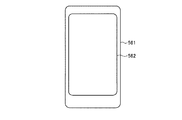
図17に示す電子機器は、表示装置10等が適用される、いわゆるスマートフォンと呼ばれる携帯電話機である。この携帯電話機は、例えば略長方形の薄板状の筐体561の表面部にタッチパネル562を有している。このタッチパネル562は、表示装置10等を備えている。
(Application example 6)
The electronic apparatus illustrated in FIG. 17 is a so-called smartphone, to which the
(適用例7)
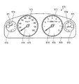
図18に示す電子機器は、車両に搭載されるメータユニットである。図18に示すメータユニット(電子機器)570は、燃料計、水温計、スピードメータ、タコメータ等、複数の液晶表示装置571を備えている。そして、複数の液晶表示装置571は、ともに、一枚の外装パネル572に覆われている。
(Application example 7)
The electronic device shown in FIG. 18 is a meter unit mounted on a vehicle. A meter unit (electronic device) 570 illustrated in FIG. 18 includes a plurality of liquid
図18に示す液晶表示装置571それぞれは、液晶表示手段としての液晶パネル573及びアナログ表示手段としてのムーブメント機構を互いに組み合わせた構成となっている。当該ムーブメント機構は、駆動手段としてのモータと、モータにより回転される指針574とを有している。そして、図18に示すように、液晶表示装置571では、液晶パネル573の表示面に目盛表示、警告表示等を表示することができるとともに、ムーブメント機構の指針574が液晶パネル573の表示面側において回転することが可能となっている。本実施の形態に係る表示装置10は液晶表示装置571に適用される。
Each of the liquid
なお、図18では、一枚の外装パネル572に複数の液晶表示装置571を設けた構成としたが、これに限定されない。外装パネルによって囲まれた領域に1つの液晶表示装置を設け、当該液晶表示装置に燃料計、水温計、スピードメータ、タコメータ等を表示させてもよい。
In FIG. 18, a plurality of liquid
以上、本発明の実施形態を説明したが、これらの実施形態の内容によりこれらの実施形態が限定されるものではない。また、前述した構成要素には、当業者が容易に想定できるもの、実質的に同一のもの、いわゆる均等の範囲のものが含まれる。さらに、前述した構成要素は適宜組み合わせることが可能である。さらに、前述した実施形態等の要旨を逸脱しない範囲で構成要素の種々の省略、置換又は変更を行うことができる。例えば、表示装置10は、有機発光ダイオード(OLED)のような自発光体を点灯する自発光型の画像表示パネルを有していてもよい。
As mentioned above, although embodiment of this invention was described, these embodiment is not limited by the content of these embodiment. In addition, the above-described constituent elements include those that can be easily assumed by those skilled in the art, those that are substantially the same, and those in a so-called equivalent range. Furthermore, the above-described components can be appropriately combined. Furthermore, various omissions, substitutions, or changes of the constituent elements can be made without departing from the spirit of the above-described embodiments and the like. For example, the
10 表示装置
20 信号処理部
21 入力部
23 信号生成部
23a α算出部
23b WG算出部
23c 伸長処理部
25 出力部
30 画像表示パネル駆動部
31 信号出力回路
32 走査回路
40 画像表示パネル
48 画素
49 副画素
49R 第1副画素
49G 第2副画素
49B 第3副画素
49W 第4副画素
50 面状光源装置制御部
60 面状光源装置
WG 第4副画素補正値
DESCRIPTION OF
Claims (10)
入力信号の入力値を、前記第1の色、前記第2の色、前記第3の色及び前記第4の色で再現される色空間の再現値に変換して生成し、生成した出力信号を前記画像表示パネルに出力する信号処理部と、を有し、
前記信号処理部は、
前記画像表示パネルに関する伸長係数を決定し、
前記第1副画素の出力信号を、少なくとも前記第1副画素の入力信号及び前記伸長係数に基づいて求めて前記第1副画素に出力し、
前記第2副画素の出力信号を、少なくとも前記第2副画素の入力信号及び前記伸長係数に基づいて求めて前記第2副画素に出力し、
前記第3副画素の出力信号を、少なくとも前記第3副画素の入力信号及び前記伸長係数に基づいて求めて前記第3副画素に出力し、
前記第4副画素の出力信号の補正値である第4副画素補正値を、前記第4副画素補正値を算出する画素の前記第1副画素の入力信号の信号値、前記第2副画素の入力信号の信号値及び前記第3副画素の入力信号の信号値のうちの最大値と、前記第4副画素補正値を算出する画素の前記第1副画素の入力信号の信号値、前記第2副画素の入力信号の信号値及び前記第3副画素の入力信号の信号値のうちの最小値と、の差が大きくなるに従って値が大きくなり、かつ、前記伸長係数が大きくなるに従って値が大きくなるように、求め、
前記第4副画素の出力信号を、前記最小値と、前記伸長係数と、前記第4副画素補正値とを乗じることにより求めて前記第4副画素に出力する表示装置。 A pixel including a first subpixel that displays a first color, a second subpixel that displays a second color, a third subpixel that displays a third color, and a fourth subpixel that displays a fourth color An image display panel having a plurality of
An output signal generated by converting an input value of an input signal into a reproduction value of a color space reproduced by the first color, the second color, the third color, and the fourth color. A signal processing unit for outputting the image to the image display panel,
The signal processing unit
Determining an expansion factor for the image display panel;
Obtaining an output signal of the first sub-pixel based on at least an input signal of the first sub-pixel and the expansion coefficient, and outputting to the first sub-pixel;
Obtaining an output signal of the second subpixel based on at least an input signal of the second subpixel and the expansion coefficient, and outputting the output signal to the second subpixel;
Obtaining an output signal of the third sub-pixel based on at least the input signal of the third sub-pixel and the expansion coefficient, and outputting to the third sub-pixel;
The fourth the fourth sub-pixel correction value is a correction value of the output signal of the sub-pixel, the signal value of the input signal of the first sub-pixel of the pixel for calculating the fourth sub-pixel correction value, the second subpixel the maximum value of the signal value and the signal value of the input signal of the third sub-pixel of the input signal, the signal value of the fourth input signal of the first sub-pixel of the pixel for calculating the sub-pixel correction value, wherein The value increases as the difference between the signal value of the input signal of the second sub-pixel and the signal value of the input signal of the third sub-pixel increases, and the value increases as the expansion coefficient increases. Asks to become larger,
A display device that obtains an output signal of the fourth subpixel by multiplying the minimum value, the expansion coefficient, and the fourth subpixel correction value, and outputs the obtained signal to the fourth subpixel.
WG=a・(Max−1/α)/Min+b The fourth subpixel correction value is WG, the expansion coefficient is α, the signal value of the input signal of the first subpixel, the signal value of the input signal of the second subpixel, and the input signal of the third subpixel. The maximum value among the signal values is Max, and the minimum is the signal value of the input signal of the first subpixel, the signal value of the input signal of the second subpixel, and the signal value of the input signal of the third subpixel. The display device according to claim 1, wherein when the value is Min and the predetermined coefficient values are a and b, the fourth subpixel correction value WG is calculated by the following equation.
WG = a · (Max−1 / α) / Min + b
WG=a・(Max−Min)+(1−1/α)+b The fourth subpixel correction value is WG, the expansion coefficient is α, the signal value of the input signal of the first subpixel, the signal value of the input signal of the second subpixel, and the input signal of the third subpixel. The maximum value among the signal values is Max, and the minimum is the signal value of the input signal of the first subpixel, the signal value of the input signal of the second subpixel, and the signal value of the input signal of the third subpixel. The display device according to claim 1, wherein when the value is Min and the predetermined coefficient values are a and b, the fourth subpixel correction value WG is calculated by the following equation.
WG = a · (Max−Min) + (1-1 / α) + b
WG=a・{(Max−Min)+(1−1/α)} The fourth subpixel correction value is WG, the expansion coefficient is α, the signal value of the input signal of the first subpixel, the signal value of the input signal of the second subpixel, and the input signal of the third subpixel. The maximum value among the signal values is Max, and the minimum is the signal value of the input signal of the first subpixel, the signal value of the input signal of the second subpixel, and the signal value of the input signal of the third subpixel. The display device according to claim 1, wherein when the value is Min and the predetermined coefficient value is a, the fourth subpixel correction value WG is calculated by the following equation.
WG = a · {(Max−Min) + (1-1 / α)}
WG=a・αC・(Max−Min)d+(1−1/α)+b The fourth subpixel correction value is WG, the expansion coefficient is α, the signal value of the input signal of the first subpixel, the signal value of the input signal of the second subpixel, and the input signal of the third subpixel. The maximum value among the signal values is Max, and the minimum is the signal value of the input signal of the first subpixel, the signal value of the input signal of the second subpixel, and the signal value of the input signal of the third subpixel. The display device according to claim 1, wherein when the value is Min and the predetermined coefficient values are a, b, c, and d, the fourth subpixel correction value WG is calculated by the following equation.
WG = a · α C · (Max−Min) d + (1-1 / α) + b
前記表示装置に前記入力信号を供給する制御装置とを有する電子機器。 A display device according to any one of claims 1 to 8,
An electronic apparatus comprising: a control device that supplies the input signal to the display device.
前記第1副画素、前記第2副画素、前記第3副画素及び前記第4副画素それぞれの出力信号を求めるステップと、
前記出力信号に基づいて、前記第1副画素、前記第2副画素、前記第3副画素及び前記第4副画素の動作を制御するステップと、を含み、
前記出力信号を求めるステップにおいては、
前記画像表示パネルに関する伸長係数を決定し、
前記第1副画素の出力信号を、少なくとも前記第1副画素の入力信号及び前記伸長係数に基づいて求め、
前記第2副画素の出力信号を、少なくとも前記第2副画素の入力信号及び前記伸長係数に基づいて求め、
前記第3副画素の出力信号を、少なくとも前記第3副画素の入力信号及び前記伸長係数に基づいて求め、
前記第4副画素の出力信号の補正値である第4副画素補正値を、前記第4副画素補正値を算出する画素の前記第1副画素の入力信号の信号値、前記第2副画素の入力信号の信号値及び前記第3副画素の入力信号の信号値のうちの最大値と、前記第4副画素補正値を算出する画素の前記第1副画素の入力信号の信号値、前記第2副画素の入力信号の信号値及び前記第3副画素の入力信号の信号値のうちの最小値と、の差が大きくなるに従って値が大きくなり、かつ、前記伸長係数が大きくなるに従って値が大きくなるように、求め、
前記第4副画素の出力信号を、前記最小値と、前記伸長係数と、前記第4副画素補正値とを乗じることにより求める表示装置の駆動方法。 A pixel including a first subpixel that displays a first color, a second subpixel that displays a second color, a third subpixel that displays a third color, and a fourth subpixel that displays a fourth color A display device having a plurality of image display panels,
Obtaining respective output signals of the first subpixel, the second subpixel, the third subpixel, and the fourth subpixel;
Controlling operations of the first subpixel, the second subpixel, the third subpixel, and the fourth subpixel based on the output signal,
In the step of obtaining the output signal,
Determining an expansion factor for the image display panel;
Obtaining an output signal of the first sub-pixel based on at least the input signal of the first sub-pixel and the expansion coefficient;
Obtaining an output signal of the second subpixel based on at least the input signal of the second subpixel and the expansion coefficient;
Obtaining an output signal of the third subpixel based on at least the input signal of the third subpixel and the expansion coefficient;
The fourth the fourth sub-pixel correction value is a correction value of the output signal of the sub-pixel, the signal value of the input signal of the first sub-pixel of the pixel for calculating the fourth sub-pixel correction value, the second subpixel the maximum value of the signal value and the signal value of the input signal of the third sub-pixel of the input signal, the signal value of the fourth input signal of the first sub-pixel of the pixel for calculating the sub-pixel correction value, wherein The value increases as the difference between the signal value of the input signal of the second sub-pixel and the signal value of the input signal of the third sub-pixel increases, and the value increases as the expansion coefficient increases. Asks to become larger,
A display device driving method for obtaining an output signal of the fourth subpixel by multiplying the minimum value, the expansion coefficient, and the fourth subpixel correction value.
Priority Applications (3)
| Application Number | Priority Date | Filing Date | Title |
|---|---|---|---|
| JP2014084041A JP6480669B2 (en) | 2014-04-15 | 2014-04-15 | Display device, display device driving method, and electronic apparatus |
| CN201510172940.3A CN105047148B (en) | 2014-04-15 | 2015-04-13 | The driving method and electronic equipment of display device, display device |
| US14/685,791 US9773470B2 (en) | 2014-04-15 | 2015-04-14 | Display device, method of driving display device, and electronic apparatus |
Applications Claiming Priority (1)
| Application Number | Priority Date | Filing Date | Title |
|---|---|---|---|
| JP2014084041A JP6480669B2 (en) | 2014-04-15 | 2014-04-15 | Display device, display device driving method, and electronic apparatus |
Publications (2)
| Publication Number | Publication Date |
|---|---|
| JP2015203808A JP2015203808A (en) | 2015-11-16 |
| JP6480669B2 true JP6480669B2 (en) | 2019-03-13 |
Family
ID=54265578
Family Applications (1)
| Application Number | Title | Priority Date | Filing Date |
|---|---|---|---|
| JP2014084041A Active JP6480669B2 (en) | 2014-04-15 | 2014-04-15 | Display device, display device driving method, and electronic apparatus |
Country Status (3)
| Country | Link |
|---|---|
| US (1) | US9773470B2 (en) |
| JP (1) | JP6480669B2 (en) |
| CN (1) | CN105047148B (en) |
Families Citing this family (5)
| Publication number | Priority date | Publication date | Assignee | Title |
|---|---|---|---|---|
| CN107331367B (en) * | 2017-08-31 | 2019-12-20 | 京东方科技集团股份有限公司 | Display device, manufacturing method thereof and method for converting color gamut standard of display device |
| KR102439146B1 (en) * | 2017-09-26 | 2022-09-02 | 삼성전자주식회사 | Display appratus and controlling method thereof |
| US11263956B2 (en) * | 2018-04-04 | 2022-03-01 | Sct Ltd. | Method and apparatus for compensating image data for LED display |
| TWI671725B (en) * | 2018-06-20 | 2019-09-11 | 友達光電股份有限公司 | Display device and method for displaying the same |
| CN109616040B (en) * | 2019-01-30 | 2022-05-17 | 厦门天马微电子有限公司 | Display device, driving method thereof and electronic equipment |
Family Cites Families (20)
| Publication number | Priority date | Publication date | Assignee | Title |
|---|---|---|---|---|
| JP2004286814A (en) * | 2003-03-19 | 2004-10-14 | Matsushita Electric Ind Co Ltd | Four-color display device |
| US7515122B2 (en) * | 2004-06-02 | 2009-04-07 | Eastman Kodak Company | Color display device with enhanced pixel pattern |
| KR100883734B1 (en) * | 2004-08-19 | 2009-02-12 | 샤프 가부시키가이샤 | Multiprimary color display device and liquid crystal display device |
| JP4073949B2 (en) * | 2005-01-26 | 2008-04-09 | シャープ株式会社 | Display device |
| KR101117980B1 (en) * | 2005-05-12 | 2012-03-06 | 엘지디스플레이 주식회사 | Apparatus and method for driving liquid crystal display device |
| TW200707374A (en) * | 2005-07-05 | 2007-02-16 | Koninkl Philips Electronics Nv | A method and apparatus of converting signals for driving a display and a display using the same |
| TWI381742B (en) * | 2005-10-13 | 2013-01-01 | Seiko Epson Corp | Image display device, electronic apparatus, and pixel location determining method |
| JP5190731B2 (en) * | 2007-10-23 | 2013-04-24 | Nltテクノロジー株式会社 | Image display device, image display method used in the image display device, and liquid crystal display device |
| JP5430068B2 (en) * | 2008-02-15 | 2014-02-26 | 株式会社ジャパンディスプレイ | Display device |
| JP5386211B2 (en) * | 2008-06-23 | 2014-01-15 | 株式会社ジャパンディスプレイ | Image display device and driving method thereof, and image display device assembly and driving method thereof |
| JP5568074B2 (en) | 2008-06-23 | 2014-08-06 | 株式会社ジャパンディスプレイ | Image display device and driving method thereof, and image display device assembly and driving method thereof |
| JP5612323B2 (en) * | 2010-01-28 | 2014-10-22 | 株式会社ジャパンディスプレイ | Driving method of image display device |
| JP5481323B2 (en) | 2010-09-01 | 2014-04-23 | 株式会社ジャパンディスプレイ | Driving method of image display device |
| JP5635463B2 (en) * | 2011-07-29 | 2014-12-03 | 株式会社ジャパンディスプレイ | Driving method of image display device |
| JP2013186294A (en) * | 2012-03-08 | 2013-09-19 | Japan Display West Co Ltd | Display device and electronic apparatus |
| JP5875423B2 (en) | 2012-03-19 | 2016-03-02 | 株式会社ジャパンディスプレイ | Image processing apparatus and image processing method |
| JP6395434B2 (en) * | 2014-05-15 | 2018-09-26 | 株式会社ジャパンディスプレイ | Display device, display device driving method, and electronic apparatus |
| JP2015227949A (en) * | 2014-05-30 | 2015-12-17 | 株式会社ジャパンディスプレイ | Display device, drive method of the display device, and electronic equipment |
| JP6359877B2 (en) * | 2014-05-30 | 2018-07-18 | 株式会社ジャパンディスプレイ | Display device, display device driving method, and electronic apparatus |
| JP6399933B2 (en) * | 2015-01-06 | 2018-10-03 | 株式会社ジャパンディスプレイ | Display device and driving method of display device |
-
2014
- 2014-04-15 JP JP2014084041A patent/JP6480669B2/en active Active
-
2015
- 2015-04-13 CN CN201510172940.3A patent/CN105047148B/en active Active
- 2015-04-14 US US14/685,791 patent/US9773470B2/en active Active
Also Published As
| Publication number | Publication date |
|---|---|
| CN105047148B (en) | 2018-06-08 |
| CN105047148A (en) | 2015-11-11 |
| US20150294642A1 (en) | 2015-10-15 |
| JP2015203808A (en) | 2015-11-16 |
| US9773470B2 (en) | 2017-09-26 |
Similar Documents
| Publication | Publication Date | Title |
|---|---|---|
| JP6423243B2 (en) | Display device, electronic apparatus, and driving method of display device | |
| JP6154305B2 (en) | Display device and electronic device | |
| JP2014139647A (en) | Display device, driving method of display device, and electronic apparatus | |
| JP6480669B2 (en) | Display device, display device driving method, and electronic apparatus | |
| JP2015230343A (en) | Display device | |
| JP2015219372A (en) | Display device | |
| JP6637396B2 (en) | Display device, electronic device, and method of driving display device | |
| US9972255B2 (en) | Display device, method for driving the same, and electronic apparatus | |
| JP2015210388A (en) | Display device | |
| JP6395434B2 (en) | Display device, display device driving method, and electronic apparatus | |
| JP2016061858A (en) | Image display panel, image display device, and electronic apparatus | |
| US10127885B2 (en) | Display device, method for driving the same, and electronic apparatus | |
| US20140125689A1 (en) | Display device, electronic apparatus, and drive method for display device | |
| JP6479337B2 (en) | Display device, method of driving display device, and electronic apparatus | |
| JP2016114789A (en) | Display device and color conversion method | |
| US9734772B2 (en) | Display device | |
| JP6042785B2 (en) | Display device, electronic apparatus, and driving method of display device | |
| KR20130143509A (en) | Signal processing circuit, display device and electronic apparatus | |
| US20150356933A1 (en) | Display device | |
| JP6389714B2 (en) | Image display device, electronic apparatus, and driving method of image display device | |
| JP2015082021A (en) | Display device, driving method of display device, and electronic apparatus | |
| KR20220048943A (en) | IR-drop compensation for a display panel including areas of different pixel layouts | |
| JP6399933B2 (en) | Display device and driving method of display device | |
| JP2015219362A (en) | Display device, method for driving display device, and electronic apparatus | |
| JP2015210445A (en) | Display device, electronic apparatus, method for driving display device and signal processing circuit |
Legal Events
| Date | Code | Title | Description |
|---|---|---|---|
| A621 | Written request for application examination |
Free format text: JAPANESE INTERMEDIATE CODE: A621 Effective date: 20161209 |
|
| A977 | Report on retrieval |
Free format text: JAPANESE INTERMEDIATE CODE: A971007 Effective date: 20170920 |
|
| A131 | Notification of reasons for refusal |
Free format text: JAPANESE INTERMEDIATE CODE: A131 Effective date: 20171107 |
|
| A521 | Request for written amendment filed |
Free format text: JAPANESE INTERMEDIATE CODE: A523 Effective date: 20171225 |
|
| A131 | Notification of reasons for refusal |
Free format text: JAPANESE INTERMEDIATE CODE: A131 Effective date: 20180605 |
|
| A521 | Request for written amendment filed |
Free format text: JAPANESE INTERMEDIATE CODE: A523 Effective date: 20180802 |
|
| TRDD | Decision of grant or rejection written | ||
| A01 | Written decision to grant a patent or to grant a registration (utility model) |
Free format text: JAPANESE INTERMEDIATE CODE: A01 Effective date: 20190122 |
|
| A61 | First payment of annual fees (during grant procedure) |
Free format text: JAPANESE INTERMEDIATE CODE: A61 Effective date: 20190208 |
|
| R150 | Certificate of patent or registration of utility model |
Ref document number: 6480669 Country of ref document: JP Free format text: JAPANESE INTERMEDIATE CODE: R150 |
|
| R250 | Receipt of annual fees |
Free format text: JAPANESE INTERMEDIATE CODE: R250 |
|
| R250 | Receipt of annual fees |
Free format text: JAPANESE INTERMEDIATE CODE: R250 |
|
| R250 | Receipt of annual fees |
Free format text: JAPANESE INTERMEDIATE CODE: R250 |