EP1538560B1 - Antenna for radio frequency identification - Google Patents
Antenna for radio frequency identification Download PDFInfo
- Publication number
- EP1538560B1 EP1538560B1 EP04026191A EP04026191A EP1538560B1 EP 1538560 B1 EP1538560 B1 EP 1538560B1 EP 04026191 A EP04026191 A EP 04026191A EP 04026191 A EP04026191 A EP 04026191A EP 1538560 B1 EP1538560 B1 EP 1538560B1
- Authority
- EP
- European Patent Office
- Prior art keywords
- antenna
- slit
- rfid
- base film
- length
- Prior art date
- Legal status (The legal status is an assumption and is not a legal conclusion. Google has not performed a legal analysis and makes no representation as to the accuracy of the status listed.)
- Expired - Fee Related
Links
Images


Classifications
-
- H—ELECTRICITY
- H01—ELECTRIC ELEMENTS
- H01Q—ANTENNAS, i.e. RADIO AERIALS
- H01Q1/00—Details of, or arrangements associated with, antennas
- H01Q1/36—Structural form of radiating elements, e.g. cone, spiral, umbrella; Particular materials used therewith
- H01Q1/38—Structural form of radiating elements, e.g. cone, spiral, umbrella; Particular materials used therewith formed by a conductive layer on an insulating support
-
- G—PHYSICS
- G06—COMPUTING; CALCULATING OR COUNTING
- G06K—GRAPHICAL DATA READING; PRESENTATION OF DATA; RECORD CARRIERS; HANDLING RECORD CARRIERS
- G06K19/00—Record carriers for use with machines and with at least a part designed to carry digital markings
- G06K19/06—Record carriers for use with machines and with at least a part designed to carry digital markings characterised by the kind of the digital marking, e.g. shape, nature, code
- G06K19/067—Record carriers with conductive marks, printed circuits or semiconductor circuit elements, e.g. credit or identity cards also with resonating or responding marks without active components
- G06K19/07—Record carriers with conductive marks, printed circuits or semiconductor circuit elements, e.g. credit or identity cards also with resonating or responding marks without active components with integrated circuit chips
- G06K19/077—Constructional details, e.g. mounting of circuits in the carrier
- G06K19/07749—Constructional details, e.g. mounting of circuits in the carrier the record carrier being capable of non-contact communication, e.g. constructional details of the antenna of a non-contact smart card
- G06K19/07773—Antenna details
- G06K19/07777—Antenna details the antenna being of the inductive type
- G06K19/07779—Antenna details the antenna being of the inductive type the inductive antenna being a coil
- G06K19/07783—Antenna details the antenna being of the inductive type the inductive antenna being a coil the coil being planar
-
- G—PHYSICS
- G06—COMPUTING; CALCULATING OR COUNTING
- G06K—GRAPHICAL DATA READING; PRESENTATION OF DATA; RECORD CARRIERS; HANDLING RECORD CARRIERS
- G06K19/00—Record carriers for use with machines and with at least a part designed to carry digital markings
- G06K19/06—Record carriers for use with machines and with at least a part designed to carry digital markings characterised by the kind of the digital marking, e.g. shape, nature, code
- G06K19/067—Record carriers with conductive marks, printed circuits or semiconductor circuit elements, e.g. credit or identity cards also with resonating or responding marks without active components
- G06K19/07—Record carriers with conductive marks, printed circuits or semiconductor circuit elements, e.g. credit or identity cards also with resonating or responding marks without active components with integrated circuit chips
- G06K19/077—Constructional details, e.g. mounting of circuits in the carrier
- G06K19/07749—Constructional details, e.g. mounting of circuits in the carrier the record carrier being capable of non-contact communication, e.g. constructional details of the antenna of a non-contact smart card
- G06K19/07773—Antenna details
- G06K19/07786—Antenna details the antenna being of the HF type, such as a dipole
-
- H—ELECTRICITY
- H01—ELECTRIC ELEMENTS
- H01Q—ANTENNAS, i.e. RADIO AERIALS
- H01Q1/00—Details of, or arrangements associated with, antennas
- H01Q1/12—Supports; Mounting means
- H01Q1/22—Supports; Mounting means by structural association with other equipment or articles
-
- H—ELECTRICITY
- H01—ELECTRIC ELEMENTS
- H01Q—ANTENNAS, i.e. RADIO AERIALS
- H01Q23/00—Antennas with active circuits or circuit elements integrated within them or attached to them
-
- H—ELECTRICITY
- H01—ELECTRIC ELEMENTS
- H01Q—ANTENNAS, i.e. RADIO AERIALS
- H01Q7/00—Loop antennas with a substantially uniform current distribution around the loop and having a directional radiation pattern in a plane perpendicular to the plane of the loop
-
- H—ELECTRICITY
- H01—ELECTRIC ELEMENTS
- H01L—SEMICONDUCTOR DEVICES NOT COVERED BY CLASS H10
- H01L2224/00—Indexing scheme for arrangements for connecting or disconnecting semiconductor or solid-state bodies and methods related thereto as covered by H01L24/00
- H01L2224/01—Means for bonding being attached to, or being formed on, the surface to be connected, e.g. chip-to-package, die-attach, "first-level" interconnects; Manufacturing methods related thereto
- H01L2224/10—Bump connectors; Manufacturing methods related thereto
- H01L2224/15—Structure, shape, material or disposition of the bump connectors after the connecting process
- H01L2224/16—Structure, shape, material or disposition of the bump connectors after the connecting process of an individual bump connector
-
- H—ELECTRICITY
- H01—ELECTRIC ELEMENTS
- H01L—SEMICONDUCTOR DEVICES NOT COVERED BY CLASS H10
- H01L2924/00—Indexing scheme for arrangements or methods for connecting or disconnecting semiconductor or solid-state bodies as covered by H01L24/00
- H01L2924/10—Details of semiconductor or other solid state devices to be connected
- H01L2924/11—Device type
- H01L2924/13—Discrete devices, e.g. 3 terminal devices
- H01L2924/1304—Transistor
- H01L2924/1306—Field-effect transistor [FET]
- H01L2924/13091—Metal-Oxide-Semiconductor Field-Effect Transistor [MOSFET]
-
- H—ELECTRICITY
- H01—ELECTRIC ELEMENTS
- H01L—SEMICONDUCTOR DEVICES NOT COVERED BY CLASS H10
- H01L2924/00—Indexing scheme for arrangements or methods for connecting or disconnecting semiconductor or solid-state bodies as covered by H01L24/00
- H01L2924/30—Technical effects
- H01L2924/301—Electrical effects
- H01L2924/3011—Impedance
Description
- This invention relates to an antenna for radio frequency identification that performs wireless identification, in particular, miniaturization thereof.
- Conventionally, a technology has been proposed with which impedance matching of an antenna for radio frequency identification (RFID) is established using an antenna pattern existing parallel to a main antenna. Generally, the highest efficiency is attained with an antenna having a length that is half of the wavelength of the frequency (λ/2) used and there is also a case where a λ/4 grounded antenna is used for the sake of miniaturization of a device (refer to US 6100804 B).
- In the conventional technique described above, however, an antenna is constructed of plural separated antenna patterns, thereby being difficult to realize a compact antenna using such a construction.
- RFID is attached to merchandise or a product so that merchandise control, product quality control, or the like is performed by utilizing the ID number or the like possessed by the RFID. Under the Radio Law in Japan, the main frequency bands that the RFID can use are 2.45 GHz, 13.56 MHz, and 125 kHz. Even when 2.45 GHz is used, its half-wavelength is approximately 6 cm. Thus, when importance is placed on the efficiency of an antenna, the size of the antenna becomes as large as approximately 6 cm.
- Here, the size (length, width) of the RFID is determined by the size of the antenna, which results in a situation where the size of the RFID exceeds the size of merchandise or a product to which the RFID is to be attached, assuming that the merchandise or product is a small object such as a medicine bottle. Such a situation where the size of the RFID exceeds the size of the merchandise or product, to which the RFID is to be attached, is not preferable because there occur various problems in that the RFID is peeled off during production, distribution, transportation, or the like of the merchandise or product.
- US 2003/063002 A1 discloses an antenna with the features of the pre-characterising portion of appended
claims 1 and 3. - EP 1 0055 943 a2 describes a microstrip patch designed as a resonant antenna.
- It is desired to devise an antenna that can be unified and compact. It is therefore an object of this invention to reduce the size of an antenna, thereby achieving a reduction in size of the RFID itself using the antenna, and providing the RFID or the like that does not exceed the size of an object to which the RFID or the like is to be attached.
- The object is met by the antennas defined in
claims 1 and 3. The dependent claims relate to preferred modifications of the invention. - According to the embodiment of this invention, it is possible to produce an integrated and compact antenna.
- The present invention can be appreciated by the description which follows in conjunction with the following figures, wherein:
- FIG. 1A is a plane view of RFID using an antenna according to a first embodiment of this invention.
- FIG. 1B is a cross-sectional view of the RFID taken along the line A-A' shown in FIG. 1A.
- FIG. 2 is a block diagram showing a construction of the RFID according to the embodiment of this invention.
- FIG. 3 is a block diagram showing the principle of operation of the antenna for the RFID according to the embodiment of this invention.
- FIG. 4 is a characteristic diagram of the antenna for the RFID according to the embodiment of this invention.
- FIG. 5 is another characteristic diagram of the antenna for the RFID according to the embodiment of this invention.
- FIG. 6A is a plane view of RFID using an antenna according to a second embodiment of this invention.
- FIG. 6B is a cross-sectional view of the RFID taken along the line A-A' shown in FIG. 6A.
- FIG. 7A is a plane view of RFID using an antenna according to a modification of the second embodiment of this invention.
- FIG. 7B is a cross-sectional view of the RFID taken along the line A-A' shown in FIG. 7A.
- FIG. 8A is a plane view of RFID using an antenna according to a third embodiment of this invention.
- FIG. 8B is a cross-sectional view of the RFID taken along the line A-A' shown in FIG. 8A.
- FIG. 9 is a perspective view of RFID using an antenna according to a fourth embodiment of this invention.
- FIG. 10A is a plane view of RFID using an antenna according to a fifth embodiment of this invention.
- FIG. 10B is a cross-sectional view of the RFID taken along the line A-A' shown in FIG. 10A.
- FIG. 11 is an explanatory diagram of a method of producing the RFID using the antenna according to the fifth embodiment of this invention.
- FIG. 12 is a plane view of RFID using an antenna according to a sixth embodiment of this invention.
- FIG. 13A is a plane view of RFID using an antenna according to a seventh embodiment of this invention.
- FIG. 13B is a cross-sectional view of the RFID taken along the line A-A' shown in FIG. 13A.
- FIG. 14A is a plane view of RFID using an antenna according to an eighth embodiment of this invention.
- FIG. 14B is an A-A' cross-sectional view of the RFID shown in FIG. 14A.
- FIG. 15 is a perspective view of an embodiment where the RFID according to the embodiments of this invention is affixed to a receiving container.
- When the size of an antenna is set smaller than the half-wavelength of the frequency used, due to the properties thereof, it is impossible to obtain a resonant condition so that efficient transmission and reception cannot be performed using effectively the maximum electric power. Also, it is required to pass electric power with efficiency at a connection from a high-frequency output circuit to an antenna and to prevent a radio wave reflection problem from occurring. Therefore, in an embodiment of this invention, a demerit resulting from a situation where no resonance is obtained due to a reduction in size of an antenna to less than a half-wavelength is compensated for by matching the impedance of the circuit (which is typically a semiconductor integrated circuit) of RFID to that of the antenna.
- The embodiments of this invention will now be described with reference to the accompanying drawings.
- FIG. 1A is a plane view of RFID using an antenna according to a first embodiment of this invention and FIG. 1B is a cross-sectional view taken along the line A-A' of FIG. 1A.
- An
antenna 101 is formed on abase film 106 using a conductive pattern and an opening (in the following also referred to as slit) 102 is established in theantenna 101. AnRFID chip 103 is provided with afirst bump 104 and asecond bump 105 and theRFID chip 103 and theantenna 101 are connected to each other through thebumps bumps 104 and 105 (input impedance of the RFID chip 103) is adjusted to 60 Ω at 2.45 GHz, for instance. It should be noted that a construction may also be used in which the length of the antenna is shortened by using a high-dielectric-constant base material as thebase film 106. - In the embodiment of this invention, by providing the
antenna 101 with theslit 102, impedance matching between theantenna 101 and theRFID chip 103 is established. - When a microwave of 2.45 GHz is irradiated to the
antenna 101, a high-frequency current is caused to flow through theantenna 101. Under this state, when matching is established between the input impedance (60 Ω) of theRFID chip 103 and the impedance of the antenna, the high-frequency current flowing through theantenna 101 can be supplied to theRFID chip 103 with the highest efficiency. On the other hand, when the matching between the input impedance of theRFID chip 103 and the impedance of the antenna is incomplete, as the high-frequency current is reflected at the connection points (bumps 104 and 105) therebetween, sufficient energy cannot be supplied to theRFID chip 103 to operate. As a result, the strength of a signal inputted into theRFID chip 103 is weakened. - FIG. 2 is a block diagram showing a construction of the RFID according to the embodiment of this invention.
- The
RFID chip 103 includes arectifier circuit 302, aclock extracting circuit 303, aload switch 304, and a counter/memory circuit 305. - The
antenna 101 is connected to therectifier circuit 302. The high-frequency current flowing through theantenna 101 is rectified by therectifier circuit 302 and then is inputted into theclock extracting circuit 303. In theclock extracting circuit 303, a clock width and a clock interval are extracted from a high-frequency carrier with precision. An extracted low-frequency clock pulse is inputted into the counter/memory circuit 305, which then performs processing such as certification of the RFID. - An output from the counter/
memory circuit 305 is inputted into theload switch 304. Theload switch 304 is a switching device composed of MOSFETs and performs load modulation by changing impedance with respect to the antenna 101 (impedance between thebumps 104 and 105). A modulated signal is transmitted from theantenna 101 to a reader for the RFID as data. - The input impedance of the
rectifier circuit 302 is determined by the value of its internal load, in other words, the scheme adopted by therectifier circuit 302, the shape of rectifiers, the parasitic effect of the rectifier circuit, and the like. In the high-frequency rectifier circuit 302, its parasitic capacitance is a significant impedance factor. Therefore, when the matching between theantenna 101 and therectifier circuit 302 is insufficient, the energy from theantenna 101 is not sufficiently supplied to therectifier circuit 302. In order to establish matching at a high frequency, an antenna line is required to be dealt with as a distributed constant circuit. It is also required that theantenna 101 functions not only as a resonant circuit but also as a matching circuit for the high-frequency current to the RFID chip. In this case, the matching means a situation where the high-frequency current is inputted from theantenna 101 to theRFID chip 103 without being reflected in a transition portion to a different system (connection points between theantenna 101 and the RFID chip 103). - Therefore, it is required to provide the antenna with a matching circuit. In the embodiment of this invention, the
slit 102 is formed in a terminal portion (between thebumps 104 and 105) of theRFID chip 103. In other words, it is required that theRFID chip 103 is provided at an end portion of theslit 102. This slit 102 is at the same voltage in terms of a direct current. A current, however, flows in an alternating manner, so a shape of theslit 102 is important. Theslit 102 forms a current distributed constant circuit with respect to the input terminals (bumps 104 and 105) of theRFID chip 103. - FIG. 3 is a block diagram showing the principle of operation of the antenna for the RFID according to the embodiment of this invention and shows the equivalent circuit of the
slit 102 when theantenna 101 is connected to theRFID chip 103. - The
slit 102 constitutes the distributed constant circuit, an inductance L exists along a slit length, and a capacitance C exists inversely proportional to a slit width. The characteristic impedance of the distributed constant circuit is expressed by a square root found by dividing the inductance L by the capacitance C. Consequently, the slit length is in an approximately proportional relation with the inductance L and when the slit length is lengthen, the inductance L is increased. The slit width is in an approximately inversely proportional relation with the capacitance C and when the slit width is widened, the capacitance C is decreased. - When matching is established by setting the terminals of the distributed constant circuit so as to have the same impedance, energy can be transmitted without reflection. When the slit width is increased, the capacitance C is decreased. Accordingly, in order to maintain the characteristic impedance at the same level, it is required to decrease the inductance L by electrically shortening the slit length.
- Even when the input impedance of the RFID chip is changed, impedance matching can be established by freely adjusting matching based on the slit length and the slit width in the manner described above. Also, when the slit length is short, a compact antenna can be easily realized. Further, with the large slit width, production accuracy is not need to be very high (aluminum punching becomes usable, for instance), thereby making it possible to produce an antenna at a low price.
- FIG. 4 is a characteristic diagram of the antenna for the RFID according to the embodiment of this invention and shows results of an experiment where a communication distance between the antenna of the reader and the RFID is measured while changing the slit length and the slit width of the antenna shown in FIG. 1.
- In FIG. 4, results obtained by setting the slit length to 3 mm, 4 mm, and 5 mm are shown in the diagram. It can be understood from this diagram that as the slit length is shortened, the slit width, with which the maximum communication distance is obtained, is increased and the range of the slit width where the maximum communication distance (250 mm) is obtained with stability is widened. Also, as described with FIG. 3, when the slit width is widened to reduce the capacitance C, it is required to reduce inductance L in order to maintain the characteristic impedance at the same level. In other words, it is required to electromagnetically shorten the slit length, which matches with the measurement data in FIG. 4. In FIG. 4, the maximum communication distance is saturated at 250 mm, which is not due to the antenna shape, but due to factors, such as an output from the reader, and the like.
- In this invention, adjustment of the size (length and width) of the slit in order to establish impedance matching makes it possible to construct a compact antenna. In other words, unlike in the conventional case, it is not required to use a pattern separated from an antenna element, so an antenna can be constructed as being integrated, rectangular, and compact. Further, by increasing the slit width, the slit length can be shortened miniaturize the antenna. This means that it is possible to shorten the whole of the antenna, and important conditions for constructing a compact antenna with this invention have been determined. It can be understood from FIG. 4 that the communication distance is stabilized with the slit width of 0.4 mm or more.
- FIG. 5 is another characteristic diagram of the antenna for the RFID according to the embodiment of this invention and shows the measurement data shown in FIG. 4 as a relation between the slit width and the slit length.
- FIG. 5 shows a region where a communication distance of 200 mm is obtained and a region where the maximum communication distance (250 mm) is obtained.
- It can be understood from FIG. 5 that it is possible to increase the slit width by shortening the slit length. In addition, it also can be understood that when the slit length is shortened, the allowable range of the slit width is widened. This is conceivably because a strict distributed constant circuit becomes a mixed model of a distributed constant circuit and a concentrated constant circuit, as the slit width is required to be widened with the slit length shortened.
- More specifically, when the slit length is 5 mm, it is required to construct the antenna under a severe condition where the slit width is 0.4 mm while the size the antenna being set so as to have a length that is equal to or more than the slit length (5 mm). On the other hand, when the slit length is 3 mm, it is possible to obtain the maximum communication distance with the slit width between 1.0 mm and 1.4 mm. As a result, it is possible to produce a compact antenna with alleviated production accuracy, using economical specifications, and at low cost.
- As shown in FIG. 6A to FIG. 8B, the area of the antenna is the sum total of the area of a conductor forming the antenna and the area of the slit. By setting a slit size with the slit length being 2.4 mm through 3.0 mm, the slit width being 1.0 mm through 1.4 mm, and the slit area being 3.0 mm through 4.2 mm, a compact antenna can be produced with maximum size (length or width) being 3.0 mm or less, while obtaining the maximum communication distance or a communication distance close to maximum.
- Also, as shown in FIG. 5 to FIG. 12, the maximum size (length or width) of the antenna according to the embodiment of this invention is defined by the slit length and slit width thereof and is determined by the size of greater one of the slit length and the slit width.
- In other words, when the slit length is greater than the slit width (slit length > slit width), the antenna length is greater than the antenna width (antenna length > antenna width) and the maximum size of the antenna is determined by the antenna length. In this case, for instance, the maximum size of the antenna is the sum total of the width of the conductor forming the antenna and the slit length. On the other hand, when the slit length is smaller than the slit width (slit length < slit width), the antenna length is smaller than the antenna width (antenna length < antenna width) and the maximum size of the antenna is determined by the antenna width.
- Accordingly, the maximum size of the antenna is to be the minimum at a point where the antenna length and the antenna width are equal to each other (antenna length = antenna width). In this case, for instance, the maximum size of the antenna is the sum total of the width of the conductor forming the antenna and the slit width. In other words, the maximum size of the antenna becomes the minimum when the slit length and the slit width are set equal to each other. In FIG. 13, an example of an antenna constructed in this manner is shown. Also, in FIG. 5, illustrated is a straight line expressing points where the slit length and the slit width are equal to each other.
- Consequently, when the slit is formed so as to have a slit size on the straight line expressing the points where the slit length and the slit width are equal to each other in the region shown in FIG. 5 where the maximum communication distance is obtained, or in other words, when the slit is formed so that the slit length and the slit width are equal to each other and is 2.0 mm through 2.4 mm, the maximum size of the antenna becomes the minimum while the maximum communication distance being obtained.
- As can be understood from FIG. 5, by constructing the antenna in the shape according to the first embodiment of this invention, it is possible to produce a RFID chip where the antenna is miniaturized and a practical communication distance is secured while managing a reduction in communication distance due to the miniaturization. In addition, miniaturization of the antenna also makes it possible to miniaturize the RFID provided with the antenna, which widens the range of objects to which the RFID can be attached. For instance, the RFID can be attached to the lid portion of a small medicine bottle or the like.
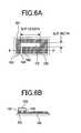
- FIG. 6A is a plane view of RFID using an antenna according to a second embodiment of this invention and FIG. 6B is a cross-sectional view taken along the line A-A' of FIG. 6A.
- The antenna according to the second embodiment is a shortened antenna where the edge of the antenna is set close to the slit by narrowing the outer width of the antenna 501 (by setting the width of the conductor forming the antenna to 1 mm or less, for instance). It should be noted that each construction element that functions in the same manner as in the first embodiment described above is given the same reference numeral and the detailed description thereof will be omitted.
- In the second embodiment, an
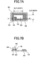
antenna 501 is formed by a conductive pattern on abase film 106 and aslit 102 is established in theantenna 501. Also, theantenna 501 is connected to afirst bump 104 and asecond bump 105 provided for anRFID chip 103. - FIG. 7A is a plane view of RFID using an antenna as a modification according to the second embodiment of this invention and FIG. 7B is a cross-sectional view taken along the line A-A' of FIG. 7A.
- In the modification according to the second embodiment, like in the first embodiment shown in FIG. 6, an
antenna 601 is formed by a conductive pattern on abase film 106 and aslit 602 is established in theantenna 601. Also, theantenna 601 is connected to afirst bump 104 and asecond bump 105 provided for anRFID chip 103. - As described above, in the second embodiment, by narrowing the width of the electric conductor forming the outer portion of the antenna, the slit length can be shortened to make it further possible to miniaturize the antenna. Also, in the modification shown in FIG. 7, with the
slit width 602 partially enlarged, it is possible to further shorten the slit length to miniaturize the antenna. - FIG. 8A is a plane view of RFID using an antenna according to a third embodiment of this invention and FIG. 8B is a cross-sectional view taken along the line A-A' of FIG. 8A.
- The antenna according to the third embodiment is characterized in that a high-dielectric-
constant cover sheet 702 is provided for the upper surface of theantenna 601. It should be noted that each construction element that functions in the same manner as in the first or second embodiment described above is given the same reference numeral and the detailed description thereof will be omitted. - In the third embodiment, an
antenna 601 is formed by a conductive pattern on a high-dielectric-constant base film 701 and aslit 602 is established in theantenna 601. Also, theantenna 601 is connected to afirst bump 104 and asecond bump 105 provided for anRFID chip 103. - As described above, in the third embodiment, the high-dielectric-
constant cover sheet 702 is provided so as to cover the upper surface of theantenna 601 and theantenna 601 is sandwiched between the high-dielectric-constant base film 701 and the high-dielectric-constant cover sheet 702. With this construction, a wavelength shortening effect is produced, which makes it possible to miniaturize the antenna without shortening the communication distance. - FIG. 9 is a perspective view of RFID using an antenna according to a fourth embodiment of this invention.
- The RFID according to the fourth embodiment is characterized in that a
RFID chip 804 with electrodes provided on both surfaces thereof is used. It should be noted that each construction element that functions in the same manner as in the first through third embodiments described above is given the same reference numeral and the detailed description thereof will be omitted. - An
antenna 801 constituted of an electric conductor (conductive pattern provided on a base film, for instance) is provided with aslit 802 and a foldedportion 803 extending from the antenna conductor is folded to a position overlapping theantenna 801. Also, theRFID chip 804 with electrodes provided on both surfaces thereof is arranged under the foldedportion 803. In other words, one end of theantenna 801 is connected to one of the electrodes provided on the both surfaces of theRFID chip 804 and one end of the foldedportion 803 is connected to the other of the electrodes of theRFID chip 804. - Even with the structure according to the fourth embodiment, illustrated in FIG. 4 is the relation between the slit length and the slit width. In order to construct an antenna having a short antenna length, it is important to shorten the slit length and to widen the slit width.
- As described above, in the fourth embodiment, a sandwich structure is adopted in which the
antenna 801 is folded and is connected to the electrodes provided on the both surfaces of theRFID chip 804, so it becomes possible to produce a more compact antenna. - FIG. 10A is a plane view of RFID using an antenna according to a fifth embodiment of this invention and FIG. 10B is a cross-sectional view taken along the line A-A' of FIG. 10A.
- The antenna for the RFID according to the fifth embodiment is characterized in that a slit is provided in a slanting direction. It should be noted that each construction element that functions in the same manner as in the first through fourth embodiments described above is given the same reference numeral and the detailed description thereof will be omitted.
- An
antenna 910 through 911 provided on abase film 906 has aslit 802. Theslit 802 constitutes aseparation groove 908 by extending in a slanting direction and separates the antenna into twoend portions end portion 910 of the antenna is connected to one of electrodes provided on the both surfaces of anRFID chip 804. Also, theend portion 911 of the antenna is connected to acover metal 903 provided for acover film 904. - The
conductive cover metal 903 is provided on a lower surface of thecover film 904. A layer of anisotropicconductive adhesives 905 is provided between thebase film 906 and the cover film 904 (between theantenna 910 through 911 and the cover metal 903). The anisotropicconductive adhesives 905 do not have conductivity under an ordinary state but exhibits conductivity through application of a pressure in a direction in which the pressure is applied. Consequently, by applying a pressure at ashort point 909 provided on anantenna 911 side on the base film 906 (applying a pressure from acover film 904 side as shown in FIG. 10, for instance), electrical continuity is established between theantenna 911 of thebase film 906 and thecover metal 903 of thecover film 904. - One of the electrodes of the
RFID chip 804 is connected to theend portion 910 of the antenna. Also, the other of the electrodes of theRFID chip 804 is connected to thecover metal 903 of thecover film 904. - Even with the structure according to the fourth embodiment, illustrated in FIG. 4 is the relation between the slit length and the slit width. In order to construct an antenna having a short antenna length, it is important to shorten slit length and to widen the slit width.
- Next, by referring to FIG. 11, a method of producing the RFID shown in FIGS. 10A and 10B will be described.
- First,
plural RFID chips 804 are mounted at predetermined positions on thebase film 906 where plural antennas are continuously provided, and then the anisotropicconductive adhesives 905 are arranged. Following this, thecover film 904 whereplural cover metals 903 are continuously provided is overlaid on thebase film 906 and theshort points 909 are pressurized from thecover film 904 side. Finally, thebase film 906 and thecover film 904 are cut along the lines C. In this manner, the RFID shown in FIGS. 10A and 10B is produced. - As described above, in the fifth embodiment, providing the slit in a slanting direction makes it possible to increase the tolerance to displacements of the arrangement position of the
RFID chip 804 and the position of theshort point 909. As a result, the RFID can be supplied at a low price. - FIG. 12 is a plane view of RFID using an antenna according to a sixth embodiment of this invention.
- The antenna for the RFID according to the sixth embodiment is characterized in that the corner portions of the antenna according to the modification shown in FIG. 7 of the second embodiment are removed. It should be noted that each construction element that functions in the same manner as in the first through fifth embodiments described above is given the same reference numeral and the detailed description thereof will be omitted.
- In this sixth embodiment, like in the modification shown in FIG. 7 of the second embodiment, an
antenna 601 is formed by a conductive pattern on abase film 106 and aslit 602 is established in theantenna 601. In the sixth embodiment, even thecorner portions 1001 of theantenna 601 are removed, a high-frequency current mainly flows in the vicinity of the center portion of theantenna 601 and does not flow in the corner portions of theantenna 601. Therefore, even the corner portions of theantenna 601 are removed, no influences are exerted on the performance of the antenna. Also, theantenna 601 is connected to afirst bump 104 and asecond bump 105 provided for anRFID chip 103. - Even with the structure according to the sixth embodiment, illustrated in FIG. 4 is the relation between the slit length and the slit width. In order to construct an antenna having a short antenna length, it is important to shorten the slit length and widen the slit width.
- As described above, in the sixth embodiment, removing the corner portions of the antenna without exerting any influences on the performance of the antenna makes it possible to miniaturize the antenna so as to realize RFID that can be attached in a narrow and small space.
- FIG. 13A is a plane view of RFID using an antenna according to a seventh embodiment of this invention and FIG. 13B is a cross-sectional view taken along the line A-A' of FIG. 13A.
- The antenna for the RFID according to the seventh embodiment is characterized in that it has a quadrangular shaped. It should be noted that each construction element that functions in the same manner as in the first through sixth embodiments described above is given the same reference numeral and the detailed description thereof will be omitted.
- In the seventh embodiment, an
antenna 1201 having a quadrangular shape is formed by a conductive pattern on abase film 1202 having a quadrangular shape and a slit having a quadrangular shape is established in theantenna 1201. In other words, a shape is used in which the length of the slit and the width of the slit are set equal to each other or approximately equal to each other. Also, theantenna 1201 is connected to afirst bump 104 and asecond bump 105 provided for anRFID chip 103. - FIG. 14A is a plane view of RFID using an antenna according to a eighth embodiment of this invention and FIG. 14B is a cross-sectional view taken along the line A-A' of FIG. 14A.
- The antenna for the RFID according to the eighth embodiment is characterized in that it has a circular shape. It should be noted that each construction element that functions in the same manner as in the first through seventh embodiments described above is given the same reference numeral and the detailed description thereof will be omitted.
- In the eighth embodiment, an
antenna 1301 having a circular shape is formed by a conductive pattern on abase film 1302 having a circular shape and a slit having a circular shape is established in theantenna 1301. In other words, a shape is used in which the length of the slit and the width of the slit are set equal to each other or approximately equal to each other. Also, theantenna 1301 is connected to afirst bump 104 and asecond bump 105 provided for anRFID chip 103. - Even with the structures according to the seventh and eighth embodiments, illustrated in FIG. 4 is the relation between the slit length and the slit width. In the seventh embodiment, the slit length and the slit width are set approximately equal to each other. In other words, in this invention, the shortening of the slit length is approximately equal to the widening of the slit width and the seventh embodiment is based on the essence of this invention. It should be noted that the circuit with the circular-shaped slit as in the eighth embodiment can be the equivalent circuit same as that with the quadrangular-shaped slit.
- As described above, in the seventh and eighth embodiments, setting the slit length and the slit width approximately equal to each other makes it possible to miniaturize the antenna without exerting any influences on the performance of the antenna so as to realize RFID that can be attached in a narrow and small space.
- FIG. 15 is a perspective view of an embodiment where the RFID according to the embodiments of this invention is affixed to a receiving container (e.g. bottle).
- An RFID chip provided with the compact antenna according to this invention is attached to a
lid portion 1103 of the container. Containers (bottles) made of glass, plastic, or another material are used in various fields in order to store or keep various medicines or samples, although there is a case where the mixing of foreign matters into the contents, the chemical reaction of the contents, or the like occurs during production or keeping. Therefore, it is required to periodically check the contents during the production or keeping. In order to automatically register results of the check in a computer, it is desirable that the container can be automatically identified. Conventionally, for the sake of the automatic identification, a barcode, an IC chip for wireless identification, or the like were attached to such a container. In this case, however, when the container is small, no space for affixation of a label for identification is found on the top surface or the bottom surface of the container and the label is affixed to the periphery of the container, which leads to a problem that the label interferes with the observation of the contents. With the RFID chip using the compact antenna according to this invention is attached to the lid of the bottle no matter to which position amain body 1104 of the bottle is rotated, it is possible to read the chip with ease. - The antenna according to this invention can be applied to an RFID chip. As the antenna can be miniaturized, it is suitable to be provided for the RFID that should be compact for application to the merchandise management at stores, the identification of medicines or samples, tickets for transportation or entertainment, or the like.
- While the present invention has been described in detail and pictorially in the accompanying drawings, the present invention is not limited to such detail but covers various obvious modifications and equivalent arrangements, which fall within the purview of the appended claims.
Claims (12)
- A non-resonant antenna designed to operate at substantially 2.45 GHz and connected to an IC chip (103) for wireless identification, the antenna (101 ,501, 601 801, 910) comprising a conductor having an opening (102) and two connection points (104, 105) separated by the opening (102), characterised in that
the length of the opening (102) is in the range of 2.4 mm to 3.0 mm,
the width of the opening (102) is in the range of 1.0 mm to 1.4 mm, and
the area of the opening (102) is in the range of 3.0 mm2 to 4.2 mm2. - The antenna of claim 1, wherein the length of the opening (102) is substantially 3 mm.
- A non-resonant antenna designed to operate at substantially 2.45 GHz and connected to an IC chip (103) for wireless identification, wherein the antenna (1201, 1301) comprises a conductor having an opening (102) and two connection points (104, 105) separated by the opening (102),
characterised in that the length and the width of the opening (102) are substantially equal and are both in the range of 2.0 mm to 2.4 mm. - The antenna of claim 1 or 2, wherein
the frequency of a radio wave irradiated to the antenna (101) is substantially 2.45 GHz, and
the input impedance of the IC chip (103) is substantially 60 Ω. - The antenna of claim 1, being formed between a base film (906) and a cover film (904), wherein
the cover film (904) having an electric conductor is provided on at least a part of the base film (906),
the antenna (910) formed on the base film (906) and the electric conductor of the cover film (904) are connected at a short point (909), and
the IC chip (804) is arranged between the base film (906) and the cover film (904) and is connected to both of them. - The antenna of claim 5, wherein the antenna (910) formed on the base film (906) and the electric conductor of the cover film (904) are connected at the short point by the anisotropic conductive adhesives (905) arranged between the base film (906) and the cover film (904).
- The antenna of claim 1, wherein
the antenna (801) has an extending folded portion (803),
the folded portion (803) is folded to a position overlapping the antenna (801),
the IC chip (804) has terminals for connection on its both surfaces, and
the antenna (801) and the folded portion (803) are connected to the IC chip (804). - The antenna of claim 1, which is formed on a high-dielectric-constant base film (701) and covered with a high-dielectric-constant cover sheet (702).
- The antenna of claim 1, which has a rectangular shape with corner portions (1001) of the antenna (601) being removed in a slanting direction.
- A radio frequency identifier comprising the antenna (101) of any preceding claim.
- A container for holding a powder or a liquid, including the radio frequency identifier of claim 10, wherein the radio frequency identifier is provided in a main body portion (1104) or a lid portion (1103) of the container.
- The antenna of claim 1, further comprising a base film (106), wherein the conductor is formed on the base film (106), and the base film (106) is preferably made of a material having a high dielectric constant.
Applications Claiming Priority (2)
| Application Number | Priority Date | Filing Date | Title |
|---|---|---|---|
| JP2003406031 | 2003-12-04 | ||
| JP2003406031A JP4177241B2 (en) | 2003-12-04 | 2003-12-04 | Wireless IC tag antenna, wireless IC tag, and container with wireless IC tag |
Publications (3)
| Publication Number | Publication Date |
|---|---|
| EP1538560A2 EP1538560A2 (en) | 2005-06-08 |
| EP1538560A3 EP1538560A3 (en) | 2005-07-06 |
| EP1538560B1 true EP1538560B1 (en) | 2007-01-24 |
Family
ID=34463996
Family Applications (1)
| Application Number | Title | Priority Date | Filing Date |
|---|---|---|---|
| EP04026191A Expired - Fee Related EP1538560B1 (en) | 2003-12-04 | 2004-11-04 | Antenna for radio frequency identification |
Country Status (4)
| Country | Link |
|---|---|
| US (1) | US7256739B2 (en) |
| EP (1) | EP1538560B1 (en) |
| JP (1) | JP4177241B2 (en) |
| DE (1) | DE602004004482T2 (en) |
Cited By (1)
| Publication number | Priority date | Publication date | Assignee | Title |
|---|---|---|---|---|
| EP2175519A1 (en) * | 2008-10-09 | 2010-04-14 | Hitachi Ltd. | Radio frequency IC tag |
Families Citing this family (140)
| Publication number | Priority date | Publication date | Assignee | Title |
|---|---|---|---|---|
| JP3803085B2 (en) * | 2002-08-08 | 2006-08-02 | 株式会社日立製作所 | Wireless IC tag |
| CN100562889C (en) | 2003-12-05 | 2009-11-25 | 日立化成工业株式会社 | The manufacture method of electronic installation |
| US7528728B2 (en) * | 2004-03-29 | 2009-05-05 | Impinj Inc. | Circuits for RFID tags with multiple non-independently driven RF ports |
| US7667589B2 (en) * | 2004-03-29 | 2010-02-23 | Impinj, Inc. | RFID tag uncoupling one of its antenna ports and methods |
| US7423539B2 (en) * | 2004-03-31 | 2008-09-09 | Impinj, Inc. | RFID tags combining signals received from multiple RF ports |
| KR100603761B1 (en) | 2004-04-22 | 2006-07-24 | 삼성전자주식회사 | Microwave transponder |
| US20060125605A1 (en) * | 2004-12-13 | 2006-06-15 | Atmel Germany Gmbh | Method for locating a backscatter-based transponder |
| JP4498364B2 (en) * | 2004-12-14 | 2010-07-07 | 富士通株式会社 | Antenna and contactless tag |
| US8120492B2 (en) * | 2005-02-25 | 2012-02-21 | Tom Ahlkvist Scharfeld | Blister package with integrated electronic tag and method of manufacture |
| JP2006311372A (en) * | 2005-04-28 | 2006-11-09 | Hitachi Ltd | Radio ic tag |
| JP4500214B2 (en) * | 2005-05-30 | 2010-07-14 | 株式会社日立製作所 | Wireless IC tag and method of manufacturing wireless IC tag |
| JP4815891B2 (en) * | 2005-06-22 | 2011-11-16 | 株式会社日立製作所 | Wireless IC tag and antenna manufacturing method |
| EP1907991B1 (en) | 2005-06-25 | 2012-03-14 | Omni-ID Limited | Electromagnetic radiation decoupler |
| WO2007013152A1 (en) * | 2005-07-27 | 2007-02-01 | Hitachi, Ltd. | Wireless ic tag reader |
| JP4787572B2 (en) * | 2005-08-25 | 2011-10-05 | 株式会社日立製作所 | Wireless IC tag and method of manufacturing wireless IC tag |
| US7598867B2 (en) * | 2005-09-01 | 2009-10-06 | Alien Technology Corporation | Techniques for folded tag antennas |
| JP4725261B2 (en) * | 2005-09-12 | 2011-07-13 | オムロン株式会社 | RFID tag inspection method |
| TWI269483B (en) * | 2005-09-23 | 2006-12-21 | Ind Tech Res Inst | Small size ultra-wideband antenna |
| JP4528239B2 (en) * | 2005-10-03 | 2010-08-18 | 株式会社日立製作所 | Wireless IC tag |
| US7646305B2 (en) * | 2005-10-25 | 2010-01-12 | Checkpoint Systems, Inc. | Capacitor strap |
| JP2007150868A (en) * | 2005-11-29 | 2007-06-14 | Renesas Technology Corp | Electronic equipment and method of manufacturing the same |
| JP4871579B2 (en) * | 2005-12-01 | 2012-02-08 | 東芝テック株式会社 | Wireless tag adjustment system |
| JP4560480B2 (en) * | 2005-12-13 | 2010-10-13 | Necトーキン株式会社 | Wireless tag |
| US7519328B2 (en) | 2006-01-19 | 2009-04-14 | Murata Manufacturing Co., Ltd. | Wireless IC device and component for wireless IC device |
| BRPI0702888B1 (en) | 2006-04-14 | 2019-09-17 | Murata Manufacturing Co., Ltd | ANTENNA |
| US9064198B2 (en) | 2006-04-26 | 2015-06-23 | Murata Manufacturing Co., Ltd. | Electromagnetic-coupling-module-attached article |
| FR2901041B1 (en) * | 2006-05-12 | 2008-10-10 | Eric Heurtier | LABEL INTEGRATING RF ANTENNA ANTENNA AND UHF RFID CARRIER |
| JP4681506B2 (en) * | 2006-05-30 | 2011-05-11 | 株式会社日立製作所 | IC tag |
| WO2008001561A1 (en) | 2006-06-30 | 2008-01-03 | Murata Manufacturing Co., Ltd. | Optical disc |
| JP4560017B2 (en) | 2006-08-03 | 2010-10-13 | 株式会社日立製作所 | Disc media and method for producing disc media |
| US7561107B2 (en) * | 2006-09-07 | 2009-07-14 | Intelleflex Corporation | RFID device with microstrip antennas |
| JP4787705B2 (en) * | 2006-09-21 | 2011-10-05 | 株式会社日立製作所 | Disk medium with annular slot antenna and manufacturing method thereof |
| JP4775442B2 (en) | 2006-09-26 | 2011-09-21 | 株式会社村田製作所 | Article with electromagnetic coupling module |
| JP2008092198A (en) * | 2006-09-29 | 2008-04-17 | Renesas Technology Corp | Rfid label tag, and its manufacturing method |
| WO2008044557A1 (en) * | 2006-10-06 | 2008-04-17 | Yagi Antenna Inc. | Antenna with reflecting plate, and its body structure |
| JP5027481B2 (en) * | 2006-11-06 | 2012-09-19 | 株式会社日立製作所 | IC tag |
| JP4950627B2 (en) | 2006-11-10 | 2012-06-13 | 株式会社日立製作所 | RFIC tag and its use |
| DE102006061798A1 (en) * | 2006-12-21 | 2008-06-26 | Simons, Gisela | Method for applying characteristic of substrate surfaces with the help of transfer method, involves imprinting of release carrier foil and transfer layer has radio-frequency identification kit |
| DE102006062308A1 (en) | 2006-12-27 | 2008-07-17 | ASTRA Gesellschaft für Asset Management mbH & Co. KG | Passive detection tile |
| WO2008096576A1 (en) | 2007-02-06 | 2008-08-14 | Murata Manufacturing Co., Ltd. | Packing material provided with electromagnetically coupled module |
| JP5024372B2 (en) | 2007-04-06 | 2012-09-12 | 株式会社村田製作所 | Wireless IC device |
| WO2008126649A1 (en) | 2007-04-09 | 2008-10-23 | Murata Manufacturing Co., Ltd. | Wireless ic device |
| JP4839257B2 (en) * | 2007-04-11 | 2011-12-21 | 株式会社日立製作所 | RFID tag |
| US8235299B2 (en) | 2007-07-04 | 2012-08-07 | Murata Manufacturing Co., Ltd. | Wireless IC device and component for wireless IC device |
| US7938334B2 (en) * | 2007-04-18 | 2011-05-10 | 3M Innovative Properties Copmpany | Radio frequency identification functionality coupled to electrically conductive signage |
| WO2008136226A1 (en) | 2007-04-26 | 2008-11-13 | Murata Manufacturing Co., Ltd. | Wireless ic device |
| JP4666101B2 (en) | 2007-04-27 | 2011-04-06 | 株式会社村田製作所 | Wireless IC device |
| EP2141636B1 (en) | 2007-04-27 | 2012-02-01 | Murata Manufacturing Co. Ltd. | Wireless ic device |
| JP4666102B2 (en) | 2007-05-11 | 2011-04-06 | 株式会社村田製作所 | Wireless IC device |
| JP4674710B2 (en) * | 2007-05-14 | 2011-04-20 | 立山科学工業株式会社 | Manufacturing method of wireless IC tag |
| WO2008143043A1 (en) | 2007-05-14 | 2008-11-27 | Tateyama Kagaku Industry Co., Ltd. | Wireless ic tag and method for manufacturing wireless ic tag |
| JP4618690B2 (en) * | 2007-06-07 | 2011-01-26 | 立山科学工業株式会社 | Wireless IC tag and method of manufacturing wireless IC tag |
| CN104092019B (en) * | 2007-07-04 | 2017-04-19 | 株式会社村田制作所 | Wireless IC device and component for wireless IC device |
| WO2009008296A1 (en) | 2007-07-09 | 2009-01-15 | Murata Manufacturing Co., Ltd. | Wireless ic device |
| CN104540317B (en) | 2007-07-17 | 2018-11-02 | 株式会社村田制作所 | printed wiring substrate |
| EP2568419B1 (en) | 2007-07-18 | 2015-02-25 | Murata Manufacturing Co., Ltd. | Apparatus comprising an RFID device |
| JP4434311B2 (en) * | 2007-07-18 | 2010-03-17 | 株式会社村田製作所 | Wireless IC device and manufacturing method thereof |
| KR101006808B1 (en) * | 2007-07-18 | 2011-01-10 | 가부시키가이샤 무라타 세이사쿠쇼 | Wireless ic device |
| US20090021352A1 (en) | 2007-07-18 | 2009-01-22 | Murata Manufacturing Co., Ltd. | Radio frequency ic device and electronic apparatus |
| WO2009013817A1 (en) * | 2007-07-25 | 2009-01-29 | Fujitsu Limited | Wireless tag |
| EP2178161A4 (en) * | 2007-08-08 | 2010-12-22 | Fujitsu Ltd | Patch antenna for tag and rfid tag employing the patch antenna |
| ATE555518T1 (en) | 2007-12-20 | 2012-05-15 | Murata Manufacturing Co | IC RADIO DEVICE |
| EP2207240B1 (en) | 2007-12-26 | 2013-08-21 | Murata Manufacturing Co., Ltd. | Antenna apparatus and wireless ic device |
| WO2009110382A1 (en) | 2008-03-03 | 2009-09-11 | 株式会社村田製作所 | Composite antenna |
| JP5267463B2 (en) | 2008-03-03 | 2013-08-21 | 株式会社村田製作所 | Wireless IC device and wireless communication system |
| CN101960665B (en) | 2008-03-26 | 2014-03-26 | 株式会社村田制作所 | Radio IC device |
| CN101953025A (en) | 2008-04-14 | 2011-01-19 | 株式会社村田制作所 | Radio IC device, electronic device, and method for adjusting resonance frequency of radio IC device |
| EP2840648B1 (en) | 2008-05-21 | 2016-03-23 | Murata Manufacturing Co., Ltd. | Wireless IC device |
| WO2009142068A1 (en) | 2008-05-22 | 2009-11-26 | 株式会社村田製作所 | Wireless ic device and method for manufacturing the same |
| CN104077622B (en) | 2008-05-26 | 2016-07-06 | 株式会社村田制作所 | The authenticating method of wireless IC device system and Wireless IC device |
| KR101148534B1 (en) | 2008-05-28 | 2012-05-21 | 가부시키가이샤 무라타 세이사쿠쇼 | Wireless ic device and component for a wireless ic device |
| JP4557186B2 (en) | 2008-06-25 | 2010-10-06 | 株式会社村田製作所 | Wireless IC device and manufacturing method thereof |
| EP2306586B1 (en) | 2008-07-04 | 2014-04-02 | Murata Manufacturing Co. Ltd. | Wireless ic device |
| WO2010021217A1 (en) | 2008-08-19 | 2010-02-25 | 株式会社村田製作所 | Wireless ic device and method for manufacturing same |
| JP5187083B2 (en) * | 2008-09-04 | 2013-04-24 | オムロン株式会社 | RFID tag, RFID system, and RFID tag manufacturing method |
| JP5429182B2 (en) | 2008-10-24 | 2014-02-26 | 株式会社村田製作所 | Wireless IC device |
| CN102197537B (en) | 2008-10-29 | 2014-06-18 | 株式会社村田制作所 | Wireless IC device |
| CN102187518B (en) | 2008-11-17 | 2014-12-10 | 株式会社村田制作所 | Antenna and wireless ic device |
| JP5041075B2 (en) | 2009-01-09 | 2012-10-03 | 株式会社村田製作所 | Wireless IC device and wireless IC module |
| DE112009003613B4 (en) | 2009-01-16 | 2020-12-17 | Murata Manufacturing Co., Ltd. | IC COMPONENT |
| CN102301528B (en) | 2009-01-30 | 2015-01-28 | 株式会社村田制作所 | Antenna and wireless ic device |
| WO2010119854A1 (en) | 2009-04-14 | 2010-10-21 | 株式会社村田製作所 | Component for wireless ic device and wireless ic device |
| JP4687832B2 (en) | 2009-04-21 | 2011-05-25 | 株式会社村田製作所 | Antenna device |
| CN102449846B (en) | 2009-06-03 | 2015-02-04 | 株式会社村田制作所 | Wireless IC device and production method thereof |
| JP5516580B2 (en) | 2009-06-19 | 2014-06-11 | 株式会社村田製作所 | Wireless IC device and method for coupling power feeding circuit and radiation plate |
| JP5182431B2 (en) | 2009-09-28 | 2013-04-17 | 株式会社村田製作所 | Wireless IC device and environmental state detection method using the same |
| WO2011040393A1 (en) | 2009-09-30 | 2011-04-07 | 株式会社村田製作所 | Circuit substrate and method of manufacture thereof |
| JP5304580B2 (en) | 2009-10-02 | 2013-10-02 | 株式会社村田製作所 | Wireless IC device |
| WO2011045970A1 (en) | 2009-10-16 | 2011-04-21 | 株式会社村田製作所 | Antenna and wireless ic device |
| CN102598413A (en) | 2009-10-27 | 2012-07-18 | 株式会社村田制作所 | Transmitting/receiving apparatus and wireless tag reader |
| WO2011055701A1 (en) | 2009-11-04 | 2011-05-12 | 株式会社村田製作所 | Communication terminal and information processing system |
| WO2011055703A1 (en) | 2009-11-04 | 2011-05-12 | 株式会社村田製作所 | Communication terminal and information processing system |
| EP2498207B1 (en) | 2009-11-04 | 2014-12-31 | Murata Manufacturing Co., Ltd. | Wireless ic tag, reader/writer, and information processing system |
| KR101318707B1 (en) | 2009-11-20 | 2013-10-17 | 가부시키가이샤 무라타 세이사쿠쇼 | Antenna device and mobile communication terminal |
| CN102687338B (en) | 2009-12-24 | 2015-05-27 | 株式会社村田制作所 | Antenna and mobile terminal |
| CN102792520B (en) | 2010-03-03 | 2017-08-25 | 株式会社村田制作所 | Wireless communication module and Wireless Telecom Equipment |
| JP5403146B2 (en) | 2010-03-03 | 2014-01-29 | 株式会社村田製作所 | Wireless communication device and wireless communication terminal |
| JP5358489B2 (en) * | 2010-03-11 | 2013-12-04 | 株式会社日立製作所 | RFID tag and manufacturing method thereof |
| CN102576940B (en) | 2010-03-12 | 2016-05-04 | 株式会社村田制作所 | Wireless communication devices and metal article processed |
| WO2011118379A1 (en) | 2010-03-24 | 2011-09-29 | 株式会社村田製作所 | Rfid system |
| JP5630499B2 (en) | 2010-03-31 | 2014-11-26 | 株式会社村田製作所 | Antenna apparatus and wireless communication device |
| JP5299351B2 (en) | 2010-05-14 | 2013-09-25 | 株式会社村田製作所 | Wireless IC device |
| JP5170156B2 (en) | 2010-05-14 | 2013-03-27 | 株式会社村田製作所 | Wireless IC device |
| US10492991B2 (en) * | 2010-05-30 | 2019-12-03 | Crisi Medical Systems, Inc. | Medication container encoding, verification, and identification |
| CN102295095A (en) * | 2010-06-23 | 2011-12-28 | 台湾积层工业股份有限公司 | Packaging bag with radio frequency identification capability, and manufacturing method for the same |
| WO2012005278A1 (en) | 2010-07-08 | 2012-01-12 | 株式会社村田製作所 | Antenna and rfid device |
| CN104752813B (en) | 2010-07-28 | 2018-03-02 | 株式会社村田制作所 | Antenna assembly and communication terminal device |
| JP5423897B2 (en) | 2010-08-10 | 2014-02-19 | 株式会社村田製作所 | Printed wiring board and wireless communication system |
| JP5234071B2 (en) | 2010-09-03 | 2013-07-10 | 株式会社村田製作所 | RFIC module |
| CN103038939B (en) | 2010-09-30 | 2015-11-25 | 株式会社村田制作所 | Wireless IC device |
| WO2012050037A1 (en) | 2010-10-12 | 2012-04-19 | 株式会社村田製作所 | Antenna apparatus and communication terminal apparatus |
| WO2012053412A1 (en) | 2010-10-21 | 2012-04-26 | 株式会社村田製作所 | Communication terminal device |
| US9299021B2 (en) * | 2010-11-11 | 2016-03-29 | Avery Dennison Corporation | RFID devices and methods for manufacturing |
| JP5510560B2 (en) | 2011-01-05 | 2014-06-04 | 株式会社村田製作所 | Wireless communication device |
| WO2012096365A1 (en) | 2011-01-14 | 2012-07-19 | 株式会社村田製作所 | Rfid chip package and rfid tag |
| WO2012117843A1 (en) | 2011-02-28 | 2012-09-07 | 株式会社村田製作所 | Wireless communication device |
| WO2012121185A1 (en) | 2011-03-08 | 2012-09-13 | 株式会社村田製作所 | Antenna device and communication terminal apparatus |
| WO2012137717A1 (en) | 2011-04-05 | 2012-10-11 | 株式会社村田製作所 | Wireless communication device |
| WO2012141070A1 (en) | 2011-04-13 | 2012-10-18 | 株式会社村田製作所 | Wireless ic device and wireless communication terminal |
| JP5569648B2 (en) | 2011-05-16 | 2014-08-13 | 株式会社村田製作所 | Wireless IC device |
| EP3041087B1 (en) | 2011-07-14 | 2022-09-07 | Murata Manufacturing Co., Ltd. | Wireless communication device |
| WO2013011856A1 (en) | 2011-07-15 | 2013-01-24 | 株式会社村田製作所 | Wireless communication device |
| JP5660217B2 (en) | 2011-07-19 | 2015-01-28 | 株式会社村田製作所 | Antenna device, RFID tag, and communication terminal device |
| WO2013035821A1 (en) | 2011-09-09 | 2013-03-14 | 株式会社村田製作所 | Antenna device and wireless device |
| WO2013080991A1 (en) | 2011-12-01 | 2013-06-06 | 株式会社村田製作所 | Wireless ic device and method for manufacturing same |
| JP5747134B2 (en) * | 2011-12-09 | 2015-07-08 | スマートラック アイピー ビー.ヴィー. | Method for manufacturing antenna element of RFID transponder |
| JP5354137B1 (en) | 2012-01-30 | 2013-11-27 | 株式会社村田製作所 | Wireless IC device |
| JP5464307B2 (en) | 2012-02-24 | 2014-04-09 | 株式会社村田製作所 | ANTENNA DEVICE AND WIRELESS COMMUNICATION DEVICE |
| CN104487985B (en) | 2012-04-13 | 2020-06-26 | 株式会社村田制作所 | Method and device for inspecting RFID tag |
| JP5928188B2 (en) | 2012-06-22 | 2016-06-01 | 富士通株式会社 | Antenna and RFID tag |
| GB201212415D0 (en) * | 2012-07-11 | 2012-08-22 | Cryogatt Systems Ltd | RFID probe |
| US20140262919A1 (en) * | 2013-03-12 | 2014-09-18 | Meps Real-Time, Inc. | Passively enable a blister pack with wireless identification device |
| JP6079932B2 (en) * | 2014-04-28 | 2017-02-15 | 株式会社村田製作所 | Wireless IC device, clip-shaped RFID tag, and article with RFID tag |
| JP2016162088A (en) * | 2015-02-27 | 2016-09-05 | トッパン・フォームズ株式会社 | Identification body |
| EP3295512B1 (en) | 2015-06-09 | 2023-06-07 | Assa Abloy Ab | Rifd tag with a tunable antenna |
| US10296821B2 (en) | 2017-08-17 | 2019-05-21 | Assa Abloy Ab | RFID devices and methods of making the same |
| CN109962342B (en) * | 2017-12-26 | 2021-03-26 | 航天信息股份有限公司 | Slot antenna and RFID electronic tag |
| GB2575685B (en) * | 2018-07-20 | 2020-11-18 | Drayson Tech Europe Ltd | Circuitry for use in smart cards and other applications |
| JP7298505B2 (en) | 2020-02-19 | 2023-06-27 | 株式会社デンソー | antenna device |
| JP7298517B2 (en) | 2020-03-05 | 2023-06-27 | 株式会社デンソー | electronic device |
Citations (1)
| Publication number | Priority date | Publication date | Assignee | Title |
|---|---|---|---|---|
| EP1055943A2 (en) * | 1999-05-24 | 2000-11-29 | Hitachi, Ltd. | A wireless tag, its manufacturing and its layout |
Family Cites Families (7)
| Publication number | Priority date | Publication date | Assignee | Title |
|---|---|---|---|---|
| US6215402B1 (en) * | 1998-03-13 | 2001-04-10 | Intermec Ip Corp. | Radio frequency identification transponder employing patch antenna |
| US6100804A (en) | 1998-10-29 | 2000-08-08 | Intecmec Ip Corp. | Radio frequency identification system |
| SE524641C2 (en) * | 2000-02-22 | 2004-09-07 | Smarteq Wireless Ab | An antenna device and an antenna assembly |
| US6483473B1 (en) * | 2000-07-18 | 2002-11-19 | Marconi Communications Inc. | Wireless communication device and method |
| TW529205B (en) * | 2001-05-24 | 2003-04-21 | Rfwaves Ltd | A method for designing a small antenna matched to an input impedance, and small antennas designed according to the method |
| JP2003108961A (en) * | 2001-09-28 | 2003-04-11 | Hitachi Ltd | Electronic tag and its manufacturing method |
| US7154449B2 (en) * | 2002-04-25 | 2006-12-26 | Cet Technologies Pte Ltd. | Antenna |
-
2003
- 2003-12-04 JP JP2003406031A patent/JP4177241B2/en not_active Expired - Fee Related
-
2004
- 2004-11-04 DE DE602004004482T patent/DE602004004482T2/en active Active
- 2004-11-04 EP EP04026191A patent/EP1538560B1/en not_active Expired - Fee Related
- 2004-12-03 US US11/002,083 patent/US7256739B2/en not_active Expired - Fee Related
Patent Citations (1)
| Publication number | Priority date | Publication date | Assignee | Title |
|---|---|---|---|---|
| EP1055943A2 (en) * | 1999-05-24 | 2000-11-29 | Hitachi, Ltd. | A wireless tag, its manufacturing and its layout |
Cited By (3)
| Publication number | Priority date | Publication date | Assignee | Title |
|---|---|---|---|---|
| EP2175519A1 (en) * | 2008-10-09 | 2010-04-14 | Hitachi Ltd. | Radio frequency IC tag |
| US8231059B2 (en) | 2008-10-09 | 2012-07-31 | Hitachi, Ltd. | Radio frequency IC tag |
| KR101171430B1 (en) | 2008-10-09 | 2012-08-06 | 가부시키가이샤 히타치세이사쿠쇼 | Radio frequency ic tag |
Also Published As
| Publication number | Publication date |
|---|---|
| EP1538560A3 (en) | 2005-07-06 |
| JP4177241B2 (en) | 2008-11-05 |
| DE602004004482T2 (en) | 2007-11-29 |
| US7256739B2 (en) | 2007-08-14 |
| JP2005167813A (en) | 2005-06-23 |
| DE602004004482D1 (en) | 2007-03-15 |
| EP1538560A2 (en) | 2005-06-08 |
| US20050134460A1 (en) | 2005-06-23 |
Similar Documents
| Publication | Publication Date | Title |
|---|---|---|
| EP1538560B1 (en) | Antenna for radio frequency identification | |
| US7078304B2 (en) | Method for producing an electrical circuit | |
| US8690070B2 (en) | Wireless IC device component and wireless IC device | |
| EP1787241B1 (en) | Rfid tag having a folded dipole | |
| US8960561B2 (en) | Wireless communication device | |
| US9502749B2 (en) | Antenna construction, for example for an RFID transponder system | |
| US11120323B2 (en) | Method of using shielded RFID straps with RFID tag designs | |
| AU2003243162A2 (en) | Method for producing an electrical circuit | |
| JP2004062854A (en) | Ic module, wireless information storage medium, and wireless information transmitting/receiving device using the same | |
| WO2003044892A1 (en) | Modified loop antenna with omnidirectional radiation pattern and optimized properties for use in an rfid device | |
| CN101203984A (en) | RFID label aerial and RFID label | |
| JP2014533057A (en) | Antenna structure and RFID transponder system provided with antenna structure | |
| CN103797498A (en) | RFID tag and automatic recognition system | |
| US7764240B2 (en) | Antenna configuration for RFID tags | |
| WO2000026993A1 (en) | Radio frequency tag with optimum power transfer | |
| US11101567B2 (en) | Miniaturized planar inverted folded antenna (PIFA) for mountable UHF tags design | |
| WO2004088583A1 (en) | A radio frequency identification tag | |
| Deavours et al. | UHF passive RFID tag antennas |
Legal Events
| Date | Code | Title | Description |
|---|---|---|---|
| PUAI | Public reference made under article 153(3) epc to a published international application that has entered the european phase |
Free format text: ORIGINAL CODE: 0009012 |
|
| PUAL | Search report despatched |
Free format text: ORIGINAL CODE: 0009013 |
|
| AK | Designated contracting states |
Kind code of ref document: A2 Designated state(s): AT BE BG CH CY CZ DE DK EE ES FI FR GB GR HU IE IS IT LI LU MC NL PL PT RO SE SI SK TR |
|
| AX | Request for extension of the european patent |
Extension state: AL HR LT LV MK YU |
|
| AK | Designated contracting states |
Kind code of ref document: A3 Designated state(s): AT BE BG CH CY CZ DE DK EE ES FI FR GB GR HU IE IS IT LI LU MC NL PL PT RO SE SI SK TR |
|
| AX | Request for extension of the european patent |
Extension state: AL HR LT LV MK YU |
|
| RIC1 | Information provided on ipc code assigned before grant |
Ipc: 7G 06K 19/077 A Ipc: 7H 01Q 13/10 B Ipc: 7H 01Q 1/38 B |
|
| 17P | Request for examination filed |
Effective date: 20050722 |
|
| AKX | Designation fees paid |
Designated state(s): DE FR GB |
|
| GRAP | Despatch of communication of intention to grant a patent |
Free format text: ORIGINAL CODE: EPIDOSNIGR1 |
|
| GRAS | Grant fee paid |
Free format text: ORIGINAL CODE: EPIDOSNIGR3 |
|
| GRAA | (expected) grant |
Free format text: ORIGINAL CODE: 0009210 |
|
| AK | Designated contracting states |
Kind code of ref document: B1 Designated state(s): DE FR GB |
|
| REG | Reference to a national code |
Ref country code: GB Ref legal event code: FG4D |
|
| REF | Corresponds to: |
Ref document number: 602004004482 Country of ref document: DE Date of ref document: 20070315 Kind code of ref document: P |
|
| ET | Fr: translation filed | ||
| PLBE | No opposition filed within time limit |
Free format text: ORIGINAL CODE: 0009261 |
|
| STAA | Information on the status of an ep patent application or granted ep patent |
Free format text: STATUS: NO OPPOSITION FILED WITHIN TIME LIMIT |
|
| 26N | No opposition filed |
Effective date: 20071025 |
|
| PGFP | Annual fee paid to national office [announced via postgrant information from national office to epo] |
Ref country code: FR Payment date: 20131108 Year of fee payment: 10 Ref country code: DE Payment date: 20131030 Year of fee payment: 10 Ref country code: GB Payment date: 20131030 Year of fee payment: 10 |
|
| REG | Reference to a national code |
Ref country code: DE Ref legal event code: R119 Ref document number: 602004004482 Country of ref document: DE |
|
| GBPC | Gb: european patent ceased through non-payment of renewal fee |
Effective date: 20141104 |
|
| REG | Reference to a national code |
Ref country code: FR Ref legal event code: ST Effective date: 20150731 |
|
| PG25 | Lapsed in a contracting state [announced via postgrant information from national office to epo] |
Ref country code: GB Free format text: LAPSE BECAUSE OF NON-PAYMENT OF DUE FEES Effective date: 20141104 Ref country code: DE Free format text: LAPSE BECAUSE OF NON-PAYMENT OF DUE FEES Effective date: 20150602 |
|
| PG25 | Lapsed in a contracting state [announced via postgrant information from national office to epo] |
Ref country code: FR Free format text: LAPSE BECAUSE OF NON-PAYMENT OF DUE FEES Effective date: 20141201 |