JP4787705B2 - Disk medium with annular slot antenna and manufacturing method thereof - Google Patents
Disk medium with annular slot antenna and manufacturing method thereof Download PDFInfo
- Publication number
- JP4787705B2 JP4787705B2 JP2006256205A JP2006256205A JP4787705B2 JP 4787705 B2 JP4787705 B2 JP 4787705B2 JP 2006256205 A JP2006256205 A JP 2006256205A JP 2006256205 A JP2006256205 A JP 2006256205A JP 4787705 B2 JP4787705 B2 JP 4787705B2
- Authority
- JP
- Japan
- Prior art keywords
- metal film
- antenna
- chip
- region
- disk medium
- Prior art date
- Legal status (The legal status is an assumption and is not a legal conclusion. Google has not performed a legal analysis and makes no representation as to the accuracy of the status listed.)
- Expired - Fee Related
Links
- 238000004519 manufacturing process Methods 0.000 title claims description 9
- 239000010408 film Substances 0.000 claims description 298
- 239000002184 metal Substances 0.000 claims description 249
- 229910052751 metal Inorganic materials 0.000 claims description 249
- 239000011347 resin Substances 0.000 claims description 44
- 229920005989 resin Polymers 0.000 claims description 44
- 239000000758 substrate Substances 0.000 claims description 44
- 230000008021 deposition Effects 0.000 claims description 26
- 230000015572 biosynthetic process Effects 0.000 claims description 20
- 239000010409 thin film Substances 0.000 claims description 12
- 230000008878 coupling Effects 0.000 claims description 10
- 238000010168 coupling process Methods 0.000 claims description 10
- 238000005859 coupling reaction Methods 0.000 claims description 10
- 230000002093 peripheral effect Effects 0.000 claims description 5
- 125000004122 cyclic group Chemical group 0.000 claims 1
- 239000010410 layer Substances 0.000 description 156
- 230000004048 modification Effects 0.000 description 90
- 238000012986 modification Methods 0.000 description 90
- 238000010586 diagram Methods 0.000 description 42
- 238000004891 communication Methods 0.000 description 16
- 238000000151 deposition Methods 0.000 description 16
- 239000011241 protective layer Substances 0.000 description 16
- 238000000034 method Methods 0.000 description 13
- 230000000694 effects Effects 0.000 description 12
- 230000001681 protective effect Effects 0.000 description 10
- 239000000853 adhesive Substances 0.000 description 9
- 230000001070 adhesive effect Effects 0.000 description 9
- 239000011888 foil Substances 0.000 description 8
- 239000000463 material Substances 0.000 description 6
- 230000008569 process Effects 0.000 description 6
- 230000003287 optical effect Effects 0.000 description 5
- 230000005540 biological transmission Effects 0.000 description 4
- 230000000873 masking effect Effects 0.000 description 4
- 230000007246 mechanism Effects 0.000 description 4
- 238000012545 processing Methods 0.000 description 4
- 238000004544 sputter deposition Methods 0.000 description 4
- 230000008859 change Effects 0.000 description 3
- 239000004020 conductor Substances 0.000 description 3
- 229910052782 aluminium Inorganic materials 0.000 description 2
- 239000011248 coating agent Substances 0.000 description 2
- 238000000576 coating method Methods 0.000 description 2
- 210000005069 ears Anatomy 0.000 description 2
- 238000005516 engineering process Methods 0.000 description 2
- 230000005496 eutectics Effects 0.000 description 2
- 230000012447 hatching Effects 0.000 description 2
- 229920002120 photoresistant polymer Polymers 0.000 description 2
- 229920000139 polyethylene terephthalate Polymers 0.000 description 2
- 239000005020 polyethylene terephthalate Substances 0.000 description 2
- 229910052709 silver Inorganic materials 0.000 description 2
- 229910018182 Al—Cu Inorganic materials 0.000 description 1
- 229910002668 Pd-Cu Inorganic materials 0.000 description 1
- 239000000956 alloy Substances 0.000 description 1
- 230000008901 benefit Effects 0.000 description 1
- 229910052804 chromium Inorganic materials 0.000 description 1
- 229910052802 copper Inorganic materials 0.000 description 1
- 238000005520 cutting process Methods 0.000 description 1
- 238000001514 detection method Methods 0.000 description 1
- 238000011161 development Methods 0.000 description 1
- 230000018109 developmental process Effects 0.000 description 1
- 238000009826 distribution Methods 0.000 description 1
- 230000005684 electric field Effects 0.000 description 1
- 229910052737 gold Inorganic materials 0.000 description 1
- 230000005484 gravity Effects 0.000 description 1
- 238000003384 imaging method Methods 0.000 description 1
- 238000007641 inkjet printing Methods 0.000 description 1
- 238000005259 measurement Methods 0.000 description 1
- 239000012528 membrane Substances 0.000 description 1
- 229910052759 nickel Inorganic materials 0.000 description 1
- -1 polyethylene terephthalate Polymers 0.000 description 1
- 230000002265 prevention Effects 0.000 description 1
- 238000007639 printing Methods 0.000 description 1
- 230000010076 replication Effects 0.000 description 1
- 230000004044 response Effects 0.000 description 1
- 239000004065 semiconductor Substances 0.000 description 1
- 238000005549 size reduction Methods 0.000 description 1
- 238000004528 spin coating Methods 0.000 description 1
- 238000001771 vacuum deposition Methods 0.000 description 1
Images


Classifications
-
- G—PHYSICS
- G11—INFORMATION STORAGE
- G11B—INFORMATION STORAGE BASED ON RELATIVE MOVEMENT BETWEEN RECORD CARRIER AND TRANSDUCER
- G11B23/00—Record carriers not specific to the method of recording or reproducing; Accessories, e.g. containers, specially adapted for co-operation with the recording or reproducing apparatus ; Intermediate mediums; Apparatus or processes specially adapted for their manufacture
- G11B23/38—Visual features other than those contained in record tracks or represented by sprocket holes the visual signals being auxiliary signals
- G11B23/40—Identifying or analogous means applied to or incorporated in the record carrier and not intended for visual display simultaneously with the playing-back of the record carrier, e.g. label, leader, photograph
-
- G—PHYSICS
- G11—INFORMATION STORAGE
- G11B—INFORMATION STORAGE BASED ON RELATIVE MOVEMENT BETWEEN RECORD CARRIER AND TRANSDUCER
- G11B23/00—Record carriers not specific to the method of recording or reproducing; Accessories, e.g. containers, specially adapted for co-operation with the recording or reproducing apparatus ; Intermediate mediums; Apparatus or processes specially adapted for their manufacture
- G11B23/0014—Record carriers not specific to the method of recording or reproducing; Accessories, e.g. containers, specially adapted for co-operation with the recording or reproducing apparatus ; Intermediate mediums; Apparatus or processes specially adapted for their manufacture record carriers not specifically of filamentary or web form
- G11B23/0021—Record carriers not specific to the method of recording or reproducing; Accessories, e.g. containers, specially adapted for co-operation with the recording or reproducing apparatus ; Intermediate mediums; Apparatus or processes specially adapted for their manufacture record carriers not specifically of filamentary or web form discs
- G11B23/0028—Details
- G11B23/0035—Details means incorporated in the disc, e.g. hub, to enable its guiding, loading or driving
- G11B23/0042—Details means incorporated in the disc, e.g. hub, to enable its guiding, loading or driving with provision for auxiliary features
-
- G—PHYSICS
- G11—INFORMATION STORAGE
- G11B—INFORMATION STORAGE BASED ON RELATIVE MOVEMENT BETWEEN RECORD CARRIER AND TRANSDUCER
- G11B7/00—Recording or reproducing by optical means, e.g. recording using a thermal beam of optical radiation by modifying optical properties or the physical structure, reproducing using an optical beam at lower power by sensing optical properties; Record carriers therefor
- G11B7/24—Record carriers characterised by shape, structure or physical properties, or by the selection of the material
- G11B7/24094—Indication parts or information parts for identification
Landscapes
- Optical Record Carriers And Manufacture Thereof (AREA)
- Details Of Aerials (AREA)
Description
本発明は、ICチップが実装されたインレットとアンテナとを有するシール、インレットやアンテナを搭載したCDやDVDなどのディスクメディア、ICチップとアンテナを搭載したCDやDVDなどのディスクメディア、および前記ディスクメディア、シールの製造方法に関する。 The present invention relates to a seal having an inlet on which an IC chip is mounted and an antenna, a disk medium such as a CD or DVD mounted with an inlet or an antenna, a disk medium such as a CD or DVD mounted with an IC chip and an antenna, and the disk The present invention relates to a method for manufacturing media and seals.
近年、音楽や映像などの大容量データを記録可能な光ディスク媒体として、CD(Compact Disk)やDVD(Digital Versatile Disk)の普及が著しい。また最近では、さらに高画質でかつ長時間の映像の記録などを目的として、青色半導体レーザを光源とする光ディスクの開発が進められており、その一種としてすでに次世代のDVDなどが商品化されている。以下では、これらの光ディスクを総称してディスクメディアと称する。 In recent years, CD (Compact Disk) and DVD (Digital Versatile Disk) have been widely used as optical disk media capable of recording large-capacity data such as music and video. Recently, development of an optical disk using a blue semiconductor laser as a light source has been promoted for the purpose of recording images with higher image quality and longer time, and one type of DVD has already been commercialized. Yes. Hereinafter, these optical disks are collectively referred to as disk media.
このように、高品質のデジタルコンテンツを可搬型の記録媒体に容易に保存できるようになるのに伴い、デジタルコンテンツの著作権保護の重要性が高まっている。一方、近年、非接触で外部との情報の受け渡しが可能なICチップであるRFID(Radio Frequency Identification)タグが、入館証や交通乗車券、電子マネーなどに利用されるようになっている。RFIDタグは、内蔵電池を持たず、リーダ/ライタ(R/W)からの電波あるいは磁界をアンテナで受信して起電力に変換するため、軽量で携帯性に優れ、半永久的に使用可能であるという利点を持つ。これに加えて、複製が非常に困難であるという性質もある。 Thus, as high-quality digital content can be easily stored in a portable recording medium, the importance of protecting the copyright of the digital content is increasing. On the other hand, in recent years, RFID (Radio Frequency Identification) tags, which are IC chips capable of exchanging information with the outside without contact, have come to be used for admission cards, transportation tickets, electronic money, and the like. An RFID tag does not have a built-in battery, receives a radio wave or magnetic field from a reader / writer (R / W) with an antenna and converts it into an electromotive force, and thus is lightweight, excellent in portability, and semipermanently usable. Has the advantage. In addition, there is a property that replication is very difficult.
このような背景から、ディスクメディアにRFIDタグを搭載して、著作権保護対策を強化することが考えられている。例えば、読み取り専用の状態でディスクIDを記録したRFIDタグをディスクメディアに搭載させることで、同じディスクIDを持つディスクメディアが複製される危険性を、低下させることができる。 From such a background, it is considered to strengthen the copyright protection measure by mounting an RFID tag on the disk medium. For example, by mounting an RFID tag on which a disk ID is recorded in a read-only state on a disk medium, it is possible to reduce the risk of copying a disk medium having the same disk ID.
ところで、RFIDタグをディスクメディアに搭載させる場合、無線通信や電力供給のためのアンテナをディスクメディア上に形成する必要がある。RFIDタグの無線通信には複数の周波数帯が考えられており、その周波数帯によりアンテナの長さや形状が異なる。一般に、長波帯(125〜135kHz)および短波帯(13.56MHz)ではコイル状のアンテナが使用され、UHF(UltraHigh Frequency)帯(900MHz近辺)からマイクロ波帯(2.45GHz)では、半波長に相当する長さの直線型アンテナ(ダイポールアンテナ)または平面型アンテナ(マイクロストリップアンテナ)などが用いられている。 By the way, when an RFID tag is mounted on a disk medium, it is necessary to form an antenna for wireless communication or power supply on the disk medium. A plurality of frequency bands are considered for wireless communication of the RFID tag, and the length and shape of the antenna differ depending on the frequency band. In general, a coiled antenna is used in the long wave band (125 to 135 kHz) and the short wave band (13.56 MHz), and from the UHF (Ultra High Frequency) band (near 900 MHz) to the half wavelength in the microwave band (2.45 GHz). A linear antenna (dipole antenna) or a planar antenna (microstrip antenna) having a corresponding length is used.
特許文献1には、RFIDタグが搭載されたディスクメディアにおいて、ディスクメディアの半径方向に対する一定範囲内に成膜された金属膜層のうち、情報記録領域を除く領域に、通信波長λの半分の長さで周設されたスロット孔が設けられ、スロット孔の中央部において当該スロット孔を挟んで金属膜層とRFIDタグのICチップのアンテナへの給電用の端子とが結線されたディスクメディアが記載されている。このようなディスクメディアでは、金属膜層に設けられたスロット孔がスロットアンテナとして機能するので、金属膜層がICチップの無線通信の障害となることがなくなる。
特許文献1に記載されている技術により、ディスクメディアの情報を読取ることは可能となった。しかし、ここで開示されている技術では、実際の流通過程で直面する、複数のディスクメディアの情報をまとめて読取る技術に関しては考慮されていない。よって、特許文献1の技術では、ディスクメディアを多数枚格納できるストッカに重ねて格納した場合、重ねた複数枚のディスクメディア間で、スロット孔を揃えないと、ストッカの上面または下面にR/Wをかざしても、R/Wのアンテナから放射された電波が全てのディスクメディアに到達しない。よって、一括して読み取り、書き込みができない。このように、複数枚のディスク管理については考慮されていなかった。
With the technique described in
本発明は、以上のような課題に鑑みてなされたものであり、重ねてストッカに格納した状態でも非接触(例えば電波により)で外部との情報の受け渡しが可能なICチップを搭載したディスクメディアを提供することを目的とする。 The present invention has been made in view of the above problems, and is a disc medium equipped with an IC chip capable of exchanging information with the outside in a non-contact manner (for example, by radio waves) even when stored in a stocker. The purpose is to provide.
本発明のディスクメディアは、前記の目的を達成するために創案されたものである。そのために本発明のディスクメディアは、非接触で外部との情報の受け渡しが可能なICチップを搭載したディスクメディアであって、前記ディスクメディアは、樹脂基板上に、金属膜領域と、前記金属膜領域を分離するように形成された第1の非成膜領域とを有し、前記第1の非成膜領域は、中心孔からほぼ等距離の近傍に配置される略環状のスロットであり、前記略環状のスロットにより分離された金属膜領域のうち、径方向外方側の一方の金属膜領域は、第1アンテナ部を構成するとともに、情報記録領域とし、径方向内方側の他方の金属膜領域は、第2アンテナ部を構成するとともに、情報非記録領域とし、前記第2アンテナ部は、前記中心孔側と前記略環状のスロット側とを径方向に分離する溝形状の、金属膜層が成膜されていない切り欠き部を有し、前記ICチップは、そのアンテナである前記第1アンテナ部および前記第2アンテナ部へ給電する、一対をなす給電用の端子を有し、前記一対をなす給電用の端子は、前記略環状のスロットの幅方向で対向するように前記第1アンテナ部および第2アンテナ部の金属膜領域それぞれの金属膜層と接続されることで前記ICチップが当該ディスクメディアに搭載されており、前記ICチップが搭載された位置と前記切り欠き部との周方向相対位置は、前記ICチップと前記第1および第2アンテナ部とのインピーダンスマッチングが取れた位置であることを特徴とする。 The disk medium of the present invention has been created to achieve the above object. Therefore, the disk medium of the present invention is a disk medium on which an IC chip capable of exchanging information with the outside without contact is mounted. The disk medium has a metal film region on the resin substrate and the metal film. A first non-film formation region formed so as to separate the regions, and the first non-film formation region is a substantially annular slot disposed in the vicinity of a substantially equal distance from the center hole, Of the metal film regions separated by the substantially annular slot, one metal film region on the radially outer side constitutes a first antenna portion and serves as an information recording region, and the other one on the radially inner side. The metal film region constitutes a second antenna portion and serves as an information non-recording region, and the second antenna portion is a groove- shaped metal that radially separates the center hole side and the substantially annular slot side. Film layer is not formed Has a cutout portion, the IC chip, to power the first antenna unit is an antenna of that and to the second antenna unit has a terminal for power supply which forms a pair, for feeding forming the pair terminals, equipped with the first antenna portion and the second antenna portion of the metal film area is connected to the respective metal film layer and the IC chip Rukoto so as to face in the width direction of the substantially annular slot on the disc medium it is, that the pre-Symbol circumferential relative position of the IC chip and the mounted position and the notch is a position where the impedance matching is taken between the IC chip and the first and second antenna portions Features.
また、本発明のディスクメディアは、非接触で外部との情報の受け渡しが可能なICチップを搭載したディスクメディアであって、前記ディスクメディアは、樹脂基板上に、金属膜領域と、前記金属膜領域を分離するように形成された第1の非成膜領域とを有し、前記第1の非成膜領域は、中心孔からほぼ等距離の近傍に配置される略環状のスロットであり、前記略環状のスロットにより分離された金属膜領域のうち、径方向外方側の一方の金属膜領域は、第1アンテナ部を構成するとともに、情報記録領域とし、径方向内方側の他方の金属膜領域は、第2アンテナ部を構成するとともに、情報非記録領域とし、前記第2アンテナ部は、前記中心孔側と前記略環状のスロット側とを径方向に分離する溝形状の、金属膜層が成膜されていない切り欠き部を有し、前記ICチップを含んだ小型インレットの小型アンテナは、その両端部において前記略環状のスロットの幅方向で対向するように前記第1アンテナ部および第2アンテナ部の金属膜領域それぞれの金属膜層と電気的に接続、または静電容量結合によって接続されることで前記ICチップが当該ディスクメディアに搭載されており、前記ICチップが搭載された位置と前記切り欠き部との周方向相対位置は、前記ICチップと前記第1および第2アンテナ部とのインピーダンスマッチングが取れた位置であることを特徴とする。 The disk medium of the present invention is a disk medium on which an IC chip capable of exchanging information with the outside in a non-contact manner is mounted. The disk medium has a metal film region and the metal film on a resin substrate. A first non-film formation region formed so as to separate the regions, and the first non-film formation region is a substantially annular slot disposed in the vicinity of a substantially equal distance from the center hole, Of the metal film regions separated by the substantially annular slot, one metal film region on the radially outer side constitutes a first antenna portion and serves as an information recording region, and the other one on the radially inner side. The metal film region constitutes a second antenna portion and serves as an information non-recording region, and the second antenna portion is a groove- shaped metal that radially separates the center hole side and the substantially annular slot side. Cutting with no film layer formed It has-away portion, a small antenna of the small inlet including the IC chip, the metal film area of the substantially first antenna portion so as to face in the width direction of the annular slot and the second antenna portion at its opposite ends and the IC chip Rukoto connected respective metal film layer and electrically connected to, or by capacitive coupling is mounted on the disk medium, and said notch and a position where the IC chip is mounted The circumferential relative position is a position where impedance matching between the IC chip and the first and second antenna units is achieved .
本発明によれば、重ねて格納した状態でも非接触で外部との情報の受け渡しが可能なICチップを搭載したディスクメディアを提供することができる。 According to the present invention, it is possible to provide a disk medium equipped with an IC chip capable of exchanging information with the outside in a non-contact state even when stored in an overlapping manner.
以下、図面を参照しながら、本発明を実施するための最良の形態(以下「実施形態」という)に係るICチップ搭載型のディスクメディアについて好適な例をあげて説明するが、理解を容易にするために、まず、本実施形態におけるディスクメディアの基本構造について説明する。
なお、ディスクメディアとはCD、DVDなどである。
Hereinafter, a preferred example of an IC chip-mounted disk medium according to the best mode for carrying out the present invention (hereinafter referred to as “embodiment”) will be described with reference to the drawings. In order to do so, first, the basic structure of the disk medium in this embodiment will be described.
Note that the disk medium is a CD, a DVD, or the like.
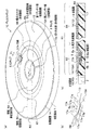
《ディスクメディアの基本的構造》
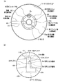
図1の(a)に示すディスクメディア1Aは、CDやDVDなどの一般的な光ディスクメディアに共通である以下のような基本的構造を有している。すなわち、このディスクメディア1Aには、中心部に中心孔2が設けられており、ディスクメディア1Aは、プレーヤに挿入されたときにはこの中心孔2を中心に回転され、情報記録面にレーザ光が照射されて、その反射光の光量に応じて信号が読み取られる。また、この中心孔2から所定距離分だけ外側の領域R1には、樹脂基板7上にAg、Alなどの導電性材料からなる数十ナノメートル(nm)程度の厚さの金属膜層(金属膜領域)14(図1の(c)参照)が成膜されている。そして、金属膜層14が成膜された領域R1のうち、内縁部側の領域R2および外縁部側の領域R3を除く内側が、情報記録領域R4とされている。ここでは、外縁部側の領域R3は、金属膜層14が成膜されていない場合の例で図示してある。内縁部側の領域R2は、以下、情報非記録領域R2と称する。図1の(a)では、二点鎖線の円で情報非記録領域R2と情報記録領域R4の境界を示す。図1の(c)に示すように、金属膜層14の表面は、保護層8でコーティングされたものとなっている。
<Basic structure of disc media>
A disk medium 1A shown in FIG. 1A has the following basic structure common to general optical disk media such as CD and DVD. That is, the disc medium 1A is provided with a
金属膜層14の上に形成する保護層8には、接着剤としても使用される、例えば、紫外線硬化樹脂などが用いられ、スピンコート法などによって塗付される。例えば、半径15〜60mmの範囲に紫外線硬化樹脂を塗布すれば、膜厚30nmの保護層を形成することができる。
ディスクメディア1AがCDであるときは、樹脂基板7、金属膜層14、保護層8を含めた厚さは約1.2mm程度である。
The
When the disc medium 1A is a CD, the thickness including the
なお、現在一般的に使用されているCD、DVDは、その直径が12cmとなっている。そして、金属膜層14(図1の(c)参照)が成膜された領域R1は、中心を基準として直径25mm〜119mmとされ、そのうち、情報記録領域R4は直径44mm〜117mmとされている。ただし、中心孔2の周りでは、クランピング領域が通常、中心から直径36mmまでとされている。また、小型の光ディスクメディアもあり、その直径は最小で6cm程度となっている。
Note that the diameter of CDs and DVDs that are currently used generally is 12 cm. The region R1 where the metal film layer 14 (see FIG. 1C) is formed has a diameter of 25 mm to 119 mm with respect to the center, and the information recording region R4 has a diameter of 44 mm to 117 mm. . However, around the
なお、中心孔2の径方向外方側のクランピング領域も含む領域に金属膜層14が形成されている場合もあるので、ここでは、クランピング領域、金属膜層14が成膜された領域R1の境界と関係無く、中心方向から径方向外方側に向かって、金属膜層14が成膜されていない非成膜部16で構成された領域を中心非成膜領域R5と称し、金属膜層14が成膜され、データが記録されていない径方向領域を情報非記録領域R2と称し、金属膜層14が成膜され、情報が記録されているかまたは情報を記録可能な径方向領域を情報記録領域R4と称することにする。一般に称される前記クランピング領域は、金属膜層が成膜されていない中心非成膜領域R5よりなる場合もあるし、金属膜層が成膜された領域R1までも含む場合もある。
Since the
なお、金属膜層14の材料は、Al、Ag、Au、Ni、Cr、Cu、Al−Cu、Al−Pd−Cu、Ag−Pd−Tiなどであるが、特に、Al、Ag、Au系の合金材料を用いることが望ましい。また、金属膜層14の厚さを50nm以上とすることによって電波の反射率を高くすることができる。例えば、異方性が高いスパッタリングによって金属膜層14を形成すれば、140nm程度の厚さの膜厚を形成することができる。それ以外に真空蒸着法、インクジェット方式による印刷などの方法によっても金属膜層14を形成することもできる。
The material of the
《第1の実施形態》
まず、図1を参照しながら第1の実施形態のディスクメディアについて説明する。図1の(a)は、本実施形態のディスクメディアであるCDの概略的な構成を示す上面図であり、(b)は(a)におけるA1部の拡大上面図であり、(c)は(a)におけるY1−Y1拡大断面図である。
<< First Embodiment >>
First, the disk medium of the first embodiment will be described with reference to FIG. FIG. 1A is a top view showing a schematic configuration of a CD that is a disk medium of the present embodiment, FIG. 1B is an enlarged top view of a portion A 1 in FIG. FIG. 3 is an enlarged view of Y 1 -Y 1 in (a).
本実施形態では、前記のような基本的構造に対して、中心孔2の近傍周縁領域には、金属膜層14が成膜されていない、つまり、非成膜部16により構成された径方向幅、約0.5mmの中心非成膜領域(非成膜領域)R5が設けられ、その外側の金属膜層14が成膜された情報非記録領域R2に、直径、約30mmの金属膜層14が成膜されていない非成膜部16(図1の(c)参照)により構成された環状スロット(非成膜領域)6Aが設けられている。環状スロット6Aの幅L1は、後記する信号入出力電極(アンテナへの給電用の端子)5a、5bの間隔に対応した幅である。環状スロット6Aにより、金属膜層14が成膜された領域R1が、環状スロット6Aの外側領域である第1アンテナ部(金属膜領域)13と、環状スロット6Aの内側領域である第2アンテナ部(金属膜領域)15Aとに、電気的に分離される。さらに、前記第2アンテナ部15Aには、金属膜層14が成膜されていない非成膜部16で構成された切り欠き部15aが径方向に、中心非成膜領域R5と環状スロット6Aとが非成膜部16でつながるように設けられている。つまり、第2アンテナ部15Aは、金属膜層14でCの字型に成膜された平面形状をした領域で構成されている。
In the present embodiment, with respect to the basic structure as described above, the
金属膜層14をスパッタリングにより成膜する段階で、マスキングすることによりディスクメディア1Aの情報非記録領域R2の情報記録領域R4との境界付近の金属膜層14に、図1の(a)に示すように、環状スロット6A、切り欠き部15a、中心非成膜領域R5を形成する。その環状スロット6Aを内外に跨ぐようにして、破線で示した5a、5bの位置に、ICチップ5のアンテナへの給電用の端子である信号入出力電極5a、5bが対応するように、つまり図1の(c)に示すようICチップ5を搭載する。
FIG. 1A shows the
信号入出力電極5a、5bは、例えば、Au製のパッドで構成されており、例えば、超音波接合、金属共晶などにより金属膜層14と信号入出力電極5a、5bとを接合する。信号入出力電極5a、5bは、金属膜層14と異方性導電膜を介して接続しても良い。そして、金属膜層14の表面にICチップ5を搭載した後に、保護層8で金属膜層14の表面をコーティングする。
The signal input /
このような構成により、金属膜層14が成膜された領域R1に含まれる環状スロット6Aは、受信した電界を定在波として共振させて増幅する、ループアンテナに対応するスロットアンテナとして機能する。そしてICチップ5は、このスロットアンテナにより外部のR/Wとの間で無線通信を行なうことが可能となる。
With such a configuration, the
なお、環状スロット6Aを形成してICチップ5を搭載した部分の径方向領域は、情報の記録に使えないので、この部分の径方向領域は情報非記録領域R2に含まれることが望ましい。さらに好適なのは、当該ディスクメディア1Aの規格における情報非記録領域R2で、かつ、非クランピング領域であることである。
Note that the radial region of the portion where the
なお、環状スロット6Aの周長は、通常のループアンテナと同様に、通信波長の1波長分となるときに通信が最も良くなる。例えば、本実施形態では2.45GHzの通信波長に対して適した環状スロット6Aの周長になっている。
Note that communication is best when the circumferential length of the
発明者らの計測によると、ICチップ5の信号入出力電極5a、5bを、環状スロット6Aの径方向内外方の両側に位置する金属膜層14の領域にそれぞれ電気的接続するときに、接続位置の切り欠き部15aとの周方向相対位置、つまり、切り欠き部15aに対するICチップ5の搭載位置の周方向角度によって、アンテナのインピーダンスが変化することが分かったので、このことを利用してICチップ5とアンテナのインピーダンスマッチングを取ることができる。また、環状スロット6Aの周長が1波長よりも短い場合でも、ICチップ5の環状スロット6Aに対する搭載位置を最適化すること、即ちICチップ5とアンテナのインピーダンスマッチングを取ることにより、ICチップを効率よく動作させることができ、良好な通信を行うことができる。
前記周方向相対位置によるインピーダンス変化を具体的に説明すると、切り欠き部15aを設けてある周方向位置の180°反対側の周方向位置を基準の0°とし、左周り、右回りに−180°、+180°とすると、インピーダンスは0°と±約90°に極大値を有し、±45°と±180°より少し手前側(0°寄り)に極小値を有する連続変化曲線である。
According to measurement by the inventors, when the signal input /
The impedance change due to the relative position in the circumferential direction will be described in detail. The circumferential position on the opposite side of the circumferential position where the
(第1の実施形態の効果)
本実施形態によれば、ディスクメディア1Aは、金属膜層14に環状スロット6Aを設けて金属膜層14が成膜された領域R1をICチップ5のアンテナとして使用でき、感度の良いアンテナを形成できる。そして、切り欠き部15aとICチップ5との周方向相対位置でアンテナとICチップ5とのインピーダンスマッチングを行なっているので、ICチップ5側に特別なインピーダンスマッチング回路を作る必要がない。この結果、ICチップ5を用いたRFIDタグ全体として、小面積のものとすることができる。また、金属膜層14をアンテナとして利用し、新たな部材を追加していないので、従来のICチップ搭載型のディスクメディアに対してコストアップする要因はない。
また、広範囲にわたる金属膜層14が成膜された領域R1がアンテナとなるのでR/Wに対して広い読み取り/書き込みエリアを提供できる。特に、情報非記録領域R2の情報記録領域R4との境界近傍、クランピング領域よりも径方向外方側に環状スロット6Aを設けているので、ディスクメディアの読取装置の内部で再生あるいは記録中に通信を行なうことも可能である。
(Effects of the first embodiment)
According to the present embodiment, the disc medium 1A can use the region R1 in which the
Further, since the region R1 where the
また、上記のような、デジタルコンテンツの著作権管理等の利用だけでなく、銀行の顧客情報や、取引情報等の、高付加価値の情報の改ざんや不正コピーを防止することにも利用することができる。 In addition to the use of digital content copyright management as described above, it is also used to prevent tampering and unauthorized copying of high-value-added information such as bank customer information and transaction information. Can do.
本実施形態における環状スロット6Aまたは切り欠き部15aの形成は、金属膜層14を成膜するときに前記のようなマスキングすることによって実現することもできるし、樹脂基板7に金属膜層14を成膜した後に環状スロット6A、切り欠き部15aとなる部分の金属膜層14をレーザ加工などにより除去することによって実現することもできる。
The formation of the
また、本実施形態では、第1アンテナ部13にディスクメディアの情報記録領域が含まれるものとしたが、第2アンテナ部15Aにディスクメディアの情報記録領域が含まれるように構成しても良い。そのような構成により、スロット周長が変わり、異なった周波数に対応することが可能となる。
In the present embodiment, the
《第1の実施形態の第1の変形例》
次に、図2を参照しながら第1の実施形態の第1の変形例について説明する。図2は、本実施形態の第1の変形例のディスクメディア1BであるCDの概略的な構成図であり、(a)は上面図、(b)は(a)のA2部拡大図である。
第1の実施形態と異なるところは、図2の(b)に示すように環状スロット(非成膜領域)6Bの外径が30mm、幅L2が略4mmと、環状スロット6Bの幅L2を第1の実施形態における環状スロット6Aの幅L1より広くし、ICチップ5を搭載する部分に狭隘部6aを設けて、信号入出力電極5a、5bが環状スロット6Bを内外に跨ぐことができるようにしてある点である。第1の実施形態と同じ構成については同じ符号を付し、重複する説明を省略する。
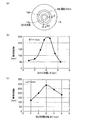
このように、環状スロット6Bの幅L2を広くすることにより、通信可能距離の向上することが発明者によって確認されている。図3の(b)に示すようにディスク1枚において、環状スロット6Bの幅L2に対する通信可能距離の変化を測定した結果によると、通信可能距離はスロット幅L2が4mmのときに一番良いということがわかった。
また、通信可能距離が長くなる効果に加えて、スロット幅L2は電波の通過し易さにも影響を及ぼす。その結果、複数枚重ねた場合、電波の通りやすさの寄与が、幅が広過ぎることによるデメリットより大きくなるので、ディスクを重ねた状態での通信可能距離は、図3の(b)に示した4mm付近にある通信可能距離の極大値に対応するスロット幅L2がより大きい値へシフトする。その結果、重ねる枚数が多い場合は、スロット幅L2を5mmとすると良い。
また、図3の(c)に示すように、切り欠き部15aの幅W1は、3mmのときに一番通信可能距離が長くなるという結果が出た。
<< First Modification of First Embodiment >>
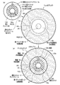
Next, a first modification of the first embodiment will be described with reference to FIG. Figure 2 is a schematic block diagram of a CD is a disk medium 1B according to the first modification of this embodiment, (a) is a top view, (b) in A 2 an enlarged view of part (a) is there.
The difference from the first embodiment is that the outer diameter of the annular slot (non-deposition region) 6B is 30 mm, the width L2 is approximately 4 mm, and the width L2 of the
As described above, the inventor has confirmed that the communicable distance is improved by increasing the width L2 of the
In addition to the effect of increasing the communicable distance, the slot width L2 also affects the ease of passage of radio waves. As a result, when multiple sheets are stacked, the contribution of the ease of passing radio waves is greater than the demerit of being too wide, so the communicable distance with the disks stacked is shown in FIG. The slot width L2 corresponding to the maximum value of the communicable distance in the vicinity of 4 mm is shifted to a larger value. As a result, when the number of stacked sheets is large, the slot width L2 is preferably set to 5 mm.
Further, as shown in FIG. 3C, when the width W1 of the
《第1の実施形態の第2の変形例》
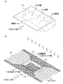
次に、図4を参照しながら第1の実施形態の第2の変形例について説明する。図4は、本実施形態の第2の変形例のディスクメディア1CであるCDの概略的な構成図であり、(a)は上面斜視図、(b)は凹部の拡大図、(c)は(a)におけるY2−Y2拡大断面図である。
第1の実施形態の第1の変形例が、ICチップ5を平坦な樹脂基板7上の金属膜層14の表面に搭載したものであるのに対し、本変形例は、ディスクメディア1Cの樹脂基板7に凹部17Aを形成して、その後に金属膜層14を成膜し、ICチップ5を凹部17Aの底面の金属膜層14の表面に搭載したものである。第1の実施形態の第1の変形例と同じ構成については同じ符号を付し、説明を省略する。
凹部17Aの深さは、ICチップ5の厚さと後記する異方性導電膜9の膜厚との合計の厚さに略一致し、例えば、100μmぐらいである。図4の(b)に示すように、凹部17Aの平面形状は、ICチップ5の平面形状と略相似な正方形または長方形であり、凹部17Aの4辺の側壁は底面17bに向かう傾斜面17aであり、成膜する前に、凹部17Aの周方向に延びる傾斜面17aおよび底面17bの狭隘部6aに対応する部分を含む環状スロット6Bにマスキングをして金属膜層14を成膜する。その結果、図4の(c)では、凹部17Aの傾斜面17aと底面17bの符号を省略してあるが、凹部17Aの傾斜面17aおよび底面17bにも狭隘部6aを残して金属膜層14が成膜される。
<< Second Modification of First Embodiment >>
Next, a second modification of the first embodiment will be described with reference to FIG. 4A and 4B are schematic configuration diagrams of a CD that is a disc medium 1C according to the second modification of the present embodiment, in which FIG. 4A is a top perspective view, FIG. 4B is an enlarged view of a recess, and FIG. it is a Y 2 -Y 2 enlarged sectional view of (a).
Whereas the first modification of the first embodiment is such that the
The depth of the
次に、凹部17Aの底面に形成された金属膜層14の表面に異方性導電膜9を塗布し、この凹部17Aの底面にICチップ5を載せて押圧することにより、ICチップ5の信号入出力電極5a、5bは、凹部17Aの底面に形成された非成膜部16の狭隘部6aを跨いで金属膜層14と電気的に接続される。そして、金属膜層14が成膜された領域R1の全面にコーティングして保護層8を形成する(図4の(b)参照)。
Next, the anisotropic
《第1の実施形態の第3の変形例》
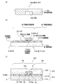
次に、図5および図6を参照しながら第1の実施形態の第3の変形例について説明する。本変形例のディスクメディア1DであるCDの概略的な構成図を示す斜視上面図は、図4の(a)と略同じであり省略した。図5は、図4の(a)のY2−Y2拡大断面図に対応する図である。
本変形例は第1の実施形態の第2の変形例を基本にしたものであり、第1の実施形態の第2の変形例と異なる点は、図6の(a)、(b)に示すように凹部17Aの底面には溝18がさらに周方向に延びるように形成されている点である。図6の(b)は(a)におけるX1−X1拡大断面図であり、(c)は凹部および溝への異方性デポジションの作用を説明する図である。第1の実施形態の第2の変形例と同じ構成については同じ符号を付し、重複する説明を省略する。
溝18の深さは凹部17Aの底面17bから、例えば、100μmぐらいで、溝18の側壁は略垂直または溝18の底面18dが広くなるような逆テーパ状の垂直側壁18bである。溝18は凹部17Aの周方向の傾斜面17aの左右周方向に延びている。溝18は左右周方向に延びるに従い、幅が広くなり、最後は環状スロット6Bの幅と同じ幅となり、深さは浅くなっていく傾斜面18cを有して略垂直の垂直壁18aで閉じている。
<< Third Modification of First Embodiment >>
Next, a third modification of the first embodiment will be described with reference to FIGS. A perspective top view showing a schematic configuration diagram of a CD which is the disc medium 1D of this modification is substantially the same as (a) of FIG. 4 and is omitted. FIG. 5 is a diagram corresponding to the Y 2 -Y 2 enlarged sectional view of FIG.
This modification is based on the second modification of the first embodiment, and the points different from the second modification of the first embodiment are shown in FIGS. 6 (a) and 6 (b). As shown, a
The depth of the
図6の(c)に示すように、環状スロット6Bの部分をダブルハッチングで示したフォトレジスト19でマスキングし、樹脂基板7の略鉛直上方から異方性デポジション(スパッタリング)によって金属膜層14を成膜すると、樹脂基板7の上面、凹部17Aの4辺の傾斜面17aおよび底面17b、溝18の傾斜面18cおよび底面18dには、膜厚が50〜250nm(0.05〜0.25μm)の厚さで金属膜層14が成膜される。しかし、成膜時の異方性デポジションは直進性が強いので、溝18の垂直壁18aおよび対向する垂直側壁18bの部分には金属膜層14は成膜されない。
したがって、成膜された金属膜層14は、狭隘部6aを構成する溝18の垂直壁18aおよび対向する垂直側壁18b、ならびに環状スロット6Bの幅広の本体部分で径方向内外方に分離されるので、電気的に分離された第1アンテナ部13と第2アンテナ部15Aとを形成することができる。
As shown in FIG. 6C, the portion of the
Therefore, the formed
《第1の実施形態の第4の変形例》
次に、図7および図8を参照しながら第1の実施形態の第4の変形例について説明する。本変形例のディスクメディア1EであるCDの概略的な構成図を示す斜視上面図は、図4の(a)と略同じであり省略した。図7は、図4の(a)のY2−Y2拡大断面図に対応する図である。
本変形例は第1の実施形態の第2の変形例を基本にしたものであり、第1の実施形態の第2の変形例と異なる点は、図8の(a)、(b)に示すように凹部17Bの形状が第1の実施形態の第2の変形例における凹部17Aと異なる点と、ICチップの信号入出力電極5a、5bが上下の面に設けられたICチップ5Aを用いている点である。第1の実施形態の第2の変形例と同じ構成については同じ符号を付し、重複する説明を省略する。
凹部17Bの深さは、ICチップ5の厚さと異方性導電膜9の膜厚の2倍との合計の厚さに略一致し、例えば、100μmぐらいである。凹部17Bの平面形状は、ICチップ5Aの平面形状と略相似な正方形または長方形であり、凹部17Bの径方向に向かい合う2辺の側壁の一方のみ、ここでは、径方向内方側の側壁は底面17bに向かう傾斜面17aであり、残りの3辺の側壁は略垂直の垂直面17cである。成膜する前に、環状スロット6Bの広幅の本体部分に図8の(b)に示すように、ダブルハッチングで示したフォトレジスト19でマスキングする。
<< Fourth Modification of First Embodiment >>
Next, a fourth modification of the first embodiment will be described with reference to FIGS. A perspective top view showing a schematic configuration diagram of a CD which is the disc medium 1E of this modification is substantially the same as (a) of FIG. 4 and is omitted. FIG. 7 is a diagram corresponding to the Y 2 -Y 2 enlarged cross-sectional view of FIG.
This modification is based on the second modification of the first embodiment, and the points different from the second modification of the first embodiment are shown in FIGS. 8 (a) and 8 (b). As shown, an
The depth of the
そして、樹脂基板7の略鉛直上方から異方性デポジション(スパッタリング)によって金属膜層14を成膜すると、樹脂基板7の上面、凹部17Bの1辺の傾斜面17aおよび底面17bには、膜厚が50〜250nm(0.05〜0.25μm)の厚さで金属膜層14が成膜される。しかし、成膜時の異方性デポジションは直進性が強いので、垂直面17cの部分には金属膜層14は成膜されない。
したがって、成膜された金属膜層14は、狭隘部6aを構成する凹部17Bの垂直面17cおよび環状スロット6Bの幅広の本体部分で径方向内外方に分離されるので、電気的に分離された第1アンテナ部13と第2アンテナ部15Aとを形成することができる。
Then, when the
Therefore, the formed
次に、図7に示すように、凹部17Bの底面17bに形成された金属膜層14の表面に異方性導電膜9を塗布し、この凹部17Bの底面17bにICチップ5Aの信号入出力電極5bを下に向けて載せて押圧し、さらに、ICチップ5Aの上面(信号入出力電極5a)側とそれに隣接する凹部17Bの径方向外方側の金属膜層14の一部に異方性導電膜9を塗布し、さらに、そこに金属箔10を載せ、ICチップ5Aの上面(信号入出力電極5a)側を凹部17Bの径方向外方側の金属膜層14と電気的に接続する。そして、金属膜層14が成膜された領域R1の全面にコーティングして保護層8を形成する。
Next, as shown in FIG. 7, the anisotropic
なお、凹部17Bの径方向内方側または外方側の側壁のいずれを底面17bに向かう傾斜面17aとしても良い。底面17bおよび傾斜面17aと電気的に接続されたICチップ5Aの下側の信号入出力電極が、第1アンテナ部13または第2アンテナ部15Aのいずれかと接続されたら、ICチップ5Aの上側の信号入出力電極は、残りのアンテナ部と電気的に接続させる。
Note that either the radially inner side wall or the outer side wall of the
(第1の実施形態の第2から第4の変形例の効果)
このように図4から図8に示した第1の実施形態の第2の変形例から第4の変形例のように、ICチップ5、またはICチップ5Aを樹脂基板7の厚さ方向の内部に埋め込むことにより、ディスクメディア1C、1D、1Eにおける金属膜層14が成膜された領域R1の表面を、第1の実施形態およびその第1の変形例の場合よりもより平坦にすることができるので、ディスクメディア1Cからディスクメディア1Eの保護層8の上面におけるディスク駆動装置との機械的クリアランスを大きくすることができる。
(Effects of the second to fourth modifications of the first embodiment)
As described above, as in the second to fourth modifications of the first embodiment shown in FIGS. 4 to 8, the
《第1の実施形態のその他の変形例》
なお、第1の実施形態およびその変形例においては、第2アンテナ部15Aに非成膜部16で構成された切り欠き部15aを設けるものとしたが、それに限定されない。ICチップ5またはICチップ5Aがインピーダンスマッチング回路を内蔵している場合は、図9に示すディスクメディア1Fのように第2アンテナ部15Bは、金属膜層14が成膜された単なる環状の領域でも良い。図9は幅L1の狭い環状スロット6Aの場合を例示したものであり、それに限定されること無く、幅広の環状スロット6Bとし、ICチップ5またはICチップ5Aを前記した狭隘部6aに搭載するようにしても良い。この場合、ICチップ5、5Aは、環状スロット6A、6Bの周方向の任意の位置に配置できる。
<< Other Modifications of First Embodiment >>
In the first embodiment and the modification thereof, the
《第2の実施形態》
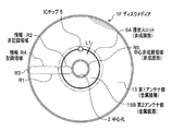
次に、図10から図12を参照しながら第2の実施形態のディスクメディアについて説明する。図10は、本実施形態のディスクメディア1Gの概略的な構成図であり、(a)は上面図、(b)は(a)におけるB1部拡大図であり、(c)ICチップの信号入出力電極面を示す平面図、(d)は小型インレットのアンテナ部分を示す平面図である。図11の(e)は図10の(a)におけるY3−Y3拡大断面図であり、(f)は小型インレットの等価回路を説明する図である。
図12は、本実施形態における別の形状の小型インレットを適用したディスクメディア1Hの概略的な構成図であり、(a)は上面図、(b)は(a)におけるB2部拡大図である。
第1の実施形態の第1の変形例がICチップ5を、金属膜層14を成膜した情報非記録領域R2の金属膜層14の表面に直に搭載したディスクメディア1Bであったのに対し、本実施形態のディスクメディア1G、1Hは、金属膜層14を成膜した情報非記録領域R2にICチップ5と、小型アンテナ23Aまたは小型アンテナ23Bと、を備えてなる小型インレット11Aまたは小型インレット11Bを搭載したものである。本実施形態では、第1の実施形態の第1の変形例と異なり、環状スロット6Bは、ICチップ5の信号入出力電極5a、5bと電気的接続するための狭隘部6aを有せず、全周に亘り幅L2がICチップ5の幅よりも広い3mmである。第1の実施形態の第1の変形例と同じ構成については同じ符号を付し、重複する説明を省略する。
<< Second Embodiment >>
Next, a disk medium according to the second embodiment will be described with reference to FIGS. Figure 10 is a schematic diagram of a disk medium 1G according to this embodiment, (a) shows the top view, (b) is a part enlarged view B in (a), (c) IC chip signal FIG. 4D is a plan view showing an input / output electrode surface, and FIG. 4D is a plan view showing an antenna portion of a small inlet. FIG. 11E is an enlarged Y 3 -Y 3 sectional view of FIG. 10A, and FIG. 11F is a diagram for explaining an equivalent circuit of a small inlet.
Figure 12 is a schematic diagram of a disk medium 1H applying the small inlet of another shape in the present embodiment, (a) is a top view, (b) is a B 2 parts enlarged view of (a) is there.
Although the first modification of the first embodiment is the disk medium 1B in which the
また、本実施形態でいう小型インレットとは、ICチップと、ディスクメディアに形成したアンテナとICチップのインピーダンスマッチングを行うスリットを形成することができる長さおよび幅の小型アンテナと、を有し、ベースとなるフィルムなどの上にこれらを固定したものをいう。
通常であれば、インレットのアンテナ長は、樹脂基板上での誘電率を考慮した通信に用いる電波の波長λの半分の長さとする。しかし、アンテナをそれよりも短くした小型インレットを使用し、サイズの縮小を優先することができる。インレットのアンテナの長さが波長λの半分以下の長さであっても、インピーダンスマッチングが取れれば、小型インレット単体で、または他の金属部材(本実施形態では金属膜層が対応)との作用により、R/Wとの通信が可能となる。
図10の(b)に示すように、小型インレット11Aは、Alなどの電気導体の金属薄膜で構成された直線形状の小型アンテナ23Aが、例えば、ポリエチレンテレフタレート(PET)よりなるベースフィルム21(絶縁体)の表面に成膜、印刷などにより形成され、小型アンテナ23Aの中央部分にL字型のスリット23aが形成され、そのスリット23aを跨いでICチップ5の信号入出力電極5a、5bが、超音波接合、共晶接合、異方性導電膜を介してなどにより小型アンテナ23Aと電気的に接続するように搭載されたものである。小型インレット11Aは、長さが5〜15mmと、送受信に用いられる電波の樹脂基盤上での誘電率を考慮した電気的波長を、λとしたとき、波長λの0.04λ〜0.14λ程度の長さである。このような構成の小型インレット11Aは、(a)に示すように、ディスクメディア1Gの情報非記録領域R2の表面に、ベースフィルム21の裏面に塗付された粘着材22(図11の(e)参照)により貼り付けられ、搭載される。このとき小型アンテナ23Aの両方の端部23bがベースフィルム21を介して金属膜層14と静電容量結合で接続されている。本実施形態では、「小型アンテナの所定箇所」として小型アンテナ23Aの一方の端部23bが、第1アンテナ部13の金属膜層14と、他方の端部23bが、第2アンテナ部15Aの金属膜層14と静電容量結合によって接続している。
なお、小型インレット11Aを貼り付けるとき、小型アンテナ23Aのスリット23aの部分が情報非記録領域R2の金属膜層14に重なったりしないように配置することが好ましい。
In addition, the small inlet referred to in the present embodiment has an IC chip, a small antenna having a length and a width that can form an antenna formed on a disk medium and a slit for impedance matching of the IC chip, This means a film that is fixed on a base film.
Normally, the antenna length of the inlet is half the wavelength λ of the radio wave used for communication in consideration of the dielectric constant on the resin substrate. However, it is possible to give priority to size reduction by using a small inlet with a shorter antenna. Even if the length of the inlet antenna is less than half of the wavelength λ, if impedance matching can be achieved, the small inlet alone or other metal member (in this embodiment, the metal film layer is compatible) Thus, communication with the R / W becomes possible.
As shown in FIG. 10B, the
When the
図10の(d)に示すように、ICチップ5の信号入出力電極5a、5bを、L字型のスリット23aのL字のコーナ部で跨いだ両側に位置する小型アンテナ23Aにそれぞれ電気的に接続することによって、スリット23aの形成によってできたスタブ23cの部分を、アンテナとなる小型アンテナ23Aの他の部分、第1アンテナ部13および第2アンテナ部15Aと、ICチップ5と、の間に直列に接続することになり、スタブ23cの部分が直列に接続したインダクタ成分として働く(図11の(f)参照)。このインダクタ成分により、ICチップ5内のキャパシティブ成分を相殺し、小型アンテナ23Aの他の部分、第1アンテナ部13および第2アンテナ部15Aと、ICチップ5のインピーダンスマッチングを取ることができる。つまり、ICチップ5は十分な面積の金属膜層14に形成された環状スロット6Bを、ループ型アンテナに対応するスロットアンテナとして機能させることができると共に、ICチップ5のインピーダンスとスロットアンテナのインピーダンスをマッチングさせることができる。このようなスリット23aをインピーダンスマッチング回路と称する。
なお、ICチップ5とアンテナとなる小型アンテナ23Aの残りの部分および金属膜層14とのインピーダンスマッチングはスリット23aのL字型のコーナまでの各長さによって決まるスタブ23cの面積により決定される。
As shown in FIG. 10 (d), the signal input /
The impedance matching between the
小型インレットは直線形状に限定されるものではなく、図12に示すように、L字形状の小型インレット11Bでも良い。また、図示しないが両端に耳をもつコの字形状のものでも良い。ただ、小型アンテナの両端の端部の一方が、環状スロット6Bの径方向内方側および外方側の内のいずれかの側の金属膜層14と静電容量結合し、小型アンテナの端部の他方が、環状スロット6Bの径方向内外方の内の他方の側の金属膜層14と静電容量結合していれば良い。
L字形状の小型インレット11B、コの字型の小型インレットとすると、端部の静電容量結合部分の面積が増すので、アンテナ効率が増大する。また、小型インレットを用いることにより、環状スロット6Bに狭隘部6aを設ける必要が無く、環状スロット6Bの形状が簡単になる。
The small inlet is not limited to a linear shape, and may be an L-shaped
If the L-shaped
本実施形態によれば、第1の実施形態の第1の変形例と同じ効果が得られ、さらに、小型インレット11A、11Bがインピーダンスマッチング回路を有しているので、第2アンテナ部15Aに切り欠き部15aを設ける必要がなくなる可能性がある。
また、本実施形態では、インピーダンスマッチング回路としてL字型のスリット23aとしたがそれに限定されるものではなく、他の形状でも良い。例えば、L字型のスリット23aの代わりにT字型スリットとしても良い。その場合、T字の縦棒部分が小型アンテナ23Aまたは小型アンテナ23Bの幅方向に、T字の横棒部分を小型アンテナ23Aまたは小型アンテナ23Bの長手方向になるように形成し、スリットのT字型のコーナ部に、T字の縦棒を跨ぐように、アンテナへの給電用の端子である信号入出力電極5a、5bを対応させてICチップ5を搭載する。
According to the present embodiment, the same effect as that of the first modification of the first embodiment can be obtained, and furthermore, since the
In this embodiment, the L-shaped
なお、本実施形態では前記したように、小型インレット11A、11Bのスリット23aを金属膜層14と重ならないように位置させることが望ましいとしたが、環状スロット6Bの幅が小さく、スリット23aが金属膜層14と重なる場合にも、小型インレット11A、11Bを搭載する位置と、切り欠き部15aとの相対周方向位置によってもインピーダンスマッチングを行なえる。
In the present embodiment, as described above, the
《第2の実施形態の変形例》
次に図13および図14を参照しながら本実施形態の変形例を説明する。本変形例は、第2の実施形態において、情報非記録領域R2に凹部17Cを設け、そこに小型インレット11Aを搭載したものである。図13および図14は、本変形例のディスクメディア1KであるCDの概略的な構成図であり、図13の(a)は斜視上面図であり、図14の(b)は図13の(a)のB3部の凹部の拡大図、図14の(c)は図13の(a)におけるY4−Y4拡大断面図である。
直線形状の小型インレット11Aは、前記図10の(b)に示した構成と同じである。図13の(a)に示すように、樹脂基板7に、小型インレット11Aの平面形状に略一致する凹部17Cを情報非記録領域R2に径方向に長く形成する。凹部17Cの4辺の側壁は、図14の(b)に示すように、底面17bに向かう傾斜面17aを有している。そして、二点鎖線の想像線で示すように金属膜層14を成膜後、小型インレット11Aを凹部17Cに貼り付ける。その際、図14の(c)に示すように小型アンテナ23Aの両側の端部23bを、ベースフィルム21を介して、第1アンテナ部13の金属膜層14および第2アンテナ部15Aの金属膜層14それぞれに静電容量結合で接続する。
なお、小型インレット11Aを貼り付けるとき、小型アンテナ23Aのスリット23aの部分が金属膜層14と重なったりしないように配置することが望ましい。
<< Modification of Second Embodiment >>
Next, a modification of the present embodiment will be described with reference to FIGS. In this modification, in the second embodiment, a
The linear
It should be noted that when the
なお、本変形例では小型インレットの形状を直線形状の小型インレット11Aを例に説明したが、それに限定されるものではなく他の形状の小型インレットとしても良い。
例えば、図12の(b)に示したようなL字形状の小型インレット11Bでも良い。また、図示しないが両端に耳をもつコの字形状のものでも良い。ただ、凹部17Cの形状は、小型インレットの形状に合わせた平面形状とする。
In the present modification, the shape of the small inlet is described by taking the linear
For example, an L-shaped
(第2の実施形態およびその変形例の効果)
本実施形態またはその変形例によれば(図10〜図15参照)、金属膜層14が成膜された領域R1がアンテナの機能をするので、例えば、小型インレット11A、11Bは長さが5〜15mmと短いもので良く、インピーダンスマッチング用のスリット23aを形成された小型アンテナ23Aによって構成することができる。したがって、小型インレット11A、11Bはきわめて小さくすることができる。
本実施形態およびその変形例によれば、例えば、小型インレット11A、11Bの小型アンテナ23A、23Bの両側の端部23bは金属膜層14に静電容量結合で接続され、金属膜層14が成膜された領域R1をアンテナとして使用できる。
その効果は、第1の実施形態およびその変形例で記載の場合と同じ効果が得られる。つまり、ディスクメディア1G、1H、1Kに搭載されたRFIDタグとしての小型インレットは、金属膜層14が成膜された領域R1をICチップ5のアンテナとして使用でき、小型アンテナ23A、23Bと併せて、感度の良いアンテナを形成できる。また、金属膜層14をアンテナとして利用し、新たな部材を追加していないので、従来のICチップ搭載型のディスクメディアに対してコストアップする要因はない。
また、広範囲にわたる金属膜層14がアンテナとなるのでR/Wに対して広い読み取り/書き込みエリアを提供できる。
(Effect of 2nd Embodiment and its modification)
According to the present embodiment or a modification thereof (see FIGS. 10 to 15), the region R1 where the
According to this embodiment and its modification, for example, the
The effect is the same as that described in the first embodiment and its modifications. That is, the small inlet as the RFID tag mounted on the disk media 1G, 1H, and 1K can use the region R1 on which the
Further, since the
特に、本実施形態の変形例によれば、例えば、小型インレット11A、11Bを貼り付けた後の上面側の平坦度を第2の実施形態より向上でき、保護層8の上面におけるディスク駆動装置との機械的クリアランスを大きくすることができる。
In particular, according to the modification of the present embodiment, for example, the flatness on the upper surface side after the
《第3の実施形態》
次に、図15および図16を参照しながら、第3の実施形態について説明する。前記した第2の実施形態において、小型インレット11A、11Bを、保護層8を施した後に貼り付けても良い。その場合、図15に示すように、既存の完成済みのディスクメディア(以下、元ディスクと称する)1LaをRFID付のディスクメディア1Lに低コストで生まれ変わらせることができる。
以下に、小型インレット11Aを例に詳細に本実施形態について説明する。第2の実施形態と同じ構成については同じ符号とし、重複する説明を省略する。
<< Third Embodiment >>
Next, a third embodiment will be described with reference to FIGS. 15 and 16. In the second embodiment described above, the
Hereinafter, the present embodiment will be described in detail by taking the
図15の(a)に示すように、小型インレット11Aと、例えば、Al箔で構成されたC字型の第2アンテナ部(環状の金属薄膜)15Cと、を搭載した環状スロットアンテナシール(シール)12を、すでに保護層8を施された元ディスク1Laに貼り付けて、図15の(b)に示すようにディスクメディア1Lを構成する。図16の(a)は環状スロットアンテナシールを示す平面図であり、(b)は(a)におけるY5−Y5拡大断面図である。
図15の(a)に示すように、元ディスク1Laは、中心孔2の中心から、例えば15mmまでが金属膜層14が成膜されていない非成膜部16で構成された中心非成膜領域R5、その径方向外方側に金属膜層14が成膜された領域R1と、なっている。
図16に示すように、環状スロットアンテナシール12は、図示しない粘着材を下面に塗布し、中央に中心孔26aを設けた円盤状の保護フィルム26を、保護フィルム26の所定位置に配置した小型インレット11Aと、Al箔で構成された、切り欠き部15aを有する環状の第2アンテナ部15Cと、を含むように、前記粘着材の下側に貼り付け、さらに、保護フィルム26の形状に合わせて粘着材22を塗付した剥離紙25と貼り付けたものである。
As shown in FIG. 15 (a), an annular slot antenna seal (seal) on which a
As shown in FIG. 15 (a), the original disk 1La has a central non-film-forming portion constituted by a non-film-forming
As shown in FIG. 16, the annular slot antenna seal 12 is a small type in which an adhesive material (not shown) is applied to the lower surface and a disk-shaped
なお、中心孔26aは元ディスク1Laの中心孔2と同じ径である。第2アンテナ部15Cは、例えば、外径が24mm、内径が16mmであり、保護フィルム26の内径15mmの中心孔26aと同心となるように第2アンテナ部15Cを、保護フィルム26に配置して張り付ける。また、小型インレット11Aは、小型アンテナ23Aの向きを中心孔26aに対し、長手方向が径方向を向き、径方向内方側の端部23bが第2アンテナ部15Cの下に重なるように配置する。さらに、このとき小型インレット11Aは、切り欠き部15aに対する周方向の相対位置が、インピーダンスマッチング上適切なあらかじめ設定された周方向の相対位置に設定する。また、小型インレット11Aの第2アンテナ部15Cとの重なり長さは、中心孔26aを元ディスク1Laの中心孔2に合わせたとき、小型インレット11Aの小型アンテナ23Aの径方向外方側の端部23bが、図15の(a)に示すように、情報非記録領域R2の金属膜層14に重なり、小型アンテナ23Aのスリット23a部分が金属膜層14と重ならないような配置である。
The
保護フィルム26と剥離紙25との間に、小型インレット11Aと第2アンテナ部15Cを含んで貼り付ける際、剥離紙25には中心孔26a、第2アンテナ部15Cおよび小型インレット11Aのそれぞれ位置に対応した位置に、対応した外形線図を描いておき、粘着材22を塗付済みの剥離紙25上に、小型インレット11Aの外形線図の位置に合うように小型インレット11Aを配置して貼り付ける。その後、すでに第2アンテナ部15Cを下面に貼り付けた保護フィルム26を、剥離紙25の中心孔26aの外形線図の位置と切り欠き部15aの外形線に合うように剥離紙25に貼り付けて、環状スロットアンテナシール12を製作すると良い。
When affixing between the
そして、使用時に剥離紙25を剥がして、保護フィルム26の中心孔26aが元ディスク1Laの中心孔2と合うように位置決めして、元ディスク1Laに貼り付ける。こうすることにより、精度良く、容易に小型インレット11Aを元ディスク1Laの所定の位置に搭載し、ディスクメディア1Lとすることができる。その結果、図15の(b)に示すように、環状スロットアンテナシール12の外径のすぐ外側の領域を情報記録領域R4とすることができ、金属膜層14が成膜された領域R1の内径(30mm)と第2アンテナ部15Cの外径(24mm)との間に3mm幅の環状スロット6Bが、精度よく形成されることになる。小型インレット11Aの小型アンテナ23Aの径方向外方側の端部23bは、情報非記録領域R2の金属膜層14と静電容量結合し、小型アンテナ23Aの径方向内方側の端部23bは、第2アンテナ部15CのAl箔と静電容量結合しているので、ICチップ5に対して、小型インレット11A、第1アンテナ部13および第2アンテナ部15Cは、ループ型アンテナに対応するスロットアンテナを構成していることになる。
Then, the
以上、図15、図16を用いて小型インレット11Aを例に説明したが、それに限定されるものではなく、小型インレット11Bを用いた第2の実施形態にも、また、コの字形状の小型インレットに対しても適用できる。
As described above, the
(第3の実施形態の効果)
本実施形態によれば、既存の元ディスク1Laの金属膜層14が成膜された領域R1を、簡単にループ型アンテナに対応したスロットアンテナとして利用することでき、製造が容易である。また、第2アンテナ部15Cは、例えば、C字型のAl箔で製作でき、極めて薄くできるので、クランピング領域に含まれてもディスクメディア1Lの保護フィルム26の上面におけるディスク駆動装置との機械的クリアランスにほとんど影響しない。また、環状スロットアンテナシール12は、回転の中心側にあるので、重心のずれによるアンバランスを小さくできる。
本実施形態のディスクメディア1Lの効果は、第2の実施形態およびその変形例で記載の場合と同じ効果が得られる。つまり、ディスクメディア1Lに搭載されたRFIDタグとしての小型インレット11Aは、金属膜層14が成膜された第1アンテナ部13と第2アンテナ部15CとをICチップ5のアンテナとして使用でき、小型アンテナ23Aと併せて、感度の良いアンテナを形成できる。また、広範囲にわたる金属膜層14がアンテナとなるのでR/Wに対して広い読み取り/書き込みエリアを提供できる。
(Effect of the third embodiment)
According to the present embodiment, the region R1 on which the
The effect of the disk medium 1L of the present embodiment is the same as that described in the second embodiment and its modifications. That is, the
《第4の実施形態》
次に、図17および図18を参照しながら第4の実施形態について説明する。本実施形態は第1の実施形態の第1の変形例にもとづくものであり、本実施形態が第1の実施形態の第1の変形例と異なるところは、ICチップ5の代わりにアンテナ実装型のICチップ5Bを用いて、第1アンテナ部13および第2アンテナ部15Aとは、実装アンテナが電磁界結合する点である。
図17は、本実施形態のディスクメディア1MであるCDの概略的な構成図であり、(a)は上面図、(b)はアンテナ実装型のICチップの構成を示す斜視図であり、(c)および(d)は(a)におけるB4部拡大図である。図18の(e)、(f)は図17の(a)におけるY6−Y6拡大断面図である。
本実施形態は第1の実施形態の第1の変形例と同じく、図17の(a)に示すように環状スロット6Bの外径が30mm、幅L2が3mmであり、第2アンテナ部15Aの内径は16mm、中心孔2の内径は15mmである。
<< Fourth Embodiment >>
Next, a fourth embodiment will be described with reference to FIGS. 17 and 18. This embodiment is based on the first modification of the first embodiment, and this embodiment is different from the first modification of the first embodiment in that an antenna mounting type is used instead of the
FIG. 17 is a schematic configuration diagram of a CD that is the disc medium 1M of the present embodiment, (a) is a top view, and (b) is a perspective view showing the configuration of an antenna-mounted IC chip. c) and (d) are B 4 parts enlarged view of (a). 18E and 18F are enlarged Y 6 -Y 6 sectional views in FIG.
As in the first modification of the first embodiment, this embodiment has an outer diameter of the
切り欠き部15aに対する所定の周方向の相対位置の環状スロット6Bの金属膜層14が成膜されていない非成膜部16に、アンテナ実装型のICチップ5Bを搭載する(図18の(e)参照)。ICチップ5Bは、一方の面に、例えば、この図では上面に信号入出力電極5a、5bを有し、信号入出力電極5a、5b間を渦巻状に結ぶ金属導体、例えば、Alの実装アンテナ5cを有している。ICチップ5Bは、図18の(e)に示すように、環状スロット6Bの径方向内外方向の両側の金属膜層14とわずかなギャップ、例えば1mm以下、で挟まれ、実装アンテナ5cが第1アンテナ部13および第2アンテナ部15Aと電磁界結合するようになっている。もし、ICチップ5Bの1辺の長さが環状スロット6Bの幅L2より小さい場合は、図17の(d)に示すようにICチップ5Bを配置する環状スロット6Bの部分に狭隘部6aを形成して、配置する。
第1の実施形態の第1の変形例と同じ構成については同じ符号を付し、重複する説明を省略する。
The antenna mounting
The same components as those in the first modification of the first embodiment are denoted by the same reference numerals, and redundant description is omitted.
なお、図18(e)に示すようにICチップ5Bはマスキングをして形成した非成膜部16より構成された環状スロット6Bに搭載しても良いし、その部分に図18の(f)に示すように凹部17Dを形成して、凹部17Dの底面に搭載し、ICチップ5Bを搭載しても保護層8が平坦になりようにしても良い。
このように、アンテナ実装型のICチップ5Bを環状スロット6Bに配置することによっても、金属膜層14が成膜された領域R1をループ型アンテナに対応するスロットアンテナとして機能させることができる。
As shown in FIG. 18 (e), the
As described above, by arranging the antenna-mounted
以上、第1の実施形態から第4の実施形態およびそれらの変形例によれば(図1〜図18参照)、環状スロット6A、6Bが形成され、ICチップ5、5A、5Bまたは小型インレット11A、11Bなどに搭載されたICチップ5に対して、環状スロット6A、6Bの径方向内外方の両側の第1アンテナ部13の金属膜層14、第2アンテナ部15A、15B、15Cの金属膜層14やAl箔がスロットアンテナとして機能する。
特に、情報非記録領域R2の情報記録領域R4との境界近傍、クランピング領域よりも径方向外方側に環状スロット6A、6Bを設けているので、CDをプレーヤやレコーダの内部で再生あるいは記録中に通信を行なうことも可能である。
また、環状スロット6A、6Bは周方向につながっているので、図19に示すようにディスクメディアをストッカ20に多数重ねて格納した状態でR/Wをストッカ20の上側または下側に翳すと、R/Wアンテナ28からの電波が環状スロット6A、6Bを貫いて伝播し、ストッカ20内のいずれのディスクメディアとも容易に通信を行うことができる。特許文献1に記載されたような周方向に使用波長λの1/2波長の長さのスロットを設けている場合は、多数のディスクメディアを重ねて格納するとき、そのスロットの周方向位置を各ディスクメディア間で揃えないと、電波がスロットを貫通して、各ディスクメディアのRFIDタグに届かない。そのためにディスクメディアを揃える煩雑な作業が発生する。前記各実施形態およびその変形例においては、そのような煩雑な作業が不要となる。
As described above, according to the first to fourth embodiments and their modifications (see FIGS. 1 to 18), the
In particular, since the
Further, since the
なお、前記第1の実施形態から第4の実施形態およびその変形例において、環状スロット6A、6Bの形状は、円環状として説明してきたが、それに限定されることは無く、通信波長λに対応した周長をもつ四角形などの多角形の環状スロットでも良い。
In the first to fourth embodiments and the modifications thereof, the shape of the
《第5の実施形態》
次に、図20および図21を参照しながら第5の実施形態のディスクメディアについて説明する。
本実施形態のディスクメディアは、片面にのみ金属膜層14が成膜された領域がある片面DVD30Aであり、金属膜層14をアンテナとして使用するものである。なお、片面DVD30Aは薄いCDを、樹脂基板側を外側にして、金属膜層側を向かい合わせにして貼り合わせて製造するが、この場合は一方には金属膜層が形成されており、他方は樹脂基板のまま、2枚貼り合わせた構成であるので、第1の実施形態から第4の実施形態、またはその変形例において説明した構成を用いることができる。
<< Fifth Embodiment >>
Next, a disk medium according to the fifth embodiment will be described with reference to FIGS.
The disk medium of this embodiment is a single-
図20は、第5の実施形態のディスクメディアである片面DVDにICチップを搭載する場合の構成を説明する図である。
図20の(a)に示すように、片面DVD30Aは、第1樹脂基板31aの上に金属膜層14を有する第1ディスク31Aと金属膜層14を有しない第2樹脂基板32aだけで構成された第2ディスク32Aとを貼り合わせた構成となっている。第1ディスク31A、第2ディスク32Aとも厚さは0.6mm程度であって、片面DVD30A全体の厚さはCDと同じ1.2mm程度である。異なる所は、CDなどのディスクメディア1A〜1Lでは、薄い保護層8の下に金属膜層14が形成されているのに対し、片面DVD30Aでは、ディスクの厚さ方向の略中心に金属膜層14が形成されている点である。
また、DVDなどのような2枚のディスクの貼り合わせる場合には、前記CDの金属膜層14の上に形成する保護層8に利用される、例えば、紫外線硬化樹脂が接着剤として用いられ、スピンコート法などによって塗付される。
FIG. 20 is a diagram illustrating a configuration when an IC chip is mounted on a single-sided DVD that is a disk medium according to the fifth embodiment.
As shown in FIG. 20A, the single-
Further, when two discs such as a DVD are bonded together, for example, an ultraviolet curable resin is used as an adhesive, which is used for the
図20の(b)は(a)において、第2ディスク32Aと貼り合わせる前の第1ディスク31Aを上側から見た上面図であり、(c)は(a)において、第1ディスク31Aと貼り合わせる前の第2ディスク32Aを下側から見た下面図である。図21の(a)は図20の(c)における第2ディスクのY8−Y8拡大断面図、(b)は図20の(b)における第1ディスクのY7−Y7拡大断面図、(c)は貼り合わせた後の断面図である。
このような片面DVD30Aにおいて、図20の(b)に示すように、第1ディスク31Aの金属膜層14の表面に、第2の実施形態の第1の変形例と同様に金属膜層14に環状スロット6Bを形成し、図21の(b)に示すように非成膜部16で構成された環状スロット6Bの狭隘部6aを跨いで信号入出力電極5a、5bが金属膜層14と接続するようにICチップ5を搭載する(図2の(b)参照)。一方、第2ディスク32Aの第2樹脂基板32aには、第1ディスク31Aの金属膜層14に搭載されたICチップ5に対応する位置に、図20の(c)および図21の(a)に示すようにICチップ5を収納できる大きさの凹部33Aを形成する。このように構成された第1ディスク31Aと第2ディスク32Aを貼り合わせると、図21の(c)に示すように、ICチップ5が搭載されて第1アンテナ部13および第2アンテナ部15Aの金属膜層14をループ型アンテナに対応するスロットアンテナとして機能させることができる片面DVD30Aを実現することができる。
その結果、図21の(c)に示すように、ICチップ5が片面DVD30Aの厚さ方向の中心部に装着される。
なお、第1の実施形態の第1の変形例と同じ構成については、同じ符号を付し重複する説明を省略する。
20B is a top view of the
In such a single-
As a result, as shown in FIG. 21C, the
In addition, about the same structure as the 1st modification of 1st Embodiment, the same code | symbol is attached | subjected and the overlapping description is abbreviate | omitted.
図22は、本実施形態における片面DVD30Aを構成する2枚の第1ディスク31Aおよび第2ディスク32Aを貼り合わせるための位置合せを行う位置合わせ装置の概念図である。位置合わせ装置50は、水平に第1ディスク31A、および第2ディスク32Aを載せて回転させる回転機構51に対して、光源52と撮像機能を有するCCD53が上下の両側に配置されている。位置合わせ装置50は、CCD53に接続され、第1ディスク31Aに搭載されたICチップ5の位置と第2ディスク32Aの凹部33Aの位置を検出する図示しない画像処理装置と、画像処理装置からの検出信号を受けて、第1ディスク31AのICチップ5位置と第2ディスク32Aの凹部33Aとの位置合わせを行う図示しない制御装置を有している。
なお、図22では回転機構51、光源52およびCCD53が1組だけ示されているが、実際は第1ディスク31A用および第2ディスク32A用の2組用意されている。
FIG. 22 is a conceptual diagram of an alignment apparatus that performs alignment for bonding the two
In FIG. 22, only one set of the rotation mechanism 51, the light source 52, and the
図23は、位置合わせ装置によって行われる2枚の第1ディスク31Aおよび第2ディスク32Aを貼り合わせる工程のフローチャートである。まず、第1ディスク31Aおよび第2ディスク32Aを搬送して(ステップS1)、第1ディスク31Aおよび第2ディスク32Aをそれぞれの回転機構51にクランプし(ステップS2)、光源52より光を投射してCCD53によって第1ディスク31Aの透過画像を取り込んで(ステップS3)、画像処理を行い、ICチップ5の位置を検出する(ステップS4)。次に、光源52より光を投射してCCD53によって第2ディスク32Aの透過画像を取り込んで(ステップS5)、画像処理を行い、凹部33Aの位置を検出する(ステップS6)。第1ディスク31Aに対して第2ディスク32Aの位置合わせを行う(ステップS7)。つまり、第1ディスク31AのICチップ5の位置と第2ディスク32Aの凹部33Aの位置が合うように相対的に回転して位置合わせを行う。そして、第1ディスク31Aおよび第2ディスク32Aの周方向の相対位置を固定したまま搬送アームに吸着し(ステップS8)、所定の位置に搬送した後(ステップS9)、第1ディスク31Aと第2ディスク32Aの貼り合わせを行い(ステップS10)、貼り合わせ工程が完了する。これによって、第1ディスク31Aに対して第2ディスク32Aを正確に位置合わせすることができる。
FIG. 23 is a flowchart of the process of bonding the two
《第5の実施形態における第1の変形例》
次に、図24および図25を参照しながら本実施形態の第1の変形例を説明する。
図24の(a)は、第2ディスク32Bと貼り合わせる前の第1ディスク31Bを上側から見た上面図であり、(b)は第1ディスク31Bと貼り合わせる前の第2ディスク32Bを下側から見た下面図である。図25は図24におけるY9−Y9拡大断面図、Y10−Y10拡大断面図、およびその貼り合わせ後の断面図である。
本変形例の片面DVD30Bの構成は、図24の(a)、(b)に示すように、第1ディスク31Bの金属膜層14の表面に、第2の実施形態と同様に金属膜層14が成膜された領域R1内に、非成膜部16で構成された環状スロット6Bを形成する。
<< First Modification of Fifth Embodiment >>
Next, a first modification of the present embodiment will be described with reference to FIGS. 24 and 25. FIG.
FIG. 24A is a top view of the
As shown in FIGS. 24A and 24B, the configuration of the single-sided DVD 30B of the present modification is such that the
小型インレット11Aの長手方向を径方向にし、その小型アンテナ23Aの両方の端部23bを環状スロット6Bの径方向内外方両側の金属膜層14にそれぞれ重なるように貼り付ける(図25参照)。一方、第2ディスク32Bの第2樹脂基板32aには、第1ディスク31Bに搭載された小型インレット11Aに対応する位置に、図14の(b)に示すように小型インレット11Aを収納できる大きさの凹部33Bを形成する。このように構成された第1ディスク31Bと第2ディスク32Bを貼り合わせると、図25に示すように、小型インレット11Aが搭載されて第1アンテナ部13および第2アンテナ部15Aの金属膜層14をループ型アンテナに対応するスロットアンテナとして機能させることができる片面DVD30Bを実現することができる。
その結果、図25に示すように、小型インレット11Aが片面DVD30Bの厚さ方向の中心部に装着される。
The longitudinal direction of the
As a result, as shown in FIG. 25, the
《第5の実施形態における第2の変形例》
また、図26に示すように、第2の実施形態の変形例と同様に第1ディスク31Cに小型インレット11Aを収納する凹部33Cを形成した後に、金属膜層14を成膜し、凹部33Cに小型インレット11Aを収納するように貼り付ける。この場合は、第2ディスク32Cは全く加工を施さない。このように構成された第1ディスクと第2ディスクを貼り合わせると、図26に示すように、小型インレット11Aが搭載されて第1アンテナ部13および第2アンテナ部15Aの金属膜層14をループ型アンテナに対応するスロットアンテナとして機能させることができる片面DVD30Cを実現することができる。
<< Second Modification of Fifth Embodiment >>
In addition, as shown in FIG. 26, after forming the
なお、インレットを用いる構成として第5の実施形態の変形例では前記小型インレット11Aを用いた構成としたが、これに限定されるものではない。第2の実施形態における前記小型インレット11Bを本実施形態の変形例でも用いることができる。また、他の平面形状の小型インレット、例えば、コの字型の小型インレットを用いても良い。
なお、本第1の変形例の片面DVD30B、30Cの貼り合わせは、第5の実施形態の場合と同様に位置合わせ装置50を用いて行うことができる。
As a configuration using the inlet, in the modified example of the fifth embodiment, the
Note that the bonding of the single-sided DVDs 30B and 30C of the first modification can be performed using the
(第5の実施形態およびその変形例の効果)
以上、第5の実施形態およびその変形例によれば、広い範囲にわたる金属膜層14をアンテナとして利用でき、RFIDタグとしてのICチップ5または小型インレット11Aは、感度の良いアンテナを形成できる。その結果、R/Wに対して広い読み取り/書き込みエリアを提供できる。
本実施形態および変形例では、RFIDタグがすべてディスクメディア30A、30B、30Cの内部に埋め込まれているので、平面平滑度合いが良好である。また、RFIDタグを成すICチップ5または小型インレット11Aの面積が小さいので、ディスクの強度的にも良好である。
(Effect of 5th Embodiment and its modification)
As mentioned above, according to 5th Embodiment and its modification, the
In the present embodiment and the modification, all the RFID tags are embedded in the
特に、情報非記録領域R2の情報記録領域R4との境界近傍、クランピング領域よりも径方向外方側に環状スロット6Bを設けているので、片面DVDをプレーヤやレコーダの内部で再生あるいは記録中に通信を行なうことも可能であるし、図19に示したようなストッカ20に多数の片面DVDを重ねて格納した状態で、ストッカ20の上側または下側にR/Wを翳して、個々の片面DVD30A、30B、30CのRFIDタグと容易に通信することができる。
In particular, since the
《第6の実施形態》
次に、図27および図28を参照しながら第6の実施形態のディスクメディアについて説明する。
本実施形態のディスクメディアは、両面に金属膜層14が成膜された領域R1がある両面DVD30Dであり、金属膜層14をアンテナとして使用するものである。なお、両面DVD30Dは、金属膜層14が形成された2枚薄いCDを、樹脂基板側を外側に、金属膜層14側を向かい合わせにして貼り合わせた構成である。
なお、両面DVDも片面DVDと同じように、それぞれのディスクの厚さは0.6mm程度であって、全体の厚さはCDと同じ1.2mm程度である。
<< Sixth Embodiment >>
Next, a disk medium according to the sixth embodiment will be described with reference to FIGS.
The disk medium of this embodiment is a double-
Note that, as with a single-sided DVD, the thickness of each disc is about 0.6 mm, and the overall thickness is about 1.2 mm, the same as a CD.
図27の(a)は、第2ディスク32Dを貼り合わせる前の第1ディスク31Dを上側から見た上面図であり、(b)は第1ディスク31Dを貼り合せる前の第2ディスク32Dを下側から見た下面図である。
図28の(a)は、図27の(b)におけるY12−Y12拡大断面図であり、図28の(b)は、図27の(a)におけるY11−Y11拡大断面図であり、(c)は貼り合せ後の断面図である。
FIG. 27A is a top view of the
28A is an enlarged cross-sectional view taken along line Y 12 -Y 12 in FIG. 27B, and FIG. 28B is an enlarged cross-sectional view taken along line Y 11 -Y 11 in FIG. Yes, (c) is a cross-sectional view after bonding.
第1の実施形態の第1の変形例と同様に、図27の(a)および図28の(b)に示すように、第1ディスク31Dの情報非記録領域R2の情報記録領域R4との境界近傍に、金属膜層14が成膜されていない環状スロット6Bを形成し、環状スロット6Bを径方向に跨ぐようにICチップ5の信号入出力電極5a、5bを金属膜層14に電気的に接続して搭載する。
一方、図27の(b)および図28の(a)に示すように、第2ディスク32Dは、第1ディスク31Dの金属膜層14に搭載されたICチップ5に対応する位置において、第2樹脂基板32aにICチップ5を収納できる大きさの凹部33Dを有するとともに、第2樹脂基板32a表面の金属膜層14を成膜する際に中心孔2の中心から情報記録領域R4の内径までの径方向領域を非成膜部16で構成された中心非成膜領域R5とする。このように構成された第1ディスク31Dと第2ディスク32Dを貼り合わせると、図28の(c)に示すように、ICチップ5が搭載されて、環状スロット6Bの径方向内外方の両側の第1アンテナ部13の金属膜層14と、第2アンテナ部15Aの金属膜層14とをスロットアンテナとして機能させることができる。
As in the first modification of the first embodiment, as shown in FIGS. 27A and 28B, the information recording area R4 of the information non-recording area R2 of the
On the other hand, as shown in FIG. 27B and FIG. 28A, the
逆に、第2ディスク32D側の下面に情報非記録領域R2を形成し、その情報記録領域R4との境界近傍に環状スロット6Bを設け、ICチップ5を搭載し、第1ディスク31Dの対応する位置に凹部33Dと中心非成膜領域R5を設けても、ICチップ5が搭載されて、環状スロット6Bの径方向内外方の両側の第1アンテナ部13の金属膜層14と、第2アンテナ部15Aの金属膜層14とをスロットアンテナとして機能させることができる。
Conversely, an information non-recording area R2 is formed on the lower surface on the
《第6の実施形態の変形例》
本実施形態の第1の変形例として、第1ディスク31D(または第2ディスク32D)に情報非記録領域R2の金属膜層14の表面に小型インレット11Aを貼り付けて第5の実施形態の第1の変形例と同様の構成とすることができる。
例えば、小型インレット11Aを用いる場合は、小型アンテナ23Aのスリット23aが環状スロット6Bに位置し、小型アンテナ23Aの両方の端部23bを環状スロット6Bの径方向内外方両側の金属膜層14にそれぞれ貼り付ける。そして、小型アンテナ23Aの端部23bと金属膜層14とをベースフィルム21を介して電気容量結合で接続させる。さらに、第2ディスク32D(または第1ディスク31D)の対応する位置に小型インレット11Aを収納できる大きさの凹部を形成する。そして、第1ディスク31Dと第2ディスク32Dとを貼り合せる。
<< Modification of Sixth Embodiment >>
As a first modification of the present embodiment, a
For example, when the
第6の実施形態またはその第1の変形例では、ICチップ5または小型インレット11Aを搭載する両面DVD30Dにおいて、第1ディスク31Dと第2ディスク32Dを貼り合わせるときに、ICチップ5または小型インレット11Aを搭載したディスクのICチップ5または小型インレット11Aを搭載した位置に、他方のディスク側に設けたICチップ5または小型インレット11Aに対応する凹部を位置合せする必要がある。前記第5の実施形態で説明した位置合わせ装置50を用いて、例えば、透過画像を利用して第1ディスク31DのICチップ5または小型インレット11Aの搭載位置と第2ディスク32Dの凹部33Dの形状位置とを読み出して行う。そして、2枚のディスクの相互位置を合わせてから第1ディスク31Dと第2ディスク32Dとの貼り合わせを行う。
In the sixth embodiment or the first modification thereof, when the
これまでの第6の実施形態およびその第1の変形例では、ICチップ5または小型インレット11Aを2枚のディスクのうち一方のディスクの金属膜層14上に貼り付ける構成としたが、第5の実施形態の第2の変形例の場合のように、貼り付けられる側の樹脂基板に凹部33Cを形成して、他方のディスクは中心非成膜領域R5を形成して、貼り合わせて両面DVDとしても良い。
なお、DVDの第1樹脂基板と第2樹脂基板を貼り合わせるときに、例えば、CDにおける保護層8として使用される材料が接着剤としても用いるので、図28(c)における中心非成膜領域R5には、接着剤が充填されるので問題はない。
In the sixth embodiment so far and the first modification example thereof, the
Note that, when the first resin substrate and the second resin substrate of the DVD are bonded together, for example, the material used as the
(第6の実施形態およびその変形例の効果)
以上、第6の実施形態およびその変形例によれば、広い範囲にわたる金属膜層14をアンテナとして利用でき、RFIDタグとしてのICチップ5または小型インレット11Aは、感度の良いアンテナを形成できる。その結果、R/Wに対して広い読み取り/書き込みエリアを提供できる。
本実施形態および変形例では、RFIDタグがすべてディスクメディア30Dの内部に埋め込まれているので、平面平滑度合いが良好である。また、RFIDタグを成すICチップ5または小型インレット11Aの面積が小さいので、ディスクの強度的にも良好である。
(Effect of 6th Embodiment and its modification)
As described above, according to the sixth embodiment and its modifications, the
In the present embodiment and the modification, all the RFID tags are embedded in the
特に、情報非記録領域R2の情報記録領域R4との境界近傍、クランピング領域よりも径方向外方側に環状スロット6Bを設けているので、両面DVDをプレーヤやレコーダの内部で再生あるいは記録中に通信を行なうことも可能であるし、図19に示したようなストッカ20に多数の両面DVDを重ねて格納した状態で、ストッカ20の上側または下側にR/Wを翳して、個々の両面DVDのRFIDタグと容易に通信することができる。
In particular, since the
これまでの両面DVD30Dにおいては、小型インレット11Aを適用した例で説明したが、それに限定されるものではない。小型インレットして前記した小型インレット11Bやコの字型の小型インレットのいずれも適用できる。
In the conventional double-
《第5および第6の実施形態の他の変形例》
また、これまでの片面DVD30B、30Cおよび両面DVD30Dにおいて、小型インレット11Aを肉厚方向の中心部に搭載する構成として説明してきたが、それに限定されるものではない。
第1ディスクの下面、または第2ディスクの上面、つまり、ディスク表面に、小型インレット11A、11Bを情報非記録領域R2の情報記録領域R4との境界近傍に設けた環状スロット6Bに対応させて貼りつけて、その小型アンテナ23A、23Bの両方の端部23bを、環状スロット6Bの径方向内外方両側の金属膜層14とそれぞれ静電容量結合させても、金属膜層14をスロットアンテナとして機能させることができる。この場合も、小型アンテナ23A、23Bのスリット23aの部分は、環状スロット6Bの位置に対応させ、環状スロット6Bを設けてない側の第1ディスクまたは第2ディスクは、情報記録領域R4より内側径方向領域は金属膜層14が成膜されていない中心非成膜領域R5とする。
このようにディスク表面に小型インレット11A、11Bを貼り付けると、特に既存のDVDに低コストで小型インレットを搭載することができる。
<< Other Modifications of Fifth and Sixth Embodiments >>
In addition, in the conventional single-sided DVDs 30B and 30C and the double-
The
When the
なお、ディスク表面に小型インレットを貼り付けるときに、図15の(a)に示した第3の実施形態のように、小型インレット11AとAl箔で構成されたC字型の第2アンテナ部15Cを搭載した環状スロットアンテナシール12を、既に完成した元ディスクに貼り付けて、図15の(b)に示すようにディスクメディアを構成しても良い。その場合。第1ディスク、第2ディスクとも、情報記録領域R4より内側径方向領域は中心非成膜領域R5とする。
When a small inlet is attached to the disk surface, a C-shaped
《第7の実施形態》
次に、図29を参照しながら本発明の第7の実施形態のディスクメディアについて説明する。
前記第1の実施形態から第6の実施形態およびその変形例では、金属膜層14が成膜された領域R1の内の、情報非記録領域R2の情報記録領域R4の近傍に、環状スロット6A、6Bを設けるとしたが、本実施形態のディスクメディア1Nでは、完全な環状ではないスロット6Cが用いられる点が、異なる。
第1の実施形態を基本にとって、本実施形態を以下に説明する。図29はCDであるディスクメディア1Nの上面図である。第1の実施形態と同じ構成については、同一符号を付し、重複する説明を省略する。
<< Seventh Embodiment >>
Next, a disk medium according to a seventh embodiment of the present invention will be described with reference to FIG.
In the first to sixth embodiments and the modifications thereof, the
Based on the first embodiment, this embodiment will be described below. FIG. 29 is a top view of a disk medium 1N that is a CD. About the same structure as 1st Embodiment, the same code | symbol is attached | subjected and the overlapping description is abbreviate | omitted.
本実施形態では、スロット6Cが完全な環状ではなく、スロット6Cより径方向外方側の第1アンテナ部13と、径方向内方側の環状の第2アンテナ部15Bが、金属膜層14からなる連通部6bで、電気的につながって、いる構造である。そして、ICチップ5を連通部6bとの所定の周方向相対位置に、スロット6Cの図示しない信号入出力電極5a、5bを、径方向内外方の両側に跨るように、第1および第2アンテナ部13、15Bの金属膜層14と電気的に接続する。このようにしても、第1アンテナ部13および第2アンテナ部15BをICチップ5のスロットアンテナとして機能させることができる。
なお、スロット6Cの周方向長さは、通信波長λと同じ長さであり、前記所定の周方向相対位置は、ICチップ5とアンテナとのインピーダンスマッチングを取るために、予め決められた周方向相対位置である。
また、本実施形態の説明では、完全な環状ではないスロット6Cは一つであるとして説明したが、それに限定されるものではなく、複数設置されていてもよい。
本実施形態の説明では、スロット6Cの幅L1は、ICチップ5の信号入出力電極5a、5bの間隔で決まる値としたが、それに限定されるものではなく、より広い幅として、ICチップ5を搭載する部分にだけ狭隘部6aを設けるようにしても良い。また、本実施形態は、第1の実施形態に適用する例で説明したが、第1の実施形態の第2の変形例から第4の変形例、第2から第6の実施形態およびその変形例におけるICチップまたは小型インレットの搭載方法に対しても適用できる。
In the present embodiment, the slot 6C is not completely annular, but the
The circumferential length of the slot 6C is the same as the communication wavelength λ, and the predetermined circumferential relative position is a predetermined circumferential direction for impedance matching between the
In the description of the present embodiment, the number of slots 6C that are not completely annular has been described as one, but the present invention is not limited to this, and a plurality of slots 6C may be provided.
In the description of the present embodiment, the width L1 of the slot 6C is a value determined by the interval between the signal input /
さらに、第1から第6の実施形態またはその変形例を応用すれば、光透過性のある金属薄膜を中間層として成膜し、この金属薄膜に環状スロットを形成することにより、多層構造のディスクメディア、例えば次世代のDVDなどにも対応することができる。 Furthermore, if the first to sixth embodiments or modifications thereof are applied, a multi-layer disc is formed by forming a light-transmitting metal thin film as an intermediate layer and forming an annular slot in the metal thin film. It can also deal with media such as the next generation DVD.
本発明のディスクメディアは、金属膜層をICチップのアンテナとして使用することができるので、広い読み取り範囲を確保することが可能となる。したがって、大量のディスクメディアを重ねて扱う利用分野において、それぞれのディスクメディアの情報を効率的に管理することができるので、コピー防止を含めたディスクメディアの管理を効果的に行うことができる。 In the disk media of the present invention, the metal film layer can be used as an antenna of an IC chip, so that a wide reading range can be secured. Therefore, in a field of use in which a large number of disk media are handled in an overlapping manner, information on each disk medium can be efficiently managed, so that the disk media including copy prevention can be effectively managed.
1A、1B、1C、1D、1E、1F、1G、1H、1K、1L、1M、1N ディスクメディア
1La 元ディスク
2 中心孔
3 情報非記録領域
4 情報記録領域
5、5A、5B ICチップ
5a、5b 信号入出力電極(端子)
5c 実装アンテナ
6A、6B 環状スロット(非成膜領域)
6a 狭隘部
7 樹脂基板
8 保護層
9 異方性導電膜
10 金属箔
11A、11B 小型インレット
12 環状スロットアンテナシール(シール)
13 第1アンテナ部(金属膜領域)
14 金属膜層
15A、15B 第2アンテナ部(金属膜領域)
15C 第2アンテナ部(アンテナ)
15a 切り欠き部
16 非成膜部
17A、17B、17C、17D 凹部
18 溝
21 ベースフィルム
23A、23B 小型アンテナ
23a スリット
23b 端部
30A、30B、30C 片面DVD(ディスクメディア)
30D 両面DVD(ディスクメディア)
31A、31B、31C、31D 第1ディスク
31a 第1樹脂基板
32A、32B、32C、32D 第2ディスク
32a 第2樹脂基板
33A、33B、33C、33D 凹部
50 位置合わせ装置
51 回転機構
52 光源
53 CCD
R1 金属膜層が成膜された領域
R2 情報非記録領域
R4 情報記録領域
R5 中心非成膜領域
1A, 1B, 1C, 1D, 1E, 1F, 1G, 1H, 1K, 1L, 1M, 1N Disc media 1La
6a
13 First antenna portion (metal film region)
14
15C 2nd antenna part (antenna)
30D Double-sided DVD (disc media)
31A, 31B, 31C,
R1 Area where metal film layer is formed R2 Information non-recording area R4 Information recording area R5 Center non-film forming area
Claims (24)
前記ディスクメディアは、樹脂基板上に、金属膜領域と、前記金属膜領域を分離するように形成された第1の非成膜領域とを有し、
前記第1の非成膜領域は、中心孔からほぼ等距離の近傍に配置される略環状のスロットであり、
前記略環状のスロットにより分離された金属膜領域のうち、径方向外方側の一方の金属膜領域は、第1アンテナ部を構成するとともに、情報記録領域とし、
径方向内方側の他方の金属膜領域は、第2アンテナ部を構成するとともに、情報非記録領域とし、
前記第2アンテナ部は、前記中心孔側と前記略環状のスロット側とを径方向に分離する溝形状の、金属膜層が成膜されていない切り欠き部を有し、
前記ICチップは、そのアンテナである前記第1アンテナ部および前記第2アンテナ部へ給電する、一対をなす給電用の端子を有し、
前記一対をなす給電用の端子は、前記略環状のスロットの幅方向で対向するように前記第1アンテナ部および第2アンテナ部の金属膜領域それぞれの金属膜層と接続されることで前記ICチップが当該ディスクメディアに搭載されており、
前記ICチップが搭載された位置と前記切り欠き部との周方向相対位置は、前記ICチップと前記第1および第2アンテナ部とのインピーダンスマッチングが取れた位置であることを特徴とするディスクメディア。 It is a disk medium equipped with an IC chip that can exchange information with the outside without contact,
The disc medium has on a resin substrate, a metal film area and a first non-deposition region formed so as to separate the metal film area,
The first non-deposition region is a substantially annular slot disposed in the vicinity of a substantially equal distance from the center hole,
Among the metal film regions separated by the substantially annular slot, one metal film region on the radially outer side constitutes the first antenna portion and serves as an information recording region,
The other metal film region on the radially inward side constitutes the second antenna portion and serves as an information non-recording region ,
The second antenna portion has a notch portion in which a metal film layer is not formed in a groove shape that radially separates the center hole side and the substantially annular slot side ,
The IC chip, the first antenna portion is an antenna of that and to supply power to the second antenna unit has a terminal for power supply to form a pair,
The terminal for power supply to the pair of forming, said at Rukoto is connected to the substantially the first antenna portion so as to face in the width direction of the annular slot and the second antenna portion of the metal film area respective metal film layer IC The chip is mounted on the disc media,
Circumferential relative position between a position before Symbol IC chip is mounted the cut-outs, disk, wherein the impedance matching between the IC chip and the first and second antenna portions are rounded is located media.
前記ディスクメディアは、樹脂基板上に、金属膜領域と、前記金属膜領域を分離するように形成された第1の非成膜領域とを有し、
前記第1の非成膜領域は、中心孔からほぼ等距離の近傍に配置される略環状のスロットであり、
前記略環状のスロットにより分離された金属膜領域のうち、径方向外方側の一方の金属膜領域は、第1アンテナ部を構成するとともに、情報記録領域とし、
径方向内方側の他方の金属膜領域は、第2アンテナ部を構成するとともに、情報非記録領域とし、
前記第2アンテナ部は、前記中心孔側と前記略環状のスロット側とを径方向に分離する溝形状の、金属膜層が成膜されていない切り欠き部を有し、
前記ICチップを含んだ小型インレットの小型アンテナは、その両端部において前記略環状のスロットの幅方向で対向するように前記第1アンテナ部および第2アンテナ部の金属膜領域それぞれの金属膜層と電気的に接続、または静電容量結合によって接続されることで前記ICチップが当該ディスクメディアに搭載されており、
前記ICチップが搭載された位置と前記切り欠き部との周方向相対位置は、前記ICチップと前記第1および第2アンテナ部とのインピーダンスマッチングが取れた位置であることを特徴とするディスクメディア。 It is a disk medium equipped with an IC chip that can exchange information with the outside without contact,
The disc medium has on a resin substrate, a metal film area and a first non-deposition region formed so as to separate the metal film area,
The first non-deposition region is a substantially annular slot disposed in the vicinity of a substantially equal distance from the center hole,
Among the metal film regions separated by the substantially annular slot, one metal film region on the radially outer side constitutes the first antenna portion and serves as an information recording region,
The other metal film region on the radially inward side constitutes the second antenna portion and serves as an information non-recording region ,
The second antenna portion has a notch portion in which a metal film layer is not formed in a groove shape that radially separates the center hole side and the substantially annular slot side ,
The small inlet small antenna including the IC chip has a metal film layer in each of the metal film regions of the first antenna portion and the second antenna portion so as to face each other in the width direction of the substantially annular slot at both ends thereof. the IC chip Rukoto connected by electrical connection or capacitive coupling is mounted on the disk medium,
A disk medium characterized in that a relative position in the circumferential direction between a position where the IC chip is mounted and the notch portion is a position where impedance matching between the IC chip and the first and second antenna portions is achieved. .
前記小型インレットは、前記第1の非成膜領域の表面に搭載されているか、前記第1の非成膜領域の下地基板である前記樹脂基板の凹部に埋設されて搭載されているかのいずれかであることを特徴とする請求項12から請求項15のいずれか1項に記載のディスクメディア。 The substantially annular slot is provided radially outward from a clamping region for clamping the disk medium to a disk drive device;
The small inlet is either mounted on the surface of the first non-film-forming region or is embedded and mounted in a recess of the resin substrate that is a base substrate of the first non-film-forming region. The disk medium according to claim 12, wherein the disk medium is a disk medium.
前記ディスクメディアは、樹脂基板上に、金属膜領域と、前記金属膜領域を分離するように形成された第1の非成膜領域とを有し、
前記第1の非成膜領域は、中心孔からほぼ等距離の近傍に配置される略環状のスロットであり、
前記略環状のスロットにより分離された金属膜領域のうち、径方向外方側の一方の金属膜領域は、第1アンテナ部を構成するとともに、情報記録領域とし、
径方向内方側の他方の金属膜領域は、第2アンテナ部を構成するとともに、情報非記録領域とし、
前記第2アンテナ部は、前記中心孔側と前記略環状のスロット側とを径方向に分離する溝形状の、金属膜層が成膜されていない切り欠き部を有し、
前記ICチップは、その一方の面に実装アンテナを有し、前記略環状のスロット内に搭載されており、
前記ICチップが搭載された位置と前記切り欠き部との周方向相対位置は、前記ICチップと前記第1および第2アンテナ部とのインピーダンスマッチングが取れた位置であることを特徴とするディスクメディア。 It is a disk medium equipped with an IC chip that can exchange information with the outside without contact,
The disc media possess on a resin substrate, a metal film area and a first non-deposition region formed so as to separate the metal film area,
The first non-deposition region is a substantially annular slot disposed in the vicinity of a substantially equal distance from the center hole,
Among the metal film regions separated by the substantially annular slot, one metal film region on the radially outer side constitutes the first antenna portion and serves as an information recording region,
The other metal film region on the radially inward side constitutes the second antenna portion and serves as an information non-recording region ,
The second antenna portion has a notch portion in which a metal film layer is not formed in a groove shape that radially separates the center hole side and the substantially annular slot side ,
The IC chip has a mounted antenna on one surface thereof, is mounted in front Symbol substantially within an annular slot,
A disk medium characterized in that a relative position in the circumferential direction between a position where the IC chip is mounted and the notch portion is a position where impedance matching between the IC chip and the first and second antenna portions is achieved. .
前記ディスクメディアは、樹脂基板上に、金属膜領域と、前記金属膜領域より径方向内方側に形成された非成膜領域とを有し、
前記金属膜領域は第1アンテナ部を構成するとともに、情報記録領域とし、
前記ICチップおよび小型アンテナを有する小型インレットと、前記非成膜領域に位置を対応させて略環状の金属薄膜で形成された第2アンテナ部と、を固定されたシールを、別体として用意し、
前記第2アンテナ部は、その前記略環状の金属薄膜を径方向に分離する切り欠き部を有し、
前記シールを前記ディスクメディアに貼り付けたとき、前記第2アンテナ部と前記ディスクメディアの前記第1アンテナ部の金属膜領域の間には、径方向に非成膜領域である略環状のスロットが形成され、前記小型インレットの小型アンテナの両端部が、前記略環状のスロットの幅方向で対向するように前記第2アンテナ部の金属薄膜および前記第1アンテナ部の金属膜領域の金属膜層と静電容量結合によって接続されることで前記ICチップが当該ディスクメディアに搭載されており、
前記ICチップが搭載された位置と前記切り欠き部との周方向相対位置は、前記ICチップと前記第1および第2アンテナ部とのインピーダンスマッチングが取れた位置であることを特徴とするディスクメディア。 It is a disk medium equipped with an IC chip that can exchange information with the outside without contact,
The disc media on a resin substrate, possess a metal film area and a non-deposition area formed in the radially inner side of the metal film area,
The metal film region constitutes a first antenna portion and serves as an information recording region ,
A seal in which the small inlet having the IC chip and the small antenna and the second antenna portion formed of a substantially annular metal thin film corresponding to the position of the non-deposition region is fixed is prepared as a separate body. ,
The second antenna part has a notch for separating the substantially annular metal thin film in a radial direction,
When the seal is affixed to the disk medium, a substantially annular slot that is a non-film formation area in the radial direction is formed between the second antenna part and the metal film area of the first antenna part of the disk medium. A metal thin film of the second antenna part and a metal film layer of the metal film region of the first antenna part so that both ends of the small antenna of the small inlet are opposed in the width direction of the substantially annular slot. The IC chip is mounted on the disk medium by being connected by capacitive coupling ,
A disk medium characterized in that a relative position in the circumferential direction between a position where the IC chip is mounted and the notch portion is a position where impedance matching between the IC chip and the first and second antenna portions is achieved. .
前記ディスクメディアの樹脂基板上に金属膜層を有する金属膜領域を形成する際に、
中心孔からほぼ等距離の金属膜層が成膜されていない第1の非成膜領域である略環状のスロットにより、前記金属膜領域を、径方向外方側の一方の金属膜領域と径方向内方側の他方の金属膜領域とに分離するとともに、
前記他方の金属膜領域において前記中心孔側と前記略環状のスロット側とを径方向に分離する溝形状の、金属膜層が成膜されていない切り欠き部を形成する工程と、
前記ICチップのアンテナへの給電用の一対をなす端子を前記略環状のスロットの幅方向で対向するように前記一方の金属膜層の表面および前記他方の金属膜層の表面と接続することで前記ICチップが当該ディスクメディアに搭載され、前記ICチップが搭載された位置と前記切り欠き部との周方向相対位置は、前記一方および他方の金属膜領域をそれぞれ前記ICチップの第1および第2のアンテナ部としたときの前記ICチップとのインピーダンスマッチングが取れた位置とする工程と、
を含むことを特徴とするディスクメディアの製造方法。 A method of manufacturing a disk medium equipped with an IC chip,
When forming a metal film region having a metal film layer on the resin substrate of the disk media,
The metal film region is separated from one metal film region on the radially outer side by a substantially annular slot, which is a first non-film formation region where a metal film layer is not formed at an approximately equal distance from the central hole. While separating into the other metal film region on the inner side in the direction,
Forming a notch in which the metal film layer is not formed in a groove shape that radially separates the central hole side and the substantially annular slot side in the other metal film region;
It is connected to the IC chip of the surface before Symbol one metal film layer as the terminal forming a pair opposed to each other in the width direction of the substantially annular slot for power supply to the antenna and the other surface of the metal film layer The IC chip is mounted on the disk medium, and the relative position in the circumferential direction between the position where the IC chip is mounted and the cutout portion is set so that the one and the other metal film regions are the first and the second of the IC chip, respectively. a step of the position where the impedance matching was taken with the IC chip when the second antenna portion,
A method for producing a disk medium, comprising:
前記ディスクメディアの樹脂基板上に金属膜層を有する金属膜領域を形成する際に、
中心孔からほぼ等距離の金属膜層が成膜されていない第1の非成膜領域である略環状のスロットにより、前記金属膜領域を、径方向外方側の一方の金属膜領域と径方向内方側の他方の金属膜領域とに分離するとともに、
前記他方の金属膜領域において前記中心孔側と前記スロット側とを径方向に分離する溝形状の、金属膜層が成膜されていない切り欠き部を形成する工程と、
前記小型アンテナの両端部を、前記略環状のスロットの幅方向で対向するように前記一方および他方の金属膜領域それぞれの金属膜層と電気的に接続、または静電容量結合によって接続することで前記ICチップが当該ディスクメディアに搭載されるとともに、前記ICチップが搭載された位置と前記切り欠き部との周方向相対位置は、前記一方および他方の金属膜領域をそれぞれ前記ICチップの第1および第2のアンテナ部としたときの前記ICチップとのインピーダンスマッチングが取れた位置とする工程と、
を含むことを特徴とするディスクメディアの製造方法。 A method of manufacturing a disk medium equipped with a small inlet including a small antenna having a slit for impedance matching between an IC chip and an antenna,
When forming a metal film region having a metal film layer on the resin substrate of the disk media,
The metal film region is separated from one metal film region on the radially outer side by a substantially annular slot, which is a first non-film formation region where a metal film layer is not formed at an approximately equal distance from the central hole. While separating into the other metal film region on the inner side in the direction,
Groove shape separating the center hole side and front kiss lot side in the radial direction in the other of the metal film area, the steps of the metal film layer forms a notch is not formed,
By electrically connecting the both ends of the small antenna to the metal film layers of the one and the other metal film regions so as to face each other in the width direction of the substantially annular slot , or by capacitive coupling, The IC chip is mounted on the disk medium, and the relative position in the circumferential direction between the position where the IC chip is mounted and the cutout portion is set so that the one metal film region and the other metal film region are the first of the IC chip. And the step of setting the impedance matching with the IC chip as the second antenna part ,
A method for producing a disk medium, comprising:
情報記録領域に金属膜層が形成された前記ディスクメディアの前記情報記録領域の内周半径に対して所定量小さい半径の略環状で、径方向に切り欠き部を有した金属薄膜と、前記金属薄膜の外周縁にその一方の前記小型アンテナの端部を重ねた前記小型インレットと、を備えるシールを前記ディスクに貼り付ける工程を含み、
前記略環状の金属薄膜の外周縁に前記小型アンテナの一方の端部を重ねた位置と前記切り欠き部との周方向相対位置は、
前記シールを前記ディスクに貼り付ける工程により、前記情報記録領域の内周縁と前記略環状の金属薄膜の外周縁とを前記所定量の間隙を保持するとともに、前記小型アンテナの他方の端部が前記情報記録領域の内周縁の径方向外側と重なり、
かつ、前記情報記録領域の金属膜層および前記略環状の金属薄膜を、それぞれを前記ICチップの第1および第2アンテナ部としたときの前記ICチップとのインピーダンスマッチングが取れた位置になることを特徴とするディスクメディアの製造方法。 A method of manufacturing a disk medium equipped with a small inlet having an IC chip and a small antenna ,
A metal thin film having a substantially annular shape with a radius smaller than the inner peripheral radius of the information recording area of the disk medium having a metal film layer formed in the information recording area and having a notch in the radial direction, and the metal A step of affixing a seal comprising the small inlet, wherein the end of one of the small antennas is superimposed on the outer peripheral edge of the thin film to the disk,
The circumferential relative position between the position where one end of the small antenna is overlapped with the outer peripheral edge of the substantially annular metal thin film and the notch is
The step of attaching the seal to the disc holds the predetermined amount of gap between the inner periphery of the information recording area and the outer periphery of the substantially annular metal thin film, and the other end of the small antenna is It overlaps with the radially outer side of the inner periphery of the information recording area,
In addition, when the metal film layer of the information recording area and the substantially annular metal thin film are respectively used as the first and second antenna portions of the IC chip, the impedance matching with the IC chip is achieved. A method of manufacturing a disk medium characterized by the above.
Priority Applications (6)
| Application Number | Priority Date | Filing Date | Title |
|---|---|---|---|
| JP2006256205A JP4787705B2 (en) | 2006-09-21 | 2006-09-21 | Disk medium with annular slot antenna and manufacturing method thereof |
| US11/739,246 US20080074793A1 (en) | 2006-09-21 | 2007-04-24 | Disk medium with antenna and method for manufacturing the same |
| EP07008453A EP1903570A3 (en) | 2006-09-21 | 2007-04-25 | Disk medium with antenna and method for manufacturing the same |
| TW096115599A TW200816192A (en) | 2006-09-21 | 2007-05-02 | Disk medium with antenna and method for manufacturing the same |
| KR1020070058946A KR101025247B1 (en) | 2006-09-21 | 2007-06-15 | Disk medium with antenna and method for manufacturing the same |
| CNA2007101066985A CN101149941A (en) | 2006-09-21 | 2007-06-15 | Disk medium with antenna and method for manufacturing the same |
Applications Claiming Priority (1)
| Application Number | Priority Date | Filing Date | Title |
|---|---|---|---|
| JP2006256205A JP4787705B2 (en) | 2006-09-21 | 2006-09-21 | Disk medium with annular slot antenna and manufacturing method thereof |
Publications (3)
| Publication Number | Publication Date |
|---|---|
| JP2008077769A JP2008077769A (en) | 2008-04-03 |
| JP2008077769A5 JP2008077769A5 (en) | 2009-09-24 |
| JP4787705B2 true JP4787705B2 (en) | 2011-10-05 |
Family
ID=38666948
Family Applications (1)
| Application Number | Title | Priority Date | Filing Date |
|---|---|---|---|
| JP2006256205A Expired - Fee Related JP4787705B2 (en) | 2006-09-21 | 2006-09-21 | Disk medium with annular slot antenna and manufacturing method thereof |
Country Status (6)
| Country | Link |
|---|---|
| US (1) | US20080074793A1 (en) |
| EP (1) | EP1903570A3 (en) |
| JP (1) | JP4787705B2 (en) |
| KR (1) | KR101025247B1 (en) |
| CN (1) | CN101149941A (en) |
| TW (1) | TW200816192A (en) |
Families Citing this family (4)
| Publication number | Priority date | Publication date | Assignee | Title |
|---|---|---|---|---|
| JP5671874B2 (en) * | 2009-12-28 | 2015-02-18 | 富士通株式会社 | Wireless tag |
| CN103378044A (en) * | 2012-04-25 | 2013-10-30 | 鸿富锦精密工业(深圳)有限公司 | Chip assembly structure and chip assembly method |
| CN103151616B (en) * | 2013-01-23 | 2015-03-18 | 浙江大学 | Coupled feeding horizontal omni-directional annular radio frequency identification (RFID) label antenna |
| JP6679244B2 (en) * | 2015-08-27 | 2020-04-15 | 富士通株式会社 | RFID tag |
Family Cites Families (7)
| Publication number | Priority date | Publication date | Assignee | Title |
|---|---|---|---|---|
| JP2003058850A (en) | 2001-08-13 | 2003-02-28 | Victor Co Of Japan Ltd | Information recording medium and its manufacturing method |
| JP2005532652A (en) * | 2002-07-08 | 2005-10-27 | コーニンクレッカ フィリップス エレクトロニクス エヌ ヴィ | Information carrier comprising a transition region between the clamping area and the information area |
| EP2587410A3 (en) * | 2002-08-09 | 2015-01-21 | Panasonic Intellectual Property Corporation of America | Communication device, system comprising a communication device, and communication method |
| US20040052202A1 (en) * | 2002-09-13 | 2004-03-18 | Brollier Brian W. | RFID enabled information disks |
| JP4177241B2 (en) * | 2003-12-04 | 2008-11-05 | 株式会社日立情報制御ソリューションズ | Wireless IC tag antenna, wireless IC tag, and container with wireless IC tag |
| JP2006092630A (en) * | 2004-09-22 | 2006-04-06 | Sony Corp | Optical disk and manufacturing method therefor |
| JP4560017B2 (en) * | 2006-08-03 | 2010-10-13 | 株式会社日立製作所 | Disc media and method for producing disc media |
-
2006
- 2006-09-21 JP JP2006256205A patent/JP4787705B2/en not_active Expired - Fee Related
-
2007
- 2007-04-24 US US11/739,246 patent/US20080074793A1/en not_active Abandoned
- 2007-04-25 EP EP07008453A patent/EP1903570A3/en not_active Withdrawn
- 2007-05-02 TW TW096115599A patent/TW200816192A/en unknown
- 2007-06-15 CN CNA2007101066985A patent/CN101149941A/en active Pending
- 2007-06-15 KR KR1020070058946A patent/KR101025247B1/en not_active IP Right Cessation
Also Published As
| Publication number | Publication date |
|---|---|
| JP2008077769A (en) | 2008-04-03 |
| EP1903570A2 (en) | 2008-03-26 |
| KR20080027124A (en) | 2008-03-26 |
| EP1903570A3 (en) | 2009-09-02 |
| CN101149941A (en) | 2008-03-26 |
| US20080074793A1 (en) | 2008-03-27 |
| KR101025247B1 (en) | 2011-03-29 |
| TW200816192A (en) | 2008-04-01 |
Similar Documents
| Publication | Publication Date | Title |
|---|---|---|
| TWI281284B (en) | Radio tag antenna structure for an optical recording medium and a case for an optical recording medium with a radio tag antenna | |
| KR101054182B1 (en) | RFID tag | |
| JP4281850B2 (en) | optical disk | |
| JP2008207875A (en) | Optical disk case, optical disk tray, card member and manufacturing method | |
| JP2006092630A (en) | Optical disk and manufacturing method therefor | |
| JP4787705B2 (en) | Disk medium with annular slot antenna and manufacturing method thereof | |
| JP4560017B2 (en) | Disc media and method for producing disc media | |
| JP2006155838A (en) | Method for manufacturing optical disk, optical disk, and stamper for manufacturing optical disk | |
| JP4644742B2 (en) | RFID tag antenna structure for optical recording media | |
| JP2006085823A (en) | Method for manufacturing optical disk, and optical disk | |
| JP2006107658A (en) | Manufacturing method for optical disk, and optical disk | |
| JP2007335026A (en) | Optical disk recording and playback device | |
| JP2008251146A (en) | Optical disk case, card member and, method for manufacturing the optical disk case | |
| JP2007280519A (en) | Device for driving information recording medium with built-in rfid tag, driving method therefor, and information recording medium with built-in rfid tag |
Legal Events
| Date | Code | Title | Description |
|---|---|---|---|
| A521 | Written amendment |
Free format text: JAPANESE INTERMEDIATE CODE: A523 Effective date: 20090806 |
|
| A621 | Written request for application examination |
Free format text: JAPANESE INTERMEDIATE CODE: A621 Effective date: 20090806 |
|
| A977 | Report on retrieval |
Free format text: JAPANESE INTERMEDIATE CODE: A971007 Effective date: 20100830 |
|
| A131 | Notification of reasons for refusal |
Free format text: JAPANESE INTERMEDIATE CODE: A131 Effective date: 20100907 |
|
| A521 | Written amendment |
Free format text: JAPANESE INTERMEDIATE CODE: A523 Effective date: 20101108 |
|
| A131 | Notification of reasons for refusal |
Free format text: JAPANESE INTERMEDIATE CODE: A131 Effective date: 20110426 |
|
| A521 | Written amendment |
Free format text: JAPANESE INTERMEDIATE CODE: A523 Effective date: 20110624 |
|
| TRDD | Decision of grant or rejection written | ||
| A01 | Written decision to grant a patent or to grant a registration (utility model) |
Free format text: JAPANESE INTERMEDIATE CODE: A01 Effective date: 20110712 |
|
| A01 | Written decision to grant a patent or to grant a registration (utility model) |
Free format text: JAPANESE INTERMEDIATE CODE: A01 |
|
| A61 | First payment of annual fees (during grant procedure) |
Free format text: JAPANESE INTERMEDIATE CODE: A61 Effective date: 20110715 |
|
| R150 | Certificate of patent or registration of utility model |
Free format text: JAPANESE INTERMEDIATE CODE: R150 |
|
| FPAY | Renewal fee payment (event date is renewal date of database) |
Free format text: PAYMENT UNTIL: 20140722 Year of fee payment: 3 |
|
| LAPS | Cancellation because of no payment of annual fees |