EP0925509B1 - Probe structure having a plurality of discrete insulated probe tips - Google Patents
Probe structure having a plurality of discrete insulated probe tips Download PDFInfo
- Publication number
- EP0925509B1 EP0925509B1 EP97942379A EP97942379A EP0925509B1 EP 0925509 B1 EP0925509 B1 EP 0925509B1 EP 97942379 A EP97942379 A EP 97942379A EP 97942379 A EP97942379 A EP 97942379A EP 0925509 B1 EP0925509 B1 EP 0925509B1
- Authority
- EP
- European Patent Office
- Prior art keywords
- probe
- electrically conductive
- sheet
- coating
- structure according
- Prior art date
- Legal status (The legal status is an assumption and is not a legal conclusion. Google has not performed a legal analysis and makes no representation as to the accuracy of the status listed.)
- Expired - Lifetime
Links
Images


Classifications
-
- G—PHYSICS
- G01—MEASURING; TESTING
- G01R—MEASURING ELECTRIC VARIABLES; MEASURING MAGNETIC VARIABLES
- G01R1/00—Details of instruments or arrangements of the types included in groups G01R5/00 - G01R13/00 and G01R31/00
- G01R1/02—General constructional details
- G01R1/06—Measuring leads; Measuring probes
- G01R1/067—Measuring probes
- G01R1/06711—Probe needles; Cantilever beams; "Bump" contacts; Replaceable probe pins
- G01R1/06733—Geometry aspects
- G01R1/0675—Needle-like
-
- G—PHYSICS
- G01—MEASURING; TESTING
- G01R—MEASURING ELECTRIC VARIABLES; MEASURING MAGNETIC VARIABLES
- G01R1/00—Details of instruments or arrangements of the types included in groups G01R5/00 - G01R13/00 and G01R31/00
- G01R1/02—General constructional details
- G01R1/06—Measuring leads; Measuring probes
- G01R1/067—Measuring probes
- G01R1/06711—Probe needles; Cantilever beams; "Bump" contacts; Replaceable probe pins
- G01R1/06755—Material aspects
- G01R1/06761—Material aspects related to layers
-
- G—PHYSICS
- G01—MEASURING; TESTING
- G01R—MEASURING ELECTRIC VARIABLES; MEASURING MAGNETIC VARIABLES
- G01R1/00—Details of instruments or arrangements of the types included in groups G01R5/00 - G01R13/00 and G01R31/00
- G01R1/02—General constructional details
- G01R1/06—Measuring leads; Measuring probes
- G01R1/067—Measuring probes
- G01R1/073—Multiple probes
- G01R1/07307—Multiple probes with individual probe elements, e.g. needles, cantilever beams or bump contacts, fixed in relation to each other, e.g. bed of nails fixture or probe card
- G01R1/07342—Multiple probes with individual probe elements, e.g. needles, cantilever beams or bump contacts, fixed in relation to each other, e.g. bed of nails fixture or probe card the body of the probe being at an angle other than perpendicular to test object, e.g. probe card
-
- G—PHYSICS
- G01—MEASURING; TESTING
- G01R—MEASURING ELECTRIC VARIABLES; MEASURING MAGNETIC VARIABLES
- G01R1/00—Details of instruments or arrangements of the types included in groups G01R5/00 - G01R13/00 and G01R31/00
- G01R1/02—General constructional details
- G01R1/06—Measuring leads; Measuring probes
- G01R1/067—Measuring probes
- G01R1/06711—Probe needles; Cantilever beams; "Bump" contacts; Replaceable probe pins
-
- G—PHYSICS
- G01—MEASURING; TESTING
- G01R—MEASURING ELECTRIC VARIABLES; MEASURING MAGNETIC VARIABLES
- G01R1/00—Details of instruments or arrangements of the types included in groups G01R5/00 - G01R13/00 and G01R31/00
- G01R1/02—General constructional details
- G01R1/06—Measuring leads; Measuring probes
- G01R1/067—Measuring probes
- G01R1/06772—High frequency probes
-
- G—PHYSICS
- G01—MEASURING; TESTING
- G01R—MEASURING ELECTRIC VARIABLES; MEASURING MAGNETIC VARIABLES
- G01R3/00—Apparatus or processes specially adapted for the manufacture or maintenance of measuring instruments, e.g. of probe tips
-
- H—ELECTRICITY
- H01—ELECTRIC ELEMENTS
- H01L—SEMICONDUCTOR DEVICES NOT COVERED BY CLASS H10
- H01L2224/00—Indexing scheme for arrangements for connecting or disconnecting semiconductor or solid-state bodies and methods related thereto as covered by H01L24/00
- H01L2224/01—Means for bonding being attached to, or being formed on, the surface to be connected, e.g. chip-to-package, die-attach, "first-level" interconnects; Manufacturing methods related thereto
- H01L2224/10—Bump connectors; Manufacturing methods related thereto
- H01L2224/11—Manufacturing methods
- H01L2224/113—Manufacturing methods by local deposition of the material of the bump connector
- H01L2224/1133—Manufacturing methods by local deposition of the material of the bump connector in solid form
- H01L2224/1134—Stud bumping, i.e. using a wire-bonding apparatus
-
- H—ELECTRICITY
- H01—ELECTRIC ELEMENTS
- H01L—SEMICONDUCTOR DEVICES NOT COVERED BY CLASS H10
- H01L2924/00—Indexing scheme for arrangements or methods for connecting or disconnecting semiconductor or solid-state bodies as covered by H01L24/00
- H01L2924/0001—Technical content checked by a classifier
- H01L2924/00013—Fully indexed content
-
- H—ELECTRICITY
- H01—ELECTRIC ELEMENTS
- H01L—SEMICONDUCTOR DEVICES NOT COVERED BY CLASS H10
- H01L2924/00—Indexing scheme for arrangements or methods for connecting or disconnecting semiconductor or solid-state bodies as covered by H01L24/00
- H01L2924/095—Indexing scheme for arrangements or methods for connecting or disconnecting semiconductor or solid-state bodies as covered by H01L24/00 with a principal constituent of the material being a combination of two or more materials provided in the groups H01L2924/013 - H01L2924/0715
- H01L2924/097—Glass-ceramics, e.g. devitrified glass
- H01L2924/09701—Low temperature co-fired ceramic [LTCC]
Definitions
- the present invention is directed to structures having a plurality of discrete insulated elongated electrical conductors projecting from a support surface which are useful as probes for testing of electrical interconnections to electronic devices, such as integrated circuit devices and other electronic components and particularly for testing of integrated circuit devices with rigid interconnection pads and multi-chip module packages with high density interconnection pads and the apparatus for use thereof and to methods of fabrication thereof.
- Integrated circuit (IC) devices and other electronic components are normally tested to verify the electrical function of the device and certain devices require high temperature burn-in testing to accelerate early life failures of these devices.
- Wafer probing is typically done on a single chip site at temperatures ranging from 25C - 125C while burn-in is typically done on diced and packaged chips at temperatures ranging from 80C to 150C.
- Wafer probing and IC chip burn-in at elevated temperatures of up to 200C has several advantages and is becoming increasingly important in the semiconductor industry. Simultaneous testing of multiple chips on a single wafer has obvious advantages for reducing costs and increasing production throughput and is a logical step towards testing and burn-in of an entire wafer.
- the various types of interconnection methods used to test these devices include permanent, semi-permanent, and temporary attachment techniques.
- the permanent and semi-permanent techniques that are typically used include soldering and wire bonding to provide a connection from the IC device to a substrate with fan out wiring or a metal lead frame package.
- the temporary attachment techniques include rigid and flexible probes that are used to connect the IC device to a substrate with fan out wiring or directly to the test equipment.
- the permanent attachment techniques used for testing integrated circuit devices such as wire bonding to a leadframe of a plastic leaded chip carrier are typically used for devices that have low number of interconnections and the plastic leaded chip carrier package is relatively inexpensive.
- the device is tested through the wire bonds and leads of the plastic leaded chip carrier and plugged into a test socket. If the integrated circuit device is defective, the device and the plastic leaded chip carrier are discarded.
- the semi-permanent attachment techniques used for testing integrated circuit devices such as solder ball attachment to a ceramic or plastic pin grid array package are typically used for devices that have high number of interconnections and the pin grid array package is relatively expensive.
- the device is tested through the solder balls and the internal fan out wiring and pins of the pin grid array package that is plugged into a test socket. If the integrated circuit device is defective, the device can be removed from the pin grid array package by heating the solder balls to their melting point. The processing cost of heating and removing the chip is offset by the cost saving of reusing the pin grid array package.
- the most cost effective techniques for testing and burn-in of integrated circuit devices provide a direct interconnection between the pads on the device to a probe sockets that is hard wired to the test equipment.
- Contemporary probes for testing integrated circuits are expensive to fabricate and are easily darnaged.
- the individual probes are typically attached to a ring shaped printed circuit board and support cantilevered metal wires extending towards the center of the opening in the circuit board. Each probe wire must be aligned to a contact location on the integrated circuit device to be tested.
- the probe wires are generally fragile and easily deformed or damaged. This type of probe fixture is typically used for testing integrated circuit devices that have contacts along the perimeter of the device.
- Another technique used for testing IC devices comprises a thin flex circuit with metal bumps and fan out wiring.
- the bumps are typically formed by photolithographic processes and provide a raised contact for the probe assembly.
- the bumps are used to contact the flat or recessed aluminum bond pads on the IC device.
- An elastomer pad is typically used between the back of the flex circuit and a pressure plate or rigid circuit board to provide compliance for the probe interface.
- This type of probe is limited to flexible film substrate materials that typically have one or two wiring layers. Also, this type of probe does not provide a wiping contact interface to ensure a low resistance connection.
- the aluminum bond pads on a high density IC device are typically rectangular in shape and are recessed slightly below the surface of the passivation layer. If the wiping action of the high density probe is not controlled, the probe contact may move in the wrong direction and short to an adjacent aluminum bond pad or the probe contact may move off of the aluminum bond pad onto the surface of the passivation layer and cause an open connection.
- the position of the probe tips must be controlled to ensure accurate alignment of the probes to the interconnection pads on the IC device.
- the thermal expansion mismatch between the probe structure and the IC device must be small to ensure that the probe position does not vary significantly over the burn-in temperature range. Thermal expansion mismatch within the probe structure can result in contact reliability problems.
- Probe fabrication techniques and material selection are critical to the thermal expansion and contact alignment considerations. A small difference in the thermal expansion of the substrate, wafer, and probe construction will cause misalignment of the probe tip to the wafer contact pad. Compliance of the probe structure is another critical factor. Slight variations in the wafer metalization, warpage of the wafer, and slight variations in the probe height contribute to the total compliance requirements for the probe structure.
- the number of I/O and speed of the I/O signals increases to meet this need.
- the use of high speed signals and high density connections on an integrated circuit device provides an increased challenge to accurately test the function of the device.
- High inductance of the test probes and cross talk between probes can severely limit the ability to test high speed and high density chip connections.
- the inductance of the test probe can be reduced by reducing the probe length or by providing a probe structure that has a shield ground.
- the integral shielding also helps to reduce the cross talk between high density probes and reduces the need to place grounded probes between signal probes.
- U.S. Patent 5,177,439 issued January 5, 1993 to Liu et al., is directed to fixtures for testing bare IC chips.
- the fixture is manufactured from a silicon wafer or other substrate that is compatible with semiconductor processing.
- the substrate is chemically etched to produce a plurality of protrusions to match the I/O pattern on the bare IC chip.
- the protrusions are coated with a conductive material and connected to discrete conductive fanout wiring paths to allow connection to an external test system.
- the probe geometry described in this patent does not provide a compliant interface for testing the aluminum bond pads on the IC device and does not provide a wiping contact interface.
- the substrate used for fabrication of this probe fixture is limited to semiconductor wafers which are relatively expensive.
- the high density probe with controlled wipe can be fabricated on a variety of inexpensive substrate with the fanout wiring.
- WO 96/16440 A teaches a probe structure with a dielectric coating and an electrically conductive coating on the resilient probe elements.
- WO 91/12706 A teaches a probe structure using high density probe points which flex horizontally to adjust to vertical contact loading.
- Another object of the present invention is to provide a probe structure that is an integral part of the fan out wiring on the test substrate or other printed wiring means to minimize the electrical conductor length as well as the contact resistance of the probe interface.
- a further object of the present invention is to provide a probe with a compliant interface to compensate for slight variations in the rigid bond pad heights on the IC device and variations in the height of the probe contacts.
- An additional object of the present invention is to provide a raised probe tip for contacting recessed surfaces on the IC device.
- Yet an another object of the present invention is to provide a probe structure that has low inductance and low cross talk electrical properties.
- Yet a further object of the present invention is to provide a probe structure that has an improved true position tolerance.
- Yet an additional object of the present invention is to provide a probe structure that can be used for high performance and high frequency single chip or multiple chip wafer testing.
- the invention provides a probe structure as claimed in claim 1.
- FIGURE 1 shows a cross section of a test substrate (11) and a high performance test probe (10) according to the present invention.
- the test substrate (11) provides a rigid base for attachment of the probes (10) and fan out wiring from the high density array of probe contacts to a larger grid of pins or other interconnection means to the equipment used to electrically test the integrated circuit device.
- the fan out substrate can be made from various materials and constructions including single and multi-layer ceramic with thick or thin film wiring, silicon wafer with thin film wiring, and epoxy glass laminate construction with high density copper wiring.
- the test probes (10) are attached to the first surface (12) of the substrate (11). The probes are used to electrically contact the aluminum bond pads (31) on the device (30) which is being tested.
- the device (30) under test is preferably an IC chip.
- the bond pads (31) which are typically aluminum are typically recessed slightly below the surface of the passivation layer (32) of the integrated circuit device (30).
- the geometry of the compliant test probe (10) is optimized to provide a wiping contact interface to penetrate the oxides on the surface of the aluminum bond pads (31) to provide a low resistance connection.
- the test probe (10) is attached directly to the fan out wiring (13) on the first surface (12) of the substrate (11) to minimize the resistance of the probe interface.
- the probe geometry is optimized to provide a flexible contact interface that controls the direction and length of the wiping action.
- the probe wire (15) is surrounded by a polymer material (72) that provides additional support and elasticity to the angled wire (15).
- the polymer material (72) preferably completely encases the probe wire (15) and the first surface (12) of the substrate (11) between the probes (10) with the exception of the probe tip (16).
- a thin layer of electrically conductive material (90) preferably covers the surface of the polymer material (72) surrounding the probe wire (15) to provide an individual ground shield for each of the probe wires (15).
- the electrically conductive material layer (90) is connected to ground terminals (92) on the surface (12) of the substrate (11). Grounding the electrically conductive material (90) substantially prevents cross talk between rapidly time varying electrical signals from inducing an undesired electrical signal on an adjacent probe conductor.
- the thickness and composition of the polymer material (72) can be varied to change the elastic and electrical properties of the high performance probe (10). As the compliant high density probe (10) is pressed against the IC device (30), the probe wire (15) rotates slightly and the probe tip (16) slides along the surface of the bond pads (31) of the IC device (30). The length of the sliding or wiping action is restricted by the angle and length of the probe wire (15) and the amount of compression of the probe (10).
- the polymer material (72) can be, for example, polyimide, polyamidimide and fluorinated polymers such as teflon.
- FIGURE 2 shows a process used to fabricate the high performance test probe.
- a thermosonic wire bonder tool is used to attach ball bonds (14) to the fan out wiring (13) on the first surface (12) of the rigid substrate (11).
- the wire bonder tool uses a first ceramic capillary (40) to press the ball shaped end of the bond wire (41) against the first surface (12) of the substrate (11). Compression force and ultrasonic energy are applied through the first capillary (40) tip and thermal energy is applied from the wire bonder stage through the substrate (11) to bond the ball shaped end of the bond wire (41) to the fan out wiring (13) on the first surface (12) of the substrate (11).
- the bond wire (41) is positioned at an angle and a shear blade (42) is used to sever the bond wire (41) to create an angled segment of wire (15) protruding vertically from the ball bond (14).
- the movement of the ceramic capillary (40) is controlled during this process to provide a short straight section of the wire (43) that is perpendicular to the surface of the rigid substrate (11).
- FIGURE 3 shows (preferably an argon-ion) laser (50) used to melt the ends of the short straight sections of the wire (43) to create a ball shaped contact (16).
- the smooth surface of the ball shaped contact (16) is ideal for a wiping interface.
- the size of the ball shaped contact (16) on the end of the probe wire (15) is controlled by the laser power density and the alignment of the focal point from the tip of the straight wire section (43).
- FIGURE 4 shows the process used to coat the ends of the ball shaped probe contacts with a protective material (62).
- Protective material (62) can be a polymer such as polyimide, polyamide.
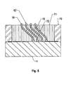
- the substrate (11) is positioned over the container (60) of liquid protective material (61) with the ball shaped contacts (16) submersed in the liquid (61). After the probe tips (16) are covered with the protective material (62), the substrate (11) is repositioned and a temporary dam (70) is placed around the array of probe wires (15) as shown in FIGURE 5.
- the cavity formed by the temporary dam (70) is filled with a liquid polymer material (71) that produces a thin coating of polymer (72) on the probe wires (15).
- the process is controlled to create a conformal, uniform thickness of the polymer material such as paralyne (72) on each of the probe wires (15) and the first surface (12) of the substrate (11) between the probe wires (15).
- the probe structure (10) after depositing the protective coating (62) on the ends of wires (15) can be emersed into a solution while an electric potential is applied to the wires (15) to electrolytically deposit a polymer such as a polyimide onto the surface of the wires (15).
- Useful processes are described in U.S. Patent 5,152,880 and U.S. Patent No's. 5,021,129, 5,242,713 and 5,242,551.
- FIGURE 6 shows the process step for adding the electrically conductive layer (90) on the surface of the polymer material (72).
- the conductive layer (90) can be added by electroless plating, electrophoretic plating, sputtering, or evaporation processes using palladium, chrome, copper, or other conductive materials.
- Conductive polymers can also be used as the ground layer (90) on the surface of the insulating polymer material (72).
- the protective coating (62) on the probe tips (16) is removed to expose the ball shaped contacts (16).
- Coating (62) can be a water soluble wax or other wax which can be later removed by commonly known techniques.
- electrically conductive layer (90) can be electrochemically deposited by the methods described in U.S. Patent 5,242,713.
- a halogenated polymer material such as perflorinated polymer, such as Teflon (Dupont Registered Trademark) is used as dielectric layer (70)
- an electrically conductive layer can be electrochemically disposed thereon according to the teaching of U.S. Patent 5,374,454.
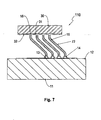
- FIGURE 7 shows a cross section of another embodiment of the high performance test probe (110).
- This embodiment (110) uses the same construction as the embodiment (10) of Figure 1 without the conductive layer (90) on the surface of the polymer material (72). While the electrical performance of this embodiment is not as good as the preferred embodiment, lower fabrication costs are the main advantage.
- the coating (72) can also be a material with high elasticity such as a stiff metal such as Invar, Cu/Invar/Cu, nickel which will enhance the flexibility of the elongated conductor (15).
- FIGURE 8 shows a cross section of another embodiment of the high performance test probe (120).
- This embodiment uses a thin sheet (81) (preferably Invar) to control the accuracy of the probe tip (16) positions.
- Sheet (81) can be any material such as a metal, a polymer, a glass and a ceramic.
- Invar is chosen to provide a TCE that is closely matched to the TCE of the silicon wafer IC (30) to be tested. Other materials with a TCE in the range of 2 to 8 ppm can also be used for the surface layer (81).
- a plurality of holes (82) are formed in the thin sheet (81) and are aligned with the corresponding probe tips (16).
- the thin Invar sheet (81) is supported by an elastomer frame (80) surrounding the array of probes.
- the thin invar sheet (81) can also be coated or laminated with a thin layer of polymer material on both the top and bottom sides to insulate the sheet (81) from the probe tip (16).
- FIGURE 9 shows a cross section of another embodiment of the high performance test probe (130).
- This embodiment is similar to the embodiment of Figure 7 in that it uses a thin Invar sheet (81) to control the accuracy of the probe tip (16) positions.
- This embodiment also uses a compliant conductive polymer (83), such as conductive siloxane or a conductive foam elastomer, to fill the cavity between the probe wires (15) that is formed by the elastomer frame (80) and the thin sheet (81).
- the compliant conductive polymer (83) is in contact with a ground terminal (92) on the first surface (12) of the substrate (11) and provides a ground shield for each of the probe wires (15). Electrically conductive polymers are described in U.S. Patent 5,198,153.
- FIGURE 13 a structure such as shown in FIGURE 3 is immersed in a tank (1302) containing an electrolytic solution (1304) such as described in U.S. Patent 5,152,880 to deposit a polyimide from polyimide solution or a polyimide from a polyisomide as described in U.S. Patent No's. 5,021,129, 5,242,713 and 5,242,551, the teachings of which are incorporated herein by reference.
- the appropriate currents and biases are applied to the wires (15) by applying the currents and voltages to contact pads such as contact pads (1317) which are electrically connected to each of the wires (15) to result in a polymer coating 1402 of FIGURE 14.
- the structure 1404 of FIGURE 14 with polymer coated wires (1406) can then be immersed in an electrolytic solution such as described in U.S. Patent 5,242,713 to deposit a metal coating such as a copper coating on the polymer coating 1402.
- an electrolytic solution such as described in U.S. Patent 5,242,713
- a metal coating such as a copper coating on the polymer coating 1402.
- This can be achieved by replacing solution 1304 in FIGURE 14 with the solution of U.S. Patent 5,242,713 and applying the appropriate bias and current to contact 1317 to result in the structure of FIGURE 15 with dielectric coating 1404 coated with electrical conductor 1502.
- protective layer 62 can be removed as described above to result in the structure of FIGURE 16.
- the space between the elongated conductors can be filled with a material (1704).
- the material can be an electrically conductive polymer which provides a common electrical connection between electrically conductive layer (1502) on elongated conductors 15.
- the material 1704 can be electrically contacted by contact pad (1702).
- material 1704 can be a dielectric material filled with electrically conductive particles 1706 such as metal particles.
- material (1704) can be a blend of a dielectric polymer and an electrically conductive polymer.
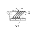
- a sheet (1808) such as (81) of FIGURE 9 can be disposed over the ends of the coaxial elongated conductor as shown in FIGURE 18.
- Sheet (1808) can be an electrical conductor or a multilayer sheet having a dielectric and electrical conductor layer.
- Sheet (1802) can be bonded to outer conductor (1502) with an electrically conductive adhesive or solder bond at location (1804) to form a common electrical connection between the outer conductors (1402) of each coaxial elongated conductor (1806). Electrical contact can be made to sheet (1802) such as at 1810 to hold it at a fixed potential as described in the references incorporated herein by reference below.
- Substrate (11) can be designed so that electrically conductive pads (21) on surface (19) are electrically connected to elongated conductors (15) to thereby provide a bias for the electrochemical processes.
- FIGURE 15 of the electrochemical deposition of electrically conductive layer 1502 is allowed to proceed long enough and if the electrically conductive pads (1902) shown in FIGURE 19 are close enough the electrically conductive layers (1502) on adjacent elongated conductors (15) will bridge the gap between pads (1502) and merge as shown at location (1704) to form a common outer electrical conductor which can be biased to a common potential as shown at location (1906).
- protection layer (62) can be eliminated. If the center elongated conductor (15) is completely immersed in the solution of Figure 13, the conductor (15) will be completely coated with dielectric layer (1406) and electrically conductive layer (1502).
- the coated ends of elongated conductor (15) are dipped into etchants to remove the layers 1402 and 1502 at the ends to result in the structure of FIGURE 17.
- a laser can be used to bum off or volatilize the layers 1402 and 1502 at the ends of elongated conductors 15. Alternatively, these layers can be abraded away.
- FIGURE 17 schematically shows an apparatus for moving probe structure 10 towards and away from electronic device 204 so that probe tips 210 engage and disengage electrical contact locations 212 on electronic device 204.
- Probe 20 is mounted on to holder 200 having means 214 for applying electric power to the probe tips 210.
- Electronic device 206 is held on base 206.
- Holder 200 is physically connected to support 202 which is converted to arm 208 which is converted to base 206.
- Support 202 is adapted for use and down movement. Examples of an apparatus to provide the means for support and up and down movement can be found in U.S. Patent 5,439,161 and U.S. Patent 5,132,613, the teachings of which are incorporated herein by reference.
- electrically conductive polymers can be combined with elastomeric materials to form elastomeric electrically conductive polymeric materials.
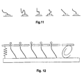
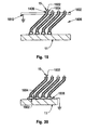
- the probe wire can be angled, curved, or straight and the probe tip can be ball shaped, straight, or flattened.
Landscapes
- Physics & Mathematics (AREA)
- General Physics & Mathematics (AREA)
- Geometry (AREA)
- Measuring Leads Or Probes (AREA)
- Testing Or Measuring Of Semiconductors Or The Like (AREA)
Description
U.S. Patent 5,371,654 entitled, "THREE DIMENSIONAL HIGH PERFORMANCE INTERCONNECTION PACKAGE";
U.S. Patent Application Serial No. 08/614,417 entitled, "HIGH DENSITY CANTILEVERED PROBE FOR ELECTRONIC DEVICES";
U.S. Patent Application Serial No. 08/641,667 entitled, "HIGH DENSITY TEST PROBE WITH RIGID SURFACE STRUCTURE";
U.S. Patent Application Serial No. 08/527,733 entitled, "INTERCONNECTOR WITH CONTACT PADS HAVING ENHANCED DURABILITY";
U.S. Patent Application Serial No. 08/752,469 entitled, "FOAMED ELASTOMERS FOR WAFER PROBING APPLICATIONS AND INTERPOSER CONNECTORS";
U.S. Patent Application Serial No. 08/744,903 entitled, "INTEGRAL RIGID CHIP TEST PROBE";
U.S. Patent Application Serial No. 08/756,831 entitled, "HIGH TEMPERATURE CHIP TEST PROBE";
U.S. Patent Application Serial No. 08/756,830 entitled, "A HIGH DENSITY INTEGRAL TEST PROBE AND FABRICATION METHOD";
U.S. Patent Application Serial No. 08/754,869 entitled, "HIGH DENSITY INTEGRATED CIRCUIT APPARATUS, TEST PROBE AND METHODS OF USE THEREOF".
Claims (9)
- A probe structure (10) comprising:a substrate (11) having a surface (12);a plurality of elongated electrical conductors (15) extending away from said surface;each of said elongated electrical conductors having a dielectric coating (72); andeach of said elongated electrical conductors having a first end (14) affixed to said surface and a second end (16) projecting away from said surface;a coating of an electrically conductive material (90) disposed on said dielectric coating; and characterised in that the structure further comprises an electrically conductive coating disposed on said surface (12) electrically interconnecting said surface (12) and said electrical conductors (15), wherein said electrically conductive coating is disposed on said surface (12) at locations other than the locations of the stems (14) of the conductors (15).
- A structure according to claim 1 wherein said elongated electrical conductors have ends which are not coated with said dielectric coating.
- A structure according to claim 1 wherein said electrically conductive coating on said plurality of elongated conductors and electrical coating on said surface are a substantially continuous coating.
- A structure according to claim 1 further including a means for maintaining said plurality of said second ends in substantially fixed positions with respect to a reference position.
- A structure according to claim 1 wherein said first end is affixed to said surface at an electrical contact location.
- A structure according to claim 4 wherein said means for maintaining is a sheet or material having a plurality of openings therein through which said second ends project.
- A structure according to claim 6 wherein said sheet comprises a sheet of electrically conductive material having a plurality of first through holes therein, and a sheet of dielectric material having a plurality of second through holes therein, said firs through holes have a smaller diameter than said second through holes to provide a means for preventing said elongated electrical conductors from electrically contacting said sheet of electrically conductive material.
- A structure according to claim 7 wherein sheet or electrically conductive material has a first side and a second side, said sheet of dielectric material is disposed on either of said first side and said second side of said sheet of electrically conductive material.
- A structure according to claim 7 where there is disposed on said first side and said second side of said sheet of electrically conductive material a layer of said dielectric material.
Applications Claiming Priority (3)
| Application Number | Priority Date | Filing Date | Title |
|---|---|---|---|
| US2605096P | 1996-09-13 | 1996-09-13 | |
| US26050P | 1996-09-13 | ||
| PCT/US1997/013698 WO1998011445A1 (en) | 1996-09-13 | 1997-09-12 | Probe structure having a plurality of discrete insulated probe tips |
Publications (2)
| Publication Number | Publication Date |
|---|---|
| EP0925509A1 EP0925509A1 (en) | 1999-06-30 |
| EP0925509B1 true EP0925509B1 (en) | 2005-09-07 |
Family
ID=21829590
Family Applications (1)
| Application Number | Title | Priority Date | Filing Date |
|---|---|---|---|
| EP97942379A Expired - Lifetime EP0925509B1 (en) | 1996-09-13 | 1997-09-12 | Probe structure having a plurality of discrete insulated probe tips |
Country Status (5)
| Country | Link |
|---|---|
| US (3) | US6452406B1 (en) |
| EP (1) | EP0925509B1 (en) |
| JP (1) | JP2000502810A (en) |
| DE (1) | DE69734158T2 (en) |
| WO (1) | WO1998011445A1 (en) |
Families Citing this family (48)
| Publication number | Priority date | Publication date | Assignee | Title |
|---|---|---|---|---|
| US7368924B2 (en) * | 1993-04-30 | 2008-05-06 | International Business Machines Corporation | Probe structure having a plurality of discrete insulated probe tips projecting from a support surface, apparatus for use thereof and methods of fabrication thereof |
| US20020004320A1 (en) * | 1995-05-26 | 2002-01-10 | David V. Pedersen | Attaratus for socketably receiving interconnection elements of an electronic component |
| US5914613A (en) | 1996-08-08 | 1999-06-22 | Cascade Microtech, Inc. | Membrane probing system with local contact scrub |
| US7063541B2 (en) * | 1997-03-17 | 2006-06-20 | Formfactor, Inc. | Composite microelectronic spring structure and method for making same |
| US6256882B1 (en) | 1998-07-14 | 2001-07-10 | Cascade Microtech, Inc. | Membrane probing system |
| DE10143173A1 (en) | 2000-12-04 | 2002-06-06 | Cascade Microtech Inc | Wafer probe has contact finger array with impedance matching network suitable for wide band |
| JP2002343478A (en) * | 2001-05-16 | 2002-11-29 | Tyco Electronics Amp Kk | Electrical contact and electrical connection member using the same |
| US6781390B2 (en) * | 2001-07-20 | 2004-08-24 | Nhk Spring Co., Ltd. | Conductive coil contact member |
| WO2003052435A1 (en) | 2001-08-21 | 2003-06-26 | Cascade Microtech, Inc. | Membrane probing system |
| EP1438591A1 (en) * | 2001-10-10 | 2004-07-21 | Delaware Capital Formation, Inc. | Coaxial tilt pin fixture for testing high frequency circuit boards |
| US7132736B2 (en) * | 2001-10-31 | 2006-11-07 | Georgia Tech Research Corporation | Devices having compliant wafer-level packages with pillars and methods of fabrication |
| JP4054208B2 (en) | 2002-04-01 | 2008-02-27 | 富士通株式会社 | Contactor manufacturing method |
| EP1509776A4 (en) * | 2002-05-23 | 2010-08-18 | Cascade Microtech Inc | Probe for testing a device under test |
| US7199305B2 (en) * | 2002-08-08 | 2007-04-03 | Nanoink, Inc. | Protosubstrates |
| US20040135594A1 (en) * | 2003-01-14 | 2004-07-15 | Beaman Brian Samuel | Compliant interposer assembly for wafer test and "burn-in" operations |
| JP2004265729A (en) * | 2003-02-28 | 2004-09-24 | Jst Mfg Co Ltd | Anisotropic conductive sheet |
| US7057404B2 (en) | 2003-05-23 | 2006-06-06 | Sharp Laboratories Of America, Inc. | Shielded probe for testing a device under test |
| US20040249825A1 (en) * | 2003-06-05 | 2004-12-09 | International Business Machines Corporation | Administering devices with dynamic action lists |
| DE202004021093U1 (en) | 2003-12-24 | 2006-09-28 | Cascade Microtech, Inc., Beaverton | Differential probe for e.g. integrated circuit, has elongate probing units interconnected to respective active circuits that are interconnected to substrate by respective pair of flexible interconnects |
| US7172431B2 (en) * | 2004-08-27 | 2007-02-06 | International Business Machines Corporation | Electrical connector design and contact geometry and method of use thereof and methods of fabrication thereof |
| WO2006031280A2 (en) * | 2004-09-13 | 2006-03-23 | Microfabrica Inc. | Probe arrays and method for making |
| DE202005021435U1 (en) | 2004-09-13 | 2008-02-28 | Cascade Microtech, Inc., Beaverton | Double-sided test setups |
| US7771803B2 (en) | 2004-10-27 | 2010-08-10 | Palo Alto Research Center Incorporated | Oblique parts or surfaces |
| EP1834379B1 (en) * | 2004-12-16 | 2012-07-11 | International Business Machines Corporation | Metalized elastomeric electrical contacts |
| US7771208B2 (en) | 2004-12-16 | 2010-08-10 | International Business Machines Corporation | Metalized elastomeric electrical contacts |
| US7535247B2 (en) | 2005-01-31 | 2009-05-19 | Cascade Microtech, Inc. | Interface for testing semiconductors |
| US7656172B2 (en) | 2005-01-31 | 2010-02-02 | Cascade Microtech, Inc. | System for testing semiconductors |
| US20060267605A1 (en) * | 2005-05-27 | 2006-11-30 | Yang Kei-Wean C | Differential measurement probe having a ground clip system for the probing tips |
| US7721430B2 (en) * | 2006-02-22 | 2010-05-25 | Sv Probe Pte Ltd. | Approach for fabricating cantilever probes |
| US7764072B2 (en) | 2006-06-12 | 2010-07-27 | Cascade Microtech, Inc. | Differential signal probing system |
| US7723999B2 (en) | 2006-06-12 | 2010-05-25 | Cascade Microtech, Inc. | Calibration structures for differential signal probing |
| US7403028B2 (en) | 2006-06-12 | 2008-07-22 | Cascade Microtech, Inc. | Test structure and probe for differential signals |
| US7338300B1 (en) * | 2006-11-28 | 2008-03-04 | Inventec Corporation | Static electricity conductive mechanism |
| US8832936B2 (en) * | 2007-04-30 | 2014-09-16 | International Business Machines Corporation | Method of forming metallized elastomeric electrical contacts |
| US7876114B2 (en) | 2007-08-08 | 2011-01-25 | Cascade Microtech, Inc. | Differential waveguide probe |
| US7888957B2 (en) | 2008-10-06 | 2011-02-15 | Cascade Microtech, Inc. | Probing apparatus with impedance optimized interface |
| US8410806B2 (en) | 2008-11-21 | 2013-04-02 | Cascade Microtech, Inc. | Replaceable coupon for a probing apparatus |
| JP5683943B2 (en) * | 2010-12-27 | 2015-03-11 | 三菱電線工業株式会社 | PROBE PIN AND PROBE PIN MANUFACTURING METHOD |
| KR101284362B1 (en) * | 2011-05-30 | 2013-07-08 | 주식회사 코엠테크 | Inspection jig and method of producing the same |
| US10177054B2 (en) * | 2011-10-27 | 2019-01-08 | Global Circuit Innovations, Inc. | Method for remapping a packaged extracted die |
| US9059545B2 (en) * | 2012-07-11 | 2015-06-16 | Tyco Electronics Corporations | Socket connectors and methods of assembling socket connectors |
| TWI472772B (en) * | 2013-01-11 | 2015-02-11 | Mpi Corp | Probe, probe card and manufacturing method thereof |
| CN107257928B (en) * | 2014-12-30 | 2020-12-01 | 泰克诺探头公司 | Contact probe for a test head |
| JP6569377B2 (en) * | 2015-08-14 | 2019-09-04 | 富士通株式会社 | Cable connector and wiring board |
| TWI642940B (en) * | 2017-09-01 | 2018-12-01 | 中華精測科技股份有限公司 | Probe assembly and probe structure thereof |
| JP7254450B2 (en) * | 2018-05-16 | 2023-04-10 | 日本電産リード株式会社 | Probe, inspection jig, inspection apparatus, and probe manufacturing method |
| TWI680300B (en) * | 2019-03-18 | 2019-12-21 | 中華精測科技股份有限公司 | Probe card device and conductive probe thereof |
| US20220178969A1 (en) * | 2020-12-03 | 2022-06-09 | Star Technologies, Inc. | Probe device and method of assembling the same |
Family Cites Families (34)
| Publication number | Priority date | Publication date | Assignee | Title |
|---|---|---|---|---|
| US3878145A (en) * | 1965-03-13 | 1975-04-15 | Reichhold Albert Chemie Ag | Process for producing water-dilutable coating compositions suitable for electrocoating |
| US3669850A (en) * | 1969-07-18 | 1972-06-13 | Cedo Draca | Method for the production of abrasive brushing elements |
| NL7316245A (en) * | 1973-10-04 | 1975-04-08 | Galentan Ag | METHOD FOR SELECTIVELY APPLYING A COATING ON THE METAL PARTS OF ELECTRICAL CONSTRUCTION ELEMENTS PROVIDED BY AN INSULATING BODY. |
| GB1477060A (en) * | 1974-06-05 | 1977-06-22 | Mitsubishi Electric Corp | Process for preparing insulation coated wire by electrode position |
| US4312716A (en) * | 1980-11-21 | 1982-01-26 | Western Electric Co., Inc. | Supporting an array of elongate articles |
| JPS58165056A (en) | 1982-03-25 | 1983-09-30 | Nippon Denshi Zairyo Kk | Probe card |
| US5917707A (en) | 1993-11-16 | 1999-06-29 | Formfactor, Inc. | Flexible contact structure with an electrically conductive shell |
| US5476211A (en) * | 1993-11-16 | 1995-12-19 | Form Factor, Inc. | Method of manufacturing electrical contacts, using a sacrificial member |
| US4739259A (en) * | 1986-08-01 | 1988-04-19 | Tektronix, Inc. | Telescoping pin probe |
| US5103557A (en) * | 1988-05-16 | 1992-04-14 | Leedy Glenn J | Making and testing an integrated circuit using high density probe points |
| US5233011A (en) * | 1988-10-20 | 1993-08-03 | Mitsui Toatsu Chemicals, Incorporated | Process for preparing insulated wire |
| JP2903652B2 (en) | 1990-06-19 | 1999-06-07 | 富士ゼロックス株式会社 | Facsimile control method |
| JPH04240570A (en) | 1991-01-24 | 1992-08-27 | Shimadzu Corp | Micro-probe board |
| US5104494A (en) * | 1991-07-02 | 1992-04-14 | Rockwell International Corp. | Method of restoring solderability |
| JPH0555319A (en) | 1991-08-26 | 1993-03-05 | Nec Ibaraki Ltd | Socket for ic |
| US5225777A (en) | 1992-02-04 | 1993-07-06 | International Business Machines Corporation | High density probe |
| US5371654A (en) | 1992-10-19 | 1994-12-06 | International Business Machines Corporation | Three dimensional high performance interconnection package |
| US5532613A (en) * | 1993-04-16 | 1996-07-02 | Tokyo Electron Kabushiki Kaisha | Probe needle |
| JP3100097B2 (en) | 1993-04-16 | 2000-10-16 | 東京エレクトロン株式会社 | Contactor for prober |
| KR0138618B1 (en) * | 1993-08-04 | 1998-06-15 | 이노우에 아끼라 | Vertical probe tester card with coaxial probes |
| US5483741A (en) | 1993-09-03 | 1996-01-16 | Micron Technology, Inc. | Method for fabricating a self limiting silicon based interconnect for testing bare semiconductor dice |
| US5806181A (en) * | 1993-11-16 | 1998-09-15 | Formfactor, Inc. | Contact carriers (tiles) for populating larger substrates with spring contacts |
| US6336269B1 (en) * | 1993-11-16 | 2002-01-08 | Benjamin N. Eldridge | Method of fabricating an interconnection element |
| US5534784A (en) | 1994-05-02 | 1996-07-09 | Motorola, Inc. | Method for probing a semiconductor wafer |
| JPH07321490A (en) | 1994-05-26 | 1995-12-08 | Shinano Polymer Kk | Electric connector |
| US5495667A (en) | 1994-11-07 | 1996-03-05 | Micron Technology, Inc. | Method for forming contact pins for semiconductor dice and interconnects |
| AU4283996A (en) | 1994-11-15 | 1996-06-19 | Formfactor, Inc. | Electrical contact structures from flexible wire |
| KR100375177B1 (en) * | 1995-05-19 | 2003-05-09 | 마츠시타 덴끼 산교 가부시키가이샤 | Method of inspecting semiconductor device |
| JP3001182B2 (en) | 1995-08-29 | 2000-01-24 | 信越ポリマー株式会社 | Liquid crystal panel inspection apparatus and method of manufacturing the same |
| JP3307823B2 (en) | 1996-02-23 | 2002-07-24 | 松下電器産業株式会社 | Manufacturing method of contact parts for electronic component inspection |
| JPH09281145A (en) | 1996-04-15 | 1997-10-31 | Toppan Printing Co Ltd | Inspecting jig with anisotropic conductive material and its manufacture |
| JPH09304472A (en) | 1996-05-10 | 1997-11-28 | Hitachi Ltd | Connecting device |
| JP3128199B2 (en) | 1996-06-28 | 2001-01-29 | 信越ポリマー株式会社 | Inspection probe |
| US6592738B2 (en) * | 1997-01-31 | 2003-07-15 | Elisha Holding Llc | Electrolytic process for treating a conductive surface and products formed thereby |
-
1997
- 1997-09-12 WO PCT/US1997/013698 patent/WO1998011445A1/en active IP Right Grant
- 1997-09-12 US US09/254,798 patent/US6452406B1/en not_active Expired - Lifetime
- 1997-09-12 JP JP10513644A patent/JP2000502810A/en active Pending
- 1997-09-12 EP EP97942379A patent/EP0925509B1/en not_active Expired - Lifetime
- 1997-09-12 DE DE69734158T patent/DE69734158T2/en not_active Expired - Lifetime
-
2002
- 2002-02-01 US US10/066,171 patent/US8486250B2/en not_active Expired - Fee Related
-
2009
- 2009-08-21 US US12/545,537 patent/US8491772B2/en not_active Expired - Fee Related
Also Published As
| Publication number | Publication date |
|---|---|
| US6452406B1 (en) | 2002-09-17 |
| US20090308756A1 (en) | 2009-12-17 |
| US8491772B2 (en) | 2013-07-23 |
| EP0925509A1 (en) | 1999-06-30 |
| US8486250B2 (en) | 2013-07-16 |
| DE69734158D1 (en) | 2005-10-13 |
| JP2000502810A (en) | 2000-03-07 |
| DE69734158T2 (en) | 2006-06-22 |
| US20020089344A1 (en) | 2002-07-11 |
| WO1998011445A1 (en) | 1998-03-19 |
Similar Documents
| Publication | Publication Date | Title |
|---|---|---|
| EP0925509B1 (en) | Probe structure having a plurality of discrete insulated probe tips | |
| US9404942B2 (en) | Coaxial probe structure of elongated electrical conductors projecting from a support structure | |
| EP0925510B1 (en) | Integrated compliant probe for wafer level test and burn-in | |
| US5785538A (en) | High density test probe with rigid surface structure | |
| KR100454546B1 (en) | Contact structure having silicon finger contactors and total stack-up structure using same | |
| US5811982A (en) | High density cantilevered probe for electronic devices | |
| US7332922B2 (en) | Method for fabricating a structure for making contact with a device | |
| US5914614A (en) | High density cantilevered probe for electronic devices | |
| US6329827B1 (en) | High density cantilevered probe for electronic devices | |
| US6722032B2 (en) | Method of forming a structure for electronic devices contact locations | |
| US20050062492A1 (en) | High density integrated circuit apparatus, test probe and methods of use thereof | |
| US6534710B2 (en) | Packaging and interconnection of contact structure | |
| US6525551B1 (en) | Probe structures for testing electrical interconnections to integrated circuit electronic devices | |
| EP0925513B1 (en) | Wafer scale high density probe assembly, apparatus for use thereof and methods of fabrication thereof | |
| US7282945B1 (en) | Wafer scale high density probe assembly, apparatus for use thereof and methods of fabrication thereof | |
| KR20010076322A (en) | Contact structure having contact bumps |
Legal Events
| Date | Code | Title | Description |
|---|---|---|---|
| PUAI | Public reference made under article 153(3) epc to a published international application that has entered the european phase |
Free format text: ORIGINAL CODE: 0009012 |
|
| 17P | Request for examination filed |
Effective date: 19990329 |
|
| AK | Designated contracting states |
Kind code of ref document: A1 Designated state(s): DE FR GB |
|
| 17Q | First examination report despatched |
Effective date: 20040629 |
|
| GRAP | Despatch of communication of intention to grant a patent |
Free format text: ORIGINAL CODE: EPIDOSNIGR1 |
|
| GRAS | Grant fee paid |
Free format text: ORIGINAL CODE: EPIDOSNIGR3 |
|
| GRAA | (expected) grant |
Free format text: ORIGINAL CODE: 0009210 |
|
| AK | Designated contracting states |
Kind code of ref document: B1 Designated state(s): DE FR GB |
|
| REG | Reference to a national code |
Ref country code: GB Ref legal event code: FG4D |
|
| REF | Corresponds to: |
Ref document number: 69734158 Country of ref document: DE Date of ref document: 20051013 Kind code of ref document: P |
|
| ET | Fr: translation filed | ||
| PLBE | No opposition filed within time limit |
Free format text: ORIGINAL CODE: 0009261 |
|
| STAA | Information on the status of an ep patent application or granted ep patent |
Free format text: STATUS: NO OPPOSITION FILED WITHIN TIME LIMIT |
|
| 26N | No opposition filed |
Effective date: 20060608 |
|
| PGFP | Annual fee paid to national office [announced via postgrant information from national office to epo] |
Ref country code: FR Payment date: 20121001 Year of fee payment: 16 |
|
| REG | Reference to a national code |
Ref country code: FR Ref legal event code: ST Effective date: 20140530 |
|
| PG25 | Lapsed in a contracting state [announced via postgrant information from national office to epo] |
Ref country code: FR Free format text: LAPSE BECAUSE OF NON-PAYMENT OF DUE FEES Effective date: 20130930 |
|
| PGFP | Annual fee paid to national office [announced via postgrant information from national office to epo] |
Ref country code: GB Payment date: 20150909 Year of fee payment: 19 |
|
| REG | Reference to a national code |
Ref country code: DE Ref legal event code: R081 Ref document number: 69734158 Country of ref document: DE Owner name: GLOBALFOUNDRIES INC., KY Free format text: FORMER OWNER: INTERNATIONAL BUSINESS MACHINES CORPORATION, ARMONK, NY, US Ref country code: DE Ref legal event code: R082 Ref document number: 69734158 Country of ref document: DE Representative=s name: RICHARDT PATENTANWAELTE PARTG MBB, DE Ref country code: DE Ref legal event code: R081 Ref document number: 69734158 Country of ref document: DE Owner name: GLOBALFOUNDRIES INC., KY Free format text: FORMER OWNER: INTERNATIONAL BUSINESS MACHINES CORPORATION, ARMONK, N.Y., US |
|
| REG | Reference to a national code |
Ref country code: DE Ref legal event code: R082 Ref document number: 69734158 Country of ref document: DE Representative=s name: RICHARDT PATENTANWAELTE PARTG MBB, DE Ref country code: DE Ref legal event code: R081 Ref document number: 69734158 Country of ref document: DE Owner name: GLOBALFOUNDRIES INC., KY Free format text: FORMER OWNER: GLOBALFOUNDRIES US 2 LLC (N.D.GES.DES STAATES DELAWARE), HOPEWELL JUNCTION, N.Y., US |
|
| REG | Reference to a national code |
Ref country code: FR Ref legal event code: TP Owner name: GLOBALFOUNDRIES INC., GB Effective date: 20160829 |
|
| PGFP | Annual fee paid to national office [announced via postgrant information from national office to epo] |
Ref country code: DE Payment date: 20160907 Year of fee payment: 20 |
|
| GBPC | Gb: european patent ceased through non-payment of renewal fee |
Effective date: 20160912 |
|
| PG25 | Lapsed in a contracting state [announced via postgrant information from national office to epo] |
Ref country code: GB Free format text: LAPSE BECAUSE OF NON-PAYMENT OF DUE FEES Effective date: 20160912 |
|
| REG | Reference to a national code |
Ref country code: DE Ref legal event code: R071 Ref document number: 69734158 Country of ref document: DE |