EP0813313A2 - Dispositif de réception pour communication mobile - Google Patents
Dispositif de réception pour communication mobile Download PDFInfo
- Publication number
- EP0813313A2 EP0813313A2 EP19970109677 EP97109677A EP0813313A2 EP 0813313 A2 EP0813313 A2 EP 0813313A2 EP 19970109677 EP19970109677 EP 19970109677 EP 97109677 A EP97109677 A EP 97109677A EP 0813313 A2 EP0813313 A2 EP 0813313A2
- Authority
- EP
- European Patent Office
- Prior art keywords
- code
- output
- value
- phase
- integrator
- Prior art date
- Legal status (The legal status is an assumption and is not a legal conclusion. Google has not performed a legal analysis and makes no representation as to the accuracy of the status listed.)
- Granted
Links
Images


Classifications
-
- H—ELECTRICITY
- H04—ELECTRIC COMMUNICATION TECHNIQUE
- H04J—MULTIPLEX COMMUNICATION
- H04J13/00—Code division multiplex systems
- H04J13/10—Code generation
-
- H—ELECTRICITY
- H04—ELECTRIC COMMUNICATION TECHNIQUE
- H04B—TRANSMISSION
- H04B1/00—Details of transmission systems, not covered by a single one of groups H04B3/00 - H04B13/00; Details of transmission systems not characterised by the medium used for transmission
- H04B1/69—Spread spectrum techniques
- H04B1/707—Spread spectrum techniques using direct sequence modulation
- H04B1/7073—Synchronisation aspects
-
- H—ELECTRICITY
- H04—ELECTRIC COMMUNICATION TECHNIQUE
- H04B—TRANSMISSION
- H04B1/00—Details of transmission systems, not covered by a single one of groups H04B3/00 - H04B13/00; Details of transmission systems not characterised by the medium used for transmission
- H04B1/69—Spread spectrum techniques
- H04B1/707—Spread spectrum techniques using direct sequence modulation
- H04B1/7097—Interference-related aspects
- H04B1/711—Interference-related aspects the interference being multi-path interference
- H04B1/7115—Constructive combining of multi-path signals, i.e. RAKE receivers
- H04B1/7117—Selection, re-selection, allocation or re-allocation of paths to fingers, e.g. timing offset control of allocated fingers
-
- H—ELECTRICITY
- H04—ELECTRIC COMMUNICATION TECHNIQUE
- H04B—TRANSMISSION
- H04B1/00—Details of transmission systems, not covered by a single one of groups H04B3/00 - H04B13/00; Details of transmission systems not characterised by the medium used for transmission
- H04B1/69—Spread spectrum techniques
- H04B1/707—Spread spectrum techniques using direct sequence modulation
- H04B1/7097—Interference-related aspects
- H04B1/711—Interference-related aspects the interference being multi-path interference
- H04B1/7115—Constructive combining of multi-path signals, i.e. RAKE receivers
- H04B1/712—Weighting of fingers for combining, e.g. amplitude control or phase rotation using an inner loop
-
- H—ELECTRICITY
- H04—ELECTRIC COMMUNICATION TECHNIQUE
- H04B—TRANSMISSION
- H04B1/00—Details of transmission systems, not covered by a single one of groups H04B3/00 - H04B13/00; Details of transmission systems not characterised by the medium used for transmission
- H04B1/69—Spread spectrum techniques
- H04B1/707—Spread spectrum techniques using direct sequence modulation
- H04B2001/70706—Spread spectrum techniques using direct sequence modulation using a code tracking loop, e.g. a delay locked loop
-
- H—ELECTRICITY
- H04—ELECTRIC COMMUNICATION TECHNIQUE
- H04B—TRANSMISSION
- H04B2201/00—Indexing scheme relating to details of transmission systems not covered by a single group of H04B3/00 - H04B13/00
- H04B2201/69—Orthogonal indexing scheme relating to spread spectrum techniques in general
- H04B2201/707—Orthogonal indexing scheme relating to spread spectrum techniques in general relating to direct sequence modulation
- H04B2201/70707—Efficiency-related aspects
- H04B2201/70709—Efficiency-related aspects with discontinuous detection
Definitions
- the present invention relates to a mobile communication receiving apparatus for spread spectrum (SS) communication used for code division multiple access (CDMA) communication or radio local area network (radio LAN) communication in a mobile communication field, and in particular to reduction in power consumption and enlargement of the synchronization acquisition and hunt range.
- SS spread spectrum
- CDMA code division multiple access
- radio LAN radio local area network
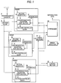
- a conventional mobile communication receiver for SS communication comprises a reception antenna 1 for receiving signals, high-frequency circuitry 2 made up of a signal amplifier (referred to simply “amplifier"), a frequency convertor, and a band-pass filter (BPF), a low-pass filter (LPF) 3 for limiting reception signals to a base band, three inverse spread modulation and data demodulation sections, which will be hereinafter referred to as fingers, 4, 9, and 14 for inversely spread modulating reception signals spread modulated at transmitting side and reproducing modulation data components, and a synthesizer 20 for synthesizing output signals of the fingers for amplifying the data signal strength, as shown in Figure 6.
- signal amplifier referred to simply "amplifier”
- BPF band-pass filter
- LPF low-pass filter
- synthesizer 20 for synthesizing output signals of the fingers for amplifying the data signal strength, as shown in Figure 6.
- Each of the fingers 4, 9, and 14 is made up of a PN code generation section 5, 10, 15 for generating the same pseudonoise (PN) code sequence as a transmitter, a synchronization acquisition/hunt section 6, 11, 16 for executing inverse spread modulation while synchronizing with the timing of a PN code of a reception signal and hunting the timing, an integrator 8, 13, 18 for integrating an inversely spread modulated reception signal for a given time for reproducing data, and a VCC section 7, 12, 17 for generating a voltage-controlled clock (VCC) used as a clock of the PN code generation section 5, 10, 15.
- PN code generation section 5, 10, 15 for generating the same pseudonoise (PN) code sequence as a transmitter
- PN pseudonoise
- a synchronization acquisition/hunt section 6, 11, 16 for executing inverse spread modulation while synchronizing with the timing of a PN code of a reception signal and hunting the timing
- an integrator 8, 13, 18 for integrating an inversely spread modulated reception signal for a given time
- the PN code generation sections 5, 10, and 15 are of the same configuration and perform the same operation; the integrators 8, 13, and 18 are of the same configuration and perform the same operation; and the VCC sections 7, 12, and 17 are of the same configuration and perform the same operation.
- the synchronization acquisition/hunt sections 6, 11, and 16 are of the same configuration, but execute inverse spread modulation at different timings.
- the fingers execute inverse spread modulation at different timings for reproducing data and the synthesizer 20 synthesizes the reproduced data, whereby the receiver enables pass diversity for separating and synthesizing direct waves and multiple-reflected waves for reproducing data.
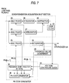
- FIG. 7 shows the configuration of the finger in more detail.
- the finger which has a delay lock loop (DLL) structure, comprises a multiplier 23 for multiplying PN code PN[k-1] leading inversely spread modulated PN code PN[k] by one chip in phase by a reception signal; a multiplier 24 for multiplying PN code PN[k+1] lagging PN[k] by one chip in phase by the reception signal, a multiplier 25 for multiplying PN[k] by the reception signal to output an inverse spread modulation output signal, an integrator 26 for integrating the output signals of the multiplier 23, an integrator 27 for integrating the output signals of the multiplier 24, a subtractor 48 for subtracting an output signal of the integrator 26 from an output signal of the integrator 27, a loop filter 29 for removing a noise component from an output component of the subtractor 48, an integrator 30 for integrating the output signals of the multiplier 25 and reproducing data, a threshold determiner 49 for comparing an output signal of the integrator 30 with a
- the PN code generator 35 has a function of making output lag behind or lead ahead by several chip intervals.
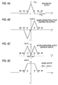
- Figure 4A shows the output of an integrator 30.
- the vertical axis is an auto-correlation function R(t) of a PN code sequence of a transmitter and a receiver and corresponds to the output of the integrator 30 in Figure 7.
- the horizontal axis shows PN code timing differences between the transmitter and receiver, wherein dt denotes one chip interval.
- R(t) indicates the maximum value; when the PN code timing difference is 1 chip or more, R(t) becomes 1/L (L: Integration number) and almost 0 because L is sufficiently large. Therefore, data demodulation is impossible in the receiver when PN code synchronization is not acquired.
- the receiver checks R(t) by the threshold determiner 49.
- R(t) is equal to or less than a threshold value
- the receiver makes the output PN code of the PN code generator 35 lag behind or lead ahead by several chip intervals for timing adjustment and again checks R(t).
- the receiver repeats this operation until the output of the integrator 30 exceeds the threshold value.
- the receiver fixes the timing for acquiring synchronization. This is the synchronization acquisition operation principle.
- Figure 4B shows an output characteristic of the subtractor 48 (D2(t)).
- Receiver PN codes used by the multipliers 23 and 24 (PN[k-1] and PN[k+1]) are 1-chip lead and lag signals ahead and behind PN code PN[k] used for inverse spread modulation in the multiplier 25. Therefore, the auto-correlation functions (outputs of the integrators 26 and 27) are provided by shifting R(t) in Figure 4A -dt and +dt and have the maximum values at -dt and +dt.
- the integrator 26 output is inverted and synthesized with the integrator 27 output by the subtractor 48, the output characteristic of the subtractor 48, D2(t), becomes as shown in Figure 4B. Therefore, D2(t) becomes an increasing function passing through the origin at the ⁇ dt interval.
- the phase of the VCC 33 is controlled by the signal resulting from removing the noise component of D2(t) through the loop filter 29, whereby the PN code of the reception signal can be hunted.
- the conventional mobile communication receiver having a plurality of fingers involves a problem of an increase in power consumption.
- the receiver for a mobile communication comprises: a power measurement unit for measuring power of reproduction output of the fingers and total power thereof, an error detection unit for detecting an error of output data of a synthesizer, and a control unit for controlling power on and off of the fingers based on the measurement result of the power measurement unit and the error detection result of the error detection unit.
- the fingers can be powered off in the range in which an error increase does not result for reducing power consumption.
- Each of the fingers comprises a first multiplier for multiplying a PN code (PN[k]) synchronized with a PN code of a transmitter by a base band reception signal, a second multiplier for multiplying a PN code (PN[k-1]) leading the PN[k] by one chip in phase by the base band reception signal, a third multiplier for multiplying a PN code (PN[k+1]) lagging the PN[k] by one chip in phase by the base band reception signal, an adder subtractor for performing addition and subtraction on integration values of outputs of the second and third multipliers, PN code supply means for changing phases of the PN codes generated by a PN code generator and supplying the resultant PN codes to the first, second, and third multipliers, and PN code control means for controlling the phase amount of the PN code changed by the PN code supply means based on the addition and subtraction result values of the adder subtractor and integration output of the first multiplier.
- the PN synchronization acquisition and hunt range for multiply
- a power measurement unit measures power of reproduction output of the fingers and total power thereof
- an error detection unit detects an error of output data of the synthesizer
- a control unit controls power on and off of the fingers based on the measurement result of the power measurement unit and the error detection result of the error detection unit. Power consumption can be reduced.
- control unit stores the total power Ps corresponding to reference error data from the relationship between the total power measured by the power measurement unit and the error detected by the error detection unit, and if the value resulting from subtracting Ps from the total power of reproduction output of the operating fingers is equal to or greater than the value resulting from adding the power of the finger having the minimum reproduction output power among the operating fingers and a constant d, which is a positive real number, powers off the finger having the minimum reproduction output power. While the total power more than the power Ps corresponding to the reference error data is always provided, the fingers can be powered off for reducing power consumption.
- each of the fingers has a first multiplier for multiplying a PN code (PN[k]) synchronized with a PN code of a transmitter by a base band reception signal, a first integrator for integrating output of the first multiplier, a second multiplier for multiplying a PN code (PN[k-1]) leading the PN[k] by one chip in phase by the base band reception signal, a second integrator for integrating output of the second multiplier, a third multiplier for multiplying a PN code (PN[k+1]) lagging the PN[k] by one chip in phase by the base band reception signal, a third integrator for integrating output of the third multiplier, an adder subtractor for performing addition and subtraction on outputs of the second and third integrators, a PN code generator for generating the same PN codes as the transmitter, a PN code supply unit for changing phases of the PN codes generated by the PN code generator and supplying the resultant PN codes to the first, second, and third multipliers,
- the PN code control unit is provided with a first comparator for comparing output of the first integrator with the addition result value of the adder subtractor in greater-than, equal-to, or less-than relation, a second comparator for comparing the subtraction result value of the adder subtractor with a numeric value 0 in greater-than, equal-to, or less-than relation, a third comparator for comparing a value ADD resulting from adding the addition result value of the adder subtractor to output of the first integrator with a numeric value 0 in greater-than, equal-to, or less-than relation and outputting 1 when ADD>0, otherwise 0, a phase shifter for outputting a phase amount control value to the PN code supply unit so as to shift the phase of the PN code supplied by the PN code supply unit by one chip every integration time when the third comparator outputs 0, and a phase hunter for selectively outputting a value 0, 1 or -1 added to the output value of the phase shifter based on outputs of the first and second compar
- the selection of the selector is controlled so that the shift amount of the feedback shift register is adjusted until the phase difference between the PN codes of the transmitter and receiver enters the synchronization acquisition range and that the synchronization can be hunted after it is acquired.
- a mobile communication receiver has a reception antenna 1; high-frequency circuitry 2; a low-pass filter (LPF) 3; three fingers 4, 9 and 14 each consisting of PN code generation sections 5, 10, 15, a synchronization acquisition/hunt section 6, 11, 16, a voltage-controlled clock (VCC) 7, 12, 17 and an integrator 8, 13, 18; a power measure 19 for measuring power of an output signal of each finger 4, 9, 14 and total power; a synthesizer 20 for synthesizing the output signals of the fingers; an error detector 21 for detecting an error of an output signal of the synthesizer 20; and a control section (central processing unit (CPU)) 22 for controlling power on and off of the fingers 4, 9, and 14 based on the measurement and detection results of the power measure 19 and the error detector 21.
- CPU central processing unit
- the reception antenna 1, the high-frequency circuity 2, and the LPF 3 have the same configuration as and perform the same operation as those of the conventional receiver in Figure 6.
- the finger 4 is made up of the PN code generation section 5, the synchronization acquisition/hunt section 6, the integrator 8, and the voltage-controlled clock (VCC) 7.
- the PN code generation section 5 outputs the same PN code as a transmitter at the same speed.
- the synchronization acquisition/hunt section 6 executes inverse spread modulation and outputs an inverse spread modulation output signal while synchronizing with the timing of a PN code of a reception signal and hunting the timing.
- the VCC 7 supplies a clock to the PN code generation section 5 and the phase of the clock is controlled by an output voltage of the synchronization acquisition/hunt section 6.
- the integrator 8 integrates inversely spread modulated reception signals output by the synchronization acquisition/hunt section 6 for a given time and reproduces data.
- the finger 9, 14 has the same configuration as the finger 4 and performs the same operation as the finger 4, but differs from the finger 4 in inverse spread modulation timing. Thus, bus diversity is enabled by outputs of the fingers 4, 9, and 14. Power on/off control of the fingers 4, 9, and 14 is performed by the CPU 22.
- the power measure 19 measures power (P1, P2, P3) of the output signal (reproduction data signal d4, d9, d14) of each of the fingers 4, 9, and 14 and total power (Pt), and transmits the measurement data to the CPU 22.
- the synthesizer 20 synthesizes d4, d9, and 14.
- the error detector 21 detects an error of the synthesizer 20 output signal, and transmits the error data (ED) to the CPU 22.
- the CPU 22 uses P1, P2, P3, Pt, and ED to perform power on/off control of the fingers 4, 9, and 14.
- FIG. 2 shows an on/off control procedure of the CPU 22.
- the CPU 22 first checks P1, P2, and P3. Next, it checks the relationship between Pt and ED, and stores the total power Ps of the power measure 19 when reproduction data output from the synthesizer 20 contains a maximum allowable error on performance. That is, the CPU 22 stores the signal power Ps of the power measure 19 corresponding to the ED reference value defining the maximum allowable error in the reproduction data.
- the receiver of the embodiment repeats the following operation:
- the signal power (Ps) corresponding to the reference error data (error data limit value which must be maintained at the minimum to hold the reception performance) is stored. If the difference between the total power of the finger outputs (Pt) and Ps is equal to or greater than the sum of the minimum power of the fingers and the positive constant d, the power of the finger outputting the minimum power is turned off. In this state, if the difference between the total power of the operating finger outputs (Pt) and Ps is equal to or greater than the sum of the minimum power of the operating fingers and the positive constant d, the power of the operating finger outputting the minimum power is turned off.
- the fingers having small output power among the operating fingers are turned off, when the total power (Pt) is equal to or greater than Ps by d or more, the fingers having small output power are turned off in sequence for saving power consumption.
- a whole mobile communication receiver of a second embodiment has the configuration in Figure 1, and each of fingers 4, 9, and 14 has the configuration shown in Figure 3.
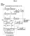
- the finger has a multiplier 23 for multiplying PN code PN[k-1] leading PN code PN[k] used for inverse spread modulation by one chip in phase by a reception signal, a multiplier 24 for multiplying PN code PN[k+1] lagging PN[k] by one chip in phase by the reception signal, a multiplier 25 for multiplying PN[k] by the reception signal to output an inverse spread modulation output signal, an integrator 26 for integrating the output signals of the multiplier 23, an integrator 27 for integrating the output signals of the multiplier 24, an adder subtractor 28 for performing addition and subtraction on an output signal of the integrator 26 and an output signal of the integrator 27, a loop filter 29 for removing a noise component of the subtraction result output from the adder subtractor 28, an integrator 30 for integrating the output signals of the multiplier 25 and reproducing data, a voltage-controlled clock (VCC) 33 whose phase is controlled by an output signal of the loop filter 29, a feedback shift register 34 of N taps for cyclically
- the multiplier 23 multiplies the PN code (PN[k-1]) leading the PN code (PN[k]) used for inverse spread modulation by one chip by a reception signal.
- the multiplier 24 multiplies the PN code (PN[k+1]) lagging PN[k] by one chip by the reception signal.
- the multiplier 25 multiplies PN[k] by the reception signal for inverse spread modulation.
- the integrators 26 and 27 integrate the output signals of the multipliers 23 and 24, respectively, for the same given time, and the adder subtractor 28 performs adding and substraction on the output signals of the integrators 26 and 27. To perform subtraction, the integrator 26 output signal is subtracted from the integrator 27 output signal. The substraction result signal is output to the loop filter 29 and the addition result signal and subtraction result signal are output to the PN code control section 31.
- the loop filter 29 removes noise of the subtraction result signal.
- the output signal from the loop filter 29 becomes D2(t) in Figure 4B. This signal controls the VCC 33 for hunting the phase of the PN code of the reception signal.
- the integrator 30 integrates the inversely spread modulated reception signal for the same time as the integration time of the integrator 26, 27 for reproducing data. This reproduction data is output to the synthesizer 20 and the power measure 19 in Figure 1.
- the PN code control section 31 uses the integrator 30 output signal and the adder subtractor 28 output signal to control the selector 32 and the feedback shift register 34, thereby enlarging the synchronization acquisition and hunt range, as described later.
- the PN code generator 35 calculates a PN code pattern from specific tap output of the feedback shift register 34, and generates the same PN code pattern as a transmitter.
- the feedback shift register 34 shifts the PN codes output from the PN code generator 35 by the VCC 33 clock. It is reset by the PN code control section 31, and restarts shifting the PN codes according to the shift count specified by the PN code control section 31.
- Each register output of the feedback shift register 34 is output to the selector 32. Then, the selector 32 selects one PN code (PN[k]) used for inverse spread modulation based on the signal of the PN code control section 31 from the register outputs of the feedback shift register 34, then, selects the register values preceding and following the selected PN code (PN[k-1] and PN[k+1]), and outputs the PN codes to the multipliers 25, 23 and 24.
- PN[k] PN code used for inverse spread modulation based on the signal of the PN code control section 31 from the register outputs of the feedback shift register 34, then, selects the register values preceding and following the selected PN code (PN[k-1] and PN[k+1]), and outputs the PN codes to the multipliers 25, 23 and 24.
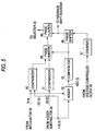
- the PN code control section 31 has a comparator 40 for comparing output of the integrator 30 with addition output of the adder subtractor 28, a comparator 41 for comparing substraction output of the adder subtractor 28 with threshold value 0, an adder 43 for adding output of the integrator 30 and addition output of the adder subtractor 28, a comparator 42 for comparing output of the adder 43 with threshold value 0, a phase hunter 44 for outputting any of 1, -1, or 0 based on the comparison results of the comparators 40, 41, and 42, a counter 47 for counting VCC 33 output over the integration time, a phase shifter 46 for outputting a signal for setting the shift count of the feedback shift register 34 based on the comparison result of the comparator 42 every integration time output from the counter 47, and an adder 45 for adding output of the phase hunter 44 to output of the phase shifter 46 and outputting a signal for specifying selection of the selector 32, as shown in Figure 5.
- R(t) in Figure 4A is output of the integrator 30.
- D2(t) in Figure 4B is subtraction output of the adder subtractor 28.
- in Figure 4C is addition output of the adder subtractor 28.
- is output of the adder 43.
- the output count from the phase shifter 46 is changed in sequence so as to increment the shift count of the feedback shift register 34 by one chip until the comparator 42 outputs "1".
- the comparator 42 When the comparator 42 outputs "1", the output count of the phase shifter 46 is fixed and 1, 0 or -1 is output from the phase hunter 44 in response to the timing difference between the transmitter and receiver in the state. The value resulting from adding the output value and the output count of the phase shifter 46 is set in the selector 32. Then, the synchronization hunt operation is performed.
- the comparator 40 compares R(t) in Figure 4A with
- the comparator 40 outputs "1" at the interval; otherwise, the comparator 40 outputs "0". (This output value is set to be COMP1).
- the comparator 41 compares D2(t) with threshold value 0. When D2 (t) ⁇ 0, the comparator 41 outputs "0"; otherwise, the comparator 41 outputs "1". (This output value is set to be COMP2.)
- the adder 43 adds R(t) and
- the comparator 42 compares ADD(t) with threshold value 0. When ADD(t) ⁇ 0 namely, when
- the phase hunter 44 outputs any of 1, -1 or 0 to the adder 45 based on COMP1, COMP2, and COMP3.
- Table 1 lists the output conditions of the phase hunter 44. Table 1 t 2
- COMP1 output at the synchronization acquisition start time of reception PN code is "0".
- the finger can hunt the phase of the reception PN code with the DLL.
- phase shifter 46 selects PN code phase of the receiver PN[k] to synchronize PN codes between the transmitter and receiver. The operation of the phase shifter 46 will be discussed.
- a method of making PN[k] lag or lead by one chip until an auto-correlation value is detected is available.
- the method of making PN[k] lag by one chip is used.
- phase shifter 46 When synchronization acquisition starts, the phase shifter 46 outputs a numeric value greater than 3, for example, 4 to the adder 45 and the feedback shift register 34 to prevent the number of taps from overflowing as the phase shifter 44 performs the lag/lead (+/-) operation and PN[k-1] is used.
- the phase shifter 46 checks the comparator 42 for output each time the count of the counter 47 indicates the integration time. If the comparator 42 outputs "1", output is fixed intact. If the comparator 42 outputs "0", the phase shifter 46 outputs 5 to delay PN code by one chip. If the comparator 42 furthermore outputs "0", counting up is continued until "1" is detected. However, the upper limit is set to N-2 (where N is the number of taps of the feedback shift register 34) to prevent the number of taps from overflowing.
- the feedback shift register 34 is reset and detection is again started in a similar manner to that described above.
- the counter 47 counts VCC 33 output at the integration interval, and outputs a signal input to the phase shifter 46 for use as a flag indicating the integration time.
- the adder 45 adds phase shifter 46 output and phase hunter 44 output.
- the addition result output from the adder 45 becomes an input signal of the selector 32 in Figure 3 for determining the PN codes of the receiver (PN[k-1], PN[k], and PN[k+1]). Since the phase hunter 44 outputs "0" before synchronization is acquired, the phase shifter 46 output becomes PN[k] of the receiver. After the synchronization is acquired, the value resulting from adding phase hunter 44 output in the pattern shown in Table 1 and the phase shifter 46 becomes PN[k] of the receiver.
- the receiver of the second embodiment is provided with the PN code control section having the comparator 40 for comparing
- the phase of a PN code generated by the PN code generator 35 is changed through the feedback shift register 34 and the selector 32 and the PN code having the phase changed is supplied to the multiplier 23, 24, or 25.
- the phase is changed only by using the feedback shift register 34 and the shift amount of the feedback shift register 34 can be controlled by the PN code control section or any other configuration is also possible.
- the configurations of the first and second embodiments can be synthesized appropriately.
- the mobile communication receiver of the invention can reduce power consumption by controlling power on and off of the fingers.
- the synchronization hunt range of the fingers is enlarged and synchronization acquisition can be speeded up.
Priority Applications (1)
| Application Number | Priority Date | Filing Date | Title |
|---|---|---|---|
| EP20040026955 EP1505740A1 (fr) | 1996-06-13 | 1997-06-13 | Dispositif de réception pour communication mobile |
Applications Claiming Priority (3)
| Application Number | Priority Date | Filing Date | Title |
|---|---|---|---|
| JP17286396 | 1996-06-13 | ||
| JP17286396A JP3105786B2 (ja) | 1996-06-13 | 1996-06-13 | 移動体通信受信機 |
| JP172863/96 | 1996-06-13 |
Related Child Applications (2)
| Application Number | Title | Priority Date | Filing Date |
|---|---|---|---|
| EP20040026955 Division EP1505740A1 (fr) | 1996-06-13 | 1997-06-13 | Dispositif de réception pour communication mobile |
| EP04026955.7 Division-Into | 2004-11-12 |
Publications (3)
| Publication Number | Publication Date |
|---|---|
| EP0813313A2 true EP0813313A2 (fr) | 1997-12-17 |
| EP0813313A3 EP0813313A3 (fr) | 2003-08-06 |
| EP0813313B1 EP0813313B1 (fr) | 2005-10-05 |
Family
ID=15949701
Family Applications (2)
| Application Number | Title | Priority Date | Filing Date |
|---|---|---|---|
| EP20040026955 Withdrawn EP1505740A1 (fr) | 1996-06-13 | 1997-06-13 | Dispositif de réception pour communication mobile |
| EP97109677A Expired - Lifetime EP0813313B1 (fr) | 1996-06-13 | 1997-06-13 | Dispositif de réception pour communication mobile |
Family Applications Before (1)
| Application Number | Title | Priority Date | Filing Date |
|---|---|---|---|
| EP20040026955 Withdrawn EP1505740A1 (fr) | 1996-06-13 | 1997-06-13 | Dispositif de réception pour communication mobile |
Country Status (6)
| Country | Link |
|---|---|
| US (1) | US5970084A (fr) |
| EP (2) | EP1505740A1 (fr) |
| JP (1) | JP3105786B2 (fr) |
| CN (1) | CN1107430C (fr) |
| DE (1) | DE69734304D1 (fr) |
| HK (1) | HK1009228A1 (fr) |
Cited By (5)
| Publication number | Priority date | Publication date | Assignee | Title |
|---|---|---|---|---|
| GB2346780A (en) * | 1998-12-10 | 2000-08-16 | Nec Corp | Power control in a CDMA receiver having RAKE fingers |
| EP1215823A2 (fr) * | 2000-12-12 | 2002-06-19 | Nec Corporation | Terminal récepteur AMRC avec consommation d'énergie réduite en mode diversité |
| WO2002073840A1 (fr) | 2001-03-12 | 2002-09-19 | Conexant Systems, Inc. | Procede et appareil de recuperation de signaux radio a large spectre dans des systemes de communication a etalement de spectre a large bande |
| GB2391140A (en) * | 1998-12-10 | 2004-01-28 | Nec Corp | Power control in a CDMA receiver having RAKE fingers |
| FR2851098A1 (fr) * | 2003-02-10 | 2004-08-13 | Nortel Networks Ltd | Procede de traitement d'un signal par un recepteur radio et recepteur radio pour la mise en oeuvre du procede |
Families Citing this family (41)
| Publication number | Priority date | Publication date | Assignee | Title |
|---|---|---|---|---|
| JP2850959B2 (ja) * | 1997-05-12 | 1999-01-27 | 日本電気株式会社 | スペクトラム拡散通信同期捕捉復調装置 |
| US6628699B2 (en) * | 1997-06-23 | 2003-09-30 | Schlumberger Resource Management Systems, Inc. | Receiving a spread spectrum signal |
| US6263010B1 (en) * | 1997-08-04 | 2001-07-17 | Kabushiki Kaisha Toshiba | Spread spectrum communication apparatus |
| US6531982B1 (en) | 1997-09-30 | 2003-03-11 | Sirf Technology, Inc. | Field unit for use in a GPS system |
| KR100268670B1 (ko) * | 1997-12-29 | 2000-10-16 | 윤종용 | 직접시퀀스확산대역통신을위한의사잡음부호획득장치 |
| US6327471B1 (en) | 1998-02-19 | 2001-12-04 | Conexant Systems, Inc. | Method and an apparatus for positioning system assisted cellular radiotelephone handoff and dropoff |
| US6348744B1 (en) | 1998-04-14 | 2002-02-19 | Conexant Systems, Inc. | Integrated power management module |
| KR20000007758A (ko) * | 1998-07-07 | 2000-02-07 | 윤종용 | 셀룰러 단말기의 의사잡음부호 탐색방법 |
| JP2000031889A (ja) * | 1998-07-13 | 2000-01-28 | Hitachi Ltd | スペクトラム拡散通信方式の移動通信端末 |
| US7711038B1 (en) | 1998-09-01 | 2010-05-04 | Sirf Technology, Inc. | System and method for despreading in a spread spectrum matched filter |
| US7545854B1 (en) | 1998-09-01 | 2009-06-09 | Sirf Technology, Inc. | Doppler corrected spread spectrum matched filter |
| JP3321419B2 (ja) * | 1998-09-17 | 2002-09-03 | 松下電器産業株式会社 | 通信端末装置および無線通信方法 |
| JP3031352B1 (ja) * | 1998-09-29 | 2000-04-10 | 日本電気株式会社 | 受信回路及びこれを有する移動端末 |
| US6693953B2 (en) | 1998-09-30 | 2004-02-17 | Skyworks Solutions, Inc. | Adaptive wireless communication receiver |
| JP3199039B2 (ja) | 1998-11-02 | 2001-08-13 | 日本電気株式会社 | 消費電力低減回路及びこれを用いた無線通信装置並びに無線通信装置における消費電力低減方法 |
| CN1168240C (zh) * | 1998-11-19 | 2004-09-22 | 三菱电机株式会社 | 适用于移动通信系统的接收装置及解调器 |
| FR2788179B1 (fr) * | 1998-12-31 | 2003-06-20 | Cit Alcatel | Satellite a couverture omnidirectionnelle |
| KR100295675B1 (ko) * | 1999-01-15 | 2001-07-12 | 김영환 | 동기 획득 장치 및 방법 |
| US6606349B1 (en) | 1999-02-04 | 2003-08-12 | Sirf Technology, Inc. | Spread spectrum receiver performance improvement |
| US6448925B1 (en) | 1999-02-04 | 2002-09-10 | Conexant Systems, Inc. | Jamming detection and blanking for GPS receivers |
| US6577271B1 (en) | 1999-03-30 | 2003-06-10 | Sirf Technology, Inc | Signal detector employing coherent integration |
| US6304216B1 (en) | 1999-03-30 | 2001-10-16 | Conexant Systems, Inc. | Signal detector employing correlation analysis of non-uniform and disjoint sample segments |
| US6351486B1 (en) * | 1999-05-25 | 2002-02-26 | Conexant Systems, Inc. | Accelerated selection of a base station in a wireless communication system |
| JP3381676B2 (ja) | 1999-09-06 | 2003-03-04 | 日本電気株式会社 | Cdma受信端末 |
| JP3279547B2 (ja) * | 1999-09-20 | 2002-04-30 | 日本電気株式会社 | Cdma受信機の同期捕捉装置 |
| KR100349648B1 (ko) * | 1999-12-27 | 2002-08-22 | 주식회사 큐리텔 | 무선통신 시스템에서의 결정변수 계산장치 |
| FI20000700A (fi) * | 2000-03-24 | 2001-09-25 | Nokia Mobile Phones Ltd | Parannetun tehonsäästöominaisuuden omaava matkapuhelin |
| US6714158B1 (en) | 2000-04-18 | 2004-03-30 | Sirf Technology, Inc. | Method and system for data detection in a global positioning system satellite receiver |
| US6788655B1 (en) | 2000-04-18 | 2004-09-07 | Sirf Technology, Inc. | Personal communications device with ratio counter |
| US7885314B1 (en) | 2000-05-02 | 2011-02-08 | Kenneth Scott Walley | Cancellation system and method for a wireless positioning system |
| JP2001320342A (ja) * | 2000-05-11 | 2001-11-16 | Nec Corp | Fdm−cdma送信方法、fdm−cdma受信方法及びそれらの装置 |
| US6778136B2 (en) | 2001-12-13 | 2004-08-17 | Sirf Technology, Inc. | Fast acquisition of GPS signal |
| US7443942B2 (en) * | 2000-06-15 | 2008-10-28 | Sanyo Electric Co., Ltd. | Receiving device and receiving method |
| JP2004511172A (ja) * | 2000-09-29 | 2004-04-08 | 株式会社東芝 | コード検出回路およびコード検出方法 |
| US6785321B1 (en) * | 2000-10-31 | 2004-08-31 | Motorola, Inc. | Apparatus and method for estimating the time of arrival of a spread spectrum signal in a wireless communication system |
| JP2002290279A (ja) * | 2001-03-28 | 2002-10-04 | Toshiba Corp | 同期追従装置及び無線通信端末 |
| KR100424538B1 (ko) * | 2001-05-29 | 2004-03-27 | 엘지전자 주식회사 | 이동통신시스템에서의 스크램블링 코드 생성 장치 및 방법 |
| US7106784B2 (en) * | 2002-01-25 | 2006-09-12 | Sasken Communication Technologies Limited | Universal rake receiver |
| DE102005026093B4 (de) * | 2005-06-07 | 2007-07-05 | Atmel Germany Gmbh | Detektionseinheit |
| KR101493924B1 (ko) * | 2008-06-04 | 2015-02-16 | 삼성전자주식회사 | 이동통신시스템에서 등화기 기반의 수신기 동작 방법 및장치 |
| JP2014187911A (ja) * | 2013-03-26 | 2014-10-06 | Sumitomo Osaka Cement Co Ltd | 人工藻場および人工藻場の形成方法 |
Citations (4)
| Publication number | Priority date | Publication date | Assignee | Title |
|---|---|---|---|---|
| WO1995014937A1 (fr) * | 1993-11-29 | 1995-06-01 | Novatel Communications Ltd. | Recepteur de bruit pseudo-aleatoire utilise en telemetrie et compensant la distorsion par trajets multiples a l'aide des intervalles de temps de propagation des correlateurs multiples |
| EP0690588A2 (fr) * | 1994-07-01 | 1996-01-03 | Roke Manor Research Limited | Récepteur de type RAKE combinant toutes les composantes multivoies utiles d'un signal en spectre étalé |
| JPH088877A (ja) * | 1994-06-23 | 1996-01-12 | Toshiba Corp | スペクトラム拡散無線通信システムおよびこのシステムで使用される無線通信装置 |
| WO1996010879A1 (fr) * | 1994-10-04 | 1996-04-11 | Motorola Inc. | Procede et appareil pour reception de communication coherente dans un systeme de communication a spectre etale |
Family Cites Families (4)
| Publication number | Priority date | Publication date | Assignee | Title |
|---|---|---|---|---|
| JP2900671B2 (ja) * | 1991-11-29 | 1999-06-02 | ソニー株式会社 | Gps受信機 |
| JP2689890B2 (ja) * | 1993-12-30 | 1997-12-10 | 日本電気株式会社 | スペクトラム拡散受信機 |
| FR2722045B1 (fr) * | 1994-06-30 | 1996-08-23 | Alcatel Telspace | Procede de recherche d'acquisition de synchronisation temporelle entre une sequence d'etalement d'un recepteur et celle d'un emetteur |
| KR960015842B1 (ko) * | 1994-07-14 | 1996-11-22 | 삼성전자 주식회사 | 적응 임계치를 이용한 의사잡음 코드 동기장치 |
-
1996
- 1996-06-13 JP JP17286396A patent/JP3105786B2/ja not_active Expired - Fee Related
-
1997
- 1997-06-12 US US08/873,331 patent/US5970084A/en not_active Expired - Fee Related
- 1997-06-12 CN CN97112717A patent/CN1107430C/zh not_active Expired - Fee Related
- 1997-06-13 EP EP20040026955 patent/EP1505740A1/fr not_active Withdrawn
- 1997-06-13 DE DE69734304T patent/DE69734304D1/de not_active Expired - Lifetime
- 1997-06-13 EP EP97109677A patent/EP0813313B1/fr not_active Expired - Lifetime
-
1998
- 1998-08-20 HK HK98110035A patent/HK1009228A1/xx not_active IP Right Cessation
Patent Citations (4)
| Publication number | Priority date | Publication date | Assignee | Title |
|---|---|---|---|---|
| WO1995014937A1 (fr) * | 1993-11-29 | 1995-06-01 | Novatel Communications Ltd. | Recepteur de bruit pseudo-aleatoire utilise en telemetrie et compensant la distorsion par trajets multiples a l'aide des intervalles de temps de propagation des correlateurs multiples |
| JPH088877A (ja) * | 1994-06-23 | 1996-01-12 | Toshiba Corp | スペクトラム拡散無線通信システムおよびこのシステムで使用される無線通信装置 |
| EP0690588A2 (fr) * | 1994-07-01 | 1996-01-03 | Roke Manor Research Limited | Récepteur de type RAKE combinant toutes les composantes multivoies utiles d'un signal en spectre étalé |
| WO1996010879A1 (fr) * | 1994-10-04 | 1996-04-11 | Motorola Inc. | Procede et appareil pour reception de communication coherente dans un systeme de communication a spectre etale |
Non-Patent Citations (1)
| Title |
|---|
| PROAKIS, JOHN G.: "Digital communications" 1995 , MCGRAW-HILL, INC. , NEW YORK XP002229735 * page 798 - page 806 * * |
Cited By (16)
| Publication number | Priority date | Publication date | Assignee | Title |
|---|---|---|---|---|
| GB2346780B (en) * | 1998-12-10 | 2004-04-07 | Nec Corp | CDMA reception apparatus and power control method therefor |
| GB2391140B (en) * | 1998-12-10 | 2004-04-28 | Nec Corp | CDMA reception apparatus and power control method therefor |
| GB2346780A (en) * | 1998-12-10 | 2000-08-16 | Nec Corp | Power control in a CDMA receiver having RAKE fingers |
| AU765920B2 (en) * | 1998-12-10 | 2003-10-02 | Lenovo Innovations Limited (Hong Kong) | CDMA reception apparatus and power control method therefor |
| GB2391140A (en) * | 1998-12-10 | 2004-01-28 | Nec Corp | Power control in a CDMA receiver having RAKE fingers |
| US6628698B1 (en) | 1998-12-10 | 2003-09-30 | Nec Corporation | CDMA reception apparatus and power control method therefor |
| US7145941B2 (en) | 2000-12-12 | 2006-12-05 | Nec Corporation | Reduction in power consumption in CDMA receiver terminal when signal is received in transmission diversity mode |
| EP1215823A3 (fr) * | 2000-12-12 | 2003-03-26 | Nec Corporation | Terminal récepteur AMRC avec consommation d'énergie réduite en mode diversité |
| EP1215823A2 (fr) * | 2000-12-12 | 2002-06-19 | Nec Corporation | Terminal récepteur AMRC avec consommation d'énergie réduite en mode diversité |
| EP1368916A1 (fr) * | 2001-03-12 | 2003-12-10 | Conexant Systems, Inc. | Procede et appareil de recuperation de signaux radio a large spectre dans des systemes de communication a etalement de spectre a large bande |
| WO2002073840A1 (fr) | 2001-03-12 | 2002-09-19 | Conexant Systems, Inc. | Procede et appareil de recuperation de signaux radio a large spectre dans des systemes de communication a etalement de spectre a large bande |
| EP1368916A4 (fr) * | 2001-03-12 | 2008-05-07 | Skyworks Solutions Inc | Procede et appareil de recuperation de signaux radio a large spectre dans des systemes de communication a etalement de spectre a large bande |
| EP2276185A2 (fr) | 2001-03-12 | 2011-01-19 | Skyworks Solutions, Inc. | Procédé et appareil de récupération de signaux radio à large spectre dans des systèmes de communication a étalement de spectre à large bande |
| EP2276185A3 (fr) * | 2001-03-12 | 2012-07-25 | Skyworks Solutions, Inc. | Procédé et appareil de récupération de signaux radio à large spectre dans des systèmes de communication a étalement de spectre à large bande |
| FR2851098A1 (fr) * | 2003-02-10 | 2004-08-13 | Nortel Networks Ltd | Procede de traitement d'un signal par un recepteur radio et recepteur radio pour la mise en oeuvre du procede |
| US7372894B2 (en) | 2003-02-10 | 2008-05-13 | Alcatel Lucent | Method of processing a signal by a radio receiver and radio receiver for the implementation of the method |
Also Published As
| Publication number | Publication date |
|---|---|
| JPH104383A (ja) | 1998-01-06 |
| HK1009228A1 (en) | 1999-05-28 |
| JP3105786B2 (ja) | 2000-11-06 |
| US5970084A (en) | 1999-10-19 |
| EP0813313B1 (fr) | 2005-10-05 |
| DE69734304D1 (de) | 2006-02-16 |
| CN1107430C (zh) | 2003-04-30 |
| EP0813313A3 (fr) | 2003-08-06 |
| CN1178440A (zh) | 1998-04-08 |
| EP1505740A1 (fr) | 2005-02-09 |
Similar Documents
| Publication | Publication Date | Title |
|---|---|---|
| EP0813313B1 (fr) | Dispositif de réception pour communication mobile | |
| EP1075089B1 (fr) | Détecteur de corrélation et appareil de communication | |
| EP0750408B1 (fr) | Procede et dispositif de poursuite coherente d'un signal dans un recepteur a acces multiple par code de repartition | |
| KR100212307B1 (ko) | 확산부호의 동기획득 방법 및 시스템 | |
| JP4651735B2 (ja) | 遅延ロックループにおける早期−遅延間隔の変化 | |
| JP2850949B2 (ja) | デジタルpll装置 | |
| EP0739101A2 (fr) | Appareil de réception de signaux à spectre étalé | |
| JPH09261128A (ja) | スペクトル拡散通信機 | |
| US6810071B2 (en) | Code division multiple access (CDMA) code timing tracking apparatus | |
| FI99181C (fi) | Vastaanotin | |
| JP3320655B2 (ja) | スペクトル拡散無線通信装置 | |
| US5715244A (en) | Receiving apparatus for a base station in a code division multiple access system and signal receiving method therefor | |
| US5737372A (en) | Apparatus for synchronizing multipoint-to-point communications systems | |
| KR20010028099A (ko) | 코드 분할 다중 접속방식을 이용한 수신기에서의 동기 추적장치 및 그 방법 | |
| JP3258944B2 (ja) | 移動無線受信装置 | |
| JP3030230B2 (ja) | 拡散通信システムの受信装置 | |
| JPH08256084A (ja) | Rake受信装置 | |
| JPH0435332A (ja) | スペクトラム拡散通信システム | |
| JPH0918446A (ja) | 同期追従回路 | |
| JP3183493B2 (ja) | スペクトル拡散受信装置 | |
| KR0171008B1 (ko) | 3개의 Correlator를 이용한 동기 추적장치 및 그 방법 | |
| JP2002141830A (ja) | マッチトフィルタ | |
| JPH11186998A (ja) | 移動無線受信装置 | |
| JP2003163615A (ja) | Cdma信号受信装置 | |
| JPH0468832A (ja) | スペクトラム拡散通信用同期捕捉回路 |
Legal Events
| Date | Code | Title | Description |
|---|---|---|---|
| PUAI | Public reference made under article 153(3) epc to a published international application that has entered the european phase |
Free format text: ORIGINAL CODE: 0009012 |
|
| AK | Designated contracting states |
Kind code of ref document: A2 Designated state(s): AT BE CH DE DK ES FI FR GB GR IE IT LI LU MC NL PT SE |
|
| PUAL | Search report despatched |
Free format text: ORIGINAL CODE: 0009013 |
|
| AK | Designated contracting states |
Designated state(s): AT BE CH DE DK ES FI FR GB GR IE IT LI LU MC NL PT SE |
|
| 17P | Request for examination filed |
Effective date: 20040204 |
|
| AKX | Designation fees paid |
Designated state(s): DE FR GB |
|
| 17Q | First examination report despatched |
Effective date: 20040329 |
|
| GRAP | Despatch of communication of intention to grant a patent |
Free format text: ORIGINAL CODE: EPIDOSNIGR1 |
|
| GRAS | Grant fee paid |
Free format text: ORIGINAL CODE: EPIDOSNIGR3 |
|
| GRAA | (expected) grant |
Free format text: ORIGINAL CODE: 0009210 |
|
| AK | Designated contracting states |
Kind code of ref document: B1 Designated state(s): DE FR GB |
|
| REG | Reference to a national code |
Ref country code: GB Ref legal event code: FG4D |
|
| PG25 | Lapsed in a contracting state [announced via postgrant information from national office to epo] |
Ref country code: DE Free format text: LAPSE BECAUSE OF FAILURE TO SUBMIT A TRANSLATION OF THE DESCRIPTION OR TO PAY THE FEE WITHIN THE PRESCRIBED TIME-LIMIT Effective date: 20060106 |
|
| REF | Corresponds to: |
Ref document number: 69734304 Country of ref document: DE Date of ref document: 20060216 Kind code of ref document: P |
|
| PGFP | Annual fee paid to national office [announced via postgrant information from national office to epo] |
Ref country code: GB Payment date: 20060607 Year of fee payment: 10 |
|
| PLBE | No opposition filed within time limit |
Free format text: ORIGINAL CODE: 0009261 |
|
| STAA | Information on the status of an ep patent application or granted ep patent |
Free format text: STATUS: NO OPPOSITION FILED WITHIN TIME LIMIT |
|
| 26N | No opposition filed |
Effective date: 20060706 |
|
| PG25 | Lapsed in a contracting state [announced via postgrant information from national office to epo] |
Ref country code: FR Free format text: LAPSE BECAUSE OF FAILURE TO SUBMIT A TRANSLATION OF THE DESCRIPTION OR TO PAY THE FEE WITHIN THE PRESCRIBED TIME-LIMIT Effective date: 20061020 |
|
| EN | Fr: translation not filed | ||
| GBPC | Gb: european patent ceased through non-payment of renewal fee |
Effective date: 20070613 |
|
| PG25 | Lapsed in a contracting state [announced via postgrant information from national office to epo] |
Ref country code: GB Free format text: LAPSE BECAUSE OF NON-PAYMENT OF DUE FEES Effective date: 20070613 |
|
| PG25 | Lapsed in a contracting state [announced via postgrant information from national office to epo] |
Ref country code: FR Free format text: LAPSE BECAUSE OF FAILURE TO SUBMIT A TRANSLATION OF THE DESCRIPTION OR TO PAY THE FEE WITHIN THE PRESCRIBED TIME-LIMIT Effective date: 20051005 |