EP0175995B1 - Arrangement for testing integrated circuits - Google Patents
Arrangement for testing integrated circuits Download PDFInfo
- Publication number
- EP0175995B1 EP0175995B1 EP85111384A EP85111384A EP0175995B1 EP 0175995 B1 EP0175995 B1 EP 0175995B1 EP 85111384 A EP85111384 A EP 85111384A EP 85111384 A EP85111384 A EP 85111384A EP 0175995 B1 EP0175995 B1 EP 0175995B1
- Authority
- EP
- European Patent Office
- Prior art keywords
- test
- heads
- connection area
- head
- arrangement
- Prior art date
- Legal status (The legal status is an assumption and is not a legal conclusion. Google has not performed a legal analysis and makes no representation as to the accuracy of the status listed.)
- Expired - Lifetime
Links
Images

Classifications
-
- G—PHYSICS
- G01—MEASURING; TESTING
- G01R—MEASURING ELECTRIC VARIABLES; MEASURING MAGNETIC VARIABLES
- G01R1/00—Details of instruments or arrangements of the types included in groups G01R5/00 - G01R13/00 and G01R31/00
- G01R1/02—General constructional details
- G01R1/06—Measuring leads; Measuring probes
- G01R1/067—Measuring probes
- G01R1/073—Multiple probes
- G01R1/07307—Multiple probes with individual probe elements, e.g. needles, cantilever beams or bump contacts, fixed in relation to each other, e.g. bed of nails fixture or probe card
- G01R1/07314—Multiple probes with individual probe elements, e.g. needles, cantilever beams or bump contacts, fixed in relation to each other, e.g. bed of nails fixture or probe card the body of the probe being perpendicular to test object, e.g. bed of nails or probe with bump contacts on a rigid support
Definitions
- the invention relates to a device for the functional test of electronic test objects with a plurality of test object connections, in particular electronic circuits, with the features of the preamble of claim 1.
- an adapter for connecting the contact points of a test object, in particular a printed circuit board, to a test device is known.
- the adapter consists of an intermediate contact plate, a marshalling plate and a further contact plate.
- the contact pins of the intermediate contact plate first connect the test object contacts to the patch plate.
- Such spatial redistribution in the contact arrangement takes place on the marshalling plate, in particular by means of wire connections, that the marshalling plate can finally be connected to the contact means of the further contact plate. From here, the connection of the contacts to the test equipment is finally made.
- the invention is therefore based on the object of designing a device of the type mentioned at the outset so flexibly and economically that test objects of the most varied number of connections can be tested with the greatest possible utilization of the available test capacity, namely the number of test object connections which can be accommodated by the test heads.
- the advantage of the solutions according to the invention lies in the flexibility of the test device with regard to the testing of test objects of the most varied number of connections and the associated economic usability of the test capacity of the test heads.
- the solution according to claim 1 - with a given test capacity - also has the inherent advantage of the option to set up several spatially separated test stations if necessary.
- test heads according to claim 2 namely the eccentric arrangement of their connection fields, has the advantage that they are as close together as possible when the test heads are next to one another, as a result of which the associated special adapter has smaller dimensions and the connection path between the device under test and test heads is minimal, which is what is a necessary requirement for high test clock frequencies.
- the advantage of the cooling air flow control according to claim 4 lies in the avoidance of heat short circuits of test heads placed next to one another.
- Claim 5 contains a particularly advantageous test sequence organization.
- test head 1 consists of a main computer H and the test heads T 1 , T 2 .
- the main computer H stores test programs, delegates them to the test heads, monitors the test sequences, creates test protocols and statistics, controls any loading devices, etc.
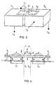
- the test heads T 1 , T 2 are identical in construction here, which is advisable for economic reasons, and have the shape 2.
- the decentralized connection field F 1 is indicated, the z. B. in an 8 by 8 grid arranged resilient contact needle N (shown in a section in Fig. 4).
- the contact needles N establish the electrical connection to the adapter A 1 , which carries the device under test IC 1 in a jack.
- the peripheral hardware for controlling the test specimen connections is located inside the test head T 1 , since the shortest possible signal paths between the control electronics and test specimen connections are necessary for fast test processes, ie for high test clock frequencies. At the same time, the signal paths to the individual test object connections should be as long as possible, so that there are no skew differences with the result of irregular test results when the test signals are applied.
- the pin electronics have a considerable scope in fast test facilities, e.g. B. per DUT connection.
- a data processor plus data and program memory For reasons of economy, this leads to the demand for maximum use of the test capacity, ie the test sample connections that can be accommodated by a test head.
- the test sample connections that can be accommodated by a test head.
- These conflicting requirements are met by a flexible test facility, the two test heads T 1 , T 2 of which each have a medium test capacity (can accommodate 64 test specimen connections by today's standards) and, if necessary, for testing a more connected test specimen IC (with up to 128 external connections in the example mentioned) work together (see Fig. 3, 4).
- connection fields F 1 , F 2 are of great advantage because the test heads T 1 , T 2 can thereby be set up next to one another with connection fields F 1 , F 2 facing one another, which results in short connection paths to the device under test IC.
- This is placed in the Steckutzaung X of the special adapter S whose plate P both terminal fields F 1, F 2 of the juxtaposed test heads T 1, T 2 is covered, is fixed by centering pins Y to the test heads T 1, T 2 and in the grid of Connection fields F 1 , F 2 arranged connection contacts K with the spring contact pins N of the pin electronics of both test heads T 1 , T 2 is electrically connected.
- the main computer H gives the test heads T 1 , T 2 the test program parts which together implement the test program for the connection-rich test object IC.
- a test head T takes over the control of the test sequence and synchronizes the test head T 2 .
- test heads T 1 , T 2 may require the supply of cooling air by fans. .
- the test heads T 1, T 2 according to Figure 3 a thermal short-circuit is excluded, is reproduced in Fig 2 of the path of the cooling air flow L, provided for the test head T 1.
- the test head T 2 is ventilated analogously. Through one of those side surfaces of each test head housing that face away from the associated other test head T 2 , T 1 , the cooling air flows L 1 and L 2 are fed into the test heads T 1 , T 2 and out through the bottom surface of the test head housing.
- test heads T 1 , T 2 can be expediently used in this way, which are also identical in terms of their cooling system.
Abstract
Description
Die Erfindung betrifft eine Einrichtung für die Funktionsprüfung von elektronischen Prüflingen mit einer Vielzahl von Prüflings Anschlüssen, insbesondere von elektronischen Schaltkreisen, mit den Merkmalen des Oberbegriffes von Anspruch 1.The invention relates to a device for the functional test of electronic test objects with a plurality of test object connections, in particular electronic circuits, with the features of the preamble of
Solche Einrichtung sind beispielsweise bekannt aus dem Firmenprospekt Fairchild Product Description 5/81 Nr. 57148901 (LSI Test System).Such devices are known for example from the company brochure Fairchild Product Description 5/81 No. 57148901 (LSI Test System).
Bei integrierten Schaltkreisen besteht sowohl auf der Hersteller- als auch auf der Anwenderebene das Bedürfnis, durch systematische Funktionsprüfungen defekte Produkte zu erkennen : Der Hersteller muß zum einen aus Gründen der Konkurrenzfähigkeit einen hohen Qualitätsstandard seiner Lieferungen sicherstellen und benötigt zum anderen für seinen betriebsintemen Produktionsprozeß Rückmeidedaten; der Anwender will nur einwandfreie Ware bezahlen, die Zuverlässigkeit verschiedener Lieferanten beurteilen können und Störungen in der eigenen Produktion als Folge fehlerhafter Zulieferteile vermeiden.With integrated circuits, there is a need at both the manufacturer and the user level to identify defective products through systematic functional tests: on the one hand, the manufacturer must ensure a high quality standard of his deliveries for reasons of competitiveness and, on the other hand, requires feedback data for his in-house production process; the user only wants to pay for flawless goods, be able to assess the reliability of various suppliers and avoid disruptions in their own production as a result of faulty supplier parts.
Die erreichte und weiterhin zunehmende Komplexität integrierter Schaltkreise - immer mehr Funktionen werden auf einem Halbleiterchip zusammengefaßt - erfordert aus technischen und wirtschaftlichen Gründen eine Automatisierung des Prüfablaufs. In erster Linie ist hierzu der Einsatz von Elektronenrechnern zu zählen, unter deren Kontrolle Prüfprogramme, z. B. bei digital arbeitenden Prüflingen definierte Folgen von Bitmustem, am Prüfling ablaufen. In mechanischer Hinsicht ist die manuelle Zuführung des Prüflings zum Prüfplatz durch Beschickungseinrichtungen, auch Handhabungsautomaten, ersetzbar.The achieved and increasing complexity of integrated circuits - more and more functions are being combined on a semiconductor chip - requires automation of the test sequence for technical and economic reasons. First and foremost, the use of electronic computers is to be counted, under whose control test programs, e.g. B. in digitally working test objects, defined sequences of bit patterns run on the test object. From a mechanical point of view, the manual feeding of the test object to the test station can be replaced by loading devices, including handling machines.
Mit der Komplexität der integrierten Schaltkreise hängt ein weiteres, praktisches Problem direkt zusammen: Die große Zahl extemer Anschlüsse (Pins), die für den Zugriff zu den hochintegrierten Funktionen erforderlich sind, wirft Anordnungs-und Kontaktierungsschwierigkeiten auf.Another, practical problem is directly related to the complexity of the integrated circuits: the large number of external connections (pins) required for access to the highly integrated functions poses arrangement and contacting difficulties.
Speziell bei einer Prüfeinrichtung für integrierte Schaltkreise stellt sich hierbei das Problem, daß sie einerseits hinsichtlich der Zahl der aufzunehmenden Prüflingsanschlüsse maximal dimensioniert sein muß, um auch die anschlußreichsten Prüflinge testen zu können, daß sie andererseits dann aber beim Testen von Prüflingen mit relativ geringer Zahl extemer Anschlüsse unwirtschaftlich arbeitet. Letzterem Nachteil kann auch nicht dadurch begegnet werden, daß am Testplatz eine Vielzahl abgestuft dimensionierter Testköpfe zur Verfügung gehalten werden, da die Mehrzahl dieser kostspieligen Systemkomponenten dauemd brachliegen würde.Especially in the case of a test facility for integrated circuits, the problem arises here that on the one hand it has to be dimensioned to the maximum with regard to the number of test specimen connections to be able to test even the most connected test specimens, but on the other hand they are more extreme when testing test specimens with a relatively small number Connections works uneconomically. The latter disadvantage cannot be countered by having a large number of graduated test heads available at the test station, since the majority of these costly system components would be unused.
Aus der DE-A-31 43 768 ist ein Adapter zum Anschließen der Kontaktpunkte eines Prüflings, insbesondere einer Leiterplatte, an eine Prüfeinrichtung bekannt.. Der Adapter besteht aus einer Zwischenkontaktplatte, einer Rangierplatte und einer weiteren Kontaktplatte. Dabei verbinden die Kontaktstifte der Zwischenkontaktplatte die Prüflingskontakte zunächst mit der Rangierplatte. Auf der Rangierplatte erfolgt insbesondere mittels Drahtverbindungen eine derartige räumliche Umverteilung in der Kontaktanordnung, daß die Rangierplatte schließlich mit den Kontaktmitteln der weiteren Kontaktplatte in Verbindung gebracht werden kann. Von hier wird schließlich der Anschluß der Kontakte an die Prüfeinrichtung hergestellt.From DE-A-31 43 768 an adapter for connecting the contact points of a test object, in particular a printed circuit board, to a test device is known. The adapter consists of an intermediate contact plate, a marshalling plate and a further contact plate. The contact pins of the intermediate contact plate first connect the test object contacts to the patch plate. Such spatial redistribution in the contact arrangement takes place on the marshalling plate, in particular by means of wire connections, that the marshalling plate can finally be connected to the contact means of the further contact plate. From here, the connection of the contacts to the test equipment is finally made.
Der Erfindung liegt daher die Aufgabe zugrunde, eine Einrichtung der eingangs genannten Art so flexibel und wirtschaftlich zu gestalten, daß Prüflinge unterschiedlichster Anschlußzahl unter größtmöglicher Auslastung der vorhandenen Prüfkapazität, nämlich der Zahl der von den Testköpfen aufnehmbaren Prüflingsanschlüsse, prüfbar sind.The invention is therefore based on the object of designing a device of the type mentioned at the outset so flexibly and economically that test objects of the most varied number of connections can be tested with the greatest possible utilization of the available test capacity, namely the number of test object connections which can be accommodated by the test heads.
Diese Aufgabe wird durch die kennzeichnenden Merkmale des Anspruchs 1 gelöst. Vorteilhafte weitere Ausgestaltungen dieser Lösung sind Gegenstand der weiteren Ansprüche.This object is achieved by the characterizing features of
Der Vorteil der erfindungsgemäßen Lösungen besteht in der Flexibilität der Prüfeinrichtung hinsichtlich der Prüfung von Prüflingen unterschiedlichster Anschlußzahl und der damit einhergehenden wirtschaftlichen Nutzbarkeit der Prüfkapazität der Testköpfe. Dabei weist die Lösung nach Anspruch 1 - bei vorgegebener Prüfkapazität - als immanenten Vorteil noch die Option auf, bei Bedarf mehrere räumlich getrennte Testplätze einzurichten.The advantage of the solutions according to the invention lies in the flexibility of the test device with regard to the testing of test objects of the most varied number of connections and the associated economic usability of the test capacity of the test heads. The solution according to claim 1 - with a given test capacity - also has the inherent advantage of the option to set up several spatially separated test stations if necessary.
Die Ausgestaltung der Testköpfe nach Anspruch 2, nämlich die außermittige Anordnung ihrer Anschlußfelder, hat den Vorteil, daß diese bei nebeneinander stehenden Testköpfen so nahe wie möglich beieinander liegen, wodurch der zugehörige Sonderadapter kleinere Abmessungen aufweist und der Anschlußweg zwischen Prüfling und Testköpfen minimal wird, was für hohe Prüftaktfrequenzen eine notwendige Forderung darstellt.The design of the test heads according to claim 2, namely the eccentric arrangement of their connection fields, has the advantage that they are as close together as possible when the test heads are next to one another, as a result of which the associated special adapter has smaller dimensions and the connection path between the device under test and test heads is minimal, which is what is a necessary requirement for high test clock frequencies.
Die Merkmale des Anspruches 3 ergeben eine vorteilhafte An- und Abschließbarkeit zwischen Prüfling(en) und Sonderadapter einerseits und zwischen Sonderadapter und Testköpfen (Testkopf) andererseits.The features of claim 3 result in an advantageous connectability and lockability between the test object (s) and special adapter on the one hand and between special adapter and test heads (test head) on the other.
Der Vorteil der Kühlluftstromlenkung nach Anspruch 4 liegt in der Vermeidung von Wärmekurzschlüssen nebeneinander aufgesteller Testköpfe.The advantage of the cooling air flow control according to claim 4 lies in the avoidance of heat short circuits of test heads placed next to one another.
Der Anspruch 5 beinhaltet eine besonders vorteilhafte Prüfablauforganisation.Claim 5 contains a particularly advantageous test sequence organization.
Anhand der in den Zeichnungen dargestellten Ausführungsbeispiele wird die Erfindung näher erläutert. Es zeigen :
- Fig. 1 in schematischer Form eine Testeinrichtung mit zwei an einen Hauptrechner gekoppelten Testköpfen,
- Fig. 2 einen Testkopf in Einzelbetrieb,
- Fig. 3 zwei Testköpfe in Tandem-Konfiguration zur Prüfung eines anschlußreichen Prüflings,
- Fig. 4 ein Schnittbild der Anordnung aus Fig. 3.
- 1 in schematic form a test device with two test heads coupled to a main computer,
- 2 a test head in individual operation,
- 3 two test heads in tandem configuration for testing a connection-rich test object,
- FIG. 4 shows a sectional view of the arrangement from FIG. 3.
Die Testeinrichtung nach Fig. 1 besteht aus einem Hauptrechner H und den Testköpfen T1, T2. Der Hauptrechner H speichert Prüfprogramme, delegiert sie an die Testköpfe, überwacht die Prüfabläufe, erstellt Prüfprotokolle und -statistiken, steuert etwaige Beschickungseinrichtungen usw. Die Testköpfe T1, T2 sind hier baugleich angenommen, was sich aus wirtschaftlichen Gründen empfiehlt, und besitzen die Gestalt gemäß Fig. 2. Auf der Oberseite des beispielhaft gezeigten Testkopfes T1 ist dessen dezentrales Anschlußfeld F1 angedeutet, das z. B. in einem 8mal 8-Raster angeordnete federnde Kontaktnadein N (in einem Schnitt dargestellt in Fig. 4) bilden. Die Kontaktnadeln N stellen die elektrische Verbindung zum Adapter A1 her, der in einer Steckfassung den Prüfling IC1 trägt. Im Inneren des Testkopfes T1 befindet sich die periphere Hardware zur Ansteuerung der Prüflingsanschlüsse (Pin-Elektronik), da für schnelle Prüfvorgänge, d. h. für hohe Prüftaktfrequenzen, möglichst kurze Signalwege zwischen Ansteuerelektronik und Prüflingsanschlüssen notwendig sind. Gleichzeitig sollen die Signalwege zu den einzelnen Prüflingsanschlüssen möglichst gleich lang sein, damit es beim Anlegen der Prüfsignale nicht zu Laufzeitunterschieden (skew) mit der Folge irregulärer Testergebnisse kommt.1 consists of a main computer H and the test heads T 1 , T 2 . The main computer H stores test programs, delegates them to the test heads, monitors the test sequences, creates test protocols and statistics, controls any loading devices, etc. The test heads T 1 , T 2 are identical in construction here, which is advisable for economic reasons, and have the shape 2. On the top of the test head T 1 shown as an example, the decentralized connection field F 1 is indicated, the z. B. in an 8 by 8 grid arranged resilient contact needle N (shown in a section in Fig. 4). The contact needles N establish the electrical connection to the adapter A 1 , which carries the device under test IC 1 in a jack. The peripheral hardware for controlling the test specimen connections (pin electronics) is located inside the test head T 1 , since the shortest possible signal paths between the control electronics and test specimen connections are necessary for fast test processes, ie for high test clock frequencies. At the same time, the signal paths to the individual test object connections should be as long as possible, so that there are no skew differences with the result of irregular test results when the test signals are applied.
Die Pin-Elektronik weist in schnellen Testeinrichtungen einen erheblichen Umfang auf, z. B. pro Prüflingsanschluß .einen Datenprozessor zuzüglich Daten- und Programmspeichem. Daraus leitet sich aus Wirtschaftlichkeitsgründen die Forderung nach maximaler Nutzung der Prüfkapazität, d. h. der von einem Testkopf aufnehmbaren Prüflingsanschlüsse, ab. Zugleich besteht aber das Bedürfnis, in einer vorhandenen Testeinrichtung Prüflinge mit unterschiedlichster Zahl von Anschlüssen prüfen zu können. Diese gegensätzlichen Forderungen werden von einer flexiblen Testeinrichtung erfüllt, deren zwei Testköpfe T1, T2 jeweils eine mittlere Prüfkapazität aufweisen (nach heutigen Maßstäben z. B. 64 Prüflingsanschlüsse aufnehmen können) und bei Bedarf zur Prüfung eines anschlußreicheren Prüflings IC (mit bis zu 128 extemen Anschlüssen im genannten Beispiel) zusammenarbeiten (siehe Fig. 3, 4). Für diesen Zweck ist die aussermittige Anordnung der Anschlußfelder F1, F2 (siehe Fig. 2, 3, 4) von großem Vorteil, weil die Testköpfe T1, T2 dadurch mit einander zugewandten Anschlußfeldem F1, F2 nebeneinander aufstellbar sind, wodurch sich kurze Anschlußwege zum Prüfling IC ergeben. Dieser wird in der Steckfassaung X des Sonderadapters S plaziert, dessen Platte P beide Anschlußfelder F1, F2 der nebeneinander stehenden Testköpfe T1, T2 überdeckt, über Zentrierstifte Y an den Testköpfen T1, T2 fixiert ist und über im Raster der Anschlußfelder F1, F2 angeordnete Anschlußkontakte K mit den fedemden Kontaktnadeln N der Pin-Elektronik beider Testköpfe T1, T2 elektrisch verbunden ist.The pin electronics have a considerable scope in fast test facilities, e.g. B. per DUT connection. A data processor plus data and program memory. For reasons of economy, this leads to the demand for maximum use of the test capacity, ie the test sample connections that can be accommodated by a test head. At the same time, however, there is a need to be able to test specimens with a wide variety of connections in an existing test facility. These conflicting requirements are met by a flexible test facility, the two test heads T 1 , T 2 of which each have a medium test capacity (can accommodate 64 test specimen connections by today's standards) and, if necessary, for testing a more connected test specimen IC (with up to 128 external connections in the example mentioned) work together (see Fig. 3, 4). For this purpose, the eccentric arrangement of the connection fields F 1 , F 2 (see FIGS. 2, 3, 4) is of great advantage because the test heads T 1 , T 2 can thereby be set up next to one another with connection fields F 1 , F 2 facing one another, which results in short connection paths to the device under test IC. This is placed in the Steckfassaung X of the special adapter S whose plate P both terminal fields F 1, F 2 of the juxtaposed test heads T 1, T 2 is covered, is fixed by centering pins Y to the test heads T 1, T 2 and in the grid of Connection fields F 1 , F 2 arranged connection contacts K with the spring contact pins N of the pin electronics of both test heads T 1 , T 2 is electrically connected.
Der Hauptrechner H gibt den Testköpfen T1, T2 die Prüfprogrammteile vor, die zusammen das Prüfprogramm für den anschlußreichen Prüfling IC realisieren. Ein Testkopf T, übernimmt die Führung des Prüfablaufs und synchronisiert den Testkopf T2.The main computer H gives the test heads T 1 , T 2 the test program parts which together implement the test program for the connection-rich test object IC. A test head T takes over the control of the test sequence and synchronizes the test head T 2 .
Die umfangreiche Elektronik in den Testköpfen T1, T2 bedarf u.U. der Zufuhr von Kühlluft durch Gebläse. Damit bei der Tandem-Aufstellung der Testköpfe T1, T2 gemäß Fig. 3 ein Wärmekurzschluß ausgeschlossen ist, ist der in Fig. 2 wiedergegebene Weg des Kühlluftstroms L, für den Testkopf T1 vorgesehen ; der Testkopf T2 wird analog belüftet. Durch eine derjenigen Seitenflächen jedes Testkopfgehäuses, die dem beigeordneten anderen Testkopf T2, T1 abgewandt sind, werden die Kühlluftströme L1 bzw. L2 in die Testköpfe T1, T2 hinein- und jeweils durch die Bodenfläche der Testkopfgehäuse wieder herausgeführt. Die Orientierung der Kühlluftströme L1, L2 ist dabei von untergeordneter Bedeutung, sie muß nur für beide Testköpfe T1, T2 die gleiche sein, da sonst ein Testkopf die Abluft des anderen Testkopfes ansaugt. Jedenfalls lassen sich auf diese Weise zweckmäßig Testköpfe T1, T2 einsetzen, die auch hinsichtlich ihres Kühlsystems baugleich sind.The extensive electronics in the test heads T 1 , T 2 may require the supply of cooling air by fans. . Thus, in the tandem-formation, the test heads T 1, T 2 according to Figure 3, a thermal short-circuit is excluded, is reproduced in Fig 2 of the path of the cooling air flow L, provided for the test head T 1. the test head T 2 is ventilated analogously. Through one of those side surfaces of each test head housing that face away from the associated other test head T 2 , T 1 , the cooling air flows L 1 and L 2 are fed into the test heads T 1 , T 2 and out through the bottom surface of the test head housing. The orientation of the cooling air flows L 1 , L 2 is of minor importance, it only has to be the same for both test heads T 1 , T 2 , otherwise a test head sucks in the exhaust air from the other test head. In any case, test heads T 1 , T 2 can be expediently used in this way, which are also identical in terms of their cooling system.
Claims (5)
Priority Applications (1)
| Application Number | Priority Date | Filing Date | Title |
|---|---|---|---|
| AT85111384T ATE49303T1 (en) | 1984-09-21 | 1985-09-09 | EQUIPMENT FOR FUNCTIONAL TESTING OF INTEGRATED CIRCUITS. |
Applications Claiming Priority (2)
| Application Number | Priority Date | Filing Date | Title |
|---|---|---|---|
| DE3434749 | 1984-09-21 | ||
| DE3434749 | 1984-09-21 |
Publications (2)
| Publication Number | Publication Date |
|---|---|
| EP0175995A1 EP0175995A1 (en) | 1986-04-02 |
| EP0175995B1 true EP0175995B1 (en) | 1990-01-03 |
Family
ID=6246023
Family Applications (1)
| Application Number | Title | Priority Date | Filing Date |
|---|---|---|---|
| EP85111384A Expired - Lifetime EP0175995B1 (en) | 1984-09-21 | 1985-09-09 | Arrangement for testing integrated circuits |
Country Status (5)
| Country | Link |
|---|---|
| US (1) | US4868493A (en) |
| EP (1) | EP0175995B1 (en) |
| JP (1) | JPS6180065A (en) |
| AT (1) | ATE49303T1 (en) |
| DE (1) | DE3575206D1 (en) |
Families Citing this family (10)
| Publication number | Priority date | Publication date | Assignee | Title |
|---|---|---|---|---|
| JP2944256B2 (en) * | 1991-06-10 | 1999-08-30 | 三菱電機株式会社 | How to create a debug program |
| US5216361A (en) * | 1991-07-10 | 1993-06-01 | Schlumberger Technologies, Inc. | Modular board test system having wireless receiver |
| US5488292A (en) * | 1993-10-04 | 1996-01-30 | Tokyo Seimitsu Co., Ltd. | Wafer inspecting system |
| JPH08179008A (en) * | 1994-12-22 | 1996-07-12 | Advantest Corp | Test head cooling device |
| DE19627801C1 (en) * | 1996-07-10 | 1998-03-26 | Atg Test Systems Gmbh | Device for testing electrical circuit boards |
| US6335627B1 (en) * | 1998-04-13 | 2002-01-01 | Intel Corporation | Apparatus and method for testing an electronics package substrate |
| US6732053B1 (en) * | 1998-09-30 | 2004-05-04 | Intel Corporation | Method and apparatus for controlling a test cell |
| US6400134B1 (en) | 2000-07-17 | 2002-06-04 | Infineon Technologies North America Corp. | Automated bad socket masking in real-time for test handlers |
| WO2016086504A1 (en) * | 2014-12-02 | 2016-06-09 | 北京空间飞行器总体设计部 | Vacuum thermal performance test device for two-phase fluid loop, and method |
| US10929261B1 (en) * | 2018-06-25 | 2021-02-23 | Amazon Technologies, Inc. | Device diagnosis |
Family Cites Families (14)
| Publication number | Priority date | Publication date | Assignee | Title |
|---|---|---|---|---|
| US3512582A (en) * | 1968-07-15 | 1970-05-19 | Ibm | Immersion cooling system for modularly packaged components |
| SE350874B (en) * | 1970-03-05 | 1972-11-06 | Asea Ab | |
| US3909934A (en) * | 1972-12-02 | 1975-10-07 | Licentia Gmbh | Method of producing a measuring head for measuring electrical components |
| US3842346A (en) * | 1972-12-20 | 1974-10-15 | C Bobbitt | Continuity testing of solid state circuitry during temperature cycling |
| US4045735A (en) * | 1976-02-17 | 1977-08-30 | E-H Research Laboratories, Inc. | Apparatus for testing electronic devices having a high density array of pin leads |
| US4125763A (en) * | 1977-07-15 | 1978-11-14 | Fluke Trendar Corporation | Automatic tester for microprocessor board |
| GB2033668B (en) * | 1978-11-11 | 1983-01-06 | Ferranti Ltd | Circuit assemblies |
| US4411719A (en) * | 1980-02-07 | 1983-10-25 | Westinghouse Electric Corp. | Apparatus and method for tape bonding and testing of integrated circuit chips |
| US4354268A (en) * | 1980-04-03 | 1982-10-12 | Santek, Inc. | Intelligent test head for automatic test system |
| US4402055A (en) * | 1981-01-27 | 1983-08-30 | Westinghouse Electric Corp. | Automatic test system utilizing interchangeable test devices |
| GB2104669A (en) * | 1981-08-06 | 1983-03-09 | Int Computers Ltd | Apparatus for testing electronic devices |
| JPS5832178A (en) * | 1981-08-19 | 1983-02-25 | Advantest Corp | Ic tester |
| DE3143768A1 (en) * | 1981-11-04 | 1983-05-11 | Siemens AG, 1000 Berlin und 8000 München | Adaptor for connecting contact points, arranged in one plane, of a test specimen to the terminals of a test device |
| US4517512A (en) * | 1982-05-24 | 1985-05-14 | Micro Component Technology, Inc. | Integrated circuit test apparatus test head |
-
1985
- 1985-09-09 AT AT85111384T patent/ATE49303T1/en not_active IP Right Cessation
- 1985-09-09 EP EP85111384A patent/EP0175995B1/en not_active Expired - Lifetime
- 1985-09-09 DE DE8585111384T patent/DE3575206D1/en not_active Expired - Fee Related
- 1985-09-19 JP JP60207705A patent/JPS6180065A/en active Pending
-
1988
- 1988-09-27 US US07/250,999 patent/US4868493A/en not_active Expired - Fee Related
Also Published As
| Publication number | Publication date |
|---|---|
| DE3575206D1 (en) | 1990-02-08 |
| JPS6180065A (en) | 1986-04-23 |
| ATE49303T1 (en) | 1990-01-15 |
| EP0175995A1 (en) | 1986-04-02 |
| US4868493A (en) | 1989-09-19 |
Similar Documents
| Publication | Publication Date | Title |
|---|---|---|
| DE19960112B4 (en) | Test arrangement for testing backplanes, subcarrier substrates, or populated printed circuit boards | |
| DE3812654C2 (en) | ||
| EP0285799A2 (en) | Device for the functional electric testing of wiring arrays, in particular of circuit boards | |
| DE102010025760B4 (en) | Device for testing an integrated circuit | |
| EP0175995B1 (en) | Arrangement for testing integrated circuits | |
| EP0838688B1 (en) | Device and procedure for testing printed circuit boards | |
| DE2744299A1 (en) | METHOD OF ALIGNING A ROW OF PROBES TO A ROW OF CONTACTS | |
| DE10320132A1 (en) | Connector cable and method for probing vacuum sealable electronic nodes of an electrical test device | |
| DE10042224C2 (en) | Module test socket for test adapters | |
| EP1583975A1 (en) | Universal-messadapter-system | |
| DE10024875B4 (en) | Component holder system for use with test devices for testing electronic components | |
| DE19638402C2 (en) | Test device for a multi-contact chip | |
| DE4315082A1 (en) | Versatile rotatable connector assembly for testing integrated circuit components | |
| EP0875767B1 (en) | Device and procedure for testing naked circuit boards | |
| DE10302131A1 (en) | Adapter method and device for interfacing a tester with a test object | |
| WO2004059329A1 (en) | Adapter for testing conductor arrangements | |
| DE4223193A1 (en) | Programmable controller with facility for plug in of test unit - allows inputs to be simulated or detection of analogue and digital signals for system testing | |
| DE8427884U1 (en) | Device for the functional test of integrated circuits | |
| DE4100634A1 (en) | TEST DEVICE | |
| DE112021001124T5 (en) | Burn-In Board Including Strip Socket With Integrated Heater For Burning In Semiconductor Components On A Large Scale | |
| DE2938567A1 (en) | Highly integrated semiconductor device - has housing with fine connecting wires and thicker conductors for both operating and testing contacts | |
| DE112007001936B4 (en) | Extended package substrate and method for coupling a substrate of an IC package to a socket | |
| DE3724144A1 (en) | Arrangement for testing circuits which are integrated on a chip | |
| DE2051052A1 (en) | Testing device for testing etched circuit boards | |
| EP0372666A1 (en) | Multicompatible holding fixture for printed-circuit boards or SMT devices to be tested, and for contact boards and supporting boards for use in testing apparatuses |
Legal Events
| Date | Code | Title | Description |
|---|---|---|---|
| PUAI | Public reference made under article 153(3) epc to a published international application that has entered the european phase |
Free format text: ORIGINAL CODE: 0009012 |
|
| AK | Designated contracting states |
Kind code of ref document: A1 Designated state(s): AT BE CH DE FR GB IT LI LU NL SE |
|
| 17P | Request for examination filed |
Effective date: 19860507 |
|
| 17Q | First examination report despatched |
Effective date: 19880224 |
|
| GRAA | (expected) grant |
Free format text: ORIGINAL CODE: 0009210 |
|
| AK | Designated contracting states |
Kind code of ref document: B1 Designated state(s): AT BE CH DE FR GB IT LI LU NL SE |
|
| PG25 | Lapsed in a contracting state [announced via postgrant information from national office to epo] |
Ref country code: SE Effective date: 19900103 |
|
| REF | Corresponds to: |
Ref document number: 49303 Country of ref document: AT Date of ref document: 19900115 Kind code of ref document: T |
|
| REF | Corresponds to: |
Ref document number: 3575206 Country of ref document: DE Date of ref document: 19900208 |
|
| ET | Fr: translation filed | ||
| ITF | It: translation for a ep patent filed |
Owner name: STUDIO JAUMANN |
|
| GBT | Gb: translation of ep patent filed (gb section 77(6)(a)/1977) | ||
| PGFP | Annual fee paid to national office [announced via postgrant information from national office to epo] |
Ref country code: BE Payment date: 19900913 Year of fee payment: 6 Ref country code: GB Payment date: 19900913 Year of fee payment: 6 |
|
| PGFP | Annual fee paid to national office [announced via postgrant information from national office to epo] |
Ref country code: FR Payment date: 19900925 Year of fee payment: 6 |
|
| PGFP | Annual fee paid to national office [announced via postgrant information from national office to epo] |
Ref country code: AT Payment date: 19900928 Year of fee payment: 6 |
|
| ITTA | It: last paid annual fee | ||
| PG25 | Lapsed in a contracting state [announced via postgrant information from national office to epo] |
Ref country code: LU Free format text: LAPSE BECAUSE OF NON-PAYMENT OF DUE FEES Effective date: 19900930 |
|
| PGFP | Annual fee paid to national office [announced via postgrant information from national office to epo] |
Ref country code: NL Payment date: 19900930 Year of fee payment: 6 |
|
| PGFP | Annual fee paid to national office [announced via postgrant information from national office to epo] |
Ref country code: LU Payment date: 19901005 Year of fee payment: 6 |
|
| PLBE | No opposition filed within time limit |
Free format text: ORIGINAL CODE: 0009261 |
|
| STAA | Information on the status of an ep patent application or granted ep patent |
Free format text: STATUS: NO OPPOSITION FILED WITHIN TIME LIMIT |
|
| PGFP | Annual fee paid to national office [announced via postgrant information from national office to epo] |
Ref country code: DE Payment date: 19901126 Year of fee payment: 6 |
|
| PGFP | Annual fee paid to national office [announced via postgrant information from national office to epo] |
Ref country code: CH Payment date: 19901217 Year of fee payment: 6 |
|
| 26N | No opposition filed | ||
| PG25 | Lapsed in a contracting state [announced via postgrant information from national office to epo] |
Ref country code: AT Effective date: 19910909 Ref country code: GB Effective date: 19910909 |
|
| PG25 | Lapsed in a contracting state [announced via postgrant information from national office to epo] |
Ref country code: LI Effective date: 19910930 Ref country code: BE Effective date: 19910930 Ref country code: CH Effective date: 19910930 |
|
| BERE | Be: lapsed |
Owner name: SIEMENS A.G. Effective date: 19910930 |
|
| PG25 | Lapsed in a contracting state [announced via postgrant information from national office to epo] |
Ref country code: NL Effective date: 19920401 |
|
| GBPC | Gb: european patent ceased through non-payment of renewal fee | ||
| NLV4 | Nl: lapsed or anulled due to non-payment of the annual fee | ||
| PG25 | Lapsed in a contracting state [announced via postgrant information from national office to epo] |
Ref country code: FR Effective date: 19920529 |
|
| REG | Reference to a national code |
Ref country code: CH Ref legal event code: PL |
|
| PG25 | Lapsed in a contracting state [announced via postgrant information from national office to epo] |
Ref country code: DE Effective date: 19920602 |
|
| REG | Reference to a national code |
Ref country code: FR Ref legal event code: ST |