EP0175995B1 - Dispositif pour tester le fonctionnement des circuits intégrés - Google Patents
Dispositif pour tester le fonctionnement des circuits intégrés Download PDFInfo
- Publication number
- EP0175995B1 EP0175995B1 EP85111384A EP85111384A EP0175995B1 EP 0175995 B1 EP0175995 B1 EP 0175995B1 EP 85111384 A EP85111384 A EP 85111384A EP 85111384 A EP85111384 A EP 85111384A EP 0175995 B1 EP0175995 B1 EP 0175995B1
- Authority
- EP
- European Patent Office
- Prior art keywords
- test
- heads
- connection area
- head
- arrangement
- Prior art date
- Legal status (The legal status is an assumption and is not a legal conclusion. Google has not performed a legal analysis and makes no representation as to the accuracy of the status listed.)
- Expired - Lifetime
Links
Images

Classifications
-
- G—PHYSICS
- G01—MEASURING; TESTING
- G01R—MEASURING ELECTRIC VARIABLES; MEASURING MAGNETIC VARIABLES
- G01R1/00—Details of instruments or arrangements of the types included in groups G01R5/00 - G01R13/00 and G01R31/00
- G01R1/02—General constructional details
- G01R1/06—Measuring leads; Measuring probes
- G01R1/067—Measuring probes
- G01R1/073—Multiple probes
- G01R1/07307—Multiple probes with individual probe elements, e.g. needles, cantilever beams or bump contacts, fixed in relation to each other, e.g. bed of nails fixture or probe card
- G01R1/07314—Multiple probes with individual probe elements, e.g. needles, cantilever beams or bump contacts, fixed in relation to each other, e.g. bed of nails fixture or probe card the body of the probe being perpendicular to test object, e.g. bed of nails or probe with bump contacts on a rigid support
Definitions
- the invention relates to a device for the functional test of electronic test objects with a plurality of test object connections, in particular electronic circuits, with the features of the preamble of claim 1.
- an adapter for connecting the contact points of a test object, in particular a printed circuit board, to a test device is known.
- the adapter consists of an intermediate contact plate, a marshalling plate and a further contact plate.
- the contact pins of the intermediate contact plate first connect the test object contacts to the patch plate.
- Such spatial redistribution in the contact arrangement takes place on the marshalling plate, in particular by means of wire connections, that the marshalling plate can finally be connected to the contact means of the further contact plate. From here, the connection of the contacts to the test equipment is finally made.
- the invention is therefore based on the object of designing a device of the type mentioned at the outset so flexibly and economically that test objects of the most varied number of connections can be tested with the greatest possible utilization of the available test capacity, namely the number of test object connections which can be accommodated by the test heads.
- the advantage of the solutions according to the invention lies in the flexibility of the test device with regard to the testing of test objects of the most varied number of connections and the associated economic usability of the test capacity of the test heads.
- the solution according to claim 1 - with a given test capacity - also has the inherent advantage of the option to set up several spatially separated test stations if necessary.
- test heads according to claim 2 namely the eccentric arrangement of their connection fields, has the advantage that they are as close together as possible when the test heads are next to one another, as a result of which the associated special adapter has smaller dimensions and the connection path between the device under test and test heads is minimal, which is what is a necessary requirement for high test clock frequencies.
- the advantage of the cooling air flow control according to claim 4 lies in the avoidance of heat short circuits of test heads placed next to one another.
- Claim 5 contains a particularly advantageous test sequence organization.
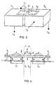
- test head 1 consists of a main computer H and the test heads T 1 , T 2 .
- the main computer H stores test programs, delegates them to the test heads, monitors the test sequences, creates test protocols and statistics, controls any loading devices, etc.
- the test heads T 1 , T 2 are identical in construction here, which is advisable for economic reasons, and have the shape 2.
- the decentralized connection field F 1 is indicated, the z. B. in an 8 by 8 grid arranged resilient contact needle N (shown in a section in Fig. 4).
- the contact needles N establish the electrical connection to the adapter A 1 , which carries the device under test IC 1 in a jack.
- the peripheral hardware for controlling the test specimen connections is located inside the test head T 1 , since the shortest possible signal paths between the control electronics and test specimen connections are necessary for fast test processes, ie for high test clock frequencies. At the same time, the signal paths to the individual test object connections should be as long as possible, so that there are no skew differences with the result of irregular test results when the test signals are applied.
- the pin electronics have a considerable scope in fast test facilities, e.g. B. per DUT connection.
- a data processor plus data and program memory For reasons of economy, this leads to the demand for maximum use of the test capacity, ie the test sample connections that can be accommodated by a test head.
- the test sample connections that can be accommodated by a test head.
- These conflicting requirements are met by a flexible test facility, the two test heads T 1 , T 2 of which each have a medium test capacity (can accommodate 64 test specimen connections by today's standards) and, if necessary, for testing a more connected test specimen IC (with up to 128 external connections in the example mentioned) work together (see Fig. 3, 4).
- connection fields F 1 , F 2 are of great advantage because the test heads T 1 , T 2 can thereby be set up next to one another with connection fields F 1 , F 2 facing one another, which results in short connection paths to the device under test IC.
- This is placed in the Steckutzaung X of the special adapter S whose plate P both terminal fields F 1, F 2 of the juxtaposed test heads T 1, T 2 is covered, is fixed by centering pins Y to the test heads T 1, T 2 and in the grid of Connection fields F 1 , F 2 arranged connection contacts K with the spring contact pins N of the pin electronics of both test heads T 1 , T 2 is electrically connected.
- the main computer H gives the test heads T 1 , T 2 the test program parts which together implement the test program for the connection-rich test object IC.
- a test head T takes over the control of the test sequence and synchronizes the test head T 2 .
- test heads T 1 , T 2 may require the supply of cooling air by fans. .
- the test heads T 1, T 2 according to Figure 3 a thermal short-circuit is excluded, is reproduced in Fig 2 of the path of the cooling air flow L, provided for the test head T 1.
- the test head T 2 is ventilated analogously. Through one of those side surfaces of each test head housing that face away from the associated other test head T 2 , T 1 , the cooling air flows L 1 and L 2 are fed into the test heads T 1 , T 2 and out through the bottom surface of the test head housing.
- test heads T 1 , T 2 can be expediently used in this way, which are also identical in terms of their cooling system.
Landscapes
- Physics & Mathematics (AREA)
- General Physics & Mathematics (AREA)
- Testing Of Individual Semiconductor Devices (AREA)
- Testing Of Short-Circuits, Discontinuities, Leakage, Or Incorrect Line Connections (AREA)
- Tests Of Electronic Circuits (AREA)
- Semiconductor Integrated Circuits (AREA)
Claims (5)
Priority Applications (1)
| Application Number | Priority Date | Filing Date | Title |
|---|---|---|---|
| AT85111384T ATE49303T1 (de) | 1984-09-21 | 1985-09-09 | Einrichtung fuer die funktionspruefung integrierter schaltkreise. |
Applications Claiming Priority (2)
| Application Number | Priority Date | Filing Date | Title |
|---|---|---|---|
| DE3434749 | 1984-09-21 | ||
| DE3434749 | 1984-09-21 |
Publications (2)
| Publication Number | Publication Date |
|---|---|
| EP0175995A1 EP0175995A1 (fr) | 1986-04-02 |
| EP0175995B1 true EP0175995B1 (fr) | 1990-01-03 |
Family
ID=6246023
Family Applications (1)
| Application Number | Title | Priority Date | Filing Date |
|---|---|---|---|
| EP85111384A Expired - Lifetime EP0175995B1 (fr) | 1984-09-21 | 1985-09-09 | Dispositif pour tester le fonctionnement des circuits intégrés |
Country Status (5)
| Country | Link |
|---|---|
| US (1) | US4868493A (fr) |
| EP (1) | EP0175995B1 (fr) |
| JP (1) | JPS6180065A (fr) |
| AT (1) | ATE49303T1 (fr) |
| DE (1) | DE3575206D1 (fr) |
Families Citing this family (10)
| Publication number | Priority date | Publication date | Assignee | Title |
|---|---|---|---|---|
| JP2944256B2 (ja) * | 1991-06-10 | 1999-08-30 | 三菱電機株式会社 | デバッグ用プログラム作成方法 |
| US5216361A (en) * | 1991-07-10 | 1993-06-01 | Schlumberger Technologies, Inc. | Modular board test system having wireless receiver |
| US5488292A (en) * | 1993-10-04 | 1996-01-30 | Tokyo Seimitsu Co., Ltd. | Wafer inspecting system |
| JPH08179008A (ja) * | 1994-12-22 | 1996-07-12 | Advantest Corp | テスト・ヘッド冷却装置 |
| DE19627801C1 (de) * | 1996-07-10 | 1998-03-26 | Atg Test Systems Gmbh | Vorrichtung zum Prüfen von elektrischen Leiterplatten |
| US6335627B1 (en) * | 1998-04-13 | 2002-01-01 | Intel Corporation | Apparatus and method for testing an electronics package substrate |
| US6732053B1 (en) * | 1998-09-30 | 2004-05-04 | Intel Corporation | Method and apparatus for controlling a test cell |
| US6400134B1 (en) | 2000-07-17 | 2002-06-04 | Infineon Technologies North America Corp. | Automated bad socket masking in real-time for test handlers |
| EP3229015B1 (fr) * | 2014-12-02 | 2019-10-30 | Beijing Institute of Spacecraft System Engineering | Dispositif de test de performance thermique sous vide pour une boucle de fluide à deux phases et procédé |
| US10929261B1 (en) * | 2018-06-25 | 2021-02-23 | Amazon Technologies, Inc. | Device diagnosis |
Family Cites Families (14)
| Publication number | Priority date | Publication date | Assignee | Title |
|---|---|---|---|---|
| US3512582A (en) * | 1968-07-15 | 1970-05-19 | Ibm | Immersion cooling system for modularly packaged components |
| SE350874B (fr) * | 1970-03-05 | 1972-11-06 | Asea Ab | |
| US3909934A (en) * | 1972-12-02 | 1975-10-07 | Licentia Gmbh | Method of producing a measuring head for measuring electrical components |
| US3842346A (en) * | 1972-12-20 | 1974-10-15 | C Bobbitt | Continuity testing of solid state circuitry during temperature cycling |
| US4045735A (en) * | 1976-02-17 | 1977-08-30 | E-H Research Laboratories, Inc. | Apparatus for testing electronic devices having a high density array of pin leads |
| US4125763A (en) * | 1977-07-15 | 1978-11-14 | Fluke Trendar Corporation | Automatic tester for microprocessor board |
| GB2033668B (en) * | 1978-11-11 | 1983-01-06 | Ferranti Ltd | Circuit assemblies |
| US4411719A (en) * | 1980-02-07 | 1983-10-25 | Westinghouse Electric Corp. | Apparatus and method for tape bonding and testing of integrated circuit chips |
| US4354268A (en) * | 1980-04-03 | 1982-10-12 | Santek, Inc. | Intelligent test head for automatic test system |
| US4402055A (en) * | 1981-01-27 | 1983-08-30 | Westinghouse Electric Corp. | Automatic test system utilizing interchangeable test devices |
| GB2104669A (en) * | 1981-08-06 | 1983-03-09 | Int Computers Ltd | Apparatus for testing electronic devices |
| JPS5832178A (ja) * | 1981-08-19 | 1983-02-25 | Advantest Corp | Icテスタ |
| DE3143768A1 (de) * | 1981-11-04 | 1983-05-11 | Siemens AG, 1000 Berlin und 8000 München | Adapter zur verbindung von in einer ebene angeordneten kontaktpunkten eines prueflings mit den anschluessen einer pruefeinrichtung |
| US4517512A (en) * | 1982-05-24 | 1985-05-14 | Micro Component Technology, Inc. | Integrated circuit test apparatus test head |
-
1985
- 1985-09-09 AT AT85111384T patent/ATE49303T1/de not_active IP Right Cessation
- 1985-09-09 DE DE8585111384T patent/DE3575206D1/de not_active Expired - Fee Related
- 1985-09-09 EP EP85111384A patent/EP0175995B1/fr not_active Expired - Lifetime
- 1985-09-19 JP JP60207705A patent/JPS6180065A/ja active Pending
-
1988
- 1988-09-27 US US07/250,999 patent/US4868493A/en not_active Expired - Fee Related
Also Published As
| Publication number | Publication date |
|---|---|
| EP0175995A1 (fr) | 1986-04-02 |
| US4868493A (en) | 1989-09-19 |
| DE3575206D1 (de) | 1990-02-08 |
| JPS6180065A (ja) | 1986-04-23 |
| ATE49303T1 (de) | 1990-01-15 |
Similar Documents
| Publication | Publication Date | Title |
|---|---|---|
| DE19960112B4 (de) | Testanordnung zum Testen von Rückwandplatinen, Zwischenträgersubstraten, oder bestückten Leiterplatten | |
| DE3812654C2 (fr) | ||
| EP0285799A2 (fr) | Dispositif de test électrique du fonctionnement de rangées de fils électriques, en particulier pour cartes de circuit | |
| DE102010025760B4 (de) | Vorrichtung zum Testen einer integrierten Schaltung | |
| US5387861A (en) | Programmable low profile universally selectable burn-in board assembly | |
| EP0175995B1 (fr) | Dispositif pour tester le fonctionnement des circuits intégrés | |
| EP0838688B1 (fr) | Appareil et procédé de test de circuits imprimés | |
| DE2744299A1 (de) | Verfahren zum ausrichten einer reihe von sonden auf eine reihe von kontakten | |
| DE10320132A1 (de) | Verbinderkabel und Verfahren zum Sondieren von vakuumabdichtbaren elektronischen Knoten einer elektrischen Testvorrichtung | |
| DE10042224C2 (de) | Modultestsockel für Prüfadapter | |
| EP1583975A1 (fr) | Systeme d'adaptateur de mesure universel | |
| DE10024875B4 (de) | Bauteilhaltersystem zur Verwendung mit Testvorrichtungen zum Testen elektronischer Bauteile | |
| DE19638402C2 (de) | Prüfvorrichtung für einen Mehrkontakt-Chip | |
| DE4315082A1 (de) | Vielfältig einsetzbare drehbare Verbinderanordnung zum Testen integrierter Schaltungsbausteine | |
| EP0875767B1 (fr) | Appareil et procédé pour tester des circuits imprimés non pourvus de composants | |
| DE19931278A1 (de) | Prüfkarte für IC-Prüfgerät | |
| DE10302131A1 (de) | Adapterverfahren und Vorrichtung zum schnittstellenmässigen Verbinden eines Testers mit einem Testobjekt | |
| DE4223193A1 (de) | Programmierbare Steuerung mit Anschlußeinheiten zur Verbindung mit analogen und/oder digitalen Peripheriegeräten | |
| DE8427884U1 (de) | Einrichtung für die Funktionsprüfung integrierter Schaltkreise | |
| DE4100634A1 (de) | Pruefvorrichtung | |
| DE112021001124T5 (de) | Einbrenn-Platine Einschliesslich Streifenfassung Mit Integrierter Heizung Zum Einbrennen Von Halbleiterbauelementen In Grossem Umfang | |
| DE112020007801T5 (de) | Testunterstützungsmodul und Verfahren zum Betreiben einer automatischen Testausrüstung | |
| DE2938567A1 (de) | Baustein fuer hochintegrierte schaltkreise | |
| DE112007001936B4 (de) | Erweitertes Gehäusesubstrat und Verfahren zum Koppeln eines Substrates eines IC- Gehäuses mit einem Sockel | |
| DE3724144A1 (de) | Anordnung zum pruefen von auf einem baustein integrierten schaltungen |
Legal Events
| Date | Code | Title | Description |
|---|---|---|---|
| PUAI | Public reference made under article 153(3) epc to a published international application that has entered the european phase |
Free format text: ORIGINAL CODE: 0009012 |
|
| AK | Designated contracting states |
Kind code of ref document: A1 Designated state(s): AT BE CH DE FR GB IT LI LU NL SE |
|
| 17P | Request for examination filed |
Effective date: 19860507 |
|
| 17Q | First examination report despatched |
Effective date: 19880224 |
|
| GRAA | (expected) grant |
Free format text: ORIGINAL CODE: 0009210 |
|
| AK | Designated contracting states |
Kind code of ref document: B1 Designated state(s): AT BE CH DE FR GB IT LI LU NL SE |
|
| PG25 | Lapsed in a contracting state [announced via postgrant information from national office to epo] |
Ref country code: SE Effective date: 19900103 |
|
| REF | Corresponds to: |
Ref document number: 49303 Country of ref document: AT Date of ref document: 19900115 Kind code of ref document: T |
|
| REF | Corresponds to: |
Ref document number: 3575206 Country of ref document: DE Date of ref document: 19900208 |
|
| ET | Fr: translation filed | ||
| ITF | It: translation for a ep patent filed |
Owner name: STUDIO JAUMANN |
|
| GBT | Gb: translation of ep patent filed (gb section 77(6)(a)/1977) | ||
| PGFP | Annual fee paid to national office [announced via postgrant information from national office to epo] |
Ref country code: BE Payment date: 19900913 Year of fee payment: 6 Ref country code: GB Payment date: 19900913 Year of fee payment: 6 |
|
| PGFP | Annual fee paid to national office [announced via postgrant information from national office to epo] |
Ref country code: FR Payment date: 19900925 Year of fee payment: 6 |
|
| PGFP | Annual fee paid to national office [announced via postgrant information from national office to epo] |
Ref country code: AT Payment date: 19900928 Year of fee payment: 6 |
|
| ITTA | It: last paid annual fee | ||
| PG25 | Lapsed in a contracting state [announced via postgrant information from national office to epo] |
Ref country code: LU Free format text: LAPSE BECAUSE OF NON-PAYMENT OF DUE FEES Effective date: 19900930 |
|
| PGFP | Annual fee paid to national office [announced via postgrant information from national office to epo] |
Ref country code: NL Payment date: 19900930 Year of fee payment: 6 |
|
| PGFP | Annual fee paid to national office [announced via postgrant information from national office to epo] |
Ref country code: LU Payment date: 19901005 Year of fee payment: 6 |
|
| PLBE | No opposition filed within time limit |
Free format text: ORIGINAL CODE: 0009261 |
|
| STAA | Information on the status of an ep patent application or granted ep patent |
Free format text: STATUS: NO OPPOSITION FILED WITHIN TIME LIMIT |
|
| PGFP | Annual fee paid to national office [announced via postgrant information from national office to epo] |
Ref country code: DE Payment date: 19901126 Year of fee payment: 6 |
|
| PGFP | Annual fee paid to national office [announced via postgrant information from national office to epo] |
Ref country code: CH Payment date: 19901217 Year of fee payment: 6 |
|
| 26N | No opposition filed | ||
| PG25 | Lapsed in a contracting state [announced via postgrant information from national office to epo] |
Ref country code: AT Effective date: 19910909 Ref country code: GB Effective date: 19910909 |
|
| PG25 | Lapsed in a contracting state [announced via postgrant information from national office to epo] |
Ref country code: LI Effective date: 19910930 Ref country code: BE Effective date: 19910930 Ref country code: CH Effective date: 19910930 |
|
| BERE | Be: lapsed |
Owner name: SIEMENS A.G. Effective date: 19910930 |
|
| PG25 | Lapsed in a contracting state [announced via postgrant information from national office to epo] |
Ref country code: NL Effective date: 19920401 |
|
| GBPC | Gb: european patent ceased through non-payment of renewal fee | ||
| NLV4 | Nl: lapsed or anulled due to non-payment of the annual fee | ||
| PG25 | Lapsed in a contracting state [announced via postgrant information from national office to epo] |
Ref country code: FR Effective date: 19920529 |
|
| REG | Reference to a national code |
Ref country code: CH Ref legal event code: PL |
|
| PG25 | Lapsed in a contracting state [announced via postgrant information from national office to epo] |
Ref country code: DE Effective date: 19920602 |
|
| REG | Reference to a national code |
Ref country code: FR Ref legal event code: ST |