CN108058373B - System and method for additive manufacturing of objects - Google Patents
System and method for additive manufacturing of objects Download PDFInfo
- Publication number
- CN108058373B CN108058373B CN201710358660.0A CN201710358660A CN108058373B CN 108058373 B CN108058373 B CN 108058373B CN 201710358660 A CN201710358660 A CN 201710358660A CN 108058373 B CN108058373 B CN 108058373B
- Authority
- CN
- China
- Prior art keywords
- dispensing
- material composition
- building material
- scan
- layer
- Prior art date
- Legal status (The legal status is an assumption and is not a legal conclusion. Google has not performed a legal analysis and makes no representation as to the accuracy of the status listed.)
- Active
Links
Images


Classifications
-
- B—PERFORMING OPERATIONS; TRANSPORTING
- B29—WORKING OF PLASTICS; WORKING OF SUBSTANCES IN A PLASTIC STATE IN GENERAL
- B29C—SHAPING OR JOINING OF PLASTICS; SHAPING OF MATERIAL IN A PLASTIC STATE, NOT OTHERWISE PROVIDED FOR; AFTER-TREATMENT OF THE SHAPED PRODUCTS, e.g. REPAIRING
- B29C64/00—Additive manufacturing, i.e. manufacturing of three-dimensional [3D] objects by additive deposition, additive agglomeration or additive layering, e.g. by 3D printing, stereolithography or selective laser sintering
- B29C64/30—Auxiliary operations or equipment
- B29C64/386—Data acquisition or data processing for additive manufacturing
-
- B—PERFORMING OPERATIONS; TRANSPORTING
- B29—WORKING OF PLASTICS; WORKING OF SUBSTANCES IN A PLASTIC STATE IN GENERAL
- B29C—SHAPING OR JOINING OF PLASTICS; SHAPING OF MATERIAL IN A PLASTIC STATE, NOT OTHERWISE PROVIDED FOR; AFTER-TREATMENT OF THE SHAPED PRODUCTS, e.g. REPAIRING
- B29C35/00—Heating, cooling or curing, e.g. crosslinking or vulcanising; Apparatus therefor
- B29C35/02—Heating or curing, e.g. crosslinking or vulcanizing during moulding, e.g. in a mould
- B29C35/08—Heating or curing, e.g. crosslinking or vulcanizing during moulding, e.g. in a mould by wave energy or particle radiation
- B29C35/0805—Heating or curing, e.g. crosslinking or vulcanizing during moulding, e.g. in a mould by wave energy or particle radiation using electromagnetic radiation
-
- B—PERFORMING OPERATIONS; TRANSPORTING
- B29—WORKING OF PLASTICS; WORKING OF SUBSTANCES IN A PLASTIC STATE IN GENERAL
- B29C—SHAPING OR JOINING OF PLASTICS; SHAPING OF MATERIAL IN A PLASTIC STATE, NOT OTHERWISE PROVIDED FOR; AFTER-TREATMENT OF THE SHAPED PRODUCTS, e.g. REPAIRING
- B29C64/00—Additive manufacturing, i.e. manufacturing of three-dimensional [3D] objects by additive deposition, additive agglomeration or additive layering, e.g. by 3D printing, stereolithography or selective laser sintering
- B29C64/10—Processes of additive manufacturing
- B29C64/106—Processes of additive manufacturing using only liquids or viscous materials, e.g. depositing a continuous bead of viscous material
- B29C64/112—Processes of additive manufacturing using only liquids or viscous materials, e.g. depositing a continuous bead of viscous material using individual droplets, e.g. from jetting heads
-
- B—PERFORMING OPERATIONS; TRANSPORTING
- B29—WORKING OF PLASTICS; WORKING OF SUBSTANCES IN A PLASTIC STATE IN GENERAL
- B29C—SHAPING OR JOINING OF PLASTICS; SHAPING OF MATERIAL IN A PLASTIC STATE, NOT OTHERWISE PROVIDED FOR; AFTER-TREATMENT OF THE SHAPED PRODUCTS, e.g. REPAIRING
- B29C64/00—Additive manufacturing, i.e. manufacturing of three-dimensional [3D] objects by additive deposition, additive agglomeration or additive layering, e.g. by 3D printing, stereolithography or selective laser sintering
- B29C64/10—Processes of additive manufacturing
- B29C64/165—Processes of additive manufacturing using a combination of solid and fluid materials, e.g. a powder selectively bound by a liquid binder, catalyst, inhibitor or energy absorber
-
- B—PERFORMING OPERATIONS; TRANSPORTING
- B29—WORKING OF PLASTICS; WORKING OF SUBSTANCES IN A PLASTIC STATE IN GENERAL
- B29C—SHAPING OR JOINING OF PLASTICS; SHAPING OF MATERIAL IN A PLASTIC STATE, NOT OTHERWISE PROVIDED FOR; AFTER-TREATMENT OF THE SHAPED PRODUCTS, e.g. REPAIRING
- B29C64/00—Additive manufacturing, i.e. manufacturing of three-dimensional [3D] objects by additive deposition, additive agglomeration or additive layering, e.g. by 3D printing, stereolithography or selective laser sintering
- B29C64/30—Auxiliary operations or equipment
- B29C64/307—Handling of material to be used in additive manufacturing
- B29C64/321—Feeding
- B29C64/336—Feeding of two or more materials
-
- B—PERFORMING OPERATIONS; TRANSPORTING
- B33—ADDITIVE MANUFACTURING TECHNOLOGY
- B33Y—ADDITIVE MANUFACTURING, i.e. MANUFACTURING OF THREE-DIMENSIONAL [3-D] OBJECTS BY ADDITIVE DEPOSITION, ADDITIVE AGGLOMERATION OR ADDITIVE LAYERING, e.g. BY 3-D PRINTING, STEREOLITHOGRAPHY OR SELECTIVE LASER SINTERING
- B33Y10/00—Processes of additive manufacturing
-
- B—PERFORMING OPERATIONS; TRANSPORTING
- B33—ADDITIVE MANUFACTURING TECHNOLOGY
- B33Y—ADDITIVE MANUFACTURING, i.e. MANUFACTURING OF THREE-DIMENSIONAL [3-D] OBJECTS BY ADDITIVE DEPOSITION, ADDITIVE AGGLOMERATION OR ADDITIVE LAYERING, e.g. BY 3-D PRINTING, STEREOLITHOGRAPHY OR SELECTIVE LASER SINTERING
- B33Y30/00—Apparatus for additive manufacturing; Details thereof or accessories therefor
-
- B—PERFORMING OPERATIONS; TRANSPORTING
- B33—ADDITIVE MANUFACTURING TECHNOLOGY
- B33Y—ADDITIVE MANUFACTURING, i.e. MANUFACTURING OF THREE-DIMENSIONAL [3-D] OBJECTS BY ADDITIVE DEPOSITION, ADDITIVE AGGLOMERATION OR ADDITIVE LAYERING, e.g. BY 3-D PRINTING, STEREOLITHOGRAPHY OR SELECTIVE LASER SINTERING
- B33Y50/00—Data acquisition or data processing for additive manufacturing
- B33Y50/02—Data acquisition or data processing for additive manufacturing for controlling or regulating additive manufacturing processes
-
- B—PERFORMING OPERATIONS; TRANSPORTING
- B33—ADDITIVE MANUFACTURING TECHNOLOGY
- B33Y—ADDITIVE MANUFACTURING, i.e. MANUFACTURING OF THREE-DIMENSIONAL [3-D] OBJECTS BY ADDITIVE DEPOSITION, ADDITIVE AGGLOMERATION OR ADDITIVE LAYERING, e.g. BY 3-D PRINTING, STEREOLITHOGRAPHY OR SELECTIVE LASER SINTERING
- B33Y80/00—Products made by additive manufacturing
-
- H—ELECTRICITY
- H05—ELECTRIC TECHNIQUES NOT OTHERWISE PROVIDED FOR
- H05K—PRINTED CIRCUITS; CASINGS OR CONSTRUCTIONAL DETAILS OF ELECTRIC APPARATUS; MANUFACTURE OF ASSEMBLAGES OF ELECTRICAL COMPONENTS
- H05K1/00—Printed circuits
- H05K1/02—Details
- H05K1/09—Use of materials for the conductive, e.g. metallic pattern
- H05K1/092—Dispersed materials, e.g. conductive pastes or inks
-
- H—ELECTRICITY
- H05—ELECTRIC TECHNIQUES NOT OTHERWISE PROVIDED FOR
- H05K—PRINTED CIRCUITS; CASINGS OR CONSTRUCTIONAL DETAILS OF ELECTRIC APPARATUS; MANUFACTURE OF ASSEMBLAGES OF ELECTRICAL COMPONENTS
- H05K1/00—Printed circuits
- H05K1/16—Printed circuits incorporating printed electric components, e.g. printed resistor, capacitor, inductor
-
- H—ELECTRICITY
- H05—ELECTRIC TECHNIQUES NOT OTHERWISE PROVIDED FOR
- H05K—PRINTED CIRCUITS; CASINGS OR CONSTRUCTIONAL DETAILS OF ELECTRIC APPARATUS; MANUFACTURE OF ASSEMBLAGES OF ELECTRICAL COMPONENTS
- H05K3/00—Apparatus or processes for manufacturing printed circuits
- H05K3/10—Apparatus or processes for manufacturing printed circuits in which conductive material is applied to the insulating support in such a manner as to form the desired conductive pattern
- H05K3/12—Apparatus or processes for manufacturing printed circuits in which conductive material is applied to the insulating support in such a manner as to form the desired conductive pattern using thick film techniques, e.g. printing techniques to apply the conductive material or similar techniques for applying conductive paste or ink patterns
- H05K3/1283—After-treatment of the printed patterns, e.g. sintering or curing methods
-
- B—PERFORMING OPERATIONS; TRANSPORTING
- B29—WORKING OF PLASTICS; WORKING OF SUBSTANCES IN A PLASTIC STATE IN GENERAL
- B29C—SHAPING OR JOINING OF PLASTICS; SHAPING OF MATERIAL IN A PLASTIC STATE, NOT OTHERWISE PROVIDED FOR; AFTER-TREATMENT OF THE SHAPED PRODUCTS, e.g. REPAIRING
- B29C35/00—Heating, cooling or curing, e.g. crosslinking or vulcanising; Apparatus therefor
- B29C35/02—Heating or curing, e.g. crosslinking or vulcanizing during moulding, e.g. in a mould
- B29C35/08—Heating or curing, e.g. crosslinking or vulcanizing during moulding, e.g. in a mould by wave energy or particle radiation
- B29C35/0805—Heating or curing, e.g. crosslinking or vulcanizing during moulding, e.g. in a mould by wave energy or particle radiation using electromagnetic radiation
- B29C2035/0827—Heating or curing, e.g. crosslinking or vulcanizing during moulding, e.g. in a mould by wave energy or particle radiation using electromagnetic radiation using UV radiation
-
- B—PERFORMING OPERATIONS; TRANSPORTING
- B29—WORKING OF PLASTICS; WORKING OF SUBSTANCES IN A PLASTIC STATE IN GENERAL
- B29K—INDEXING SCHEME ASSOCIATED WITH SUBCLASSES B29B, B29C OR B29D, RELATING TO MOULDING MATERIALS OR TO MATERIALS FOR MOULDS, REINFORCEMENTS, FILLERS OR PREFORMED PARTS, e.g. INSERTS
- B29K2995/00—Properties of moulding materials, reinforcements, fillers, preformed parts or moulds
- B29K2995/0003—Properties of moulding materials, reinforcements, fillers, preformed parts or moulds having particular electrical or magnetic properties, e.g. piezoelectric
- B29K2995/0005—Conductive
-
- B—PERFORMING OPERATIONS; TRANSPORTING
- B29—WORKING OF PLASTICS; WORKING OF SUBSTANCES IN A PLASTIC STATE IN GENERAL
- B29L—INDEXING SCHEME ASSOCIATED WITH SUBCLASS B29C, RELATING TO PARTICULAR ARTICLES
- B29L2031/00—Other particular articles
- B29L2031/34—Electrical apparatus, e.g. sparking plugs or parts thereof
- B29L2031/3425—Printed circuits
-
- H—ELECTRICITY
- H05—ELECTRIC TECHNIQUES NOT OTHERWISE PROVIDED FOR
- H05K—PRINTED CIRCUITS; CASINGS OR CONSTRUCTIONAL DETAILS OF ELECTRIC APPARATUS; MANUFACTURE OF ASSEMBLAGES OF ELECTRICAL COMPONENTS
- H05K3/00—Apparatus or processes for manufacturing printed circuits
- H05K3/10—Apparatus or processes for manufacturing printed circuits in which conductive material is applied to the insulating support in such a manner as to form the desired conductive pattern
- H05K3/12—Apparatus or processes for manufacturing printed circuits in which conductive material is applied to the insulating support in such a manner as to form the desired conductive pattern using thick film techniques, e.g. printing techniques to apply the conductive material or similar techniques for applying conductive paste or ink patterns
- H05K3/1241—Apparatus or processes for manufacturing printed circuits in which conductive material is applied to the insulating support in such a manner as to form the desired conductive pattern using thick film techniques, e.g. printing techniques to apply the conductive material or similar techniques for applying conductive paste or ink patterns by ink-jet printing or drawing by dispensing
- H05K3/125—Apparatus or processes for manufacturing printed circuits in which conductive material is applied to the insulating support in such a manner as to form the desired conductive pattern using thick film techniques, e.g. printing techniques to apply the conductive material or similar techniques for applying conductive paste or ink patterns by ink-jet printing or drawing by dispensing by ink-jet printing
-
- Y—GENERAL TAGGING OF NEW TECHNOLOGICAL DEVELOPMENTS; GENERAL TAGGING OF CROSS-SECTIONAL TECHNOLOGIES SPANNING OVER SEVERAL SECTIONS OF THE IPC; TECHNICAL SUBJECTS COVERED BY FORMER USPC CROSS-REFERENCE ART COLLECTIONS [XRACs] AND DIGESTS
- Y10—TECHNICAL SUBJECTS COVERED BY FORMER USPC
- Y10T—TECHNICAL SUBJECTS COVERED BY FORMER US CLASSIFICATION
- Y10T428/00—Stock material or miscellaneous articles
- Y10T428/24—Structurally defined web or sheet [e.g., overall dimension, etc.]
- Y10T428/24802—Discontinuous or differential coating, impregnation or bond [e.g., artwork, printing, retouched photograph, etc.]
- Y10T428/24917—Discontinuous or differential coating, impregnation or bond [e.g., artwork, printing, retouched photograph, etc.] including metal layer
Landscapes
- Engineering & Computer Science (AREA)
- Chemical & Material Sciences (AREA)
- Materials Engineering (AREA)
- Manufacturing & Machinery (AREA)
- Physics & Mathematics (AREA)
- Optics & Photonics (AREA)
- Mechanical Engineering (AREA)
- Microelectronics & Electronic Packaging (AREA)
- Health & Medical Sciences (AREA)
- Electromagnetism (AREA)
- Toxicology (AREA)
- Oral & Maxillofacial Surgery (AREA)
- Thermal Sciences (AREA)
- Dispersion Chemistry (AREA)
- Production Of Multi-Layered Print Wiring Board (AREA)
Abstract
A method of additive manufacturing of a three-dimensional object is disclosed. The method includes sequentially forming a plurality of layers, each patterned according to a shape of a cross-section of the object, thereby forming the object. In some embodiments, for at least one of the plurality of layers, the forming of the layer comprises performing a raster scan to dispense at least a first building material composition and performing a vector scan to dispense at least a second building material composition. Performing the vector scan along a path selected to form at least one structure selected from the group consisting of: (i) an elongate structure, (ii) a border structure at least partially surrounding an area filled with the first build material, and (iii) an inter-layer connection structure.
Description
The present application is a divisional application of a patent application with application number 201280023976.X entitled "system and method for additive manufacturing of objects" filed on 17.04.2012.
Cross Reference to Related Applications
The present invention claims priority from U.S. application No.61/476275, filed on 17/4/2011, the contents of which are incorporated herein by reference in their entirety.
Technical Field
The present invention, in some embodiments thereof, relates to Additive Manufacturing (AM) of an object, and more particularly, but not exclusively, to a system and method for additive manufacturing of an object using a combination of materials and/or scan patterns.
Background
In general, additive manufacturing is a process in which a three-dimensional (3D) object is manufactured using a computer model of the object. Such processes are used in various fields, such as for visibility, display and mechanical prototyping purposes and in design related fields for Rapid Manufacturing (RM).
The basic operation of any AM system involves slicing a three-dimensional computer model into thin sections, converting the results into two-dimensional positional data, and feeding the data back to a control device that manufactures three-dimensional structures on a work surface in a progressive manner.
Additive manufacturing gives rise to many different approaches to manufacturing methods, including three-dimensional printing, laminated object manufacturing, fused deposition modeling, and the like.
For example, in a three-dimensional printing process, build material is dispensed onto a deposition layer on a support structure from a dispensing head having a set of nozzles. The layers may then be bent or cured using suitable means, depending on the build material. The build material may include: a modeling material that forms the object and a support material that supports the object when the object is being built. Various three-dimensional printing techniques exist, and for example, various three-dimensional printing techniques are disclosed in U.S. patent nos. 6,259,962, 6,569,373, 6,658,314, 6,850,334, 7,183,3357,209,797, 7,225,045, 7,300,619, 7,479,510, 7,500,846, 7,658,976, and 7,962,237, and U.S. application publication No.20100191360, the contents of which are incorporated herein by reference.
AM facilitates rapid fabrication of functional prototypes with minimal equipment and labor input. This rapid prototyping reduces the product development cycle and improves the design process by providing rapid and effective feedback to the designer. AM can also be used for rapid manufacturing of non-functional parts, for example, for evaluating various design aspects such as aesthetics, matching, combining, and the like. In addition, AM technology has proven useful in the pharmaceutical arts where desired results are modeled prior to execution of a program. It will be appreciated that many other fields may benefit from rapid prototyping techniques, including but not limited to the architectural, dental and orthopaedic fields where visualization of specific designs and/or functions is useful.
For depositing material to form a layer according to two-dimensional positional data, this is typically accomplished by establishing relative lateral motion between a dispensing device (e.g., a print head, extrusion nozzle, etc.) and a work surface along some pattern of motion. Two types of motion patterns known in the art are referred to as "raster scan" and "vector scan". Raster scanning is characterized by a back and forth relative motion between the dispensing device and the work surface, typically using several nozzles to perform parallel deposition. During raster scanning, all locations on the work surface are accessed by the dispensing device, wherein the controller selectively activates and deactivates the dispensing nozzle for each accessed location based on the two-dimensional position data. In vector scanning, the dispensing device does not visit all locations on the work surface. Instead, the relative motion is along a path selected based on the location of the desired material deposition.
U.S. patent No.6,193,923 to Leyden discloses a rapid prototyping technique in which a print head is displaced over a work surface in both a scanning direction and an indexing direction. Leyden teaches two scanning protocols. In one protocol, the movement of the printhead in the main scan direction is followed by a lesser amount of movement in the sub-scan direction without dispensing, and then a scan in the direction of the main scan direction is followed, with dispensing again. In another protocol, a small number of sub-scanning movements are performed while the main scanning is performed. Leyden also discloses vector scanning and a combination of vector scanning and raster scanning.
Several AM techniques allow for additive formation of objects using more than one modeling material. For example, U.S. application publication No.20100191360 to the current assignee, the contents of which are incorporated herein by reference, discloses a system that includes an additive manufacturing apparatus having a plurality of dispensing heads, a build material supply apparatus configured to provide a plurality of build materials to the manufacturing apparatus, and a control unit configured to control the manufacturing apparatus and the supply apparatus. The system has several modes of operation. In one mode, all of the dispense heads operate during a single build scan cycle of the manufacturing equipment. In another mode, one or more of the dispensing heads is inoperable during a single set-up scan cycle or portion thereof.
Disclosure of Invention
According to an aspect of some embodiments of the present invention, there is provided a method of additive manufacturing of a three-dimensional object. The method includes sequentially forming a plurality of layers, each patterned according to a shape of a cross-section of the object, thereby forming the object. In some embodiments of the invention, for at least one of the plurality of layers, the forming of the layer comprises performing a raster scan to dispense at least a first building material composition and performing a vector scan to dispense at least a second building material composition. Performing the vector scan along a path selected to form at least one structure selected from the group consisting of: (i) an elongate structure, (ii) a border structure at least partially surrounding an area filled with the first build material, and (iii) an inter-layer connection structure.
According to some embodiments of the invention, the first building material composition is different from the second building material composition.
According to some embodiments of the invention, the first building material composition is generally electrically non-conductive and the second building material is generally electrically conductive.
According to some embodiments of the invention, at least one of the first and the second building material compositions comprises a UV-curable component.
According to some embodiments of the invention, the first and the second building material compositions are at different temperatures during the dispensing.
According to some embodiments of the invention, the structure is embedded in an area formed by the raster scan.
According to some embodiments of the invention, the structure is at the periphery of the layer.
According to some embodiments of the invention, the path is selected to form a plurality of lines embedded in an area formed by the raster scan.
According to some embodiments of the invention, the vector scan occurs at least partially simultaneously with the raster scan.
According to some embodiments of the invention, the vector scan and the raster scan are performed sequentially.
According to some embodiments of the invention, the at least one layer is an inner layer of the plurality of layers.
According to some embodiments of the invention, the at least one layer is the uppermost or the lowermost layer of the plurality of layers.
According to some embodiments of the invention, the at least one layer comprises at least two layers.
According to some embodiments of the invention, the method further comprises volatilizing a solvent from the second build material. According to some embodiments of the invention, the solvent comprises water.
According to an aspect of some embodiments of the present invention, there is provided a circuit that may be manufactured by the method described herein.
According to an aspect of some embodiments of the present invention, there is provided an article comprising a plurality of layers made of a non-conductive UV curable material and manufactured by three-dimensional printing, wherein at least one layer of the plurality of layers comprises a pattern of conductive lines made of a conductive material.
According to some embodiments of the invention, the conductive material is UV cured.
According to an aspect of some embodiments of the present invention, there is provided a circuit comprising an article described herein.
According to an aspect of some embodiments of the present invention, there is provided an optoelectronic system comprising the article described herein.
According to an aspect of some embodiments of the present invention, there is provided a sensor comprising an article described herein.
According to an aspect of some embodiments of the present invention, there is provided a diode system comprising the article described herein.
According to an aspect of some embodiments of the present invention, there is provided a transistor system including an article described herein.
According to an aspect of some embodiments of the present invention, there is provided a memory system including an article of manufacture described herein.
According to an aspect of some embodiments of the present invention, there is provided an imaging system comprising an article described herein.
According to an aspect of some embodiments of the present invention, there is provided a display system comprising the article described herein.
According to an aspect of some embodiments of the present invention, there is provided a projection display system including the article described herein.
According to an aspect of some embodiments of the present invention there is provided an identification tag system comprising an article as described herein.
According to an aspect of some embodiments of the present invention there is provided a smart card system comprising an article of manufacture as described herein.
According to an aspect of some embodiments of the present invention, there is provided a battery including the article described herein.
According to an aspect of some embodiments of the present invention there is provided an additive manufacturing system of a three-dimensional object, comprising: a first dispensing head configured to perform a raster scan and dispense a first build material composition during the raster scan. The system also includes a second dispensing head configured to perform a vector scan and dispense a second build material composition during the vector scan. The system also includes a controller for controlling the first and second dispensing heads to sequentially form a plurality of layers in a configured pattern corresponding to the shape of the object. In some embodiments of the invention, the controller is configured to control the second dispensing head to dispense the second building material composition along a path selected to form at least one structure selected from the group consisting of: (i) an elongate structure, (ii) a border structure at least partially surrounding an area filled with the first build material, and (iii) an inter-layer connection structure.
According to some embodiments of the invention, the controller is configured to form at least one layer by causing raster scanning of the first head to dispense non-conductive build material and vector scanning of the second head to dispense conductive material.
According to some embodiments of the invention, at least one of the first and the second building materials is UV cured, and the system further comprises a radiation source.
According to some embodiments of the invention, the path is embedded in an area formed by the raster scan.
According to some embodiments of the invention, the path is selected to form a plurality of wires embedded in an area formed by the raster scan.
According to some embodiments of the invention, the first and the second heads are configured to move independently.
According to some embodiments of the invention, the first head is fixedly attached to the second head.
According to some embodiments of the invention, the vector scan occurs at least partially simultaneously with the raster scan.
According to some embodiments of the invention said vector scanning and said raster scanning are performed sequentially.
According to some embodiments of the invention, the at least one layer is an inner layer of the plurality of layers.
According to some embodiments of the invention, the at least one layer is the uppermost or the lowermost layer of the plurality of layers.
According to some embodiments of the invention, the at least one layer comprises at least two layers.
According to an aspect of some embodiments of the present invention there is provided a method of additive manufacturing of a three-dimensional object, comprising sequentially forming a plurality of layers, each layer being patterned according to the shape of a cross-section of the object, thereby forming the object. In some embodiments of the invention, for at least one of the plurality of layers, the forming of the layer comprises dispensing at least a first building material composition at a temperature above 60C and dispensing at least a second building material composition at a temperature below 40C.
According to some embodiments of the invention, the first building material composition is generally electrically non-conductive and the second building material is generally electrically conductive.
According to some embodiments of the invention, said dispensing said first building material composition is characterized by a raster scan.
According to some embodiments of the invention, said dispensing said second building material composition is characterized by a raster scan.
According to some embodiments of the invention, said dispensing said second building material composition is characterized by a vector scan.
According to some embodiments of the invention, at least one of the first building material composition and the second building material composition is UV cured.
Unless defined otherwise, all technical and/or scientific terms used herein have the same meaning as commonly understood by one of ordinary skill in the art to which this invention belongs. Although methods and materials similar or equivalent to those described herein can be used in the practice or testing of the present invention, the exemplary methods and/or materials are described below. In case of conflict, the patent specification, including definitions, will control. In addition, the materials, methods, and examples are illustrative only and not intended to be necessarily limiting.
Implementation of the method and/or system of embodiments of the present invention may include performing the selected task manually, automatically, or in combination. Moreover, the actual instrumentation and equipment according to embodiments of the method and/or system of the present invention may utilize an operating system to accomplish several selected tasks either in hardware, software, or a combination thereof.
For example, hardware for performing selected tasks according to embodiments of the invention could be implemented as a chip or a circuit. With respect to software, the tasks selected according to embodiments of the invention could be implemented as a plurality of software instructions executed by an operating system using any suitable operating system. In an example embodiment of the invention, one or more tasks of the methods and/or systems described herein, in accordance with an example embodiment, are performed by a data processor, utilizing a computing platform for executing a plurality of instructions. Optionally, the data processor includes volatile memory for storing instructions and/or data and/or non-volatile memory (e.g., magnetic disks and/or removable media) for storing instructions and/or data. Optionally, a network connection is also provided. Display and/or user input devices (e.g., a keyboard or mouse) are also optionally provided.
Drawings
Some embodiments of the invention are described herein, by way of example only, with reference to the accompanying drawings. With specific reference now to the drawings in detail, it is stressed that the particulars shown are by way of example and for purposes of illustrative discussion of the embodiments of the present invention. In this regard, the description with the drawings makes apparent to those skilled in the art how embodiments of the invention may be realized.
In the drawings:
1A-C are schematic diagrams of additive manufacturing systems according to some embodiments of the invention;
2A-D are schematic diagrams of structures formed in a layer by vector scanning according to some embodiments of the present invention;
FIG. 3 is a schematic illustration of an article according to some embodiments of the invention; and
fig. 4 is a schematic diagram of an apparatus according to some embodiments of the inventions.
Detailed Description
The present invention, in some embodiments thereof, relates to Additive Manufacturing (AM) of an object, and more particularly, but not exclusively, to a system and method for additive manufacturing of an object using a combination of materials and/or scan patterns.
Before explaining at least one embodiment of the invention in detail, it is to be understood that the invention is not necessarily limited in its application to the details of construction and the arrangement of the components and/or methods set forth in the following description and/or illustrated in the specification and/or illustrated in the examples. The invention is capable of other embodiments or of being practiced or carried out in various ways.
The method and system of embodiments of the present invention fabricate a three-dimensional object in a line-by-line manner by forming a plurality of layers in a configuration pattern corresponding to the shape of the object.
As used herein, the term "object" refers to an entire object or a portion thereof.
Each layer is formed by an AM device that scans and patterns a two-dimensional surface. According to some embodiments of the invention, the AM device is a three-dimensional printing device.
The scanning of an AM device of embodiments of the present invention may include raster and/or vector scanning.
As used herein, "raster scan" refers to a scan mode in which the relative motion between the dispensing head and the work surface of the AM device is always parallel to one or two straight lines. In this scanning mode, deposition is preferably performed only during relative motion along a straight line.
A representative example of raster scanning is as follows. The dispensing head is moved in a main scanning direction parallel to the work surface. While scanning, the device accesses a plurality of target locations on a two-dimensional layer or surface and decides, for each target location or group of target locations, whether the target location or group of target locations is occupied by build material and to which type of build material is to be delivered. The decision is made based on a computer image of the surface.
Optionally, the dispensing head is selectively movable in the indexing direction without dispensing build material once the entire scan in the main scan direction is completed. The index direction is also parallel to the working surface, but orthogonal to the main scanning direction. The dispensing head may also perform a reverse scan in the main scan direction during which it selectively dispenses build material. The motion in the index direction may be at any stage of the scan.
For example, the motion in the indexing direction may be after each reverse scan is completed, or between each two consecutive forward and reverse scans, as is known in the art. The dispensing head may include a plurality of nozzles arranged in the indexing direction, thereby reducing the number of scans required to make a layer.
The series of scans performed by the dispensing head during formation of a single layer in a raster scan is referred to herein as a single scan cycle. The main scanning direction is referred to herein as the X direction, and the index direction is referred to herein as the direction. The X and Y directions are generally parallel to the edges of the work surface.
As used herein, "vector scan" refers to a scan mode in which relative motion between the dispensing head and the work surface of the AM device follows a path that is dynamically selected by the controller based on a computer image of a layer.
Optionally, the path is a curve. Optionally, at least part of the path is not parallel to an edge of the work surface on which dispensing is performed.
Thus, unlike raster scanning, where any motion of the dispensing head is parallel to the X or Y direction, the motion in vector scanning may follow an arbitrary path, rather than necessarily being parallel to the X or Y direction.
Generally, the AM device of embodiments of the present invention scans the work surface along several passes. This operation is performed when the width of the dispensing head in the Y-direction is smaller than the width of the working surface and/or when several objects are built on the same working surface during a single additive manufacturing batch.
According to some embodiments of the invention, the AM device selects the scan pattern based on two-dimensional position data corresponding to the layer being built. In vector scanning, the throughput of a given layer is determined by the area of the region covered by the support or build material, so that less bulky objects can be built faster than bulky objects. On the other hand, in raster scanning, throughput is not necessarily determined by the area of material that needs to be deposited, but by the number of passes of the scan that the support or modeling material dispensing device must make to deposit such material.
For example, if printing is done using a raster scan pattern, a bar having an axis parallel to the Z axis takes the same amount of time as building a tube of the same length and diameter; whereas if printing is done using vector scanning, it takes longer to build the same strip than to build the same tube.
Thus, in some embodiments, raster scanning is employed when the throughput obtained is similar to or greater than the throughput obtained using vector scanning instead. Depending on system characteristics such as the scanning speed of the grating and vector, the grating material deposition apparatus width (along the Y-axis), layer thickness, etc.
In some embodiments, raster deposition is used to deposit one or more materials and vector deposition is used to deposit one or more different materials, depending on the characteristics or properties of the deposited materials and/or the characteristics or properties desired for the final object presentation, through the use and/or specific location of the particular material selected for deposition.
In some embodiments, both raster scanning and vector scanning deposit material by ink jetting.
In some embodiments, raster scanning deposits material by inkjet, while vector scanning deposits material using alternative different techniques, e.g., extrusion of melted polymers, pressure-based dispensing systems of materials like liquids or pastes.
Thus, the AM device dispenses build material in the target location to be occupied, while leaving a void in other target locations. The apparatus typically includes a plurality of dispensing heads, each of which may be configured to dispense a different build material. Thus, different target locations may be occupied by different build materials. In various exemplary embodiments of the invention, an apparatus includes one or more dispense heads configured to perform raster scanning and one or more dispense heads configured to perform vector scanning. The head configured to perform the raster scan may dispense one or more build materials different from the one or more build materials dispensed by the vector head. Alternatively, the one or more build materials dispensed by the raster scan head may be the same as the one or more materials dispensed by the vector head.
The types of build materials can be divided into two main categories: modeling material and support material. The support material acts as a support matrix or building for supporting the object or object part during manufacture and/or for other purposes, e.g. providing a hollow or porous object. The support structure may additionally comprise modeling material elements, for example for better support strength.
Modeling materials are generally compositions that are conceived for additive manufacturing and that are capable of forming a three-dimensional object by themselves (i.e., without having to be mixed or combined with any other substance).
The final three-dimensional object is made from a modeling material or materials or a combination of modeling and support materials or modifications thereof (e.g., after curing). All these operations are known to the person skilled in the art of solid mouldless moulding.
When the apparatus includes more than one dispensing head configured for raster scanning, at least one of the dispensing heads preferably dispenses modeling material, and at least one of the dispensing heads preferably dispenses support material.
According to some embodiments of the invention, the apparatus comprises several dispensing heads configured for raster scanning and a single dispensing head configured for vector scanning. Alternatively, the apparatus may comprise several dispensing heads for vector scanning.
The raster scan head and the vector scan head may be physically attached to each other, or they may be configured to move independently. Raster and vector scanning are performed sequentially or intermittently while the raster scan head and the vector scan head are physically attached to each other. When the raster scan head and the vector scan head are configured to move independently, the raster and vector scans may be performed simultaneously, partially simultaneously, intermittently, or in an alternating manner.
In some example embodiments of the invention, the object is fabricated by dispensing two or more modeling materials, each from a different dispensing head of the AM. The materials within the layers and combinations of materials are selected according to the desired characteristics of the object.
Fig. 1A-C illustrate a representative, non-limiting example of a system 10 suitable for AM of an object 12 according to some embodiments of the invention.
The system 10 includes an additive manufacturing apparatus 14 having a dispensing unit 21, the dispensing unit 21 including a plurality of dispensing heads 21 a-d. Alternatively, the allocation unit 21 comprises two heads configured to perform raster scanning and a head configured to perform vector scanning, for example as shown in fig. 1A. Alternatively, the dispensing unit 21 may comprise only a head configured to perform a raster scan. In a different example of system 10, unit 21 includes multiple dispensing heads 21a-c, with a separate head 23 configured to perform vector scan deposition external to unit 21, as shown in FIG. 1B.
Each head includes at least one nozzle through which build material 24 is dispensed. Preferably, one or more heads (e.g., a raster scan head) include an array of nozzles 22, as shown in FIG. 1C.
Preferably, but not necessarily, the apparatus 14 is a three-dimensional printing apparatus, in which case the dispensing head is a print head and the build material is dispensed by inkjet technology. This requirement is not necessarily the case, as for some applications, the additive manufacturing apparatus does not necessarily employ three-dimensional printing techniques. Representative examples of additive manufacturing apparatuses contemplated by the various example embodiments of this invention include, but are not limited to, powder-based binder jetting apparatuses, fused deposition modeling apparatuses, and fused material deposition apparatuses.
Each dispensing head is optionally, and preferably, fed via a building material reservoir, which optionally includes a temperature control unit (e.g., a temperature sensor and/or heating device) and a material level sensor. To dispense the build material, a voltage signal is provided to the dispensing head to selectively deposit droplets of the material through the dispensing head nozzles, for example, in piezoelectric inkjet printing technology. The dispense rate per head depends on the number of nozzles, the type of nozzles, and the applied voltage signal rate (frequency). Such dispensing heads are known to those skilled in the art of solid freeform molding.
Preferably, but not necessarily, the total number of dispensing nozzles or nozzle arrays is selected such that about half of the dispensing nozzles are designed to dispense support material and about half of the dispensing nozzles are designed to dispense modeling material.
According to some embodiments of the invention, the number of supporting ingredient nozzles is approximately equal to the number of nozzles designed for dispensing modeling material. When two molding materials are present, the number of support nozzles is preferably one third of the total number of nozzles.
It should be understood, however, that the number of modeling material deposition heads (modeling heads) and the number of support material deposition heads (support heads) may be different, without intending to limit the scope of the present invention.
The apparatus 14 may also include a curing unit, which may include one or more radiation sources 26, for example, the radiation source 26 may be an ultraviolet or visible or infrared lamp, or other battery radiation source, or an electron beam source, depending on the modeling material used. The radiation source 26 is used to cure or solidify the solidified modeling material.
Preferably, the dispensing head and radiation source are mounted in a frame or block 28, the frame or block 28 preferably being operable or movable back and forth on a tray 30 as a work surface. The vector scan printhead may be mounted in block 28 or be a separate unit as shown in FIG. 1B. The tray 30 is placed on the X-Y plane according to conventional practice. Preferably, the tray 30 is configured to move vertically (in the Z direction), typically downward. In various exemplary embodiments of the present invention, apparatus 14 further includes one or more leveling devices 32, such as rollers 34. Leveling device 32 is used to straighten, level and/or establish the thickness of the newly formed layer prior to forming a subsequent layer thereon. The leveling device 32 preferably includes a scrap collecting device 36 for collecting material produced during leveling. The waste collection device 36 may include any mechanism that transfers material to a waste reservoir or waste bin.
In use, the dispensing heads of system 10 move according to a predetermined scan pattern (raster scan or vector scan) and selectively dispense build material in a predetermined configuration as they pass over the tray 30. The build material typically includes one or more types of support material and one or more types of modeling material. The passage of the dispensing head of unit 21 is followed by the curing of the modeling material(s) by radiation source 26. The passage of the dispensing head may also be followed by a levelling device 32 which straightens the layer thus formed.
Once the layer is complete, the tray 30 is lowered in the Z direction to a predetermined Z level, depending on the desired thickness of the layer to be subsequently printed. The procedure is repeated in a layer-by-layer manner to form the three-dimensional object 12. Alternatively, the tray 30 may be placed in the Z direction prior to completion of the layer, for example, between the round trips of the dispensing head of the unit 21 during raster scanning.
A control unit or controller 52 controls the manufacturing equipment 14 and optionally and preferably also the supply equipment 50. Control unit 52 is in selective communication with a data processor 54, and data processor 54 transmits digital data related to manufacturing instructions based on computer object data (e.g., a CAD configuration in a standard mosaic language (STL) format on a computer readable medium, etc.). In general, the control unit 52 controls at least one of the voltage supplied to each dispensing head or nozzle array, the temperature of the build material in the respective dispensing head. The control unit 52 also selects the scanning mode of the respective dispensing head.
Once the manufacturing data is loaded into the control unit 52, it may operate without user intervention. In some embodiments, the control unit 52 receives other input from the operator, for example, using a data processor 54 or using the user interface 16 in communication with the unit 52. The user interface 16 may be of any type known in the art, such as, but not limited to, a keyboard, a touch screen, and the like. For example, control unit 52 may receive as other inputs one or more build material types and/or properties, such as, but not limited to, color, property distortion and/or transition temperature, viscosity, electrical properties, magnetic properties. Other attributes and attribute groups are also contemplated.
Some embodiments contemplate manufacturing objects by dispensing different materials from different dispensing heads. These embodiments provide, among other capabilities, the ability to select materials from a given number of materials and define desired combinations of the selected materials and their properties or attributes. According to this embodiment, a separate spatial location is defined for each material deposition relative to the layer, either for causing different materials to occupy different three-dimensional spatial locations, or for causing two or more different materials to occupy substantially the same three-dimensional location or adjacent three-dimensional locations to allow for spatial combination of materials to be post-deposited within the layer to form a hybrid material at the respective location(s).
Any post-deposition combination or blend of modeling materials is contemplated. For example, once a particular material is dispensed, its initial characteristics may be maintained. However, when dispensed simultaneously with another molding material or other dispensed material dispensed at the same or adjacent location, a combined material is formed having different properties than the dispensed material.
Thus, the present embodiments enable a wide range of material combinations to be deposited, enabling objects to be manufactured in which different parts of the object may be composed of a plurality of different combinations of materials, depending on the desired characteristics of each part of the object.
Additional details of the principles and operation of a system capable of dispensing multiple molding materials and combinations of molding materials may be found in U.S. application publication No.20100191360, the contents of which are incorporated herein by reference.
When AM is performed by three-dimensional printing, the viscosity of the build material is preferably low enough (e.g., 20cps or less) to allow dispensing by inkjet technology. In AM technology, UV curable materials are advantageously used as building materials because such materials benefit from enhanced properties. These types of materials are typically heated prior to deposition to reduce their viscosity.
Other types of build materials (e.g., conductive materials or inks, etc.) can be used. In some embodiments, the conductive ink material or ink contains a sufficient amount of a low viscosity volatile solvent so that it can be deposited at room temperature, or at a temperature below 40 ℃, or at a temperature so low that there is no significant solvent evaporation at the dispenser/nozzle prior to dispensing.
For example, conductive inks are typically produced by dispensing particles of a conductive material, such as, but not limited to, silver or a conductive polymer material (e.g., PDOT-PSS), in a solvent.
The conductivity increases as the content of the conductive particles in the solvent increases. Thus, with a high content of conductive particles, a high conductivity can be achieved. The conductivity can be further increased by fusing several conductive particles together. Since these operations increase the viscosity of the ink, conductive inks are prepared using a large amount of volatile solvent that will be evaporated in situ.
The inventors of the present invention have found that exposing a low viscosity solvent to high temperatures is problematic because the solvent evaporates prematurely while the build material remains in the dispensing head. The inventors of the present invention have also found that high temperatures may also damage the substrate on which the build object is based, for example when the substrate is a polymer.
Thus, the inventors of the present invention have recognized that dispensing both UV curable materials that are too viscous at low temperatures and build materials that include volatile solvents at the same temperature is problematic.
The above problems have been inventively solved by a technique in which one building material is dispensed at a high temperature (e.g., above 60 ℃ or above 65 ℃ or above 70 ℃ or above 75 ℃ or at least 80 ℃) and another building material is dispensed at a low temperature (e.g., below 40 ℃ or below 35 ℃ or below 30 ℃).
This can be accomplished by individually controlling the temperature of each build material while loading the individual dispense heads. Thus, in various exemplary embodiments of the present invention, the controller 52 maintains at least two dispensing heads at different temperatures. Optionally and preferably, controller 52 implements a raster scan of the distribution of build material at higher temperatures, and a vector scan of the distribution of build material at lower temperatures. Alternatively, build material at a higher temperature and build material at a lower temperature are dispensed during the raster scan.
In an aspect of some embodiments of the present invention, there is provided a method suitable for additive manufacturing of a three-dimensional object. The method may be performed using an AM system (e.g., system 10). The method includes sequentially forming a plurality of layers, each patterned according to a shape of a cross-section of the object. In various exemplary embodiments of the present invention, at least one layer is formed by performing a raster scan to dispense at least a first building material composition and performing a vector scan to dispense at least a second building material composition. As described above, the vector and raster scans may be performed sequentially or at least partially simultaneously.
One or both of the first and second building material components may optionally and preferably include a UV curable component. In some embodiments, the first build material composition is different from the second build material composition. For example, the first build material composition may be generally non-conductive, while the second build material may be generally conductive.
As used herein, "generally non-conductive" means having a conductivity of less than 1S/m or less than 0.1S/m or less than 0.01S/m or less than 10-3S/m or less than 10-4S/m or less than 10-5S/m at room temperature.
As used herein, "generally conductive" refers to a conductivity of at least 1S/m or at least 10S/m or at least 100S/m or at least 1000S/m or at least 10,000S/m or at least 100,000S/m at room temperature.
The first and second building material compositions may be dispensed at the same or different temperatures, as desired. For example, the second build material composition may be a UV curable material including a volatile solvent (e.g., water), and the first build material composition may be a UV curable material without a volatile solvent or with a reduced amount of a volatile solvent. In these embodiments, the second build material composition may be dispensed at a lower temperature (e.g., at least 20 ℃ lower) than the dispensing temperature of the first build material composition. After dispensing, the solvent may evaporate from the second build material.
Vector scanning facilitates printing conductive "tracks," such as continuous elongated structures, because the vector deposition head may continue to deposit conductive material during its motion parallel to the XY plane. The vector dispense head may be disposed at a location separate from or adjacent to the raster dispense head and moved over the fabrication area separately from or in contact with the raster head, and the dispense material is separate from the raster dispense and performed substantially simultaneously or sequentially, depending on whether and how spatially located the conductive traces are present in the layer. For example, a raster dispense head may scan and selectively dispense a build material (e.g., a non-conductive material) to form a layer, followed by selective vector dispensing of another material (e.g., a conductive material) in predetermined spatial locations within the layer to form a conductive track or pattern of the layer.
The vector scan is along a path selected to form at least one structure in the layer. For example, the structure may be a strip structure.
The term "elongate structure" refers to a three-dimensional body in which one dimension is at least 2 times, more preferably at least 10 times, more preferably at least 100 times, e.g., at least 500 times greater than either of the other two dimensions. The largest dimension of the elongate solid structure is referred to herein as the longitudinal dimension, and the dimension is referred to herein as the transverse dimension.
Fig. 2A illustrates a representative example of a plurality of bar structures 62 formed by vector scanning in a layer 60.
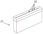
The structure may also at least partially surround a border structure of the area filled with said first building material. Fig. 2B illustrates a representative example of edge structures 66 formed by vector scanning in layer 60.
The structure may also be an interlayer connection structure. In these embodiments, the structure is preferably small (e.g., 1% smaller) relative to the overall layer. Fig. 2C illustrates a representative example of an interlayer structure 68 connecting two layers 60 and 70.
Structures may also be embedded in the area formed by the raster scan. For example, referring again to fig. 2A, main region 72 of layer 60 may be formed by raster scanning, wherein structures 62 may be embedded in region 72.
The structure may also be at the periphery of the layer. Fig. 2D illustrates this embodiment, in which layer 60 is shown with structure 74 at its periphery.
A combination of raster and vector scanning may be performed in any of the layers forming the object. In particular, in some embodiments a combination of raster and vector scanning is performed for inner layers of the plurality of layers, in some embodiments a combination of raster and vector scanning is performed for the uppermost layer, and in some embodiments a combination of raster and vector scanning is performed for the lowermost layer. A combination of raster and vector scanning may also be performed in multiple layers, as desired.
Referring now to fig. 3, fig. 3 is a schematic illustration of an article 80 according to some embodiments of the invention.
The article 80 generally includes a plurality of layers 60 (only one layer shown in the top view of fig. 3) made of electrically non-conductive material and fabricated via three-dimensional printing, wherein at least one of the layers includes a pattern 82 of conductive lines made of electrically conductive material. The pattern 82 may be deposited onto or embedded into a region 84 of non-conductive material. The article 80 may be manufactured by the system 10 and/or method described above.
According to some embodiments of the invention, article 80 is a circuit, e.g., a circuit board. Fig. 4 is a schematic diagram of an apparatus 90 that includes circuitry 80. The device 90 is typically, but not necessarily, a large-scale electronic device. Representative examples of devices suitable for the present invention include, but are not limited to, optoelectronic systems, display systems (e.g., active matrix display systems), projection display systems, sensors, identification tags, storage media, smart cards (e.g., microprocessor cards, cryptographic cards, ATM cards, customer identification module cards known as sim cards), and projection displays, batteries. The device 90 may also be an electronic component, such as a diode system or a transistor system.
In some embodiments, which post-deposition curable materials, such as UV curable materials, are applied and deposited from a particular dispenser. Furthermore, uncured material, such as electrolyte, is applied and deposited from other dispensers. In addition, materials that yield conductive materials after deposition are also used. All of the materials may be used together to construct a single device, e.g., a battery.
It is expected that during the life of a patent derived from this application, many relevant electronic devices (especially in the field of large-scale electronic devices) will be developed and the scope of the term "device" is intended to include all such new technologies a priori.
One or more operations of the method of an embodiment of the present invention are implemented by a computer. Computer program implemented methods embodying embodiments of the present invention are generally distributed to users of distribution media such as, but not limited to, floppy disks, CD-ROMs, flash memory devices, and portable hard disks. From the distribution medium, the computer program can be copied to a hard disk or similar intermediate storage device. The computer program may be run by loading computer instructions from its distribution medium or an intermediate storage device into the memory of an executing computer and configuring the computer to operate according to the method of the present invention. All of these operations are well known to those skilled in the art of computer systems.
The computer-implemented methods of embodiments of the present invention may be embodied in a variety of forms. For example, it may be embodied in tangible media, such as computers, for performing the method operations. May be embodied on a computer readable medium containing computer readable instructions for performing the operations of the method. It may also be embodied in an electronic device having the capabilities of a digital computer configured to run a computer program on a tangible medium or to execute instructions on a computer readable medium.
It is expected that during the life of a patent derived from this application, many relevant modeling materials for AM will be developed and the scope of the term "modeling material" is intended to include all such new technologies a priori.
For the purposes of this use, the term "about" means ± 10%.
The word "exemplary" is used herein to mean "serving as an example, instance, or illustration. Any embodiment described as "exemplary" is not necessarily to be construed as preferred or advantageous over other embodiments and/or to exclude the incorporation of features from other embodiments.
The word "selectively" is used herein to mean "configured in some embodiments but not in others". Any particular embodiment of the invention may incorporate a plurality of "optional" features, unless such features conflict.
The terms "comprising," including, "" containing, "" including, "" having, "and combinations thereof mean" including but not limited to.
The term "consisting of …" means "including and limited to".
The term "consisting essentially of …" means that an ingredient, method, or structure may include additional elements, steps, and/or components, but provides that the additional elements, steps, and/or components do not materially alter the basic novel characteristics of the claimed ingredient, method, or structure.
As used herein, the singular forms "a", "an" and "the" include plural referents unless the context clearly dictates otherwise. For example, the terms "a compound", "at least one", and "may include a plurality of compounds, including mixtures thereof.
Throughout this application, various embodiments of the invention may be presented in a range format. It is to be understood that the description in range format is merely for convenience and brevity and should not be construed as an inflexible limitation on the scope of the invention. Thus, the description of a range should be considered to have all the possible subranges specifically disclosed as well as individual numerical values within that range. For example, descriptions of ranges such as from 1 to 6 should be understood as having the specifically disclosed sub-ranges (e.g., from 1 to 3, from 1 to 4, from 1 to 5, from 2 to 4, from 2 to 6, from 3 to 6, etc.) as well as individual values within that range, e.g., 1, 2, 3, 4, 5, and 6. These are independent of the breadth of the range.
Whenever a range of values is expressed herein, it is meant to include any recited value (decimal or integer) within the range. The phrases "range within/between the first indicated value and the second indicated value" and "range" from the first indicated value "to the second indicated value are used interchangeably herein to mean including the first and second indicated values and all fractional or integer values therebetween.
It is appreciated that particular features of the invention, which are, for clarity, described in the context of separate embodiments, may also be provided in combination in a single embodiment. Conversely, various features of the invention, which are, for brevity, described in the context of a single embodiment, may also be provided separately or in any suitable subcombination or in any other embodiment described herein. Specific features described in the context of various embodiments are not considered essential features of those embodiments, unless the embodiments are inoperable without these elements.
While the invention has been described in conjunction with specific embodiments thereof, it is evident that many alternatives, modifications and variations will be apparent to those skilled in the art. Accordingly, it is intended to embrace all such alternatives, modifications and variations that fall within the spirit and broad scope of the appended claims.
All publications, patents and patent applications mentioned in this specification are herein incorporated in their entirety by reference into the specification, to the same extent as if each individual publication, patent or patent application was specifically and individually indicated to be incorporated herein by reference. In addition, citation or identification of any reference in this specification shall not be construed as an admission that such reference is available as prior art to the present invention. To the extent that paragraph headings are used, they should not be construed as necessarily limiting.
Claims (12)
1. A method of additive manufacturing of a three-dimensional object, the method comprising:
sequentially forming a plurality of layers, each patterned according to a shape of a cross section of the object, thereby forming the object;
wherein for at least one layer of the plurality of layers, the forming of the layer comprises dispensing at least a first building material composition at a first temperature and dispensing at least a second building material composition at a second temperature lower than the first temperature;
wherein the first temperature is greater than 60 ℃ and the second temperature is less than 40 ℃, wherein the second build material composition comprises a volatile solvent, and wherein the first build material composition is free of a volatile solvent.
2. The method of claim 1, wherein the first temperature is greater than 65 ℃.
3. A method according to one of claims 1 and 2, wherein said first building material composition is generally electrically non-conductive and said second building material is generally electrically conductive.
4. The method according to one of claims 1 and 2, wherein said dispensing said first building material composition is characterized by a raster scan.
5. The method according to one of claims 1 and 2, wherein said dispensing said second building material composition is characterized by a raster scan.
6. The method according to one of claims 1 and 2, wherein said dispensing said second building material composition is characterized by a vector scan.
7. The method of claim 6, wherein the vector scan is performed along a path selected to form at least one structure selected from the group consisting of: (i) an elongate structure, (ii) a border structure at least partially surrounding an area filled with the first build material, and (iii) an inter-layer connection structure.
8. The method according to one of claims 1 and 2, wherein at least one of said first building material composition and said second building material composition is UV cured.
9. The method according to one of claims 1 and 2, wherein said dispensing said first building material composition is performed by a first dispensing head and said dispensing said second building material composition is performed by a second dispensing head, and wherein said method comprises maintaining said first dispensing head and said second dispensing head at different temperatures.
10. The method of claim 9, wherein the maintaining the first and second dispense heads at different temperatures is performed by a controller of the same additive manufacturing system.
11. The method according to one of claims 1 and 2, wherein the dispensing the first build material composition is performed by a first dispensing head and the dispensing the second build material composition is performed by a second dispensing head, and wherein the method comprises:
the first temperature is controlled separately when the first building material composition is loaded to the first dispensing head and the second temperature is controlled separately when the second building material composition is loaded to the second dispensing head.
12. The method according to one of claims 1 and 2, wherein said dispensing said first building material composition is characterized by a raster scan and said dispensing said second building material composition is characterized by a vector scan.
Applications Claiming Priority (3)
| Application Number | Priority Date | Filing Date | Title |
|---|---|---|---|
| US201161476275P | 2011-04-17 | 2011-04-17 | |
| US61/476,275 | 2011-04-17 | ||
| CN201280023976.XA CN103747943B (en) | 2011-04-17 | 2012-04-17 | System and method for additive manufacturing of an object |
Related Parent Applications (1)
| Application Number | Title | Priority Date | Filing Date |
|---|---|---|---|
| CN201280023976.XA Division CN103747943B (en) | 2011-04-17 | 2012-04-17 | System and method for additive manufacturing of an object |
Publications (2)
| Publication Number | Publication Date |
|---|---|
| CN108058373A CN108058373A (en) | 2018-05-22 |
| CN108058373B true CN108058373B (en) | 2021-03-16 |
Family
ID=46172830
Family Applications (2)
| Application Number | Title | Priority Date | Filing Date |
|---|---|---|---|
| CN201280023976.XA Active CN103747943B (en) | 2011-04-17 | 2012-04-17 | System and method for additive manufacturing of an object |
| CN201710358660.0A Active CN108058373B (en) | 2011-04-17 | 2012-04-17 | System and method for additive manufacturing of objects |
Family Applications Before (1)
| Application Number | Title | Priority Date | Filing Date |
|---|---|---|---|
| CN201280023976.XA Active CN103747943B (en) | 2011-04-17 | 2012-04-17 | System and method for additive manufacturing of an object |
Country Status (8)
| Country | Link |
|---|---|
| US (5) | US9649811B2 (en) |
| EP (1) | EP2699406B1 (en) |
| JP (3) | JP6000334B2 (en) |
| CN (2) | CN103747943B (en) |
| ES (1) | ES2777174T3 (en) |
| HK (1) | HK1252019A1 (en) |
| IL (1) | IL228914B (en) |
| WO (1) | WO2012143923A2 (en) |
Families Citing this family (99)
| Publication number | Priority date | Publication date | Assignee | Title |
|---|---|---|---|---|
| US9649811B2 (en) | 2011-04-17 | 2017-05-16 | Stratasys Ltd. | System and method for additive manufacturing of an object |
| US9473760B2 (en) * | 2012-08-08 | 2016-10-18 | Makerbot Industries, Llc | Displays for three-dimensional printers |
| US9216544B2 (en) * | 2012-12-21 | 2015-12-22 | Stratasys, Inc. | Automated additive manufacturing system for printing three-dimensional parts, printing farm thereof, and method of use thereof |
| US8961167B2 (en) | 2012-12-21 | 2015-02-24 | Stratasys, Inc. | Automated additive manufacturing system for printing three-dimensional parts, printing farm thereof, and method of use thereof |
| WO2014200595A2 (en) * | 2013-03-15 | 2014-12-18 | 3D Systems, Inc. | Direct writing for additive manufacturing systems |
| US9533372B2 (en) | 2013-05-03 | 2017-01-03 | United Technologies Corporation | Method of eliminating sub-surface porosity |
| EP3013565B1 (en) * | 2013-06-24 | 2020-01-22 | President and Fellows of Harvard College | Printed three-dimensional (3d) functional part and method of making |
| JP6145333B2 (en) * | 2013-06-26 | 2017-06-07 | 矢崎総業株式会社 | Anticorrosion molding method |
| DE102013220578A1 (en) * | 2013-10-11 | 2015-04-16 | Arburg Gmbh + Co. Kg | Three-dimensional object with self-supporting wall |
| TW201522013A (en) * | 2013-12-12 | 2015-06-16 | 三緯國際立體列印科技股份有限公司 | Three dimensional printing apparatus |
| EP2887011B1 (en) | 2013-12-20 | 2017-02-08 | Hexagon Technology Center GmbH | Coordinate measuring machine with high precision 3D printing functionality |
| US9011136B1 (en) * | 2014-02-19 | 2015-04-21 | Massivit 3D Printing Technologies Ltd | Additive manufacturing device |
| JP6573903B2 (en) | 2014-03-25 | 2019-09-11 | ストラタシス リミテッド | Method and system for producing a layer crossing pattern |
| TWI491496B (en) * | 2014-05-08 | 2015-07-11 | 三緯國際立體列印科技股份有限公司 | Three dimensional printing apparatus, printing calibration board and three dimensional printing calibration method thereof |
| WO2015175651A1 (en) * | 2014-05-13 | 2015-11-19 | Massachusetts Institute Of Technology | Systems, devices, and methods for three-dimensional printing |
| DE102014007562B4 (en) * | 2014-05-22 | 2017-02-23 | Hendrik John | Process for the production of three-dimensional molded parts with integrated pattern structure by additive manufacturing |
| CN104461211B (en) * | 2014-05-31 | 2017-07-04 | 福州大学 | A kind of 3D manufacture methods of resistive touch screen |
| CN104411122B (en) * | 2014-05-31 | 2017-10-20 | 福州大学 | A kind of 3D printing method of multi-layer flexible circuit board |
| CN104407726B (en) * | 2014-05-31 | 2017-09-22 | 福州大学 | A kind of integrated touch function display screen and its manufacture method |
| CN104057611B (en) * | 2014-06-05 | 2016-03-23 | 浙江大学 | A kind of 3D optimized based on scan line inclination angle prints fill path generation method |
| US9833802B2 (en) * | 2014-06-27 | 2017-12-05 | Pulse Finland Oy | Methods and apparatus for conductive element deposition and formation |
| WO2016007672A1 (en) * | 2014-07-09 | 2016-01-14 | Applied Materials, Inc. | Layerwise heating, linewise heating, plasma heating and multiple feed materials in additive manufacturing |
| EP3524406B1 (en) | 2014-07-13 | 2021-03-03 | Stratasys Ltd. | Method and system for rotational 3d printing |
| US20160052056A1 (en) * | 2014-08-22 | 2016-02-25 | Arcam Ab | Enhanced electron beam generation |
| JP6396723B2 (en) * | 2014-08-25 | 2018-09-26 | 株式会社ミマキエンジニアリング | Droplet discharge apparatus and droplet discharge method |
| US9656428B2 (en) * | 2014-09-09 | 2017-05-23 | Disney Enterprises, Inc. | Three dimensional (3D) printed objects with embedded identification (ID) elements |
| US20160092041A1 (en) * | 2014-09-29 | 2016-03-31 | Madesolid, Inc. | System and method to facilitate material selection for a three dimensional printing object |
| CN110757796B (en) * | 2014-11-24 | 2022-10-11 | 添加剂工业有限公司 | Apparatus and method for producing an article by additive manufacturing |
| WO2016088048A1 (en) * | 2014-12-01 | 2016-06-09 | Sabic Global Technologies B.V. | Rapid nozzle cooling for additive manufacturing |
| FR3029838A1 (en) * | 2014-12-11 | 2016-06-17 | Centre Nat Rech Scient | METHOD FOR ADDITIVE MANUFACTURING OF A 3D MECATRONIC OBJECT |
| FR3030903B1 (en) * | 2014-12-18 | 2018-04-20 | Commissariat A L'energie Atomique Et Aux Energies Alternatives | METHOD FOR PRODUCING A RADIO FREQUENCY COMMUNICATION DEVICE |
| US9610733B2 (en) | 2015-01-06 | 2017-04-04 | Stratasys, Inc. | Additive manufacturing with soluble build sheet and part marking |
| JP6783784B2 (en) * | 2015-03-06 | 2020-11-11 | シグニファイ ホールディング ビー ヴィSignify Holding B.V. | 3D printing of (oxidized) graphene composite |
| WO2016146374A1 (en) * | 2015-03-17 | 2016-09-22 | Philips Lighting Holding B.V. | Making 3d printed shapes with interconnects and embedded components. |
| KR20170130515A (en) * | 2015-03-25 | 2017-11-28 | 스트라타시스 엘티디. | Method and system for sintering in-situ of conductive ink |
| WO2016171717A1 (en) * | 2015-04-24 | 2016-10-27 | Hewlett-Packard Development Company, L.P. | Three-dimensional object representation |
| CN105094088A (en) * | 2015-06-04 | 2015-11-25 | 周建钢 | Method and device for large-scale customerizing personalized products on assembly line |
| CN106273521A (en) * | 2015-06-05 | 2017-01-04 | 成都金采科技有限公司 | A kind of multiaxis multi-jet 3D printer |
| CN104943176B (en) * | 2015-06-23 | 2017-04-12 | 南京信息工程大学 | 3D printer based on image recognition technique and printing method of 3D printer |
| WO2017009830A1 (en) | 2015-07-13 | 2017-01-19 | Stratasys Ltd. | Operation of printing nozzles in additive manufacture and aparatus for cleaning printing nozzles |
| WO2017018985A1 (en) | 2015-07-24 | 2017-02-02 | Hewlett-Packard Development Company, L.P. | Three-dimensional (3d) printing |
| CN108025359B (en) * | 2015-07-24 | 2019-11-22 | 惠普发展公司,有限责任合伙企业 | Stabilisation liquid functional material for three-dimensional (3D) printing |
| EP3341868B1 (en) * | 2015-08-28 | 2022-11-30 | Materialise NV | Self supporting in additive manufacturing |
| WO2017035584A1 (en) * | 2015-08-31 | 2017-03-09 | LAZAREVIC, Steven | Reinforced additive manufacturing process for the manufacture of composite materials |
| FI129702B (en) | 2015-10-09 | 2022-07-15 | Inkron Ltd | Three dimensional printing materials and method for making a 3D printed article |
| JP6718132B2 (en) * | 2015-11-06 | 2020-07-08 | セイコーエプソン株式会社 | Method and apparatus for manufacturing three-dimensional structure |
| WO2017088134A1 (en) * | 2015-11-25 | 2017-06-01 | Siemens Product Lifecycle Management Software Inc. | System and method for modeling of parts with lattice structures |
| CN106926465A (en) * | 2015-12-31 | 2017-07-07 | 周宏志 | A kind of fractional scanning path generating method of control increasing material manufacturing stress deformation |
| JP6682878B2 (en) * | 2016-01-25 | 2020-04-15 | 富士ゼロックス株式会社 | Modeling equipment |
| CN105690764B (en) * | 2016-01-29 | 2017-09-01 | 北京工业大学 | Realize the ejecting device printed parallel and 3D printing method |
| WO2017142506A1 (en) * | 2016-02-15 | 2017-08-24 | Hewlett-Packard Development Company, L.P. | Build material supply for additive manufacturing |
| CN105657389B (en) * | 2016-03-22 | 2018-05-18 | 耿得力 | A kind of optical projection device and its calibration method |
| CN105881897B (en) * | 2016-03-30 | 2017-10-27 | 宁波大学 | The optimal mobile route planing method of shower nozzle in 3 D-printing |
| US10919228B2 (en) | 2016-04-04 | 2021-02-16 | Hewlett-Packard Development Company, L.P. | Definition of a shield feature for additive manufacture |
| EP3442781B1 (en) | 2016-04-15 | 2022-02-09 | Hewlett-Packard Development Company, L.P. | Material sets |
| KR101773717B1 (en) * | 2016-07-08 | 2017-08-31 | 국방과학연구소 | 3-D soft composite actuators priter |
| EP3909745A1 (en) | 2016-07-21 | 2021-11-17 | Hewlett-Packard Development Company, L.P. | Additively formed 3d object with conductive channel |
| DE102016213609A1 (en) * | 2016-07-25 | 2018-01-25 | Eos Gmbh Electro Optical Systems | Method and device for determining component quality |
| US20180065307A1 (en) * | 2016-09-06 | 2018-03-08 | Cc3D Llc | Systems and methods for controlling additive manufacturing |
| KR102142378B1 (en) * | 2016-10-17 | 2020-08-10 | 와커 헤미 아게 | Method for producing silicone elastomer products with improved print quality |
| KR102223983B1 (en) * | 2016-10-27 | 2021-03-08 | 휴렛-팩커드 디벨롭먼트 컴퍼니, 엘.피. | Additive Manufacturing Instruction Generation Technique |
| DE102016225289A1 (en) * | 2016-12-16 | 2018-06-21 | Koenig & Bauer Ag | Process for producing a structure on a carrier plate |
| DE102016225290A1 (en) * | 2016-12-16 | 2018-06-21 | Koenig & Bauer Ag | Process for producing a structure on a carrier plate |
| IT201600128438A1 (en) * | 2016-12-20 | 2018-06-20 | Gimac Di Maccagnan Giorgio | MANUFACTURING ADDITIVE PROCESS SYSTEM AND RELATED CONTROL METHOD |
| CN106493939B (en) * | 2016-12-22 | 2019-03-19 | 青岛理工大学 | The 3D printing method and 3D printer of embedded electronic product |
| US20180186073A1 (en) * | 2017-01-03 | 2018-07-05 | General Electric Company | Additive manufacturing systems including a particulate dispenser and methods of operating such systems |
| US10940638B2 (en) * | 2017-01-24 | 2021-03-09 | Continuous Composites Inc. | Additive manufacturing system having finish-follower |
| DE102017000744A1 (en) | 2017-01-27 | 2018-08-02 | Friedrich-Alexander-Universität Erlangen-Nürnberg | Method for producing an electronic or electrical system and system produced by the method |
| JP6868406B2 (en) * | 2017-01-31 | 2021-05-12 | 株式会社ミマキエンジニアリング | Three-dimensional object modeling device |
| CN106926452B (en) * | 2017-03-02 | 2019-05-21 | 西安交通大学 | A kind of multi-functional 3D printing head and its application method for material extrusion molding |
| CN106985390B (en) * | 2017-04-20 | 2019-01-01 | 南京师范大学 | A kind of devices and methods therefor based on three-dimensional printer printing machine winding |
| EP3615311A4 (en) * | 2017-04-26 | 2020-12-09 | Hewlett-Packard Development Company, L.P. | Printing conductive elements |
| RU177332U1 (en) * | 2017-05-31 | 2018-02-15 | Общество с ограниченной ответственностью "Центр аддитивных технологий" | 3D PRINTER BLOCK |
| BR112020001834A2 (en) | 2017-07-28 | 2020-07-28 | Hewlett-Packard Development Company, L.P. | modulation of a three-dimensional printer system based on a selected mode |
| CN111148483B (en) * | 2017-07-28 | 2022-11-15 | 斯特拉塔西斯公司 | Method and system for manufacturing an object with vascular properties |
| WO2019094280A1 (en) * | 2017-11-10 | 2019-05-16 | General Electric Company | Scan field variation for additive manufacturing |
| WO2019125488A1 (en) * | 2017-12-22 | 2019-06-27 | Hewlett-Packard Development Company, L.P. | Encoding in three-dimensional objects |
| EP3732015B1 (en) * | 2017-12-28 | 2023-11-08 | Stratasys Ltd. | Method and system for additive manufacturing of peelable sacrificial structure |
| US10595440B2 (en) | 2018-03-02 | 2020-03-17 | Northrop Grumman Systems Corporation | Thermal gasket with high transverse thermal conductivity |
| US11203156B2 (en) | 2018-08-20 | 2021-12-21 | NEXA3D Inc. | Methods and systems for photo-curing photo-sensitive material for printing and other applications |
| CN112955302B (en) * | 2018-09-28 | 2023-05-02 | 斯特拉塔西斯公司 | Method for manufacturing a laminate with partial curing |
| CN112930257B (en) | 2018-09-28 | 2023-03-24 | 斯特拉塔西斯公司 | Three-dimensional inkjet printing of thermally stable objects |
| IL282910B1 (en) | 2018-11-09 | 2024-04-01 | Nexa3D Inc | Three-dimensional printing system |
| WO2020132300A1 (en) * | 2018-12-20 | 2020-06-25 | Jabil Inc. | Apparatus, system and method of combining additive manufacturing print types |
| US11675853B2 (en) * | 2018-12-28 | 2023-06-13 | Nbcuniversal Media, Llc | Systems and methods for processing metadata |
| US11498283B2 (en) * | 2019-02-20 | 2022-11-15 | General Electric Company | Method and apparatus for build thickness control in additive manufacturing |
| EP3941714B1 (en) | 2019-03-18 | 2023-03-08 | Nexa3D Inc. | Method and system for additive manufacturing |
| US11040487B2 (en) * | 2019-03-27 | 2021-06-22 | Xerox Corporation | Method for operating an extruder in a three-dimensional (3D) object printer to improve layer formation |
| US10967573B2 (en) | 2019-04-02 | 2021-04-06 | NEXA3D Inc. | Tank assembly and components thereof for a 3D printing system |
| CN109986779B (en) * | 2019-04-09 | 2021-12-28 | 陈俊廷 | Additive manufacturing extrusion device of circuit board, additive manufacturing device using same and using method of additive manufacturing extrusion device |
| US20220040918A1 (en) * | 2019-04-29 | 2022-02-10 | Hewlett-Packard Development Company, L.P. | Three-dimensional printing |
| EP4242762A3 (en) * | 2019-05-17 | 2023-12-27 | Markforged, Inc. | 3d printing apparatus and method |
| CN112008976B (en) * | 2019-05-31 | 2023-01-31 | 西门子股份公司 | Additive manufacturing device and method |
| US20220113700A1 (en) * | 2019-06-26 | 2022-04-14 | Hewlett-Packard Development Company, L.P. | Geometrical transformations in additive manufacturing |
| CN111347674B (en) * | 2020-03-30 | 2022-11-22 | 上海市黄浦区劳动技术教育中心 | Electromagnetic matrix printer |
| IT202000007129A1 (en) * | 2020-04-03 | 2021-10-03 | Marco Zani | PROCESS OF REALIZATION OF AN OBJECT USING AN ADDITIVE MANUFACTURING DEVICE, ADDITIVE MANUFACTURING DEVICE AND CORRESPONDING IT PRODUCT |
| DE102021208882A1 (en) | 2021-08-13 | 2023-02-16 | Fraunhofer-Gesellschaft zur Förderung der angewandten Forschung eingetragener Verein | Device and method for forming functional elements on and/or in components |
| FR3141092A1 (en) * | 2022-10-20 | 2024-04-26 | Poietis | HANDLING AND TRANSFER OF OBJECTS BY PROPULSION |
| FR3141091A1 (en) * | 2022-10-20 | 2024-04-26 | Poietis | PRINTING OBJECTS FROM A WELL |
Citations (2)
| Publication number | Priority date | Publication date | Assignee | Title |
|---|---|---|---|---|
| TW511429B (en) * | 2000-05-25 | 2002-11-21 | Oak Mitsui Inc | Process to manufacture tight tolerance embedded elements for printed circuit boards |
| EP1360062A1 (en) * | 2001-02-15 | 2003-11-12 | Vantico Gmbh | Three-dimensional printing |
Family Cites Families (80)
| Publication number | Priority date | Publication date | Assignee | Title |
|---|---|---|---|---|
| US4764891A (en) * | 1985-03-18 | 1988-08-16 | Hughes Aircraft Company | Programmable methods of performing complex optical computations using data processing system |
| US4747069A (en) * | 1985-03-18 | 1988-05-24 | Hughes Aircraft Company | Programmable multistage lensless optical data processing system |
| US4944817A (en) * | 1986-10-17 | 1990-07-31 | Board Of Regents, The University Of Texas System | Multiple material systems for selective beam sintering |
| JP2658341B2 (en) * | 1989-01-13 | 1997-09-30 | 松下電器産業株式会社 | Thick film circuit forming equipment |
| JP2715527B2 (en) | 1989-03-14 | 1998-02-18 | ソニー株式会社 | 3D shape forming method |
| US5002855A (en) * | 1989-04-21 | 1991-03-26 | E. I. Du Pont De Nemours And Company | Solid imaging method using multiphasic photohardenable compositions |
| US6175422B1 (en) * | 1991-01-31 | 2001-01-16 | Texas Instruments Incorporated | Method and apparatus for the computer-controlled manufacture of three-dimensional objects from computer data |
| US6347257B1 (en) * | 1995-09-27 | 2002-02-12 | 3D Systems, Inc. | Method and apparatus for controlling the drop volume in a selective deposition modeling environment |
| US5943235A (en) * | 1995-09-27 | 1999-08-24 | 3D Systems, Inc. | Rapid prototyping system and method with support region data processing |
| CA2233225A1 (en) * | 1995-09-27 | 1997-04-03 | 3D Systems, Inc. | Selective deposition modeling method and apparatus for forming three-dimensional objects and supports |
| US6136252A (en) * | 1995-09-27 | 2000-10-24 | 3D Systems, Inc. | Apparatus for electro-chemical deposition with thermal anneal chamber |
| US6270335B2 (en) | 1995-09-27 | 2001-08-07 | 3D Systems, Inc. | Selective deposition modeling method and apparatus for forming three-dimensional objects and supports |
| US6596224B1 (en) * | 1996-05-24 | 2003-07-22 | Massachusetts Institute Of Technology | Jetting layers of powder and the formation of fine powder beds thereby |
| US6357855B1 (en) * | 1996-09-27 | 2002-03-19 | 3D Systems, Inc. | Non-linear printhead assembly |
| US5922364A (en) * | 1997-03-03 | 1999-07-13 | Young, Jr.; Albert C. | Stereolithography layering control system |
| JP4314414B2 (en) * | 1997-06-13 | 2009-08-19 | マサチューセッツ インスティテュート オブ テクノロジー | Powder jetting layer and formation of fine powder bed |
| US5902538A (en) * | 1997-08-29 | 1999-05-11 | 3D Systems, Inc. | Simplified stereolithographic object formation methods of overcoming minimum recoating depth limitations |
| DE69840914D1 (en) | 1997-10-14 | 2009-07-30 | Patterning Technologies Ltd | Method for producing an electrical capacitor |
| AU1818100A (en) * | 1998-11-12 | 2000-05-29 | Endale G. Haile-Mariam | Desktop projection monitor |
| US6399010B1 (en) * | 1999-02-08 | 2002-06-04 | 3D Systems, Inc. | Method and apparatus for stereolithographically forming three dimensional objects with reduced distortion |
| US6259962B1 (en) | 1999-03-01 | 2001-07-10 | Objet Geometries Ltd. | Apparatus and method for three dimensional model printing |
| US6658314B1 (en) | 1999-10-06 | 2003-12-02 | Objet Geometries Ltd. | System and method for three dimensional model printing |
| US6850334B1 (en) | 2000-01-18 | 2005-02-01 | Objet Geometries Ltd | System and method for three dimensional model printing |
| US6569373B2 (en) | 2000-03-13 | 2003-05-27 | Object Geometries Ltd. | Compositions and methods for use in three dimensional model printing |
| US20030207959A1 (en) | 2000-03-13 | 2003-11-06 | Eduardo Napadensky | Compositions and methods for use in three dimensional model printing |
| US7300619B2 (en) * | 2000-03-13 | 2007-11-27 | Objet Geometries Ltd. | Compositions and methods for use in three dimensional model printing |
| US6682684B1 (en) * | 2000-09-07 | 2004-01-27 | Honeywell International Inc. | Procedures for rapid build and improved surface characteristics in layered manufacture |
| GB0030095D0 (en) | 2000-12-09 | 2001-01-24 | Xaar Technology Ltd | Method of ink jet printing |
| US20020111707A1 (en) * | 2000-12-20 | 2002-08-15 | Zhimin Li | Droplet deposition method for rapid formation of 3-D objects from non-cross-linking reactive polymers |
| US20030151167A1 (en) * | 2002-01-03 | 2003-08-14 | Kritchman Eliahu M. | Device, system and method for accurate printing of three dimensional objects |
| JP3975272B2 (en) | 2002-02-21 | 2007-09-12 | 独立行政法人産業技術総合研究所 | Ultrafine fluid jet device |
| US6890050B2 (en) * | 2002-08-20 | 2005-05-10 | Palo Alto Research Center Incorporated | Method for the printing of homogeneous electronic material with a multi-ejector print head |
| AU2003286397A1 (en) | 2002-12-03 | 2004-06-23 | Objet Geometries Ltd. | Process of and apparatus for three-dimensional printing |
| AU2003900180A0 (en) * | 2003-01-16 | 2003-01-30 | Silverbrook Research Pty Ltd | Method and apparatus (dam001) |
| WO2004096527A2 (en) | 2003-05-01 | 2004-11-11 | Objet Geometries Ltd. | Rapid prototyping apparatus |
| JP2004358300A (en) * | 2003-06-02 | 2004-12-24 | Seiko Epson Corp | Apparatus and method for discharging liquid droplet, apparatus and method for manufacturing device, and electronic apparatus |
| US7108733B2 (en) * | 2003-06-20 | 2006-09-19 | Massachusetts Institute Of Technology | Metal slurry for electrode formation and production method of the same |
| JP2005183802A (en) * | 2003-12-22 | 2005-07-07 | Canon Inc | Electric circuit forming device |
| US20050263933A1 (en) * | 2004-05-28 | 2005-12-01 | 3D Systems, Inc. | Single side bi-directional feed for laser sintering |
| JP2006253255A (en) * | 2005-03-09 | 2006-09-21 | Seiko Epson Corp | Method of forming interconnection, and electronic device |
| US7658603B2 (en) * | 2005-03-31 | 2010-02-09 | Board Of Regents, The University Of Texas System | Methods and systems for integrating fluid dispensing technology with stereolithography |
| US7700016B2 (en) | 2005-08-02 | 2010-04-20 | Solidscape, Inc. | Method and apparatus for fabricating three dimensional models |
| JP3952480B2 (en) * | 2005-09-12 | 2007-08-01 | 三共化成株式会社 | Molded circuit component and manufacturing method thereof |
| US7555357B2 (en) * | 2006-01-31 | 2009-06-30 | Stratasys, Inc. | Method for building three-dimensional objects with extrusion-based layered deposition systems |
| WO2007114895A2 (en) * | 2006-04-06 | 2007-10-11 | Z Corporation | Production of three-dimensional objects by use of electromagnetic radiation |
| US20080006966A1 (en) * | 2006-07-07 | 2008-01-10 | Stratasys, Inc. | Method for building three-dimensional objects containing metal parts |
| JP2008098280A (en) * | 2006-10-10 | 2008-04-24 | Shinano Kenshi Co Ltd | Electronic component 3d molding device |
| CA2689675A1 (en) | 2007-02-07 | 2008-08-14 | Mcgill University | Bioceramic implants having bioactive substance |
| JP2008275970A (en) * | 2007-05-01 | 2008-11-13 | Seiko Epson Corp | Method for forming stereoscopic/variation image and ink jet device |
| JP2009006538A (en) * | 2007-06-27 | 2009-01-15 | Seiko Epson Corp | Three-dimensional shaping apparatus and method for three-dimenshional shaping |
| EP2664443B1 (en) * | 2007-07-25 | 2021-08-25 | Stratasys Ltd. | Solid freeform fabrication using a plurality of modeling materials |
| CN201077191Y (en) * | 2007-08-28 | 2008-06-25 | 杭州宏华数码科技股份有限公司 | Carpet decorating machine controlling movement and positioning of sprayer frame by gratings |
| JP2009124029A (en) * | 2007-11-16 | 2009-06-04 | Shinshu Univ | Method of manufacturing electronic circuit board using ink jetting |
| JP2009233573A (en) * | 2008-03-27 | 2009-10-15 | Seiko Epson Corp | Head unit, ejection apparatus, and ejection method |
| US20100021638A1 (en) | 2008-07-28 | 2010-01-28 | Solidscape, Inc. | Method for fabricating three dimensional models |
| US7962237B2 (en) | 2008-08-06 | 2011-06-14 | Objet Geometries Ltd. | Method and apparatus for optimizing a scanning plan in three-dimensional printing |
| JP2010118445A (en) * | 2008-11-12 | 2010-05-27 | Bridgestone Corp | Thin-film transistor, and method of manufacturing the same |
| JP5540575B2 (en) * | 2009-06-15 | 2014-07-02 | 日産自動車株式会社 | Current collector for bipolar secondary battery, bipolar secondary battery, assembled battery, vehicle, control device for bipolar secondary battery, and control method for bipolar secondary battery |
| US20100323102A1 (en) * | 2009-06-23 | 2010-12-23 | Xerox Corporation | System and Method for Preparing Conductive Structures Using Radiation Curable Phase Change Gel Inks |
| JP2011054620A (en) * | 2009-08-31 | 2011-03-17 | Murata Mfg Co Ltd | Method of manufacturing multilayer wiring board |
| CN102473503B (en) * | 2009-09-14 | 2014-11-05 | 米斯德国有限公司 | Method for producing an electric component and electric component |
| US8603612B2 (en) * | 2010-04-22 | 2013-12-10 | Xerox Corporation | Curable compositions for three-dimensional printing |
| EP2605898B1 (en) * | 2010-08-20 | 2020-09-30 | Zydex Pty Ltd | Apparatus and method for making an object |
| US9649811B2 (en) | 2011-04-17 | 2017-05-16 | Stratasys Ltd. | System and method for additive manufacturing of an object |
| US9776376B2 (en) * | 2011-08-29 | 2017-10-03 | Impossible Objects, LLC | Methods and apparatus for three-dimensional printed composites based on flattened substrate sheets |
| EP2914433B1 (en) * | 2012-11-05 | 2018-03-28 | Stratasys Ltd. | System and method for direct inkjet printing of 3d objects |
| CN105188993A (en) * | 2013-03-15 | 2015-12-23 | 麦特法布公司 | Cartridge for an additive manufacturing apparatus and method |
| TW201609934A (en) * | 2014-07-01 | 2016-03-16 | 精工愛普生股份有限公司 | Three-dimension formation composition, method of manufacturing three-dimensional structure, and three-dimensional structure |
| US11117291B2 (en) * | 2015-02-02 | 2021-09-14 | Massivit 3D Printing Technologies Ltd | Curing system for printing of 3D objects |
| JP6475328B2 (en) * | 2015-06-08 | 2019-02-27 | 富士フイルム株式会社 | Actinic ray curable inkjet ink set for 3D printing, 3D printing method, and 3D printing system |
| US20170291261A1 (en) * | 2015-06-12 | 2017-10-12 | Ashok Chand Mathur | Method And Apparatus Of Very Much Faster 3D Printer |
| WO2017009831A1 (en) * | 2015-07-13 | 2017-01-19 | Stratasys Ltd. | Method and system for 3d printing |
| US11059217B2 (en) * | 2015-11-23 | 2021-07-13 | Frank A. McKiel, Jr. | Method and apparatus for transposing extruded materials to fabricate an object surface |
| EP4215594A1 (en) * | 2016-04-07 | 2023-07-26 | 3D Systems, Incorporated | Thiol-ene inks for 3d printing |
| US10926454B2 (en) * | 2016-05-20 | 2021-02-23 | Sartorius Stedim Biotech Gmbh | Dispensing device and system for biological products |
| WO2017223379A1 (en) * | 2016-06-22 | 2017-12-28 | Service King Paint & Body, Llc | Automotive repair systems including handheld extruder |
| US11148358B2 (en) * | 2017-01-03 | 2021-10-19 | General Electric Company | Methods and systems for vacuum powder placement in additive manufacturing systems |
| US20180281283A1 (en) * | 2017-03-28 | 2018-10-04 | Velo3D, Inc. | Material manipulation in three-dimensional printing |
| US20180296343A1 (en) * | 2017-04-18 | 2018-10-18 | Warsaw Orthopedic, Inc. | 3-d printing of porous implants |
| US11660196B2 (en) * | 2017-04-21 | 2023-05-30 | Warsaw Orthopedic, Inc. | 3-D printing of bone grafts |
-
2012
- 2012-04-17 US US14/112,252 patent/US9649811B2/en active Active
- 2012-04-17 CN CN201280023976.XA patent/CN103747943B/en active Active
- 2012-04-17 CN CN201710358660.0A patent/CN108058373B/en active Active
- 2012-04-17 JP JP2014505781A patent/JP6000334B2/en active Active
- 2012-04-17 WO PCT/IL2012/050137 patent/WO2012143923A2/en active Application Filing
- 2012-04-17 EP EP12723927.5A patent/EP2699406B1/en active Active
- 2012-04-17 ES ES12723927T patent/ES2777174T3/en active Active
-
2013
- 2013-10-16 IL IL228914A patent/IL228914B/en active IP Right Grant
-
2016
- 2016-08-30 JP JP2016167978A patent/JP6317791B2/en active Active
-
2017
- 2017-04-24 US US15/494,577 patent/US10016937B2/en active Active
-
2018
- 2018-03-30 JP JP2018068439A patent/JP6626149B2/en active Active
- 2018-05-22 US US15/985,778 patent/US10406752B2/en active Active
- 2018-09-05 HK HK18111349.5A patent/HK1252019A1/en unknown
-
2019
- 2019-08-07 US US16/533,828 patent/US11254057B2/en active Active
-
2022
- 2022-02-10 US US17/668,435 patent/US11872766B2/en active Active
Patent Citations (2)
| Publication number | Priority date | Publication date | Assignee | Title |
|---|---|---|---|---|
| TW511429B (en) * | 2000-05-25 | 2002-11-21 | Oak Mitsui Inc | Process to manufacture tight tolerance embedded elements for printed circuit boards |
| EP1360062A1 (en) * | 2001-02-15 | 2003-11-12 | Vantico Gmbh | Three-dimensional printing |
Also Published As
| Publication number | Publication date |
|---|---|
| JP2014514193A (en) | 2014-06-19 |
| US11872766B2 (en) | 2024-01-16 |
| JP2018139292A (en) | 2018-09-06 |
| WO2012143923A2 (en) | 2012-10-26 |
| WO2012143923A3 (en) | 2013-03-28 |
| EP2699406B1 (en) | 2020-02-19 |
| IL228914B (en) | 2019-05-30 |
| US9649811B2 (en) | 2017-05-16 |
| US20140036455A1 (en) | 2014-02-06 |
| CN108058373A (en) | 2018-05-22 |
| US20190389133A1 (en) | 2019-12-26 |
| US20180264734A1 (en) | 2018-09-20 |
| US11254057B2 (en) | 2022-02-22 |
| JP2016221975A (en) | 2016-12-28 |
| HK1252019A1 (en) | 2019-05-10 |
| EP2699406A2 (en) | 2014-02-26 |
| JP6317791B2 (en) | 2018-04-25 |
| CN103747943B (en) | 2017-05-24 |
| JP6000334B2 (en) | 2016-09-28 |
| JP6626149B2 (en) | 2019-12-25 |
| US10406752B2 (en) | 2019-09-10 |
| US10016937B2 (en) | 2018-07-10 |
| US20220266523A1 (en) | 2022-08-25 |
| US20170225390A1 (en) | 2017-08-10 |
| IL228914A0 (en) | 2013-12-31 |
| ES2777174T3 (en) | 2020-08-04 |
| CN103747943A (en) | 2014-04-23 |
Similar Documents
| Publication | Publication Date | Title |
|---|---|---|
| CN108058373B (en) | System and method for additive manufacturing of objects | |
| US11904525B2 (en) | Method and system for fabricating cross-layer pattern | |
| US10688715B2 (en) | System and method for additive manufacturing of an object | |
| CN105939836B (en) | Building material profile | |
| TWI606915B (en) | 3D printing device with reciprocating spray forming mechanism | |
| CN107614265A (en) | The method and system of electrically conductive ink in-situ sintering | |
| WO2008120183A1 (en) | Method and system for three-dimensional fabrication | |
| US20180194070A1 (en) | 3d printing using preformed reuseable support structure |
Legal Events
| Date | Code | Title | Description |
|---|---|---|---|
| PB01 | Publication | ||
| PB01 | Publication | ||
| SE01 | Entry into force of request for substantive examination | ||
| SE01 | Entry into force of request for substantive examination | ||
| REG | Reference to a national code |
Ref country code: HK Ref legal event code: DE Ref document number: 1252019 Country of ref document: HK |
|
| GR01 | Patent grant | ||
| GR01 | Patent grant |