CN101852914A - Mems structures, methods of fabricating mems components on separate substrates and assembly of same - Google Patents
Mems structures, methods of fabricating mems components on separate substrates and assembly of same Download PDFInfo
- Publication number
- CN101852914A CN101852914A CN201010000258A CN201010000258A CN101852914A CN 101852914 A CN101852914 A CN 101852914A CN 201010000258 A CN201010000258 A CN 201010000258A CN 201010000258 A CN201010000258 A CN 201010000258A CN 101852914 A CN101852914 A CN 101852914A
- Authority
- CN
- China
- Prior art keywords
- substrate
- front substrate
- backboard
- movable electrode
- carrier
- Prior art date
- Legal status (The legal status is an assumption and is not a legal conclusion. Google has not performed a legal analysis and makes no representation as to the accuracy of the status listed.)
- Pending
Links
- 239000000758 substrate Substances 0.000 title claims abstract description 847
- 238000000034 method Methods 0.000 title claims abstract description 174
- 238000000151 deposition Methods 0.000 claims abstract description 58
- 230000008021 deposition Effects 0.000 claims abstract description 52
- 238000000059 patterning Methods 0.000 claims abstract description 49
- 238000004519 manufacturing process Methods 0.000 claims abstract description 42
- 239000000463 material Substances 0.000 claims description 199
- 230000003287 optical effect Effects 0.000 claims description 157
- 238000010276 construction Methods 0.000 claims description 82
- 230000003068 static effect Effects 0.000 claims description 68
- 239000000945 filler Substances 0.000 claims description 43
- 238000005516 engineering process Methods 0.000 claims description 38
- 230000008569 process Effects 0.000 claims description 34
- 238000001259 photo etching Methods 0.000 claims description 27
- 229910052751 metal Inorganic materials 0.000 claims description 23
- 239000002184 metal Substances 0.000 claims description 23
- 238000011049 filling Methods 0.000 claims description 11
- 208000002925 dental caries Diseases 0.000 claims description 5
- 239000003086 colorant Substances 0.000 claims description 2
- 238000005530 etching Methods 0.000 abstract description 43
- 238000004049 embossing Methods 0.000 abstract 1
- 238000010030 laminating Methods 0.000 abstract 1
- 238000007493 shaping process Methods 0.000 description 209
- 230000002093 peripheral effect Effects 0.000 description 50
- 239000007772 electrode material Substances 0.000 description 44
- 239000000565 sealant Substances 0.000 description 27
- 230000015572 biosynthetic process Effects 0.000 description 22
- 239000004020 conductor Substances 0.000 description 16
- 239000011521 glass Substances 0.000 description 14
- 238000003475 lamination Methods 0.000 description 14
- 230000008859 change Effects 0.000 description 12
- 238000013461 design Methods 0.000 description 12
- 230000000694 effects Effects 0.000 description 12
- 238000007789 sealing Methods 0.000 description 12
- 239000003989 dielectric material Substances 0.000 description 11
- 229920002120 photoresistant polymer Polymers 0.000 description 11
- 230000008901 benefit Effects 0.000 description 10
- 239000004568 cement Substances 0.000 description 10
- 230000000717 retained effect Effects 0.000 description 10
- 230000000007 visual effect Effects 0.000 description 10
- PNEYBMLMFCGWSK-UHFFFAOYSA-N Alumina Chemical compound [O-2].[O-2].[O-2].[Al+3].[Al+3] PNEYBMLMFCGWSK-UHFFFAOYSA-N 0.000 description 9
- VYPSYNLAJGMNEJ-UHFFFAOYSA-N Silicium dioxide Chemical compound O=[Si]=O VYPSYNLAJGMNEJ-UHFFFAOYSA-N 0.000 description 8
- 239000006096 absorbing agent Substances 0.000 description 8
- 238000009413 insulation Methods 0.000 description 8
- 238000003825 pressing Methods 0.000 description 8
- 239000003795 chemical substances by application Substances 0.000 description 7
- 239000011651 chromium Substances 0.000 description 7
- 238000009434 installation Methods 0.000 description 7
- 239000007769 metal material Substances 0.000 description 7
- KFZMGEQAYNKOFK-UHFFFAOYSA-N Isopropanol Chemical compound CC(C)O KFZMGEQAYNKOFK-UHFFFAOYSA-N 0.000 description 6
- ZOKXTWBITQBERF-UHFFFAOYSA-N Molybdenum Chemical compound [Mo] ZOKXTWBITQBERF-UHFFFAOYSA-N 0.000 description 6
- 239000011810 insulating material Substances 0.000 description 6
- 238000005304 joining Methods 0.000 description 6
- 229910052750 molybdenum Inorganic materials 0.000 description 6
- 239000011733 molybdenum Substances 0.000 description 6
- 239000000049 pigment Substances 0.000 description 6
- 229910052782 aluminium Inorganic materials 0.000 description 5
- 238000013459 approach Methods 0.000 description 5
- 239000002274 desiccant Substances 0.000 description 5
- 230000005611 electricity Effects 0.000 description 5
- 238000005538 encapsulation Methods 0.000 description 5
- 230000036961 partial effect Effects 0.000 description 5
- 239000002904 solvent Substances 0.000 description 5
- VYZAMTAEIAYCRO-UHFFFAOYSA-N Chromium Chemical compound [Cr] VYZAMTAEIAYCRO-UHFFFAOYSA-N 0.000 description 4
- 239000000956 alloy Substances 0.000 description 4
- 229910045601 alloy Inorganic materials 0.000 description 4
- 229910052804 chromium Inorganic materials 0.000 description 4
- 239000012530 fluid Substances 0.000 description 4
- 229910052737 gold Inorganic materials 0.000 description 4
- MRNHPUHPBOKKQT-UHFFFAOYSA-N indium;tin;hydrate Chemical compound O.[In].[Sn] MRNHPUHPBOKKQT-UHFFFAOYSA-N 0.000 description 4
- 239000007788 liquid Substances 0.000 description 4
- 239000011159 matrix material Substances 0.000 description 4
- 239000000203 mixture Substances 0.000 description 4
- 210000000056 organ Anatomy 0.000 description 4
- 229920001721 polyimide Polymers 0.000 description 4
- 230000000630 rising effect Effects 0.000 description 4
- 235000012239 silicon dioxide Nutrition 0.000 description 4
- 239000000377 silicon dioxide Substances 0.000 description 4
- YCKRFDGAMUMZLT-UHFFFAOYSA-N Fluorine atom Chemical compound [F] YCKRFDGAMUMZLT-UHFFFAOYSA-N 0.000 description 3
- 101100111302 Saccharomyces cerevisiae (strain ATCC 204508 / S288c) BCK1 gene Proteins 0.000 description 3
- 101100513485 Saccharomyces cerevisiae (strain ATCC 204508 / S288c) MKK2 gene Proteins 0.000 description 3
- 239000011358 absorbing material Substances 0.000 description 3
- 238000010521 absorption reaction Methods 0.000 description 3
- 239000004411 aluminium Substances 0.000 description 3
- XAGFODPZIPBFFR-UHFFFAOYSA-N aluminium Chemical compound [Al] XAGFODPZIPBFFR-UHFFFAOYSA-N 0.000 description 3
- 230000003321 amplification Effects 0.000 description 3
- 238000004380 ashing Methods 0.000 description 3
- 239000003990 capacitor Substances 0.000 description 3
- 230000001413 cellular effect Effects 0.000 description 3
- 229910052731 fluorine Inorganic materials 0.000 description 3
- 239000011737 fluorine Substances 0.000 description 3
- 229910010272 inorganic material Inorganic materials 0.000 description 3
- 239000011147 inorganic material Substances 0.000 description 3
- 239000012528 membrane Substances 0.000 description 3
- PXHVJJICTQNCMI-UHFFFAOYSA-N nickel Substances [Ni] PXHVJJICTQNCMI-UHFFFAOYSA-N 0.000 description 3
- 238000003199 nucleic acid amplification method Methods 0.000 description 3
- 239000002245 particle Substances 0.000 description 3
- 229920000642 polymer Polymers 0.000 description 3
- 238000006116 polymerization reaction Methods 0.000 description 3
- 229910052709 silver Inorganic materials 0.000 description 3
- 125000006850 spacer group Chemical group 0.000 description 3
- 239000000126 substance Substances 0.000 description 3
- CSCPPACGZOOCGX-UHFFFAOYSA-N Acetone Chemical compound CC(C)=O CSCPPACGZOOCGX-UHFFFAOYSA-N 0.000 description 2
- 101100311067 Caenorhabditis elegans ssp-11 gene Proteins 0.000 description 2
- QPLDLSVMHZLSFG-UHFFFAOYSA-N Copper oxide Chemical compound [Cu]=O QPLDLSVMHZLSFG-UHFFFAOYSA-N 0.000 description 2
- 239000004642 Polyimide Substances 0.000 description 2
- ATJFFYVFTNAWJD-UHFFFAOYSA-N Tin Chemical compound [Sn] ATJFFYVFTNAWJD-UHFFFAOYSA-N 0.000 description 2
- RTAQQCXQSZGOHL-UHFFFAOYSA-N Titanium Chemical compound [Ti] RTAQQCXQSZGOHL-UHFFFAOYSA-N 0.000 description 2
- 239000000853 adhesive Substances 0.000 description 2
- 230000001070 adhesive effect Effects 0.000 description 2
- 229910052787 antimony Inorganic materials 0.000 description 2
- WATWJIUSRGPENY-UHFFFAOYSA-N antimony atom Chemical compound [Sb] WATWJIUSRGPENY-UHFFFAOYSA-N 0.000 description 2
- 238000003491 array Methods 0.000 description 2
- 239000011324 bead Substances 0.000 description 2
- 230000005540 biological transmission Effects 0.000 description 2
- 230000000903 blocking effect Effects 0.000 description 2
- 239000000969 carrier Substances 0.000 description 2
- HGAZMNJKRQFZKS-UHFFFAOYSA-N chloroethene;ethenyl acetate Chemical compound ClC=C.CC(=O)OC=C HGAZMNJKRQFZKS-UHFFFAOYSA-N 0.000 description 2
- 239000013078 crystal Substances 0.000 description 2
- 238000001035 drying Methods 0.000 description 2
- 239000003822 epoxy resin Substances 0.000 description 2
- 238000001704 evaporation Methods 0.000 description 2
- 229910052732 germanium Inorganic materials 0.000 description 2
- GNPVGFCGXDBREM-UHFFFAOYSA-N germanium atom Chemical compound [Ge] GNPVGFCGXDBREM-UHFFFAOYSA-N 0.000 description 2
- 229910052738 indium Inorganic materials 0.000 description 2
- APFVFJFRJDLVQX-UHFFFAOYSA-N indium atom Chemical compound [In] APFVFJFRJDLVQX-UHFFFAOYSA-N 0.000 description 2
- 238000002955 isolation Methods 0.000 description 2
- 238000003754 machining Methods 0.000 description 2
- 230000000873 masking effect Effects 0.000 description 2
- 229910052759 nickel Inorganic materials 0.000 description 2
- 239000004033 plastic Substances 0.000 description 2
- 229920003023 plastic Polymers 0.000 description 2
- 229920000647 polyepoxide Polymers 0.000 description 2
- 238000007639 printing Methods 0.000 description 2
- 238000012545 processing Methods 0.000 description 2
- 239000004065 semiconductor Substances 0.000 description 2
- 238000000926 separation method Methods 0.000 description 2
- 238000004528 spin coating Methods 0.000 description 2
- 239000010936 titanium Substances 0.000 description 2
- 229910052719 titanium Inorganic materials 0.000 description 2
- 239000012780 transparent material Substances 0.000 description 2
- WFKWXMTUELFFGS-UHFFFAOYSA-N tungsten Chemical compound [W] WFKWXMTUELFFGS-UHFFFAOYSA-N 0.000 description 2
- 229910052721 tungsten Inorganic materials 0.000 description 2
- 239000010937 tungsten Substances 0.000 description 2
- 238000003466 welding Methods 0.000 description 2
- IUVCFHHAEHNCFT-INIZCTEOSA-N 2-[(1s)-1-[4-amino-3-(3-fluoro-4-propan-2-yloxyphenyl)pyrazolo[3,4-d]pyrimidin-1-yl]ethyl]-6-fluoro-3-(3-fluorophenyl)chromen-4-one Chemical compound C1=C(F)C(OC(C)C)=CC=C1C(C1=C(N)N=CN=C11)=NN1[C@@H](C)C1=C(C=2C=C(F)C=CC=2)C(=O)C2=CC(F)=CC=C2O1 IUVCFHHAEHNCFT-INIZCTEOSA-N 0.000 description 1
- IRLPACMLTUPBCL-KQYNXXCUSA-N 5'-adenylyl sulfate Chemical compound C1=NC=2C(N)=NC=NC=2N1[C@@H]1O[C@H](COP(O)(=O)OS(O)(=O)=O)[C@@H](O)[C@H]1O IRLPACMLTUPBCL-KQYNXXCUSA-N 0.000 description 1
- QTBSBXVTEAMEQO-UHFFFAOYSA-N Acetic acid Chemical compound CC(O)=O QTBSBXVTEAMEQO-UHFFFAOYSA-N 0.000 description 1
- OKTJSMMVPCPJKN-UHFFFAOYSA-N Carbon Chemical compound [C] OKTJSMMVPCPJKN-UHFFFAOYSA-N 0.000 description 1
- HBBGRARXTFLTSG-UHFFFAOYSA-N Lithium ion Chemical compound [Li+] HBBGRARXTFLTSG-UHFFFAOYSA-N 0.000 description 1
- GRYLNZFGIOXLOG-UHFFFAOYSA-N Nitric acid Chemical compound O[N+]([O-])=O GRYLNZFGIOXLOG-UHFFFAOYSA-N 0.000 description 1
- XUIMIQQOPSSXEZ-UHFFFAOYSA-N Silicon Chemical compound [Si] XUIMIQQOPSSXEZ-UHFFFAOYSA-N 0.000 description 1
- 229910010413 TiO 2 Inorganic materials 0.000 description 1
- 230000004913 activation Effects 0.000 description 1
- 239000005030 aluminium foil Substances 0.000 description 1
- 230000008485 antagonism Effects 0.000 description 1
- 230000000712 assembly Effects 0.000 description 1
- 238000000429 assembly Methods 0.000 description 1
- 230000006399 behavior Effects 0.000 description 1
- 238000005452 bending Methods 0.000 description 1
- OJIJEKBXJYRIBZ-UHFFFAOYSA-N cadmium nickel Chemical compound [Ni].[Cd] OJIJEKBXJYRIBZ-UHFFFAOYSA-N 0.000 description 1
- 229910052799 carbon Inorganic materials 0.000 description 1
- 239000006229 carbon black Substances 0.000 description 1
- 239000011248 coating agent Substances 0.000 description 1
- 238000000576 coating method Methods 0.000 description 1
- 230000003750 conditioning effect Effects 0.000 description 1
- 229910052802 copper Inorganic materials 0.000 description 1
- 230000007797 corrosion Effects 0.000 description 1
- 238000005260 corrosion Methods 0.000 description 1
- 229960004643 cupric oxide Drugs 0.000 description 1
- 238000000354 decomposition reaction Methods 0.000 description 1
- 230000000881 depressing effect Effects 0.000 description 1
- SWXVUIWOUIDPGS-UHFFFAOYSA-N diacetone alcohol Natural products CC(=O)CC(C)(C)O SWXVUIWOUIDPGS-UHFFFAOYSA-N 0.000 description 1
- 238000010586 diagram Methods 0.000 description 1
- 239000006185 dispersion Substances 0.000 description 1
- 239000000428 dust Substances 0.000 description 1
- 238000009713 electroplating Methods 0.000 description 1
- 230000008020 evaporation Effects 0.000 description 1
- 230000001747 exhibiting effect Effects 0.000 description 1
- 238000001914 filtration Methods 0.000 description 1
- 239000005357 flat glass Substances 0.000 description 1
- 230000004927 fusion Effects 0.000 description 1
- 239000007789 gas Substances 0.000 description 1
- 229910002804 graphite Inorganic materials 0.000 description 1
- 239000010439 graphite Substances 0.000 description 1
- 238000010438 heat treatment Methods 0.000 description 1
- 230000006872 improvement Effects 0.000 description 1
- 239000012774 insulation material Substances 0.000 description 1
- 230000010354 integration Effects 0.000 description 1
- 229910001416 lithium ion Inorganic materials 0.000 description 1
- 239000003550 marker Substances 0.000 description 1
- XZWYZXLIPXDOLR-UHFFFAOYSA-N metformin Chemical compound CN(C)C(=N)NC(N)=N XZWYZXLIPXDOLR-UHFFFAOYSA-N 0.000 description 1
- 230000004048 modification Effects 0.000 description 1
- 238000012986 modification Methods 0.000 description 1
- 238000000465 moulding Methods 0.000 description 1
- 229910017604 nitric acid Inorganic materials 0.000 description 1
- 150000004767 nitrides Chemical class 0.000 description 1
- 229910052755 nonmetal Inorganic materials 0.000 description 1
- 238000005457 optimization Methods 0.000 description 1
- 239000011368 organic material Substances 0.000 description 1
- 239000003960 organic solvent Substances 0.000 description 1
- 229910052760 oxygen Inorganic materials 0.000 description 1
- 239000001301 oxygen Substances 0.000 description 1
- 238000005240 physical vapour deposition Methods 0.000 description 1
- 229910052697 platinum Inorganic materials 0.000 description 1
- 229920003229 poly(methyl methacrylate) Polymers 0.000 description 1
- 239000004417 polycarbonate Substances 0.000 description 1
- 229920000515 polycarbonate Polymers 0.000 description 1
- -1 polyethylene terephthalate Polymers 0.000 description 1
- 229920000139 polyethylene terephthalate Polymers 0.000 description 1
- 239000005020 polyethylene terephthalate Substances 0.000 description 1
- 239000004926 polymethyl methacrylate Substances 0.000 description 1
- 230000002829 reductive effect Effects 0.000 description 1
- 230000001172 regenerating effect Effects 0.000 description 1
- 230000001105 regulatory effect Effects 0.000 description 1
- 230000003014 reinforcing effect Effects 0.000 description 1
- 230000002040 relaxant effect Effects 0.000 description 1
- 239000005060 rubber Substances 0.000 description 1
- 229910052710 silicon Inorganic materials 0.000 description 1
- 239000010703 silicon Substances 0.000 description 1
- 239000011343 solid material Substances 0.000 description 1
- 238000009987 spinning Methods 0.000 description 1
- 238000005507 spraying Methods 0.000 description 1
- 238000004544 sputter deposition Methods 0.000 description 1
- 239000010935 stainless steel Substances 0.000 description 1
- 229910001220 stainless steel Inorganic materials 0.000 description 1
- 238000003860 storage Methods 0.000 description 1
- 239000000725 suspension Substances 0.000 description 1
- 230000002459 sustained effect Effects 0.000 description 1
- 229920001187 thermosetting polymer Polymers 0.000 description 1
- 239000004634 thermosetting polymer Substances 0.000 description 1
- 238000012546 transfer Methods 0.000 description 1
- 238000007666 vacuum forming Methods 0.000 description 1
- 238000005406 washing Methods 0.000 description 1
Images


Classifications
-
- G—PHYSICS
- G02—OPTICS
- G02B—OPTICAL ELEMENTS, SYSTEMS OR APPARATUS
- G02B26/00—Optical devices or arrangements for the control of light using movable or deformable optical elements
-
- G—PHYSICS
- G02—OPTICS
- G02B—OPTICAL ELEMENTS, SYSTEMS OR APPARATUS
- G02B26/00—Optical devices or arrangements for the control of light using movable or deformable optical elements
- G02B26/08—Optical devices or arrangements for the control of light using movable or deformable optical elements for controlling the direction of light
- G02B26/0816—Optical devices or arrangements for the control of light using movable or deformable optical elements for controlling the direction of light by means of one or more reflecting elements
- G02B26/0833—Optical devices or arrangements for the control of light using movable or deformable optical elements for controlling the direction of light by means of one or more reflecting elements the reflecting element being a micromechanical device, e.g. a MEMS mirror, DMD
- G02B26/0841—Optical devices or arrangements for the control of light using movable or deformable optical elements for controlling the direction of light by means of one or more reflecting elements the reflecting element being a micromechanical device, e.g. a MEMS mirror, DMD the reflecting element being moved or deformed by electrostatic means
-
- B—PERFORMING OPERATIONS; TRANSPORTING
- B81—MICROSTRUCTURAL TECHNOLOGY
- B81B—MICROSTRUCTURAL DEVICES OR SYSTEMS, e.g. MICROMECHANICAL DEVICES
- B81B3/00—Devices comprising flexible or deformable elements, e.g. comprising elastic tongues or membranes
- B81B3/0064—Constitution or structural means for improving or controlling the physical properties of a device
- B81B3/0067—Mechanical properties
- B81B3/007—For controlling stiffness, e.g. ribs
-
- B—PERFORMING OPERATIONS; TRANSPORTING
- B81—MICROSTRUCTURAL TECHNOLOGY
- B81B—MICROSTRUCTURAL DEVICES OR SYSTEMS, e.g. MICROMECHANICAL DEVICES
- B81B7/00—Microstructural systems; Auxiliary parts of microstructural devices or systems
-
- G—PHYSICS
- G02—OPTICS
- G02B—OPTICAL ELEMENTS, SYSTEMS OR APPARATUS
- G02B26/00—Optical devices or arrangements for the control of light using movable or deformable optical elements
- G02B26/001—Optical devices or arrangements for the control of light using movable or deformable optical elements based on interference in an adjustable optical cavity
-
- G—PHYSICS
- G02—OPTICS
- G02B—OPTICAL ELEMENTS, SYSTEMS OR APPARATUS
- G02B5/00—Optical elements other than lenses
- G02B5/20—Filters
- G02B5/28—Interference filters
- G02B5/284—Interference filters of etalon type comprising a resonant cavity other than a thin solid film, e.g. gas, air, solid plates
-
- B—PERFORMING OPERATIONS; TRANSPORTING
- B81—MICROSTRUCTURAL TECHNOLOGY
- B81B—MICROSTRUCTURAL DEVICES OR SYSTEMS, e.g. MICROMECHANICAL DEVICES
- B81B2201/00—Specific applications of microelectromechanical systems
- B81B2201/04—Optical MEMS
- B81B2201/042—Micromirrors, not used as optical switches
-
- B—PERFORMING OPERATIONS; TRANSPORTING
- B81—MICROSTRUCTURAL TECHNOLOGY
- B81B—MICROSTRUCTURAL DEVICES OR SYSTEMS, e.g. MICROMECHANICAL DEVICES
- B81B2207/00—Microstructural systems or auxiliary parts thereof
- B81B2207/07—Interconnects
-
- B—PERFORMING OPERATIONS; TRANSPORTING
- B81—MICROSTRUCTURAL TECHNOLOGY
- B81B—MICROSTRUCTURAL DEVICES OR SYSTEMS, e.g. MICROMECHANICAL DEVICES
- B81B2207/00—Microstructural systems or auxiliary parts thereof
- B81B2207/09—Packages
- B81B2207/091—Arrangements for connecting external electrical signals to mechanical structures inside the package
- B81B2207/092—Buried interconnects in the substrate or in the lid
-
- H—ELECTRICITY
- H01—ELECTRIC ELEMENTS
- H01L—SEMICONDUCTOR DEVICES NOT COVERED BY CLASS H10
- H01L31/00—Semiconductor devices sensitive to infrared radiation, light, electromagnetic radiation of shorter wavelength or corpuscular radiation and specially adapted either for the conversion of the energy of such radiation into electrical energy or for the control of electrical energy by such radiation; Processes or apparatus specially adapted for the manufacture or treatment thereof or of parts thereof; Details thereof
- H01L31/04—Semiconductor devices sensitive to infrared radiation, light, electromagnetic radiation of shorter wavelength or corpuscular radiation and specially adapted either for the conversion of the energy of such radiation into electrical energy or for the control of electrical energy by such radiation; Processes or apparatus specially adapted for the manufacture or treatment thereof or of parts thereof; Details thereof adapted as photovoltaic [PV] conversion devices
-
- Y—GENERAL TAGGING OF NEW TECHNOLOGICAL DEVELOPMENTS; GENERAL TAGGING OF CROSS-SECTIONAL TECHNOLOGIES SPANNING OVER SEVERAL SECTIONS OF THE IPC; TECHNICAL SUBJECTS COVERED BY FORMER USPC CROSS-REFERENCE ART COLLECTIONS [XRACs] AND DIGESTS
- Y10—TECHNICAL SUBJECTS COVERED BY FORMER USPC
- Y10T—TECHNICAL SUBJECTS COVERED BY FORMER US CLASSIFICATION
- Y10T29/00—Metal working
- Y10T29/49—Method of mechanical manufacture
- Y10T29/49002—Electrical device making
- Y10T29/49117—Conductor or circuit manufacturing
- Y10T29/49124—On flat or curved insulated base, e.g., printed circuit, etc.
- Y10T29/49126—Assembling bases
Landscapes
- Physics & Mathematics (AREA)
- General Physics & Mathematics (AREA)
- Optics & Photonics (AREA)
- Engineering & Computer Science (AREA)
- Spectroscopy & Molecular Physics (AREA)
- Computer Hardware Design (AREA)
- Microelectronics & Electronic Packaging (AREA)
- Mechanical Engineering (AREA)
- Mechanical Light Control Or Optical Switches (AREA)
- Micromachines (AREA)
- Devices For Indicating Variable Information By Combining Individual Elements (AREA)
Abstract
Methods of fabricating a microelectromechanical systems (MEMS) device having elevated land regions for routing and MEMS devices formed by the same are disclosed. In one embodiment, an MEMS device is fabricated by laminating a front substrate and a carrier, each of which has components preformed thereon. Each of the front substrate and the carrier has a unit preformed thereon and has a cavity with a selected depth for interference modulation. Features are formed by deposition and patterning, by embossing, or by patterning and etching. The methods notonly reduce the manufacturing costs, but also provide a higher yield.
Description
Divide an application
Patented claim of the present invention is that application number is PCT/US2008/061812, the applying date is on April 28th, 2008, priority date is on May 11st, 2007, denomination of invention is that the PCT application of " mems structure; make the method and the subassembly thereof of MEMS (micro electro mechanical system) assembly on independent substrate " enters the China national stage, and application number is dividing an application of 200880015637.0 application for a patent for invention.
The cross reference of related application
The application's case is advocated the senior interest of the 60/917th, No. 609 provisional application case of application on May 11st, 2007 according to 35U.S.C. § 119 (e).Whole disclosure of this priority application case are incorporated herein by reference.The application's case is relevant for 2006/0067646A1 number (attorney docket IRDM.093A) U.S. Patent Application Publication case of " being manufactured in the MEMS devices (MEMS DEVICEFABRICATED ON A PRE-PATTERNED SUBSTRATE) on the pre-patterned substrate " with title.
Technical field
The present invention relates to microelectromechanicdevices devices and manufacture method thereof.More particularly, the present invention relates to interferometric modulator and manufacture method thereof.
Background technology
MEMS (micro electro mechanical system) (MEMS) comprises micromechanical component, actuator and electron device.Can use deposition, etching and/or etch away substrate and/or a plurality of parts of institute's deposited material layer or add layer and produce micromechanical component with other micromachined technology that forms electricity and electromechanical assembly.One type MEMS device is called as interferometric modulator.When being used for herein, term interferometric modulator or interferometric light modulator refer to uses principle of optical interference optionally to absorb and/or catoptrical device.In certain embodiments, interferometric modulator can comprise the pair of conductive plate, and wherein one or both can completely or partially be transparent and/or reflection, and can carry out relative motion after suitably electric signal applies.In a particular embodiment, a plate can comprise the quiescent layer that is deposited on the substrate, and another plate can comprise the metallic membrane that separates by air gap and quiescent layer.As describing in more detail herein, plate can change the optical interference that is incident on the light on the interferometric modulator with respect to the position of another plate.The application that these a little devices have broad range, and will be useful in this technology be to utilize and/or revise the characteristic of the device of these types, make that its feature can be in order to improvement existing product and the still undeveloped new product of generation.
Summary of the invention
The invention provides the method for making MEMS (micro electro mechanical system) (MEMS) device and the MEMS device that forms by described method.In one aspect, make the MEMS device by attached front substrate and carrier, each in front substrate and the carrier has preformed feature thereon.Can form feature by deposition and patterning or pass through to be shaped (for example, impression, patterning and etching or stamp).By being shaped and deposition is forming among some embodiment of feature, using a plurality of levels and do not use independent shade to form a plurality of patterns.The method of the routing infrastructure that is formed for the MEMS device is provided in another aspect.In aspect another, the MEMS device possesses spacer structure to keep the interval between front substrate and the backboard.In another aspect, be provided for forming black mask to prevent the method for unwanted reflection in the optical MEMS (for example, interferometric modulator).Method as described above not only reduces manufacturing cost, and but also provides higher yield.Gained MEMS device is difficult for being stressed and changes and the moisture leakage contribution.
On the one hand, provide a kind of method of the MEMS of manufacturing device.Described method comprises: provide the transparency electrode subassembly, the electrode that it comprises transparent substrates and is formed at the partially transparent at least on the described transparent substrates; Carrier is provided, and described carrier comprises reflecting electrode formed thereon; And described transparency electrode subassembly is attached to carrier, make described reflecting electrode towards the electrode of described partially transparent at least to form cavity.
In another aspect, provide a kind of method of making the interferometric device array.Described method comprises provides front substrate, and described front substrate comprises the support member that defines the cavity on the front substrate.Front substrate further comprises the front electrode that is formed in the described cavity.Described method further comprises: carrier is provided, and described carrier comprises movable electrode formed thereon; And front substrate is attached to carrier, make movable electrode towards at least a portion of front electrode to form one or more interferometric device.
In aspect another, provide a kind of MEMS (micro electro mechanical system) (MEMS) device.Described device comprises: front substrate, and it comprises a plurality of support members of the cavity that defines on the described front substrate; And by a plurality of movable electrodes of described supports support.In the described movable electrode each comprises the first that overlays on the support member and in abutting connection with the second portion of first.Described second portion overlays on the support member on not.First has first thickness.Second portion has second thickness.Second thickness is greater than first thickness.
In aspect another, provide a kind of MEMS (micro electro mechanical system) (MEMS) apparatus array.Described array comprises front substrate, and it comprises a plurality of support members of the cavity that defines on the described front substrate, and each in the wherein said cavity has basal surface.Described device further comprise relative with front substrate substantially and on overlay on backboard on the front substrate.Described backboard has towards the surface of the cavity of front substrate.Described surface lies front substrate farthest.Described device also comprises a plurality of mechanical band between the surface of inserting support member and backboard.In the described mechanical band each is served as the traveling electrode that is used for a plurality of MEMS devices.Distance between the basal surface of one in the cavity and the distal most surface of backboard is about 6,500
 And between about 20 μ m.
In another aspect, provide a kind of MEMS (micro electro mechanical system) (MEMS) device.Described device comprises: substrate, described substrate comprise with substrate is whole and forming and by a plurality of support members that form with the substrate identical materials; And a plurality of mechanical organs, it defines traveling electrode.Described mechanical organ is supported on the top of described support member.
In another aspect, provide a kind of MEMS (micro electro mechanical system) (MEMS) device.Described device comprises the substrate with surface.Described substrate comprises a plurality of grooves that form in the described surface of arrival.Described groove is parallel to each other substantially and extend.The upper zone of the delimited substrate of substrate, and groove defines the lower region of substrate.Described device further comprises a plurality of fixed electordes on the lower region that is formed at substrate.
In aspect another, provide a kind of front substrate that is used for MEMS (micro electro mechanical system) (MEMS).Described front substrate comprises substrate, and it comprises a plurality of support members of a plurality of cavitys that define on the described substrate.Described support member and substrate be whole to be formed and by forming with the substrate identical materials.Described front substrate further comprises the conductive layer in the cavity that is formed between the support member.
In another aspect, provide a kind of method of making interferometric modulator.Described method comprises from substrate and forms a plurality of support members.Described support member and substrate be whole to be formed and by forming with the substrate identical materials.Described method further comprises a plurality of mechanical organs that traveling electrode is defined in formation, makes described mechanical organ be supported on the support member.
The method of a kind of manufacturing MEMS (micro electro mechanical system) (MEMS) is provided in another aspect.Described method comprises: planar substrate is provided; And formation and described substrate be the supporting construction of integral type, to define the height of MEMS cavity.The MEMS cavity has the bottom surface, and the MEMS cavity is configured to hold therein the motion of traveling electrode.Described method further is included on the bottom surface of cavity and forms conductive layer.
In another aspect, provide a kind of MEMS (micro electro mechanical system) (MEMS) device.Described device comprises: front substrate, and it comprises a plurality of electrodes that are formed on the described front substrate; And carrier, it is relative with front substrate substantially, makes electrode insert between carrier and the front substrate.Described carrier comprises a plurality of tracks that extend from carrier.Device further comprises a plurality of movable electrodes between the track that inserts front substrate and carrier.
In another aspect, provide a kind of carrier that is formed with MEMS (micro electro mechanical system) (MEMS) front substrate of stationary electrode above being used to be attached to.Described carrier comprises the substrate that comprises a plurality of tracks.Described track defines the groove that replaces with described track.Carrier also comprises electrode layer, and described electrode layer comprises and is formed at the first on the track and is formed at second portion in the groove.Electrode layer is discontinuous between groove and track.
In aspect another, provide the method for a kind of manufacturing MEMS (micro electro mechanical system) (MEMS) array.Described MEMS array comprises the front substrate with first surface.Described front substrate comprises a plurality of fixedly lower electrodes that are formed on the described first surface.Described method comprises is shaped to have from the integrally formed boss of described carrier substrates carrier substrates.Described boss defines the groove that replaces with described boss.Described method further is included on the boss of carrier substrates and deposition mechanical layer in the groove.Described mechanical layer is discontinuous between groove and boss.
In another aspect, provide a kind of MEMS (micro electro mechanical system) (MEMS) device.Described device comprises: front substrate, and it comprises first support member that extends from described front substrate; Backboard, it has substantially and the front substrate facing surfaces, makes described first support member insert between the surface of front substrate and backboard; And traveling electrode, it inserts between front substrate and the backboard.Traveling electrode comprises the part that is supported on first support member.Described device further comprises second support member, its one extending from the surface of first support member of front substrate and backboard.Second support member is positioned between the surface of first support member of front substrate and backboard.
In another aspect, provide a kind of MEMS (micro electro mechanical system) (MEMS) device.Described device comprises the front substrate with first surface.Described front substrate comprises the Optical stack that is formed on the described first surface.Described device also comprises the backboard relative with front substrate.Described backboard has the second surface towards first surface.Backboard comprises from second surface towards first surface the pillar that extends, and makes the height of pillar define the distance between first surface and the second surface.Described device further comprises a plurality of movable electrode bands, and it is parallel to each other substantially and extend.Described band inserts between first surface and the second surface.
In aspect another, provide a kind of MEMS (micro electro mechanical system) (MEMS) device.Described device comprises front substrate and the backboard relative with described front substrate.Described backboard has the surface towards front substrate.Described device also comprises a plurality of movable electrode bands, and it is parallel to each other substantially and extend.Described band inserts between front substrate and the backboard.A plurality of parts of described band can move towards anterior substrate.Described device further comprises a plurality of pillars, and extend on its surface from backboard, makes described pillar through arranging described part the moving towards described surface with the restriction band.
The method of a kind of manufacturing MEMS (micro electro mechanical system) (MEMS) device is provided in another aspect.Described method comprises: front substrate is provided, and described front substrate comprises first support member that extends from front substrate; Backboard with surface is provided; Front substrate is attached to backboard, the support member of winning is inserted between the surface of front substrate and backboard; And forwardly form second support member between the surface of first support member of substrate and backboard, make described second support member extending from the surface of first support member of front substrate and backboard.
In another aspect, provide a kind of MEMS (micro electro mechanical system) (MEMS) device.Described device comprises the front substrate with first surface.Described front substrate comprises array region and the outer peripheral areas that is positioned on the described first surface.Described device also comprises backboard, and it has the second surface towards first surface.Has the gap between first surface and the second surface.Backboard comprises array region and the outer peripheral areas that is positioned on the second surface.Described device further comprises: conductor wire, and it forwardly extends on the outer peripheral areas of substrate; And conductive structure, it forwardly extends between the outer peripheral areas of the outer peripheral areas of substrate and backboard.Conductive structure contact conductor wire.
In another aspect, provide a kind of vehicle group component that is used to make interferometric modulator.Described interferometric modulator comprises front substrate, and described front substrate comprises transparent substantially electrode formed thereon.Described vehicle group component comprises: but releasing structure, and it has the surface; And a plurality of elongated conduction bands, it is formed on the described surface.Described elongated conduction band is parallel to each other substantially and extend in one direction.
In another aspect, provide a kind of interferometric modulator.Described interferometric modulator comprises the vehicle group component, and described vehicle group component comprises: but releasing structure, and it has the surface; And a plurality of elongated conduction bands, it is formed on the described surface.Described elongated conduction band is parallel to each other substantially and extend in one direction.Described interferometric modulator also comprises front substrate, and it comprises a plurality of support members and transparent substantially electrode.Front substrate is attached to the vehicle group component, makes the conduction band by supports support.
In aspect another, provide a kind of method of making interferometric modulator.Described interferometric modulator comprises front substrate, and described front substrate comprises a plurality of support members of the cavity that defines on the front substrate.Front substrate further comprises the lower electrode that is formed in the cavity.Described method comprises: but the releasing structure with surface is provided; Deposition movable electrode material on described surface; On described movable electrode material, provide shade, so that optionally expose the part of movable electrode material; And use optionally etching movable electrode material of described shade, thereby form a plurality of movable electrode bands.Described movable electrode band is parallel to each other substantially and extend in one direction.Described method further comprises but releasing structure is positioned on the front substrate, makes the cavity of movable electrode band towards front substrate.
In another aspect, provide a kind of MEMS (micro electro mechanical system) (MEMS) device.Described device comprises front substrate, and it comprises array region and outer peripheral areas.Described front substrate comprises a plurality of support members that are arranged in array region, defines a plurality of lower regions between described a plurality of support members.Front substrate further comprises the terminal pad that is arranged in outer peripheral areas.At least a portion of described terminal pad have with array region in the identical substantially height of support member.Described device also comprises a plurality of conductors on the terminal pad that is formed in the outer peripheral areas.Described conductor is electrically isolated from one.Described device further comprises the conductive layer on the lower region that is formed at front substrate.
In another aspect, provide a kind of carrier that is used for the combination of the front substrate of interferometric modulator.Described front substrate comprises transparent substantially electrode formed thereon.Described carrier comprises: substrate, and it comprises array region and outer peripheral areas; And a plurality of movable electrode bands, it is formed on the array region of substrate.Described band is parallel to each other substantially and extend.Described carrier further comprises a plurality of route traces that are formed on the described substrate.In the described trace each corresponding one extends to outer peripheral areas from described band.
In aspect another, provide a kind of MEMS (micro electro mechanical system) (MEMS) device.Described device comprises front substrate, and described front substrate comprises array region and outer peripheral areas.Front substrate comprises parallel to each other and a plurality of tracks of extending in the array region.Described track defines a plurality of grooves in the array region.Front substrate further comprises the groove in the outer peripheral areas.The corresponding extensions of in the described groove each from described groove.Described device further comprises the walking along the street that is formed in the groove by trace.Described walking along the street is extended at least a portion of outer peripheral areas by the groove of trace from array region.Walking along the street is electrically isolated from one by trace.
In another aspect, provide a kind of MEMS (micro electro mechanical system) (MEMS) device.Described device comprises front substrate, and described front substrate has and comprises array region and around the surface of the outer peripheral areas of described array region.Front substrate comprises the lip-deep annular seal zones that is positioned at front substrate.Described sealing area is substantially around array region.Sealing area has at upwardly extending first width towards the side of array region.Front substrate also comprises the dimple that forms in the arrival substrate.Described dimple has upwardly extending second width described side.Described second width is greater than described first width.Dimple extends across the part of described sealing area.Dimple defines the height lower than the height on the surface of front substrate.Front substrate further comprises: first conductive layer, and it is formed on the surface of front substrate; And second conductive layer, it is formed in the dimple, and wherein said first conductive layer and described second conductive layer are discontinuous each other.
The method of a kind of manufacturing MEMS (micro electro mechanical system) (MEMS) device is provided in another aspect.Described method comprises: front substrate is provided, and it has the surface that comprises array region and Routing Area; And forwardly form isolated groove in the Routing Area on the surface of substrate.Described isolated groove comprises basal surface and sidewall.The basal surface of isolated groove defines the height of the height on the surface that is lower than front substrate.Described method further is included on the basal surface of the surface of substrate and isolated groove and forms conductive layer, makes that conductive layer is discontinuous between the surface of substrate and isolated groove.
In another aspect, provide a kind of method of making interferometric modulator.Described method comprises: substrate is provided, and described substrate comprises and is positioned at its lip-deep cavity; The liquid mixture that comprises light absorbing material is provided on the surface of substrate, makes a plurality of at least parts of liquid mixture cavity filling; And after liquid mixture is provided, partly remove a component of liquid mixture from the cavity of substrate, make at least a portion of light absorbing material be retained in the cavity.
In another aspect, provide a kind of interferometric modulator.Described interferometric modulator comprises the substrate with surface.Described substrate comprises the lip-deep a plurality of support members that are formed at substrate.Described interferometric modulator also comprises the lip-deep light absorbing material that is formed at substrate.All described materials all are arranged in support member and surperficial corner of joining substantially.
In aspect another, provide a kind of method of making interferometric modulator.Described method comprises: form supporting construction on substrate; And after forming described supporting construction, deposition black mask material on substrate.
In another aspect, provide a kind of method of making static interfere type display device.Described method comprises provides first substrate, and it comprises the layer of partially transparent formed thereon.Described first substrate is formed by material transparent substantially.Described method also comprises provides second substrate, and it comprises specular layer formed thereon.In first substrate and second substrate at least one comprises the image that is configured to show based on static interferometric device and the cavity of patterning.Described method further comprises lamination first substrate and second substrate.The aspect of described partially transparent is to described second substrate.Described specular layer is towards described first substrate.The cavity face of one in the described substrate another person in described substrate.
In another aspect, provide a kind of method of making static interfere type display device.Described method comprises provides first substrate that comprises first surface, and described first surface comprises a plurality of cavitys.Described cavity has at least one degree of depth.The image that described cavity is configured to show based on static interfere type display device at least in part and patterning.Described method also comprises: second substrate that comprises second surface is provided; And first substrate is attached to second substrate, make first surface towards second surface.
In aspect another, provide a kind of static interfere type display device.Described device comprises first substrate that comprises first surface.Described first substrate comprises the cavity that is defined on the first surface.The image that described cavity is configured to show based on static interfere type display device at least in part and patterning.First substrate is formed by material transparent substantially.Described device also comprises second substrate that is attached to first substrate.Described second substrate comprises the second surface towards first surface.Described device further comprises the partially reflecting layer of the cavity that is arranged in first substrate.
In aspect another, provide a kind of static interfere type display device.Described device comprises first substrate of first surface.Described first substrate comprises the cavity that is defined on the first surface.The image that described cavity is configured to show based on static interfere type display device at least in part and patterning.Described device also comprises second substrate that is attached to first substrate.Second substrate comprises the second surface towards first surface.Second substrate is formed by material transparent substantially.Described device further comprises the specular layer on the first surface that is positioned at first substrate and is positioned at partially reflecting layer on the second surface of second substrate.
For the purpose of the advantage that is better than prior art of summarizing the present invention and being realized, some target of the present invention and advantage are above obtaining description and as are hereinafter further describing.It should be understood, of course, that may not all these a little targets and advantage all can realize by any specific embodiment according to the present invention.Therefore, for example, those skilled in the art will realize that the present invention can realize or optimize as used herein teachings an advantage or advantage group and the mode as other target that can obtain teaching or suggestion in this article or advantage of may not realizing embodies or carries out.
All these embodiment also will be by with reference to the appended claims that forms a part of the present invention with graphicly better understood.In addition, can carry out various changes, modification, combination and sub-portfolio not breaking away under the situation of the spirit and scope of the present invention that define as appended claims.The those skilled in the art will understand these and other embodiment of the present invention easily according to reference to the appended graphic following detailed description that preferred embodiment is done, and the invention is not restricted to any certain preferred embodiment that is disclosed.
Description of drawings
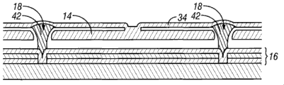
Fig. 1 is the isometric view of a part of describing an embodiment of interferometric modulator display, and wherein the movable reflection horizon of first interferometric modulator is in slack position, and the movable reflection horizon of second interferometric modulator is in actuated position.
Fig. 2 is the system chart that an embodiment of the electronic installation that 3 * 3 interferometric modulator displays are arranged is incorporated in explanation into.
Fig. 3 is the figure at the movable minute surface voltage that position versus applies of an one exemplary embodiment of the interferometric modulator of Fig. 1.
Fig. 4 is can be in order to the explanation of the set of the capable voltage that drives interferometric modulator display and column voltage.
Fig. 5 A and Fig. 5 B explanation can be in order to the capable signal of 3 * 3 interferometric modulator displays that frame of display data are written to Fig. 2 and an exemplary sequential chart of column signal.
Fig. 6 A and Fig. 6 B are the system charts that the embodiment of the visual display unit that comprises a plurality of interferometric modulators is described.
Fig. 7 A is the cross-sectional view of the device of Fig. 1.
Fig. 7 B is the cross-sectional view of an alternate embodiment of interferometric modulator.
Fig. 7 C is the cross-sectional view of another alternate embodiment of interferometric modulator.
Fig. 7 D is the cross-sectional view of the another alternate embodiment of interferometric modulator.
Fig. 7 E is the cross-sectional view of an extra alternate embodiment of interferometric modulator.
Fig. 8 is the plan view from above of an embodiment of interferometric modulator display device.
Fig. 9 is the decomposition diagram of an embodiment of interferometric modulator display device.
Figure 10 is the fragmentary, perspective view of an embodiment of the shaping front substrate of interferometric modulator display device.
Figure 11 A is the cross-sectional view of the shaping front substrate of Figure 10 of piling up of no optics.
Figure 11 B is the cross-sectional view of the shaping front substrate of Figure 11 A after the deposition Optical stack.
Figure 12 A forms the embodiment to the method for the shaping front substrate of the shaping front substrate of Figure 11 B as Figure 10 to Figure 12 D explanation.
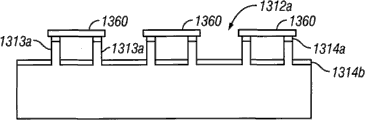
Figure 13 illustrates the array of the interferometric modulator display device of making according to the part of an embodiment or the fragmentary, perspective view of viewing area.
Figure 14 A is the plan view from above of the interferometric modulator display device made of the part of Figure 13.
Figure 14 B is the cross-sectional view of the interferometric modulator display device made of the part of Figure 13 of 14B-14B along the line intercepting.
Figure 14 C is the cross-sectional view of the interferometric modulator display device made of the part of Figure 13 of 14C-14C along the line intercepting, has wherein for the sake of clarity omitted the rear wall that is formed by continuous track.
Figure 14 D is the amplification cross-sectional view of the interferometric modulator display device made of the part of Figure 14 B.
Figure 15 is the plan view from above of the interferometric modulator display device made according to the part of an embodiment, and it schematically illustrates the interconnection that is used for line driver and row driver.
Figure 16 A has a row routing infrastructure and walking along the street plan view from above by the shaping front substrate of structure according to an embodiment.
Figure 16 B is the amplification plan view from above of the walking along the street of Figure 16 A by one in the structure.
Figure 16 C is according to the walking along the street of Figure 16 B of the 16C-16C along the line intercepting of the embodiment cross-sectional view by structure.
Figure 16 D is according to the walking along the street of Figure 16 B of the 16C-16C along the line intercepting of another embodiment cross-sectional view by structure.
Figure 16 E is according to the walking along the street of Figure 16 B that is inserted with anisotropic conductive film therebetween of the embodiment cross-sectional view by structure and line driver.
Figure 16 F is that the walking along the street of Figure 16 E of 16F-16F along the line intercepting is by the cross-sectional view of structure.
Figure 17 A is the fragmentary, perspective view of an embodiment that is used for the routing infrastructure of movable electrode.
Figure 17 B is the cross-sectional view of routing infrastructure of Figure 17 A of 17B-17B along the line intercepting.
Figure 17 C is the cross-sectional view of routing infrastructure of Figure 17 A of 17C-17C along the line intercepting.
Figure 18 A is the fragmentary, perspective view of another embodiment that is used for the routing infrastructure of movable electrode.
Figure 18 B is the cross-sectional view of routing infrastructure of Figure 18 A of 18B-18B along the line intercepting.
Figure 18 C is the cross-sectional view of routing infrastructure of Figure 18 A of 18C-18C along the line intercepting.
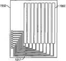
Figure 19 is the plan view from above of an embodiment with carrier of the route trace that engages with the front substrate with stationary electrode for movable electrode.
Figure 20 is the perspective schematic view that an embodiment of the method for using shady shade to form Optical stack on the shaping front substrate is described.
Figure 21 is the perspective schematic view of explanation according to the method for the routing infrastructure of the shady shade formation of the use of embodiment Figure 17 A.
Figure 22 A uses conventional deposition and patterning techniques to make an embodiment of the method for front substrate to Figure 22 C explanation.
Figure 23 A makes an embodiment with method of the front substrate through depositing the preformed support member of patterning before deposited lower electrode and dielectric layer to Figure 23 C explanation.
Figure 24 A and Figure 24 B are the cross-sectional views of the routing infrastructure that engages with the front substrate with stationary electrode of the movable electrode on the carrier according to an embodiment.
Figure 25 is the skeleton view that is used for the shaping carrier that engages with the front substrate with stationary electrode according to an embodiment.
Figure 26 A is the schematic cross section that an embodiment of the method be used for the shaping carrier that engages with the front substrate with stationary electrode is made in explanation to Figure 26 E.
Figure 27 A is the fragmentary, perspective view according to the shaping carrier backboard with rim track and pillar of an embodiment.
Figure 27 B is the cross-sectional view of shaping carrier backboard of Figure 27 A of 27B-27B along the line intercepting.
Figure 27 C is the cross-sectional view of shaping carrier backboard of Figure 27 A of 27C-27C along the line intercepting.
Figure 27 D is the plan view from above of the shaping carrier backboard of Figure 27 A.
Figure 28 is the fragmentary, perspective view according to the shaping carrier backboard of the movable electrode with band etch-hole of another embodiment.
Figure 29 A is a series of schematic cross section that an embodiment of the method for making shaping carrier backboard is described to Figure 29 D.
Figure 30 A makes another embodiment of the method for shaping carrier backboard to Figure 30 D explanation.
Figure 31 A makes the another embodiment of the method for shaping carrier backboard to Figure 31 D explanation.
Figure 32 A is the schematic cross section of the embodiment of shaping carrier backboard to Figure 32 C.
Figure 32 D is the schematic top plan view of the shaping carrier backboard of Figure 32 B.
Figure 32 E is the schematic cross section of marginal portion of the shaping carrier backboard of Figure 32 D.
Figure 33 A makes the another embodiment of the method for the shaping carrier backboard with patterned movable electrode to Figure 33 D explanation.
Figure 34 A is the schematic partial perspective view of the interferometric modulator display device of the excessive mechanical layer support member that raises between the movable electrode band according to having of an embodiment.
Figure 34 B is respectively the schematic cross section of interferometric modulator display device of Figure 34 A of 34B-34B along the line, 34C-34C and 34D-34D intercepting to Figure 34 D.
Figure 35 A and Figure 35 B are that the perspective schematic view of an embodiment of method be used for movable electrode is transferred to the removable carrier of front substrate is made in explanation.
Figure 35 C and Figure 35 D are the schematic cross section that an embodiment of the method for using removable carrier to make the interferometric modulator display device is described.
Figure 36 A is the schematic cross section that an embodiment of the method for making the carrier with patterned movable electrode is described to Figure 36 E.
Figure 37 A makes another embodiment of the method for the carrier with patterned movable electrode to Figure 37 E explanation.
Figure 38 A makes the another embodiment of the method for the carrier with patterned movable electrode to Figure 38 D explanation.
Figure 39 A is the schematic cross section that is used for the carrier that engages with front substrate according to an embodiment, and described carrier has the riveting parts supporting construction.
Figure 39 B is the schematic cross section according to the interferometric modulator display device of the riveting parts supporting construction with Figure 39 A that reverses on the substrate support structure forwardly of an embodiment.
Figure 40 is the perspective schematic view of an embodiment of interferometric modulator display device.
Figure 41 A schematically illustrates according to the route of the interferometric modulator display device of various embodiment to Figure 41 C and arranges.
Figure 42 A explanation is arranged according to the route of the interferometric modulator display device of another embodiment.
Figure 42 B and Figure 42 C are respectively the cross-sectional views of interferometric modulator display device of Figure 42 A of 42A-42A along the line and 42B-42B intercepting.
Figure 43 A is that explanation uses the carrier of the backboard also serve as finishing device to make the perspective schematic view of an embodiment of the method for interferometric modulator display device, and Figure 43 B is the schematic cross section that described embodiment is described to Figure 43 C.
Figure 44 A is that explanation cooperates conductive seal agent on the front substrate to use the schematic plan view of an embodiment of the method for shady shade, Figure 44 B is the zoomed-in view of the described embodiment of explanation, and Figure 44 C is the schematic cross section of the described embodiment of explanation to Figure 44 E.
Figure 45 A is the schematic cross section that an embodiment of the method for using removable carrier to make the interferometric modulator display device is described to Figure 45 D.
Figure 46 A is the cross-sectional view of an embodiment with interferometric modulator display device of the sept that extends between movable electrode layer and backboard.
Figure 46 B is the skeleton view of interferometric modulator display device with Figure 46 A of the sept that captures the movable electrode layer and support member.
Figure 47 is the skeleton view of another embodiment with interferometric modulator display device of the sept that extends through the movable electrode layer.
Figure 48 is the skeleton view of another embodiment with interferometric modulator display device of sept.
Figure 49 A is the cross-sectional view of an embodiment with interferometric modulator display device of the stop pillar that extends from backboard.
Figure 49 B is the cross-sectional view of another embodiment with interferometric modulator display device of the stop pillar that extends from backboard.
Figure 49 C is the cross-sectional view of another embodiment with interferometric modulator display device of the stop pillar that extends from backboard.
Figure 50 is the cross-sectional view of an embodiment that does not have the interferometric modulator display device of support member in its viewing area.
Figure 51 has the cross-sectional view of an embodiment of interferometric modulator display device that extends to the sept of front substrate from backboard.
Figure 52 A is the cross-sectional view of an embodiment with interferometric modulator display device of patterned black mask.
Figure 52 B is the plan view from above according to the interferometric modulator display device of Figure 50 A of an embodiment.
Figure 53 A makes an embodiment of the method for the local moistening black mask that is used for the interferometric modulator display device to Figure 53 C explanation.
Another embodiment that Figure 53 D explanation has the interferometric modulator display device of local moistening black mask.
Figure 54 is the cross-sectional view of an embodiment that comprises the static interferometric display of shaping front substrate.
Figure 55 is the cross-sectional view of another embodiment that comprises the static interferometric display of shaping backboard.
Figure 56 is the plan view from above of the static interferometric display of Figure 54.
Figure 57 is the cross-sectional view of another embodiment that comprises the static interferometric display of shaping front substrate.
Figure 58 comprises the shaping front substrate and the cross-sectional view of the another embodiment of the static interferometric display of useless independent support member in each pixel.
Figure 59 is the plan view from above of the static interferometric display of Figure 58.
Figure 60 is the cross-sectional view of another embodiment that comprises the static interferometric display of shaping backboard.
Figure 61 is the cross-sectional view of another embodiment that comprises the static interferometric display of shaping front substrate.
Embodiment
Below describing in detail is at some specific embodiment of the present invention.Yet the present invention can implement by many different modes.Referring to graphic, wherein identical parts is represented with same numeral all the time in this describes.As will understanding easily from following description, described embodiment can implement in any device that is configured to display image (no matter being still still image (for example, rest image) of moving image (for example, video), and no matter be character image or graph image).More particularly, expect that described embodiment can implement or associated in multiple electronic installation, described electronic installation for example (but being not limited to) is a mobile phone, wireless device, personal digital assistant (PDA), hand-held or portable computer, gps receiver/navigating instrument, camera, the MP3 player, hand-held camera, game console, watch, clock and watch, counter, TV monitor, flat-panel monitor, computer monitor, automatic display (for example, mileometer display etc.), driving cabin controller and/or display, camera visual field display (for example, the display of the rear view camera in the vehicle), electronic photo, electronics bulletin board or electronic marker, projector, building structure, encapsulation and aesthetic structures (for example, the demonstration of the image on jewelry).The MEMS device that has similar structures with MEMS device as herein described also can be used for for example being used for electronic switching device in the non-display application.
Can make MEMS (micro electro mechanical system) (MEMS) device by attached two substrates, each in the described substrate has preformed assembly thereon.Comprising according to the method for the manufacturing MEMS device of an embodiment provides front substrate and is formed at stationary electrode on the front substrate.Then, the carrier that will comprise movable electrode formed thereon is attached to front substrate.The carrier of some embodiment can be released after movable electrode is transferred to front substrate; In other embodiments, carrier serves as the backboard of MEMS.Can be by deposition and patterning, form feature by impression or by patterning and etching.Described method not only reduces manufacturing cost, but also less variation is provided, and therefore provides higher yield.Gained MEMS device is difficult for being stressed and changes and the moisture leakage contribution.Also disclose from movable electrode and be routed to row driver and be routed to the method for line driver from stationary electrode.Also teaching is used to form black mask to prevent the technology of unwanted reflection in the optical MEMS (for example, interferometric modulator).
Explanation comprises an interferometric modulator display embodiment of interfere type MEMS display element among Fig. 1.In these devices, pixel is in bright state or dark state.Under bright (" connection " or " opening ") state, display element reflects the major part of incident visible light to the user.When being in dark (" disconnection " or " closing ") state, display element reflects the incident visible light to the user hardly.Decide on embodiment, can put upside down the reflective character of " connection " and " disconnection " state.The MEMS pixel can be configured to mainly reflect under selected color, thereby allows the colour except that black and white to show.
Fig. 1 is an isometric view of describing two neighborhood pixels in a series of pixels of visual displays, and wherein each pixel comprises a MEMS interferometric modulator.In certain embodiments, interferometric modulator display comprises the row/column array of these interferometric modulators.Each interferometric modulator comprises a pair of reflection horizon, and both locate at a distance of variable and controllable distance each other, have at least one variable-sized optical resonance cavity with formation.In one embodiment, one in the described reflection horizon can be moved between the two positions.In primary importance (this paper is called slack position), movable reflection horizon is positioned at apart from the fixing relatively large distance of partially reflecting layer.In the second place (this paper is called actuated position), movable reflection horizon is positioned at and closer is adjacent to described partially reflecting layer place.Look the position in movable reflection horizon and long mutually or interfere mutually from the incident light of two layers reflection with disappearing, thereby produce comprehensive the reflection or non-reflective state for each pixel.
Institute's drawing section branch of the pel array among Fig. 1 comprises two adjacent interferometric modulators 12a and 12b.Among the interferometric modulator 12a of on the left side, movable reflection horizon 14a is illustrated as and is in the slack position at a distance of preset distance with Optical stack 16a, and Optical stack 16a comprises partially reflecting layer.Among the interferometric modulator 12b on the right, movable reflection horizon 14b is illustrated as and is in the actuated position that is adjacent to Optical stack 16b.
Optical stack 16a as referred herein and 16b (being referred to as Optical stack 16) generally include several fused layers (fused layer), described fused layers can comprise the electrode layer of tin indium oxide (ITO) for example, the partially reflecting layer of for example chromium, and transparent dielectric.Optical stack 16 is therefore for conduction, partially transparent and partial reflection, and can (for example) by making with one or more the depositing on the transparent substrates 20 in the upper strata.In certain embodiments, described layer pattern is turned to parallel band, and can be as hereinafter further describing the column electrode that forms in the display device.Movable reflection horizon 14a, 14b can be formed depositing metal layers (vertical) on the top that is deposited on pillar 18 and the series of parallel band that is deposited on the intervention expendable material between the pillar 18 with the column electrode of 16a, 16b.When expendable material was etched, gap or cavity 19 that movable reflection horizon 14a, 14b pass through to be defined were opened with Optical stack 16a, 16b branch.For example the material of the highly conductive of aluminium and reflection can be used for reflection horizon 14, and these bands can form the row electrode in the display device.
Illustrated as the pixel 12a among Fig. 1, do not applying under the voltage condition, cavity 19 remains between movable reflection horizon 14a and the Optical stack 16a, and wherein movable reflection horizon 14a is in the mechanical relaxation state.Yet when potential difference (PD) being applied to selected row and column, the capacitor that is formed at the intersection of the column electrode at respective pixel place and row electrode becomes charged, and electrostatic force is pulled in electrode together.If voltage is enough high, 14 distortion of so movable reflection horizon, and be forced on the Optical stack 16.Pixel 12b as the right among Fig. 1 is illustrated, and the dielectric layer (undeclared among this figure) in the Optical stack 16 can prevent the distance of separation between short circuit and key-course 14 and the layer 16.Regardless of the polarity of the potential difference (PD) that is applied, behavior all is identical.In this way, may command reflective pixel state contrasts the row of non-reflective pixel state/row and activates and be similar to employed row in conventional LCD and other display technique/row actuating in many aspects.
Fig. 2 is used for using in display application the example procedure and the system of interferometric modulator array to Fig. 5 explanation.
Fig. 2 is the system chart that explanation can be incorporated an embodiment of the electronic installation that aspect of the present invention is arranged into.In an exemplary embodiment, electronic installation comprises processor 21, processor 21 for example can be ARM,
 Pentium
 Pentium
Pentium
Pentium
 Pro, 8051,
 Power
Any general purpose single-chip or multicore sheet microprocessor, or any special microprocessor of digital signal processor, microcontroller or programmable gate array for example.As in this key technology for the routine be that
Power
Any general purpose single-chip or multicore sheet microprocessor, or any special microprocessor of digital signal processor, microcontroller or programmable gate array for example.As in this key technology for the routine be that processor 21 can be configured to carry out one or more software modules.Except that executive operating system, processor can be configured to carry out one or more software applications, comprises web browser, telephony application, e-mail program, or any other software application.
In one embodiment, processor 21 also is configured to communicate by letter with array driver 22.In one embodiment, array driver 22 comprises row driver circuits 24 and the column driver circuit 26 that signal is provided to panel or display array (display) 30.The xsect of showing array illustrated in fig. 1 among Fig. 2 with line 1-1.For the MEMS interferometric modulator, OK/the row actuation protocol can utilize the hysteresis characteristic of these devices illustrated in fig. 3.May need the potential difference (PD) of (for example) 10 volts to cause movable layer to be deformed into actuating state from relaxed state.Yet, when voltage when described value reduces, movable layer is got back to and is lower than 10 volts and keep its state along with voltage drop.In the one exemplary embodiment of Fig. 3, drop at voltage and to be lower than before 2 volts, movable layer can be not lax fully.Therefore, there be the voltage range of about 3V in the illustrated example of Fig. 3, wherein have the voltage window that applies, install described applying and be stable at relaxed state or actuating state in the voltage window to 7V.This window is known as " lag window " or " stability window " in this article.For the display array of hysteresis characteristic with Fig. 3, can design row/row actuation protocol, during the feasible gating of being expert at, pixel to be activated is exposed to about 10 volts voltage difference in selected the passing through, and pixel to be relaxed is exposed to the voltage difference that approaches zero volt.After gating, it is poor that described pixel is exposed to about 5 volts steady state voltage, makes described pixel still be in any state that capable gating puts it into.After being written into, each pixel experience is " stability window " interior potential difference (PD) of 3 volts to 7 volts in this example.This feature makes pixel design illustrated in fig. 1 be stable under identical institute's voltage conditions that applies and activates or the lax state that is pre-stored in.Owing to no matter be in actuating state or relaxed state, each pixel of interferometric modulator is equal capacitors for being formed by fixed reflector and mobile reflection horizon in essence, so can keep this steady state (SS) under the voltage in lag window under the situation that inactivity almost dissipates.If the current potential that is applied is fixed, no current flows in the pixel so in essence.
In the typical case uses, can assert that the row electrode is gathered and produce display frame by gathering according to the institute's actuate pixel of wanting in first row.Then, apply horizontal pulse, thereby activate pixel corresponding to the alignment of being asserted to row 1 electrode.Then, the row electrode of being asserted set is changed into corresponding to the institute's actuate pixel of wanting in second row gathered.Then, apply pulse, thereby activate suitable pixel in the row 2 according to the row electrode of being asserted to row 2 electrodes.Row 1 pixel is not influenced by row 2 pulses, and still is in the state that its 1 impulse duration of being expert at is set to.This process can repeat to produce frame in mode in proper order at whole row series.Usually, by being wanted a number frame to repeat this process continuously to refresh and/or upgrade described frame with new video data so that per second is a certain.The column electrode and the row electrode that are used to drive pel array also are well-known with the various protocols that produces display frame, and it can use in conjunction with the present invention.
Fig. 4 and Fig. 5 illustrate a kind of in order to produce the possible actuation protocol of display frame on 3 * 3 arrays of Fig. 2.Fig. 4 explanation can be used for showing the possible row and the set of row voltage level of pixel of the hysteresis curve of Fig. 3.In the embodiment of Fig. 4, actuate pixel relates to suitable row is set at-V
Bias, and suitable row is set at+Δ V, it can correspond respectively to-5 volts and+5 volts.By suitable row are set at+V
BiasThereby and suitable row is set at identical+Δ V and on pixel, produces zero volt potential difference (PD) and realize making pixel lax.The voltage of being expert at remains in those row of zero volt, does not have to discuss point by point to be in+V
BiasStill-V
Bias, pixel all is stable at its initial residing any state.Also as illustrated in fig. 4, will understand, and can use the opposite polarity voltage of polarity and voltage mentioned above, for example, actuate pixel can relate to suitable row are set at+V
Bias, and suitable row is set at-Δ V.In this embodiment, by suitable row are set at-V
BiasThereby and suitable row is set at identical-Δ V and on pixel, produces zero volt potential difference (PD) and realize making pixel to discharge.
Fig. 5 B shows to be applied to and will to produce the sequential chart of a series of row and column signals of 3 * 3 arrays that the Fig. 2 of (wherein actuate pixel is non-reflexive) is arranged in demonstration illustrated among Fig. 5 A.Before the illustrated frame, described pixel can be in any state in writing Fig. 5 A, and in this example, all row all are in 0 volt, and all row all be in+5 volts.Under these institute's voltages that apply, all pixels all are stable at its existing actuating or relaxed state.
In the frame of Fig. 5 A, actuate pixel (1,1), (1,2), (2,2), (3,2) and (3,3).For realizing this purpose, during be expert at 1 " line time ", row 1 and 2 are set at-5 volts, and row 3 are set at+5 volts.This measure does not change the state of any pixel, because all pixels all remain in 3 volts to 7 volts the stability window.Then use and be raised to 5 volts from 0 volt and turn back to zero pulse again row 1 is carried out gating.This measure activates (1,1) and (1,2) pixel and lax (1,3) pixel.Other pixel in the array is unaffected.For setting row 2 on demand, row 2 are set at-5 volts, and row 1 and 3 are set at+5 volts.The same strobe that is applied to row 2 is then with actuate pixel (2,2) and relax pixels (2,1) and (2,3).Equally, other pixel of array is unaffected.Set row 3 similarly by row 2 and 3 being set at-5 volts and row 1 are set at+5 volts.Row 3 gatings are set row 3 pixels as shown in Fig. 5 A.After writing incoming frame, the row current potential is zero, and the row current potential can remain on+5 volts or-5 volts, and display then is stable in the layout of Fig. 5 A.To understand, same program can be used for the array of tens of or hundreds of row and columns.Also will understand, in the General Principle of above-outlined, can change widely in order to carrying out sequential, sequence and the level of the voltage that row and column activates, and above example is exemplary, and any actuation voltage method all can be used with system and method as herein described.
Fig. 6 A and Fig. 6 B are the system charts of the embodiment of explanation display device 40.Display device 40 can be (for example) honeycomb fashion or mobile phone.Yet the same components of display device 40 or its slight variation also illustrate various types of display device, for example TV and portable electronic device.
The display 30 of exemplary display device 40 can be any one in the multiple display (comprising bistable display as described herein).In other embodiments, display 30 comprises flat-panel monitor as indicated above (for example plasma, EL, OLED, STN LCD or TFT LCD), or non-tablet display (for example CRT or as well-known other tubular device of those skilled in the art).Yet for the purpose of describing present embodiment, display 30 comprises interferometric modulator display as described herein.
The assembly of an embodiment of exemplary display device 40 schematically is described among Fig. 6 B.Illustrated exemplary display device 40 comprises shell 41, and can comprise the partially enclosed at least additional assemblies in described shell 41.For instance, in one embodiment, exemplary display device 40 comprises network interface 27, and it comprises antenna 43, and antenna 43 is coupled to transceiver 47.Transceiver 47 is connected to processor 21, and processor 21 is connected to regulates hardware 52.Regulate hardware 52 and can be configured to conditioning signal (for example, signal being carried out filtering).Regulate hardware 52 and be connected to loudspeaker 45 and microphone 46.Processor 21 is also connected to input media 48 and driver controller 29.Driver controller 29 is coupled to frame buffer 28, and is coupled to array driver 22, and array driver 22 is coupled to display array 30 again.Power supply 50 provides electric power to all component as the design of particular exemplary display device 40.
In alternate embodiment, transceiver 47 can be replaced by receiver.In another alternate embodiment, network interface 27 can be replaced by image source, and the view data that is sent to processor 21 can be stored or be produced to described image source.For instance, image source can be digital video disc (DVD) or the hard disk drive that contains view data, or produces the software module of view data.
In one embodiment, processor 21 comprises the operation with control exemplary display device 40 of microcontroller, CPU or logical block.Regulating hardware 52 comprises usually in order to signal is transmitted into loudspeaker 45 and in order to amplifier and wave filter from microphone 46 received signals.Adjusting hardware 52 can be the discrete component in the exemplary display device 40, maybe can be incorporated in processor 21 or other assembly.
Usually, array driver 22 receives through formative information from driver controller 29, and video data is reformatted as one group of parallel waveform, and described waveform per second many times is applied to the hundreds of and thousands of sometimes lead-in wires from the x-y picture element matrix of display.
In one embodiment, driver controller 29, array driver 22 and display array 30 are applicable to any in the display of type described herein.For instance, in one embodiment, driver controller 29 is conventional display controller or bistable state display controller (for example, interferometric modulator controller).In another embodiment, array driver 22 is conventional driver or bi-stable display driver (for example, interferometric modulator display).In one embodiment, driver controller 29 is integrated with array driver 22.This embodiment is common to for example height integrated system of cellular phone, wrist-watch and other small-area display.In another embodiment, display array 30 is typical display array or bi-stable display array (display that for example, comprises interferometric modulator array).
As indicated above, in some embodiments, the control programmability resides on the driver controller of some positions that can be arranged in electronic display system.In certain embodiments, the control programmability resides in the array driver 22.Those skilled in the art will realize that hardware that optimization mentioned above can any number and/or component software and implement with various configurations.
Details according to the structure of the interferometric modulator of above-mentioned operate can change widely.For instance, Fig. 7 A illustrates five different embodiment of movable reflection horizon 14 and supporting construction thereof to Fig. 7 E.Fig. 7 A is the xsect of the embodiment of Fig. 1, and wherein strip of metal material 14 is deposited on the vertically extending support member 18.In Fig. 7 B, movable reflection horizon 14 only relies on drift bolt 32 to be attached to support member around the corner.In Fig. 7 C, movable reflection horizon 14 is suspended from deformable layer 34, and deformable layer 34 can comprise the flexible metal.Deformable layer 34 is connected to substrate 20 directly or indirectly in each position.Described connection is called supporting construction or pillar 18 herein.Illustrated embodiment has the supporting construction 18 that comprises support post plug 42 among Fig. 7 D, and deformable layer 34 is held on the support post plug 42.Movable reflection horizon 14 still as Fig. 7 A is in Fig. 7 C is suspended on the cavity, but deformable layer 34 does not form support column 18 by the hole between filling deformable layer 34 and the Optical stack 16.Truth is that support column 18 is by forming in order to the planarisation material that forms support post plug 42.Illustrated embodiment is based on the embodiment shown in Fig. 7 D among Fig. 7 E, but also can be suitable for cooperating Fig. 7 A any one among the illustrated embodiment and not shown extra embodiment and work in Fig. 7 C.In the embodiment shown in Fig. 7 E, used the additional layer of metal or other conductive material to form bus structure 44.This allows the signal route along the interferometric modulator rear portion, thereby eliminates otherwise possible many electrodes that must form on substrate 20.
In the embodiment of embodiment for example shown in Figure 7, interferometric modulator serves as Direct-View Device, in described Direct-View Device, watches image from the front side (with the top relative side of side that is furnished with movable electrode) of transparent substrates 20.In these embodiments, reflection horizon 14 comprises deformable layer 34 and bus structure 44 with the some parts of optical mode shielding interferometric modulator on the side relative with substrate 20 in reflection horizon.This allows not influencing negatively under the situation of picture quality the district that is shielded to be configured and to operate on it.It is selected that this discerptible modulator architecture allows to be used for the structural design and the material of the dynamo-electric aspect of modulator and optics aspect, and work independently of one another.In addition, Fig. 7 C has from the optical characteristics of carrying out by deformable layer 34 that makes reflection horizon 14 to the embodiment shown in Fig. 7 E and separates the additional benefit that obtains with its mechanical property.This permission is optimized structural design and the material that is used for reflection horizon 14 with respect to optical characteristics, and optimizes structural design and the material that is used for deformable layer 34 with respect to desired mechanical property.
Catalogue
I. make interferometric modulator by attached substrate ... ... ... ... ... ... ... ... ... 20
II. the formation of front substrate ... ... ... ... ... ... ... ... ... ... .... 21
1. the formation of shaping front substrate ... ... ... ... ... ... ... ... ... ... .... 22
2. the formation of patterned front substrate ... ... ... ... ... ... ... ... ... ... 31
3. the formation of preformed support member front substrate ... ... ... ... ... ... ... ... ... .. 32
4. other row routing infrastructure ... ... ... ... ... ... ... ... ... ... ... .. 33
III. the formation of rear portion carrier ... ... ... ... ... ... ... ... ... ... ... 34
1. shaping carrier ... ... ... ... ... ... ... ... ... ... ... ... .. 34
A. the carrier backboard is shaped ... ... ... ... ... ... ... ... ... ... ... .... 35
B. removable carrier is shaped ... ... ... ... ... ... ... ... ... ... ... .. 42
2. the carrier that has patterned movable electrode ... ... ... ... ... ... ... ... ... .. 43
A. the carrier backboard that has patterned movable electrode ... ... ... ... ... ... ... ... .... 43
B. the removable carrier that has patterned movable electrode ... ... ... ... ... ... ... ... .. 45
IV. lamination ... ... ... ... ... ... ... ... ... ... ... ... .. 46
1. shaping carrier backboard and shaping front substrate ... ... ... ... ... ... ... ... ... .. 46
A. embodiment A ... ... ... ... ... ... ... ... ... ... ... ... ... 46
D. route option 4....................................................... ... ... ... 49
E. encapsulate and seal ... ... ... ... ... ... ... ... ... ... ... ... 49
B. Embodiment B ... ... ... ... ... ... ... ... ... ... ... ... ... 51
2. shaping carrier backboard and patterned front substrate ... ... ... ... ... ... ... ... .... 51
3. shaping carrier backboard and preformed support member front substrate ... ... ... ... ... ... ... ... 52
4. removable carrier and shaping front substrate are shaped ... ... ... ... ... ... ... .. 52
5. removable carrier and patterned front substrate are shaped ... ... ... ... ... ... .... 53
6. removable carrier and preformed support member front substrate are shaped ... ... ... ... ... ... 53
7. the carrier backboard and the shaping front substrate that have patterned movable electrode ... ... ... .. 53
8. the carrier backboard and the patterned front substrate that have patterned movable electrode ... ... .. 54
9. the carrier backboard and the preformed support member front substrate that have patterned movable electrode ... .. 54
10. the removable carrier and the shaping front substrate that have patterned movable electrode ... .... 55
11. have the removable carrier and the patterned front substrate of patterned movable electrode ... .... 55
12. have the removable carrier and the preformed support member front substrate of patterned movable electrode .... 55
13. the conventional deposition of shaping front substrate and movable electrode ... ... ... ... ... .... 56
V. be used to keep the sept at the interval between front substrate and the backboard ... ... ... ... ... .. 56
VI. black mask ... ... ... ... ... ... ... ... ... ... ... 59
1. patterned black mask ... ... ... ... ... ... ... ... ... .. 59
2. local moistening black mask ... ... ... ... ... ... ... ... ... .. 60
VII. static interferometric display ... ... ... ... ... ... ... ... ... 60
1. the static interferometric display that has shaping or preformed support member front substrate ... ... ... ... 61
2. the static interferometric display that has shaping or preformed backboard ... ... ... ... ... .... 63
3. the static interferometric display that has the cavity filling agent ... ... ... ... ... ... .... 64
4. the static interferometric display that has continuous degree of depth cavity ... ... ... ... ... ... .. 66
I. make interferometric modulator by attached substrate
In certain embodiments, can make the MEMS device by attached two substrates, each in the described substrate has preformed assembly thereon.In addition, described two substrates can be made by the different manufacturers with the equipment that is fit to each substrate of manufacturing respectively.Then, described substrate can be fitted together by the 3rd fabricator.Assembling process also can help to reduce movable layer deviation and therefore reduce to cross over array from the MEMS assembly to the MEMS assembly or the cavity size variability from the array to the array.This makes dirigibility and not only reduces whole cost, but also higher yield is provided.In addition, some embodiment among the hereinafter described embodiment promote unsheltered patterning (for example, photoetching), and therefore can be by avoiding reducing manufacturing cost in order to the complex steps of setting up configuration with a plurality of thin layers.
MEMS device by process manufacturing described herein can have relative less clearance (for example, about 6,500 between two substrate
And between about 20 μ m, and particularly between about 2 μ m and about 15 μ m or about 10,000
And between about 5 μ m).Among the described in the present invention embodiment, when the gap between two substrates (that is, front substrate and backboard) refers generally to overlie on the front substrate for the bottom surface of the deep trouth of front substrate and backboard towards the gap between the back plate surface of front substrate.Described back plate surface is apart from front substrate surface farthest.To understand better from description hereinafter " two substrate between gap " about the lamination of shaping carrier backboard and shaping front substrate.In addition, the MEMS device can have and spreads all over its array region but not only at the support member or the sept of its edge.Therefore, the MEMS device is difficult for the variable effect that is stressed.In addition, relatively less clearance needs the less sealant between two substrates, even and therefore under the situation of the inner no drying agent of MEMS device, the MEMS device more is not subject to the moisture leakage contribution yet.In addition, the MEMS device may have elongated profile owing to the less clearance size.
Among the embodiment hereinafter,, in the environment of interferometric modulator the MEMS device is described in particular at the optical MEMS device.Yet, be understood by those skilled in the art that process described herein is applicable to other MEMS device, for example the dynamo-electric capacitance-type switch of the optical MEMS of other type or MEMS.
Fig. 8 explanation is according to the interferometric modulator display device 800 of an embodiment.Interferometric modulator display device 800 comprises viewing area 801 and outer peripheral areas 802.
Outer peripheral areas 802 is around viewing area 801.Viewing area 801 is also referred to as " array region " in this article, because it comprises the electrostatic MEMS cellular array of indivedual actuatings.Outer peripheral areas 802 can comprise driver chip zone and interconnection or routing infrastructure.Device 800 can have line driver 811 and the row driver 812 that is installed on the driver chip zone.Driver 811 and 812 can be installed on the driver chip zone by using any suitable joining technique, and described joining technique engages, is with and carries encapsulation (TCP) film attached or on glass (FOG) joint including (but not limited to) glass top chip (COG).Routing infrastructure is configured to respectively column electrode and row electrode are electrically connected to line driver 811 and row driver 812.
Can form the interferometric modulator display device 800 of Fig. 8 by front substrate being attached to backboard.Fig. 9 explanation is according to the method for the manufacturing interferometric modulator display device 900 of an embodiment.At first, provide front substrate 910 with demonstration or array region 901 and outer peripheral areas 902.Front substrate 910 can comprise the cavity that is arranged in viewing area 901 or the array of groove.But each self-contained Optical stack that comprises fixing or stationary electrode of cavity or groove.As describing with respect to Fig. 8, front substrate 910 also can comprise routing infrastructure and the driver chip zone that is arranged in outer peripheral areas 902.
Then, the carrier 950 that will be used to carry some functional modules of interferometric modulator display device 900 is attached to front substrate 910, thereby covers viewing area 901 and around the part of the outer peripheral areas 902 of viewing area 901.In one embodiment, before carrier 950 is attached to front substrate 910, on carrier 950, form movable electrode.When anterior substrate 910 is attached to each other with carrier 950, movable electrode is inserted therebetween.Can movable electrode be attached to the supporting construction of front substrate 910 by using (for example) anodic bonding, fusion joint and similar approach.
In certain embodiments, on the carrier that can be removable carrier (for example, seeing that Figure 35 A is to Figure 35 D and additional the description), form movable electrode.In other embodiments, carrier serve as display device 900 permanent backboard (for example, see Figure 25 to Figure 34 D and Figure 36 A to Figure 39 B and additional the description).In another embodiment, before permanent backboard is attached to front substrate, forwardly form movable electrode on the substrate.Then, backboard is attached to front substrate.
II. the formation of front substrate
In making interferometric modulator display device as described above, may be formed in various ways the front substrate of device.In one embodiment, can and then in cavity, form Optical stack, prepare front substrate by the cavity in the surface that form to arrive substrate or dimple.Can form cavity by any suitable procedure (for example, impression, photoetching and etching and stamp).In the context of this document, the front substrate that process is thus formed is called " shaping front substrate ".Usually, cavity is by delimiting with the integrally formed support member of substrate (for example, track or pillar) of the front substrate that is used to be shaped.
In another embodiment, can be by preparing front substrate to define cavity forming Optical stack on the substrate and then on Optical stack, form support member.In the context of this document, the front substrate that process is thus formed is called " patterned front substrate ".Usually, support member separates with substrate and is formed at the substrate top, and can be made (for example, seeing that Figure 22 A is to Figure 22 C and additional the description) by the material different with the substrate that is used for patterned substrate.
In another embodiment, can be by making front substrate to define cavity and then in cavity, to form Optical stack at formation pillar on the substrate.In the context of this document, the front substrate that process is thus formed is called " preformed support member front substrate ".As patterned front substrate, preformed support member front substrate has the pillar that separates with substrate and can be made by the material that is different from substrate; Be different from patterned front substrate, Optical stack (comprising stationary electrode) do not inserted between support member and the substrate.
1. the formation of shaping front substrate
Figure 10 is the schematic partial perspective view according to the shaping front substrate 1000 of an embodiment.The illustrated part of front substrate 1000 is parts of the viewing area of front substrate 1000.Therefore, it should be noted that Figure 10 is the local specification of viewing area, and therefore, structure shown in Figure 10 repeats on whole viewing area substantially.
As shown in figure 10, track 1011a extends to parallel to each other the going up at line direction (x direction) of 1011d.To understand, OK/row or the expression of XYZ direction be essentially arbitrarily, but in this article with reference consistently.Track 1011a makes its top surface be in identical substantially height to 1011d, that is, and and in single plane.
As shown in figure 10, groove 1012a replaces to 1011d to 1012c and track 1011a, and parallel to each other going up at line direction (x direction) extended.As understanding better from the following description content, groove 1012a is that movable electrode (not shown) provides cavity or space to subside towards anterior substrate 1010 to 1012c.
For illustrated interferometric modulator embodiment, groove 1012a can have between about 600 to 1012c
 With about 4,000
 Between the degree of
 depth.Groove 1012a has various depth D 1, D2, D3 to the visual groove 1012a of 1012c to 1012c through designing the color that produces with the operating period in the gained display device.In the illustrated embodiment, front substrate 1000 has first, second and the three-flute that has three different depth D1, D2, D3 at three different colors.The first groove 1012a has minimum-depth and is configured to produce blue (B) color.The first groove 1012a can have between about 600
 With about 2,000
 Between first depth D 1.The
 second groove 1012b has moderate depth and is configured to produce green (G) color.The second groove 1012b can have between about 1,000
 With about 3,000
 Between second depth D 2.Three-
flute 1012c has depth capacity and is configured to produce red (R) color.Three-flute 1012c can have between about 2,000
 With about 4,000
 Between the 3rd depth D 3.
Groove 1012a can have width W between about 10 μ m and about 200 μ m to 1012c.Be understood by those skilled in the art that groove 1012a is to the color of the configuration of 1012c and depth visual pixel and design and change.


The conductive layer of the Optical stack 1014 of groove 1012a to the bottom surface of 1012c is electrically isolated from one to 1011d by track 1011a.The conductive layer that electricity is isolated forms the column electrode of gained interferometric modulator display device.
In certain embodiments, Optical stack 1014 also can comprise the metal absorber layers (or partially reflecting layer) between transparency conducting layer and dielectric layer.Described absorber layers can be formed by the metal of for example chromium (Cr), molybdenum (Mo) or the Mo/Cr of translucent thickness.In another embodiment of broadband white light interference formula modulator, the semiconductor layer of available for example germanium layer replaces absorber layers.Absorber layers or semiconductor layer can have between about 1
 With about 100
 Between, in particular between about 50
 With about 100
Between thickness.
With about 100
Between thickness.
Figure 11 A is the cross-sectional view of front substrate 1000 (no optics piles up 1014) of Figure 10 of 11A-11A along the line intercepting.Because the difference of the degree of depth, groove 1012a is in differing heights L1a, L1b, L1c respectively to the basal surface of 1012c.Yet, because support member 1011a has the differing heights to the degree of depth of 1012c corresponding to groove 1012a to 1011d and 1013a to 1013c, so the top surface of support member 1011a to 1011d and 1013a to 1013c is in sustained height L2 substantially, that is, substantially in same plane.
Optical stack on the top of support member 1011a to 1011d, 1013a to 1013c can be served as " black mask ".Optical stack provides identical optical effect all the time when interferometric modulator is in it and subsides state.Optical stack can provide black color.In other embodiments, Optical stack is looked the interferometric modulator design and color white can be provided.
Figure 11 B is the cross-sectional view of Figure 11 A after deposition Optical stack 1014.Because Optical stack 1014, the peak of front substrate 1000 is in the height L2 ' that exceeds the thickness of Optical stack 1014 than height L2 and locates.
Figure 12 A is the cross-sectional view of explanation according to the method for the formation shaping front substrate of an embodiment to Figure 12 D.Illustrated method uses impression that front substrate is shaped.Shown in Figure 12 A, the substrate 1210 of general planar is placed on the pressing plate 1220.Substrate 1210 other material (being preferably transparent) that is ductile to be used to be shaped that can or be easy to become by glass forms.Illustrated pressing plate 1220 can be formed by metal material.But heated substrate 1210 makes substrate 1210 enough soft to impress when the follow-up imprint step.Substrate 1210 can be heated to and look the material that is used for substrate 1210 and the temperature that changes.
Then, shown in Figure 12 B, platen 1230 is pressed on softening substrate 1210.Platen 1230 has through being shaped to define the dimple and the projection of track, groove and pillar on the substrate 1210.Platen 1230 can be formed by metal material.In certain embodiments, the form of at least one rotating cylindrical body taked in pressing plate 1220 and the platen 1230.Be understood by those skilled in the art that various other configurations of stamping technique also can be suitable for making front substrate 1210 to be shaped.
Then, remove platen 1230 from front substrate 1210.Subsequently, from pressing plate 1220 remove through the impression front substrate 1210.The front substrate 1210 of showing gained among Figure 12 C.
In another embodiment, front substrate 1210 is shaped.In another embodiment, predetermined portions that can be by the substrate of at first stamping and then optionally the described part of etching front substrate 1210 is shaped.Term " stamp " can use convertibly with mark or line.Can use the various technology of machining for example or laser stamp to stamp.Automatically the stamp method can (Nippon Sheet Glass, Co. Ltd) buys from the NHTechno company of Tokyo.Can under the situation of no masking process, carry out Figure 12 A to the stamping technique shown in Figure 12 D.In addition, patterned plate can be recycled and reused for many substrates.To understand, various other technology also can be used for making front substrate 1210 to be shaped.
Subsequently, cross over shaping front substrate 1210 sequential deposition Optical stack materials substantially.For example can use that any appropriate technology of sputter deposits the Optical stack material, make Optical stack 1214 be deposited on the top of support member and be deposited on the bottom surface of groove, but enough not conformally cover to obtain continuous side walls.This configuration can be applicable to any MEMS device (optics or non-optical MEMS device).Optical stack on the top of support member can be served as optical MEMS device " black mask ".The configuration of Optical stack 1214 can be described about the Optical stack 1014 of Figure 10 as mentioned.
Figure 13 is the fragmentary, perspective view of an embodiment of the interferometric modulator display device 1300 made of part, is furnished with the front substrate 1310 of movable electrode 1360 above interferometric modulator display device 1300 comprises.The configuration of front substrate 1310 can be described about the front substrate 1000 of Figure 10 as mentioned.Shown in Figure 13 and Figure 14 A, movable electrode 1360 is parallel to each other substantially and stretch to 1312c perpendicular to the groove 1312a of front substrate 1310 substantially.In the illustrated embodiment, movable electrode 1360 intersects each other to 1312c with groove 1312a, thereby defines the inferior sub-pixel of above describing referring to Figure 10.In other embodiments, single movable electrode (three movable electrodes 1360 that replace Figure 13) can cover the whole illustrated part of front substrate 1310 substantially, thereby defines single pixel.
At Figure 13 and Figure 14 A in the embodiment of Figure 14 C, the track 1311a that movable electrode 1360 is supported on front substrate 1310 to 1311c and pillar 1313a to 1313c, wherein there is the Optical stack 1314a that gets involved, shown in Figure 13 and Figure 14 B (cross-sectional view of the device of Figure 13 of 14B-14B intercepting along the line).Figure 14 C (another cross-sectional view of the device of Figure 13 of 14C-14C intercepting along the line) illustrates that also to 1313c, wherein there is the Optical stack 1314a that gets involved in pillar 1313a that movable electrode 1360 is supported on front substrate 1310.In certain embodiments, can to the bottom surface of 1312c, provide edge spacers 1315 (Figure 14 A) at groove 1312a with further support movable electrode 1360.Edge spacers 1315 can be positioned at the edge of each pixel, and is simultaneously spaced to 1313c with pillar 1313a.
Figure 14 D is formed with the part of front substrate 1310 of Figure 14 B of movable electrode 1360 above being and amplifies cross-sectional view.Movable electrode 1360 is supported on the top of the Optical stack 1314a on the supporting construction (for example, track 1311a to 1311c and pillar 1313a to 1313c) of front substrate 1310.Illustrated movable electrode 1360 has Ma of first on the supporting construction of overlying and the second portion Mb between the Ma of first.Second portion Mb does not overlie on the supporting construction.First has first thickness T 1, and second portion has second thickness T 2.
Describe referring to Fig. 9 as mentioned, movable electrode 1360 formed on carrier before being attached to front substrate 1310.For movable electrode 1360 is attached to front substrate 1310, carrier is pressed on the front substrate 1310, wherein movable electrode 1360 is inserted in therebetween.The part of the contact supporting construction of compressible movable electrode 1360 (for example, the Ma of first as described above) is especially under movable electrode 1360 deformables or situation about being ductile.Therefore, second thickness T 2 of first thickness T, 1 comparable its second portion Mb of the Ma of first of movable electrode 1360 is thin.In one embodiment, first thickness T 1 can be from about 200
 To about 2,000

Second thickness T 2 can be from about 200
 To about 2,000
 Difference between
 first thickness T 1 and second thickness T 2 can be from about 5
 To about 100
 But the difference apparent between
 first thickness T 1 and second thickness T 2 is with movable electrode 1360 time that is attached to front substrate 1310 institute's applied pressure and change.
Return Figure 13, illustrated movable electrode 1360 is elongated or is ribbon that each crosses a plurality of MEMS unit or pixel in the row.Elongated movable electrode 1360 can have length and width.The length of movable electrode 1360 with the ratio of width is and about x roughly: 1 identical level, wherein x is three times of number of crossing over the pixel of display array in the row.In one embodiment, the length breadth ratio of movable electrode 1360 between about 10: 1 with about 1,000, between 000: 1.Movable electrode 1360 can comprise reflection horizon (or minute surface) 1360a and machinery (or deformable) layer 1360b.Reflection horizon 1360a can be attached or be fused to mechanical layer 1360b; In other was arranged, the reflection horizon can suspended from mechanical layer (for example, seeing that Fig. 7 C is to Fig. 7 E).Reflection horizon 1360a can be formed by the system mirror metal or the reflective metal of the alloy of for example Al, Au, Ag or aforementioned each thing, and enough thick with reflection incident forwardly all visible lights substantially on the substrate 1310 to be used for interference effect.Mechanical layer 1360b can be formed by the alloy of Ni, Cu, Pt, Au, A1 or aforementioned each thing.Mechanical layer 1360b can have is enough to provide mechanical support the enough thin simultaneously and flexible thickness that enough moves with the Optical stack 1314b that allows on the bottom surface of movable electrode 1360 towards groove 1312a to 1312c greatly.Mechanical layer 1360b can have the thickness between hundreds of dusts and thousands of dust.In an exemplary embodiment, reflection horizon 1360a has about 300
 Thickness, and mechanical layer 1360b has about 1000
 Thickness.The thickness of layer 1360a and 1360b in other embodiments can be different.As among some embodiment of dynamo-electric capacitance-type switch, movable electrode can comprise the material of conduction substantially at the MEMS device.
Figure 15 is the schematic top plan view of the interferometric modulator display device 1300 made of the part of Figure 13.Device 1300 comprises front substrate 1310 and a plurality of movable electrodes 1360 formed thereon.
Figure 16 A is the plan view from above of the front substrate 1310 of Figure 15, wherein shows the only position of a movable electrode 1360 with phantom mode.As described above, front substrate 1310 comprises the groove 1312 that is arranged in viewing area 1301 and the walking along the street that is arranged in outer peripheral areas 1302 by groove 1316R and row isolated groove 1316C.Walking along the street extends to row driver chip zone 1303a by groove 1316R from groove 1312.Row isolated groove 1316C is from extending to row driver chip area 1303b near the viewing area 1301, make a termination of each groove be bordering on the correspondence in the movable electrode 1360.
Figure 16 B is that one and walking along the street in the groove 1312 of Figure 16 A is by the amplification plan view from above of the correspondence among the groove 1316R (being represented by 16B).Groove 1312 has width W 1.Walking along the street has width W 2 less than the width W 1 of groove 1312 by groove 1316R.Front substrate 1310 also comprises and is connected to the contact trench 1317 of walking along the street by groove 1316R.Contact trench 1317 is through being shaped to hold connection projection or the anisotropic conductive film (not shown) that the pixel to gained interferometric modulator display device is provided the line driver of electric signal.Though be illustrated as square or rectangle in Figure 16 B, in other embodiments, front substrate 1310 can have the contact trench of various other shapes and configuration.As shown in Figure 16 C, groove 1312, walking along the street have identical substantially depth D by groove 1316R with contact trench 1317.In other embodiments, groove 1312, walking along the street can have the degree of depth different with other person by one in groove 1316R and the contact trench 1317.Referring to Figure 16 D, in another embodiment, route groove 1316R can have along with it extends to contact trench 1317 and the depth D 2 or the ramped bottom surface that reduce from groove 1312.In the embodiment that substrate is shaped by stamp, can cause this change in depth by during stamping, changing pressure.To understand, groove 1312, walking along the street are by the degree of depth and the visual front substrate 1310 of width of groove 1316R and contact trench 1317 and be provided to its structure of driver chip and size and changing widely.
Figure 16 E is at the cross-sectional view of handling with the exposed front substrate 1310 of Figure 16 C after Optical stack 1314a, the 1314b that line driver 811 is installed above forming.Driver 811 comprises prone a plurality of electrical lead 811a shown in Figure 16 E.The illustrated part of front substrate 1310 comprises walking along the street by groove 1316R and contact trench 1317.Front substrate 1310 also comprises the Optical stack 1314a on the top that is positioned at outer peripheral areas and is positioned at walking along the street by the Optical stack 1314b on the bottom surface of groove 1316R.Be positioned at walking along the street and comprise dielectric layer 1314b1 and the conductive layer 1314b2 that underlies by the Optical stack 1314b on the bottom surface of groove 1316R.The configuration of Optical stack 1314b can be described about the Optical stack 1014 of Figure 10 as mentioned.Conductive layer 1314b2 extends in the contact trench 1317, and dielectric layer 1314b1 does not extend in the contact trench 1317.This configuration exposes the conductive layer 1314b2 in the contact trench 1317, and therefore allows the electrical connection between corresponding one among the lead-in wire 811a of conductive layer 1314b2 and line driver 811.Multiple technologies can be used for making the conductor 1314b2 in the contact trench 1317 to expose, and comprise hereinafter the shady shade technology of describing about Figure 20 and Figure 21.
In the illustrated embodiment, electrical connection is provided by anisotropic conductive film (ACF).ACF comprises the conducting particles 813 that is dispersed in polymerization or the organic membrane (not shown).In the process that set up to be electrically connected, ACF is inserted between the lead-in wire 811a of the liner that in contact trench 1317, forms by conductive layer 1314b2 and driver 811.Then, with heat driver 811 is pressed on the front substrate 1310 according to circumstances, so that film solidifies at least in part.One or more lead-in wire 811a by contact conductive layer 1314b2 and driver 811 in the conducting particles 813 in the polymeric membrane provide electrical connection.But (see the planimetric map of Figure 16 A) between contact trench 1317, the conducting particles of crossing over ACF is by polymeric matrices and insulated from each other, thereby prevents the contact pad designed short circuit each other in driver lead-in wire 811a or the zone 1317.Be understood by those skilled in the art that various types of ACF are applicable to electrical connection is provided.The those skilled in the art also will understand, and various other joining techniques also can be used for providing electrical connection.
An embodiment of the row routing infrastructure of Figure 17 A explanation interferometric modulator display device 1700.Illustrated display device 1700 comprises front substrate 1710, and front substrate 1710 has track 1711 and groove 1712 that is arranged in its viewing area or array 1701 and the row isolated groove 1716C that is arranged in its outer peripheral areas 1702.The illustrated part of the outer peripheral areas 1702 of front substrate 1710 has the top surface that is in high height place with respect to the bottom surface of groove 1712.The top surface of outer peripheral areas 1702 can be in the height identical with the height of track 1711.
Row isolated groove 1716C defines a plurality of terminal pads or the boss 1716M that replaces with groove 1716C.Groove 1716C is from extending to the driver chip zone (not shown) away from the row driver (not shown) of viewing area 1701 near the viewing area 1701.Row isolated groove 1716C is configured to provide the electricity isolation and need not extra patterning between the Optical stack 1714a on the top of boss 1716M.Among the groove 1716C each is fully around the correspondence among the boss 1716M.Row isolated groove 1716C also has and allows Optical stack 1714a, 1714b discontinuous degree of depth between boss 1716M and row isolated groove 1716C when being enough to cross over describing about Figure 12 D as mentioned shaping front substrate 1710 deposition Optical stack materials.The conductive layer 1714a2 of each among the Optical stack 1714a on the boss 1716M provides the electrical connection between corresponding one in the liner of one in the movable electrode 1760 and row driver (not shown).Conductive layer 1714a2 electrically isolated from one on the boss 1716M can be called " route trace " or " conductive trace ".
In one embodiment, row isolated groove 1716C can have the degree of depth greater than the degree of depth of groove 1712.Yet, will understand the conformability of other size of the depth visual front substrate 1710 of row isolated groove 1716C, stationary electrode deposition and other assembly of interferometric modulator display device 1700 and change widely.
Figure 17 B is the cross-sectional view along the device 1700 of the line 17B-17B intercepting of Figure 17 A.In the illustrated embodiment, forwardly form conductive trace 1714a2 on the top surface of substrate 1710 in height L2a place.The top surface of conductive trace 1714a2 is in height L2b place.Dielectric layer 1714a1 is formed on the conductive trace 1714a2, and a plurality of parts of conductive trace 1714a2 are exposed, thereby permits being electrically connected between the end portion that extends to outer peripheral areas 1702 of conductive trace 1714a2 and movable electrode 1760.
For a plurality of parts that make conductive trace 1714a2 expose, can come to cover on the patterning dielectric layer 1714a1 by using any suitable process.In one embodiment, can use photoetching and etching to come pattern dielectric layer 1714a1.In another embodiment, can use shady shade to come when dielectric layer 1714a1, to cover the described part of conductive trace 1714a2, make on the described part of conductive trace 1714a2, not form dielectric layer.Hereinafter the details of using shady shade is described in more detail to Figure 44 E about Figure 20, Figure 21, Figure 44 A.Movable electrode 1760 has the basal surface that is in the height L2c place that is higher than height L2b.Therefore, be between basal surface and the top surface that is in the conductive trace 1714a2 of L2b highly of movable electrode 1760 of height L2c and have the gap.The reliable electrical connection between conductive trace 1714a2 and the movable electrode 1760 can be disturbed in described gap, especially when movable electrode being laminated on the front substrate 1710.
In the illustrated embodiment, provide gap filling agent 1717 to come gap between filled conductive trace 1714a2 and the movable electrode 1760, and set up betwixt and be electrically connected.Gap filling agent 1717 can be formed by the conductive adhesive material.Therefore, gap filling agent 1717 also can be in order to be attached to conductive trace 1714a2 with movable electrode 1760.Cohesive material can be the cold welding material that can weld under relatively low temperature.The example of described material is including (but not limited to) antimony (Sb), indium (In) or tin (Sn).Described material can be soft and deformable.Be understood by those skilled in the art that various other materials (for example, ACF) also can be used for gap filling agent 1717.
Figure 17 C is the cross-sectional view along the device 1700 of the line 17C-17C intercepting of Figure 17 A.The Routing Area 1702A of the outer peripheral areas 1702 of Figure 17 C exhibiting device 1700 and non-Routing Area 1702B.Illustrated cross-sectional view is specifically showed the part of Routing Area 1702A, and wherein movable electrode 1760 (showing) is connected to conductive trace 1714a2.In Routing Area 1702A, form row isolated groove 1716C to define boss 1716M.Be gap filling agent 1717 on the top of conductive layer 1714a2 on the boss 1716M.On the other hand, in not having the non-Routing Area 1702B of row isolated groove, conductive layer 1714a2 and dielectric layer 1714a1 are stacked on the top of front substrate 1710.
Another embodiment of the row routing infrastructure of Figure 18 A explanation interferometric modulator display device 1800.Display device 1800 comprises front substrate 1810, and front substrate 1810 has groove 1812 in its viewing area 1801, but does not have the row isolated groove in its outer peripheral areas 1802.Front substrate 1810 also comprises Optical stack 1814a formed thereon, 1814b. Optical stack 1814a, 1814b comprise dielectric layer 1814a1,1814b1 and underlie conductive layer 1814a1,1814b1 under dielectric layer 1814a1, the 1814b1. Optical stack 1814a, 1814b can be as illustrated leap front substrate 1810 among Figure 12 D and blanket-deposited.
Front substrate 1810 further comprises the row route trace 1817 on the dielectric layer 1814a1 that is arranged in outer peripheral areas 1802.Route trace 1817 is configured to movable electrode 1860 is electrically connected to the liner of row driver (not shown).In the route trace 1817 each comprises contact portion 1817a and routing section 1817b.In the illustrated embodiment, contact portion 1817a is wideer than routing section 1817b, with electrically contacting of promotion and movable electrode 1860.Though not shown, the far-end of route trace 1817 can have the contact pad designed part that is similar to contact portion 1817a and is shaped.Be different from the conductive trace 1714a2 of Figure 17 B, route trace 1817 is positioned on the top of Optical stack 1814a.Therefore, being electrically connected between route trace 1817 and the movable electrode 1860 do not used the gap filling agent.Referring to Figure 18 C, route trace 1817 only is formed among the Routing Area 1802A of outer peripheral areas 1802 of front substrate 1810, and is not formed among its non-Routing Area 1802B.Route trace 1817 can form by any appropriate method, for example, and silk screen or intaglio printing (Gravueprinting) or photoetching and etching.Locate to provide the row route in high height (substrate height of support member and the substrate height of movable electrode).This configuration allows movable electrode to be easy to contact with the route trace, especially when the carrier of lamination front substrate and carrying movable electrode.
Figure 19 illustrates the another embodiment of the row routing infrastructure of interferometric modulator display device.In the illustrated embodiment, be configured and be used to join surface pattern to and have the carrier 1950 of the front substrate of stationary electrode to possess movable electrode (or band) 1960 and row route trace 1917.Row route trace 1917 can form simultaneously with the movable electrode 1960 on the carrier 1950.Then, carrier 1950 is placed on the front substrate (not shown) of shaping, makes movable electrode 1960 and row route trace 1917 insert therebetween.Subsequently, remove carrier 1950, movable electrode 1960 and row route trace 1917 are retained on the front substrate.Then, can use row route trace 1917 movable electrode 1960 to be electrically connected to the lead-in wire or the contact of row driver (not shown).
Figure 20 illustrates and uses shady shade to come an embodiment of the method for deposition Optical stack on shaping front substrate 2010.Return E, come patterning and etching or dielectric layer 1314b1,, be used for being electrically connected between the lead-in wire 811a of conductive layer 1314b2 and line driver 811 with the exposure conductive layer 1314b2 that underlies via shady shade referring to Figure 16.Return B, come patterning and etching or dielectric layer 1714a1,, be used for the electrical connection between conductive trace 1714a2 and the corresponding movable electrode 1760 with the exposure conductive trace 1714a2 that underlies via shady shade referring to Figure 17.Although in Figure 17 B, show, also can come patterning and etching or dielectric layer 1714a1 via shady shade, with the exposure conductive trace 1714a2 that underlies, be used for being electrically connected between the lead-in wire of conductive trace 1714a2 and row driver (not shown) or the contact.
Referring to Figure 20, can form structure as described above once more by at first crossing over shaping front substrate 2010 blanket-deposited conductive layers.With relatively poor conformability at the differing heights depositing conducting layer.Therefore, conductive layer is discontinuous on the sidewall of support member and boss.Therefore, patterning column electrode in groove, and on boss patterning row route trace.Then, shady shade 2020a is placed on to 2020c on a plurality of parts of front substrate 2010, wherein conductive layer will expose in case with other element (for example, row/line driver, lamination movable electrode) to be installed contact.Then, cross over front substrate 2010 blanket-deposited dielectric materials.This shady masking methods also can be used for Figure 18 A to the embodiment shown in Figure 18 C, to expose the conductive layer of the Optical stack in the groove, is used for being connected between the liner of conductive layer and line driver.Therefore in this embodiment, will only need a shady shade among the regional 2020a (Figure 20),, and be exposed to the lead-in wire of movable electrode 1860 and row driver because route trace 1817 is formed on the dielectric layer 1814a1.To understand, various other patterning techniques also can be used for forming structure as described above.
Figure 21 illustrates an embodiment of the method for the gap filling agent 1717 that forms Figure 17 B.On as mentioned referring to front substrate that Figure 20 is described in 2010, after the deposition of dielectric materials, remove shady shade 2020a to 2020c.Then, as shown in figure 21, forwardly provide another shady shade 2120 on the substrate 2010.This shady shade 2120 comprises a plurality of openings 2121 that the zone that is used to make gap to be formed filling agent exposes.Then, via opening 2121 depositing electrically conductive cohesive material on the substrate 2010 forwardly, thereby form the gap filling agent.To understand, various other methods can be used for forming the gap filling agent.
2. the formation of patterned front substrate
Figure 22 A is the schematic cross section of explanation according to the method for the patterned front substrate of manufacturing of an embodiment to Figure 22 C.The substrate 2210 of general planar is provided in the illustrated embodiment.Subsequently, conductive layer 2214b2 at first is deposited on the front substrate 2210, and follows patterned with the column electrode in the viewing area 2201 of defining front substrate 2210, shown in Figure 22 A.Column electrode also can be patterned with the line driver on the part that extends to the outer peripheral areas 2202 that is installed in front substrate continuously.In addition, the conductive layer 2214b2 in the outer peripheral areas 2202 is patterned so that row route trace 2220 to be provided, and is used for being electrically connected between the lead-in wire of movable electrode (not shown) and row driver (not shown).In another embodiment, can use the shady shade that is similar to the shady shade shown in Figure 20 and Figure 21 to carry out this step.
Then, shown in Figure 22 B, cross over front substrate and on conductive layer 2214b2, form dielectric layer 2214b1.Conductive layer 2214b2 forms Optical stack 2214 with dielectric layer 2214b1.Can after deposition, carry out patterning to provide through hole or path 2215 to make to underlie conductive layer 2214b2 exposure, especially in peripheral row route trace zone 2220 to dielectric layer 2214b1.When being that conductive layer 2214b2 goes up dielectric layer 2214b1, alternately the shady shade that is similar to the shady shade shown in Figure 20 and Figure 21 by use carries out this step.
Subsequently, form insulation column 2213 on the Optical stack in viewing area 2,201 2214.Insulation column 2213 in the viewing area is formed by insulating material, and will be in order to support movable electrode.After forming insulation column 2213 or before, pass through hole 2215 and in outer peripheral areas 2202, form conductive pillar 2216, shown in Figure 22 C.Conductive pillar 2216 will provide being electrically connected between the movable electrode (not shown) that is positioned at differing heights and the row route trace 2220.To understand, and can use any suitable deposition and etching technique to prepare patterned front substrate 2200.
In another embodiment, forwardly form the rising terminal pad in the outer peripheral areas 2202 of substrate 2210, so that row route trace is lifted to the height of movable electrode.Can be by before deposition row route trace, (for example) is by deposition, photoetching and etching or use the deposition of shady shade to form patterned insulating material to form the rising terminal pad.In this embodiment, do not need conductive pillar.Be understood by those skilled in the art that various other technology can be used for the route of patterned front substrate.
3. the formation of preformed support member front substrate
Figure 23 A is the schematic cross section of explanation according to the method for the manufacturing preformed support member front substrate 2300 of an embodiment to Figure 23 C.The substrate 2310 of general planar is provided in one embodiment.Then, directly form insulated support 2313 on the substrate 2310 in array or viewing area 2301.Insulated support 2313 is formed by insulating material, and can take the shape of pillar, track, wall or the like.Insulated support 2313 will be in order to support movable electrode (not shown).In one embodiment, insulated support 2313 can form by blanket-deposited spin-on-glass (SOG) material or oxide and patterning and etching (for example by conventional photoetching).After forming insulated support 2313 or before, formation conductive support 2316 in outer peripheral areas 2302.Show among Figure 23 A and have the front substrate of support member 2313,2316.Though insulation column 2313 can be formed by the oxide material of the oxide material that is similar to glass substrate, the material of pillar 2313 generally will be obviously different with substrate 2310, and can discern interface 2320 and form between insulation column 2313 and substrate 2310.
Then, cross over front substrate 2310 and form Optical stack 2314.In the process that forms Optical stack 2314, conductive layer 2314b2 at first is deposited on the front substrate 2310, and follows patterned with the column electrode in the viewing area 2301 of defining front substrate 2310, shown in Figure 23 B.Column electrode also can be patterned with the line driver on the part that extends to the outer peripheral areas 2232 that is installed in front substrate 2310 continuously.In addition, the conductive layer 2314b2 in the outer peripheral areas 2302 is patterned so that row route trace to be provided, and is used for being electrically connected between movable electrode (not shown) and the liner that is used to install row driver (not shown).In addition, on insulated support 2313 and conductive support 2316, form conductive layer 2314a2.
Then, shown in Figure 23 C, cross over substrate 2310 and on conductive layer 2314a2,2314b2, form dielectric layer 2314a1,2314b1.Can avoid on the top of conductive support 2316, forming dielectric layer by using any appropriate technology (for example, shade is covered).Conductive layer 2314a2 on the top of this configuration permission conductive support 2316 and mechanical layer (not shown) interconnection.Be understood by those skilled in the art that, can use any suitable deposition and etching technique to prepare preformed support member front substrate 2300.
In the interferometric modulator display device structure that is produced by the method for describing to Figure 23 C in conjunction with Figure 23 A, insulated support is positioned on the front substrate, and does not have the Optical stack (conductor and/or dielectric) of intervention.Insulated support neither is integral type with substrate, also can't help to form with the substrate identical materials.
In another embodiment, forwardly form the rising terminal pad in the outer peripheral areas 2302 of substrate 2310 row route trace is lifted to the height of movable electrode, discuss as shaping substrate about Figure 18 A.Can form the rising terminal pad of preformed support member front substrate by using shady shade deposition of insulative material.In this embodiment, do not use conductive pillar.Be understood by those skilled in the art that various other technology can be used for the route of preformed support member front substrate.
4. other row routing infrastructure
Figure 24 A and Figure 24 B explanation are used for other embodiment of the row routing infrastructure of patterned front substrate or preformed support member front substrate.In the illustrated embodiment, can be similar to above and form front substrate to Figure 22 C and Figure 23 A to the described method of Figure 23 C, except forwardly not forming conductive pillar in the outer peripheral areas of substrate referring to Figure 22 A.
Referring to Figure 24 A, the carrier 2450a that is configured to engage with the front substrate with stationary electrode possesses movable electrode 2460a.In addition, on movable electrode 2460a, form conductive pillar 2416a.Can form conductive pillar 2416a by using any appropriate technology including (but not limited to) photoetching and etching, printing and sputter.Carrier can be removable or sacrifice, exists so that movable electrode is transferred to front substrate, maybe can serve as the permanent backboard of MEMS device.Carrier 2450a is placed on front substrate 2410a top, makes conductive pillar 2416a insert between the route trace 2420 of movable electrode 2460a on the carrier 2450a and front substrate 2410a.Front substrate 2410a can be patterned front substrate or preformed support member front substrate, and it has insulation column 2413a that is arranged in viewing area 2401A and the stationary electrode of taking the form of Optical stack 2414.
Referring to Figure 24 B, carrier 2450b is through being configured as in outer peripheral areas 2402B than thick in the 2401B of viewing area, and is outstanding towards anterior substrate 2410b.Front substrate 2410b can be patterned front substrate or preformed support member front substrate, and it has the insulation column 2413b that is arranged in viewing area 2401B.On carrier 2450b, form movable electrode 2460b.Then, carrier 2450b is placed on front substrate 2410b top, makes movable electrode 2460b insert between front substrate 2410b and the carrier 2450b.Since among the peripheral 2402B of carrier 2450b than thickness portion, the route trace 2420 among the outer peripheral areas 2402B of movable electrode 2460b contact front substrate 2410b.Be understood by those skilled in the art that various other configurations of row routing infrastructure also are possible.
III. the formation of rear portion carrier
In the process of making interferometric modulator display device as described above, may be formed in various ways movable electrode.Among many embodiment in embodiment described herein, movable electrode is formed on carrier backboard or the removable carrier, and then is transferred to the front substrate of device.
In one embodiment, movable electrode is formed on the carrier backboard, and then is transferred to front substrate.Term " carrier backboard " refers to and serves as the plate of the movable electrode layer that is used for electrostatic MEMS being transferred to the carrier of the front substrate with stationary electrode and also forming the backboard of interferometric modulator display device.In other embodiments, removable carrier can only be used as in order to the carrier of movable electrode to be provided to front substrate.Term " removable carrier " refers to the interim or sacrificial substrate that removes after transferring to movable electrode on the front substrate.When using removable carrier, after removing described carrier, further provide permanent backboard with seal interference formula modulator display device.In embodiment as described above, can form movable electrode by any appropriate technology patterning movable electrode material on carrier backboard or removable carrier that uses for example photoetching and etching or serigraphy.
In other embodiments, can before being deposited on the movable electrode material on the carrier, carrier be shaped to have the preformed pattern corresponding to the pattern of movable electrode.Can provide the preformed pattern by (for example) impression, stamp or deposition/etching track and/or pillar, make to deposit the movable electrode layer thereon discontinuously.Movable electrode moulding under the situation of this techniques permit other patterning and etching movable electrode material after deposition.In the context of this document, the carrier backboard and the removable carrier that will have the preformed pattern respectively is called " shaping carrier backboard " and " removable carrier is shaped ".The shaping carrier backboard and the removable carrier that is shaped can be referred to as " shaping carrier ".
1. shaping carrier
Figure 25 is the perspective schematic view of shaping carrier 2500.Shaping carrier 2500 can be permanent carrier backboard or removable carrier.As shown in figure 25, shaping carrier 2500 has parallel to each other substantially and elongated dimple 2501 that extend.The degree of depth of dimple partly depends on the conformability of the thickness and the deposition technique of material to be deposited.In one embodiment, the degree of depth of dimple is at least 3 times of thickness of material to be deposited.It is desirable to, layer to be deposited (for example, movable electrode layer) is discontinuous owing to the degree of depth of dimple.In one embodiment, elongated dimple 2501 can have from about 2,000
 To about 12,000
And in particular from about 3,000
To about 12,000
And in particular from about 3,000
 To about 6,000
 The degree of
 depth.Dimple 2501 defines the elongated boss 2502 that replaces with dimple 2501.Shaping carrier 2500 also comprises the movable electrode 2510 that is formed on the boss 2502.Shaping carrier 2500 further comprises the excessive movable electrode material 2520 that is arranged in elongated dimple 2501.As understanding better from the following description content, the shaping carrier will be placed in the front substrate top, make movable electrode 2510 towards front substrate.
Figure 26 A is the cross-sectional view of explanation according to the method for the manufacturing shaping carrier of an embodiment to Figure 26 D.Illustrated method uses impression that carrier is shaped.In the illustrated embodiment, shown in Figure 26 A, provide the substrate 2600 of general planar.At carrier is among the embodiment of permanent backboard, and substrate 2600 can be formed by metal (for example, stainless steel), glass or polymeric material (for example, polyethylene terephthalate, tygon, polycarbonate and polymethylmethacrylate).In certain embodiments, the carrier backboard can have two sublayers, comprises the metal sublayer and the polymerization sublayer that are laminated to each other.At carrier is that substrate 2600 can be formed by polymeric material among other embodiment of removable carrier.The example of polymeric material will obtain describing hereinafter.
Then, shown in Figure 26 B, substrate 2600 is placed on the pressing plate 2650.Illustrated pressing plate 2650 can be formed by metal material.Substrate 2600 can be through heating so that substrate 2600 be enough soft to impress in follow-up imprint step.Substrate 2600 can be heated to and look the material that is used for substrate 2600 and the temperature that changes.
Then, shown in Figure 26 C, platen 2651 is pressed on the substrate 2600.Platen 2651 has dimple and the projection that is positioned at the elongated dimple 2601 (Figure 26 D) on the substrate 2600 through shaping with generation.Platen 2651 can be formed by metal material.The form of at least one rotating cylindrical body taked in pressing plate 2650 and the platen 2651.Be understood by those skilled in the art that various other configurations of stamping technique are also applicable to the impression substrate.
Then, remove platen 2651 from substrate 2600.Subsequently, remove substrate 2600 from pressing plate 2650.Show gained carrier 2600 among Figure 26 D with elongated dimple 2601.In another embodiment, can use photoetching and etching to come patterned substrate.In another embodiment, can by at first stamp predetermined portions and then optionally the described part of etching come patterned substrate.Can use the various technology of machining for example or laser stamp to stamp.To understand, various other technology also can be used for making carrier to be shaped.
Subsequently, the movable electrode material is deposited on the top surface of shaping carrier 2600, and deposits in the elongated dimple 2601.The movable electrode material 2610,2620 that is deposited is discontinuous between dimple 2601 and the boss 2602 that defined by dimple 2601.The configuration of movable electrode 2610 can be described about the movable electrode of Figure 25 as mentioned.
A. the carrier backboard is shaped
Figure 27 A is the perspective schematic view according to the shaping carrier backboard 2700 of an embodiment.Illustrated shaping carrier backboard 2700 comprises elongated dimple 2701, rim track 2702, orbital groove 2703 and pillar 2704.Rim track 2702 can comprise the lateral etches hole 2705 in the gap in the expression track.Etch-hole 2705 is configured to permit orbital groove 2703 and is communicated with fluid between the elongated dimple 2701.Shaping carrier backboard 2700 also comprises the movable electrode 2710 that is supported on rim track 2702 and the pillar 2704.In certain embodiments, can omit pillar 2704.
Can form elongated dimple 2701, rim track 2702, orbital groove 2703, pillar 2704 and etch-hole 2705 to Figure 26 E description by impression carrier backboard 2700 referring to Figure 26 A as mentioned.Backboard 2700 can be formed by any material that is fit to impression.The example of this material is including (but not limited to) glass and metal (for example, stainless).In other embodiments, can use photoetching and etching or stamp that backboard 2700 is shaped or preformed.Be understood by those skilled in the art that various other methods can be used for making backboard 2700 to be shaped.
Referring to Figure 27 B, in the rim track 2702 both define the correspondence in the orbital groove 2703 betwixt, support same movable electrode 2710 simultaneously.In addition, in the neighboring edge track 2702 both define the correspondence in the elongated dimple 2701 betwixt, simultaneously one in two adjacent movable electrodes 2710 of each self-supporting.As understanding better from the following description content, orbital groove 2703 is empty.Shaping carrier backboard 2700 also can have the excessive movable electrode material 2720 that is arranged in elongated dimple 2701.
Still referring to Figure 27 B, pillar 2704 extends upward from the bottom surface of orbital groove 2703.Also referring to Figure 27 D, on the direction that is parallel to elongated dimple 2701, arrange two posts 2704 of being disbursed from the cost and expenses.To understand, various other configurations of pillar also are possible.Pillar 2704 has the height identical substantially with rim track 2702, makes it can support movable electrode 2710.
Figure 27 C is the cross-sectional view of shaping carrier backboard 2700 of Figure 27 A of 27C-27C along the line intercepting.The illustrated cross-sectional view of shaping carrier backboard 2700 is showed the etch-hole 2705 in the rim track 2702.Etch-hole 2705 is configured to permit orbital groove 2703 and is communicated with fluid between the elongated dimple 2701.Etch-hole 2705 allows the expendable material in the etchant contact orbital groove 2703, makes expendable material to remove from orbital groove 2703 during manufacturing step, as understanding better from the following description content.Etch-hole 2705 has the basal surface 2706 of the basal surface that is lower than elongated dimple 2701.The low basal surface 2706 of edge hole 2705 prevents that excessive movable electrode material 2720 from blocking etch-hole 2705.Figure 27 D is illustrated in the plan view from above of the shaping carrier backboard 2700 under the situation of no movable electrode 2710.
Still referring to Figure 27 C, carrier backboard 2700 can have three differing heights BL1, BL2 and BL3.The bottom surface of elongated dimple 2701 and orbital groove 2703 is in the first height B L1.The top of rim track 2702 and pillar 2704 is in the second height B L2 that is higher than the first height B L1.The basal surface 2706 of etch-hole 2705 is in the 3rd height B L3 that is lower than the first height B L1.Difference in height between the first height B L1 and the second height B L2 allows movable electrode material discontinuous in rim track 2702 between the two, so that define the movable electrode 2710 of strips.Difference in height between the first height B L1 and the 3rd height B L3 prevents that excessive movable electrode material 2720 from blocking etch-hole 2705.
Figure 28 is the perspective schematic view according to the shaping carrier backboard of another embodiment.Illustrated shaping carrier backboard 2800 comprises elongated dimple 2801, rim track 2802, orbital groove 2803 and pillar 2804.The shaping carrier backboard 2700 that is different from Figure 27 A, rim track 2802 do not comprise and are configured to permit the etch-hole that orbital groove is communicated with fluid between the elongated dimple.Shaping carrier backboard 2800 also comprises the movable electrode 2810 that is supported on rim track 2802 and the pillar 2804, and the excessive movable electrode material 2820 that is arranged in elongated dimple 2801.Movable electrode 2810 comprises the through hole 2811 that the fluid between the zone that is configured to permit movable electrode 2810 above and belows is communicated with.Through hole 2811 allows the expendable material in the etchant contact orbital groove 2803, makes expendable material to remove from orbital groove 2803 during manufacturing step, as understanding better from the following description content.Can use for example photoetching and etched any appropriate technology to form through hole 2811.
Figure 29 A forms an embodiment of the method for movable electrode on shaping carrier backboard to Figure 29 D explanation.In Figure 29 A, provide shaping carrier backboard 2900.Be similar to the shaping carrier backboard 2700 of Figure 27 A and the shaping carrier backboard 2800 of Figure 28, illustrated shaping carrier backboard 2900 comprises elongated dimple 2901, rim track 2902, orbital groove 2903 and pillar 2904.In one embodiment, shaping carrier backboard 2900 has the etch-hole (not shown) of the horizontal gas transmission that is used to pass track 2902, and it is similar to the etch-hole 2705 of the backboard 2700 of Figure 27 A.In other embodiments, shaping carrier backboard 2900 can have the through hole 2811 of Figure 28.
Then, blanket-deposited expendable material 2908 on shaping carrier backboard 2900, elongated dimple 2701 of excessive filling and orbital groove 2903 are shown in Figure 29 B.In one embodiment, expendable material 2908 can be the photoresist or the polymeric material of polyimide for example.In another embodiment, expendable material 2908 can be for example metal material of molybdenum, silicon (nonmetal), tungsten or titanium, and it can be by the etchant (XeF in particular, based on fluorine
2) optionally etching.Can use any appropriate process of for example spin coating (spinning) or sputtering process to carry out this step.In one embodiment, can on backboard 2900, form metal sacrificial with conformal fashion.Can be the plane when in other embodiments, photoresist or polymerization expendable material are on being deposited on backboard 2900.
Remove expendable material 2908, make expendable material 2908 not give prominence to the summit that surpasses rim track 2902 and pillar 2904.For example can use any appropriate process of cmp (CMP) to carry out this step.This step provides top surface with general planar and the boss 2909 that replaces with elongated dimple 2901, shown in Figure 29 C.Subsequently, use for example photoetching and etched any appropriate process to remove the part of expendable material 2908 from elongated dimple 2901.In certain embodiments, the comparable orbital groove of elongated dimple 2,901 2903 is dark.In these a little embodiment, the part of the expendable material 2908 in the elongated dimple 2901 can be remained on wherein and not and remove, thereby avoid the shade step.
Next, shown in Figure 29 D, deposition movable electrode material on shaping carrier backboard 2900.The movable electrode material is formed on the parallel to each other and movable electrode 2910 of the strips of extending on the boss 2909.In addition, excessive movable electrode material 2920 is retained in the elongated dimple 2901.
In certain embodiments, will install or lamination process in other element physics or the select location that electrically contacts in movable electrode 2910 on deposit cement.Can realize the selectivity of want position is spread by deposition, patterning and etching or by sputter or PVD via shady shade.In particular, cement can be applied to the part (for example, contact pad designed) that contact is formed at the row route trace on the front substrate of movable electrode 2910.In another example, row driver can be directly installed on the carrier backboard.In the resulting device structure, a plurality of parts of movable electrode 2910 can be relative with a plurality of parts (removing or the shielding insulation material from described part) of front substrate, so that expose conductive layer or the trace that underlies, describes about Figure 20 and Figure 21 as mentioned.
Cement promotes the adhesion between movable electrode and the route trace.Cement can be formed by the conductive adhesive material.Cohesive material can be the cold welding material that can weld under relatively low temperature.The example of described material is including (but not limited to) antimony (Sb), indium (In) or tin (Sn).Described material can be soft and deformable.In certain embodiments, cement can serve as the gap filling agent of above describing to Figure 17 C about Figure 17 A 1717.Cement described herein can be applicable to hereinafter about carrier backboard or removable carrier and among the embodiment that describes any one.
Although not shown, then shaping carrier backboard 2900 is attached to front substrate, make movable electrode 2910 insert between shaping carrier backboard 2900 and the front substrate.Subsequently, remove expendable material 2908 from orbital groove 2903.In certain embodiments, can before being attached to front substrate, carrier backboard 2900 remove expendable material 2908.In rim track 2902, comprise among the embodiment of etch-hole of the etch-hole that is similar to Figure 27 A at backboard 2900, can remove expendable material 2908 via described etch-hole.Do not have among another embodiment of etch-hole at backboard, movable electrode can be patterned to have the through hole of the through hole 2811 that is similar to Figure 28.Then, can remove expendable material 2908 via through hole.
Figure 30 A forms another embodiment of the method for movable electrode on shaping carrier backboard to Figure 30 D explanation.In Figure 29 A, provide shaping carrier backboard 3000.Be similar to the shaping carrier backboard 2700 of Figure 27 A and the shaping carrier backboard 2800 of Figure 28, illustrated shaping carrier backboard 3000 comprises elongated dimple 3001, rim track 3002, orbital groove 3003 and pillar 3004.In one embodiment, shaping carrier backboard 3000 has the etch-hole (not shown) of the etch-hole of the backboard 2700 that is similar to Figure 27 A in track 3002.In other embodiments, shaping carrier backboard 3000 can not have etch-hole.
Next, deposit seed 3007 optionally on a plurality of parts of the backboard 3000 for the treatment of sacrificial material.These a little parts can comprise the basal surface of orbital groove 3003 at least.Can be via shady shade (not shown) deposit seed 3007 optionally.Then, shown in Figure 30 B, crystal seed layer 3007 is electrically connected to voltage source to electroplate.In order to electroplate, backboard 3000 can be immersed in the solution that contains expendable material.Expendable material can be for example suitable electroplated metal material of tungsten, molybdenum or titanium, and it can be by the etchant (XeF in particular, based on fluorine
2) etching.Then, at crystal seed layer and also be immersed between the electrode in the solution and apply current potential.Show the gained backboard 3000 that has through the expendable material 3008 of selective electroplating among Figure 30 C.In certain embodiments, for example can use that any appropriate process of cmp (CMP) removes too much or excessive expendable material, to stay the structure of Figure 30 C through complanation.
Next, deposition movable electrode material on shaping carrier backboard 3000.The movable electrode material forms parallel to each other and movable electrode 3010 strips of extending.In addition, excessive movable electrode material 3020 is retained in the elongated dimple 3001.After laminate backsheet 3000 and front substrate, remove expendable material 3008 from orbital groove 3003.In certain embodiments, can before being attached to front substrate, carrier backboard 3000 remove expendable material 3008.The details of this step can remove step (Figure 29 D) about expendable material as mentioned and describe.
Figure 31 A forms the another embodiment of the method for movable electrode on shaping carrier backboard to Figure 31 D explanation.In Figure 31 A, provide shaping carrier backboard 3100.Be similar to the shaping carrier backboard 2700 of Figure 27 A and the shaping carrier backboard 2800 of Figure 28, illustrated shaping carrier backboard 3100 comprises elongated dimple 3101, rim track 3102, orbital groove 3103 and pillar 3104.In one embodiment, shaping carrier backboard 3100 has the etch-hole (not shown) of the etch-hole of the backboard 2700 that is similar to Figure 27 A in track 3102.In other embodiments, shaping carrier backboard 3100 can not have etch-hole.Shaping carrier backboard 3100 possesses the shade of stopping 3107 above elongated dimple 3101.In one embodiment, stop that shade 3107 can cover formation by serigraphy or shade.
Then, blanket-deposited expendable material 3108 on shaping carrier backboard 3100, excessive filling orbital groove 3103 is shown in Figure 31 B.Stop that shade 3107 prevents that expendable material 3108 is deposited in the elongated dimple 3101.The details of this step can be described referring to Figure 29 B as mentioned.
Subsequently, remove excessive or too much expendable material 3108, make expendable material 3108 not give prominence to the summit that surpasses rim track 3102 and pillar 3104.For example can use any suitable planarization of cmp (CMP) to carry out this step.Then, shown in Figure 31 C, come to remove by (for example) cineration technics and stop shade 3107 from elongated dimple 3101.In other embodiments, can use for example to cover optionally to remove and stop shade 3107 with etched any appropriate technology.
Next, deposition movable electrode material on shaping carrier backboard 3100.The movable electrode material forms parallel to each other and movable electrode 3110 strips of extending.In addition, excessive movable electrode material 3120 is retained in the elongated dimple 3101.After laminate backsheet 3010 and front substrate, remove expendable material 3108 from orbital groove 3103.The details of this step can remove step (Figure 29 D) about expendable material as mentioned and describe.
The another embodiment of Figure 32 A explanation shaping carrier backboard.Illustrated shaping carrier backboard 3200 has parallel to each other substantially and elongated dimple 3201 that extend.Dimple 3201 defines the elongated boss 3202 that replaces with dimple 3201.
Referring to Figure 32 B, expendable material 3207b can cross over backboard 3200 and deposit, being discontinuous between elongated dimple 3201 and boss 3202.Subsequently, cross over backboard 3200 deposition movable electrode materials, thereby forming movable electrode 3210 on the boss 3202 and in elongated dimple 3201, forming excessive mechanical layer 3220, shown in Figure 32 B.Movable electrode 3210 on the boss 3202 is discontinuous with the excessive mechanical layer 3220 in the dimple 3201 each other.In one embodiment, the general thickness of movable electrode material 3220 and expendable material 3207b is equal to or less than half of the degree of depth of elongated dimple 3201.This configuration provides the electricity between the movable electrode 3210 to isolate.
As will understanding better, will remove expendable material 3207a on the boss 3202 afterwards backboard 3200 being attached to front substrate (not shown) from the following description content.This expendable material removes step will make movable electrode 3210 be discharged on the front substrate from backboard 3200.Yet the expendable material 3207b in the elongated dimple 3201 will still keep after expendable material removes step under sealing with the situation that prevents release etch.Expendable material 3207b in the elongated dimple 3201 will make excessive mechanical layer 3220 be retained on appropriate location in the interferometric modulator display device of finishing.
The cross-sectional view of Figure 32 C explanation another embodiment of the method for formation movable electrode on the removable carrier that is shaped.Referring to Figure 32 C, releasing layer 3207 can be crossed over backboard 3200 and conformally deposit, so that be continuous between elongated dimple 3201 and boss 3202.Subsequently, cross over backboard 3200 deposition movable electrode materials, thereby forming movable electrode 3210 on the boss 3202 and in elongated dimple 3201, forming excessive mechanical layer 3220.Movable electrode 3210 on the boss 3202 is discontinuous each other with excessive mechanical layer 3220.This configuration provides the electricity between the movable electrode 3210 to isolate.
To understand better from the following description content, will remove releasing layer 3207 after going up backboard 3200 being attached to front substrate (not shown).This removes step will make movable electrode 3210 be discharged on the front substrate from backboard 3200.As will be from hereinafter Figure 34 A being understood better to the description of Figure 34 D, excessive mechanical layer 3220 will be by the excessive mechanical layer supports support of extending from front substrate.
Figure 32 D is the plan view from above of the shaping carrier backboard 3200 of Figure 32 B.Figure 32 E is the cross-sectional view of marginal portion 3250 of the shaping carrier backboard 3200 of Figure 32 D.Marginal portion 3250 comprises the perimeter ridge 3251 of extending along the edge of backboard 3200.Perimeter ridge 3251 defines dimple 3252 betwixt.Be understood by those skilled in the art that the design of the visual carrier backboard of the number of dimple 3252 and changing.
In one embodiment, perimeter ridge 3251 is higher than track 3202, and can be covered by shady shade between the depositional stage of expendable material or mechanical layer.Therefore, marginal portion 3250 can not comprise expendable material or excessive mechanical layer, but is configured to be attached to front substrate, wherein exists the intervention sealant of frit for example or metal to be used for gas-tight seal.Perimeter ridge 3251 is around the viewing area of gained interferometric modulator display device, to produce a series of rings at substrate height L2 place.Perimeter ridge 3251 is at the excessive mechanical layer of height L1 place sealing.In other embodiments, marginal portion 3250 can comprise the mechanical layer that can partly serve as sealant.Perimeter ridge 3251 is removed during expendable material removes step in order to the expendable material 3207b that prevents neighboring edge part 3250 in the elongated dimple 3201.This configuration allows the expendable material 3207b in the elongated dimple 3201 that excessive mechanical layer 3220 is retained on appropriate location in the display device of finishing.
In certain embodiments, carrier backboard 3200 can have the expendable material of blanket-deposited on its surface (sidewall that comprises perimeter ridge 3251).In these a little embodiment, available sealant is filled dimple 3252, makes described expendable material not etched during sacrifice layer removes step.
Figure 33 A is the cross-sectional view of the method for the explanation shaping carrier backboard that has patterned movable electrode according to the manufacturing of another embodiment to Figure 33 D.In the illustrated embodiment, carrier backboard 3300 is through being shaped to have a plurality of pillars or web member 3350, shown in Figure 33 A.Can for example use impress, any appropriate process of stamp or photoetching and etching (wherein last person provides the preformed pillar) is shaped pillar 3350.Impression or stamp form and are one and the pillar 3350 identical with the material of backboard 3300 with backboard 3300.
Subsequently, sacrificial material 3310 on backboard 3300.Then, shown in Figure 33 B, eat-back expendable material 3310 to expose pillar 3350.Can use any appropriate technology to make expendable material 3310 complanations including (but not limited to) cmp (CMP).
Next, shown in Figure 33 C, cross over backboard 3300 deposition movable electrode materials 3320.Then, use for example photoetching and etched any appropriate technology to come patterning movable electrode material 3320.Figure 33 D shows gained movable electrode 3320.Movable electrode 3320 is supported on the pillar 3350, and also partly is supported on the expendable material 3310.In one embodiment, movable electrode 3320 can be patterned so that electrode 3320 separately, and provide as mentioned about the described release aperture of Figure 28 and promote describedly hereinafter to remove step and remove the expendable material that underlies.In certain embodiments, can deposit cement on the movable electrode in select location 3320 before or after the patterning movable electrode 3320.The details of cement has above been described to Figure 29 D about Figure 29 A.
Next, carrier backboard 3300 is attached to front substrate (not shown), makes movable electrode 3320 insert therebetween.Then, remove expendable material 3310.In certain embodiments, can before being attached to front substrate, carrier backboard 3300 remove expendable material 3310.Movable electrode 3320 is by the track and the shore supports of front substrate.
Figure 34 A is the perspective schematic view of the interferometric modulator display device 3400 made according to the part of an embodiment.The illustrated part of device is the viewing area of device 3400.Device 3400 comprises shaping front substrate 3410 and the shaping carrier backboard 3450 that is attached to each other, and wherein movable electrode 3461a inserts therebetween.
On groove 3412 that shaping front substrate 3410 comprises the track 3411 that extends parallel to each other, defined by track 3411 and the bottom surface that is positioned at groove 3412 and the Optical stack 3414 on the top of track 3411.Shaping front substrate 3410 further comprises the excessive mechanical layer support member 3420 that is formed on the track 3411.The configuration of track 3411, groove 3412 and Optical stack 3414 can be described about the configuration of Figure 10 as mentioned.
The boss 3452 that shaping carrier backboard 3450 comprises elongated dimple 3451 and defined by elongated dimple 3451.Shaping carrier backboard 3450 also comprises excessive mechanical layer 3461b and the sacrifice layer 3462 that is arranged in elongated dimple 3451.As discussing about Figure 32 D and Figure 32 E, sacrifice layer 3462 is by ring (not shown) sealing of excessive mechanical layer 3461b, elongated dimple 3451, perimeter ridge.The configuration of elongated dimple 3451, boss 3452, excessive mechanical layer 3461b and sacrifice layer 3462 can be described about the configuration of Figure 32 B as mentioned.
In the illustrated embodiment, shaping front substrate 3410 further comprises excessive mechanical layer support member 3420.Referring to Figure 34 C and Figure 34 D, excessive mechanical layer support member 3420 projects upwards or extends from track 3411.In addition, on the top of excessive mechanical layer support member 3420, form Optical stack 3414.Excessive mechanical layer support member 3420 is configured to the excessive mechanical layer 3461b in the elongated dimple 3451 of supporting back board 3450.Excessive mechanical layer support member 3420 secures to backboard 3450 together with sacrifice layer 3462 with excessive mechanical layer 3461b.Do not have in elongated dimple 3451 among some embodiment of expendable material (for example, the backboard of Figure 32 C) at backboard 3450, only excessive mechanical layer support member 3420 can be in order to secure to backboard 3450 with excessive mechanical layer 3461b.This can take place in dimple with under the situation that is being removed (for example, the ring of no perimeter ridge) on the boss of carrier backboard simultaneously at sacrifice layer.
B. removable carrier is shaped
Figure 35 A is the perspective schematic view according to the removable carrier 3500 of the shaping of an embodiment.The removable carrier 3500 of illustrated shaping comprises the elongated dimple 3501 of stretching, extension parallel to each other and the elongated boss 3502 that is defined by dimple 3501.Shown in Figure 35 B, but carrier 3500 carriers are formed in the movable electrode 3510 on the boss 3502.Carrier 3500 also can carry the excessive mechanical layer 3520 in the dimple 3501, and it will be removed together with carrier 3500 after movable electrode 3510 is transferred to front substrate.Dimple 3501 is discontinuous with the movable electrode 3510 of guaranteeing to be deposited on the thickness of being wanted on the carrier 3500 between boss 3502 and dimple 3501 deeply enough.
In one embodiment, the removable carrier 3500 that is shaped can be formed by polymeric material.Polymeric material can be dissolved after movable electrode is transferred to front substrate, ashing or evaporation.In other embodiments, removable carrier 3500 can promote or peel off from front substrate physically, simultaneously movable electrode is stayed on the front substrate.In these a little embodiment, movable electrode can directly be formed on the removable carrier 3500 under the situation of not having the intervention sacrifice layer.
In another embodiment, the removable carrier 3500 that is shaped can be recyclable carrier.Recyclable carrier can be formed by the polymeric material of for example polyimide film.Exemplary polyimide film (can be buied from E.I.Du Pont Company (E.I.du Pont de Nemours and Company) by poly-(4,4 '-oxygen diphenylene-pyromellitic acid imines)
 ) form.
In another embodiment, recyclable carrier can be formed by porous polymeric materials.Referring to Figure 35 C, in this embodiment, be to form on the carrier 3500 before the movable electrode 3510, on carrier 3510, form releasing layer 3530.Then, on releasing layer 3530, form movable electrode 3510.Releasing layer 3530 can be thin as single atomic layer, as long as it is a continuous film of getting involved all positions between carrier 3500 and movable electrode layer 3510,3520.In one embodiment, releasing layer 3530 can be formed by molybdenum.
Referring to Figure 35 D,, provide the release etch agent via porous carrier 3500 for movable electrode 3510 is transferred to front substrate 3570.The release etch agent can be advanced and be passed porous carrier 3500 arriving and to remove releasing layer 3530, thereby movable electrode 3510 is discharged from recyclable carrier 3500.Recyclable carrier 3500 can be recovered to be used to make other interferometric modulator display device.
Return referring to Figure 19, above the shaping carrier of the embodiment that describes to Figure 35 D about Figure 25 can have supernumerary structure is connected to movable electrode 1960 with formation route trace 1917.Be understood by those skilled in the art that, the configuration of the visual route trace of described supernumerary structure and comprise the various configurations of groove and boss, wherein the high height character representation is transferred into the position of the functional conductive layer of substrate and the isolation between the lower height character representation functional conductive layer in order to admittance.Forwardly substrate provides among other embodiment of the route trace that is similar to Figure 17 or route trace shown in Figure 180, and the shaping carrier can only have the structure that is used for movable electrode, and useless in the supernumerary structure of route trace.
2. the carrier that has patterned movable electrode
In certain embodiments, be different from the movable electrode on the shaping carrier as described above, movable electrode can be patterned on carrier.This carrier can be permanent carrier backboard or removable carrier.Carrier can have the surface of general planar.In other embodiments, carrier can have in order to support the web member or the pillar of movable electrode.
A. the carrier backboard that has patterned movable electrode
Figure 36 A is on carrier backboard the cross-sectional view of the method for patterning movable electrode of explanation according to an embodiment to Figure 36 E.In the illustrated embodiment, shown in Figure 36 A, provide the carrier backboard 3600 of general planar.Then, sacrificial material 3610 on backboard 3600.Subsequently, deposition movable electrode material 3620 on expendable material 3610.
Referring to Figure 36 B, on movable electrode material 3620, form photoresist layer 3630.Then, shown in Figure 36 C, patterning photoresist layer 3630 is to provide shade for using in etching movable electrode material 3620 and the expendable material 3610.
Subsequently, shown in Figure 36 D, use any suitable etchant to come etching movable electrode material 3620 and expendable material 3610.Can come etching movable electrode material 3620 by wet type or dry etch process.At expendable material 3610 is among the embodiment of molybdenum, can come etch sacrificial material 3610 by phosphoric/acetic/nitric acid or " PAN " etchant.At last, remove photoresist layer 3630 from carrier backboard 3600.
Describe about shaping carrier backboard as mentioned, then the carrier backboard is attached to the front substrate (not shown) with stationary electrode, make movable electrode 3620 insert therebetween.Then, remove expendable material 3610 so that movable electrode discharges from backboard 3600.Movable electrode 3620 when anterior substrate is movable by the track and the shore supports of front substrate.Carrier backboard 3600 keeps as backboard, forms the part of the interferometric modulator display device of finishing.Hereinafter will the details that backboard 3600 is attached to front substrate be described to Figure 43 C referring to Figure 43 A.
Figure 37 A is on carrier backboard the cross-sectional view of the method for patterning movable electrode of explanation according to another embodiment to Figure 37 E.In the illustrated embodiment, shown in Figure 37 A, provide the carrier backboard 3700 of general planar.Then, sacrificial material 3710 on backboard 3700.Subsequently, deposition movable electrode material 3720 on expendable material 3710.
Referring to Figure 37 B, on movable electrode material 3720, form photoresist layer 3730.Then, shown in Figure 37 C, patterning photoresist layer 3730 is to provide shade for using in the etching movable electrode material 3720.Subsequently, shown in Figure 37 D, use any suitable etchant to come etching movable electrode material 3720.Can come etching movable electrode material 3720 by wet type or dry etch process.Shown in Figure 37 E, remove photoresist layer 3730.
Then, carrier backboard 3700 is attached to the front substrate (not shown) with stationary electrode, makes movable electrode 3720 insert therebetween.Then, remove expendable material 3710 so that movable electrode discharges from backboard 3700.Movable electrode 3720 is by the track and the shore supports of front substrate.Therefore, the sacrifice of this embodiment or releasing layer 3710 need not patterned.Carrier backboard 3700 is retained in the final products as backboard.Hereinafter will the details that backboard 3700 is attached to front substrate be described to Figure 43 C referring to Figure 43 A.
Figure 38 A is on carrier backboard the cross-sectional view of the method for patterning movable electrode of explanation according to another embodiment to Figure 38 D.In the illustrated embodiment, shown in Figure 38 A, provide the carrier backboard 3800 of general planar.Then, on carrier backboard 3800, form web member 3850.Can use for example photoetching and etched any appropriate process to form web member 3850.Web member 3850 can be by the polymeric material of for example polyimide or photoresist or monox (SiO for example
2) inorganic material form.In one embodiment, can use the spin-on-glass technology to form web member 3850.In another embodiment, can form web member 3850 by the impression backboard.In this embodiment, web member 3850 integrally forms with backboard 3800, and by forming with backboard 3800 identical materials.
Subsequently, sacrificial material 3810 on backboard 3800.Then, shown in Figure 38 B, eat-back expendable material 3810 so that it has the thickness identical with the thickness of web member 3850.Can use any appropriate technology to make expendable material 3810 complanations including (but not limited to) cmp (CMP).
Next, shown in Figure 38 C, cross over backboard 3800 deposition movable electrode materials 3820.Then, use for example photoetching and etched any appropriate technology to come patterning movable electrode material 3820.Figure 38 D shows gained movable electrode 3820.Movable electrode 3820 is supported on the web member 3850, and also partly is supported on the expendable material 3810.
Next, carrier backboard 3900 is attached to front substrate (not shown), makes movable electrode 3820 insert therebetween.Then, remove expendable material 3810.Movable electrode 3820 is by the track and the shore supports of front substrate.
To Figure 38, the movable electrode material can be patterned to have the route trace 1917 that is connected to movable electrode 1960 referring to Figure 19 and Figure 36.Be understood by those skilled in the art that, can with movable electrode 1960 is carried out patterning simultaneously or separated and form route trace 1917.Forwardly substrate provides among other embodiment of the route trace that is similar to Figure 17 and route trace shown in Figure 180, and the carrier backboard can only carry movable electrode and not have the route trace.
Figure 39 A explanation has the partial cross section view of the carrier backboard of patterned movable electrode and riveting parts.Term " riveting parts " refers to the operating period that is configured in gained interferometric modulator display device, by depressing from the top braces of electrode and the structure of reinforcing movable electrode.
The illustrated part of carrier backboard 3900 comprises sacrifice layer 3910, riveted joint supporting construction 3920, movable electrode 3930 and riveting parts 3940.Sacrifice layer 3910 is formed on the backboard 3900, and have dimple 3911 be used for partly holding the riveted joint supporting construction 3920, movable electrode 3930 and riveting parts 3940.Riveted joint supporting construction 3920 is conformally formed in dimple 3911 and on every side.Riveted joint supporting construction 3920 can be formed by the inorganic material of for example monox.In certain embodiments, can omit riveted joint supporting construction 3920.Movable electrode 3930 is conformally formed in dimple 3911, in the illustrated embodiment, is formed on the riveted joint supporting construction 3920 and on the expose portion of sacrifice layer 3910.Then, riveting parts 3940 is formed on the movable electrode 3930, excessive filling dimple 3911.For the suitable material that uses in the riveting parts 3940 including (but not limited to) aluminium, AlO
x, monox, SiN
x, nickel and chromium.Can comprise other metal, pottery and polymkeric substance in order to the equivalent material that forms riveting parts 3940.The thickness of riveting parts 3940 will change according to the mechanical property of employed material.
Figure 39 B is the cross-sectional view according to the interferometric modulator display device that has riveting parts on the carrier backboard of an embodiment.The illustrated part of device comprises front substrate 3950 and carrier backboard 3900.On groove 3952 that front substrate 3950 comprises track 3951, defined by track 3951 and the bottom surface that is positioned at groove 3952 and the Optical stack 3953 on the top of track 3951.The configuration of backboard 3900 is identical with the configuration of the backboard 3900 of Figure 39 A, except removing sacrifice layer 3910.Backboard 3900 is relative with front substrate 3950, and wherein movable electrode 3930 inserts therebetween.Between the Optical stack 3953 that riveting parts 3940 inserts on movable electrode 3930 and the track 3951.Riveting parts 3940 is in order to support and to reinforce movable electrode 3930 in the operating period of interferometric modulator display device.In another embodiment, front substrate 3950 can have pillar in groove 3952, and backboard 3900 can further comprise the riveting parts relative with pillar.In another embodiment, the interferometric modulator display device can have track as described above/riveting parts structure with the support movable electrode, and does not forwardly have pillar on the substrate 3950.Be understood by those skilled in the art that, the various configurations of riveting parts can with the support combination of front substrate.
B. the removable carrier that has patterned movable electrode
In certain embodiments, can replace the permanent carrier backboard and use removable carrier to provide movable electrode to front substrate with patterned movable electrode.Described removable carrier can be formed by polymeric material.But polymeric material can solubilized or ashing after movable electrode being transferred to front substrate.In other embodiments, removable carrier can promote or peel off from front substrate physically, and movable electrode is stayed on the front substrate.In another embodiment, removable carrier can be recyclable carrier.Described recyclable carrier can be formed by porous polymeric materials.In this embodiment, be to form before the movable electrode on the carrier, can on carrier, form the releasing layer of the releasing layer 3530 that is similar to Figure 35 C.Then, deposition and patterning movable electrode material on releasing layer.Releasing layer can be monoatomic layer.In one embodiment, releasing layer can be formed by molybdenum.Movable electrode being carried out the details of patterning can describe referring to Figure 36 and Figure 37 as mentioned.Be understood by those skilled in the art that the various configurations of removable carrier can be in order to carry patterned electrode.
Then, removable carrier is placed on the front substrate, makes patterned movable electrode insert therebetween.Subsequently, (for example) describes referring to Figure 35 D as mentioned, removes removable carrier.After removing removable carrier, for example further providing, the permanent backboard of glass plate comes seal interference formula modulator display device.In certain embodiments, forwardly provide drying agent to prevent moisture damage between substrate and the permanent backboard to display device.
IV. lamination
Some embodiment among the embodiment as described above provide three kinds of dissimilar front substrate with stationary electrode: shaping front substrate, patterned front substrate (it is characterized in that supporting construction be independent of the patterning of stationary electrode and form) and preformed support member front substrate.In addition, other embodiment as described above provides four kinds of dissimilar carriers: shaping carrier backboard, the carrier backboard with patterned movable electrode, the removable carrier of shaping and the removable carrier with patterned movable electrode.In the front substrate of described type one can be made good or complete interferometric modulator display device to form part with the combinations in the carrier of described type.In another embodiment, movable electrode is formed directly on the shaping front substrate, rather than shifts from carrier.Hereinafter in table 1, show may making up of front substrate and carrier.Various embodiment based on described combination hereinafter also will be described.Each numbering indication in the table 1 is the title identifier of described each embodiment hereinafter.
Table 1
| ? | The shaping front substrate | Patterned front substrate | Preformed support member front substrate |
| Shaping carrier backboard | ??1 | ??2 | ??3 |
| Removable carrier is shaped | ??4 | ??5 | ??6 |
| Carrier backboard with patterned movable electrode | ??7 | ??8 | ??9 |
| Removable carrier with patterned movable electrode | ??10 | ??11 | ??12 |
| Traditional movable electrode deposition and backboard are attached | ??13 | ??N/A | ??N/A |
1. shaping carrier backboard and shaping front substrate
A. embodiment A
In the variant of the combination 1 in table 1 above, but shaping carrier backboard and shaping front substrate combination with one another are to form the interferometric modulator display device.The configuration of shaping front substrate can be as mentioned referring to Figure 10, Figure 11 A to Figure 11 B, Figure 16 A to Figure 18 C and one or more describe of Figure 34 A in Figure 34 D.The configuration of shaping carrier backboard can be described to the institutes among Figure 33 D to Figure 27 D, Figure 28 and Figure 32 A referring to Figure 27 A as mentioned.The unitized construction of front substrate and backboard can be as mentioned referring to Fig. 8, Fig. 9, Figure 13 to Figure 15, Figure 17 A to Figure 18 C, one or more describe of Figure 34 A in Figure 34 D.Can have relative less clearance (for example, between about 6,500 between its front substrate and the backboard by the interferometric modulator display device of technology manufacturing described herein
 And between about 20 μ m, and in particular, between about 2 μ m and about 15 μ m or between about 10,000
 And between about 5 μ m).
Among the described in the present invention embodiment, when the gap between front substrate and the backboard refers generally to overlie on the front substrate for the bottom surface of the deep trouth of front substrate (for example, the bottom surface F1 of the deep trouth 1012c among Figure 11 A) and backboard towards the gap between the back plate surface of front substrate.Described back plate surface be apart from farthest surface of front substrate (for example, among Figure 26 D towards the elongated dimple basal surface B1 of front substrate, and the basal surface B2 of the etch-hole among Figure 27 C 2705).Therefore, for example, in Figure 34 A and Figure 34 C, the gap between front substrate and the backboard refers to the clearance G between the top surface of the bottom surface of deep trouth and the backboard elongated dimple 3451 of backboard 3450 when overlying on the front substrate.
Display device comprises the movable electrode between front substrate and backboard.As shown in figure 13, movable electrode can be supported on the track and pillar of front substrate.In one embodiment, movable electrode also can be as Figure 27 A to shown in Figure 27 D, Figure 28 or Figure 33 D and suspended from backboard.In another embodiment, the excessive mechanical layer on the carrier backboard can as Figure 34 A to shown in Figure 34 D by excessive mechanical layer supports support.
Among arbitrary embodiment among the described hereinafter embodiment, can use any suitable joining technique to set up being electrically connected between electrode (row electrode and column electrode) and the routing infrastructure/trace.These a little joining techniques can relate to the shady shade of use (for example) and cement (Figure 17 A is to Figure 17 C, Figure 20 and Figure 21), conductive bead and insulating sealer or anisotropic conductive film (ACF) (Figure 16 E and Figure 16 F).Hereinafter various routes and encapsulating structure and method will be described.
In one embodiment, describe to Figure 17 C referring to Figure 17 A as mentioned, the shaping front substrate can comprise the row routing infrastructure and be used for movable (row) electrode of route.Shaping carrier backboard can carry movable electrode, but do not have the lead-in wire or the route trace extend from movable electrode.When anterior substrate and backboard were attached to each other, the end portion of movable electrode contacted with conduction route trace on the front substrate.Return referring to Figure 17 A to Figure 17 C, can between movable electrode 1760 and route trace 1714a2, insert gap filling agent 1717.The row routing infrastructure comprises the route trace that is positioned on the boss that is defined by the row isolated groove.To shown in Figure 17 C, the row routing infrastructure also comprises the stationary electrode layer (comprising the ITO layer) that is arranged in groove as Figure 17 A.The details of row routing infrastructure can be described to Figure 17 C referring to Figure 17 A as mentioned.The shaping front substrate also can comprise be similar to Figure 16 A to the walking along the street of Figure 16 E by the walking along the street of structure by structure.Discuss hereinafter and in the embodiment that Figure 40 shows in Figure 41 C, routing infrastructure can be all forwardly on the substrate.
Referring now to Figure 40,, after forwardly substrate 4010 is attached to each other with backboard 4050, installation of driver 4020 on the substrate 4010 forwardly.Driver can be the row driver that is used for driving movable (row) electrode, independent line driver or the two combination that is used for driving fixing (OK) electrode.
Figure 41 A is to the various drive arrangement of Figure 41 C explanation interferometric modulator display device.Referring to Figure 41 A, interferometric modulator display device 4100A comprises shaping front substrate 4110a and shaping carrier backboard 4150a mounted thereto.Device 4100A also is included in row driver 4130a and the line driver 4140a that is installed in together on the same side of viewing area 4101a of device 4100A on the front substrate 4110a.Shown in Figure 41 A, front substrate 4110a also comprises respectively the row routing infrastructure 4131a that leads to row driver 4130a and line driver 4140a and walking along the street by structure 4141a.The configuration of row routing infrastructure 4131a can be described to Figure 17 C referring to Figure 17 A as mentioned.Walking along the street can be described to Figure 16 E referring to Figure 16 A as mentioned by the configuration of structure 4141a.In the illustrated embodiment, the expose portion of routing infrastructure 4131a, 4141a can cover with cap material.
Referring to Figure 41 B, interferometric modulator display device 4100B comprises shaping front substrate 4110b and shaping carrier backboard 4150b.Device 4100B also comprises two of the viewing area 4101b that is positioned at device 4100B on the front substrate 4110b not row driver 4130b and the line driver 4140b on the homonymy.Shown in Figure 41 B, front substrate 4110b also comprises respectively the row routing infrastructure 4131b that leads to row driver 4130b and line driver 4140b and walking along the street by structure 4141b.The configuration of row routing infrastructure can be described to Figure 17 C referring to Figure 17 A as mentioned.Walking along the street can be described referring to Figure 16 as mentioned by the configuration of structure.In the illustrated embodiment, the expose portion of routing infrastructure 4131b, 4141b can cover with cap material.
Referring to Figure 41 C, interferometric modulator display device 4100C comprises shaping front substrate 4110c and shaping carrier backboard 4150c.Device 4100C also comprises row driver 4130c, the first line driver 4140c1 and the second line driver 4140c2 on the same side of the viewing area 4101c that is positioned at device 4100C on the front substrate 4110b.Front substrate 4110c also comprise respectively the row routing infrastructure 4131c that leads to row driver 4130c and line driver 4140c1,4140c2, first walking along the street by structure 4141c1 and second walking along the street by structure 4141c2.In the illustrated embodiment, can be from alternate sides route alternate row, this creates more spaces for walking along the street by trace.The configuration of row routing infrastructure 4131c can be described to Figure 17 A referring to Figure 17 A as mentioned.Walking along the street can be described referring to Figure 16 as mentioned by the configuration of structure 4141c1,4141c2.In the illustrated embodiment, the expose portion of routing infrastructure 4131c, 4141c1,4141c2 can cover with cap material.
In other embodiments, but row and line driver combination with one another, thus form single integration row/line driver.In these a little embodiment, the interfere type display device can have the layout that is similar to layout shown in Figure 41 A and Figure 41 C.To understand, various other layouts also are possible.
In another embodiment, describe to Figure 18 C referring to Figure 18 A as mentioned, the shaping front substrate can comprise row route trace and be used for movable (row) electrode of route.Shaping carrier backboard can carry movable electrode, but do not have the lead-in wire or the route trace extend from movable electrode.In addition, can spread cement to the end of movable electrode to promote and the electrically contacting and adhere to of route trace.When anterior substrate and shaping carrier backboard were attached to each other, the end portion of movable electrode contacted with the route trace.The details of row route trace can be described to Figure 18 C referring to Figure 18 A as mentioned.The shaping front substrate also can comprise be similar to Figure 16 A to the walking along the street of Figure 16 E by the walking along the street of structure by structure.In addition, the interferometric modulator display device can have as mentioned the various layouts of the driver of describing to Figure 41 C referring to Figure 41 A.
In another embodiment, shown in Figure 42 A, shaping front substrate 4210 comprises line driver 4240, and shaping carrier backboard 4250 comprises row driver 4230.Shaping front substrate 4210 can have as mentioned referring to Figure 16 A to the described walking along the street of Figure 16 E by structure 4241.Shaping carrier backboard 4250 can have the row route trace 4231 from the movable electrode extension of the route trace 1917 that is similar to Figure 19.Row route trace 4231 provides being electrically connected between movable electrode and the row driver 4230.
Referring to Figure 42 A to Figure 42 C, front substrate 4210 and backboard 4250 only in viewing area 4201 and in around a part of 4202a of the outer peripheral areas 4202 of viewing area 4201 toward each other.In front substrate 4210 and the backboard 4250 each has the driver chip zone that is used for row or column driver 4230,4240.The driver chip zone is through being exposed to allow driver 4230,4240 to be attached to described zone.In the illustrated embodiment, contact and joint liner can be not aligned with each other.All can be positioned on the backboard 4250 in all movable electrodes and the row route trace, and all stationary electrodes and walking along the street all can be positioned on the front substrate 4210 by trace.These routing infrastructures can form by the extension of groove (OK) or boss (row), to simplify lamination process.This configuration does not relate to the problem of contact/joint liner match height, allows whole advantages of " according to highly carrying out patterning " simultaneously.Be understood by those skilled in the art that various other routes of front substrate and backboard arrange it also is possible.
D. route option 4
In another embodiment, shaping carrier backboard can carry movable electrode and the route trace that is similar to movable electrode shown in Figure 19 and route trace.Described route trace is configured to extend to from movable electrode contact pad designed accordingly.Corresponding shaping front substrate comprises contact pad designed district.The contact pad designed district of front substrate comprises the contact pad designed lead-in wire that contacts that is configured to backboard.The contact pad designed district of front substrate also can comprise the lead-in wire of quiet (OK) electrode that is connected in its viewing area.Contact pad designed substrate forwardly on front substrate and the backboard and backboard come into line when being attached to each other.Contact pad designed can the connection on front substrate and the backboard via anisotropic conductive film (ACF).
E. encapsulate and seal
Figure 43 A illustrates according to the encapsulation of an embodiment and the method for seal interference formula modulator display device to Figure 43 C.Referring to Figure 43 A, the shaping front substrate 4310 with cavity and stationary electrode (not shown) possesses sealant 4370.The details of shaping front substrate 4310 as mentioned referring to Figure 10, Figure 11 A to Figure 11 B, Figure 16 A to Figure 18 C and one or more describe of Figure 34 A in Figure 34 D.Edge along the viewing area 4301 of front substrate 4310 spreads sealant 4370.In certain embodiments, sealant beads can be placed on the edge of backboard.Forwardly form sealant 4370 between the viewing area 4301 of substrate 4310 and contact pad designed (or driver chip) zone 4320.Sealant 3470 can be the gas-tight seal agent.In one embodiment, sealant can be conductive material, for example based on the scolder or the non-scolder based on lead of lead.In this embodiment, the route lead-in wire of contact conductive seal agent or trace are required to be insulation.In another embodiment, sealant can be insulating material, for example frit or epoxide resin polymer.
Then, shown in Figure 43 B, the top shaping carrier backboard 4350 that is formed with movable electrode 4360 is placed on the front substrate 4310 to cover the viewing area 4301 of front substrate 4310.Show gained interferometric modulator display device among Figure 43 C.
Return referring to Figure 17 A to Figure 17 C and Figure 20, dielectric deposition can used shady shade on the shaping front substrate time.Shady shade can be electrically connected in order to set up between each assembly of interferometric modulator display device.For instance, shady shade can with so that a plurality of parts of the row route trace on the front substrate are exposed to be used between route trace and (on backboard or the removable carrier) movable (row) electrode and route trace and row driver between be electrically connected (seeing that Figure 17 A is to Figure 17 C and Figure 20).The also available so that a plurality of parts of the movable electrode overlap joint liner on the front substrate of shady shade expose, be used on the backboard movable electrode route trace (seeing Figure 19) be installed in front substrate on row driver between be electrically connected.Shady shade can with so that the walking along the street on the front substrate by a plurality of parts exposures of trace/overlap joint liner, with being electrically connected between the line driver on being used for the route trace and being installed in front substrate.
The shady shade stop portions of being paid close attention to is connected to each other shown in Figure 44 A.Shady shade 4420 comprises the first stop portions 4420a, the second stop portions 4420b and the 3rd stop portions 4420c, to cover a plurality of parts and the row driver chip area of row driver chip zone, row route trace respectively.The second stop portions 4420b that is used to stop a plurality of parts of route trace can be connected to the 3rd stop portions 4420c that is used to stop the row driver chip area via shady shade web member 4421.Use stop portions 4420a, 4420b, 4420c between front substrate 4410 and the sputter target, cross over front substrate 4410 deposition of dielectric materials.In other embodiments, CVD or method of evaporating also are used on the front substrate 4410 and form dielectric material.Therefore, do not have dielectric material substantially, thereby the conductive layer that underlies is exposed by the part that shady shade 4420 covers.The engaging zones that this configuration is provided for being electrically connected, described electrical connection are for example for the contact (4420b) between movable electrode and the row route trace and be used for the overlap joint liner (4420c) of row driver and be used for the overlap joint liner (4420a) of line driver.Deposition of dielectric materials on the other parts that do not cover, thereby the part of formation Optical stack by shady shade 4420.Dielectric layer is in order to the conductor in antagonism (passify) Routing Area.Similarly, a plurality of parts of the conductive layer of web member 4421 belows also expose, because web member 4421 covers described part during dielectric deposition.
After deposition of dielectric materials, can spread sealant to the edge of viewing area 4401.In the illustrated embodiment, form sealant along sealing area 4470 around viewing area 4401.Sealing area 4470 has annular shape, and has in upwardly extending first width W 1 towards the side of array region 4401.Sealant may contact conductive layer because web member 4421 and via dielectric layer exposed portions undesirably.In the embodiment that sealant is formed by conductive material, may exist between conductive layer and the sealant to be electrically connected, it can cause the electric current sealant of flowing through, and makes the conductor short circuit of exposure.This can cause the fault of interferometric modulator display device.
For anti-electrical short here, shaping front substrate 4410 can possess at least one isolated groove or dimple 4430 in the intersection between shady shade web member 4421 and the sealing area 4470.Groove 4430 has in upwardly extending second width W 2 towards the side of array region 4401.Second width W 2 of groove 4430 can be greater than first width W 1 of sealing area 4470, makes groove 4430 cross over the part of sealing areas 4470 and extend.Shown in Figure 44 C, groove 4430 has is enough to make conductive layer discontinuous degree of depth between the surface of the bottom surface of groove 4430 and front substrate 4410, and its position and width guarantee that web member 4421 is narrower than groove 4430 in the overlapping region.
Figure 44 B is to the method that on front substrate 4410 with isolated groove 4430 form sealant of Figure 44 E explanation according to an embodiment.At first, shown in Figure 44 C, forwardly form conductive layer 4402a, 4402b on the bottom surface of substrate 4410 and isolated groove 4430.Then, shady shade 4420 is placed on the front substrate 4410, makes web member 4421 cover the part of isolated groove 4430, expose two lateral edges 4430a, 4430b of groove 4430 simultaneously, shown in Figure 44 B and Figure 44 C.Subsequently, shown in Figure 44 D, deposition of dielectric materials 4403 on the substrate 4410 forwardly, lateral edges 4430a, the 4430b to groove 4430 applies simultaneously.Subsequently, remove shady shade 4420 from front substrate 4410.Next, shown in Figure 44 E, make sealant 4471 be formed at sealing area 4470 (Figure 44 A) and go up and be formed in the groove 4430.On the bottom surface of sealant 4471 contact trench 4430 through isolate conductive material 4402a.Yet the dielectric material 4403 on lateral edges 4430a, the 4430b of groove 4430 prevents that sealant 4471 is electrically connected to the conductive layer 4402b on the top surface of front substrate 4410.Therefore this configuration prevents the electrical short between sealant 4471 and the conductive layer 4402b.
In another embodiment that uses the insulated enclosure agent, front substrate does not have isolated groove.Have among some embodiment that is exposed to outside route trace at shaping rear portion substrate (as above about Figure 42 A to Figure 42 C in the described route option 3), can be at deposition and patterning insulating material on the route trace preventing the electrical short between route trace and the conductive seal agent because only required contact pad designed be the driver that is used for sealed external.
B. Embodiment B
In another variant of the above combination 1 of table 1, the shaping front substrate can make up with the shaping carrier backboard that does not have rim track and pillar, to form the interferometric modulator display device.The configuration of shaping front substrate can be as mentioned referring to Figure 10, Figure 11 A to Figure 11 B, Figure 16 A to Figure 18 C and one or more describe of Figure 34 A in Figure 34 D.The configuration of shaping carrier backboard can be described about the shaping carrier of Figure 32 B or Figure 32 C as mentioned.The unitized construction of front substrate and backboard can be as mentioned referring to Fig. 8, Fig. 9, Figure 13 to Figure 15, Figure 17 A to Figure 18 C, one or more describe of Figure 34 A in Figure 34 D.Route as described above and encapsulating structure also can be applicable to this embodiment.
Form among the embodiment of interferometric modulator display device in use shaping front substrate as described above and shaping carrier backboard, can use the local moistening black mask of hereinafter describing to Figure 53 D about Figure 53 A.In certain embodiments, can use and also obtain the patterned black mask described hereinafter.
2. shaping carrier backboard and patterned front substrate
In another embodiment (the above combination 2 of table 1), but shaping carrier backboard and patterned front substrate combination with one another are to form the interferometric modulator display device.The configuration of patterned front substrate can be described referring to Figure 22 C as mentioned.The configuration of shaping carrier backboard can be described to the institutes among Figure 33 D to Figure 27 C, Figure 28 and Figure 32 A referring to Figure 27 A as mentioned.Can have relative less clearance (for example, between about 6,500 between its front substrate and the backboard by the interferometric modulator display device of technology manufacturing described herein
 And between about 20 μ m, and in particular between about 2 μ m and about 15 μ m or between about 10,000
 And between about 5 μ m).
In one embodiment, patterned front substrate can have the conductive pillar that is used for the route movable electrode, shown in Figure 22 C.In other embodiments, shaping carrier backboard can have routing infrastructure shown in Figure 24 A or Figure 24 B.In embodiment as described above, can use patterned black mask to avoid undesirable reflection in the pit-prop.
3. shaping carrier backboard and preformed support member front substrate
In another embodiment (the above combination 3 of table 1), but shaping carrier backboard and preformed support member front substrate combination with one another are to form the interferometric modulator display device.The configuration of preformed support member front substrate can be described referring to Figure 23 C as mentioned, and structurally be similar to the shaping front substrate, except supporting construction (for example, pillar and track) is not integral type with substrate, and can form to allow independent material selection by different materials at difference in functionality.The configuration of shaping carrier backboard can be described referring to one among Figure 27, Figure 28 and Figure 32 as mentioned.Can have relative less clearance (for example, between about 6,500 between its front substrate and the backboard by the interferometric modulator display device of technology manufacturing described herein
 And between about 20 μ m, and in particular between about 2 μ m and about 15 μ m or between about 10,000
 And between about 5 μ m).
In one embodiment, preformed support member front substrate can have the conductive pillar that is used for the route movable electrode, shown in Figure 23 C.In other embodiments, shaping carrier backboard can have routing infrastructure shown in Figure 24 A or Figure 24 B.In embodiment as described above, can use patterned black mask or local moistening black mask (seeing that Figure 53 A is to Figure 53 D and additional the description) to avoid undesirable reflection in the pit-prop.
4. removable carrier and shaping front substrate are shaped
In another embodiment (the above combination 4 of table 1), use the removable carrier that is shaped that movable electrode is provided on the shaping front substrate to form the interferometric modulator display device.The configuration of shaping front substrate can be as mentioned referring to Figure 10, Figure 11 A to Figure 11 B, Figure 16 A to Figure 18 C and one or more describe of Figure 34 A in Figure 34 D.The configuration of removable carrier 4550 of being shaped can be described to Figure 35 D referring to Figure 35 A as mentioned.
Referring to Figure 45 A, the removable carrier 4550 of shaping that will have movable electrode 4560 is placed on shaping front substrate 4510 tops (omissions of detail for the sake of simplicity).Shown in Figure 45 B, movable electrode 4560 is inserted between front substrate 4510 and the carrier 4550.Then, (for example) is as making movable electrode 4560 from carrier 4550 discharge to Figure 35 D description by the releasing layer on the etching carrier (not shown) about Figure 35 A.Shown in Figure 45 C,, remove carrier 4550 from front substrate 4510 with 4560 whiles of release movable electrode or after it.When removing carrier 4550, also can remove excessive mechanical layer in the elongated dimple of carrier 4550 together with carrier 4550.In certain embodiments, excessive mechanical layer can be retained on the front substrate 4510.In these a little embodiment, front substrate 4510 can be as describing and have excessive mechanical layer support member to support excessive mechanical layer to Figure 34 D about Figure 34 A.Next, forwardly provide sealant 4570 on the substrate 4510.At last, forwardly provide permanent backboard 4580 to cover movable electrode 4560 and to be retained in the resulting device on the substrate 4510.In one embodiment, backboard 4580 can have dimple to hold movable electrode 4560 and (randomly) drying agent (drying agent or desiccant).Sealant 4570 can be formed by the insulating material of for example epoxide resin polymer.In another embodiment, sealant 4570 can be formed by conductive material.Sealant 4570 can be configured to provide gas-tight seal to the interferometric modulator display device.
In certain embodiments, the shaping front substrate is described about route option 1 or 2 as mentioned and is had routing infrastructure, and wherein carrier does not provide the route trace that extends from movable electrode.In other embodiments, carrier can provide the row route trace that defines fully that is similar to row route trace shown in Figure 19.In these a little embodiment, front substrate does not have routing infrastructure, and route trace and movable electrode are transferred on the front substrate simultaneously.In embodiment as described above, can use local moistening black mask or patterned black mask (Figure 53 A is to Figure 53 D).
5. removable carrier and patterned front substrate are shaped
In another embodiment (the above combination 5 of table 1), use the removable carrier that is shaped that movable electrode is provided on the patterned front substrate to form the interferometric modulator display device.The configuration of patterned front substrate can be described referring to Figure 22 C as mentioned.The configuration of removable carrier of being shaped can be described to Figure 35 C referring to Figure 35 A as mentioned.Interferometric modulator display device among this embodiment can with above make about the similar mode of mode of be shaped removable carrier and the described method of shaping front substrate.In this embodiment, can use black mask to avoid near the undesirable reflection of supporting construction.
6. removable carrier and preformed support member front substrate are shaped
In another embodiment (the above combination 6 of table 1), use the removable carrier that is shaped that movable electrode is provided on the preformed support member front substrate to form the interferometric modulator display device.The configuration of preformed support member front substrate can be described referring to Figure 23 C as mentioned, and structurally be similar to the shaping front substrate, except not being integral type and can being formed with permission by different materials with substrate, supporting construction (for example, pillar and track) do not select at the independent material of difference in functionality.The configuration of removable carrier 4550 of being shaped can be described to Figure 35 C referring to Figure 35 A as mentioned.Interferometric modulator display device among this embodiment can with above make about the similar mode of mode of be shaped removable carrier and the described method of shaping front substrate.In this embodiment, can use patterned black mask or local moistening black mask (seeing that Figure 53 A is to Figure 53 D and additional the description).
7. the carrier backboard and the shaping front substrate that have patterned movable electrode
In another embodiment (the above combination 7 of table 1), the carrier backboard with patterned movable electrode can make up to form the interferometric modulator display device with the shaping front substrate.The configuration of shaping front substrate can be as mentioned referring to Figure 10, Figure 11 A one or more description the in to Figure 11 B and Figure 16 A to Figure 18 C.The configuration of carrier backboard can be described to the institutes among Figure 39 B referring to Figure 36 E, Figure 37 E, Figure 38 D or Figure 39 A as mentioned.The unitized construction of front substrate and backboard can be as mentioned referring to Fig. 8, Fig. 9, Figure 13 to Figure 15, Figure 17 A to Figure 18 C and one or more describe of Figure 34 A in Figure 34 D.Can have relative less clearance (for example, between about 6,500 between its front substrate and the backboard by the interferometric modulator display device of technology manufacturing described herein
 And between about 20 μ m, and in particular between about 2 μ m and about 15 μ m or between about 10,000
 And between about 5 μ m).
As shown in figure 13, movable electrode can be supported on the track and pillar of front substrate.In another embodiment, shown in Figure 38 D or Figure 39 B, movable electrode can use pillar or riveting parts suspended from backboard.Movable electrode can be by pillar or track from front substrate and backboard pin joint.Hereinafter will some example that carry out pin joint by pillar or track be described to Figure 48 referring to Figure 46 A.Route option 1 as described above and 2 can be applicable to this embodiment.In addition, encapsulation as described above and hermetically-sealed construction can be applicable to this embodiment.In embodiment as described above, can use local moistening black mask (seeing that Figure 53 A is to Figure 53 D and additional the description) or patterned black mask.
8. the carrier backboard and the patterned front substrate that have patterned movable electrode
In another embodiment (the above combination 8 of table 1), the carrier backboard with patterned movable electrode can make up to form the interferometric modulator display device with patterned front substrate.The configuration of carrier backboard can be described to the institutes among Figure 39 B referring to Figure 36 E, Figure 37 E, Figure 38 D or Figure 39 A as mentioned.The configuration of patterned front substrate can be described referring to Figure 22 C as mentioned.Interferometric modulator display device among this embodiment can with above make about the carrier backboard with patterned movable electrode and the similar mode of mode of the described method of shaping front substrate.Can have relative less clearance (for example, between about 6,500 between its front substrate and the backboard by the interferometric modulator display device of technology manufacturing described herein
 And between about 20 μ m, and in particular between about 2 μ m and about 15 μ m or between about 10,000
 And between about 5 μ m).In this embodiment, can use patterned black mask to avoid near undesirable reflection the supporting construction on the front substrate.
9. the carrier backboard and the preformed support member front substrate that have patterned movable electrode
In another embodiment (the above combination 9 of table 1), the carrier backboard with patterned movable electrode can make up to form the interferometric modulator display device with preformed support member front substrate.The configuration of carrier backboard can be described to the institutes among Figure 39 B referring to Figure 36 E, Figure 37 E, Figure 38 D or Figure 39 A as mentioned.The configuration of preformed support member front substrate can be described referring to Figure 23 C as mentioned, and structurally be similar to the shaping front substrate, except supporting construction (for example, pillar and track) is not integral type with substrate, and can form to allow independent material selection by different materials at difference in functionality.Interferometric modulator display device among this embodiment can with above make about the carrier backboard with patterned movable electrode and the similar mode of mode of the described method of shaping front substrate.Can have relative less clearance (for example, between about 6,500 between its front substrate and the backboard by the interferometric modulator display device of technology manufacturing described herein
 And between about 20 μ m, and in particular between about 2 μ m and about 15 μ m or between about 10,000
 And between about 5 μ m).In this embodiment, can use patterned black mask or local moistening black mask (seeing that Figure 53 A is to Figure 53 D and additional the description).
10. the removable carrier and the shaping front substrate that have patterned movable electrode
In another embodiment (the above combination 10 of table 1), use removable carrier that movable electrode is provided on the shaping front substrate to form the interferometric modulator display device with patterned movable electrode.The configuration of removable carrier can such as just on to the argumentation of lamination description.The configuration of shaping front substrate can be as mentioned referring to Figure 10, Figure 11 A to Figure 11 B, Figure 16 A to Figure 18 C and one or more describe of Figure 34 A in Figure 34 D.Interferometric modulator display device among this embodiment can be made with the mode that above is similar to about the mode of be shaped removable carrier and the described method of shaping front substrate.In this embodiment, can use local moistening black mask (seeing that Figure 53 A is to Figure 53 D and additional the description) or patterned black mask.
11. have the removable carrier and the patterned front substrate of patterned movable electrode
In another embodiment (the above combination 11 of table 1), use removable carrier that movable electrode is provided on the patterned front substrate to form the interferometric modulator display device with patterned movable electrode.The configuration of removable carrier can such as just on to the argumentation of lamination description.The configuration of patterned front substrate can be described referring to Figure 22 C as mentioned.Interferometric modulator display device among this embodiment can with above make about the similar mode of mode of be shaped removable carrier and the described method of shaping front substrate.In this embodiment, can use patterned black mask.
12. have the removable carrier and the preformed support member front substrate of patterned movable electrode
In another embodiment (the above combination 12 of table 1), use removable carrier that movable electrode is provided on the preformed support member front substrate to form the interferometric modulator display device with patterned movable electrode.The configuration of removable carrier can such as just on to the argumentation of lamination description.The configuration of preformed support member front substrate can be described referring to Figure 23 C as mentioned, and structurally be similar to the shaping front substrate, except supporting construction (for example, pillar and track) is not integral type with substrate, and can form to allow independent material selection by different materials at difference in functionality.
Interferometric modulator display device among this embodiment can with above make about the similar mode of mode of be shaped removable carrier and the described method of shaping front substrate.In one embodiment, removable carrier is attached to front substrate.Then, by removing the releasing layer or the sacrifice layer that insert between movable electrode and the carrier patterned movable electrode is discharged from removable carrier.Subsequently, use for example promote, peel off, any appropriate method such as ashing removes carrier, and movable electrode is stayed on the front substrate.Then, provide permanent backboard to cover the array region of front substrate.Movable electrode can be by the various support construction supports (seeing that Figure 46 A is to Figure 51) on front substrate and/or the permanent backboard.In this embodiment, can use patterned black mask or local moistening black mask (seeing that Figure 53 A is to Figure 53 D and additional the description).
13. the conventional deposition of shaping front substrate and movable electrode
In another embodiment (the above combination 13 of table 1), be provided at the shaping front substrate that has track and groove in its viewing area.Then, provide the groove of expendable material with excessive filling front substrate.Then expendable material is carried out complanation so that the surface of general planar to be provided together with the exposure track of front substrate.Subsequently, use for example photoetching and etched any appropriate process forwardly on the substrate deposition and patterning movable electrode material to define movable electrode.Then, describe about be shaped removable carrier and shaping front substrate as mentioned, forwardly place permanent backboard on the substrate.Movable electrode can be by the various support construction supports (seeing that Figure 46 A is to Figure 51) on front substrate and/or the permanent backboard.In this embodiment, can use local moistening black mask (seeing that Figure 53 A is to Figure 53 D and additional the description) or patterned black mask.
V. be used to keep the sept at the interval between front substrate and the backboard
In one embodiment, the interferometric modulator display device possesses sept to keep the interval between its front substrate and the backboard.In particular, sept is positioned in the viewing area of interferometric modulator display device to keep in the viewing area substantially uniformly at interval.Sept is in order to the pressure correlation variability of the array that reduces to cross over display device, and described variability can influence the position of the movable electrode of crossing over described array by different way consumingly.Bigger homogeneity allows bigger demonstration size and does not have the loss of yield.Among the described hereinafter embodiment, front substrate can be shaping front substrate, patterned front substrate or preformed support member front substrate.Backboard can be shaping carrier backboard, the carrier backboard of patterned movable electrode or the permanent backboard that provides after using removable carrier is provided.In addition, technology that this paper provided and structure allow to provide substantially less than the front substrate of assembling in a conventional manner and the gap of backboard.
Referring to Figure 46 A and Figure 46 B, interferometric modulator display device 4600 comprises front substrate 4610 and backboard 4650.Front substrate 4610 comprises the track (not shown) of defining slot 4612.Front substrate 4610 also comprises the supporting construction of the form of the pillar of taking in the groove 4,612 4613.Device 4600 movable electrodes 4660 that also comprise between front substrate 4610 and backboard 4650.
Interferometric modulator display device 4600 further comprises sept 4630 to keep the interval 4635 between front substrate 4610 and the backboard 4650.In the illustrated embodiment, sept 4630 is inserted between movable electrode 4660 and the backboard 4650.In one embodiment, sept 4630 can have the height of about 0.1 μ m to about 20 μ m.
Referring to Figure 46 B, one in the sept 4630 extends and pin joint is supported on movable electrode 4660 on the correspondence the pillar 4613 from backboard 4650.Sept 4630 is with the fixing movable electrode 4660 of pillar 4613.The sept 4630 of crossover device 4600 is also kept consistent at interval 4635 between front substrate 4610 and the backboard 4650.In one embodiment, sept 4630 can use any appropriate process (for example, photoetching and etching) and be formed on the backboard 4650 before backboard 4650 is attached to front substrate 4610.Sept can deposit or patterning to backboard 4650, or can integrally form with shaping carrier backboard.In another embodiment, can use any appropriate process patterning sept 4630 on movable electrode 4660.Be understood by those skilled in the art that various technology can be in order to form sept 4630.In addition, sept 4630 and supporting construction 4613 both all be illustrated as insulated column; Yet the one or both in the described supporting construction all can be taked the form of track or other shape.
Referring to Figure 47, interferometric modulator display device 4700 comprises the sept 4731 that penetrates movable electrode 4760.In the illustrated embodiment, movable electrode 4760 comprises the opening or the through hole 4761 of the position that is positioned at pillar 4713 tops.Sept 4731 penetrates movable electrode 4760 via opening 4761.Sept 4731 is kept the front substrate (not shown) of interferometric modulator display device 4700 and the interval between the backboard (not shown).Sept 4731 also can prevent or make laterally moving of movable electrode 4760 to minimize, and the vertical deflection that is used to activate is not caused undue disturbance.Sept 4731 can extend from the supporting construction 4713 of front substrate or from backboard (not shown).In one embodiment, sept 4731 can use any appropriate process and be formed on the front substrate before backboard is attached to front substrate.For instance, in the embodiment that uses the front substrate that is shaped, can form sept 4731 by impression, photoetching and etching or stamp.In another embodiment, sept 4731 can use any appropriate process and be patterned on the backboard before backboard is attached to front substrate.In the variant of above pattern, sept 4731 and patterned movable electrode 4760 all are provided on the carrier backboard that is installed on the front substrate.Be understood by those skilled in the art that various technology can be in order to form sept 4731.
Referring to Figure 48, interferometric modulator display device 4800 comprises front substrate 4810 and backboard (not shown).Front substrate 4810 comprises track 4811, and track 4811 is defining slot 4812 betwixt.Front substrate 4810 also can comprise the pillar (not shown) that is arranged in groove 4812.Device 4800 also comprises and has forwardly at least one opening of track 4811 tops of substrate 4810 or the movable electrode 4860 of through hole 4861.
Interferometric modulator display device 4800 also comprises first sept 4832 and second sept 4833 that is positioned on the track 4811.First sept 4832 penetrates movable electrode 4860 via opening 4861.The configuration of first sept 4832 is similar to the configuration of the sept 4731 of Figure 47, except first sept 4832 is to be positioned on the track 4811.Second sept 4833 is positioned on the track 4811, and is simultaneously spaced with movable electrode 4860.Second sept 4833 is only in order to the interval between front substrate and backboard, and not pin joint or fixedly movable electrode 4860.Can use any appropriate method (for example, be used to form in the method for sept 4731 of Figure 47 as described above any one) to form first sept 4832 and second sept 4833.Except that track 4811, front substrate 4810 can comprise the pillar that is positioned at groove to reinforce movable electrode 4860.
Referring to Figure 49 A, interferometric modulator display device 4900A comprises front substrate 4910 and backboard 4950.Front substrate 4910 comprises the supporting construction 4913 (for example, track or pillar) that defines optical cavities or gap.Device 4900A also comprises the movable electrode 4960 between front substrate 4910 and backboard 4960.
Interferometric modulator display device 4900A further comprises sept 4930 and stop pillar 4934a.Sept 4930 is in order to keep the interval 4935 of wanting between front substrate 4910 and the backboard 4950.In addition, sept 4930 adds rigidity by pin joint movable electrode 4960 to movable electrode 4960.In the illustrated embodiment, the configuration of sept 4930 can be similar to the configuration of one in the sept 4731 of the sept 4630 of Figure 46 B and Figure 47.Stop pillar 4934a is spaced with supporting construction 4913 when backboard 4950 extends.Stop pillar 4934a does not contact movable electrode 4960 in illustrated position.In the operating period of device 4900, stop pillar 4934a is in order to relax at movable electrode 4960 and to make movable electrode 4960 stop from the actuated position that approaches front substrate 4910 when backboard 4950 moves.Therefore stop pillar 4934a prevents the upwards overshoot of movable electrode 4960.This prevents to be particularly useful for the substrate 4910,4950 of the tight spacing of illustrated embodiment, and this promotes gas-tight seal.Be to trap under the situation of very little volume between the substrate 4910,4950, prevent to be evacuated and the encapsulation of gas-tight seal in leakage much easier.Sept 4930 and stop pillar 4934a can be formed on the backboard 4950 by using any appropriate process (for example, impression, photoetching and etching or stamp).
Referring to Figure 49 B, interferometric modulator display device 4900B comprises front substrate 4910 and backboard 4950.The configuration of front substrate 4910 and backboard 4950 can be described referring to Figure 49 A as mentioned, except the stop pillar 4934b of Figure 49 B during operation at illustrated position contact movable electrode 4960.In certain embodiments, some or all the adhered to movable electrodes 4960 among the stop pillar 4934b make that only the part between stop pillar 4934b of movable electrode 4960 is subside between period of energization.Certainly, figure and not drawn on scale, and in fact, pillar will be spaced apart relatively far.In certain embodiments, backboard 4950 can further comprise the track (not shown) that extends perpendicular to movable electrode 4960 substantially.
Referring to Figure 49 C, interferometric modulator display device 4900C comprises front substrate 4910 and backboard 4950.The configuration of front substrate 4910 and backboard 4950 can be described referring to Figure 49 B as mentioned, does not have the sept of aiming at the supporting construction 4913 of front substrate 4910 especially except the backboard 4950 of Figure 49 C.On the contrary, the stop pillar 4934c of backboard 4950 does not consider to distribute with the aiming at of supporting construction 4913 of front substrate 4910.Be understood by those skilled in the art that various other configurations of sept and/or stop pillar also can be suitable for cooperating interferometric modulator display device 4600,4700,4800,4900A to use to 4900C.
Referring to Figure 50, in another embodiment, interferometric modulator display device 5000 comprises front substrate 5010, and front substrate 5010 has terminal pad 5020 in its outer peripheral areas 5002.The configuration of terminal pad 5020 can be described to Figure 18 C to Figure 17 C or Figure 18 A referring to Figure 17 A as mentioned.
Illustrated front substrate 5010 comprises track 5013, but does not comprise pillar in its viewing area 5001.Therefore, track 5013 is with the movable electrode 5060 of terminal pad 5020 in order to bracing or strutting arrangement 5000.In addition, terminal pad 5020 is in order to the front substrate that defines device 5000 and at least a portion in the gap between the backboard.Device 5000 also comprises backboard 5050, and it can comprise the supporting construction of the form of taking pillar 5030, and movable electrode 5060 is suspended from described supporting construction.Device 5000 further comprises Optical stack 5014 in viewing area 5001 and in outer peripheral areas 5002.Device 5000 sealants of taking the globule form 5070 that also comprise between front substrate 5010 and backboard 5050.
Referring to Figure 51, above comprising, interferometric modulator display device 5100 is not formed with the front substrate 5110 of support member.Front substrate 5110 comprises the stationary electrode 5114 that forms by for example photoetching and etched Patternized technique.Device 5100 alternately has backboard 5170, and described backboard 5170 has the support member 5171 from its extension.Support member 5171 extends downwardly into front substrate 5110, and keeps the gap between front substrate 5110 and the backboard 5170.Device 5100 can have the movable electrode 5160 that inserts between front substrate 5110 and the backboard 5170.Movable electrode 5160 can be suspended from the supporting construction that is formed at the form of taking pillar 5130 on the backboard 5170.Although not shown, front substrate 5110 can have terminal pad as described above to support movable electrode.Be understood by those skilled in the art that various other combinations of support member also are possible.
VI. black mask
1. patterned black mask
Referring to Figure 52 A and Figure 52 B, interferometric modulator display device 5200 comprises front substrate 5210 and backboard (not shown).Front substrate 5210 comprises the supporting construction of the form of taking pillar 5213 and the cavity 5212 that is defined by pillar 5213.Front substrate 5210 also comprises the Optical stack 5214 on the bottom surface that is positioned at cavity 5212.Device 5200 also comprises the movable electrode 5262 that is supported on the pillar 5213.In Figure 52 A, movable electrode 5260 is in its actuated position.In actuated position, movable electrode 5260 is because of the stationary electrode bending of electrostatic attraction on the anterior substrate 5210.In the illustrated embodiment, one in the cavity 5212 forms single pixel, but only shows the part (it can have some pillars) of cavity.
Shown in Figure 52 A, the stationary electrode of the form of taking Optical stack 5214 of middle body 5261 contacts of movable electrode 5260 or the close front substrate 5210 that becomes, and the part that approaches supporting construction most 5262 of movable electrode 5260 has gap 5212a with Optical stack 5214.Because gap 5212a, the optical interference that is incident on away from the light on the non-adjacent area A of supporting construction 5213 is different from the optical interference that is incident on the light on the neighboring region B that approaches supporting construction 5213 most.In actuated position, non-adjacent area A absorbing light, and neighboring region B reflected light at least in part.This difference of optical interference produces the dark space in non-adjacent area A, and produces the clear zone that trends towards washing out set dead color in neighboring region B.
In order to prevent or to alleviate clear zone in the actuated position, the interferometric modulator display device forwardly comprises black mask among the neighboring region B of substrate 5210.In the illustrated embodiment, front substrate 5210 comprises the black mask 5220 that is positioned at Optical stack 5214 belows of approaching supporting construction most.Can use photoetching and etching to form black mask 5220.In the context of this document, the black mask that forms in this way is called " patterned " black mask.Figure 52 B explanation as the black mask of representing by the arrow 52B among Figure 52 A 5220 of watching from front substrate 5210 belows.
In the illustrated embodiment, Optical stack 5214 is formed on the top of supporting construction 5213.This configuration allows device 5200 not have the black mask that is positioned at supporting construction 5213 belows because the Optical stack on the top 5214 and movable electrode with the working of below through the activation of movable electrode mode identical with Optical stack, thereby serve as black mask.Patterned black mask can be applicable to any one among the interferometric modulator display device embodiment as described above.
2. local moistening black mask
Figure 53 A forms another embodiment of the method for black mask in interferometric modulator display device 5300 to Figure 53 C explanation.The front substrate 5310 of the cavity 5312 that comprises supporting construction 5313 and defined by supporting construction 5313 at first, is provided.Then, use any appropriate process of for example spin coating or spraying, use black mask material 5320a cavity filling 5312 substantially.In another embodiment, front substrate 5310 can be immersed in the black mask material suspension or solution in the container.Black mask material 5320a can comprise black pigment or organic solvent.Black mask material 5320a can have and is suitable for the hereinafter density or the viscosity of described technology.In one embodiment, black pigment can be organic material.In another embodiment, black pigment can be inorganic material.The example of black pigment is including (but not limited to) cupric oxide, graphite and carbon black.The example of solvent is including (but not limited to) acetone and isopropyl alcohol (IPA).In certain embodiments, the black mask material also can comprise photoresist and/or polymeric material (for example, thermosetting polymer).
Next, remove solvent from cavity 5312, and black pigment is stayed in the cavity 5312.In one embodiment, can remove solvent by drying.In certain embodiments, can heat front substrate 5310 to promote the drying of solvent.Then, when removing solvent, the surface tension of black mask material 5320a drives the substantial portion of material 5320a to the zone of approaching supporting construction 5313 most.Therefore, the substantial portion of black pigment is near supporting construction 5313 (for example, in distance pillar 5313 about 1 μ m arrive about 10 μ m) still, thereby form black mask 5320b, shown in Figure 53 B.Subsequently, shown in Figure 53 C, forwardly form Optical stack 5214 on the substrate 5310.In another embodiment, can be shown in Figure 53 D, with the similar mode of mode shown in Figure 53 A and Figure 53 B, after Optical stack 5314 is formed on the shaping front substrate 5310, form black mask 5320b.In the context of this document, the black mask that forms to the mode shown in Figure 53 D with Figure 53 A can be called local moistening black mask.Local moistening black mask can be applicable to use the embodiment of shaping front substrate or preformed support member substrate.Be understood by those skilled in the art that local moistening black mask can be suitable for using in various embodiment as described above.In the illustrated embodiment, Optical stack 5314 on supporting construction 5313 tops and the movable electrode (not shown) that overlies on the Optical stack 5314 serve as the black mask that is similar to the black mask shown in Figure 52 A jointly.
VII. static interferometric display
To understand, although above the embodiment of the interferometric modulator of being discussed relates to the interferometric modulator with movable electrode, other embodiment is possible.In particular, can provide static interferometric display, it comprises the first reflection horizon of opening by the interference clearance gap that is defined by air or light transmitting material and is the second layer of reflection to small part.Term " static interferometric display " refers to and is configured to use interference effect to show the device of still image.Still image can comprise black white image and/or coloured image, and can comprise the pattern on the single interference gap.
To understand, second reflection horizon look embodiment and can be partial reflection or can be reflection fully.For the purpose of facility, can in this article part transmission significant first reflection horizon on function be called partially reflecting layer, and second reflection horizon can be called the reflection horizon, and can be with the two-layer reflection horizon that is referred to as together, but will understand, the use of term reflective layer is not intended to the exclusive segment reflection horizon.Similarly, alternately partially reflecting layer is called absorber.
In this static interferometric display, need not to select or comprise, because static interferometric display is electrostatic means to activate unintentionally as conductive material of electrodes.Similarly, the reflection horizon need not electrically isolated from one, applies voltage (because not having moving or relaxing from actuating state) because need not to cross over two layers.Therefore, can use non-conducting material to form the reflection horizon, and can use conductive material to define and interfere the gap.Static interferometric display can comprise that air gap replaces light-transmitting layer.At other embodiment, static interferometric display can be identical with actuatable interferometric modulator, and can be not activated.Yet, will understand, may also can provide extra stability advantage in order to the use of the solid material that defines air gap except that other that hereinafter discussed.
In certain embodiments, can form static interferometric display by attached two substrates, each in the described substrate has preformed assembly (being similar to the MEMS device of above describing referring to Fig. 9) thereon.In these a little embodiment, need not expendable material as previous described embodiment preformed assembly (for example, cavity) on substrate.In attached two substrates, can use any appropriate technology (for example, lamination, joint etc.).
In one embodiment, can form static interferometric display by front substrate being attached to backboard." front substrate " is transparent substantially and towards the beholder when being used for herein.In front substrate and the backboard at least one can have selected depth to be used for the cavity of interferometric modulation with formation through being shaped.Can form cavity by any appropriate process (for example, impression, photoetching and etching and stamp).
1. the static interferometric display that has shaping or preformed support member front substrate
Figure 54 explanation is according to the pre-laminated state of the static interferometric display 5400 of an embodiment.Static interferometric display 5400 comprises front substrate 5410 and backboard 5420.A plurality of cavitys or dimple 5430 that front substrate 5410 comprises a plurality of tracks 5411 and defined by track 5411.In the context of this document, also track 5411 can be called " support member " or " supporting construction ".Front substrate 5410 also comprises optical layers or the Optical stack 5414a that is positioned on track 5411 tops and is positioned at the same optical layer on cavity 5430 bottom surfaces or piles up 5414b.Describe referring to Figure 11 A as mentioned, be positioned at the optical layers on track 5411 tops or pile up the design of the visual interferometric display of 5414a and provide black or white color, as being controlled by optical layers or the optical thickness that piles up 5414a.Backboard 5420 comprises towards the reflection horizon of front substrate 5410 (or minute surface) 5421.
As shown in Figure 56, each in the track 5411 is parallel to each other extends on line direction or column direction.Illustrated track 5411 defines the square cavities of arranging with grid or matrix form.In other embodiments, cavity from above can have various other shapes when watching, for example, rectangle, triangle, circle, ellipse etc., and grid need not to quadrature.In fact, image can have any institute desirable pattern, because there is not the problem about the electrical addressing pixel.Track 5411 makes its top surface be in equal height substantially, that is, and and in single plane.

In one embodiment, Optical stack 5414a, 5414b can have between about 100
 With about 1,600
 Between thickness.Have among the embodiment of sublayer, top and sublayer, bottom at
 Optical stack 5414a, 5414b, the sublayer, top can have (for example) about 50
 Thickness, and the sublayer, bottom can have (for example) about 450
 Thickness.In the illustrated embodiment,
 Optical stack 5414a, 5414b are because the cause of orientated deposition (for example sputter) and be discontinuous between the top of the bottom surface of cavity 5430 and track 5411.
In certain embodiments, Optical stack 5414a, 5414b also can comprise metal absorber layers (or partially reflecting layer).Absorber layers can be formed by for example chromium (Cr) of translucent thickness or the metal of germanium (Ge).Absorber layers can have between about 1
 With about 100
 Between, in particular between about 50
 With about 100
 Between thickness.
In certain embodiments, front substrate 5410 can be formed by the material of the optical dispersion with suitable interference effect (refractive index and absorption coefficient) self.In these a little embodiment, front substrate 5410 can not comprise Optical stack.
In the illustrated embodiment, backboard 5420 is installed on the front substrate 5410 as shown by arrows, makes reflection horizon 5421 contact the top surface of the Optical stack 5414a on the tracks 5411.The static interferometric display 5400 of gained can not have the gap substantially between the top surface of the Optical stack 5414a on reflection horizon 5421 and the track 5411.
2. the static interferometric display that has shaping or preformed backboard
Figure 55 explanation is according to the pre-laminated state of the static interferometric display 5500 of another embodiment.Static interferometric display 5500 comprises front substrate 5510 and backboard 5520.Front substrate 5510 comprises the surface 5511 of general planar, and is formed at the optical layers on the surface 5511 or piles up 5514.Backboard 5520 comprises a plurality of tracks 5523, and a plurality of cavitys or the dimple 5530 that are defined by track 5523.In the context of this document, also track 5523 can be called " support member " or " supporting construction ".Backboard 5520 also comprises towards the reflection horizon of front substrate 5510 (or minute surface) 5521.
The configuration of front substrate 5510 can be as mentioned described about the configuration of the front substrate 5410 of Figure 54, except the front substrate 5510 of Figure 55 is the plane substantially.Optical layers or pile up 5514 configuration and can be as mentioned describe about the optical layers of Figure 54 or the configuration of piling up 5414a, 5414b is except the optical layers of Figure 55 or pile up 5514 and be formed at continuously on the surface of front substrate 5510 substantially.In certain embodiments, front substrate 5510 can be formed by the material of the absorption coefficient with suitable interference effect self.In these a little embodiment, front substrate 5510 can be omitted Optical stack.
Backboard 5520 can be formed by the material that is fit to be shaped.The example of described material is including (but not limited to) glass, metal and polymkeric substance.Can backboard 5520 be shaped by any method that is fit to remove the part of front substrate 5520 or make the partially-formed of front substrate 5520 or form to arrive the dimple in the surface of backboard 5520.The example of manufacturing process is including (but not limited to) impression (for example, referring to Figure 12 A to the described method of Figure 12 C), photoetching (or serigraphy) and etching and stamp.Because in method as described above, add in toward back plate not 5520 under the situation of additional materials that backboard 5520 is shaped, so take the support member of the form of track 5523 integrally to form with backboard 5520 and to form by material identical materials with backboard 5520.In other embodiments, can supporting construction be formed on the backboard of general planar, describe about preformed support member front substrate as mentioned by the deposition and the patterning of additional materials.
Track 5523 is parallel to each other to be extended on line direction or column direction, is similar to the pattern shown in Figure 56.Track 5523 makes its basal surface (towards front substrate) be in equal height substantially, that is, and and in single plane.
Cavity 5530 has a plurality of degree of depth 5550as to 5550e through design with the color that produces to look cavity 5530 through shaping or preformed in the gained display.Because static interferometric display 5500 only shows still image, select the degree of depth of cavity according to the pattern of want still image.Be understood by those skilled in the art that be used for by use interference effect produce the appropriate depth 5550a of the color of wanting and pattern to 5550e.
The reflection horizon 5521 of backboard 5520 can be formed by the system mirror metal or the reflective metal of the alloy of for example Al, Au, Ag or aforementioned each thing, and enough thick with reflection incident forwardly all visible lights substantially on the substrate 5510 to be used for interference effect.In an exemplary embodiment, reflection horizon 5521 has about 300
 Thickness.The thickness in reflection horizon 5521 can change in other embodiments widely.In certain embodiments, backboard can be formed by the reflective material of for example aluminium.But this backboard of etching is to form supporting construction.In these a little embodiment, backboard can not comprise independent reflection horizon.In the illustrated embodiment, reflection horizon 5521 is formed on the surface of backboard 5520 continuously.In other embodiments, reflection horizon 5521 is discontinuous between track 5523 and cavity 5530.
In the illustrated embodiment, backboard 5520 is installed on the front substrate 5510 as shown by arrows, makes the top surface of Optical stack 5514 of lowermost surface (underlie track 5523 times and towards the basal surface in the reflection horizon 5521 of front substrate 5510) contact front substrate 5510 in reflection horizon 5521.The static interferometric display 5500 of gained does not have the gap substantially between the top surface of the Optical stack 5514 of the lowermost surface in reflection horizon 5521 and front substrate 5510.
3. the static interferometric display that has the cavity filling agent
Figure 57 explanation is according to the pre-laminated state of the static interferometric display 5700 of another embodiment.Static interferometric display 5700 comprises front substrate 5710 and backboard 5720.The configuration of front substrate 5710 can be as mentioned described about the configuration of the front substrate 5410 of Figure 54.The configuration of backboard 5720 can be as mentioned described about the configuration of the backboard 5420 of Figure 54.The plan view from above of static interferometric display 5700 can be described referring to Figure 56 as mentioned.
In the illustrated embodiment, backboard 5720 is installed on the front substrate 5710 as shown by arrows, makes lowermost surface (towards the front substrate) contact in reflection horizon 5721 be formed at the top surface of the filling agent 5760 on the front substrate 5710.The static interferometric display 5700 of gained can not have the gap substantially between the top surface of the lowermost surface in reflection horizon 5721 and filling agent 5760.In certain embodiments, the reflection horizon directly can be coated on the filling agent 5760.Then, can replace the independent backboard of lamination and apply the top surface in reflection horizon with material with the hardness that is fit to the protection reflection horizon.In other embodiments, backboard can be attached to the reflection horizon that directly is formed on the filling agent 5760.
Figure 58 explanation is according to the static interferometric display 5800 of another embodiment.Static interferometric display 5800 comprises front substrate 5810 and backboard 5820.The configuration of front substrate 5810 can be as mentioned described about the configuration of the front substrate 5710 of Figure 57, except the front substrate 5810 of Figure 58 does not comprise track.Front substrate 5810 comprises the cavity with discrete depths, and it forms step-like surface.Illustrated front substrate 5810 comprises the filling agent 5860 of the filling agent 5760 that is similar to Figure 57 60.Can be by blanket-deposited filler material on the front substrate 5800 that is formed with Optical stack 5814 in the above, and then make the top surface complanation of filler material, form filling agent 5860.The configuration of backboard 5820 can be as mentioned described about the configuration of the backboard 5720 of Figure 57.
Figure 59 illustrates the plan view from above of a part of the static interferometric display 5800 of Figure 58.Because static interferometric display 5800 does not comprise track, thus from above when watching static interferometric display 5800 do not have separation, shown in Figure 59.Static interferometric display 5800 comprises square pixel P1 to P15.Be understood by those skilled in the art that static interferometric display can have the pixel of various other shapes, and grid need not to quadrature.In fact, because need not the electrical addressing pixel, so image can have any institute desirable pattern.
Figure 60 explanation is according to the static interferometric display 6000 of another embodiment.Static interferometric display 6000 comprises front substrate 6010 and backboard 6020.The configuration of front substrate 6010 can be as mentioned described about the configuration of the front substrate 5510 of Figure 55.The configuration of backboard 6020 can be as mentioned described about the configuration of the backboard 5520 of Figure 55, except the backboard 6020 of Figure 60 does not comprise track.
Illustrated backboard 6020 comprises the filling agent 6060 of the filling agent 5860 that is similar to Figure 58.Can be by blanket-deposited filler material on the backboard 6020 that is formed with reflection horizon 6021 in the above, and then make the top surface complanation of filler material, form filling agent 6060.Then, be formed with the front substrate 6010 of Optical stack 6014 above the backboard 6020 with filling agent 6060 can being attached to, thereby form static interferometric display.The plan view from above of static interferometric display 6000 can be described referring to Figure 59 as mentioned.
4. the static interferometric display that has continuous degree of depth cavity
Figure 61 explanation is according to the static interferometric display 6100 of another embodiment.Static interferometric display 6100 comprises front substrate 6110 and backboard 6120.The configuration of front substrate 6110 can be as mentioned described about the configuration of the front substrate 5810 of Figure 58, has continuously or seamlessly transits but not the cavity of the discrete degree of depth except the front substrate 6110 of Figure 61 comprises.Front substrate 6110 also comprises the filling agent 6160 of the filling agent 5860 that is similar to Figure 58.The configuration of backboard 6120 can be as mentioned described about the configuration of the backboard 5820 of Figure 58.In another embodiment, backboard can have cavity, and front substrate is the plane substantially, and described cavity has continuously or the degree of depth that seamlessly transits.Be understood by those skilled in the art that various other combinations of front substrate and backboard also are possible.
Among some embodiment in embodiment as described above, make front substrate and/or carrier (permanent or removable) shaping, and carry out discontinuous deposition thereon.The method has been avoided the expensive step of covering, thereby has reduced manufacturing cost.In addition, because the cause in less gap, each all causes homogeneity and reliability better to be formed at sept on the carrier of rear portion, support member, stop pillar, and less pressure changes and moisture sensitive.
Although describe described embodiment about the interferometric modulator display device, described embodiment can more generally be applicable to other MEMS device, particularly has the electrostatic MEMS of the electrode that can relatively move.
Though the novel feature of the present invention when being applied to various embodiment showed, described and pointed out to above detailed description, but will understand, the those skilled in the art can make various omissions, substitute and change the form and the details of illustrated device or technology under the situation that does not break away from spirit of the present invention.As will be recognized, all features that the present invention can not provide this paper and stated and the form of benefit embody, because some features can be used separately or practice with further feature.
Claims (22)
1. method of making static interfere type display device, described method comprises:
First substrate is provided, and described first substrate comprises Optical stack formed thereon, and described first substrate is formed by material transparent substantially;
Second substrate is provided, described second substrate comprises specular layer formed thereon, and at least one in wherein said first and second substrates comprises and define the image that is configured to show based on described static interferometric device and a plurality of supporting constructions of the cavity of patterning; And
Described first substrate is attached to described second substrate, and wherein said Optical stack is towards described second substrate, and wherein said specular layer is towards described first substrate, and the described cavity face of one in the wherein said substrate another person in described substrate,
In the wherein following situation any one:
Described first substrate comprises the described a plurality of supporting constructions that define described cavity, wherein said Optical stack is formed on the top of described supporting construction and on the bottom of described cavity, described Optical stack is discontinuous between the described bottom of the described top of described supporting construction and described cavity, or
Described second substrate comprises the described a plurality of supporting constructions that define described cavity, wherein said specular layer is formed on the top of described supporting construction and on the bottom of described cavity, and described specular layer is discontinuous between the described bottom of the described top of described supporting construction and described cavity.
2. according to the described method of claim 108, wherein said first substrate comprises described cavity, and the wherein said second substrate general planar.
3. according to the described method of claim 108, the wherein said first substrate general planar, and wherein said second substrate comprises described cavity.
4. according to the described method of claim 108, wherein said cavity has a plurality of degree of depth, so that produce a plurality of colors with interference mode.
5. method of making static interfere type display device, described method comprises:
First substrate that comprises first surface is provided, described first surface comprises the supporting construction that defines a plurality of cavitys, described cavity has at least one degree of depth, the image that described cavity is configured to show based on described static interfere type display device at least in part and patterning;
Providing Optical stack on the top of described supporting construction and on the bottom of described cavity, making that described Optical stack is discontinuous between the described bottom of the described top of described supporting construction and described cavity; And
On described first surface, provide specular layer.
6. according to the described method of claim 112, wherein provide described first substrate to comprise and use one in imprint process, photoetching and etch process and the stamp technology that described first substrate is shaped.
7. according to the described method of claim 112, wherein said supporting construction and described first substrate be whole to be formed and by forming with the described first substrate identical materials.
8. according to the described method of claim 112, wherein provide described specular layer to be included in the described specular layer of deposition on the described Optical stack.
9. according to the described method of claim 112, wherein said first substrate is formed by material transparent substantially.
10. according to the described method of claim 112, wherein said first substrate is formed by material transparent substantially, form partially reflecting layer in the described cavity that wherein provides described Optical stack to be included in described first substrate, and wherein provide described specular layer to comprise second substrate is attached to described first substrate, described second substrate comprises described specular layer formed thereon.
11. according to the described method of claim 112, it further comprises at least a portion of filling the described cavity of described first substrate with material transparent substantially, wherein forms described material transparent substantially on described Optical stack.
12. according to the described method of claim 118, wherein provide described specular layer to be included in after the described at least a portion of filling described cavity, on described material transparent substantially, form described specular layer.
13. a static interfere type display device, it comprises:
First substrate, it comprises first surface, and described first substrate comprises the supporting construction that defines the cavity on the described first surface, the image that described cavity is configured to show based on described static interfere type display device at least in part and patterning;
Second substrate, it is attached to described first substrate, and described second substrate comprises the second surface towards described first surface; And
Optical stack, it comprises the partially transparent layer that is formed between described first surface and the described second surface
Wherein said first substrate comprises described Optical stack or the specular layer on the top that is positioned at described supporting construction, and the described identical optical that is positioned on the bottom of described cavity piles up or specular layer, and
Wherein said Optical stack or specular layer are discontinuous between the described bottom of the described top of described supporting construction and described cavity.
14. according to the described device of claim 120, described supporting construction and described first substrate be whole to be formed and by forming with the described first substrate identical materials.
15. according to the described device of claim 120, wherein said Optical stack is formed on the described top of described supporting construction and on the described bottom of described cavity, wherein said device further comprises the specular layer on the described second surface that is formed at described second substrate.
16. according to the described device of claim 120, wherein said second substrate is formed by reflective material.
17. according to the described device of claim 123, wherein said second substrate comprises system mirror metal forming.
18. according to the described device of claim 120, it further comprises the transparent substantially filling agent of at least a portion of the described cavity of filling described first substrate.
19. according to the described device of claim 125, wherein said Optical stack is formed on the described top of described supporting construction and on the described bottom of described cavity, and wherein said device further comprises the specular layer that is positioned on the described transparent substantially filling agent, and wherein said specular layer is towards described cavity.
20. a static interfere type display device, it comprises:
First substrate, it comprises first surface, described first substrate comprises the supporting construction that defines the cavity on the described first surface, the image that described cavity is configured to show based on described static interfere type display device at least in part and patterning, wherein said first substrate further comprises on the top that is positioned at described supporting construction and the Optical stack on the bottom of described cavity, described Optical stack comprises partially reflecting layer, and described Optical stack is discontinuous between the described bottom of the described top of described supporting construction and described cavity; And
Specular layer, it is formed on the described first surface.
21. according to the described device of claim 127, it further comprises the transparent substantially filling agent of at least a portion of the described cavity of filling described first substrate.
22. according to the described device of claim 127, wherein said supporting construction and described first substrate be whole to be formed and by forming with the described first substrate identical materials.
Applications Claiming Priority (4)
| Application Number | Priority Date | Filing Date | Title |
|---|---|---|---|
| US91760907P | 2007-05-11 | 2007-05-11 | |
| US60/917,609 | 2007-05-11 | ||
| US11/863,079 | 2007-09-27 | ||
| US11/863,079 US7719752B2 (en) | 2007-05-11 | 2007-09-27 | MEMS structures, methods of fabricating MEMS components on separate substrates and assembly of same |
Related Parent Applications (1)
| Application Number | Title | Priority Date | Filing Date |
|---|---|---|---|
| CN200880015637A Division CN101681017A (en) | 2007-05-11 | 2008-04-28 | Mems structures, methods of fabricating mems components on separate substrates and assembly of same |
Publications (1)
| Publication Number | Publication Date |
|---|---|
| CN101852914A true CN101852914A (en) | 2010-10-06 |
Family
ID=39555884
Family Applications (2)
| Application Number | Title | Priority Date | Filing Date |
|---|---|---|---|
| CN200880015637A Pending CN101681017A (en) | 2007-05-11 | 2008-04-28 | Mems structures, methods of fabricating mems components on separate substrates and assembly of same |
| CN201010000258A Pending CN101852914A (en) | 2007-05-11 | 2008-04-28 | Mems structures, methods of fabricating mems components on separate substrates and assembly of same |
Family Applications Before (1)
| Application Number | Title | Priority Date | Filing Date |
|---|---|---|---|
| CN200880015637A Pending CN101681017A (en) | 2007-05-11 | 2008-04-28 | Mems structures, methods of fabricating mems components on separate substrates and assembly of same |
Country Status (7)
| Country | Link |
|---|---|
| US (3) | US7719752B2 (en) |
| EP (8) | EP1998212A3 (en) |
| JP (5) | JP2010527461A (en) |
| KR (3) | KR20100028627A (en) |
| CN (2) | CN101681017A (en) |
| TW (1) | TW200900731A (en) |
| WO (1) | WO2008140926A2 (en) |
Cited By (3)
| Publication number | Priority date | Publication date | Assignee | Title |
|---|---|---|---|---|
| CN103839824A (en) * | 2012-11-21 | 2014-06-04 | 英飞凌科技德累斯顿有限责任公司 | Method for manufacturing a semiconductor device |
| US8873158B2 (en) | 2010-12-27 | 2014-10-28 | Canon Kabushiki Kaisha | Zoom lens and image pickup apparatus equipped with same |
| CN113075165A (en) * | 2021-03-18 | 2021-07-06 | 重庆理工大学 | U-shaped humidity-sensitive optical fiber sensor and manufacturing method thereof |
Families Citing this family (90)
| Publication number | Priority date | Publication date | Assignee | Title |
|---|---|---|---|---|
| US8768157B2 (en) | 2011-09-28 | 2014-07-01 | DigitalOptics Corporation MEMS | Multiple degree of freedom actuator |
| US8619378B2 (en) | 2010-11-15 | 2013-12-31 | DigitalOptics Corporation MEMS | Rotational comb drive Z-stage |
| US7719752B2 (en) | 2007-05-11 | 2010-05-18 | Qualcomm Mems Technologies, Inc. | MEMS structures, methods of fabricating MEMS components on separate substrates and assembly of same |
| US8068268B2 (en) | 2007-07-03 | 2011-11-29 | Qualcomm Mems Technologies, Inc. | MEMS devices having improved uniformity and methods for making them |
| US8058549B2 (en) | 2007-10-19 | 2011-11-15 | Qualcomm Mems Technologies, Inc. | Photovoltaic devices with integrated color interferometric film stacks |
| CN101828146B (en) | 2007-10-19 | 2013-05-01 | 高通Mems科技公司 | Display with integrated photovoltaic device |
| US20090152743A1 (en) * | 2007-12-15 | 2009-06-18 | Houssam Jomaa | Routing layer for a microelectronic device, microelectronic package containing same, and method of forming a multi-thickness conductor in same for a microelectronic device |
| KR20100093590A (en) | 2007-12-17 | 2010-08-25 | 퀄컴 엠이엠스 테크놀로지스, 인크. | Photovoltaics with interferometric back side masks |
| US7863079B2 (en) | 2008-02-05 | 2011-01-04 | Qualcomm Mems Technologies, Inc. | Methods of reducing CD loss in a microelectromechanical device |
| FR2928147B1 (en) * | 2008-02-29 | 2011-04-01 | Saint Gobain | TEXTURE SUBSTRATE WITH STACK WITH THERMAL PROPERTIES |
| US7943202B2 (en) * | 2008-05-07 | 2011-05-17 | Qualcomm Mems Technologies, Inc. | Apparatus and methods for providing a static interferometric display device |
| US7851239B2 (en) * | 2008-06-05 | 2010-12-14 | Qualcomm Mems Technologies, Inc. | Low temperature amorphous silicon sacrificial layer for controlled adhesion in MEMS devices |
| US7855826B2 (en) * | 2008-08-12 | 2010-12-21 | Qualcomm Mems Technologies, Inc. | Method and apparatus to reduce or eliminate stiction and image retention in interferometric modulator devices |
| FR2939910B1 (en) * | 2008-12-15 | 2011-04-01 | Essilor Int | TRANSPARENT OPTICAL ELEMENT COMPRISING A SET OF CELLS |
| US20150268461A1 (en) * | 2008-12-16 | 2015-09-24 | Massachusetts Institute Of Technology | Applications of contact-transfer printed membranes |
| US20140091409A1 (en) * | 2008-12-16 | 2014-04-03 | Massachusetts Institute Of Technology | Applications of contact-transfer printed membranes |
| JP5798709B2 (en) * | 2009-03-04 | 2015-10-21 | セイコーエプソン株式会社 | Optical filter and optical module having the same |
| US8270056B2 (en) | 2009-03-23 | 2012-09-18 | Qualcomm Mems Technologies, Inc. | Display device with openings between sub-pixels and method of making same |
| US7864403B2 (en) | 2009-03-27 | 2011-01-04 | Qualcomm Mems Technologies, Inc. | Post-release adjustment of interferometric modulator reflectivity |
| US9090456B2 (en) * | 2009-11-16 | 2015-07-28 | Qualcomm Mems Technologies, Inc. | System and method of manufacturing an electromechanical device by printing raised conductive contours |
| US8547626B2 (en) * | 2010-03-25 | 2013-10-01 | Qualcomm Mems Technologies, Inc. | Mechanical layer and methods of shaping the same |
| JP2013524287A (en) | 2010-04-09 | 2013-06-17 | クォルコム・メムズ・テクノロジーズ・インコーポレーテッド | Mechanical layer of electromechanical device and method for forming the same |
| BR112012026329A2 (en) | 2010-04-16 | 2019-09-24 | Flex Lighting Ii Llc | signal comprising a film-based light guide |
| US9110200B2 (en) | 2010-04-16 | 2015-08-18 | Flex Lighting Ii, Llc | Illumination device comprising a film-based lightguide |
| JP5557920B2 (en) | 2010-09-03 | 2014-07-23 | 本田技研工業株式会社 | Charging control device and charging system |
| KR101167411B1 (en) * | 2010-09-08 | 2012-07-19 | 삼성전기주식회사 | Capacity Type Touch Screen |
| US20120081348A1 (en) * | 2010-10-05 | 2012-04-05 | Qualcomm Mems Technologies, Inc. | Method for eliminating row or column routing on array periphery |
| US8636911B2 (en) | 2010-10-07 | 2014-01-28 | Magic Technologies, Inc. | Process for MEMS scanning mirror with mass remove from mirror backside |
| KR20120047599A (en) * | 2010-11-04 | 2012-05-14 | 삼성전자주식회사 | Cell and channel of ultrasonic transducer, and ultrasonic transducer including the channel |
| US9352962B2 (en) | 2010-11-15 | 2016-05-31 | DigitalOptics Corporation MEMS | MEMS isolation structures |
| US9052567B2 (en) | 2010-11-15 | 2015-06-09 | DigitalOptics Corporation MEMS | Actuator inside of motion control |
| US8884381B2 (en) | 2010-11-15 | 2014-11-11 | DigitalOptics Corporation MEMS | Guard trench |
| US8337103B2 (en) | 2010-11-15 | 2012-12-25 | DigitalOptics Corporation MEMS | Long hinge actuator snubbing |
| US9019390B2 (en) | 2011-09-28 | 2015-04-28 | DigitalOptics Corporation MEMS | Optical image stabilization using tangentially actuated MEMS devices |
| US9061883B2 (en) | 2010-11-15 | 2015-06-23 | DigitalOptics Corporation MEMS | Actuator motion control features |
| US8547627B2 (en) * | 2010-11-15 | 2013-10-01 | DigitalOptics Corporation MEMS | Electrical routing |
| US8803256B2 (en) | 2010-11-15 | 2014-08-12 | DigitalOptics Corporation MEMS | Linearly deployed actuators |
| US8947797B2 (en) | 2010-11-15 | 2015-02-03 | DigitalOptics Corporation MEMS | Miniature MEMS actuator assemblies |
| US9515579B2 (en) | 2010-11-15 | 2016-12-06 | Digitaloptics Corporation | MEMS electrical contact systems and methods |
| US8941192B2 (en) | 2010-11-15 | 2015-01-27 | DigitalOptics Corporation MEMS | MEMS actuator device deployment |
| US8608393B2 (en) | 2010-11-15 | 2013-12-17 | DigitalOptics Corporation MEMS | Capillary actuator deployment |
| US8637961B2 (en) | 2010-11-15 | 2014-01-28 | DigitalOptics Corporation MEMS | MEMS actuator device |
| US8605375B2 (en) | 2010-11-15 | 2013-12-10 | DigitalOptics Corporation MEMS | Mounting flexure contacts |
| US8521017B2 (en) | 2010-11-15 | 2013-08-27 | DigitalOptics Corporation MEMS | MEMS actuator alignment |
| US8604663B2 (en) | 2010-11-15 | 2013-12-10 | DigitalOptics Corporation MEMS | Motion controlled actuator |
| US8988440B2 (en) * | 2011-03-15 | 2015-03-24 | Qualcomm Mems Technologies, Inc. | Inactive dummy pixels |
| US20120249519A1 (en) * | 2011-03-29 | 2012-10-04 | Qualcomm Mems Technologies, Inc. | Dummy pixels made inactive |
| US8963159B2 (en) | 2011-04-04 | 2015-02-24 | Qualcomm Mems Technologies, Inc. | Pixel via and methods of forming the same |
| US9134527B2 (en) | 2011-04-04 | 2015-09-15 | Qualcomm Mems Technologies, Inc. | Pixel via and methods of forming the same |
| US8659816B2 (en) | 2011-04-25 | 2014-02-25 | Qualcomm Mems Technologies, Inc. | Mechanical layer and methods of making the same |
| US20120288683A1 (en) * | 2011-05-10 | 2012-11-15 | Chin-Te Kuo | Protuberant structure and method for making the same |
| US9809445B2 (en) * | 2011-08-26 | 2017-11-07 | Qualcomm Incorporated | Electromechanical system structures with ribs having gaps |
| US8742570B2 (en) * | 2011-09-09 | 2014-06-03 | Qualcomm Mems Technologies, Inc. | Backplate interconnect with integrated passives |
| US8855476B2 (en) | 2011-09-28 | 2014-10-07 | DigitalOptics Corporation MEMS | MEMS-based optical image stabilization |
| US8616791B2 (en) | 2011-09-28 | 2013-12-31 | DigitalOptics Corporation MEMS | Rotationally deployed actuator devices |
| ITTO20110875A1 (en) * | 2011-09-30 | 2013-03-31 | Stmicroelectronics Malta Ltd | METHOD FOR TESTING IN STRIP OF MEMS DEVICES, TEST STRIP OF MEMS DEVICES AND RELATIVE MEMS DEVICE |
| US20130083038A1 (en) * | 2011-10-03 | 2013-04-04 | Qualcomm Mems Technologies, Inc. | Methods of creating spacers by self-assembly |
| US20130113810A1 (en) * | 2011-11-04 | 2013-05-09 | Qualcomm Mems Technologies, Inc. | Sidewall spacers along conductive lines |
| KR101274505B1 (en) * | 2011-12-23 | 2013-06-13 | 한국생산기술연구원 | Transparent chamber with a micron gap and its fabrication method |
| US20130181893A1 (en) * | 2012-01-13 | 2013-07-18 | Qualcomm Mems Technologies, Inc. | Electrostatically transduced sensors composed of photochemically etched glass |
| US8803861B2 (en) * | 2012-02-23 | 2014-08-12 | Qualcomm Mems Technologies, Inc. | Electromechanical systems device |
| US9305497B2 (en) | 2012-08-31 | 2016-04-05 | Qualcomm Mems Technologies, Inc. | Systems, devices, and methods for driving an analog interferometric modulator |
| US9181086B1 (en) | 2012-10-01 | 2015-11-10 | The Research Foundation For The State University Of New York | Hinged MEMS diaphragm and method of manufacture therof |
| US20140175909A1 (en) * | 2012-12-21 | 2014-06-26 | Pixtronix, Inc. | Systems and Methods for Supporting a Movable Element of an Electromechanical Device |
| US20140225904A1 (en) * | 2013-02-13 | 2014-08-14 | Pixtronix, Inc. | Shutter assemblies fabricated on multi-height molds |
| CN104424863B (en) * | 2013-08-21 | 2017-09-01 | 联想(北京)有限公司 | A kind of display |
| WO2015030802A1 (en) * | 2013-08-30 | 2015-03-05 | Hewlett-Packard Development Company, Lp | Substrate etch |
| CN103730720B (en) * | 2013-12-20 | 2016-04-13 | 上海安费诺永亿通讯电子有限公司 | A kind of method having the antenna carrier surface of barrier structure to make antenna traces |
| JP6547272B2 (en) | 2014-10-16 | 2019-07-24 | ヤマハ株式会社 | Electro-acoustic transducer |
| US10170445B2 (en) * | 2015-05-26 | 2019-01-01 | International Business Machines Corporation | Method for electrical coupling and electric coupling arrangement |
| DE102015213473A1 (en) * | 2015-07-17 | 2017-01-19 | Robert Bosch Gmbh | Production method for a micromechanical window structure and corresponding micromechanical window structure |
| TWI605557B (en) * | 2015-12-31 | 2017-11-11 | 矽品精密工業股份有限公司 | Electronic package, method for fabricating the electronic package, and substrate structure |
| DE102016107461A1 (en) * | 2016-04-22 | 2017-10-26 | Eto Magnetic Gmbh | Actuator device and method for operating an actuator device |
| WO2018091690A1 (en) * | 2016-11-18 | 2018-05-24 | Robert Bosch Gmbh | Mems microphone system having an electrode assembly |
| DE102017111642A1 (en) * | 2017-05-29 | 2017-08-10 | Eto Magnetic Gmbh | Small appliances device |
| US10777496B2 (en) | 2017-10-06 | 2020-09-15 | International Business Machines Corporation | Chip packages with sintered interconnects formed out of pads |
| WO2019090057A1 (en) | 2017-11-02 | 2019-05-09 | Nextinput, Inc. | Sealed force sensor with etch stop layer |
| DE102018200371A1 (en) * | 2018-01-11 | 2019-07-11 | Robert Bosch Gmbh | Interposersubstrat, MEMS device and corresponding manufacturing method |
| GB2588313B (en) * | 2018-05-11 | 2022-10-05 | Rockley Photonics Ltd | Thermo-optical phase shift with ridged optical waveguide |
| DE102018211548A1 (en) * | 2018-07-11 | 2020-01-16 | Robert Bosch Gmbh | Manufacturing method for a micromechanical device with inclined optical windows and a micromechanical device with inclined optical windows |
| WO2020096638A1 (en) * | 2018-11-05 | 2020-05-14 | VerLASE TECHNOLOGIES LLC | Holding chucks having compartmentalized holding cavities and uses for such holding chucks |
| CN110136625A (en) * | 2019-05-17 | 2019-08-16 | 京东方科技集团股份有限公司 | Display panel and display device |
| US11356082B2 (en) | 2019-12-12 | 2022-06-07 | Texas Instruments Incorporated | Folded ramp generator |
| US20210214212A1 (en) * | 2020-01-09 | 2021-07-15 | Texas Instruments Incorporated | Microelectromechanical system (mems) device with backside pinhole release and re-seal |
| EP4118465A4 (en) * | 2020-03-11 | 2024-03-13 | LabForInvention | Energy-efficient window coatings |
| US11901473B2 (en) | 2020-04-16 | 2024-02-13 | The Regents Of The University Of Michigan | Thermophotovoltaic cells with integrated air-bridge for improved efficiency |
| JP2022148476A (en) * | 2021-03-24 | 2022-10-06 | パナソニックIpマネジメント株式会社 | Optical filter, spectral sensor, and manufacturing method of optical filter |
| CN113551782B (en) * | 2021-09-18 | 2021-12-28 | 西安中科立德红外科技有限公司 | Chip structure compatible with semiconductor integrated circuit CMOS (complementary Metal oxide semiconductor) process and preparation method thereof |
| DE102022209935A1 (en) * | 2022-09-21 | 2024-03-21 | Carl Zeiss Smt Gmbh | Device for stress-reduced storage of MEMS-based micromirrors |
| CN115334429B (en) * | 2022-10-13 | 2022-12-20 | 苏州敏芯微电子技术股份有限公司 | Microphone assembly and electronic equipment |
Family Cites Families (827)
| Publication number | Priority date | Publication date | Assignee | Title |
|---|---|---|---|---|
| US2534846A (en) | 1946-06-20 | 1950-12-19 | Emi Ltd | Color filter |
| DE1288651B (en) | 1963-06-28 | 1969-02-06 | Siemens Ag | Arrangement of electrical dipoles for wavelengths below 1 mm and method for producing such an arrangement |
| US3616312A (en) | 1966-04-15 | 1971-10-26 | Ionics | Hydrazine manufacture |
| FR1603131A (en) | 1968-07-05 | 1971-03-22 | ||
| US3653741A (en) | 1970-02-16 | 1972-04-04 | Alvin M Marks | Electro-optical dipolar material |
| US3813265A (en) | 1970-02-16 | 1974-05-28 | A Marks | Electro-optical dipolar material |
| US3728030A (en) | 1970-06-22 | 1973-04-17 | Cary Instruments | Polarization interferometer |
| US3725868A (en) | 1970-10-19 | 1973-04-03 | Burroughs Corp | Small reconfigurable processor for a variety of data processing applications |
| DE2336930A1 (en) | 1973-07-20 | 1975-02-06 | Battelle Institut E V | INFRARED MODULATOR (II.) |
| US4099854A (en) | 1976-10-12 | 1978-07-11 | The Unites States Of America As Represented By The Secretary Of The Navy | Optical notch filter utilizing electric dipole resonance absorption |
| US4196396A (en) | 1976-10-15 | 1980-04-01 | Bell Telephone Laboratories, Incorporated | Interferometer apparatus using electro-optic material with feedback |
| US4389096A (en) | 1977-12-27 | 1983-06-21 | Matsushita Electric Industrial Co., Ltd. | Image display apparatus of liquid crystal valve projection type |
| US4445050A (en) | 1981-12-15 | 1984-04-24 | Marks Alvin M | Device for conversion of light power to electric power |
| US4663083A (en) | 1978-05-26 | 1987-05-05 | Marks Alvin M | Electro-optical dipole suspension with reflective-absorptive-transmissive characteristics |
| US4190488A (en) | 1978-08-21 | 1980-02-26 | International Business Machines Corporation | Etching method using noble gas halides |
| US4228437A (en) | 1979-06-26 | 1980-10-14 | The United States Of America As Represented By The Secretary Of The Navy | Wideband polarization-transforming electromagnetic mirror |
| NL8001281A (en) | 1980-03-04 | 1981-10-01 | Philips Nv | DISPLAY DEVICE. |
| DE3012253A1 (en) | 1980-03-28 | 1981-10-15 | Hoechst Ag, 6000 Frankfurt | METHOD FOR VISIBLE MASKING OF CARGO IMAGES AND A DEVICE SUITABLE FOR THIS |
| US4377324A (en) * | 1980-08-04 | 1983-03-22 | Honeywell Inc. | Graded index Fabry-Perot optical filter device |
| US4441791A (en) | 1980-09-02 | 1984-04-10 | Texas Instruments Incorporated | Deformable mirror light modulator |
| FR2506026A1 (en) | 1981-05-18 | 1982-11-19 | Radant Etudes | METHOD AND DEVICE FOR ANALYZING A HYPERFREQUENCY ELECTROMAGNETIC WAVE RADIATION BEAM |
| US4592628A (en) | 1981-07-01 | 1986-06-03 | International Business Machines | Mirror array light valve |
| NL8103377A (en) | 1981-07-16 | 1983-02-16 | Philips Nv | DISPLAY DEVICE. |
| US4571603A (en) | 1981-11-03 | 1986-02-18 | Texas Instruments Incorporated | Deformable mirror electrostatic printer |
| NL8200354A (en) | 1982-02-01 | 1983-09-01 | Philips Nv | PASSIVE DISPLAY. |
| US4500171A (en) * | 1982-06-02 | 1985-02-19 | Texas Instruments Incorporated | Process for plastic LCD fill hole sealing |
| US4482213A (en) | 1982-11-23 | 1984-11-13 | Texas Instruments Incorporated | Perimeter seal reinforcement holes for plastic LCDs |
| US4498953A (en) | 1983-07-27 | 1985-02-12 | At&T Bell Laboratories | Etching techniques |
| US5633652A (en) | 1984-02-17 | 1997-05-27 | Canon Kabushiki Kaisha | Method for driving optical modulation device |
| US4863245A (en) | 1984-02-28 | 1989-09-05 | Exxon Research And Engineering Company | Superlattice electrooptic devices |
| US4551197A (en) | 1984-07-26 | 1985-11-05 | Guilmette Joseph G | Method and apparatus for the recovery and recycling of condensable gas reactants |
| DE3427986A1 (en) | 1984-07-28 | 1986-01-30 | Deutsche Thomson-Brandt Gmbh, 7730 Villingen-Schwenningen | CIRCUIT ARRANGEMENT FOR CONTROLLING LIQUID CRYSTAL DISPLAYS |
| US4710732A (en) | 1984-07-31 | 1987-12-01 | Texas Instruments Incorporated | Spatial light modulator and method |
| US4566935A (en) * | 1984-07-31 | 1986-01-28 | Texas Instruments Incorporated | Spatial light modulator and method |
| US5096279A (en) | 1984-08-31 | 1992-03-17 | Texas Instruments Incorporated | Spatial light modulator and method |
| US4596992A (en) | 1984-08-31 | 1986-06-24 | Texas Instruments Incorporated | Linear spatial light modulator and printer |
| US5061049A (en) | 1984-08-31 | 1991-10-29 | Texas Instruments Incorporated | Spatial light modulator and method |
| US4662746A (en) | 1985-10-30 | 1987-05-05 | Texas Instruments Incorporated | Spatial light modulator and method |
| US4560435A (en) | 1984-10-01 | 1985-12-24 | International Business Machines Corporation | Composite back-etch/lift-off stencil for proximity effect minimization |
| US4615595A (en) | 1984-10-10 | 1986-10-07 | Texas Instruments Incorporated | Frame addressed spatial light modulator |
| US4617608A (en) | 1984-12-28 | 1986-10-14 | At&T Bell Laboratories | Variable gap device and method of manufacture |
| US4655554A (en) | 1985-03-06 | 1987-04-07 | The United States Of America As Represented By The Secretary Of The Air Force | Spatial light modulator having a capacitively coupled photoconductor |
| US5172262A (en) | 1985-10-30 | 1992-12-15 | Texas Instruments Incorporated | Spatial light modulator and method |
| US4859060A (en) | 1985-11-26 | 1989-08-22 | 501 Sharp Kabushiki Kaisha | Variable interferometric device and a process for the production of the same |
| US4663181A (en) | 1986-02-24 | 1987-05-05 | Conoco Inc. | Method for applying protective coatings |
| US5835255A (en) | 1986-04-23 | 1998-11-10 | Etalon, Inc. | Visible spectrum modulator arrays |
| GB8610129D0 (en) | 1986-04-25 | 1986-05-29 | Secr Defence | Electro-optical device |
| US4852516A (en) | 1986-05-19 | 1989-08-01 | Machine Technology, Inc. | Modular processing apparatus for processing semiconductor wafers |
| US4748366A (en) | 1986-09-02 | 1988-05-31 | Taylor George W | Novel uses of piezoelectric materials for creating optical effects |
| US4786128A (en) | 1986-12-02 | 1988-11-22 | Quantum Diagnostics, Ltd. | Device for modulating and reflecting electromagnetic radiation employing electro-optic layer having a variable index of refraction |
| NL8701138A (en) | 1987-05-13 | 1988-12-01 | Philips Nv | ELECTROSCOPIC IMAGE DISPLAY. |
| DE3716485C1 (en) | 1987-05-16 | 1988-11-24 | Heraeus Gmbh W C | Xenon short-arc discharge lamp |
| US4900136A (en) * | 1987-08-11 | 1990-02-13 | North American Philips Corporation | Method of metallizing silica-containing gel and solid state light modulator incorporating the metallized gel |
| DE3735449A1 (en) | 1987-10-20 | 1989-05-03 | Convac Gmbh | MANUFACTURING SYSTEM FOR SEMICONDUCTOR SUBSTRATES |
| US4956619A (en) | 1988-02-19 | 1990-09-11 | Texas Instruments Incorporated | Spatial light modulator |
| JPH0242761A (en) | 1988-04-20 | 1990-02-13 | Matsushita Electric Ind Co Ltd | Manufacture of active matrix substrate |
| US4880493A (en) | 1988-06-16 | 1989-11-14 | The United States Of America As Represented By The United States Department Of Energy | Electronic-carrier-controlled photochemical etching process in semiconductor device fabrication |
| US4856863A (en) | 1988-06-22 | 1989-08-15 | Texas Instruments Incorporated | Optical fiber interconnection network including spatial light modulator |
| US5028939A (en) | 1988-08-23 | 1991-07-02 | Texas Instruments Incorporated | Spatial light modulator system |
| US4855544A (en) * | 1988-09-01 | 1989-08-08 | Honeywell Inc. | Multiple level miniature electromechanical accelerometer switch |
| US4925259A (en) | 1988-10-20 | 1990-05-15 | The United States Of America As Represented By The United States Department Of Energy | Multilayer optical dielectric coating |
| JP2700903B2 (en) | 1988-09-30 | 1998-01-21 | シャープ株式会社 | Liquid crystal display |
| US4982184A (en) | 1989-01-03 | 1991-01-01 | General Electric Company | Electrocrystallochromic display and element |
| US5446479A (en) | 1989-02-27 | 1995-08-29 | Texas Instruments Incorporated | Multi-dimensional array video processor system |
| US5272473A (en) | 1989-02-27 | 1993-12-21 | Texas Instruments Incorporated | Reduced-speckle display system |
| KR100202246B1 (en) | 1989-02-27 | 1999-06-15 | 윌리엄 비. 켐플러 | Apparatus and method for digital video system |
| US5214419A (en) | 1989-02-27 | 1993-05-25 | Texas Instruments Incorporated | Planarized true three dimensional display |
| US5192946A (en) | 1989-02-27 | 1993-03-09 | Texas Instruments Incorporated | Digitized color video display system |
| US5206629A (en) | 1989-02-27 | 1993-04-27 | Texas Instruments Incorporated | Spatial light modulator and memory for digitized video display |
| US5214420A (en) | 1989-02-27 | 1993-05-25 | Texas Instruments Incorporated | Spatial light modulator projection system with random polarity light |
| US5162787A (en) | 1989-02-27 | 1992-11-10 | Texas Instruments Incorporated | Apparatus and method for digitized video system utilizing a moving display surface |
| US5079544A (en) * | 1989-02-27 | 1992-01-07 | Texas Instruments Incorporated | Standard independent digitized video system |
| US5170156A (en) | 1989-02-27 | 1992-12-08 | Texas Instruments Incorporated | Multi-frequency two dimensional display system |
| US5287096A (en) | 1989-02-27 | 1994-02-15 | Texas Instruments Incorporated | Variable luminosity display system |
| US5218472A (en) | 1989-03-22 | 1993-06-08 | Alcan International Limited | Optical interference structures incorporating porous films |
| US4900395A (en) * | 1989-04-07 | 1990-02-13 | Fsi International, Inc. | HF gas etching of wafers in an acid processor |
| US5022745A (en) | 1989-09-07 | 1991-06-11 | Massachusetts Institute Of Technology | Electrostatically deformable single crystal dielectrically coated mirror |
| US4954789A (en) | 1989-09-28 | 1990-09-04 | Texas Instruments Incorporated | Spatial light modulator |
| US5381253A (en) | 1991-11-14 | 1995-01-10 | Board Of Regents Of University Of Colorado | Chiral smectic liquid crystal optical modulators having variable retardation |
| JPH0818902B2 (en) | 1989-11-02 | 1996-02-28 | シャープ株式会社 | Vapor phase growth equipment |
| US5124834A (en) | 1989-11-16 | 1992-06-23 | General Electric Company | Transferrable, self-supporting pellicle for elastomer light valve displays and method for making the same |
| US5037173A (en) | 1989-11-22 | 1991-08-06 | Texas Instruments Incorporated | Optical interconnection network |
| JP2910114B2 (en) | 1990-01-20 | 1999-06-23 | ソニー株式会社 | Electronics |
| US5500635A (en) | 1990-02-20 | 1996-03-19 | Mott; Jonathan C. | Products incorporating piezoelectric material |
| JP2867560B2 (en) | 1990-03-02 | 1999-03-08 | 富士通株式会社 | Optical waveguide device |
| US5279990A (en) | 1990-03-02 | 1994-01-18 | Motorola, Inc. | Method of making a small geometry contact using sidewall spacers |
| US5002631A (en) | 1990-03-09 | 1991-03-26 | At&T Bell Laboratories | Plasma etching apparatus and method |
| CH682523A5 (en) * | 1990-04-20 | 1993-09-30 | Suisse Electronique Microtech | A modulation matrix addressed light. |
| GB9012099D0 (en) | 1990-05-31 | 1990-07-18 | Kodak Ltd | Optical article for multicolour imaging |
| US5142405A (en) | 1990-06-29 | 1992-08-25 | Texas Instruments Incorporated | Bistable dmd addressing circuit and method |
| US5083857A (en) * | 1990-06-29 | 1992-01-28 | Texas Instruments Incorporated | Multi-level deformable mirror device |
| US5018256A (en) | 1990-06-29 | 1991-05-28 | Texas Instruments Incorporated | Architecture and process for integrating DMD with control circuit substrates |
| US5099353A (en) * | 1990-06-29 | 1992-03-24 | Texas Instruments Incorporated | Architecture and process for integrating DMD with control circuit substrates |
| EP0467048B1 (en) | 1990-06-29 | 1995-09-20 | Texas Instruments Incorporated | Field-updated deformable mirror device |
| US5216537A (en) | 1990-06-29 | 1993-06-01 | Texas Instruments Incorporated | Architecture and process for integrating DMD with control circuit substrates |
| US5153771A (en) | 1990-07-18 | 1992-10-06 | Northrop Corporation | Coherent light modulation and detector |
| US5192395A (en) * | 1990-10-12 | 1993-03-09 | Texas Instruments Incorporated | Method of making a digital flexure beam accelerometer |
| US5526688A (en) | 1990-10-12 | 1996-06-18 | Texas Instruments Incorporated | Digital flexure beam accelerometer and method |
| US5044736A (en) | 1990-11-06 | 1991-09-03 | Motorola, Inc. | Configurable optical filter or display |
| US5602671A (en) * | 1990-11-13 | 1997-02-11 | Texas Instruments Incorporated | Low surface energy passivation layer for micromechanical devices |
| US5331454A (en) | 1990-11-13 | 1994-07-19 | Texas Instruments Incorporated | Low reset voltage process for DMD |
| FR2669466B1 (en) | 1990-11-16 | 1997-11-07 | Michel Haond | METHOD FOR ENGRAVING INTEGRATED CIRCUIT LAYERS WITH FIXED DEPTH AND CORRESPONDING INTEGRATED CIRCUIT. |
| US5233459A (en) | 1991-03-06 | 1993-08-03 | Massachusetts Institute Of Technology | Electric display device |
| US5136669A (en) | 1991-03-15 | 1992-08-04 | Sperry Marine Inc. | Variable ratio fiber optic coupler optical signal processing element |
| US5358806A (en) | 1991-03-19 | 1994-10-25 | Hitachi, Ltd. | Phase shift mask, method of correcting the same and apparatus for carrying out the method |
| CA2063744C (en) | 1991-04-01 | 2002-10-08 | Paul M. Urbanus | Digital micromirror device architecture and timing for use in a pulse-width modulated display system |
| US5142414A (en) | 1991-04-22 | 1992-08-25 | Koehler Dale R | Electrically actuatable temporal tristimulus-color device |
| US5226099A (en) | 1991-04-26 | 1993-07-06 | Texas Instruments Incorporated | Digital micromirror shutter device |
| FR2679057B1 (en) | 1991-07-11 | 1995-10-20 | Morin Francois | LIQUID CRYSTAL, ACTIVE MATRIX AND HIGH DEFINITION SCREEN STRUCTURE. |
| US5179274A (en) | 1991-07-12 | 1993-01-12 | Texas Instruments Incorporated | Method for controlling operation of optical systems and devices |
| US5287215A (en) * | 1991-07-17 | 1994-02-15 | Optron Systems, Inc. | Membrane light modulation systems |
| US5168406A (en) | 1991-07-31 | 1992-12-01 | Texas Instruments Incorporated | Color deformable mirror device and method for manufacture |
| US5240818A (en) | 1991-07-31 | 1993-08-31 | Texas Instruments Incorporated | Method for manufacturing a color filter for deformable mirror device |
| US5254980A (en) | 1991-09-06 | 1993-10-19 | Texas Instruments Incorporated | DMD display system controller |
| CH680534A5 (en) | 1991-09-16 | 1992-09-15 | Landis & Gyr Betriebs Ag | Fabry=perot sensor for optical parameter measurement - uses two opposing mirrors respectively attached to deflected measuring membrane and transparent plate |
| US5358601A (en) | 1991-09-24 | 1994-10-25 | Micron Technology, Inc. | Process for isotropically etching semiconductor devices |
| US5315370A (en) | 1991-10-23 | 1994-05-24 | Bulow Jeffrey A | Interferometric modulator for optical signal processing |
| US5563398A (en) | 1991-10-31 | 1996-10-08 | Texas Instruments Incorporated | Spatial light modulator scanning system |
| CA2083219C (en) | 1991-11-19 | 1999-01-05 | Hiroshi Nishimoto | Optical transmitter having optical modulator |
| CA2081753C (en) | 1991-11-22 | 2002-08-06 | Jeffrey B. Sampsell | Dmd scanner |
| CH681047A5 (en) | 1991-11-25 | 1992-12-31 | Landis & Gyr Betriebs Ag | Measuring parameter, esp. pressure difference, using Fabry-Perot detector - controlling optical length of detector according to output parameter to determine working point on graph |
| US5233385A (en) | 1991-12-18 | 1993-08-03 | Texas Instruments Incorporated | White light enhanced color field sequential projection |
| US5233456A (en) | 1991-12-20 | 1993-08-03 | Texas Instruments Incorporated | Resonant mirror and method of manufacture |
| EP0553568B1 (en) | 1991-12-27 | 1998-08-26 | Fujitsu Limited | Optical waveguide device with reduced DC drift |
| US5228013A (en) | 1992-01-10 | 1993-07-13 | Bik Russell J | Clock-painting device and method for indicating the time-of-day with a non-traditional, now analog artistic panel of digital electronic visual displays |
| CA2087625C (en) | 1992-01-23 | 2006-12-12 | William E. Nelson | Non-systolic time delay and integration printing |
| US5296950A (en) | 1992-01-31 | 1994-03-22 | Texas Instruments Incorporated | Optical signal free-space conversion board |
| US5231532A (en) | 1992-02-05 | 1993-07-27 | Texas Instruments Incorporated | Switchable resonant filter for optical radiation |
| US5212582A (en) | 1992-03-04 | 1993-05-18 | Texas Instruments Incorporated | Electrostatically controlled beam steering device and method |
| EP0562424B1 (en) | 1992-03-25 | 1997-05-28 | Texas Instruments Incorporated | Embedded optical calibration system |
| US5312513A (en) | 1992-04-03 | 1994-05-17 | Texas Instruments Incorporated | Methods of forming multiple phase light modulators |
| WO1993021663A1 (en) | 1992-04-08 | 1993-10-28 | Georgia Tech Research Corporation | Process for lift-off of thin film materials from a growth substrate |
| US5190637A (en) | 1992-04-24 | 1993-03-02 | Wisconsin Alumni Research Foundation | Formation of microstructures by multiple level deep X-ray lithography with sacrificial metal layers |
| US6219015B1 (en) | 1992-04-28 | 2001-04-17 | The Board Of Directors Of The Leland Stanford, Junior University | Method and apparatus for using an array of grating light valves to produce multicolor optical images |
| US5311360A (en) | 1992-04-28 | 1994-05-10 | The Board Of Trustees Of The Leland Stanford, Junior University | Method and apparatus for modulating a light beam |
| TW245772B (en) * | 1992-05-19 | 1995-04-21 | Akzo Nv | |
| JPH0651250A (en) | 1992-05-20 | 1994-02-25 | Texas Instr Inc <Ti> | Monolithic space optical modulator and memory package |
| US5638084A (en) | 1992-05-22 | 1997-06-10 | Dielectric Systems International, Inc. | Lighting-independent color video display |
| JPH06214169A (en) | 1992-06-08 | 1994-08-05 | Texas Instr Inc <Ti> | Controllable optical and periodic surface filter |
| US5347377A (en) | 1992-06-17 | 1994-09-13 | Eastman Kodak Company | Planar waveguide liquid crystal variable retarder |
| EP0646286B1 (en) | 1992-06-17 | 2002-10-16 | Harris Corporation | Fabrication of semiconductor devices on SOI substrates |
| US6472794B1 (en) | 1992-07-10 | 2002-10-29 | Matsushita Electric Industrial Co., Ltd. | Microactuator |
| US5818095A (en) * | 1992-08-11 | 1998-10-06 | Texas Instruments Incorporated | High-yield spatial light modulator with light blocking layer |
| US5345328A (en) | 1992-08-12 | 1994-09-06 | Sandia Corporation | Tandem resonator reflectance modulator |
| US5293272A (en) * | 1992-08-24 | 1994-03-08 | Physical Optics Corporation | High finesse holographic fabry-perot etalon and method of fabricating |
| US5737050A (en) | 1992-08-25 | 1998-04-07 | Matsushita Electric Industrial Co., Ltd. | Light valve having reduced reflected light, high brightness and high contrast |
| US5327286A (en) | 1992-08-31 | 1994-07-05 | Texas Instruments Incorporated | Real time optical correlation system |
| US5325116A (en) | 1992-09-18 | 1994-06-28 | Texas Instruments Incorporated | Device for writing to and reading from optical storage media |
| US5296775A (en) | 1992-09-24 | 1994-03-22 | International Business Machines Corporation | Cooling microfan arrangements and process |
| US5488505A (en) * | 1992-10-01 | 1996-01-30 | Engle; Craig D. | Enhanced electrostatic shutter mosaic modulator |
| US5455876A (en) | 1992-10-23 | 1995-10-03 | General Microwave Israel Corporation | High-speed external integrated optical modulator |
| US5659374A (en) | 1992-10-23 | 1997-08-19 | Texas Instruments Incorporated | Method of repairing defective pixels |
| US5312512A (en) | 1992-10-23 | 1994-05-17 | Ncr Corporation | Global planarization using SOG and CMP |
| EP0610665B1 (en) | 1993-01-11 | 1997-09-10 | Texas Instruments Incorporated | Pixel control circuitry for spatial light modulator |
| US6674562B1 (en) | 1994-05-05 | 2004-01-06 | Iridigm Display Corporation | Interferometric modulation of radiation |
| US5461411A (en) | 1993-03-29 | 1995-10-24 | Texas Instruments Incorporated | Process and architecture for digital micromirror printer |
| DE4317274A1 (en) | 1993-05-25 | 1994-12-01 | Bosch Gmbh Robert | Process for the production of surface-micromechanical structures |
| JP3524122B2 (en) | 1993-05-25 | 2004-05-10 | キヤノン株式会社 | Display control device |
| US5559358A (en) | 1993-05-25 | 1996-09-24 | Honeywell Inc. | Opto-electro-mechanical device or filter, process for making, and sensors made therefrom |
| US6199874B1 (en) * | 1993-05-26 | 2001-03-13 | Cornell Research Foundation Inc. | Microelectromechanical accelerometer for automotive applications |
| US6149190A (en) | 1993-05-26 | 2000-11-21 | Kionix, Inc. | Micromechanical accelerometer for automotive applications |
| US5324683A (en) | 1993-06-02 | 1994-06-28 | Motorola, Inc. | Method of forming a semiconductor structure having an air region |
| US5489952A (en) | 1993-07-14 | 1996-02-06 | Texas Instruments Incorporated | Method and device for multi-format television |
| US5673139A (en) | 1993-07-19 | 1997-09-30 | Medcom, Inc. | Microelectromechanical television scanning device and method for making the same |
| US5365283A (en) | 1993-07-19 | 1994-11-15 | Texas Instruments Incorporated | Color phase control for projection display using spatial light modulator |
| US5526172A (en) | 1993-07-27 | 1996-06-11 | Texas Instruments Incorporated | Microminiature, monolithic, variable electrical signal processor and apparatus including same |
| US5374346A (en) | 1993-08-09 | 1994-12-20 | Rohm And Haas Company | Electroplating process and composition |
| US5581272A (en) | 1993-08-25 | 1996-12-03 | Texas Instruments Incorporated | Signal generator for controlling a spatial light modulator |
| US5552925A (en) | 1993-09-07 | 1996-09-03 | John M. Baker | Electro-micro-mechanical shutters on transparent substrates |
| FR2710161B1 (en) | 1993-09-13 | 1995-11-24 | Suisse Electronique Microtech | Miniature array of light shutters. |
| US5457493A (en) | 1993-09-15 | 1995-10-10 | Texas Instruments Incorporated | Digital micro-mirror based image simulation system |
| JP3399040B2 (en) | 1993-09-20 | 2003-04-21 | 株式会社日立製作所 | Semiconductor manufacturing apparatus and semiconductor manufacturing method |
| US5629790A (en) | 1993-10-18 | 1997-05-13 | Neukermans; Armand P. | Micromachined torsional scanner |
| US5497197A (en) | 1993-11-04 | 1996-03-05 | Texas Instruments Incorporated | System and method for packaging data into video processor |
| US5526051A (en) | 1993-10-27 | 1996-06-11 | Texas Instruments Incorporated | Digital television system |
| US5459602A (en) | 1993-10-29 | 1995-10-17 | Texas Instruments | Micro-mechanical optical shutter |
| US5452024A (en) | 1993-11-01 | 1995-09-19 | Texas Instruments Incorporated | DMD display system |
| US5647819A (en) | 1993-11-05 | 1997-07-15 | Mitsubishi Jidosha Kogyo Kabushiki Kaisha | Speed change control method for an automatic transmission |
| US5517347A (en) | 1993-12-01 | 1996-05-14 | Texas Instruments Incorporated | Direct view deformable mirror device |
| CA2137059C (en) | 1993-12-03 | 2004-11-23 | Texas Instruments Incorporated | Dmd architecture to improve horizontal resolution |
| US5583688A (en) | 1993-12-21 | 1996-12-10 | Texas Instruments Incorporated | Multi-level digital micromirror device |
| US5448314A (en) | 1994-01-07 | 1995-09-05 | Texas Instruments | Method and apparatus for sequential color imaging |
| US5500761A (en) | 1994-01-27 | 1996-03-19 | At&T Corp. | Micromechanical modulator |
| US5444566A (en) | 1994-03-07 | 1995-08-22 | Texas Instruments Incorporated | Optimized electronic operation of digital micromirror devices |
| US5526327A (en) | 1994-03-15 | 1996-06-11 | Cordova, Jr.; David J. | Spatial displacement time display |
| JPH07253594A (en) * | 1994-03-15 | 1995-10-03 | Fujitsu Ltd | Display device |
| US5503952A (en) | 1994-03-22 | 1996-04-02 | Shinto Paint Co., Ltd. | Method for manufacture of color filter and liquid crystal display |
| US5665997A (en) | 1994-03-31 | 1997-09-09 | Texas Instruments Incorporated | Grated landing area to eliminate sticking of micro-mechanical devices |
| CN1065967C (en) | 1994-05-04 | 2001-05-16 | 大宇电子株式会社 | Method for forming an array of thin film actuated mirrors |
| US7776631B2 (en) | 1994-05-05 | 2010-08-17 | Qualcomm Mems Technologies, Inc. | MEMS device and method of forming a MEMS device |
| US20010003487A1 (en) | 1996-11-05 | 2001-06-14 | Mark W. Miles | Visible spectrum modulator arrays |
| US6680792B2 (en) * | 1994-05-05 | 2004-01-20 | Iridigm Display Corporation | Interferometric modulation of radiation |
| US7550794B2 (en) | 2002-09-20 | 2009-06-23 | Idc, Llc | Micromechanical systems device comprising a displaceable electrode and a charge-trapping layer |
| US6710908B2 (en) | 1994-05-05 | 2004-03-23 | Iridigm Display Corporation | Controlling micro-electro-mechanical cavities |
| US7297471B1 (en) | 2003-04-15 | 2007-11-20 | Idc, Llc | Method for manufacturing an array of interferometric modulators |
| US6040937A (en) * | 1994-05-05 | 2000-03-21 | Etalon, Inc. | Interferometric modulation |
| US7460291B2 (en) | 1994-05-05 | 2008-12-02 | Idc, Llc | Separable modulator |
| US7123216B1 (en) | 1994-05-05 | 2006-10-17 | Idc, Llc | Photonic MEMS and structures |
| DE69522856T2 (en) | 1994-05-17 | 2002-05-02 | Sony Corp | Display device with position detection of a pointer |
| KR0135391B1 (en) | 1994-05-28 | 1998-04-22 | 김광호 | Self aligned thin film transistor for lcd and manufacture |
| US5497172A (en) | 1994-06-13 | 1996-03-05 | Texas Instruments Incorporated | Pulse width modulation for spatial light modulator with split reset addressing |
| JPH07331460A (en) | 1994-06-02 | 1995-12-19 | Nippon Telegr & Teleph Corp <Ntt> | Dry etching method |
| US5673106A (en) | 1994-06-17 | 1997-09-30 | Texas Instruments Incorporated | Printing system with self-monitoring and adjustment |
| US5454906A (en) | 1994-06-21 | 1995-10-03 | Texas Instruments Inc. | Method of providing sacrificial spacer for micro-mechanical devices |
| US5499062A (en) | 1994-06-23 | 1996-03-12 | Texas Instruments Incorporated | Multiplexed memory timing with block reset and secondary memory |
| JPH0822024A (en) | 1994-07-05 | 1996-01-23 | Mitsubishi Electric Corp | Active matrix substrate and its production |
| US5636052A (en) | 1994-07-29 | 1997-06-03 | Lucent Technologies Inc. | Direct view display based on a micromechanical modulation |
| US5656554A (en) | 1994-07-29 | 1997-08-12 | International Business Machines Corporation | Semiconductor chip reclamation technique involving multiple planarization processes |
| US5485304A (en) | 1994-07-29 | 1996-01-16 | Texas Instruments, Inc. | Support posts for micro-mechanical devices |
| ATE194725T1 (en) | 1994-09-02 | 2000-07-15 | Rad H Dabbaj | REFLECTIVE LIGHT VALVE MODULATOR |
| US5703710A (en) | 1994-09-09 | 1997-12-30 | Deacon Research | Method for manipulating optical energy using poled structure |
| US6053617A (en) | 1994-09-23 | 2000-04-25 | Texas Instruments Incorporated | Manufacture method for micromechanical devices |
| US5619059A (en) | 1994-09-28 | 1997-04-08 | National Research Council Of Canada | Color deformable mirror device having optical thin film interference color coatings |
| US5526951A (en) | 1994-09-30 | 1996-06-18 | Texas Instruments Incorporated | Fabrication method for digital micro-mirror devices using low temperature CVD |
| DE4437259C1 (en) | 1994-10-18 | 1995-10-19 | Siemens Ag | Micro-mechanical electrostatic relay with spiral contact spring bars |
| US5506929A (en) | 1994-10-19 | 1996-04-09 | Clio Technologies, Inc. | Light expanding system for producing a linear or planar light beam from a point-like light source |
| US6560018B1 (en) | 1994-10-27 | 2003-05-06 | Massachusetts Institute Of Technology | Illumination system for transmissive light valve displays |
| JP3435850B2 (en) | 1994-10-28 | 2003-08-11 | 株式会社デンソー | Semiconductor dynamic quantity sensor and method of manufacturing the same |
| US5703728A (en) | 1994-11-02 | 1997-12-30 | Texas Instruments Incorporated | Support post architecture for micromechanical devices |
| US5650881A (en) | 1994-11-02 | 1997-07-22 | Texas Instruments Incorporated | Support post architecture for micromechanical devices |
| FR2726960B1 (en) | 1994-11-10 | 1996-12-13 | Thomson Csf | PROCESS FOR PRODUCING MAGNETORESISTIVE TRANSDUCERS |
| US5552924A (en) | 1994-11-14 | 1996-09-03 | Texas Instruments Incorporated | Micromechanical device having an improved beam |
| US5474865A (en) | 1994-11-21 | 1995-12-12 | Sematech, Inc. | Globally planarized binary optical mask using buried absorbers |
| JPH08153700A (en) | 1994-11-25 | 1996-06-11 | Semiconductor Energy Lab Co Ltd | Anisotropic etching of electrically conductive coating |
| US5610624A (en) | 1994-11-30 | 1997-03-11 | Texas Instruments Incorporated | Spatial light modulator with reduced possibility of an on state defect |
| US5726480A (en) * | 1995-01-27 | 1998-03-10 | The Regents Of The University Of California | Etchants for use in micromachining of CMOS Microaccelerometers and microelectromechanical devices and method of making the same |
| US5567334A (en) | 1995-02-27 | 1996-10-22 | Texas Instruments Incorporated | Method for creating a digital micromirror device using an aluminum hard mask |
| US5610438A (en) | 1995-03-08 | 1997-03-11 | Texas Instruments Incorporated | Micro-mechanical device with non-evaporable getter |
| US5636185A (en) | 1995-03-10 | 1997-06-03 | Boit Incorporated | Dynamically changing liquid crystal display timekeeping apparatus |
| US5535047A (en) | 1995-04-18 | 1996-07-09 | Texas Instruments Incorporated | Active yoke hidden hinge digital micromirror device |
| US5784190A (en) | 1995-04-27 | 1998-07-21 | John M. Baker | Electro-micro-mechanical shutters on transparent substrates |
| US5641391A (en) | 1995-05-15 | 1997-06-24 | Hunter; Ian W. | Three dimensional microfabrication by localized electrodeposition and etching |
| CA2176052A1 (en) | 1995-06-07 | 1996-12-08 | James D. Seefeldt | Transducer having a resonating silicon beam and method for forming same |
| US6849471B2 (en) | 2003-03-28 | 2005-02-01 | Reflectivity, Inc. | Barrier layers for microelectromechanical systems |
| US6046840A (en) | 1995-06-19 | 2000-04-04 | Reflectivity, Inc. | Double substrate reflective spatial light modulator with self-limiting micro-mechanical elements |
| US5835256A (en) | 1995-06-19 | 1998-11-10 | Reflectivity, Inc. | Reflective spatial light modulator with encapsulated micro-mechanical elements |
| US6969635B2 (en) | 2000-12-07 | 2005-11-29 | Reflectivity, Inc. | Methods for depositing, releasing and packaging micro-electromechanical devices on wafer substrates |
| US5578976A (en) | 1995-06-22 | 1996-11-26 | Rockwell International Corporation | Micro electromechanical RF switch |
| JP3489273B2 (en) | 1995-06-27 | 2004-01-19 | 株式会社デンソー | Manufacturing method of semiconductor dynamic quantity sensor |
| JP3234854B2 (en) | 1995-08-28 | 2001-12-04 | アルプス電気株式会社 | Multilayer filter and manufacturing method thereof |
| US5739945A (en) | 1995-09-29 | 1998-04-14 | Tayebati; Parviz | Electrically tunable optical filter utilizing a deformable multi-layer mirror |
| US5661591A (en) | 1995-09-29 | 1997-08-26 | Texas Instruments Incorporated | Optical switch having an analog beam for steering light |
| US6324192B1 (en) | 1995-09-29 | 2001-11-27 | Coretek, Inc. | Electrically tunable fabry-perot structure utilizing a deformable multi-layer mirror and method of making the same |
| GB9522135D0 (en) | 1995-10-30 | 1996-01-03 | John Mcgavigan Holdings Limite | Display panels |
| US7907319B2 (en) | 1995-11-06 | 2011-03-15 | Qualcomm Mems Technologies, Inc. | Method and device for modulating light with optical compensation |
| US5740150A (en) | 1995-11-24 | 1998-04-14 | Kabushiki Kaisha Toshiba | Galvanomirror and optical disk drive using the same |
| US5773088A (en) | 1995-12-05 | 1998-06-30 | Materials Research Group, Inc. | Treatment system including vacuum isolated sources and method |
| US5825528A (en) | 1995-12-26 | 1998-10-20 | Lucent Technologies Inc. | Phase-mismatched fabry-perot cavity micromechanical modulator |
| JP3799092B2 (en) | 1995-12-29 | 2006-07-19 | アジレント・テクノロジーズ・インク | Light modulation device and display device |
| US5771321A (en) | 1996-01-04 | 1998-06-23 | Massachusetts Institute Of Technology | Micromechanical optical switch and flat panel display |
| US5638946A (en) | 1996-01-11 | 1997-06-17 | Northeastern University | Micromechanical switch with insulated switch contact |
| US5967163A (en) | 1996-01-30 | 1999-10-19 | Abbott Laboratories | Actuator and method |
| US5751469A (en) | 1996-02-01 | 1998-05-12 | Lucent Technologies Inc. | Method and apparatus for an improved micromechanical modulator |
| JPH09234672A (en) | 1996-02-29 | 1997-09-09 | Sony Corp | Powder seal device in powder beam machine |
| US6624944B1 (en) | 1996-03-29 | 2003-09-23 | Texas Instruments Incorporated | Fluorinated coating for an optical element |
| JPH09312267A (en) | 1996-05-23 | 1997-12-02 | Rohm Co Ltd | Manufacture of semiconductor device and manufacturing device therefor |
| US5783864A (en) | 1996-06-05 | 1998-07-21 | Advanced Micro Devices, Inc. | Multilevel interconnect structure of an integrated circuit having air gaps and pillars separating levels of interconnect |
| US6582921B2 (en) | 1996-07-29 | 2003-06-24 | Nanosphere, Inc. | Nanoparticles having oligonucleotides attached thereto and uses thereof |
| US5710656A (en) * | 1996-07-30 | 1998-01-20 | Lucent Technologies Inc. | Micromechanical optical modulator having a reduced-mass composite membrane |
| US5793504A (en) | 1996-08-07 | 1998-08-11 | Northrop Grumman Corporation | Hybrid angular/spatial holographic multiplexer |
| US5838484A (en) | 1996-08-19 | 1998-11-17 | Lucent Technologies Inc. | Micromechanical optical modulator with linear operating characteristic |
| US5912758A (en) | 1996-09-11 | 1999-06-15 | Texas Instruments Incorporated | Bipolar reset for spatial light modulators |
| US5919548A (en) | 1996-10-11 | 1999-07-06 | Sandia Corporation | Chemical-mechanical polishing of recessed microelectromechanical devices |
| US5771116A (en) | 1996-10-21 | 1998-06-23 | Texas Instruments Incorporated | Multiple bias level reset waveform for enhanced DMD control |
| US6033919A (en) | 1996-10-25 | 2000-03-07 | Texas Instruments Incorporated | Method of forming sidewall capacitance structure |
| DE19730715C1 (en) | 1996-11-12 | 1998-11-26 | Fraunhofer Ges Forschung | Method of manufacturing a micromechanical relay |
| US5683649A (en) | 1996-11-14 | 1997-11-04 | Eastman Kodak Company | Method for the fabrication of micro-electromechanical ceramic parts |
| US7471444B2 (en) | 1996-12-19 | 2008-12-30 | Idc, Llc | Interferometric modulation of radiation |
| US5844711A (en) * | 1997-01-10 | 1998-12-01 | Northrop Grumman Corporation | Tunable spatial light modulator |
| EP0963603B1 (en) | 1997-01-21 | 2003-12-03 | Georgia Tech Research Corporation | Fabrication of a semiconductor device with air gaps for ultra-low capacitance interconnections |
| US5786927A (en) | 1997-03-12 | 1998-07-28 | Lucent Technologies Inc. | Gas-damped micromechanical structure |
| JPH10260641A (en) | 1997-03-17 | 1998-09-29 | Nec Corp | Mount structure for driver ic for flat panel type display device |
| US5768009A (en) | 1997-04-18 | 1998-06-16 | E-Beam | Light valve target comprising electrostatically-repelled micro-mirrors |
| US6104525A (en) | 1997-04-29 | 2000-08-15 | Daewoo Electronics Co., Ltd. | Array of thin film actuated mirrors and method for the manufacture thereof |
| EP0877272B1 (en) * | 1997-05-08 | 2002-07-31 | Texas Instruments Incorporated | Improvements in or relating to spatial light modulators |
| GB9709659D0 (en) | 1997-05-13 | 1997-07-02 | Surface Tech Sys Ltd | Method and apparatus for etching a workpiece |
| US6480177B2 (en) | 1997-06-04 | 2002-11-12 | Texas Instruments Incorporated | Blocked stepped address voltage for micromechanical devices |
| US5896796A (en) | 1997-06-06 | 1999-04-27 | Chih; Chen-Keng | Device for punching holes in a bicycle rim |
| US5808780A (en) | 1997-06-09 | 1998-09-15 | Texas Instruments Incorporated | Non-contacting micromechanical optical switch |
| US5914803A (en) | 1997-07-01 | 1999-06-22 | Daewoo Electronics Co., Ltd. | Thin film actuated mirror array in an optical projection system and method for manufacturing the same |
| US5867302A (en) * | 1997-08-07 | 1999-02-02 | Sandia Corporation | Bistable microelectromechanical actuator |
| US6031653A (en) * | 1997-08-28 | 2000-02-29 | California Institute Of Technology | Low-cost thin-metal-film interference filters |
| US5978127A (en) | 1997-09-09 | 1999-11-02 | Zilog, Inc. | Light phase grating device |
| US5994174A (en) | 1997-09-29 | 1999-11-30 | The Regents Of The University Of California | Method of fabrication of display pixels driven by silicon thin film transistors |
| US6333556B1 (en) | 1997-10-09 | 2001-12-25 | Micron Technology, Inc. | Insulating materials |
| US5822170A (en) | 1997-10-09 | 1998-10-13 | Honeywell Inc. | Hydrophobic coating for reducing humidity effect in electrostatic actuators |
| US5972193A (en) | 1997-10-10 | 1999-10-26 | Industrial Technology Research Institute | Method of manufacturing a planar coil using a transparency substrate |
| EP1025711A1 (en) | 1997-10-31 | 2000-08-09 | Daewoo Electronics Co., Ltd | Method for manufacturing thin film actuated mirror array in an optical projection system |
| US6008123A (en) | 1997-11-04 | 1999-12-28 | Lucent Technologies Inc. | Method for using a hardmask to form an opening in a semiconductor substrate |
| CN1069972C (en) | 1997-11-11 | 2001-08-22 | 李韫言 | Double-electrode monocrystal silicon capacitance acceleration sensor and mfg. method therefor |
| US5945980A (en) | 1997-11-14 | 1999-08-31 | Logitech, Inc. | Touchpad with active plane for pen detection |
| US6028690A (en) * | 1997-11-26 | 2000-02-22 | Texas Instruments Incorporated | Reduced micromirror mirror gaps for improved contrast ratio |
| US5920421A (en) | 1997-12-10 | 1999-07-06 | Daewoo Electronics Co., Ltd. | Thin film actuated mirror array in an optical projection system and method for manufacturing the same |
| US6180428B1 (en) | 1997-12-12 | 2001-01-30 | Xerox Corporation | Monolithic scanning light emitting devices using micromachining |
| KR100253378B1 (en) | 1997-12-15 | 2000-04-15 | 김영환 | Apparatus for displaying output data in asic(application specific ic) |
| US6438149B1 (en) | 1998-06-26 | 2002-08-20 | Coretek, Inc. | Microelectromechanically tunable, confocal, vertical cavity surface emitting laser and fabry-perot filter |
| EP0969306B1 (en) | 1998-01-20 | 2005-05-11 | Seiko Epson Corporation | Optical switching device and image display device |
| US6016693A (en) | 1998-02-09 | 2000-01-25 | The Regents Of The University Of California | Microfabrication of cantilevers using sacrificial templates |
| US6660656B2 (en) | 1998-02-11 | 2003-12-09 | Applied Materials Inc. | Plasma processes for depositing low dielectric constant films |
| US6340435B1 (en) * | 1998-02-11 | 2002-01-22 | Applied Materials, Inc. | Integrated low K dielectrics and etch stops |
| US6610440B1 (en) | 1998-03-10 | 2003-08-26 | Bipolar Technologies, Inc | Microscopic batteries for MEMS systems |
| US6195196B1 (en) * | 1998-03-13 | 2001-02-27 | Fuji Photo Film Co., Ltd. | Array-type exposing device and flat type display incorporating light modulator and driving method thereof |
| WO1999052006A2 (en) | 1998-04-08 | 1999-10-14 | Etalon, Inc. | Interferometric modulation of radiation |
| US6689211B1 (en) | 1999-04-09 | 2004-02-10 | Massachusetts Institute Of Technology | Etch stop layer system |
| EP0951068A1 (en) | 1998-04-17 | 1999-10-20 | Interuniversitair Micro-Elektronica Centrum Vzw | Method of fabrication of a microstructure having an inside cavity |
| US6097145A (en) | 1998-04-27 | 2000-08-01 | Copytele, Inc. | Aerogel-based phase transition flat panel display |
| US5943158A (en) | 1998-05-05 | 1999-08-24 | Lucent Technologies Inc. | Micro-mechanical, anti-reflection, switched optical modulator array and fabrication method |
| US6160833A (en) | 1998-05-06 | 2000-12-12 | Xerox Corporation | Blue vertical cavity surface emitting laser |
| US6473072B1 (en) | 1998-05-12 | 2002-10-29 | E Ink Corporation | Microencapsulated electrophoretic electrostatically-addressed media for drawing device applications |
| US6166422A (en) | 1998-05-13 | 2000-12-26 | Lsi Logic Corporation | Inductor with cobalt/nickel core for integrated circuit structure with high inductance and high Q-factor |
| US6282010B1 (en) | 1998-05-14 | 2001-08-28 | Texas Instruments Incorporated | Anti-reflective coatings for spatial light modulators |
| US6858080B2 (en) | 1998-05-15 | 2005-02-22 | Apollo Diamond, Inc. | Tunable CVD diamond structures |
| US6046659A (en) | 1998-05-15 | 2000-04-04 | Hughes Electronics Corporation | Design and fabrication of broadband surface-micromachined micro-electro-mechanical switches for microwave and millimeter-wave applications |
| US6323982B1 (en) | 1998-05-22 | 2001-11-27 | Texas Instruments Incorporated | Yield superstructure for digital micromirror device |
| US6147790A (en) | 1998-06-02 | 2000-11-14 | Texas Instruments Incorporated | Spring-ring micromechanical device |
| US6136630A (en) | 1998-06-04 | 2000-10-24 | The Regents Of The University Of Michigan | Method of making a micromechanical device from a single crystal semiconductor substrate and monolithic sensor formed thereby |
| US6295154B1 (en) | 1998-06-05 | 2001-09-25 | Texas Instruments Incorporated | Optical switching apparatus |
| KR100301803B1 (en) | 1998-06-05 | 2001-09-22 | 김영환 | Thin film transistor and its manufacturing method |
| WO1999064950A1 (en) | 1998-06-08 | 1999-12-16 | Kaneka Corporation | Resistor film touch panel used for liquid crystal display and liquid crystal display with the same |
| US6496122B2 (en) | 1998-06-26 | 2002-12-17 | Sharp Laboratories Of America, Inc. | Image display and remote control system capable of displaying two distinct images |
| US6584126B2 (en) | 1998-06-26 | 2003-06-24 | Coretek, Inc. | Tunable Fabry-Perot filter and tunable vertical cavity surface emitting laser |
| KR100290895B1 (en) | 1998-06-30 | 2001-07-12 | 김영환 | Capacitor structure of semiconductor device and manufacturing method thereof |
| US6395618B2 (en) | 1998-07-10 | 2002-05-28 | Stmicroelectronics S.R.L. | Method for manufacturing integrated structures including removing a sacrificial region |
| US6100477A (en) | 1998-07-17 | 2000-08-08 | Texas Instruments Incorporated | Recessed etch RF micro-electro-mechanical switch |
| JP4214565B2 (en) | 1998-07-22 | 2009-01-28 | 株式会社デンソー | Manufacturing method of semiconductor dynamic quantity sensor |
| US5976902A (en) | 1998-08-03 | 1999-11-02 | Industrial Technology Research Institute | Method of fabricating a fully self-aligned TFT-LCD |
| KR100281182B1 (en) | 1998-08-10 | 2001-04-02 | 윤종용 | Method for forming self-aligned contacts in semiconductor devices |
| US5943155A (en) | 1998-08-12 | 1999-08-24 | Lucent Techonolgies Inc. | Mars optical modulators |
| US6057903A (en) | 1998-08-18 | 2000-05-02 | International Business Machines Corporation | Liquid crystal display device employing a guard plane between a layer for measuring touch position and common electrode layer |
| US6710539B2 (en) | 1998-09-02 | 2004-03-23 | Micron Technology, Inc. | Field emission devices having structure for reduced emitter tip to gate spacing |
| US6113239A (en) | 1998-09-04 | 2000-09-05 | Sharp Laboratories Of America, Inc. | Projection display system for reflective light valves |
| DE19938072A1 (en) | 1998-09-09 | 2000-03-16 | Siemens Ag | Self-aligned structure, especially for semiconductor, micro-optical or micromechanical devices, is produced using an existing substrate structure as mask for back face resist layer exposure |
| US6249039B1 (en) | 1998-09-10 | 2001-06-19 | Bourns, Inc. | Integrated inductive components and method of fabricating such components |
| JP4074714B2 (en) | 1998-09-25 | 2008-04-09 | 富士フイルム株式会社 | Array type light modulation element and flat display driving method |
| US6323834B1 (en) | 1998-10-08 | 2001-11-27 | International Business Machines Corporation | Micromechanical displays and fabrication method |
| DE19847455A1 (en) | 1998-10-15 | 2000-04-27 | Bosch Gmbh Robert | Silicon multi-layer etching, especially for micromechanical sensor production, comprises etching trenches down to buried separation layer, etching exposed separation layer and etching underlying silicon layer |
| JP3919954B2 (en) | 1998-10-16 | 2007-05-30 | 富士フイルム株式会社 | Array type light modulation element and flat display driving method |
| US6115326A (en) | 1998-10-22 | 2000-09-05 | Integrated Medical Systems, Inc. | Ultrasonic micro-machined selectable transducer array |
| US6171945B1 (en) * | 1998-10-22 | 2001-01-09 | Applied Materials, Inc. | CVD nanoporous silica low dielectric constant films |
| US6288824B1 (en) | 1998-11-03 | 2001-09-11 | Alex Kastalsky | Display device based on grating electromechanical shutter |
| JP3362714B2 (en) | 1998-11-16 | 2003-01-07 | 株式会社豊田中央研究所 | Capacitive pressure sensor and method of manufacturing the same |
| KR100281241B1 (en) | 1998-11-19 | 2001-06-01 | 하대규 | Plasma etching by changing the lattice plane of the top of Faraday box |
| US6391675B1 (en) | 1998-11-25 | 2002-05-21 | Raytheon Company | Method and apparatus for switching high frequency signals |
| KR100301050B1 (en) | 1998-12-14 | 2002-06-20 | 윤종용 | Method of manufacturing capacitor of semiconductor device including contacts |
| US6194323B1 (en) * | 1998-12-16 | 2001-02-27 | Lucent Technologies Inc. | Deep sub-micron metal etch with in-situ hard mask etch |
| US6284560B1 (en) | 1998-12-18 | 2001-09-04 | Eastman Kodak Company | Method for producing co-planar surface structures |
| US6335831B2 (en) | 1998-12-18 | 2002-01-01 | Eastman Kodak Company | Multilevel mechanical grating device |
| US6358021B1 (en) | 1998-12-29 | 2002-03-19 | Honeywell International Inc. | Electrostatic actuators for active surfaces |
| US6215221B1 (en) | 1998-12-29 | 2001-04-10 | Honeywell International Inc. | Electrostatic/pneumatic actuators for active surfaces |
| JP4511739B2 (en) | 1999-01-15 | 2010-07-28 | ザ リージェンツ オブ ザ ユニヴァーシティ オブ カリフォルニア | Polycrystalline silicon germanium films for forming microelectromechanical systems |
| JP2000214804A (en) | 1999-01-20 | 2000-08-04 | Fuji Photo Film Co Ltd | Light modulation element, aligner, and planar display |
| US6558506B1 (en) | 1999-02-01 | 2003-05-06 | Tokyo Electron Limited | Etching system and etching chamber |
| US6537427B1 (en) | 1999-02-04 | 2003-03-25 | Micron Technology, Inc. | Deposition of smooth aluminum films |
| JP4377984B2 (en) | 1999-03-10 | 2009-12-02 | キヤノン株式会社 | Color filter, manufacturing method thereof, and liquid crystal element using the color filter |
| US6606175B1 (en) | 1999-03-16 | 2003-08-12 | Sharp Laboratories Of America, Inc. | Multi-segment light-emitting diode |
| JP2000267140A (en) | 1999-03-16 | 2000-09-29 | Fujitsu Ltd | Production of liquid crystal display device |
| US6218056B1 (en) | 1999-03-30 | 2001-04-17 | International Business Machines Corporation | Method of making highly defined bilayer lift-off mask |
| JP4787412B2 (en) | 1999-03-30 | 2011-10-05 | シチズンホールディングス株式会社 | Method for forming thin film substrate and thin film substrate formed by the method |
| US6358854B1 (en) | 1999-04-21 | 2002-03-19 | Sandia Corporation | Method to fabricate layered material compositions |
| US6446486B1 (en) | 1999-04-26 | 2002-09-10 | Sandia Corporation | Micromachine friction test apparatus |
| US6449084B1 (en) | 1999-05-10 | 2002-09-10 | Yanping Guo | Optical deflector |
| US6342452B1 (en) | 1999-05-20 | 2002-01-29 | International Business Machines Corporation | Method of fabricating a Si3N4/polycide structure using a dielectric sacrificial layer as a mask |
| JP3592136B2 (en) * | 1999-06-04 | 2004-11-24 | キヤノン株式会社 | Liquid discharge head, method of manufacturing the same, and method of manufacturing microelectromechanical device |
| US6201633B1 (en) | 1999-06-07 | 2001-03-13 | Xerox Corporation | Micro-electromechanical based bistable color display sheets |
| US6359673B1 (en) | 1999-06-21 | 2002-03-19 | Eastman Kodak Company | Sheet having a layer with different light modulating materials |
| US6229683B1 (en) | 1999-06-30 | 2001-05-08 | Mcnc | High voltage micromachined electrostatic switch |
| US20070195392A1 (en) | 1999-07-08 | 2007-08-23 | Jds Uniphase Corporation | Adhesive Chromagram And Method Of Forming Thereof |
| US6987590B2 (en) | 2003-09-18 | 2006-01-17 | Jds Uniphase Corporation | Patterned reflective optical structures |
| US6645884B1 (en) | 1999-07-09 | 2003-11-11 | Applied Materials, Inc. | Method of forming a silicon nitride layer on a substrate |
| US6862029B1 (en) | 1999-07-27 | 2005-03-01 | Hewlett-Packard Development Company, L.P. | Color display system |
| US6525310B2 (en) * | 1999-08-05 | 2003-02-25 | Microvision, Inc. | Frequency tunable resonant scanner |
| US6674563B2 (en) | 2000-04-13 | 2004-01-06 | Lightconnect, Inc. | Method and apparatus for device linearization |
| US6394870B1 (en) | 1999-08-24 | 2002-05-28 | Eastman Kodak Company | Forming a display having conductive image areas over a light modulating layer |
| KR100307490B1 (en) | 1999-08-31 | 2001-11-01 | 한신혁 | Method for reducing prostitute capacitance |
| US6242707B1 (en) | 1999-08-31 | 2001-06-05 | General Electric Company | Arc quenching current limiting device including ablative material |
| US6322712B1 (en) | 1999-09-01 | 2001-11-27 | Micron Technology, Inc. | Buffer layer in flat panel display |
| KR100333482B1 (en) | 1999-09-15 | 2002-04-25 | 오길록 | High speed semiconductor optical modulator and its fabrication method |
| US6337027B1 (en) | 1999-09-30 | 2002-01-08 | Rockwell Science Center, Llc | Microelectromechanical device manufacturing process |
| WO2003007049A1 (en) | 1999-10-05 | 2003-01-23 | Iridigm Display Corporation | Photonic mems and structures |
| US6351329B1 (en) * | 1999-10-08 | 2002-02-26 | Lucent Technologies Inc. | Optical attenuator |
| US7041224B2 (en) | 1999-10-26 | 2006-05-09 | Reflectivity, Inc. | Method for vapor phase etching of silicon |
| US6741383B2 (en) | 2000-08-11 | 2004-05-25 | Reflectivity, Inc. | Deflectable micromirrors with stopping mechanisms |
| US6960305B2 (en) * | 1999-10-26 | 2005-11-01 | Reflectivity, Inc | Methods for forming and releasing microelectromechanical structures |
| US6949202B1 (en) | 1999-10-26 | 2005-09-27 | Reflectivity, Inc | Apparatus and method for flow of process gas in an ultra-clean environment |
| US6822304B1 (en) | 1999-11-12 | 2004-11-23 | The Board Of Trustees Of The Leland Stanford Junior University | Sputtered silicon for microstructures and microcavities |
| US6549338B1 (en) | 1999-11-12 | 2003-04-15 | Texas Instruments Incorporated | Bandpass filter to reduce thermal impact of dichroic light shift |
| US8114245B2 (en) | 1999-11-26 | 2012-02-14 | Tadahiro Ohmi | Plasma etching device |
| US6552840B2 (en) | 1999-12-03 | 2003-04-22 | Texas Instruments Incorporated | Electrostatic efficiency of micromechanical devices |
| DE19960094A1 (en) | 1999-12-14 | 2001-07-05 | Bosch Gmbh Robert | Method for the micromechanical production of a semiconductor element, in particular an acceleration sensor |
| US6545335B1 (en) | 1999-12-27 | 2003-04-08 | Xerox Corporation | Structure and method for electrical isolation of optoelectronic integrated circuits |
| US6548908B2 (en) | 1999-12-27 | 2003-04-15 | Xerox Corporation | Structure and method for planar lateral oxidation in passive devices |
| US6674090B1 (en) * | 1999-12-27 | 2004-01-06 | Xerox Corporation | Structure and method for planar lateral oxidation in active |
| JP2001249287A (en) | 1999-12-30 | 2001-09-14 | Texas Instr Inc <Ti> | Method for operating bistabl micro mirror array |
| MY120869A (en) | 2000-01-26 | 2005-11-30 | Matsushita Electric Ind Co Ltd | Plasma treatment apparatus and method |
| US6307663B1 (en) * | 2000-01-26 | 2001-10-23 | Eastman Kodak Company | Spatial light modulator with conformal grating device |
| US20010040675A1 (en) | 2000-01-28 | 2001-11-15 | True Randall J. | Method for forming a micromechanical device |
| US20020071169A1 (en) | 2000-02-01 | 2002-06-13 | Bowers John Edward | Micro-electro-mechanical-system (MEMS) mirror device |
| US6407851B1 (en) | 2000-08-01 | 2002-06-18 | Mohammed N. Islam | Micromechanical optical switch |
| DE10006035A1 (en) | 2000-02-10 | 2001-08-16 | Bosch Gmbh Robert | Micro-mechanical component production, used as sensor element or actuator element, comprises providing functional element and/or functional layer with protective layer |
| CN1160684C (en) | 2000-02-24 | 2004-08-04 | 皇家菲利浦电子有限公司 | Display device comprising light guide |
| US6836366B1 (en) | 2000-03-03 | 2004-12-28 | Axsun Technologies, Inc. | Integrated tunable fabry-perot filter and method of making same |
| US6531945B1 (en) | 2000-03-10 | 2003-03-11 | Micron Technology, Inc. | Integrated circuit inductor with a magnetic core |
| US6747775B2 (en) | 2000-03-20 | 2004-06-08 | Np Photonics, Inc. | Detunable Fabry-Perot interferometer and an add/drop multiplexer using the same |
| US6329297B1 (en) | 2000-04-21 | 2001-12-11 | Applied Materials, Inc. | Dilute remote plasma clean |
| US6335224B1 (en) * | 2000-05-16 | 2002-01-01 | Sandia Corporation | Protection of microelectronic devices during packaging |
| WO2004075231A1 (en) | 2000-05-26 | 2004-09-02 | Choon-Sup Lee | Method of forming a small gap and its application to the fabrication of a lateral fed |
| US7008812B1 (en) | 2000-05-30 | 2006-03-07 | Ic Mechanics, Inc. | Manufacture of MEMS structures in sealed cavity using dry-release MEMS device encapsulation |
| US7153717B2 (en) | 2000-05-30 | 2006-12-26 | Ic Mechanics Inc. | Encapsulation of MEMS devices using pillar-supported caps |
| JP2001356701A (en) | 2000-06-15 | 2001-12-26 | Fuji Photo Film Co Ltd | Optical element, light source unit and display device |
| US6465320B1 (en) | 2000-06-16 | 2002-10-15 | Motorola, Inc. | Electronic component and method of manufacturing |
| ATE497028T1 (en) | 2000-06-22 | 2011-02-15 | Panasonic Elec Works Co Ltd | DEVICE AND METHOD FOR VACUUM EVAPORATION |
| US6452465B1 (en) | 2000-06-27 | 2002-09-17 | M-Squared Filters, Llc | High quality-factor tunable resonator |
| US6452124B1 (en) | 2000-06-28 | 2002-09-17 | The Regents Of The University Of California | Capacitive microelectromechanical switches |
| US6473274B1 (en) | 2000-06-28 | 2002-10-29 | Texas Instruments Incorporated | Symmetrical microactuator structure for use in mass data storage devices, or the like |
| TW535024B (en) | 2000-06-30 | 2003-06-01 | Minolta Co Ltd | Liquid display element and method of producing the same |
| EP1720347B1 (en) | 2000-07-03 | 2010-06-23 | Sony Corporation | Optical multilayer structure, optical switching device, and image display |
| JP4164992B2 (en) | 2000-07-05 | 2008-10-15 | ソニー株式会社 | Cathode ray tube and manufacturing method thereof |
| US6736987B1 (en) | 2000-07-12 | 2004-05-18 | Techbank Corporation | Silicon etching apparatus using XeF2 |
| EP1172681A3 (en) * | 2000-07-13 | 2004-06-09 | Creo IL. Ltd. | Blazed micro-mechanical light modulator and array thereof |
| US6677225B1 (en) * | 2000-07-14 | 2004-01-13 | Zyvex Corporation | System and method for constraining totally released microcomponents |
| KR100685940B1 (en) | 2000-07-25 | 2007-02-22 | 엘지.필립스 엘시디 주식회사 | Display device and method for fabricating the same |
| US6456420B1 (en) | 2000-07-27 | 2002-09-24 | Mcnc | Microelectromechanical elevating structures |
| US6853129B1 (en) | 2000-07-28 | 2005-02-08 | Candescent Technologies Corporation | Protected substrate structure for a field emission display device |
| US6778155B2 (en) | 2000-07-31 | 2004-08-17 | Texas Instruments Incorporated | Display operation with inserted block clears |
| US6795605B1 (en) * | 2000-08-01 | 2004-09-21 | Cheetah Omni, Llc | Micromechanical optical switch |
| US7083997B2 (en) | 2000-08-03 | 2006-08-01 | Analog Devices, Inc. | Bonded wafer optical MEMS process |
| US6867897B2 (en) | 2003-01-29 | 2005-03-15 | Reflectivity, Inc | Micromirrors and off-diagonal hinge structures for micromirror arrays in projection displays |
| US6392233B1 (en) | 2000-08-10 | 2002-05-21 | Sarnoff Corporation | Optomechanical radiant energy detector |
| TW471063B (en) | 2000-08-11 | 2002-01-01 | Winbond Electronics Corp | Method to form opening in insulator layer using ion implantation |
| JP2002062505A (en) | 2000-08-14 | 2002-02-28 | Canon Inc | Projection type display deice and interference modulation element used therefor |
| JP2002062490A (en) | 2000-08-14 | 2002-02-28 | Canon Inc | Interferrometric modulation device |
| US6635919B1 (en) | 2000-08-17 | 2003-10-21 | Texas Instruments Incorporated | High Q-large tuning range micro-electro mechanical system (MEMS) varactor for broadband applications |
| JP4392970B2 (en) | 2000-08-21 | 2010-01-06 | キヤノン株式会社 | Display element using interferometric modulation element |
| US6376787B1 (en) | 2000-08-24 | 2002-04-23 | Texas Instruments Incorporated | Microelectromechanical switch with fixed metal electrode/dielectric interface with a protective cap layer |
| US7012731B2 (en) * | 2000-08-30 | 2006-03-14 | Reflectivity, Inc | Packaged micromirror array for a projection display |
| TWI226103B (en) * | 2000-08-31 | 2005-01-01 | Georgia Tech Res Inst | Fabrication of semiconductor devices with air gaps for ultra low capacitance interconnections and methods of making same |
| US6643069B2 (en) | 2000-08-31 | 2003-11-04 | Texas Instruments Incorporated | SLM-base color projection display having multiple SLM's and multiple projection lenses |
| JP4304852B2 (en) | 2000-09-04 | 2009-07-29 | コニカミノルタホールディングス株式会社 | Non-flat liquid crystal display element and method for manufacturing the same |
| US6887337B2 (en) | 2000-09-19 | 2005-05-03 | Xactix, Inc. | Apparatus for etching semiconductor samples and a source for providing a gas by sublimation thereto |
| US6466354B1 (en) | 2000-09-19 | 2002-10-15 | Silicon Light Machines | Method and apparatus for interferometric modulation of light |
| US6671149B1 (en) | 2000-09-28 | 2003-12-30 | Turnstone Systems, Inc. | Systems and methods for protecting vulnerable micro electro-mechanical system (MEMS) and electronic relay devices |
| US6522801B1 (en) | 2000-10-10 | 2003-02-18 | Agere Systems Inc. | Micro-electro-optical mechanical device having an implanted dopant included therein and a method of manufacture therefor |
| GB2367788A (en) * | 2000-10-16 | 2002-04-17 | Seiko Epson Corp | Etching using an ink jet print head |
| US6775048B1 (en) | 2000-10-31 | 2004-08-10 | Microsoft Corporation | Microelectrical mechanical structure (MEMS) optical modulator and optical display system |
| US7268081B2 (en) | 2000-11-02 | 2007-09-11 | California Institute Of Technology | Wafer-level transfer of membranes with gas-phase etching and wet etching methods |
| US6519075B2 (en) | 2000-11-03 | 2003-02-11 | Agere Systems Inc. | Packaged MEMS device and method for making the same |
| US6859218B1 (en) | 2000-11-07 | 2005-02-22 | Hewlett-Packard Development Company, L.P. | Electronic display devices and methods |
| DE10055421A1 (en) | 2000-11-09 | 2002-05-29 | Bosch Gmbh Robert | Method for producing a micromechanical structure and micromechanical structure |
| KR100381011B1 (en) | 2000-11-13 | 2003-04-26 | 한국전자통신연구원 | Stiction-free release method of microstructure for fabrication of MEMS device |
| US6433917B1 (en) | 2000-11-22 | 2002-08-13 | Ball Semiconductor, Inc. | Light modulation device and system |
| US6406975B1 (en) | 2000-11-27 | 2002-06-18 | Chartered Semiconductor Manufacturing Inc. | Method for fabricating an air gap shallow trench isolation (STI) structure |
| US6647171B1 (en) | 2000-12-01 | 2003-11-11 | Corning Incorporated | MEMS optical switch actuator |
| US6847752B2 (en) | 2000-12-07 | 2005-01-25 | Bluebird Optical Mems Ltd. | Integrated actuator for optical switch mirror array |
| US6906847B2 (en) | 2000-12-07 | 2005-06-14 | Reflectivity, Inc | Spatial light modulators with light blocking/absorbing areas |
| EP1344309A1 (en) | 2000-12-11 | 2003-09-17 | Rad H. Dabbaj | Electrostatic device |
| US20020086456A1 (en) * | 2000-12-19 | 2002-07-04 | Cunningham Shawn Jay | Bulk micromachining process for fabricating an optical MEMS device with integrated optical aperture |
| DE10063991B4 (en) | 2000-12-21 | 2005-06-02 | Infineon Technologies Ag | Process for the production of micromechanical components |
| DE10064616C2 (en) * | 2000-12-22 | 2003-02-06 | Ovd Kinegram Ag Zug | Decorative film and method for labeling the decorative film |
| US6775174B2 (en) | 2000-12-28 | 2004-08-10 | Texas Instruments Incorporated | Memory architecture for micromirror cell |
| US6625047B2 (en) | 2000-12-31 | 2003-09-23 | Texas Instruments Incorporated | Micromechanical memory element |
| JP2002207182A (en) | 2001-01-10 | 2002-07-26 | Sony Corp | Optical multilayered structure and method for manufacturing the same, optical switching element, and image display device |
| US6947195B2 (en) | 2001-01-18 | 2005-09-20 | Ricoh Company, Ltd. | Optical modulator, optical modulator manufacturing method, light information processing apparatus including optical modulator, image formation apparatus including optical modulator, and image projection and display apparatus including optical modulator |
| US6911891B2 (en) * | 2001-01-19 | 2005-06-28 | Massachusetts Institute Of Technology | Bistable actuation techniques, mechanisms, and applications |
| EP1365270B1 (en) | 2001-01-30 | 2012-01-18 | Panasonic Corporation | Variable mirror and information apparatus comprising variable mirror |
| FR2820513B1 (en) | 2001-02-05 | 2004-05-21 | Centre Nat Rech Scient | OPTOELECTRONIC DEVICE WITH WAVELENGTH FILTERING BY CAVITY COUPLING |
| US6480320B2 (en) | 2001-02-07 | 2002-11-12 | Transparent Optical, Inc. | Microelectromechanical mirror and mirror array |
| JP3858606B2 (en) | 2001-02-14 | 2006-12-20 | セイコーエプソン株式会社 | Method for manufacturing interference filter, interference filter, method for manufacturing variable wavelength interference filter, and variable wavelength interference filter |
| US6620712B2 (en) | 2001-02-14 | 2003-09-16 | Intpax, Inc. | Defined sacrifical region via ion implantation for micro-opto-electro-mechanical system (MOEMS) applications |
| US6514781B2 (en) | 2001-07-07 | 2003-02-04 | Onix Microsystems, Inc. | Maintaining the state of a MEMS device in the event of a power failure |
| US6555904B1 (en) | 2001-03-05 | 2003-04-29 | Analog Devices, Inc. | Electrically shielded glass lid for a packaged device |
| US6768403B2 (en) | 2002-03-12 | 2004-07-27 | Hrl Laboratories, Llc | Torsion spring for electro-mechanical switches and a cantilever-type RF micro-electromechanical switch incorporating the torsion spring |
| JP2002270575A (en) | 2001-03-13 | 2002-09-20 | Seiko Epson Corp | Etching method, semiconductor device fabricated by that method and etching system |
| WO2002079853A1 (en) | 2001-03-16 | 2002-10-10 | Corning Intellisense Corporation | Electrostatically actuated micro-electro-mechanical devices and method of manufacture |
| US20020167072A1 (en) | 2001-03-16 | 2002-11-14 | Andosca Robert George | Electrostatically actuated micro-electro-mechanical devices and method of manufacture |
| US6465856B2 (en) | 2001-03-19 | 2002-10-15 | Xerox Corporation | Micro-fabricated shielded conductors |
| JP2002277771A (en) | 2001-03-21 | 2002-09-25 | Ricoh Co Ltd | Optical modulator |
| JP3888075B2 (en) | 2001-03-23 | 2007-02-28 | セイコーエプソン株式会社 | Optical switching element, optical switching device, and image display apparatus |
| US6661561B2 (en) | 2001-03-26 | 2003-12-09 | Creo Inc. | High frequency deformable mirror device |
| US6630786B2 (en) | 2001-03-30 | 2003-10-07 | Candescent Technologies Corporation | Light-emitting device having light-reflective layer formed with, or/and adjacent to, material that enhances device performance |
| JP4684448B2 (en) | 2001-03-30 | 2011-05-18 | 株式会社リコー | LIGHT MODULATION DEVICE, ITS MODULATION DEVICE MANUFACTURING METHOD, IMAGE FORMING DEVICE HAVING THE LIGHT MODULATION DEVICE, AND IMAGE PROJECTION DISPLAY DEVICE HAVING THE LIGHT MODULATION DEVICE |
| CN1228818C (en) | 2001-04-02 | 2005-11-23 | 华邦电子股份有限公司 | Method for forming funnel-shaped dielectric layer window in semiconductor |
| US6704475B2 (en) | 2001-04-03 | 2004-03-09 | Agere Systems Inc. | Mirror for use with a micro-electro-mechanical system (MEMS) optical device and a method of manufacture therefor |
| US20020171610A1 (en) | 2001-04-04 | 2002-11-21 | Eastman Kodak Company | Organic electroluminescent display with integrated touch-screen |
| US6531767B2 (en) | 2001-04-09 | 2003-03-11 | Analog Devices Inc. | Critically aligned optical MEMS dies for large packaged substrate arrays and method of manufacture |
| US20020149850A1 (en) | 2001-04-17 | 2002-10-17 | E-Tek Dynamics, Inc. | Tunable optical filter |
| US6525396B2 (en) | 2001-04-17 | 2003-02-25 | Texas Instruments Incorporated | Selection of materials and dimensions for a micro-electromechanical switch for use in the RF regime |
| US6756317B2 (en) | 2001-04-23 | 2004-06-29 | Memx, Inc. | Method for making a microstructure by surface micromachining |
| US6600587B2 (en) | 2001-04-23 | 2003-07-29 | Memx, Inc. | Surface micromachined optical system with reinforced mirror microstructure |
| US6657832B2 (en) | 2001-04-26 | 2003-12-02 | Texas Instruments Incorporated | Mechanically assisted restoring force support for micromachined membranes |
| US6465355B1 (en) | 2001-04-27 | 2002-10-15 | Hewlett-Packard Company | Method of fabricating suspended microstructures |
| US6602791B2 (en) | 2001-04-27 | 2003-08-05 | Dalsa Semiconductor Inc. | Manufacture of integrated fluidic devices |
| JP2002328313A (en) | 2001-05-01 | 2002-11-15 | Sony Corp | Optical switching element, its manufacturing method, and image display device |
| GB2375184A (en) | 2001-05-02 | 2002-11-06 | Marconi Caswell Ltd | Wavelength selectable optical filter |
| US6516814B2 (en) | 2001-05-03 | 2003-02-11 | Silicon Integrated Systems Corp. | Method of rapid prevention of particle pollution in pre-clean chambers |
| US6576489B2 (en) | 2001-05-07 | 2003-06-10 | Applied Materials, Inc. | Methods of forming microstructure devices |
| US6808276B2 (en) | 2001-05-08 | 2004-10-26 | Axsun Technologies, Inc. | Suspended high reflectivity coating on release structure and fabrication process therefor |
| US7116287B2 (en) | 2001-05-09 | 2006-10-03 | Eastman Kodak Company | Drive for cholesteric liquid crystal displays |
| FR2824643B1 (en) | 2001-05-10 | 2003-10-31 | Jean Pierre Lazzari | LIGHT MODULATION DEVICE |
| JP4449249B2 (en) | 2001-05-11 | 2010-04-14 | ソニー株式会社 | Method for driving optical multilayer structure, method for driving display device, and display device |
| US6424094B1 (en) | 2001-05-15 | 2002-07-23 | Eastman Kodak Company | Organic electroluminescent display with integrated resistive touch screen |
| US6603177B2 (en) | 2001-05-18 | 2003-08-05 | United Microelectronics Corp. | Electrostatic discharge protection circuit device |
| AU2002303842A1 (en) | 2001-05-22 | 2002-12-03 | Reflectivity, Inc. | A method for making a micromechanical device by removing a sacrificial layer with multiple sequential etchants |
| US7106307B2 (en) | 2001-05-24 | 2006-09-12 | Eastman Kodak Company | Touch screen for use with an OLED display |
| US6803534B1 (en) | 2001-05-25 | 2004-10-12 | Raytheon Company | Membrane for micro-electro-mechanical switch, and methods of making and using it |
| US6743570B2 (en) | 2001-05-25 | 2004-06-01 | Cornell Research Foundation, Inc. | Method of using heat-depolymerizable polycarbonate sacrificial layer to create nano-fluidic devices |
| KR100421217B1 (en) | 2001-05-30 | 2004-03-02 | 삼성전자주식회사 | Method for fabricating stiction-resistant micromachined structures |
| US6639724B2 (en) | 2001-06-05 | 2003-10-28 | Lucent Technologies Inc. | Device having a barrier layer located therein and a method of manufacture therefor |
| DE10127622B4 (en) | 2001-06-07 | 2009-10-22 | Qimonda Ag | Method of making an isolation trench filled with HDPCVD oxide |
| US6598985B2 (en) | 2001-06-11 | 2003-07-29 | Nanogear | Optical mirror system with multi-axis rotational control |
| US6958123B2 (en) | 2001-06-15 | 2005-10-25 | Reflectivity, Inc | Method for removing a sacrificial material with a compressed fluid |
| JP2003001598A (en) | 2001-06-21 | 2003-01-08 | Sony Corp | ETCHING METHOD OF Si FILM |
| US7005314B2 (en) * | 2001-06-27 | 2006-02-28 | Intel Corporation | Sacrificial layer technique to make gaps in MEMS applications |
| US6822628B2 (en) | 2001-06-28 | 2004-11-23 | Candescent Intellectual Property Services, Inc. | Methods and systems for compensating row-to-row brightness variations of a field emission display |
| JP4718725B2 (en) | 2001-07-03 | 2011-07-06 | Nec液晶テクノロジー株式会社 | Manufacturing method of liquid crystal display device |
| KR100437825B1 (en) * | 2001-07-06 | 2004-06-26 | 엘지.필립스 엘시디 주식회사 | Liquid Crystal Display Device And Method For Fabricating The Same |
| JP3760810B2 (en) | 2001-07-06 | 2006-03-29 | ソニー株式会社 | Light modulation element, GLV device, and laser display |
| JP3852306B2 (en) | 2001-07-06 | 2006-11-29 | ソニー株式会社 | Method for manufacturing MEMS element, method for manufacturing GLV device, and method for manufacturing laser display |
| US6905613B2 (en) | 2001-07-10 | 2005-06-14 | Honeywell International Inc. | Use of an organic dielectric as a sacrificial layer |
| JP3740444B2 (en) | 2001-07-11 | 2006-02-01 | キヤノン株式会社 | Optical deflector, optical equipment using the same, torsional oscillator |
| JP4032216B2 (en) | 2001-07-12 | 2008-01-16 | ソニー株式会社 | OPTICAL MULTILAYER STRUCTURE, ITS MANUFACTURING METHOD, OPTICAL SWITCHING DEVICE, AND IMAGE DISPLAY DEVICE |
| KR100452112B1 (en) * | 2001-07-18 | 2004-10-12 | 한국과학기술원 | Electrostatic Actuator |
| JP3909812B2 (en) | 2001-07-19 | 2007-04-25 | 富士フイルム株式会社 | Display element and exposure element |
| US6862022B2 (en) | 2001-07-20 | 2005-03-01 | Hewlett-Packard Development Company, L.P. | Method and system for automatically selecting a vertical refresh rate for a video display monitor |
| US7057251B2 (en) * | 2001-07-20 | 2006-06-06 | Reflectivity, Inc | MEMS device made of transition metal-dielectric oxide materials |
| JP2003059905A (en) | 2001-07-31 | 2003-02-28 | Applied Materials Inc | Etching method, method of manufacturing capacitor, and semiconductor device |
| US6589625B1 (en) | 2001-08-01 | 2003-07-08 | Iridigm Display Corporation | Hermetic seal and method to create the same |
| US6600201B2 (en) | 2001-08-03 | 2003-07-29 | Hewlett-Packard Development Company, L.P. | Systems with high density packing of micromachines |
| US6632698B2 (en) | 2001-08-07 | 2003-10-14 | Hewlett-Packard Development Company, L.P. | Microelectromechanical device having a stiffened support beam, and methods of forming stiffened support beams in MEMS |
| US6577785B1 (en) | 2001-08-09 | 2003-06-10 | Sandia Corporation | Compound semiconductor optical waveguide switch |
| US6778728B2 (en) | 2001-08-10 | 2004-08-17 | Corning Intellisense Corporation | Micro-electro-mechanical mirror devices having a high linear mirror fill factor |
| JP2003057567A (en) * | 2001-08-16 | 2003-02-26 | Sony Corp | Optical multi-layered structure, optical switching element and its manufacturing method, and image display device |
| JP2003057571A (en) | 2001-08-16 | 2003-02-26 | Sony Corp | Optical multi-layered structure and optical switching element, and image display device |
| US6930364B2 (en) | 2001-09-13 | 2005-08-16 | Silicon Light Machines Corporation | Microelectronic mechanical system and methods |
| US6842009B2 (en) | 2001-09-13 | 2005-01-11 | Nth Tech Corporation | Biohazard sensing system and methods thereof |
| US6717488B2 (en) | 2001-09-13 | 2004-04-06 | Nth Tech Corporation | Resonator with a member having an embedded charge and a method of making thereof |
| US20030053078A1 (en) | 2001-09-17 | 2003-03-20 | Mark Missey | Microelectromechanical tunable fabry-perot wavelength monitor with thermal actuators |
| US6940636B2 (en) | 2001-09-20 | 2005-09-06 | Analog Devices, Inc. | Optical switching apparatus and method of assembling same |
| WO2003028059A1 (en) | 2001-09-21 | 2003-04-03 | Hrl Laboratories, Llc | Mems switches and methods of making same |
| US6590157B2 (en) | 2001-09-21 | 2003-07-08 | Eastman Kodak Company | Sealing structure for highly moisture-sensitive electronic device element and method for fabrication |
| US6788175B1 (en) | 2001-10-04 | 2004-09-07 | Superconductor Technologies, Inc. | Anchors for micro-electro-mechanical systems (MEMS) devices |
| US6866669B2 (en) | 2001-10-12 | 2005-03-15 | Cordis Corporation | Locking handle deployment mechanism for medical device and method |
| US6936183B2 (en) | 2001-10-17 | 2005-08-30 | Applied Materials, Inc. | Etch process for etching microstructures |
| AUPR846701A0 (en) | 2001-10-25 | 2001-11-15 | Microtechnology Centre Management Limited | A method of fabrication of micro-devices |
| US6666979B2 (en) | 2001-10-29 | 2003-12-23 | Applied Materials, Inc. | Dry etch release of MEMS structures |
| US6870581B2 (en) | 2001-10-30 | 2005-03-22 | Sharp Laboratories Of America, Inc. | Single panel color video projection display using reflective banded color falling-raster illumination |
| JP4045090B2 (en) | 2001-11-06 | 2008-02-13 | オムロン株式会社 | Adjustment method of electrostatic actuator |
| EP1717195B1 (en) | 2001-11-09 | 2011-09-14 | WiSpry, Inc. | Trilayered beam MEMS switch and related method |
| US6717496B2 (en) | 2001-11-13 | 2004-04-06 | The Board Of Trustees Of The University Of Illinois | Electromagnetic energy controlled low actuation voltage microelectromechanical switch |
| US20030104693A1 (en) | 2001-11-30 | 2003-06-05 | Siegel Harry M. | Use of fluoropolymer coating for planarizing and passivating integrated circuit devices |
| US6803160B2 (en) | 2001-12-13 | 2004-10-12 | Dupont Photomasks, Inc. | Multi-tone photomask and method for manufacturing the same |
| US20030111439A1 (en) | 2001-12-14 | 2003-06-19 | Fetter Linus Albert | Method of forming tapered electrodes for electronic devices |
| US6782166B1 (en) | 2001-12-21 | 2004-08-24 | United States Of America As Represented By The Secretary Of The Air Force | Optically transparent electrically conductive charge sheet poling electrodes to maximize performance of electro-optic devices |
| JP3893421B2 (en) | 2001-12-27 | 2007-03-14 | 富士フイルム株式会社 | Light modulation element, light modulation element array, and exposure apparatus using the same |
| US7116459B2 (en) | 2001-12-27 | 2006-10-03 | Texas Instruments Incorporated | Field diode detection of excess light conditions for spatial light modulator |
| US7106491B2 (en) | 2001-12-28 | 2006-09-12 | Texas Instruments Incorporated | Split beam micromirror |
| US6959990B2 (en) | 2001-12-31 | 2005-11-01 | Texas Instruments Incorporated | Prism for high contrast projection |
| US6791735B2 (en) * | 2002-01-09 | 2004-09-14 | The Regents Of The University Of California | Differentially-driven MEMS spatial light modulator |
| KR100439423B1 (en) | 2002-01-16 | 2004-07-09 | 한국전자통신연구원 | Microelectromechanical actuators |
| US6915046B2 (en) | 2002-01-22 | 2005-07-05 | Agere Sysems, Inc. | Optical systems comprising curved MEMs mirrors and methods for making same |
| JP2003215475A (en) | 2002-01-22 | 2003-07-30 | Sony Corp | Optical switching element and its manufacturing method |
| US7221512B2 (en) | 2002-01-24 | 2007-05-22 | Nanoventions, Inc. | Light control material for displaying color information, and images |
| US6608268B1 (en) | 2002-02-05 | 2003-08-19 | Memtronics, A Division Of Cogent Solutions, Inc. | Proximity micro-electro-mechanical system |
| US6794119B2 (en) * | 2002-02-12 | 2004-09-21 | Iridigm Display Corporation | Method for fabricating a structure for a microelectromechanical systems (MEMS) device |
| WO2003069404A1 (en) | 2002-02-15 | 2003-08-21 | Bridgestone Corporation | Image display unit |
| JP3558066B2 (en) | 2002-02-19 | 2004-08-25 | ソニー株式会社 | MEMS element and its manufacturing method, light modulation element, GLV device and its manufacturing method, and laser display |
| US6643053B2 (en) | 2002-02-20 | 2003-11-04 | The Regents Of The University Of California | Piecewise linear spatial phase modulator using dual-mode micromirror arrays for temporal and diffractive fourier optics |
| US6574033B1 (en) | 2002-02-27 | 2003-06-03 | Iridigm Display Corporation | Microelectromechanical systems device and method for fabricating same |
| AUPS098002A0 (en) | 2002-03-08 | 2002-03-28 | University Of Western Australia, The | Tunable cavity resonator, and method of fabricating same |
| US7145143B2 (en) | 2002-03-18 | 2006-12-05 | Honeywell International Inc. | Tunable sensor |
| US7027200B2 (en) * | 2002-03-22 | 2006-04-11 | Reflectivity, Inc | Etching method used in fabrications of microstructures |
| US6965468B2 (en) | 2003-07-03 | 2005-11-15 | Reflectivity, Inc | Micromirror array having reduced gap between adjacent micromirrors of the micromirror array |
| US6700770B2 (en) | 2002-03-22 | 2004-03-02 | Turnstone Systems, Inc. | Protection of double end exposed systems |
| GB2387480B (en) | 2002-04-09 | 2005-04-13 | Microsaic Systems Ltd | Micro-engineered self-releasing switch |
| US7029829B2 (en) * | 2002-04-18 | 2006-04-18 | The Regents Of The University Of Michigan | Low temperature method for forming a microcavity on a substrate and article having same |
| US6954297B2 (en) | 2002-04-30 | 2005-10-11 | Hewlett-Packard Development Company, L.P. | Micro-mirror device including dielectrophoretic liquid |
| US6972882B2 (en) | 2002-04-30 | 2005-12-06 | Hewlett-Packard Development Company, L.P. | Micro-mirror device with light angle amplification |
| US20030202264A1 (en) | 2002-04-30 | 2003-10-30 | Weber Timothy L. | Micro-mirror device |
| US6791441B2 (en) | 2002-05-07 | 2004-09-14 | Raytheon Company | Micro-electro-mechanical switch, and methods of making and using it |
| JP4434013B2 (en) | 2002-05-07 | 2010-03-17 | ユニバーシティ オブ サザン カリフォルニア | Method and apparatus for measuring the quality of a deposit during a plating process using conformable contact mask plating |
| US20040212026A1 (en) | 2002-05-07 | 2004-10-28 | Hewlett-Packard Company | MEMS device having time-varying control |
| US6806110B2 (en) | 2002-05-16 | 2004-10-19 | Agilent Technologies, Inc. | Monolithic multi-wavelength vertical-cavity surface emitting laser array and method of manufacture therefor |
| US6953702B2 (en) | 2002-05-16 | 2005-10-11 | Agilent Technologies, Inc. | Fixed wavelength vertical cavity optical devices and method of manufacture therefor |
| JP2003340795A (en) | 2002-05-20 | 2003-12-02 | Sony Corp | Electrostatic drive type mems element and manufacturing method therefor, optical mems element, optical modulator, glv device and laser display |
| US20060096705A1 (en) | 2002-05-22 | 2006-05-11 | Hongqin Shi | Removal of sacrificial materials in MEMS fabrications |
| JP3801099B2 (en) * | 2002-06-04 | 2006-07-26 | 株式会社デンソー | Tunable filter, manufacturing method thereof, and optical switching device using the same |
| US6678085B2 (en) | 2002-06-12 | 2004-01-13 | Eastman Kodak Company | High-contrast display system with scanned conformal grating device |
| US20040001258A1 (en) | 2002-06-28 | 2004-01-01 | Mandeep Singh | Solid state etalons with low thermally-induced optical path length change |
| DE10228946B4 (en) | 2002-06-28 | 2004-08-26 | Universität Bremen | Optical modulator, display, use of an optical modulator and method for producing an optical modulator |
| US6777258B1 (en) | 2002-06-28 | 2004-08-17 | Silicon Light Machines, Inc. | Conductive etch stop for etching a sacrificial layer |
| US6741377B2 (en) | 2002-07-02 | 2004-05-25 | Iridigm Display Corporation | Device having a light-absorbing mask and a method for fabricating same |
| US7071289B2 (en) | 2002-07-11 | 2006-07-04 | The University Of Connecticut | Polymers comprising thieno [3,4-b]thiophene and methods of making and using the same |
| US6905626B2 (en) | 2002-07-24 | 2005-06-14 | Unaxis Usa Inc. | Notch-free etching of high aspect SOI structures using alternating deposition and etching and pulsed plasma |
| US20040051329A1 (en) * | 2002-07-30 | 2004-03-18 | Cagle Calvin L. | Bucket liner removal device |
| US20040058531A1 (en) | 2002-08-08 | 2004-03-25 | United Microelectronics Corp. | Method for preventing metal extrusion in a semiconductor structure. |
| US6822798B2 (en) * | 2002-08-09 | 2004-11-23 | Optron Systems, Inc. | Tunable optical filter |
| US7106066B2 (en) | 2002-08-28 | 2006-09-12 | Teravicta Technologies, Inc. | Micro-electromechanical switch performance enhancement |
| JP2004102022A (en) | 2002-09-11 | 2004-04-02 | Ricoh Co Ltd | Image forming apparatus |
| JP2004106074A (en) | 2002-09-13 | 2004-04-08 | Sony Corp | Production method for hollow structure and production method for mems element |
| TW544787B (en) * | 2002-09-18 | 2003-08-01 | Promos Technologies Inc | Method of forming self-aligned contact structure with locally etched gate conductive layer |
| US7781850B2 (en) | 2002-09-20 | 2010-08-24 | Qualcomm Mems Technologies, Inc. | Controlling electromechanical behavior of structures within a microelectromechanical systems device |
| KR100512960B1 (en) | 2002-09-26 | 2005-09-07 | 삼성전자주식회사 | Flexible MEMS transducer and its manufacturing method, and flexible MEMS wireless microphone |
| US6806557B2 (en) | 2002-09-30 | 2004-10-19 | Motorola, Inc. | Hermetically sealed microdevices having a single crystalline silicon getter for maintaining vacuum |
| US6872319B2 (en) | 2002-09-30 | 2005-03-29 | Rockwell Scientific Licensing, Llc | Process for high yield fabrication of MEMS devices |
| US6905621B2 (en) | 2002-10-10 | 2005-06-14 | Taiwan Semiconductor Manufacturing Co., Ltd. | Method for preventing the etch transfer of sidelobes in contact hole patterns |
| JP2004133281A (en) | 2002-10-11 | 2004-04-30 | Seiko Epson Corp | Method for manufacturing micro electromechanical device, and projector |
| US6825968B2 (en) | 2002-10-11 | 2004-11-30 | Exajoule, Llc | Micromirror systems with electrodes configured for sequential mirror attraction |
| JP4347654B2 (en) | 2002-10-16 | 2009-10-21 | オリンパス株式会社 | Variable shape reflector and method of manufacturing the same |
| US6986587B2 (en) | 2002-10-16 | 2006-01-17 | Olympus Corporation | Variable-shape reflection mirror and method of manufacturing the same |
| US6661069B1 (en) | 2002-10-22 | 2003-12-09 | International Business Machines Corporation | Micro-electromechanical varactor with enhanced tuning range |
| KR100454136B1 (en) | 2002-10-23 | 2004-10-26 | 삼성전자주식회사 | Non-volatile memory device to protect floating gate from charge loss and method for fabricating the same |
| JP2004141995A (en) | 2002-10-23 | 2004-05-20 | Sony Corp | Micro-machine and its method of manufacture |
| FR2846318B1 (en) | 2002-10-24 | 2005-01-07 | Commissariat Energie Atomique | INTEGRATED ELECTROMECHANICAL MICROSTRUCTURE HAVING MEANS FOR ADJUSTING THE PRESSURE IN A SEALED CAVITY AND A METHOD OF ADJUSTING THE PRESSURE |
| US6747785B2 (en) | 2002-10-24 | 2004-06-08 | Hewlett-Packard Development Company, L.P. | MEMS-actuated color light modulator and methods |
| US6666561B1 (en) | 2002-10-28 | 2003-12-23 | Hewlett-Packard Development Company, L.P. | Continuously variable analog micro-mirror device |
| JP2004149607A (en) | 2002-10-29 | 2004-05-27 | Jsr Corp | Polymer for forming cavity between multilayered wirings and its manufacturing method |
| US7370185B2 (en) | 2003-04-30 | 2008-05-06 | Hewlett-Packard Development Company, L.P. | Self-packaged optical interference display device having anti-stiction bumps, integral micro-lens, and reflection-absorbing layers |
| US6909589B2 (en) | 2002-11-20 | 2005-06-21 | Corporation For National Research Initiatives | MEMS-based variable capacitor |
| US6958846B2 (en) | 2002-11-26 | 2005-10-25 | Reflectivity, Inc | Spatial light modulators with light absorbing areas |
| US6844959B2 (en) * | 2002-11-26 | 2005-01-18 | Reflectivity, Inc | Spatial light modulators with light absorbing areas |
| US6741503B1 (en) | 2002-12-04 | 2004-05-25 | Texas Instruments Incorporated | SLM display data address mapping for four bank frame buffer |
| US7064089B2 (en) | 2002-12-10 | 2006-06-20 | Semiconductor Energy Laboratory Co., Ltd. | Plasma treatment apparatus and method for plasma treatment |
| US7553686B2 (en) * | 2002-12-17 | 2009-06-30 | The Regents Of The University Of Colorado, A Body Corporate | Al2O3 atomic layer deposition to enhance the deposition of hydrophobic or hydrophilic coatings on micro-electromechanical devices |
| US6944008B2 (en) | 2002-12-18 | 2005-09-13 | Lucent Technologies Inc. | Charge dissipation in electrostatically driven devices |
| TWI289708B (en) * | 2002-12-25 | 2007-11-11 | Qualcomm Mems Technologies Inc | Optical interference type color display |
| US6872654B2 (en) | 2002-12-26 | 2005-03-29 | Intel Corporation | Method of fabricating a bismaleimide (BMI) ASA sacrifical material for an integrated circuit air gap dielectric |
| TW559686B (en) | 2002-12-27 | 2003-11-01 | Prime View Int Co Ltd | Optical interference type panel and the manufacturing method thereof |
| JP2004212656A (en) | 2002-12-27 | 2004-07-29 | Fuji Photo Film Co Ltd | Optical modulator array and plane display |
| TW594155B (en) | 2002-12-27 | 2004-06-21 | Prime View Int Corp Ltd | Optical interference type color display and optical interference modulator |
| US6808953B2 (en) * | 2002-12-31 | 2004-10-26 | Robert Bosch Gmbh | Gap tuning for surface micromachined structures in an epitaxial reactor |
| US7002719B2 (en) | 2003-01-15 | 2006-02-21 | Lucent Technologies Inc. | Mirror for an integrated device |
| US7233029B2 (en) | 2003-01-17 | 2007-06-19 | Fujifilm Corporation | Optical functional film, method of forming the same, and spatial light modulator, spatial light modulator array, image forming device and flat panel display using the same |
| US20040140557A1 (en) | 2003-01-21 | 2004-07-22 | United Test & Assembly Center Limited | Wl-bga for MEMS/MOEMS devices |
| US6943448B2 (en) | 2003-01-23 | 2005-09-13 | Akustica, Inc. | Multi-metal layer MEMS structure and process for making the same |
| TW200413810A (en) * | 2003-01-29 | 2004-08-01 | Prime View Int Co Ltd | Light interference display panel and its manufacturing method |
| US20040147056A1 (en) | 2003-01-29 | 2004-07-29 | Mckinnell James C. | Micro-fabricated device and method of making |
| TW557395B (en) * | 2003-01-29 | 2003-10-11 | Yen Sun Technology Corp | Optical interference type reflection panel and the manufacturing method thereof |
| US7205675B2 (en) | 2003-01-29 | 2007-04-17 | Hewlett-Packard Development Company, L.P. | Micro-fabricated device with thermoelectric device and method of making |
| US20040157426A1 (en) | 2003-02-07 | 2004-08-12 | Luc Ouellet | Fabrication of advanced silicon-based MEMS devices |
| US7459402B2 (en) | 2003-02-12 | 2008-12-02 | Texas Instruments Incorporated | Protection layers in micromirror array devices |
| US6903487B2 (en) | 2003-02-14 | 2005-06-07 | Hewlett-Packard Development Company, L.P. | Micro-mirror device with increased mirror tilt |
| US20040159629A1 (en) | 2003-02-19 | 2004-08-19 | Cabot Microelectronics Corporation | MEM device processing with multiple material sacrificial layers |
| US7027202B1 (en) | 2003-02-28 | 2006-04-11 | Silicon Light Machines Corp | Silicon substrate as a light modulator sacrificial layer |
| TW200417806A (en) | 2003-03-05 | 2004-09-16 | Prime View Int Corp Ltd | A structure of a light-incidence electrode of an optical interference display plate |
| ITTO20030167A1 (en) | 2003-03-06 | 2004-09-07 | Fiat Ricerche | PROCEDURE FOR THE CREATION OF NANO-STRUCTURED EMITTERS FOR INCANDESCENT LIGHT SOURCES. |
| US6844953B2 (en) | 2003-03-12 | 2005-01-18 | Hewlett-Packard Development Company, L.P. | Micro-mirror device including dielectrophoretic liquid |
| TWI405196B (en) | 2003-03-13 | 2013-08-11 | Lg Electronics Inc | Optical recording medium and defective area management method and apparatus for write-once recording medium |
| US6720267B1 (en) | 2003-03-19 | 2004-04-13 | United Microelectronics Corp. | Method for forming a cantilever beam model micro-electromechanical system |
| US6913942B2 (en) | 2003-03-28 | 2005-07-05 | Reflectvity, Inc | Sacrificial layers for use in fabrications of microelectromechanical devices |
| US7128843B2 (en) | 2003-04-04 | 2006-10-31 | Hrl Laboratories, Llc | Process for fabricating monolithic membrane substrate structures with well-controlled air gaps |
| US6987432B2 (en) * | 2003-04-16 | 2006-01-17 | Robert Bosch Gmbh | Temperature compensation for silicon MEMS resonator |
| TWI224235B (en) | 2003-04-21 | 2004-11-21 | Prime View Int Co Ltd | A method for fabricating an interference display cell |
| TW594360B (en) | 2003-04-21 | 2004-06-21 | Prime View Int Corp Ltd | A method for fabricating an interference display cell |
| TWI226504B (en) | 2003-04-21 | 2005-01-11 | Prime View Int Co Ltd | A structure of an interference display cell |
| TW567355B (en) * | 2003-04-21 | 2003-12-21 | Prime View Int Co Ltd | An interference display cell and fabrication method thereof |
| KR100599083B1 (en) * | 2003-04-22 | 2006-07-12 | 삼성전자주식회사 | Cantilevered type Film Bulk Acoustic Resonator fabrication method and Resonator fabricated by the same |
| US6929969B2 (en) | 2003-04-23 | 2005-08-16 | Taiwan Semiconductor Manufacturing Company | Reflective spatial light modulator mirror device manufacturing process and layout method |
| US20060110580A1 (en) | 2003-04-28 | 2006-05-25 | Aylward Peter T | Article comprising conductive conduit channels |
| US7218438B2 (en) * | 2003-04-30 | 2007-05-15 | Hewlett-Packard Development Company, L.P. | Optical electronic device with partial reflector layer |
| US7072093B2 (en) | 2003-04-30 | 2006-07-04 | Hewlett-Packard Development Company, L.P. | Optical interference pixel display with charge control |
| US7358966B2 (en) | 2003-04-30 | 2008-04-15 | Hewlett-Packard Development Company L.P. | Selective update of micro-electromechanical device |
| US6853476B2 (en) | 2003-04-30 | 2005-02-08 | Hewlett-Packard Development Company, L.P. | Charge control circuit for a micro-electromechanical device |
| US6741384B1 (en) | 2003-04-30 | 2004-05-25 | Hewlett-Packard Development Company, L.P. | Control of MEMS and light modulator arrays |
| US6829132B2 (en) | 2003-04-30 | 2004-12-07 | Hewlett-Packard Development Company, L.P. | Charge control of micro-electromechanical device |
| US7400489B2 (en) | 2003-04-30 | 2008-07-15 | Hewlett-Packard Development Company, L.P. | System and a method of driving a parallel-plate variable micro-electromechanical capacitor |
| US6819469B1 (en) | 2003-05-05 | 2004-11-16 | Igor M. Koba | High-resolution spatial light modulator for 3-dimensional holographic display |
| US7218499B2 (en) | 2003-05-14 | 2007-05-15 | Hewlett-Packard Development Company, L.P. | Charge control circuit |
| KR100470708B1 (en) | 2003-05-22 | 2005-03-10 | 삼성전자주식회사 | A manufacturing method of Film bulk acoustic resonator using interior stress of metalic film and a resonator thereof |
| JP4338442B2 (en) | 2003-05-23 | 2009-10-07 | 富士フイルム株式会社 | Manufacturing method of transmissive light modulation element |
| TW570896B (en) | 2003-05-26 | 2004-01-11 | Prime View Int Co Ltd | A method for fabricating an interference display cell |
| TW591716B (en) | 2003-05-26 | 2004-06-11 | Prime View Int Co Ltd | A structure of a structure release and manufacturing the same |
| US6917459B2 (en) | 2003-06-03 | 2005-07-12 | Hewlett-Packard Development Company, L.P. | MEMS device and method of forming MEMS device |
| FR2855908B1 (en) | 2003-06-06 | 2005-08-26 | Soitec Silicon On Insulator | METHOD FOR OBTAINING A STRUCTURE COMPRISING AT LEAST ONE SUBSTRATE AND AN ULTRAMINO LAYER |
| US6811267B1 (en) | 2003-06-09 | 2004-11-02 | Hewlett-Packard Development Company, L.P. | Display system with nonvisible data projection |
| US20070064760A1 (en) | 2003-06-12 | 2007-03-22 | Soren Kragh | Optical amplification in miniaturized polymer cavity resonators |
| US7221495B2 (en) | 2003-06-24 | 2007-05-22 | Idc Llc | Thin film precursor stack for MEMS manufacturing |
| FR2857153B1 (en) | 2003-07-01 | 2005-08-26 | Commissariat Energie Atomique | BISTABLE MICRO-SWITCH WITH LOW CONSUMPTION. |
| JP2005028504A (en) | 2003-07-11 | 2005-02-03 | Sony Corp | Micro electromechanical system (mems) element and method for manufacturing the same |
| KR101110767B1 (en) | 2003-07-14 | 2012-02-24 | 플렉스 프로덕츠, 인코포레이티드 | Security products with overt and/or covert patterned layers and the method for producing the same |
| FR2857953B1 (en) | 2003-07-21 | 2006-01-13 | Commissariat Energie Atomique | STACKED STRUCTURE, AND METHOD FOR MANUFACTURING THE SAME |
| KR100646135B1 (en) | 2003-07-21 | 2006-11-23 | 쌍신전자통신주식회사 | Silicon Film Bulk Acoustic Wave Device and Process of The Same |
| JP2005051007A (en) | 2003-07-28 | 2005-02-24 | Tokyo Electron Ltd | Manufacturing method of semiconductor chip |
| JP3866694B2 (en) | 2003-07-30 | 2007-01-10 | 株式会社日立ハイテクノロジーズ | LSI device etching method and apparatus |
| US7190380B2 (en) | 2003-09-26 | 2007-03-13 | Hewlett-Packard Development Company, L.P. | Generating and displaying spatially offset sub-frames |
| JP3786106B2 (en) | 2003-08-11 | 2006-06-14 | セイコーエプソン株式会社 | Wavelength tunable optical filter and manufacturing method thereof |
| US7173314B2 (en) * | 2003-08-13 | 2007-02-06 | Hewlett-Packard Development Company, L.P. | Storage device having a probe and a storage cell with moveable parts |
| TWI305599B (en) * | 2003-08-15 | 2009-01-21 | Qualcomm Mems Technologies Inc | Interference display panel and method thereof |
| TW200506479A (en) * | 2003-08-15 | 2005-02-16 | Prime View Int Co Ltd | Color changeable pixel for an interference display |
| TWI251712B (en) * | 2003-08-15 | 2006-03-21 | Prime View Int Corp Ltd | Interference display plate |
| TW593127B (en) * | 2003-08-18 | 2004-06-21 | Prime View Int Co Ltd | Interference display plate and manufacturing method thereof |
| TWI231865B (en) * | 2003-08-26 | 2005-05-01 | Prime View Int Co Ltd | An interference display cell and fabrication method thereof |
| US20050057442A1 (en) | 2003-08-28 | 2005-03-17 | Olan Way | Adjacent display of sequential sub-images |
| TWI230801B (en) | 2003-08-29 | 2005-04-11 | Prime View Int Co Ltd | Reflective display unit using interferometric modulation and manufacturing method thereof |
| JP3979982B2 (en) | 2003-08-29 | 2007-09-19 | シャープ株式会社 | Interferometric modulator and display device |
| TWI232333B (en) | 2003-09-03 | 2005-05-11 | Prime View Int Co Ltd | Display unit using interferometric modulation and manufacturing method thereof |
| US7064880B2 (en) | 2003-09-25 | 2006-06-20 | Matsushita Electric Industrial Co., Ltd. | Projector and projection method |
| US6982820B2 (en) * | 2003-09-26 | 2006-01-03 | Prime View International Co., Ltd. | Color changeable pixel |
| US20050068583A1 (en) | 2003-09-30 | 2005-03-31 | Gutkowski Lawrence J. | Organizing a digital image |
| TW593126B (en) | 2003-09-30 | 2004-06-21 | Prime View Int Co Ltd | A structure of a micro electro mechanical system and manufacturing the same |
| US6861277B1 (en) | 2003-10-02 | 2005-03-01 | Hewlett-Packard Development Company, L.P. | Method of forming MEMS device |
| US7012726B1 (en) | 2003-11-03 | 2006-03-14 | Idc, Llc | MEMS devices with unreleased thin film components |
| DE10352001A1 (en) | 2003-11-07 | 2005-06-09 | Robert Bosch Gmbh | Micromechanical component with a membrane and method for producing such a component |
| US20050170670A1 (en) | 2003-11-17 | 2005-08-04 | King William P. | Patterning of sacrificial materials |
| US6967757B1 (en) | 2003-11-24 | 2005-11-22 | Sandia Corporation | Microelectromechanical mirrors and electrically-programmable diffraction gratings based on two-stage actuation |
| US7056757B2 (en) | 2003-11-25 | 2006-06-06 | Georgia Tech Research Corporation | Methods of forming oxide masks with submicron openings and microstructures formed thereby |
| WO2005054405A1 (en) | 2003-12-01 | 2005-06-16 | Advanced Technology Materials, Inc., | Removal of mems sacrificial layers using supercritical fluid/chemical formulations |
| US20050118832A1 (en) | 2003-12-01 | 2005-06-02 | Korzenski Michael B. | Removal of MEMS sacrificial layers using supercritical fluid/chemical formulations |
| US7142346B2 (en) | 2003-12-09 | 2006-11-28 | Idc, Llc | System and method for addressing a MEMS display |
| EP1706792B1 (en) | 2003-12-11 | 2012-11-14 | Micronic Mydata AB | Spatial light modulator and method for patterning a workpiece |
| US20050133479A1 (en) | 2003-12-19 | 2005-06-23 | Youngner Dan W. | Equipment and process for creating a custom sloped etch in a substrate |
| JP4466081B2 (en) | 2004-01-08 | 2010-05-26 | ソニー株式会社 | MEMS element |
| US7323217B2 (en) * | 2004-01-08 | 2008-01-29 | Qualcomm Mems Technologies, Inc. | Method for making an optical interference type reflective panel |
| TWI235345B (en) | 2004-01-20 | 2005-07-01 | Prime View Int Co Ltd | A structure of an optical interference display unit |
| TWI256941B (en) | 2004-02-18 | 2006-06-21 | Qualcomm Mems Technologies Inc | A micro electro mechanical system display cell and method for fabricating thereof |
| US7041571B2 (en) | 2004-03-01 | 2006-05-09 | International Business Machines Corporation | Air gap interconnect structure and method of manufacture |
| US7119945B2 (en) | 2004-03-03 | 2006-10-10 | Idc, Llc | Altering temporal response of microelectromechanical elements |
| US6999228B2 (en) | 2004-03-05 | 2006-02-14 | Hewlett-Packard Development Company, L.P. | Micro mirror device with adjacently suspended spring and method for the same |
| TW200530669A (en) | 2004-03-05 | 2005-09-16 | Prime View Int Co Ltd | Interference display plate and manufacturing method thereof |
| TWI261683B (en) | 2004-03-10 | 2006-09-11 | Qualcomm Mems Technologies Inc | Interference reflective element and repairing method thereof |
| US6912082B1 (en) | 2004-03-11 | 2005-06-28 | Palo Alto Research Center Incorporated | Integrated driver electronics for MEMS device using high voltage thin film transistors |
| US7256107B2 (en) | 2004-05-04 | 2007-08-14 | The Regents Of The University Of California | Damascene process for use in fabricating semiconductor structures having micro/nano gaps |
| US7476327B2 (en) | 2004-05-04 | 2009-01-13 | Idc, Llc | Method of manufacture for microelectromechanical devices |
| US7253615B2 (en) | 2004-05-05 | 2007-08-07 | General Electric Company | Microelectromechanical system sensor and method for using |
| US7612759B2 (en) | 2004-05-12 | 2009-11-03 | Shimano Inc. | Cycle computer display apparatus |
| JP2005326620A (en) | 2004-05-14 | 2005-11-24 | Fujitsu Ltd | Micromirror element |
| US7145213B1 (en) | 2004-05-24 | 2006-12-05 | The United States Of America As Represented By The Secretary Of The Air Force | MEMS RF switch integrated process |
| JP2005342808A (en) | 2004-05-31 | 2005-12-15 | Oki Electric Ind Co Ltd | Manufacturing method of mems device |
| KR100627139B1 (en) | 2004-06-18 | 2006-09-25 | 한국전자통신연구원 | Micromechanical structures and Method thereof |
| US7042619B1 (en) | 2004-06-18 | 2006-05-09 | Miradia Inc. | Mirror structure with single crystal silicon cross-member |
| US7075700B2 (en) | 2004-06-25 | 2006-07-11 | The Boeing Company | Mirror actuator position sensor systems and methods |
| US7256922B2 (en) | 2004-07-02 | 2007-08-14 | Idc, Llc | Interferometric modulators with thin film transistors |
| JP4210245B2 (en) | 2004-07-09 | 2009-01-14 | セイコーエプソン株式会社 | Wavelength tunable filter and detection device |
| KR101354520B1 (en) * | 2004-07-29 | 2014-01-21 | 퀄컴 엠이엠에스 테크놀로지스, 인크. | System and method for micro-electromechanical operating of an interferometric modulator |
| US7273693B2 (en) * | 2004-07-30 | 2007-09-25 | Hewlett-Packard Development Company, L.P. | Method for forming a planar mirror using a sacrificial oxide |
| US7126741B2 (en) | 2004-08-12 | 2006-10-24 | Hewlett-Packard Development Company, L.P. | Light modulator assembly |
| US20060037933A1 (en) | 2004-08-23 | 2006-02-23 | Wei-Ya Wang | Mirror process using tungsten passivation layer for preventing metal-spiking induced mirror bridging and improving mirror curvature |
| US7195343B2 (en) | 2004-08-27 | 2007-03-27 | Lexmark International, Inc. | Low ejection energy micro-fluid ejection heads |
| JP4852835B2 (en) | 2004-09-02 | 2012-01-11 | ソニー株式会社 | Grating-light modulator assembly |
| CN1755477B (en) | 2004-09-27 | 2011-11-16 | 高通Mems科技公司 | Interferometric modulator array display device with integrated MEMS electrical switches, and method therefor |
| US20060066932A1 (en) | 2004-09-27 | 2006-03-30 | Clarence Chui | Method of selective etching using etch stop layer |
| US7327510B2 (en) | 2004-09-27 | 2008-02-05 | Idc, Llc | Process for modifying offset voltage characteristics of an interferometric modulator |
| US20060065622A1 (en) | 2004-09-27 | 2006-03-30 | Floyd Philip D | Method and system for xenon fluoride etching with enhanced efficiency |
| US7405861B2 (en) | 2004-09-27 | 2008-07-29 | Idc, Llc | Method and device for protecting interferometric modulators from electrostatic discharge |
| US20060067650A1 (en) | 2004-09-27 | 2006-03-30 | Clarence Chui | Method of making a reflective display device using thin film transistor production techniques |
| US7161730B2 (en) * | 2004-09-27 | 2007-01-09 | Idc, Llc | System and method for providing thermal compensation for an interferometric modulator display |
| US7630123B2 (en) | 2004-09-27 | 2009-12-08 | Qualcomm Mems Technologies, Inc. | Method and device for compensating for color shift as a function of angle of view |
| US7289259B2 (en) | 2004-09-27 | 2007-10-30 | Idc, Llc | Conductive bus structure for interferometric modulator array |
| US7750886B2 (en) | 2004-09-27 | 2010-07-06 | Qualcomm Mems Technologies, Inc. | Methods and devices for lighting displays |
| US7417783B2 (en) | 2004-09-27 | 2008-08-26 | Idc, Llc | Mirror and mirror layer for optical modulator and method |
| US7373026B2 (en) | 2004-09-27 | 2008-05-13 | Idc, Llc | MEMS device fabricated on a pre-patterned substrate |
| US7369296B2 (en) | 2004-09-27 | 2008-05-06 | Idc, Llc | Device and method for modifying actuation voltage thresholds of a deformable membrane in an interferometric modulator |
| US7564612B2 (en) | 2004-09-27 | 2009-07-21 | Idc, Llc | Photonic MEMS and structures |
| US7684104B2 (en) | 2004-09-27 | 2010-03-23 | Idc, Llc | MEMS using filler material and method |
| US7492502B2 (en) | 2004-09-27 | 2009-02-17 | Idc, Llc | Method of fabricating a free-standing microstructure |
| US7573547B2 (en) | 2004-09-27 | 2009-08-11 | Idc, Llc | System and method for protecting micro-structure of display array using spacers in gap within display device |
| US7710636B2 (en) | 2004-09-27 | 2010-05-04 | Qualcomm Mems Technologies, Inc. | Systems and methods using interferometric optical modulators and diffusers |
| US7710632B2 (en) | 2004-09-27 | 2010-05-04 | Qualcomm Mems Technologies, Inc. | Display device having an array of spatial light modulators with integrated color filters |
| CN1755506B (en) * | 2004-09-27 | 2010-10-06 | 高通Mems科技公司 | Method and device for manipulating color in a display |
| US7184202B2 (en) * | 2004-09-27 | 2007-02-27 | Idc, Llc | Method and system for packaging a MEMS device |
| EP1640317A2 (en) * | 2004-09-27 | 2006-03-29 | Idc, Llc | Methods of fabricating interferometric modulators by selectively removing a material |
| US7349136B2 (en) | 2004-09-27 | 2008-03-25 | Idc, Llc | Method and device for a display having transparent components integrated therein |
| US7701631B2 (en) * | 2004-09-27 | 2010-04-20 | Qualcomm Mems Technologies, Inc. | Device having patterned spacers for backplates and method of making the same |
| US7420728B2 (en) | 2004-09-27 | 2008-09-02 | Idc, Llc | Methods of fabricating interferometric modulators by selectively removing a material |
| US7420725B2 (en) | 2004-09-27 | 2008-09-02 | Idc, Llc | Device having a conductive light absorbing mask and method for fabricating same |
| US7446926B2 (en) | 2004-09-27 | 2008-11-04 | Idc, Llc | System and method of providing a regenerating protective coating in a MEMS device |
| US7486429B2 (en) * | 2004-09-27 | 2009-02-03 | Idc, Llc | Method and device for multistate interferometric light modulation |
| US20060176487A1 (en) | 2004-09-27 | 2006-08-10 | William Cummings | Process control monitors for interferometric modulators |
| US7692839B2 (en) | 2004-09-27 | 2010-04-06 | Qualcomm Mems Technologies, Inc. | System and method of providing MEMS device with anti-stiction coating |
| US7349141B2 (en) | 2004-09-27 | 2008-03-25 | Idc, Llc | Method and post structures for interferometric modulation |
| US7668415B2 (en) | 2004-09-27 | 2010-02-23 | Qualcomm Mems Technologies, Inc. | Method and device for providing electronic circuitry on a backplate |
| US7527995B2 (en) | 2004-09-27 | 2009-05-05 | Qualcomm Mems Technologies, Inc. | Method of making prestructure for MEMS systems |
| US7170697B2 (en) | 2004-10-20 | 2007-01-30 | Hewlett-Packard Development Company, L.P. | Programmable waveform for lamp ballast |
| US7320899B2 (en) | 2004-10-21 | 2008-01-22 | Hewlett-Packard Development Company, L.P. | Micro-displays and their manufacture |
| US7199916B2 (en) | 2004-12-07 | 2007-04-03 | Hewlett-Packard Development Company, L.P. | Light modulator device |
| TWI249191B (en) | 2004-12-31 | 2006-02-11 | Au Optronics Corp | Method for fabricating a microelectromechanical optical display device |
| EP2461201B1 (en) * | 2005-01-05 | 2017-06-14 | Nippon Telegraph And Telephone Corporation | Mirror device |
| JP4603489B2 (en) | 2005-01-28 | 2010-12-22 | セイコーエプソン株式会社 | Tunable filter |
| TW200628877A (en) | 2005-02-04 | 2006-08-16 | Prime View Int Co Ltd | Method of manufacturing optical interference type color display |
| US7502155B2 (en) | 2005-03-15 | 2009-03-10 | Texas Instruments Incorporated | Antireflective coating for semiconductor devices and method for the same |
| TWI402106B (en) | 2005-04-06 | 2013-07-21 | Jds Uniphase Corp | Dynamic appearance-changing optical devices (dacod) printed in a shaped magnetic field including printable fresnel structures |
| US8357616B2 (en) | 2005-04-14 | 2013-01-22 | President And Fellows Of Harvard College | Adjustable solubility in sacrificial layers for microfabrication |
| NO322438B1 (en) * | 2005-04-15 | 2006-10-02 | Sinvent As | Adjustable interference filter |
| US20060234412A1 (en) | 2005-04-19 | 2006-10-19 | Hewlett-Packard Development Company, L.P. Intellectual Property Administration | MEMS release methods |
| WO2007004119A2 (en) | 2005-06-30 | 2007-01-11 | Koninklijke Philips Electronics N.V. | A method of manufacturing a mems element |
| KR101375337B1 (en) | 2005-07-22 | 2014-03-18 | 퀄컴 엠이엠에스 테크놀로지스, 인크. | Electomechanical devices having support structures and methods of fabricating the same |
| JP2009503565A (en) | 2005-07-22 | 2009-01-29 | クアルコム,インコーポレイテッド | Support structure for MEMS device and method thereof |
| US20070020794A1 (en) | 2005-07-22 | 2007-01-25 | Debar Michael J | Method of strengthening a microscale chamber formed over a sacrificial layer |
| JP2009503564A (en) | 2005-07-22 | 2009-01-29 | クアルコム,インコーポレイテッド | Support structure for MEMS device and method thereof |
| EP2495212A3 (en) * | 2005-07-22 | 2012-10-31 | QUALCOMM MEMS Technologies, Inc. | Mems devices having support structures and methods of fabricating the same |
| US7405099B2 (en) | 2005-07-27 | 2008-07-29 | Freescale Semiconductor, Inc. | Wide and narrow trench formation in high aspect ratio MEMS |
| US7956428B2 (en) | 2005-08-16 | 2011-06-07 | Robert Bosch Gmbh | Microelectromechanical devices and fabrication methods |
| JP2009509786A (en) | 2005-09-30 | 2009-03-12 | クォルコム・メムズ・テクノロジーズ・インコーポレーテッド | MEMS device and interconnection in MEMS device |
| US8574823B2 (en) | 2005-10-05 | 2013-11-05 | Hewlett-Packard Development Company, L.P. | Multi-level layer |
| US8043950B2 (en) | 2005-10-26 | 2011-10-25 | Semiconductor Energy Laboratory Co., Ltd. | Semiconductor device and manufacturing method thereof |
| JP2007144975A (en) | 2005-10-26 | 2007-06-14 | Ricoh Co Ltd | Inkjet recording medium and recording method |
| US7630114B2 (en) | 2005-10-28 | 2009-12-08 | Idc, Llc | Diffusion barrier layer for MEMS devices |
| DE102005053534A1 (en) | 2005-11-08 | 2007-05-10 | Robert Bosch Gmbh | Hand Tool accessory |
| US7616370B2 (en) | 2005-11-23 | 2009-11-10 | Miradia, Inc. | Preferentially deposited lubricant to prevent anti-stiction in micromechanical systems |
| US7795061B2 (en) | 2005-12-29 | 2010-09-14 | Qualcomm Mems Technologies, Inc. | Method of creating MEMS device cavities by a non-etching process |
| US7382515B2 (en) | 2006-01-18 | 2008-06-03 | Qualcomm Mems Technologies, Inc. | Silicon-rich silicon nitrides as etch stops in MEMS manufacture |
| US7652814B2 (en) | 2006-01-27 | 2010-01-26 | Qualcomm Mems Technologies, Inc. | MEMS device with integrated optical element |
| US7547568B2 (en) | 2006-02-22 | 2009-06-16 | Qualcomm Mems Technologies, Inc. | Electrical conditioning of MEMS device and insulating layer thereof |
| US7450295B2 (en) | 2006-03-02 | 2008-11-11 | Qualcomm Mems Technologies, Inc. | Methods for producing MEMS with protective coatings using multi-component sacrificial layers |
| CA2580321C (en) | 2006-03-06 | 2014-11-04 | Jds Uniphase Corporation | Security devices incorporating optically variable adhesive |
| US7643203B2 (en) | 2006-04-10 | 2010-01-05 | Qualcomm Mems Technologies, Inc. | Interferometric optical display system with broadband characteristics |
| US7623287B2 (en) | 2006-04-19 | 2009-11-24 | Qualcomm Mems Technologies, Inc. | Non-planar surface structures and process for microelectromechanical systems |
| US7711239B2 (en) | 2006-04-19 | 2010-05-04 | Qualcomm Mems Technologies, Inc. | Microelectromechanical device and method utilizing nanoparticles |
| US20070249078A1 (en) | 2006-04-19 | 2007-10-25 | Ming-Hau Tung | Non-planar surface structures and process for microelectromechanical systems |
| US7417784B2 (en) * | 2006-04-19 | 2008-08-26 | Qualcomm Mems Technologies, Inc. | Microelectromechanical device and method utilizing a porous surface |
| US7527996B2 (en) | 2006-04-19 | 2009-05-05 | Qualcomm Mems Technologies, Inc. | Non-planar surface structures and process for microelectromechanical systems |
| US7369292B2 (en) | 2006-05-03 | 2008-05-06 | Qualcomm Mems Technologies, Inc. | Electrode and interconnect materials for MEMS devices |
| US7405863B2 (en) | 2006-06-01 | 2008-07-29 | Qualcomm Mems Technologies, Inc. | Patterning of mechanical layer in MEMS to reduce stresses at supports |
| US7321457B2 (en) | 2006-06-01 | 2008-01-22 | Qualcomm Incorporated | Process and structure for fabrication of MEMS device having isolated edge posts |
| US7763546B2 (en) * | 2006-08-02 | 2010-07-27 | Qualcomm Mems Technologies, Inc. | Methods for reducing surface charges during the manufacture of microelectromechanical systems devices |
| US7566664B2 (en) * | 2006-08-02 | 2009-07-28 | Qualcomm Mems Technologies, Inc. | Selective etching of MEMS using gaseous halides and reactive co-etchants |
| US7545552B2 (en) | 2006-10-19 | 2009-06-09 | Qualcomm Mems Technologies, Inc. | Sacrificial spacer process and resultant structure for MEMS support structure |
| DE102006049259A1 (en) | 2006-10-19 | 2008-04-30 | Robert Bosch Gmbh | Method for producing a micromechanical component with a thin-film capping |
| US8877074B2 (en) | 2006-12-15 | 2014-11-04 | The Regents Of The University Of California | Methods of manufacturing microdevices in laminates, lead frames, packages, and printed circuit boards |
| US7706042B2 (en) | 2006-12-20 | 2010-04-27 | Qualcomm Mems Technologies, Inc. | MEMS device and interconnects for same |
| US7535621B2 (en) | 2006-12-27 | 2009-05-19 | Qualcomm Mems Technologies, Inc. | Aluminum fluoride films for microelectromechanical system applications |
| US20080180783A1 (en) | 2007-01-25 | 2008-07-31 | Li-Ming Wang | Critical dimension control for photolithography for microelectromechanical systems devices |
| WO2008103632A2 (en) | 2007-02-20 | 2008-08-28 | Qualcomm Mems Technologies, Inc. | Equipment and methods for etching of mems |
| US7733552B2 (en) | 2007-03-21 | 2010-06-08 | Qualcomm Mems Technologies, Inc | MEMS cavity-coating layers and methods |
| US8246155B2 (en) | 2007-04-18 | 2012-08-21 | Hewlett-Packard Development Company, L.P. | Fixer for a metallic inkjet ink system |
| US7719752B2 (en) | 2007-05-11 | 2010-05-18 | Qualcomm Mems Technologies, Inc. | MEMS structures, methods of fabricating MEMS components on separate substrates and assembly of same |
| US7569488B2 (en) | 2007-06-22 | 2009-08-04 | Qualcomm Mems Technologies, Inc. | Methods of making a MEMS device by monitoring a process parameter |
| JP2010534865A (en) | 2007-07-25 | 2010-11-11 | クォルコム・メムズ・テクノロジーズ・インコーポレーテッド | MEMS display device and method for manufacturing the same |
| US8023191B2 (en) | 2008-05-07 | 2011-09-20 | Qualcomm Mems Technologies, Inc. | Printable static interferometric images |
-
2007
- 2007-09-27 US US11/863,079 patent/US7719752B2/en not_active Expired - Fee Related
-
2008
- 2008-03-31 EP EP08153809A patent/EP1998212A3/en not_active Withdrawn
- 2008-03-31 EP EP08153787A patent/EP1998209A3/en not_active Withdrawn
- 2008-03-31 EP EP08153794.6A patent/EP1990671A3/en not_active Withdrawn
- 2008-03-31 EP EP08153815.9A patent/EP1990672A3/en not_active Withdrawn
- 2008-03-31 EP EP08153820A patent/EP1990673A2/en not_active Withdrawn
- 2008-03-31 EP EP08153803A patent/EP1990669A3/en not_active Withdrawn
- 2008-03-31 EP EP08153806A patent/EP1998211A3/en not_active Withdrawn
- 2008-03-31 EP EP08153791A patent/EP1998210A3/en not_active Withdrawn
- 2008-04-28 WO PCT/US2008/061812 patent/WO2008140926A2/en active Application Filing
- 2008-04-28 KR KR1020107000150A patent/KR20100028627A/en active IP Right Grant
- 2008-04-28 JP JP2010507525A patent/JP2010527461A/en active Pending
- 2008-04-28 KR KR1020107000152A patent/KR101163670B1/en not_active IP Right Cessation
- 2008-04-28 CN CN200880015637A patent/CN101681017A/en active Pending
- 2008-04-28 CN CN201010000258A patent/CN101852914A/en active Pending
- 2008-04-28 KR KR1020097025851A patent/KR101163669B1/en not_active IP Right Cessation
- 2008-05-09 TW TW097117317A patent/TW200900731A/en unknown
-
2010
- 2010-03-12 JP JP2010056108A patent/JP2010176141A/en active Pending
- 2010-03-12 JP JP2010056109A patent/JP2010198022A/en not_active Ceased
- 2010-04-01 US US12/752,982 patent/US8284475B2/en active Active
-
2012
- 2012-05-31 JP JP2012124170A patent/JP2012198562A/en active Pending
- 2012-05-31 JP JP2012124169A patent/JP5404854B2/en not_active Expired - Fee Related
- 2012-09-10 US US13/608,949 patent/US8830557B2/en not_active Expired - Fee Related
Cited By (6)
| Publication number | Priority date | Publication date | Assignee | Title |
|---|---|---|---|---|
| US8873158B2 (en) | 2010-12-27 | 2014-10-28 | Canon Kabushiki Kaisha | Zoom lens and image pickup apparatus equipped with same |
| CN103839824A (en) * | 2012-11-21 | 2014-06-04 | 英飞凌科技德累斯顿有限责任公司 | Method for manufacturing a semiconductor device |
| US9437440B2 (en) | 2012-11-21 | 2016-09-06 | Infineon Technologies Dresden Gmbh | Method for manufacturing a semiconductor device |
| US9837280B2 (en) | 2012-11-21 | 2017-12-05 | Infineon Technologies Dresden Gmbh | Methods for manufacturing semiconductor devices |
| CN113075165A (en) * | 2021-03-18 | 2021-07-06 | 重庆理工大学 | U-shaped humidity-sensitive optical fiber sensor and manufacturing method thereof |
| CN113075165B (en) * | 2021-03-18 | 2022-10-18 | 重庆理工大学 | U-shaped humidity-sensitive optical fiber sensor and manufacturing method thereof |
Also Published As
Similar Documents
| Publication | Publication Date | Title |
|---|---|---|
| CN101852914A (en) | Mems structures, methods of fabricating mems components on separate substrates and assembly of same | |
| KR101168646B1 (en) | Device having a conductive light absorbing mask and method for fabricating same | |
| CN101688975A (en) | Microelectromechanical device with optical function separated from mechanical and electrical function | |
| CN101802677B (en) | Mems device and manufacturing method thereof | |
| CN103842886B (en) | There is the Mechatronic Systems structure of the rib of band gap | |
| CN102426405B (en) | Conductive bus structure for interferometric modulator array | |
| CN102361814A (en) | Display device with openings between sub-pixels and method of making same | |
| CN102089700A (en) | Stiction mitigation with integrated mech micro-cantilevers through vertical stress gradient control | |
| CN102449511A (en) | Illumination devices and methods of fabrication thereof | |
| CN101258101A (en) | Methods for forming layers within a MEMS device to achieve a tapered edge | |
| CN103959131A (en) | Electromechanical system display apparatus incorporating charge dissipation surfaces | |
| CN102713721A (en) | Interferometric pixel with patterned mechanical layer | |
| CN102741725A (en) | Intergrated touch screen for interferometric modulator display | |
| CN103119639A (en) | Actuation and calibration of charge neutral electrode | |
| TWI576309B (en) | Integrated elevated aperture layer and display apparatus | |
| CN104145202B (en) | Mechatronic Systems device | |
| CN103109315A (en) | Actuation and calibration of a charge neutral electrode in an interferometric display device | |
| CN104903770A (en) | Display apparatus with densely packed electromechanical systems display elements | |
| CN100547453C (en) | Both sides all have the reflection display device of viewable display | |
| CN102834346A (en) | Mechanical layer and methods of shaping the same | |
| CN105122115A (en) | Mems shutter assemblies for high-resolution displays | |
| TW201447367A (en) | Display apparatus incorporating an elevated aperture layer and methods of manufacturing the same | |
| CN104995544A (en) | Shutter assemblies fabricated on multi-height molds | |
| CN100501494C (en) | MEMS device fabricated on a pre-patterned substrate |
Legal Events
| Date | Code | Title | Description |
|---|---|---|---|
| C06 | Publication | ||
| PB01 | Publication | ||
| C10 | Entry into substantive examination | ||
| SE01 | Entry into force of request for substantive examination | ||
| C12 | Rejection of a patent application after its publication | ||
| RJ01 | Rejection of invention patent application after publication |
Application publication date: 20101006 |