JP2004141995A - Micro-machine and its method of manufacture - Google Patents
Micro-machine and its method of manufacture Download PDFInfo
- Publication number
- JP2004141995A JP2004141995A JP2002308035A JP2002308035A JP2004141995A JP 2004141995 A JP2004141995 A JP 2004141995A JP 2002308035 A JP2002308035 A JP 2002308035A JP 2002308035 A JP2002308035 A JP 2002308035A JP 2004141995 A JP2004141995 A JP 2004141995A
- Authority
- JP
- Japan
- Prior art keywords
- lower electrode
- opening pattern
- substrate
- sacrificial layer
- forming
- Prior art date
- Legal status (The legal status is an assumption and is not a legal conclusion. Google has not performed a legal analysis and makes no representation as to the accuracy of the status listed.)
- Pending
Links
Images


Abstract
Description
【0001】
【発明の属する技術分野】
本発明はマイクロマシンおよびその製造方法であって、特にGLV(Grating Light Valve)デバイス等に適用される光を干渉、回折し、変調する光変調素子およびその製造方法に関する。
【0002】
【従来の技術】
微細技術の進展に伴い、いわゆるマイクロマシン(MEMS:Micro Electro−Mechanical System、超小型電気的・機械的複合体)素子(以下、MEMS素子と言う)が注目されている。
MEMS素子はシリコン基板、ガラス基板等の基板上に微細構造体として形成され、機械的駆動力を出力する駆動体と、駆動体の駆動を制御する半導体集積回路等とを電気的に、更には機械的に結合させた素子である。MEMS素子の基本的な特徴は、機械的構造として構成されている駆動体が素子の一部に組み込まれていることであって、駆動体の駆動出力は、電極間のクーロン引力などを応用して電気的に行われることが一般的である。
【0003】
MEMS素子の一例として、光変調器として開発されたGLV(Grating Light Valve)デバイスを例に挙げ、その構造を説明する。
【0004】
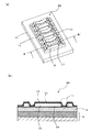
図7(a)は、MEMS素子30によって構成されるGLVデバイスの構造を説明する斜視図であり、図7(b)はMEMS素子の構造を示すA−A´断面の要部拡大図である。
図7(a)に示すように、GLVデバイスは複数個のMEMS素子30が並列して密に配置されたデバイスであり、このMEMS素子30は、上面に光反射面を有する静電駆動型のビーム13を備えた、MOEMS(Micro Optical Electro−Mechanical Systems)と称されているものである。
このようなMEMS素子30からなるGLVデバイスは、共通基板である基板10と、共通電極である下部電極14とを備え、下部電極14上に並列されブリッジ状に配置された複数のビーム13とビーム13の表面に形成された上部電極12とを備えている。
【0005】
ここで、図7(b)の断面図に示すように、このMEMS素子30におけるビーム13は、その端部が下部電極14上に保護膜22を介して配置されたブリッジ形状に形成されており、その表面には光反射膜としての機能も有する上部電極12が形成されている。
ビーム13は下部電極14に対向して所定間隔の空隙部15を有した状態で、下部電極14に対して平行に上部電極12を支持するものである。
ビーム13表面の上部電極12と下部電極14とは、この間に設けられた空隙部15、保護膜22およびビーム13により電気的に絶縁されている。
【0006】
このビーム13の端部の内側にはビーム13と一体で形成された支持部17が下部電極14上に保護膜22を介して立設されており、この支持部17はブリッジ状のビーム13を下部電極14側から支持している。
支持部17はビーム13の高さやビーム13を駆動させた場合の可動部分の長さおよび位置を規定するために形成され、支持部17を形成せずにビーム13の端部で支持するよりも共振周波数等の機械特性を安定させることができる。
【0007】
このようなMEMS素子30は、下部電極14とビーム13表面側の上部電極12との間に電圧を印加すると、図7(a)に示すように、静電現象によって支持部17よりも内側のビーム13が下部電極14に向かって接近し、また、電圧の印加を停止すると、離間して元の状態に戻る。
GLVデバイスはこのようなMEMS素子30が並列して複数配置されており、下部電極14に対するビーム13の接近、離間の動作により、上部電極12の高さを変えて、回折格子を形成し、反射する光の強度を変調して光変調素子として機能する。
【0008】
次に、上述したようなGLVデバイスに用いられるMEMS素子の製造方法を図8、図9の製造工程断面図を用いて説明する。
まず始めに、図8(a)に示すように、例えばシリコン基板(Si基板)からなる基板20上に例えば酸化シリコン(SiO2)からなる絶縁膜21を形成する。その後、絶縁膜21上に下部電極14を形成する。下部電極14にはタングステン(W)、クロム(Cr)等の高融点金属や多結晶シリコン(Poly−Si)が用いられる。
【0009】
次に、図8(b)に示すように、下部電極14の表面に酸化膜からなる保護膜22を形成する。この保護膜22は後述する工程で犠牲層を除去する際の保護膜として機能する。
そして、図8(c)に示すように、保護膜22上に例えばa−Si膜またはPoly−Si膜からなる犠牲層23を形成し、レジストパターン(図示せず)をマスクに用いて、下部電極14の形成領域よりも内側に犠牲層23が形成されるようにパターニングするとともに、後述する工程でビームの支持部を形成する領域の犠牲層23に、保護膜22に達する開口パターン23bを形成する。
【0010】
次に、図8(d)に示すように、この犠牲層23を覆うように保護膜22上に例えばSiN膜からなるビーム材料層を成膜し、開口パターン23bを含んだ帯状にパターニングする。これにより、保護膜22との間に犠牲層23を有したブリッジ形状のビーム13を形成するとともに、開口部23bの内壁に沿って保護膜22上にビーム13と一体に形成された支持部17を形成する。
続いて、図9(e)に示すように、ビーム13の表面に例えばAlからなる上部電極12を形成する。
【0011】
次に、図9(f)に示すように、犠牲層23(前記図9(e)参照)をビーム13および保護膜22に対して選択的に除去することにより、ビーム13と保護膜22との間に空隙部15を形成する。
これにより、下部電極14上に保護膜22を介して支持部17が立設され、ブリッジ形状のビーム13はこの支持部17によって支持される。
【0012】
このようにして、絶縁膜21上に形成された下部電極14と、下部電極14上に保護膜22を介してブリッジ状に形成され、並列して配置された複数のビーム13と複数のビーム13の表面に形成された上部電極12とを備えたMEMS素子30からなるGLVデバイスを製造する。
【0013】
【発明が解決しようとする課題】
しかしながら、図10の要部拡大図に示すように、上述した製造方法では、下部電極14の表面に凹凸が存在していると、レンズ効果によって凸部41の幅が拡大されていき、結果として上部電極12の表面に大きな凸部41aが形成される。このような凹凸の制御には下部電極の形成方法や形成後の温度履歴のコントロールが必要であった。
【0014】
ビーム13における支持部17の下部に凸部41が発生した場合、この上にビーム13および上部電極12を順次形成すると、凸部41の拡大により、凸部41上に形成された支持部17の高さが部分的に短くなり、この部分の支持部17の強度が強くなるという現象が生じていた。特に、下部電極14と上部電極12間に電圧を印加して、ビーム13を下部電極14側に接近させた場合は、支持部17間に引っ張り応力が生じることから、支持部17の強度が部分的に変化することにより、ビーム13の変形具合が変化したり、ビーム13にねじれが発生したりするという問題があった。
【0015】
GLVデバイスにおける一部のMEMS素子30のビーム13で上記のように支持部17の強度が部分的に変化すると、ビーム13表面の光反射膜も兼ねた上部電極12によって形成される回折格子による回折光の強度が変化することとなるため、コントラストが悪化し、光学デバイスとしての特性を十分に満たせなくなるという課題があった。
【0016】
本発明は上述したようにビームの支持部の高さを均一にすることで、支持部の強度を均一にし、ディスプレイ表示装置としての特性を向上させるマイクロマシンおよびその製造方法を提供する。
【0017】
【課題を解決するための手段】
上記のような課題を解決するために、本発明のマイクロマシンは、基板上に形成された下部電極と、下部電極との間に空隙を有して配設されたビームと、ビームの表面に形成された上部電極とを備えたマイクロマシンにおいて、下部電極は基板に達する開口パターンを有し、この開口パターン内の基板上にビームの支持部が立設されていることを特徴としている。
【0018】
このようなマイクロマシンによれば、ビームの支持部が下部電極に形成された開口パターン内の基板上に立設されていることから、下部電極の表面に凹凸があったとしても、この凹凸の影響を受けることなく、ビームの支持部の高さを均一にすることができる。このため、支持部の強度を均一にすることができる。
したがって、このようなマイクロマシンに電圧を印加して、上部電極が形成されたビームを下部電極側に接近させた場合でも、ビームの変形具合が変化したり、ビームにねじれが生じたりすることなく、変形時のビームの高さを制御することができる。
【0019】
また、本発明におけるマイクロマシンの第1の製造方法は、基板上に第1の開口パターンを有する下部電極を形成する工程と、下部電極を覆うように前記基板上に犠牲層を形成する工程と、犠牲層を下部電極と重なるようにパターニングするとともに、第1の開口パターン上の犠牲層に基板に達する第2の開口パターンを形成する工程と、犠牲層を覆うように基板上にビーム材料層を成膜した後、第2の開口パターンを含んだ帯状にビーム材料層をパターニングすることによって、下部電極上に犠牲層を介してビームを形成するとともに、第2の開口パターン内の基板上にビームと一体に形成された支持部を形成する工程と、ビームの表面に上部電極を形成する工程と、犠牲層を除去することによって、下部電極とビームとの間に空隙を設けるとともに支持部を第1の開口パターン内の基板上に立設することを特徴としている。
【0020】
このようなマイクロマシンの製造方法によれば、下部電極における第1の開口パターン上の犠牲層に形成した第2の開口パターン内の基板上にビームの支持部が形成される。そして、犠牲層を除去することにより、ビームの支持部が第1の開口パターン内の基板上に立設される。これにより、下部電極の表面に凹凸が形成されたとしても、ビームの支持部は基板上に立設されるため、凹凸の影響を受けることなくビームの支持部を形成することができる。よって、ビームの支持部の高さを均一にすることができ、支持部の強度を均一にすることができる。
【0021】
また、本発明におけるマイクロマシンの第2の製造方法によれば、基板上に下部電極を形成する工程と、下部電極上に犠牲層を形成した後、マスクパターンをマスクに用いて、犠牲層および下部電極をパターニングするとともに、この犠牲層および下部電極に基板に達する開口パターンを形成する工程と、パターニングされた犠牲層および下部電極を覆うように、基板上にビーム材料層を成膜した後、開口パターンを含んだ帯状にパターニングすることによって、下部電極上に犠牲層を介してビームを形成するとともに、開口パターン内の基板上にビームと一体に形成された支持部を形成する工程と、ビームの表面に上部電極を形成する工程と、犠牲層を除去して下部電極とビームとの間に空隙を設けるともに支持部を開口パターン内の基板上に立設する工程とを有することを特徴としている。
【0022】
このようなマイクロマシンの製造方法によれば、犠牲層および下部電極に基板に達する開口パターンを形成し、開口パターン内の基板上にビームの支持部を形成して犠牲層を除去することにより、ビームの支持部が開口パターン内の基板上に立設されることから、上述した第1の製造方法と同様の効果を奏する。
また、この方法によれば、支持部の基板側は開口パターンの内壁の一部である下部電極で支持された状態となる。これにより、支持部をより安定的に形成することができる。
さらに、犠牲層および下部電極を同一工程で除去して開口パターンを形成することから、第1の開口パターンおよび第2の開口パターンを形成する第1の製造方法よりも工程負荷の大きいリソグラフィ工程が少なく、生産性により優れている。
【0023】
【発明の実施の形態】
(第1実施形態)
本発明における第1実施形態のマイクロマシン(以下、MEMS素子31とする)の断面図を図1に示す。本実施形態では例えばGLVデバイスに用いられるMEMS素子31について説明する。
従来の技術と同一の構成要素には同一の番号を付して説明する。
本実施形態におけるMEMS素子31は絶縁膜21が形成された基板20と、絶縁膜21上に形成された下部電極14と、絶縁膜21上にブリッジ状に形成されたビーム13と、ビーム13の表面に形成された上部電極12とから構成される。
【0024】
図1に示すように、基板20は例えばシリコン基板からなり、その上には例えばSiO2からなる絶縁膜21が形成されている。
ここで、基板20から絶縁膜21までが請求項1記載の基板に相当する。
また、下部電極14は例えばW、Cr等の高融点金属またはPoly−Siからなり絶縁膜21上に形成されている。下部電極14はその端部側に絶縁膜21に達する第1の開口パターン14aを有し、下部電極14の表面は酸化膜からなる保護膜22で覆われている。
【0025】
ビーム13は例えばSiNからなり、その端部は下部電極14の外側の絶縁膜21上に配置され、ブリッジ形状に形成されている。また、ビーム13の表面には光反射膜としての機能も有する例えばAlからなる上部電極12が形成されている。
ビーム13表面の上部電極12と下部電極14とは、この間に設けられた空隙部15、保護膜22およびビーム13によって電気的に絶縁されており、ビーム13は下部電極14に対向して所定間隔の空隙部15を有して配置され、下部電極14に対して平行に上部電極12を支持している。
【0026】
このビーム13の支持部17はビーム13と一体に形成され、下部電極14における第1の開口パターン14a内の絶縁膜21上に第1の開口パターン14aの内壁から離間した状態で立設されている。
なお、ここでは支持部17が下部電極14を覆う保護膜22から離間した状態で立設されていることとしたが、第1の開口パターン14a内の絶縁膜21上に立設されていれば、保護膜22と接していてもよい。
また、ここではビーム13の端部が絶縁膜21上に配置されることとしたが、本発明はこれに限定されず、支持部17が絶縁膜21上に配置されていればよく、その端部は保護膜22を介した下部電極14上に配置されていてもよい。
【0027】
このようなマイクロマシンによれば、ビーム13の支持部17が第1の開口パターン14a内の絶縁膜21上に立設されている。これにより、下部電極14の表面に凹凸のある場合でも、ビーム13の支持部17は絶縁膜21上に配置されており、SiO2からなる絶縁膜21の表面は高融点金属またはPoly−Siからなる下部電極14の表面と比較して凹凸が少ないことから、支持部17が下部電極14上に保護膜22を介して立設される場合と比較して、支持部17の高さを均一にすることができ、これにより支持部17の強度を均一にすることができる。
【0028】
したがって、このようなMEMS素子31に電圧を印加して、ビーム13を下部電極14側に接近させた場合に、支持部17の強度を均一にできるので、ビーム13の変形具合が変化したり、ビーム13にねじれが生じたりすることなく、ビーム13の変形時の高さを制御することができる。
また、このようなMEMS素子31が用いられたGLVデバイスでは複数のビーム13の支持部17の強度を均一にすることができるため、ビーム13表面の上部電極12により形成される回折格子による回折光の強度をより確実に制御することが可能である。
【0029】
上述したようなMEMS素子は例えば次のような方法により製造することができる。本実施形態においてはGLVデバイスに用いられるMEMS素子の製造方法を例にとって説明する。
図2〜図3に本実施形態におけるMEMS素子の製造工程断面図を示す。
【0030】
まず始めに、図2(a)に示すように、例えばシリコン基板からなる半導体基板20上に絶縁膜21を成膜する。
その後、絶縁膜21上に、例えば高融点金属膜またはPoly−Si膜からなる下部電極14を形成し、レジストパターン(図示せず)をマスクに用いて、絶縁膜21よりも内側に下部電極14が形成されるようにパターニングする。また、後述する工程でビームの支持部を形成する領域の下部電極14に、絶縁膜21に達するとともに支持部の径よりも大きい径の第1の開口パターン14aを形成する。
【0031】
次に、図2(b)に示すように、下部電極14の表面に例えばSiO2からなる保護膜22を形成する。この保護膜22は後述する工程で犠牲層を除去する際に下部電極14を保護するために形成するものであり、犠牲層を除去する際に下部電極14に影響を与えることなく犠牲層を選択的に除去することができれば、保護膜22を形成しなくてもよい。
【0032】
次に、図2(c)に示すように、保護膜22を覆うように絶縁膜21上に例えばa−Si膜またはPoly−Si膜からなる犠牲層23を成膜する。そして、レジストパターンをマスクに用いて、例えば下部電極14よりも内側に形成されるように犠牲層23をパターニングするとともに、第1の開口パターン14a上の犠牲層23に、絶縁膜21に達する第2の開口パターン23aを形成する。
この第2の開口パターン23aの径が後述する工程で形成するビームの支持部の径となることから、ビームを支持可能な強度を有する径に適宜設定する。
【0033】
なお、ここでは犠牲層23が下部電極14よりも内側に形成されるように犠牲層23をパターニングすることとしたが、本発明はこれに限定されず、犠牲層23が下部電極14と重なるように形成されていればよい。
また、後述する工程で犠牲層23をこの上に形成するビームと保護膜22および絶縁膜21に対して選択的にエッチング除去することから、犠牲層23はビームと保護膜22および絶縁膜21に対してエッチング選択比の高い材質で形成する。
なお、保護膜22を形成しない場合には、犠牲層23をビームと下部電極14および絶縁膜21に対して選択的にエッチング除去することから、これらに対してエッチング選択比の高い材料を適宜選択して形成する。
【0034】
続いて、図2(d)に示すように、例えば化学的気相成長(Chemical Vapor Deposition(CVD))法により犠牲層23および保護膜22を覆うように、絶縁膜21上に、例えばSiN膜からなるビーム材料層(図示せず)を成膜する。このとき第2の開口パターン23aの内壁もビーム材料層で覆うように成膜する。
ここで、ビーム13の力学的特性は成膜するビーム材料層の物性によって決定する。本実施形態で用いるSiN膜はその強度、弾性定数等の物性値がビーム13の機械的駆動に対して適切であり、好ましい。
【0035】
そして、レジストパターンをマスクに用いて、第2の開口パターン23aを含んだ帯状にビーム材料層をパターニングすることによって、保護膜22との間に犠牲層23を有したブリッジ形状の複数のビーム13を並列させた状態で形成する。
また、第2の開口パターン23aの内壁に沿って、絶縁膜21上にビーム13と一体に形成されたビーム13の支持部17を形成する。
【0036】
次いで、ここでの図示を省略したがビーム13の端部に配線用Alを成膜し、パターニングする。
ここではビーム13の端部を絶縁膜21上に形成したが、本発明はこれに限定されず、支持部17が絶縁膜21上に形成されていればよく、その端部は保護膜22上に形成されていてもよい。
【0037】
次に、図3(e)に示すように、例えばAlからなる導電性膜を、ビーム13を覆うように犠牲層23上に成膜し、パターニングすることにより、ビーム13の表面に上部電極12を形成する。
ここで、Alは比較的容易に成膜でき、可視光領域での光反射率の波長分散が小さく、また、Al表面に生成したアルミナ自然酸化膜が保護膜となって反射面を保護するため、光反射膜も兼ねた上部電極12の材質として好ましい。
ここでは、ビーム材料層をパターニングしてビーム13を形成した後、導電性膜を成膜し、パターニングすることで上部電極12を形成したが、ビーム材料層を成膜した後導電性膜を成膜し、ビーム13と上部電極12とをパターニングしてもよい。
【0038】
そして、図3(f)に示すように、犠牲層23(前記図3(e)参照)をフッ化キセノン(XeF2)ガスを用いたドライエッチング法により除去する。これにより、保護膜22とビーム13との間に空隙部15を形成するとともに、支持部17を第1の開口パターン14a内の絶縁膜21上に第1の開口パターン14aの内壁から離間した状態で立設する。
そして、ブリッジ形状のビーム13はこの支持部17によって支持される。
【0039】
このようにして、絶縁膜21上に形成された下部電極14と、絶縁膜21上にブリッジ状に形成され、下部電極14における第1の開口パターン14a内の絶縁膜21上に立設された支持部17を有する複数のビーム13と複数のビーム13の表面に形成された上部電極12とを備えたMEMS素子31からなるGLVデバイスを製造する。
【0040】
このようなMEMS素子31の製造方法によれば、ビーム13の支持部17は保護膜22を介した下部電極14上ではなく、第1の開口パターン14a内の絶縁膜21上に立設される。
これにより、下部電極14の表面に凹凸が形成されたとしても、下部電極14の表面と比較して凹凸の少ないSiO2からなる絶縁膜21上に支持部17を立設することから、支持部17の高さを均一に形成することができ、その強度を均一にすることができる。
【0041】
なお、本実施形態においては支持部17を絶縁膜21上に形成したが、第1の開口パターン14aの底部に露出した絶縁膜21を除去して、基板20に達する開口パターンを形成し、支持部17をこの開口パターン内の基板20上に形成してもよい。支持部17を基板20上に形成しても、上記と同様の効果を奏することができる。
この場合は下部電極14の第1の開口パターン14aを形成する際に用いたレジストパターンをマスクに用いたエッチングにより絶縁膜21を除去してもよく、下部電極14をマスクに用いて絶縁膜21を除去してもよい。
さらに、第1の開口パターン14aを形成した後、新たなレジストパターンを用いて第1の開口パターン14a以外の下部電極14および絶縁膜21上を覆い、第1の開口パターン14aの底部に露出した絶縁膜21のみを除去してもよい。
【0042】
(第2実施形態)
本発明における第2実施形態のマイクロマシン(以下MEMS素子32とする)の断面図を図4に示す。本実施形態では、例えばGLVデバイスに用いられるMEMS素子32について説明する。
第1実施形態と同一の構成要素には同一の番号を付し、その詳細な説明は省略する。
本実施形態におけるMEMS素子32は絶縁膜21が形成された基板20と、絶縁膜21上に形成された下部電極14と、絶縁膜21上にブリッジ状に設けられたビーム13と、ビーム13の表面に設けられた上部電極12とから構成される。
【0043】
基板20上には絶縁膜21が形成されており、絶縁膜21上には下部電極14が配置されている。
下部電極14はその端部側に絶縁膜21に達する開口パターン24aを有し、下部電極14の表面は酸化膜からなる保護膜22で覆われている。
【0044】
ビーム13はその端部が下部電極14の外側の絶縁膜21上に配置され、保護膜22との間に空隙部15を有してブリッジ形状に設けられている。また、ビーム13の表面には光反射膜も兼ねた上部電極12が形成されている。
ビーム13表面の上部電極12と下部電極14とは、この間に設けられた空隙部15、保護膜22およびビーム13により電気的に絶縁されている。
【0045】
このビーム13の支持部17はビーム13と一体に形成され、下部電極14における第1の開口パターン24a内の絶縁膜21上に立設されている。支持部17は絶縁膜21側が開口パターン24aの内壁で支持されている。
【0046】
このようなMEMS素子32によれば、ビーム13の支持部17が絶縁膜21上に配置されていることから、第1実施形態のMEMS素子31と同様の効果を奏することができる。
さらに、この支持部17の絶縁膜21側は開口パターン24aの内壁で支持されていることから、支持部17をより安定させることができる。
【0047】
本発明における第2実施形態のMEMS素子32の製造方法を図5〜図6の製造工程断面図に示す。
まず始めに、図5(a)に示すように、基板20上に絶縁膜21を形成し、絶縁膜21上に下部電極14を形成する。
次に、図5(b)に示すように、下部電極14の表面に保護膜22として酸化膜を形成する。
【0048】
続いて、図5(c)に示すように、保護膜22上に犠牲層23を形成し、レジストパターン(図示せず)をマスクに用いて、犠牲層23、保護膜22および下部電極14を絶縁膜21よりも内側に形成されるようにパターニングするとともに、後述する工程でビームの支持部を形成する領域の犠牲層23、保護膜22および下部電極14に、絶縁膜21に達する開口パターン24を形成する。
ここで、開口パターン24の径が後述する工程で形成するビームの支持部の径となることから、ビームを支持可能な強度を有する径に適宜設定する。
【0049】
続いて、図5(d)に示すように、パターニングされた下部電極14、保護膜22および犠牲層23を覆うように絶縁膜21上にビーム材料層(図示せず)を成膜する。このとき開口パターン24の内壁もビーム材料層で覆うように成膜する。
そして、レジストパターンをマスクに用いて、開口パターン24を含んだ帯状にビーム材料層をパターニングすることによって、保護膜22との間に犠牲層23を有したブリッジ形状の複数のビーム13を形成する。
また、開口パターン24の内壁に沿って絶縁膜21上にビーム13と一体に形成されたビーム13の支持部17を形成する。
【0050】
次いで、ここでの図示を省略するが、ビーム13の端部に配線用Alを成膜してパターニングし、そして図6(e)に示すように、ビーム13を覆うように例えばAlからなる導電性膜を犠牲層23上に成膜し、パターニングすることによりビーム13の表面に光反射膜を兼ねた上部電極12を形成する。
【0051】
そして、図6(f)に示すように、犠牲層23(前記図6(e)参照)をドライエッチングにより除去する。これにより保護膜22とビーム13との間に空隙部15が形成され、開口パターン24(前記図6(e)参照)もその上部が除去された状態となり、内壁が保護膜22と下部電極14とで形成される開口パターン24aとなる。
また、ビーム13の支持部17は開口パターン24a内の絶縁膜21上に開口パターン24aの内壁に支持された状態で立設される。
【0052】
このようにして、絶縁膜21上に形成された下部電極14と、絶縁膜21上にブリッジ状に形成され、下部電極14における開口パターン24a内の絶縁膜21上に立設された支持部17を有する複数のビーム13と複数のビーム13の表面に形成された上部電極12とを備えたMEMS素子32からなるGLVデバイスを製造する。
【0053】
このようなMEMS素子32の製造方法によれば、ビーム13の支持部17を保護膜22を介した下部電極14上ではなく、開口パターン24a内の絶縁膜21上に形成する。これにより、第1実施形態で説明した製造方法と同様の効果を奏する。
また、犠牲層23、保護膜22および下部電極14に絶縁膜21に達する開口パターン24を形成し、開口部パターン24の内壁に沿って絶縁膜21上に支持部17を形成した後、犠牲層23を除去することから、支持部17の絶縁膜21側は、保護膜22および下部電極14からなる開口部パターン24aの内壁で支持された状態となる。これにより、支持部17をより安定的に形成することができる。
さらに、犠牲層23、保護膜22および下部電極14を同一工程で除去して開口パターン24を形成することから、第1実施形態で説明した製造方法よりも工程負荷の大きいリソグラフィ工程が少なく、生産性により優れている。
【0054】
なお、上述した実施形態においては、ブリッジ形状のビーム13を備えたMEMS素子に本発明を適用した場合を説明した。しかし、本発明はブリッジ形状のビーム13に換えて、ビーム13の一方の端部側のみに支持部17が形成されたカンチレバー式の構成のビームを有するMEMS素子にも同様に適用可能である。
【0055】
【発明の効果】
以上説明したように、本発明のマイクロマシンによれば、ビームの支持部が基板上に配置されることから、下部電極の表面に凹凸があったとしても、この凹凸の影響を受けることなく、ビームの支持部の高さを均一にすることができるため、支持部の強度を均一にすることができる。
したがって、このようなマイクロマシンに電圧を印加して、ビームを下部電極側に接近させた場合でも、支持部の強度が均一であることから、ビームの変形具合が変化したり、ビームにねじれが生じたりすることなく、ビームの変形時の高さを制御することができる。
また、このようなマイクロマシンが複数並列して配置されたGLVでは、各マイクロマシンにおけるビームの支持部の強度を均一にし、マイクロマシンに電圧を印加した場合の各ビームにおける変形時の高さを制御できるので、ビーム表面の上部電極により形成される回折格子による回折光の強度をより確実に制御することが可能となる。
【0056】
また、本発明のマイクロマシンの第1の製造方法によれば、ビームの支持部を第1の開口パターン内の基板上に立設することから、下部電極の表面に凹凸が発生したとしても、ビームの支持部の高さを均一にすることができ、支持部の強度を均一にすることができる。
【0057】
また、本発明のマイクロマシンの第2の製造方法によれば、開口パターン内の基板上にビームの支持部を立設することから、第1の製造方法と同様の効果を奏することが可能である。
さらに、この方法によれば、支持部の基板側は開口パターンの内壁の一部である下部電極で支持されることから、支持部をより安定的に形成することができる。
また、犠牲層および下部電極を同一工程で除去して開口パターンを形成することから、第1の製造方法よりも工程負荷の大きいリソグラフィ工程が少なく、生産性により優れている。
【図面の簡単な説明】
【図1】第1実施形態におけるマイクロマシンを説明するための断面図である。
【図2】第1実施形態におけるマイクロマシンの製造方法を説明するための製造工程断面図(その1)である。
【図3】第1実施形態におけるマイクロマシンの製造方法を説明するための製造工程断面図(その2)である。
【図4】第2実施形態におけるマイクロマシンを説明するための断面図である。
【図5】第2実施形態におけるマイクロマシンの製造方法を説明するための製造工程断面図(その1)である。
【図6】第2実施形態におけるマイクロマシンの製造方法を説明するための製造工程断面図(その2)である。
【図7】従来の技術におけるマイクロマシンを説明するための斜視図(a)、断面図(b)である。
【図8】従来の技術におけるマイクロマシンの製造方法を説明するための製造工程断面図(その1)である。
【図9】従来の技術におけるマイクロマシンの製造方法を説明するための製造工程断面図(その2)である。
【図10】従来の技術における課題を示す断面図である。
【符号の説明】
12…上部電極、13…ビーム、14…下部電極、14a…第1の開口パターン、23a…第2の開口パターン、24,24a…開口パターン、17…支持部、20…基板、21…絶縁膜、22…保護膜、23…犠牲層、31,32…MEMS素子[0001]
TECHNICAL FIELD OF THE INVENTION
The present invention relates to a micromachine and a method for manufacturing the same, and more particularly, to a light modulation element for interfering, diffracting, and modulating light applied to a GLV (Grating Light Valve) device and the like, and a method for manufacturing the same.
[0002]
[Prior art]
2. Description of the Related Art With the development of microtechnology, a so-called micro-electro-mechanical system (MEMS) element (hereinafter, referred to as a MEMS element) has attracted attention.
The MEMS element is formed as a fine structure on a substrate such as a silicon substrate or a glass substrate, and electrically connects a driving body that outputs a mechanical driving force, a semiconductor integrated circuit that controls the driving of the driving body, and the like. These are elements that are mechanically connected. The basic feature of the MEMS element is that a driving body configured as a mechanical structure is incorporated in a part of the element, and the driving output of the driving body applies Coulomb attraction between electrodes and the like. It is generally performed electrically.
[0003]
As an example of the MEMS element, a structure of a GLV (Grating Light Valve) device developed as an optical modulator will be described as an example.
[0004]
FIG. 7A is a perspective view for explaining the structure of a GLV device constituted by the
As shown in FIG. 7A, the GLV device is a device in which a plurality of
The GLV device including such a
[0005]
Here, as shown in the cross-sectional view of FIG. 7B, the
The
The
[0006]
Inside the end of the
The
[0007]
When a voltage is applied between the
In the GLV device, a plurality of
[0008]
Next, a method of manufacturing the MEMS element used in the above-described GLV device will be described with reference to the manufacturing process sectional views of FIGS.
First, as shown in FIG. 8A, for example, silicon oxide (SiO 2) is formed on a
[0009]
Next, as shown in FIG. 8B, a
Then, as shown in FIG. 8C, a
[0010]
Next, as shown in FIG. 8D, a beam material layer made of, for example, a SiN film is formed on the
Subsequently, as shown in FIG. 9E, the
[0011]
Next, as shown in FIG. 9F, the
Thus, the
[0012]
In this way, the
[0013]
[Problems to be solved by the invention]
However, as shown in the main part enlarged view of FIG. 10, in the above-described manufacturing method, if there is unevenness on the surface of the
[0014]
When the
[0015]
When the intensity of the
[0016]
The present invention provides a micromachine and a method for manufacturing the same, in which the height of the support portion of the beam is made uniform as described above, thereby making the strength of the support portion uniform and improving the characteristics as a display device.
[0017]
[Means for Solving the Problems]
In order to solve the problems described above, a micromachine of the present invention includes a lower electrode formed on a substrate, a beam disposed with a gap between the lower electrode, and a beam formed on a surface of the beam. In the micromachine provided with the upper electrode and the upper electrode, the lower electrode has an opening pattern reaching the substrate, and a beam supporting portion is erected on the substrate in the opening pattern.
[0018]
According to such a micromachine, since the beam supporting portion is erected on the substrate in the opening pattern formed in the lower electrode, even if there is unevenness on the surface of the lower electrode, the influence of the unevenness is not significant. The height of the supporting portion of the beam can be made uniform without receiving the beam. For this reason, the strength of the support portion can be made uniform.
Therefore, even when a voltage is applied to such a micromachine and the beam on which the upper electrode is formed is brought closer to the lower electrode side, the deformation state of the beam does not change, and the beam is not twisted. The height of the beam at the time of deformation can be controlled.
[0019]
Also, a first method of manufacturing a micromachine according to the present invention includes a step of forming a lower electrode having a first opening pattern on a substrate; and a step of forming a sacrificial layer on the substrate so as to cover the lower electrode. Patterning the sacrificial layer so as to overlap the lower electrode, forming a second opening pattern reaching the substrate in the sacrificial layer on the first opening pattern, and forming a beam material layer on the substrate so as to cover the sacrificial layer. After forming the film, the beam is formed on the lower electrode via the sacrificial layer by patterning the beam material layer into a band shape including the second opening pattern, and the beam is formed on the substrate in the second opening pattern. Forming a support unit integrally formed with the beam, forming an upper electrode on the surface of the beam, and providing a gap between the lower electrode and the beam by removing the sacrificial layer. It is characterized by erecting the support portion on the substrate of first opening patterns with.
[0020]
According to such a micromachine manufacturing method, the beam support is formed on the substrate in the second opening pattern formed in the sacrificial layer on the first opening pattern in the lower electrode. Then, by removing the sacrificial layer, the beam supporting portion is set up on the substrate in the first opening pattern. Thus, even if irregularities are formed on the surface of the lower electrode, the beam supporting portions are erected on the substrate, so that the beam supporting portions can be formed without being affected by the irregularities. Therefore, the height of the beam support portion can be made uniform, and the strength of the support portion can be made uniform.
[0021]
According to the second method for manufacturing a micromachine of the present invention, a step of forming a lower electrode on a substrate, a step of forming a sacrificial layer on the lower electrode, and then using a mask pattern as a mask, Patterning the electrode and forming an opening pattern reaching the substrate in the sacrificial layer and the lower electrode; forming a beam material layer on the substrate so as to cover the patterned sacrificial layer and the lower electrode; Forming a beam through the sacrificial layer on the lower electrode by patterning into a strip shape including the pattern, and forming a support unit integrally formed with the beam on the substrate in the opening pattern; and Forming an upper electrode on the surface, removing the sacrificial layer to provide a gap between the lower electrode and the beam, and supporting the substrate in the opening pattern It is characterized by a step of erected.
[0022]
According to the manufacturing method of such a micromachine, an opening pattern reaching the substrate is formed in the sacrificial layer and the lower electrode, and a beam support is formed on the substrate in the opening pattern to remove the sacrificial layer. Are erected on the substrate in the opening pattern, so that the same effects as those of the first manufacturing method described above can be obtained.
Further, according to this method, the substrate side of the support portion is supported by the lower electrode that is a part of the inner wall of the opening pattern. Thereby, the support portion can be formed more stably.
Further, since the sacrificial layer and the lower electrode are removed in the same step to form the opening pattern, a lithography step having a higher process load than the first manufacturing method of forming the first opening pattern and the second opening pattern is required. Less, better in productivity.
[0023]
BEST MODE FOR CARRYING OUT THE INVENTION
(1st Embodiment)
FIG. 1 is a cross-sectional view of a micromachine (hereinafter, referred to as a MEMS element 31) according to a first embodiment of the present invention. In the present embodiment, for example, a MEMS element 31 used for a GLV device will be described.
The same components as those of the related art will be described with the same reference numerals.
The MEMS element 31 according to the present embodiment includes a
[0024]
As shown in FIG. 1, the
Here, the portion from the
The
[0025]
The
The
[0026]
The
Here, it is assumed that the
In addition, although the end of the
[0027]
According to such a micromachine, the
[0028]
Therefore, when a voltage is applied to such a MEMS element 31 to bring the
Further, in the GLV device using such a MEMS element 31, the intensity of the
[0029]
The MEMS element as described above can be manufactured, for example, by the following method. In the present embodiment, a method for manufacturing a MEMS element used for a GLV device will be described as an example.
2 to 3 are cross-sectional views illustrating a manufacturing process of the MEMS device according to the present embodiment.
[0030]
First, as shown in FIG. 2A, an insulating
Thereafter, a
[0031]
Next, as shown in FIG. 2 Is formed. The
[0032]
Next, as shown in FIG. 2C, a
Since the diameter of the
[0033]
Here, the
In addition, the
If the
[0034]
Subsequently, as shown in FIG. 2D, for example, a SiN film is formed on the insulating
Here, the mechanical properties of the
[0035]
Then, by using the resist pattern as a mask and patterning the beam material layer into a band shape including the
Further, along the inner wall of the
[0036]
Next, although not shown here, Al for wiring is formed at the end of the
Here, the end of the
[0037]
Next, as shown in FIG. 3E, a conductive film made of, for example, Al is formed on the
Here, Al can be formed relatively easily, the wavelength dispersion of light reflectance in the visible light region is small, and the natural alumina oxide film formed on the Al surface serves as a protective film to protect the reflective surface. It is preferable that the
Here, after forming the
[0038]
Then, as shown in FIG. 3 (f), the sacrificial layer 23 (see FIG. 3 (e)) is changed to xenon fluoride (XeF). 2 ) Removed by dry etching using gas. As a result, a
The bridge-shaped
[0039]
In this way, the
[0040]
According to such a method of manufacturing the MEMS element 31, the
As a result, even if irregularities are formed on the surface of the
[0041]
In the present embodiment, the
In this case, the insulating
Furthermore, after forming the
[0042]
(2nd Embodiment)
FIG. 4 is a sectional view of a micro machine (hereinafter, referred to as a MEMS element 32) according to a second embodiment of the present invention. In the present embodiment, for example, a
The same components as those of the first embodiment are denoted by the same reference numerals, and detailed description thereof will be omitted.
The
[0043]
An insulating
The
[0044]
The end of the
The
[0045]
The
[0046]
According to such a
Furthermore, since the insulating
[0047]
A method of manufacturing the
First, as shown in FIG. 5A, an insulating
Next, as shown in FIG. 5B, an oxide film is formed as a
[0048]
Subsequently, as shown in FIG. 5C, a
Here, since the diameter of the
[0049]
Subsequently, as shown in FIG. 5D, a beam material layer (not shown) is formed on the insulating
Then, by using the resist pattern as a mask and patterning the beam material layer into a band including the
Further, a
[0050]
Next, although not shown here, Al for wiring is formed at the end of the
[0051]
Then, as shown in FIG. 6F, the sacrificial layer 23 (see FIG. 6E) is removed by dry etching. As a result, a
The
[0052]
In this way, the
[0053]
According to such a method of manufacturing the
Further, an
Further, since the
[0054]
In the above-described embodiment, the case where the present invention is applied to the MEMS element including the bridge-shaped
[0055]
【The invention's effect】
As described above, according to the micromachine of the present invention, since the beam support is disposed on the substrate, even if the surface of the lower electrode has irregularities, the beam is not affected by the irregularities. Since the height of the support portion can be made uniform, the strength of the support portion can be made uniform.
Therefore, even when a voltage is applied to such a micromachine and the beam is brought closer to the lower electrode, the strength of the supporting portion is uniform, so that the deformation of the beam changes or the beam is twisted. It is possible to control the height of the beam at the time of deformation without any trouble.
Further, in a GLV in which a plurality of such micromachines are arranged in parallel, the strength of the beam support in each micromachine can be made uniform, and the height of each beam when deformed when a voltage is applied to the micromachine can be controlled. In addition, the intensity of the diffracted light by the diffraction grating formed by the upper electrode on the beam surface can be more reliably controlled.
[0056]
Further, according to the first manufacturing method of the micromachine of the present invention, since the beam support is erected on the substrate in the first opening pattern, even if the surface of the lower electrode has irregularities, The height of the support portion can be made uniform, and the strength of the support portion can be made uniform.
[0057]
Further, according to the second manufacturing method of the micro machine of the present invention, since the beam support is erected on the substrate in the opening pattern, the same effect as in the first manufacturing method can be obtained. .
Further, according to this method, since the substrate side of the support portion is supported by the lower electrode that is a part of the inner wall of the opening pattern, the support portion can be formed more stably.
In addition, since the sacrificial layer and the lower electrode are removed in the same step to form an opening pattern, the number of lithography steps with a larger process load than in the first manufacturing method is small, and the productivity is superior.
[Brief description of the drawings]
FIG. 1 is a cross-sectional view illustrating a micro machine according to a first embodiment.
FIG. 2 is a manufacturing process cross-sectional view (part 1) for describing the method for manufacturing a micromachine in the first embodiment.
FIG. 3 is a manufacturing process sectional view (part 2) for describing the method for manufacturing the micromachine in the first embodiment.
FIG. 4 is a cross-sectional view illustrating a micro machine according to a second embodiment.
FIG. 5 is a cross-sectional view (part 1) illustrating a manufacturing process for illustrating a method for manufacturing a micromachine in the second embodiment.
FIG. 6 is a manufacturing process sectional view (part 2) for describing the method for manufacturing the micromachine in the second embodiment.
7A and 7B are a perspective view and a cross-sectional view for explaining a micromachine according to a conventional technique.
FIG. 8 is a cross-sectional view (No. 1) of a manufacturing process for describing a method of manufacturing a micromachine in a conventional technique.
FIG. 9 is a sectional view of a manufacturing process (part 2) for describing a method of manufacturing a micromachine in a conventional technique.
FIG. 10 is a cross-sectional view showing a problem in the related art.
[Explanation of symbols]
12 upper electrode, 13 beam, 14 lower electrode, 14a first opening pattern, 23a second opening pattern, 24, 24a opening pattern, 17 supporter, 20 substrate, 21 insulating film , 22 ... protective film, 23 ... sacrificial layer, 31, 32 ... MEMS element
Claims (6)
前記下部電極は前記基板に達する開口パターンを有し、この開口パターン内の前記基板上に前記ビームの支持部が立設されている
ことを特徴とするマイクロマシン。A lower electrode formed on a substrate, a beam disposed with a gap between the lower electrode, and a micro machine including an upper electrode formed on the surface of the beam,
The micromachine according to claim 1, wherein the lower electrode has an opening pattern reaching the substrate, and the beam support is erected on the substrate in the opening pattern.
ことを特徴とする請求項1記載のマイクロマシン。2. The micromachine according to claim 1, wherein a surface of the lower electrode is covered with a protective film.
前記下部電極を覆うように前記基板上に犠牲層を形成する工程と、
前記犠牲層を前記下部電極と重なるようにパターニングするとともに、前記第1の開口パターン上の前記犠牲層に前記基板に達する第2の開口パターンを形成する工程と、
前記犠牲層を覆うように前記基板上にビーム材料層を成膜した後、前記第2の開口パターンを含んだ帯状に前記ビーム材料層をパターニングすることによって、前記下部電極上に前記犠牲層を介してビームを形成するとともに、前記第2の開口パターン内の前記基板上に前記ビームと一体に形成された支持部を形成する工程と、
前記ビームの表面に上部電極を形成する工程と、
前記犠牲層を除去することによって、前記下部電極と前記ビームとの間に空隙を設けるとともに前記支持部を前記第1の開口パターン内の前記基板上に立設する
ことを特徴とするマイクロマシンの製造方法。Forming a lower electrode having a first opening pattern on the substrate;
Forming a sacrificial layer on the substrate to cover the lower electrode;
Patterning the sacrificial layer so as to overlap the lower electrode, and forming a second opening pattern reaching the substrate in the sacrificial layer on the first opening pattern;
After forming a beam material layer on the substrate so as to cover the sacrificial layer, by patterning the beam material layer into a band including the second opening pattern, the sacrificial layer is formed on the lower electrode. Forming a beam on the substrate in the second opening pattern and forming a support unit integrally formed with the beam,
Forming an upper electrode on the surface of the beam;
Removing the sacrificial layer, thereby providing a gap between the lower electrode and the beam, and erecting the support on the substrate in the first opening pattern. Method.
ことを特徴とする請求項3記載のマイクロマシンの製造方法。4. The method according to claim 3, wherein a step of forming a protective film on a surface of the lower electrode is performed before forming the sacrificial layer.
前記下部電極上に犠牲層を形成した後、マスクパターンをマスクに用いて、前記犠牲層および前記下部電極をパターニングするとともに、この犠牲層および下部電極に前記基板に達する開口パターンを形成する工程と、
パターニングされた前記犠牲層および前記下部電極を覆うように、前記基板上にビーム材料層を成膜した後、前記開口パターンを含んだ帯状にパターニングすることによって、前記下部電極上に前記犠牲層を介してビームを形成するとともに、前記開口パターン内の前記基板上に前記ビームと一体に形成された支持部を形成する工程と、
前記ビームの表面に上部電極を形成する工程と、
前記犠牲層を除去して前記下部電極と前記ビームとの間に空隙を設けるともに前記支持部を前記開口パターン内の前記基板上に立設する工程とを有する
ことを特徴とするマイクロマシンの製造方法。Forming a lower electrode on the substrate;
Forming a sacrificial layer on the lower electrode, patterning the sacrificial layer and the lower electrode using a mask pattern as a mask, and forming an opening pattern in the sacrificial layer and the lower electrode that reaches the substrate. ,
After depositing a beam material layer on the substrate so as to cover the patterned sacrificial layer and the lower electrode, the sacrificial layer is patterned on the lower electrode by patterning the strip material including the opening pattern. Forming a beam through, and forming a support unit integrally formed with the beam on the substrate in the opening pattern,
Forming an upper electrode on the surface of the beam;
Removing the sacrificial layer to provide a gap between the lower electrode and the beam, and erecting the support portion on the substrate in the opening pattern. .
ことを特徴とする請求項5記載のマイクロマシンの製造方法。The method according to claim 5, wherein a step of forming a protective film on a surface of the lower electrode is performed before forming the sacrificial layer.
Priority Applications (1)
| Application Number | Priority Date | Filing Date | Title |
|---|---|---|---|
| JP2002308035A JP2004141995A (en) | 2002-10-23 | 2002-10-23 | Micro-machine and its method of manufacture |
Applications Claiming Priority (1)
| Application Number | Priority Date | Filing Date | Title |
|---|---|---|---|
| JP2002308035A JP2004141995A (en) | 2002-10-23 | 2002-10-23 | Micro-machine and its method of manufacture |
Publications (1)
| Publication Number | Publication Date |
|---|---|
| JP2004141995A true JP2004141995A (en) | 2004-05-20 |
Family
ID=32454288
Family Applications (1)
| Application Number | Title | Priority Date | Filing Date |
|---|---|---|---|
| JP2002308035A Pending JP2004141995A (en) | 2002-10-23 | 2002-10-23 | Micro-machine and its method of manufacture |
Country Status (1)
| Country | Link |
|---|---|
| JP (1) | JP2004141995A (en) |
Cited By (10)
| Publication number | Priority date | Publication date | Assignee | Title |
|---|---|---|---|---|
| JP2006071957A (en) * | 2004-09-02 | 2006-03-16 | Sony Corp | Electronic device chip assembly, electronic device chip, diffraction grating-optical modulation apparatus assembly, and diffraction grating-optical modulation apparatus |
| JP2009503566A (en) * | 2005-07-22 | 2009-01-29 | クアルコム,インコーポレイテッド | MEMS device having support structure and manufacturing method thereof |
| US8068268B2 (en) | 2007-07-03 | 2011-11-29 | Qualcomm Mems Technologies, Inc. | MEMS devices having improved uniformity and methods for making them |
| US8284475B2 (en) | 2007-05-11 | 2012-10-09 | Qualcomm Mems Technologies, Inc. | Methods of fabricating MEMS with spacers between plates and devices formed by same |
| US8298847B2 (en) | 2005-08-19 | 2012-10-30 | Qualcomm Mems Technologies, Inc. | MEMS devices having support structures with substantially vertical sidewalls and methods for fabricating the same |
| US8547626B2 (en) | 2010-03-25 | 2013-10-01 | Qualcomm Mems Technologies, Inc. | Mechanical layer and methods of shaping the same |
| US8558555B2 (en) | 2005-12-02 | 2013-10-15 | Semiconductor Energy Laboratory Co., Ltd. | Test method of microstructure body and micromachine |
| US8659816B2 (en) | 2011-04-25 | 2014-02-25 | Qualcomm Mems Technologies, Inc. | Mechanical layer and methods of making the same |
| US8963159B2 (en) | 2011-04-04 | 2015-02-24 | Qualcomm Mems Technologies, Inc. | Pixel via and methods of forming the same |
| US9134527B2 (en) | 2011-04-04 | 2015-09-15 | Qualcomm Mems Technologies, Inc. | Pixel via and methods of forming the same |
-
2002
- 2002-10-23 JP JP2002308035A patent/JP2004141995A/en active Pending
Cited By (16)
| Publication number | Priority date | Publication date | Assignee | Title |
|---|---|---|---|---|
| JP2006071957A (en) * | 2004-09-02 | 2006-03-16 | Sony Corp | Electronic device chip assembly, electronic device chip, diffraction grating-optical modulation apparatus assembly, and diffraction grating-optical modulation apparatus |
| JP2009503566A (en) * | 2005-07-22 | 2009-01-29 | クアルコム,インコーポレイテッド | MEMS device having support structure and manufacturing method thereof |
| KR101423321B1 (en) | 2005-07-22 | 2014-07-30 | 퀄컴 엠이엠에스 테크놀로지스, 인크. | Electomechanical devices having support structures and methods of fabricating the same |
| US8120125B2 (en) | 2005-07-22 | 2012-02-21 | Qualcomm Mems Technologies, Inc. | MEMS devices having overlying support structures |
| KR101375337B1 (en) | 2005-07-22 | 2014-03-18 | 퀄컴 엠이엠에스 테크놀로지스, 인크. | Electomechanical devices having support structures and methods of fabricating the same |
| KR101317870B1 (en) | 2005-08-19 | 2013-10-16 | 퀄컴 엠이엠에스 테크놀로지스, 인크. | Mems device having support structures configured to minimize stress-related deformation and methods for fabricating same |
| US8298847B2 (en) | 2005-08-19 | 2012-10-30 | Qualcomm Mems Technologies, Inc. | MEMS devices having support structures with substantially vertical sidewalls and methods for fabricating the same |
| US8558555B2 (en) | 2005-12-02 | 2013-10-15 | Semiconductor Energy Laboratory Co., Ltd. | Test method of microstructure body and micromachine |
| KR101367272B1 (en) * | 2005-12-02 | 2014-02-27 | 가부시키가이샤 한도오따이 에네루기 켄큐쇼 | Test method of microstructure body and micromachine |
| US8284475B2 (en) | 2007-05-11 | 2012-10-09 | Qualcomm Mems Technologies, Inc. | Methods of fabricating MEMS with spacers between plates and devices formed by same |
| US8830557B2 (en) | 2007-05-11 | 2014-09-09 | Qualcomm Mems Technologies, Inc. | Methods of fabricating MEMS with spacers between plates and devices formed by same |
| US8068268B2 (en) | 2007-07-03 | 2011-11-29 | Qualcomm Mems Technologies, Inc. | MEMS devices having improved uniformity and methods for making them |
| US8547626B2 (en) | 2010-03-25 | 2013-10-01 | Qualcomm Mems Technologies, Inc. | Mechanical layer and methods of shaping the same |
| US8963159B2 (en) | 2011-04-04 | 2015-02-24 | Qualcomm Mems Technologies, Inc. | Pixel via and methods of forming the same |
| US9134527B2 (en) | 2011-04-04 | 2015-09-15 | Qualcomm Mems Technologies, Inc. | Pixel via and methods of forming the same |
| US8659816B2 (en) | 2011-04-25 | 2014-02-25 | Qualcomm Mems Technologies, Inc. | Mechanical layer and methods of making the same |
Similar Documents
| Publication | Publication Date | Title |
|---|---|---|
| JP5687802B2 (en) | Adjustable micromechanical Fabry-Perot interferometer and method of manufacturing the same | |
| JP4142919B2 (en) | Optical scanner and manufacturing method thereof | |
| JP5031693B2 (en) | Manufacturing method of structure for micromachine (MEMS) device | |
| JP4581453B2 (en) | MEMS element, optical MEMS element, diffractive optical MEMS element, and laser display | |
| US7190523B2 (en) | Wavelength-tunable optical filter | |
| JP2000180739A (en) | Manufacture of electromechanical grating apparatus | |
| US6859577B2 (en) | Self assembled micro anti-stiction structure | |
| JP2002156593A (en) | Structure of optical switch on substrate of silicon on insulator | |
| JP3994885B2 (en) | MEMS element and manufacturing method thereof, diffractive MEMS element | |
| JP2002162582A (en) | Method for manufacturing optical switch on substrate | |
| JP2004141995A (en) | Micro-machine and its method of manufacture | |
| WO2003055789A1 (en) | Mems element manufacturing method | |
| JP2002162577A (en) | Structure of optical switch on substrate | |
| KR100871268B1 (en) | Thermal out-of-plane buckle-beam actuator | |
| US6667823B2 (en) | Monolithic in-plane shutter switch | |
| US20100220395A1 (en) | Fabrication process of a microfabricated blazed grating | |
| JP2002162581A (en) | Structure of optical switch on silicon base plate | |
| JP2005519784A (en) | MEMS comb actuator embodied in insulating material and manufacturing method thereof | |
| JP4544823B2 (en) | Out-of-plane operation method of thermal MEMS actuator and thermal MEMS actuator | |
| JP5392048B2 (en) | Optical deflection apparatus and method of manufacturing optical deflection apparatus | |
| JP2002156592A (en) | Method of manufacturing optical switch on silicon substrate | |
| JP2002162580A (en) | Structure of optical switch on glass substrate | |
| JP2004102227A (en) | Micromirror actuator | |
| US20230023348A1 (en) | Fabrication of a micro-mirror with reduced moment of inertia and mems devices | |
| JP2008155290A (en) | Thin film structure body, micro-actuator, optical shutter device, light flux adjusting device, and micro-switch |