JP3858606B2 - Method for manufacturing interference filter, interference filter, method for manufacturing variable wavelength interference filter, and variable wavelength interference filter - Google Patents
Method for manufacturing interference filter, interference filter, method for manufacturing variable wavelength interference filter, and variable wavelength interference filter Download PDFInfo
- Publication number
- JP3858606B2 JP3858606B2 JP2001037511A JP2001037511A JP3858606B2 JP 3858606 B2 JP3858606 B2 JP 3858606B2 JP 2001037511 A JP2001037511 A JP 2001037511A JP 2001037511 A JP2001037511 A JP 2001037511A JP 3858606 B2 JP3858606 B2 JP 3858606B2
- Authority
- JP
- Japan
- Prior art keywords
- film
- sacrificial layer
- reflective film
- interference filter
- forming
- Prior art date
- Legal status (The legal status is an assumption and is not a legal conclusion. Google has not performed a legal analysis and makes no representation as to the accuracy of the status listed.)
- Expired - Fee Related
Links
Images


Description
【0001】
【発明の属する技術分野】
本発明は波長選択干渉フィルタ、及び、光通信に関するものである。
【0002】
【従来の技術】
従来この種のファブリペロ型共振器を応用した干渉フィルタは、反射率を高くすることで、非常に半値幅の少ない波長選択性を示すことから、分光器から光通信にいたるまで広く使用されてきた。この干渉フィルタは反射膜の間を多重反射させ、位相整合条件(往復した時の光の位相差が2πの整数倍であること)を満たす波長だけ透過させるものである。従来の構成は、ガラスを両面研磨し、その両端に反射膜を蒸着する方法で作成されてきた。また、選択波長を変化させる方法として、ガラスの片面をもう一方の面に対しごく僅かの角度をつけウエッジ研磨し、その両端に反射膜を蒸着する方法で作成され、光の入射する位置を平行又は回転移動させることにより、反射膜間の距離を変化させ、位相整合条件を満たす波長のみ透過させる手段が採られてきた。
しかし、この干渉フィルタは、ガラスを非常に平坦に面精度良く磨く必要があり、間隔の制御が非常に困難であるため、高額な物であった。
また、波長可変干渉フィルタでは、モータ等で回転又は平行移動させる為、波長可変に時間を要するという問題があった。
【0003】
【発明が解決しようとする課題】
本発明は上記課題を解決するためのものであり、安価で、場所により反射、透過波長のずれが無く、精度の良い干渉フィルタを実現すること、非常に早い速度で選択波長を切り替えることができる、波長可変干渉フィルタを実現すること、小型で選択波長切替えを高速で行うことができるカラーシーケンシャル用波長可変干渉フィルタを実現することを主な目的とする。
【0004】
【課題を解決するための手段】
上記課題を解決するために、本発明の第1の干渉フィルタの製造方法は、
第1の工程で、透明基板上に第1の反射膜を形成すること、
第2の工程で、前記第1の反射膜上に、透過または反射させる波長に対し、位相整合条件を満たす厚さ相当の犠牲層膜を形成すること、
第3の工程で、前記犠牲層膜にアンカー穴を形成すること、
第4の工程で、前記アンカー穴を持つ前記犠牲層膜上に膜をアンカー穴に沿って形成すること、
第5の工程で、前記第4の工程で形成した膜の、光を透過又は反射させる部分をパターンニングによって除去すること、
第6の工程で、前記犠牲層及び前記第5の工程でパターニングされた前記膜上に、第2の反射膜を形成すること、
第7の工程で、前記第2の反射膜上に透明樹脂を塗布し、硬化させることにより、樹脂膜を形成すること、
第8の工程で、前記犠牲層膜を除去すること、
を特徴とする。
上記第1の干渉フィルタの製造方法において、
前記犠牲層膜はシリコンからなり、
前記第8の工程において、前記犠牲層膜は弗化キセノンガスにより除去されること、
が好ましい。
【0005】
また、本発明の第2の干渉フィルタの製造方法は、
第1の工程で、透明基板上に第1の反射膜を形成すること、
第2の工程で、前記第1の反射膜上に、透過又は反射させる波長に対し、位相整合条件を満たす厚さ相当の犠牲層膜を形成すること、
第3の工程で、前記犠牲層膜にアンカー穴を形成すること、
第4の工程で、前記アンカー穴を持つ前記犠牲層膜上に、第2の反射膜をアンカー穴に沿って形成すること、
第5の工程で、透明樹脂を塗布し、硬化させることにより、前記第2の反射膜上に樹脂膜を形成するとともに、前記アンカー穴に前記樹脂を充填すること、
第6の工程で、前記犠牲層膜を除去すること、
を特徴とする。
【0006】
また、本発明の第3の干渉フィルタの製造方法は、
第1の工程で、第1の透明基板上に第1の反射膜を形成すること、
第2の工程で、前記第1の反射膜上に、透過又は反射させる波長に対し、位相整合条件を満たす厚さ相当の犠牲層膜を形成すること、
第3の工程で、前記犠牲層膜にアンカー穴を形成すること、
第4の工程で、前記アンカー穴を持つ犠牲層膜上に第2の反射膜をアンカー穴に沿って形成すること、
第5の工程で、前記第2の反射膜上に、第2の透明基板を接着すること、
第6の工程で、前記犠牲層膜を除去すること、
を特徴とする。
上記第3の干渉フィルタの製造方法において、
前記第5の工程で、前記第2の透明基板を接着するために用いる接着剤の硬化後の屈折率を、前記第2の透明基板の屈折率にほぼ等しくすることが好ましい。
【0007】
また、本発明の第1の干渉フィルタは、上記第1乃至第3の干渉フィルタの製造方法によって製造される干渉フィルタであって、
前記第1の反射膜と前記第2の反射膜の間に、透過又は反射させる波長に対し位相整合条件を満たす厚さ相当の真空又は透明気体で満たされた間隔を有することを特徴とする。
また、本発明の第2の干渉フィルタは、上記第3の干渉フィルタの製造方法によって製造される干渉フィルタであって、
前記第1の反射膜と前記第2の反射膜の間に、透過又は反射させる波長に対し位相整合条件を満たす厚さ相当の真空又は透明気体で満たされた間隔を有し、
前記第1の透明基板の前記第1反射膜が形成されていない面または前記第2の透明基板の前記第2の反射膜が形成されていない面であって、光が入射または出射する面に、無反射コートを設けたことを特徴とする。
【0008】
本発明の第1の波長可変干渉フィルタの製造方法は、
第1の工程で、透明基板上に第1の反射膜を形成すること、
第2の工程で、前記透明基板上の、前記第1の反射膜が形成されていない位置に、配線ラインを形成すること、
第3の工程で、前記第1の反射膜及び前記配線ラインが形成された前記透明基板上に、犠牲層を成膜すること、
第4の工程で、前記犠牲層膜にアンカー穴を形成すること、
第5の工程で、前記アンカー穴を持つ犠牲層膜上に膜をアンカー穴に沿って形成すること、
第6の工程で、前記第5の工程で形成した膜をパターンニングし、支柱及びばね部を作成すること、
第7の工程で、前記犠牲層及び前記第5の工程でパターニングされた前記膜上に、第2の反射膜を形成すること、
第8の工程で、前記第2の反射膜上に樹脂を塗布し、硬化させることにより、樹脂膜を形成すること、
第9の工程で、前記支柱及びばね部上に有る前記樹脂膜を除去すること、
第10の工程で、前記犠牲層を除去すること、
を特徴とする波長可変干渉フィルタの製造方法。
本発明の第2の波長可変干渉フィルタの製造方法は、
第1の工程で、透明基板上に土台と、第1の反射膜と、第1の配線パターンと、を形成すること、
第2の工程で、前記土台、前記反射膜、及び前記配線パターンが形成された前記透明基板上に、犠牲層膜を形成すること、
第3の工程で、前記土台上の前記犠牲層膜を除去してアンカー穴を形成すること、
第4の工程で、前記アンカー穴を持つ前記犠牲膜上に、第2の反射膜と、第2の配線パターンと、ばね部を構成する膜と、を形成すること、
第5の工程で、透明樹脂を塗布し、硬化させることにより、前記第2の反射膜、前記第2の配線パターン、及び前記ばね部を構成する膜上に、樹脂膜を形成するとともに、前記アンカー穴に前記樹脂を充填すること、
第6の工程で、前記ばね部を構成する膜上に有る前記樹脂膜を除去すること、
第7の工程で、前記犠牲層を除去すること、
を特徴とする。
【0009】
本発明の第3の波長可変干渉フィルタの製造方法は、
第1の工程で、透明基板上に第1の反射膜を形成すること、
第2の工程で、前記第1の反射膜上に、導電性の膜を設け、電極及び配線パターンを残し、光の反射又は透過する面に存在する導電膜を除去すること、
第3の工程で、前記電極に圧電素子の一方の面を接合すること、
第4の工程で、前記電極、配線パターン、及び前記圧電素子が形成された前記透明基板上に犠牲層膜を形成し、前記圧電素子の面上に有る前記犠牲層膜を除去すること、
第5の工程で、前記犠牲層膜及び前記圧電素子上に、第2の反射膜を成膜すること、
第6の工程で、前記第2の反射膜上に、有機又は無機の透明部材を設けること、
第7の構成で、前記第4の工程で除去されていない前記犠牲層膜を除去すること、
を特徴とする。
本発明の第4の波長可変干渉フィルタの製造方法は、
第1の工程で、透明基板上に第1の反射膜を形成すること、
第2の工程で、前記第1の反射膜上に、導電性の膜を設け、電極及び配線パターンを残し、光の反射又は透過する面に存在する導電膜を除去すること、
第3の工程で、前記電極に圧電素子の一方の面を接合すること、
第4の工程で、前記電極、配線パターン、及び前記圧電素子が形成された前記透明基板上に犠牲層膜を形成し、前記圧電素子の面上に有る前記犠牲層膜を除去すること、
第5の工程で、前記犠牲層膜及び前記圧電素子上に、第2の反射膜を成膜すること、
第6の工程で、前記第2の反射膜上に、有機又は無機の透明部材を接着すること、
第7の構成で、前記第4の工程で除去されていない前記犠牲層膜を除去すること、
を特徴とする。
上記第3及び第4の波長可変干渉フィルタの製造方法において、
前記犠牲層はシリコンからなり、
前記第7の工程において、前記犠牲層膜は弗化キセノンガスによって除去されることが好ましい。
【0010】
また、本発明は、上記第1乃至第4の波長可変干渉フィルタの製造方法によって製造される波長可変干渉フィルタであって、
前記第1の反射膜と前記第2の反射膜の間の間隔を変化させることにより、透過波長を変化させる
ことを特徴とする。
【0011】
【発明の実施の形態】
(実施例1)
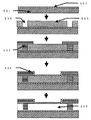
本発明の実施例1における干渉フィルタ製造手段を説明する概略図を図1に示す。ここでは、波長500nmの光を選択透過させる干渉フィルタ例で説明する。透明基板101上に第1反射膜102を蒸着する。次に、犠牲層103をCVDにより250nmの厚さに成膜する。犠牲層103をパターンニングし、アンカー穴104を形成する。パターンニングされた犠牲層103上に、金属膜105を、アンカー穴に沿うように成膜する。ここで、金属膜を用いたが、膜の材質は環境変化に対し劣化しない物であればどのような材質でも良い。また、樹脂をスピンコートなどで塗布し硬化させる方法でも良い。次に、この金属膜をパターンニングし、光の透過する部分を除去する。パターンニングされた金属膜の上面に第2反射膜106を蒸着した後、犠牲層103をエッチングにより除去する事で107に示す、間隔250nmの空気層が得られる。この様な製造手段によると、透明基板101の表面に多少のうねりが存在しても、犠牲層103がそのうねりに沿い堆積していくため、うねりにより間隔の誤差を生じず、場所によらず一様な間隔を持つ干渉フィルタが製造できる。
【0012】
(実施例2)
実施例2における干渉フィルタ製造手段を説明する概略図を図2に示す。ここでも、波長500nmの光を選択透過させる干渉フィルタ例で説明する。透明基板101上に第1反射膜102を蒸着する。次に、犠牲層103をCVDにより250nmの厚さに成膜する。ここで、犠牲層103にアンカー穴104を設ける。金属膜105を、アンカー穴に沿うように成膜を行い、光が透過する部分をエッチングで除去する。次に第2反射膜106を蒸着した後、第2反射膜上に透明樹脂をスピン塗布し、硬化させる。ここで、透明樹脂をスピン塗布する例を示したが、無機のSiO2等の膜を成膜することでも良い。最後に、犠牲層103をエッチングにより除去する事で間隔107が得られる。第2反射膜106上に樹脂膜が有る為、第2反射膜は強固となり、大面積の干渉フィルタが製造可能となる。また、樹脂膜201が保護層としても機能する為、より信頼性の高い干渉フィルタが実現できる。
【0013】
(実施例3)
実施例3における干渉フィルタを説明する概略図を図3に示す。実施例1、及び、2の手段により作成された干渉フィルタは、透明基板301上に第1反射膜302、位相整合条件を満たす空間303を有し、第2反射膜304の上部に透明部材を有し、支柱によって支えられている。303の間隔は波長500nmの光を選択透過させる為、250nmになっている。入射光305は反射膜302と304の間で306に示すように反射、干渉を繰り返し、位相整合条件に合った波長のみ選択透過し、出射光309として得られる。
【0014】
透明基板301の表面にうねりが存在しても、うねりを犠牲層が追従し、その上に着く反射膜304も前記うねりを反映する為、場所による間隔の差は非常に少なくなり、ある場所での間隔307と他の場所での間隔308は等しくなるのである。従って、場所により干渉波長がずれることのない精度の良い干渉フィルタが得られる。ここで得られた干渉フィルタの波長に対する透過率を示したグラフを図4に示す。
【0015】
(実施例4)
実施例4における干渉フィルタ製造手段を説明する概略図を図5に示す。透明基板501上に第1反射膜502を蒸着する。次に、アモルファス・シリコン膜を犠牲層に用い、アモルファス・シリコン膜503をCVDで成膜する。ここで、アモルファス・シリコン犠牲層503にアンカー穴504を設ける。パターンニングされた犠牲層303上に、金属膜505を、アンカー穴に沿うように成膜する。次に、この金属膜をパターンニングし、光の透過する部分を除去する。パターンニングされた金属膜の上面に第2反射膜506を蒸着した後、アモルファス・シリコン犠牲層503を弗化キセノンガスによるエッチングで除去することにより、507に示す空間が確保できる。アモルファス・シリコンは300℃以下で成膜できる為、上下の反射膜に高温で溶融してしまうアルミ合金系の膜を用いることができる。また、弗化キセノンガスによるエッチングは、ドライなプロセスである為、液体プロセスで見られる、吸着現象などが起こらず歩留まりの高い製造工程が得られる。また、プラズマを使ったドライプロセスでもないので、反射膜、及び、透明樹脂等にダメージが無く製造でき、平面性を損なう事の無い製造手段が得られる。
【0016】
(実施例5)
実施例5における干渉フィルタ製造手段を図6により説明する。アモルファス・シリコン犠牲層503にアンカー穴を作成し、反射膜601を成膜する。この時、反射膜がアンカー穴に確実に入り込む成膜を行う。成膜後の形状は、犠牲層のアンカー穴にならう形となる。この上に透明樹脂602をつける時も反射膜の窪みを埋めるように樹脂を充填させる。樹脂硬化後、アモルファス・シリコン犠牲層503を弗化キセノンガスによるエッチングで除去することにより、603に示す間隔が確保できる。
【0017】
この方法により、新たな部材を必要とせず正確な間隔を保つ為の支柱及び、壁が反射膜601と樹脂膜602によって得られる。本実施例では、反射膜、上部の透明樹脂共にアンカー穴に充填させたが、反射膜をアンカー穴部分には成膜せず、透明樹脂のみをアンカー穴に充填しても、同様の支柱、及び、壁が形成できる。
【0018】
(実施例6)
実施例6における干渉フィルタ製造手段を図7により説明する。透明基板501上に第1反射膜502を蒸着する。次に、アモルファス・シリコン膜を犠牲層に用い、アモルファス・シリコン膜503をCVDで成膜する。ここで、アモルファス・シリコン犠牲層503にアンカー穴を設ける。次に第2反射膜601を蒸着した後、そこに、透明接着剤701を塗布し、ガラス板702を接着する。この例ではガラス板を用いたが他の無機材料でも、有機材料でも同じように機能する。ガラス板702を接着後、アモルファス・シリコン犠牲層503を弗化キセノンガスによるエッチング除去することにより、703に示す間隔を確保でき、透過する場所により波長分布の非常に少ない干渉フィルタを製造する手段が得られる。本実施例の製造手段では反射膜601にガラス板が接着されるので、非常に強固な変形を受け難い干渉フィルタが製造できる。
【0019】
(実施例7)
実施例7における干渉フィルタ製造手段を図7により説明する。透明基板501上に第1反射膜502を蒸着する。次に、アモルファス・シリコン膜を犠牲層に用い、アモルファス・シリコン膜503をCVDで成膜する。ここで、アモルファス・シリコン犠牲層503にアンカー穴を設ける。次に第2反射膜601を蒸着した後、そこに、透明接着剤701を塗布し、ガラス板702を接着する。ここで透明接着剤は、硬化後の屈折率がほぼ、ガラス版702の屈折率に等しくされている。この例ではガラス板を用いたが他の無機材料でも、有機材料でも接着される基板の屈折率にほぼ合わせた接着剤を用いれば、本実施例と同じように機能する。ガラス板702を接着後、アモルファス・シリコン犠牲層503を弗化キセノンガスによるエッチング除去することにより、703に示す間隔を持つ干渉フィルタ製造手段が得られる。本実施例により、接着層の境界での反射屈折が非常に少なくなり、光量損失のほとんど無い干渉フィルタが得られる。
【0020】
(実施例8)
実施例8における干渉フィルタを図8により説明する。807の光が透明部材801に入射し、反射膜802に到達する。反射膜802と反射膜805の間には、アモルファス・シリコン犠牲層を弗化キセノンガスによってエッチング除去された空間803が存在する。反射膜802を透過した光は反射膜802,805と間隔803によって干渉を起こし、位相整合条件を満たす波長のみが出射光808となり透過する。
本実施例では、透明部材806の表面に凹凸809が生じていても、反射膜805及び犠牲層、上部反射膜802ともに凹凸809に沿った形で堆積され製作される為、凸部の間隔810と、凹部の間隔811に差が生ずる事無く、どの場所でも、目標の波長を透過させる間隔が保てる。従って、より干渉フィルタの面内で透過波長のばらつきのほとんど無い干渉フィルタが得られる。
【0021】
(実施例9)
実施例9における干渉フィルタを図9により説明する。909の光が透明部材に入射する。この時、透明部材902の光入射側には無反射コート901を設けられている為、透明部材902の入射面での表面反射は極めて少ない。透明ガラス902に入射した光は、接着層903を透過し反射膜904に到達する。反射膜904と反射膜906の間には、アモルファス・シリコン犠牲層を弗化キセノンガスによってエッチング除去された空間905を有する。反射膜904を透過した光は反射膜904,906と間隔905によって910に示すように多重反射時に干渉を起こし、位相整合条件を満たす波長のみが出射光911となり透明基板907を透過する。透明基板907の光出射面には無反射コート911を着けてある。このように、本実施例では、干渉フィルタの入射側、出射側夫々で数%発生していた光量損失をほぼ無くす事ができ、より光利用効率の高い干渉フィルタが得られる。
【0022】
(実施例10)
実施例10における波長可変干渉フィルタを図10により説明する。本実施例の波長可変干渉フィルタは、透明基板1001上に、反射膜1003、及び、下電極1002を有し、支柱1010に支えられたばね構造1008により、上電極1005及び透明部材1009を支える構造を持つ。また、透明部材1009には上電極1005及び反射膜1006を有する。この構造において、上電極1005と下電極1002に電圧を印可すると両電極間に引力が発生し透明部材1009を介して接続されている反射膜1006も1007方向に上下させる事ができる。反射膜1006と1003の間隔1004が変化すると、位相整合条件を満たす波長が変化し、波長可変干渉フィルタが実現できる。
理論式で説明すると、干渉フィルタは、位相整合条件を満たす波長で透過率のピークになる。従って、透過率がピークになる波長をλとすると、
λ=2×L/n
となる。
ここで、n:1,2,3、・・・、L:1004の間隔、である。
上記の間隔Lが変化すれば、位相整合条件を満たす波長が変化する為、透過波長のピークも変化するのである。
【0023】
(実施例11)
実施例11における波長可変干渉フィルタの製造手段を図11により説明する。透明基板1101上に、導電性の反射膜を着け、反射膜を1102に示す形状にパターンニングする。その後、アンカーの土台及び、配線となる導電膜を着けパターンニングし1103に示す形状とする。ここで、反射膜となる1102、配線パターン、又はアンカーの土台となる1103ができあがる。次に、犠牲層1104を着けアンカー穴をパターンニングする。犠牲層の上部に導電性の膜を着け、支柱1105、及び、ばね構造となる1106をパターンニングする。次に導電性の反射膜1107を着ける。これにより反射膜1107とばね部1106、支柱1105が導通する。犠牲層1104をエッチングにより除去し、ばね部及び、反射膜1102,1107の間に空間1108を作る。この製造工程により、反射膜1002,1107を上下電極とし、1106のばね構造を持つ静電アクチュエータが製作できると同時に、反射膜1102,1107は干渉フィルタの反射膜としても機能する。反射膜1102と反射膜1107間に電圧を印可する事により、反射膜膜1102と反射膜1107の間隔を制御でき、透過波長を変化できる波長可変干渉フィルタが作成できる。本実施例によれば、反射膜を電極にする為、静電アクチュエータ駆動の為の新たな電極を必要としない波長可変干渉フィルタの製造手段が実現できる。
【0024】
(実施例12)
実施例12における波長可変干渉フィルタ製造手段を図12により説明する。透明基板1101上に、導電性の膜を着け、導電膜をパターンニングし、その後、アンカーの土台及び、配線となる導電膜を着けパターンニングする。ここで、反射膜、配線パターン、又はアンカーの土台に分離される。次に、犠牲層1104を着けアンカー穴をパターンニングする。犠牲層の上部に導電性の膜を着け、支柱、及び、ばね構造となる1204をパターンニングする。次に導電性の反射膜1107を着ける。これにより反射膜1107とばね部1106、支柱が導通する。第2の反射膜1107上に樹脂1201を塗布し、ばね部1204上にある樹脂をパターン除去し1202部に樹脂が無い状態とする。その後、犠牲層1104をエッチングにより除去し、ばね部1204及び、第1の反射膜と第2の反射膜の間に空間1108を作る。この製造工程により、ばね部1204は樹脂1203に動きを抑制されない為、第1、第2反射膜を上下電極とし、1204のばね構造を持つ静電アクチュエータが製作できると同時に、第1、第2の反射膜は干渉フィルタの反射膜としても機能する。第1、第2反射膜間に電圧を印可する事により、第1、第2反射膜間に引力が発生し、ばね1204を撓ませる。第2反射膜1107は、印可電圧による引力とばね力の釣り合ったところで静止し一定の間隔を保つ。このように、印可電圧を制御することにより、第1、第2反射膜膜の間隔を制御でき、透過波長を変化できる波長可変干渉フィルタが作成できる。
【0025】
(実施例13)
実施例13における波長可変干渉フィルタ製造手段を図13により説明する。透明基板1301上に、導電性の反射膜を着け、導電性の反射膜をパターンニングする事により、アンカーの土台となる1302、反射膜となる1303、配線パターンに分離される。次に、犠牲層1305を着けアンカー1304をパターンニングする。犠牲層の上部に導電性の反射膜1306を着け、反射膜部、配線部、及び、ばね部をパターンニングする。その後、上部に透明部材を塗布し、硬化後、パターンニングすることにより1308部を除去する。この部分は、ばね部の上部に当たる部分である。犠牲層1305を除去する事により、反射膜1309,1310を上下電極とする静電アクチュエータが製作できると同時に、反射膜1309,1310は干渉フィルタの反射膜としても機能する。また、ばね部1311は変位を抑制する樹脂が除去されている為、ばねとして正常に機能できる。従って、反射膜1309と反射膜1310間に電圧を印可する事により、反射膜のばね部1311が撓み、反射膜1309を1312に示すように移動できる。これにより、反射膜1309と反射膜1310の間隔を制御でき、電圧制御により透過波長を変化できる波長可変干渉フィルタが作成できる。また、静電アクチュエータと波長可変干渉フィルタとを同じ導電膜で製作できる為。大幅な製造工程削減ができる。
【0026】
(実施例14)
実施例14における波長可変干渉フィルタ製造手段を図13により説明する。反射膜成膜、パターンニング後アモルファス・シリコン膜を犠牲層としてCVDにより成膜する。アモルファス・シリコンは300℃以下で成膜できる為、アルミ系の膜を用いることができる。その後、アンカー1304をパターンニングする。犠牲層の上部に導電性の膜1306を着け、反射膜部、配線部、及び、ばね部をパターンニングし、上部に透明部材を塗布後、硬化させる。その後、上部に透明部材を塗布し、硬化後、パターンニングすることにより1308部を除去する。この状態で、アモルファス・シリコン犠牲層を弗化キセノンガスにより除去する。弗化キセノンガスで犠牲層除去工程では、液体プロセスでない為、吸着等の不具合も発生しない。しかも、プラズマも使わない為、反射膜にダメージを与えず設計反射率を維持できる。また、アルミ系の反射膜が使える為、ばね常数を小さくでき、それにより、静電アクチュエータ駆動電圧も低くできる。
【0027】
(実施例15)
実施例15における波長可変干渉フィルタ製造手段を図14により説明する。透明基板1401上に、反射膜を成膜後、パターンニングを行い1402に示す形状とする。次に導電性の膜を成膜後、導電膜をパターンニングにより1403部を形成する。1403上に圧電素子1404を接合し、上部に犠牲層1405成膜後、圧電素子1404の上面を露出させるため、アンカー穴1406をパターンニングする。この上に反射膜1406を成膜後、透明樹脂1407を塗布する。本実施例では透明樹脂を用いたが、SiO2に代表される無機材質の膜でも良い。前記透明樹脂硬化後、犠牲層1405をエッチング除去する。これにより、反射膜間に空間1409が生じ、圧電素子に電圧を印可し、圧電素子を伸縮させれば、反射膜1408を上下させる事ができる。従って、反射膜膜1402と反射膜1408の間隔を制御でき、電圧制御により透過波長を変化できる波長可変干渉フィルタが作成できる。
【0028】
(実施例16)
実施例16における波長可変干渉フィルタ製造手段を図15により説明する。透明基板上に反射膜が成膜され、圧電素子1501が接合される。上部にアモルファス・シリコン犠牲層1502成膜後、圧電素子1501の上面を露出させるため、パターンニングによりアンカー穴1503を作成する。この上に反射膜1504を成膜後、接着剤1505を塗布する。接着剤1505は紫外線硬化性を持つ。透明ガラス1506には圧電素子1501の高さと、反射膜に挟まれた光干渉部の厚さの差に合わせた段差1507が設けられており、塗布された接着剤1505を介して、凹凸をかみ合わせるよう接合される。透明ガラス1506接合後、弗化キセノンガスによりアモルファス・シリコン犠牲層1502を除去し、上下の反射膜間に間隔1509を作り出す。本実施例では紫外線硬化タイプの接着剤を用いたが窪みの設けられた透明部材1306の屈折率とほぼ同じ屈折率を有するものであればどのようなタイプの接着剤でも良い。本実施例によれば、圧電アクチュエータを厚することができ、間隔1509の変位量が大きく、駆動電圧も下げる事ができる。
【0029】
従って、本実施例で製造される波長可変干渉フィルタは、低電圧で駆動でき、しかも、反射膜間の間隔変化量を大きく取れる為、紫外光から赤外光までの幅広い範囲で透過波長を変化させる事ができる。
【0030】
(実施例17)
実施例17におけるカラーシーケンシャル用波長選択フィルタを図16により説明する。透明基板1601に反射膜1602、圧電素子1603を有し、圧電素子1603が透明部材1605を支える形で、反射膜1602と反射膜1604との間隔を保持している。この状態で圧電素子1603に電圧を印可すると反射膜1602と反射膜1604の間隔が変化する。反射膜1602と反射膜1604の間隔の変化すると位相整合条件を満たす波長が変化する為、透過波長が変化する。反射膜1602と反射膜1604の間隔は、電圧0Vの時200nm、電圧10Vの時250nm、電圧20Vの時300nmとなる。前記の各電圧に対する透過波長特性を図17に示す。本実施例では電圧0Vの時(青)、電圧10Vの時(緑)、電圧20Vの時(赤)の3原色を表示する。タイミング信号と駆動電圧を示す概略図を図18に示す。プロジェクタ等の画像駆動回路からのタイミング発生回路により、赤のタイミング信号1801が発生され、このタイミングで駆動電圧は1802に示す20Vとなる。この時、反射膜1602と反射膜1604の間隔は300nmとなり、位相整合条件を満たす波長は600nmの赤色となる。また、緑のタイミング信号1803のタイミングで駆動電圧は1804に示す10Vとなり、反射膜1602と反射膜1604の間隔は250nmとなり、位相整合条件を満たす波長は500nmの緑色となる。同様に、青のタイミング信号1805で駆動電圧は1806の0Vとなり、反射膜1602と反射膜1604の間隔は200nmとなり、位相整合条件を満たす波長は400nmの青色となる。
【0031】
この様に本実施例では、時間的シーケンシャルに色を変化させるカラーシーケンシャル用波長選択フィルタが実現できる。また、色の変化する時間は、アクチュエータの動く時間と等しく、非常に光速に色スイッチングが可能となる。しかも、従来のカラーフィルターをモータで回転させるタイプの者と比べ、カラーフィルター上で光束を絞る必要が無い為、光利用効率が高くできる利点も備えている。
【0032】
(実施例18)
実施例18における波長選択フィルタを図19により説明する。光ファイバー1906から出射した光は波長多重されている為、数波長間隔ごとにピークを持つ光が重ね合わされている。この光がレンズ1907により平行または、収束光1908となり透明部材1905に入射する。透明基板1905には、高反射率の反射膜1904を有する。透明部材1905には圧電素子1903を有し、圧電素子1903が透明部材1901を支える形で、反射膜1902と1904との間隔を保持している。この状態で圧電素子1903に電圧を印可すると反射膜1902と反射膜1904の間隔が変化する。反射膜1902と反射膜1604の間隔の変化すると位相整合条件を満たす波長が変化する為、透過波長が変化するので、波長多重された光1908も出射光1909では必要な光のみ分離されるのである。出射光1909は、レンズ1910により光ファイバー1911に挿入される。反射膜1902と反射膜1604は高反射率である為、透過スペクトル分布の半値幅が非常に狭くでき、圧電アクチュエータで反射膜1902と反射膜1604の間隔を非常に精度良く制御できる為、数波長間隔にピークを持つ光も個々のスペクトル波形に分離し透過させることができるのである。
【0033】
【発明の効果】
以上説明したように本発明によれば、
1)位相整合条件を満たす間隔を犠牲層で作成する為、非常に精度の良い間隔が広い範囲で得られる。
2)犠牲層にアンカー穴を設け、それによって間隔を保つ為の支柱、又は、壁を作成し、安定した反射膜間距離を得る事ができる。
3)第2反射膜上に透明部材を塗布する事により、反射膜の保護ができる。
4)お互いの反射膜の間隔を作成時に、低温で成膜できるアモルファス・シリコン犠牲層を用いることにより、高温で損傷の起こるアルミ系の膜が使用可能となり、より吸収の少ない反射率の高い膜が反射膜として実現できた。
5)アモルファス・シリコン犠牲層と、弗化キセノンガスによる犠牲層エッチングプロセスは、ドライなプロセスである為、液体プロセスで見られる、吸着現象などが起こらず歩留まりの高い製造工程が得られる。また、プラズマを使ったドライプロセスでもないので、反射膜、及び、透明樹脂等にダメージが無く製造でき、平面性を損なう事の無い製造手段が得られる。
6)反射膜又は、透明樹脂でアンカー穴を充填させる製造方法により、新たな部材を必要とせず正確な間隔を保つ為の支柱及び、壁が得られる。
7)接着剤の屈折率を透明部材の屈折率に合わせる事により、接着層の境界で反射屈折が非常に少なくなり、光量損失のほとんど無い干渉フィルタが得られる。
8)透明基板の表面に多少のうねりが存在しても、犠牲層がそのうねりに沿い堆積していくため、曲面を持った光学部品上でも、うねりによる間隔の誤差を生ずる事の無い干渉フィルタ製造手段が得られる。
9)透明部材の光入射側と他方の透明部材の出射側に無反射コートを設ける事により、干渉フィルタの入射側、出射側夫々で数%発生していた光量損失をほぼ無くす事ができ、より光利用効率の高い干渉フィルタが得られる。
10)反射膜間の間隔を、静電アクチュエータ、又は、圧電アクチュエータ等を用いて電圧により変化させる事により、透過波長を変化させる事ができる。
11)反射膜を静電アクチュエータの電極を兼ねる構造とすることにより、静電アクチュエータ駆動用の新たな電極を必要としない波長可変干渉フィルタの製造手段が実現できる。
12)反射膜をパターンニングし、配線、電極、支柱を作成している為、製造工程がより短縮された波長可変干渉フィルタの製造手段が実現できる。
13)透明部材に圧電素子の厚みに相当する段差を設け、その段差に圧電素子を接着剤で接合することで、反射膜の間隔に対し、圧電素子の厚みを大きく取れる為、低電圧化が可能となる。また、反射膜の間隔変化量を大きく取れるため、紫外光から赤外光までの可変は長域の広い、波長可変干渉フィルタが実現できる。
14)本発明のカラーシーケンシャル用波長可変フィルタは、非常に高速な色スイッチング速度が得られる。しかも、カラーフィルター上で光束を絞る必要が無い為、光利用効率が高くできる。
14)非常に透過スペクトル幅(透過光波長におけるの半値幅)が非常に小さく、しかも、アクチュエータが非常に精度良く移動できる為、波長選択分解能が高い波長選択フィルタが実現できる。
【図面の簡単な説明】
【図1】 本発明の実施例1における干渉フィルタ製造手段を説明する概略図である。
【図2】 本発明の実施例2における干渉フィルタ製造手段を説明する概略図である。
【図3】 本発明の実施例3における干渉フィルタを説明する概略図である。
【図4】 本発明の実施例3における透過率を示したグラフを示す図である。
【図5】 本発明の実施例4における干渉フィルタ製造手段を説明する概略図である。
【図6】 本発明の実施例5における干渉フィルタ製造手段を説明する概略図である。
【図7】 本発明の実施例6、7における干渉フィルタ製造手段を説明する概略図である。
【図8】 本発明の実施例8における干渉フィルタを示す概略図である。
【図9】 本発明の実施例9における干渉フィルタを示す概略図である。
【図10】 本発明の実施例10における波長可変干渉フィルタを示す概略図である。
【図11】 本発明の実施例11における波長可変干渉フィルタの製造手段を説明する概略図である。
【図12】 本発明の実施例12における波長可変干渉フィルタの製造手段を説明する概略図である。
【図13】 本発明の実施例13、14における波長可変干渉フィルタの製造手段を説明する概略図である。
【図14】 本発明の実施例15における波長可変干渉フィルタの製造手段を説明する概略図である。
【図15】 本発明の実施例16における波長可変干渉フィルタの製造手段を説明する概略図である。
【図16】 本発明の実施例17におけるカラーシーケンシャル用波長選択フィルタを示す図である。
【図17】 本発明の実施例17における各電圧に対する透過波長特性のグラフを示す図である。
【図18】 本発明の実施例17におけるタイミング信号と駆動電圧を示す図である。
【図19】 本発明の実施例18における波長選択フィルタを示す図である。
【符号の説明】
101 透明基板
102、106 反射膜
103 犠牲層
104 アンカー穴
105 金属膜
201 樹脂膜
301 透明基板
302、304 第2反射膜
501 透明基板
502、506 反射膜
503 アモルファス・シリコン膜
504 アンカー穴
505 金属膜
601 反射膜
602 樹脂膜
701 透明接着剤
702 ガラス板
801 透明部材
802、805 反射膜
806 透明部材
901 無反射コート
902 透明部材
903 接着層
904、906 反射膜
907 透明基板
1001 透明基板
1002 下電極
1003、1006 反射膜
1005 上電極
1009 透明部材
1010 支柱
1101 透明基板
1102、1107 反射膜
1104 犠牲層
1105 支柱
1106 ばね部
1201 樹脂
1301 透明基板
1302 アンカー土台
1303、1306、1309、1310 反射膜
1304 アンカー
1305 犠牲層
1311 ばね部
1401 透明基板
1402、1408 反射層
1404 圧電素子
1405 犠牲層
1406 アンカー穴
1407 樹脂層
1501 圧電素子
1502 犠牲層
1503 アンカー穴
1504 反射膜
1505 接着剤
1506 透明ガラス
1601 透明基板
1602、1604 反射膜
1603 圧電素子
1605 透明部材
1901 透明部材
1902、1904 反射膜
1903 圧電素子
1905 透明基板
1906、1911 光ファイバー
1907、1910 レンズ[0001]
BACKGROUND OF THE INVENTION
The present invention relates to a wavelength selective interference filter and optical communication.
[0002]
[Prior art]
Conventionally, interference filters using this type of Fabry-Perot resonator have been widely used from spectroscopes to optical communications because they exhibit wavelength selectivity with a very low half-value width by increasing the reflectivity. . This interference filter multi-reflects between reflection films and transmits only wavelengths that satisfy the phase matching condition (the phase difference of light when reciprocating is an integer multiple of 2π). Conventional configurations have been made by a method in which glass is polished on both sides and a reflective film is deposited on both ends thereof. In addition, as a method of changing the selection wavelength, it is created by a method in which one side of glass is wedge-polished at a slight angle with respect to the other side and a reflecting film is deposited on both ends thereof, and the light incident position is made parallel. Alternatively, a means for changing only the wavelength satisfying the phase matching condition by changing the distance between the reflecting films by rotating is used.
However, this interference filter is expensive because it is necessary to polish the glass very flatly with high surface accuracy and it is very difficult to control the distance.
Further, the wavelength variable interference filter has a problem that it takes time to change the wavelength because it is rotated or translated by a motor or the like.
[0003]
[Problems to be solved by the invention]
The present invention is for solving the above-mentioned problems, is inexpensive, has no deviation in reflection and transmission wavelengths depending on the location, realizes an accurate interference filter, and can switch the selection wavelength at a very high speed. The main object is to realize a wavelength tunable interference filter, and to realize a color sequential wavelength tunable interference filter that is small and can perform selective wavelength switching at high speed.
[0004]
[Means for Solving the Problems]
In order to solve the above-described problem, a first interference filter manufacturing method of the present invention includes:
Forming a first reflective film on a transparent substrate in a first step;
Forming a sacrificial layer film corresponding to a thickness satisfying a phase matching condition for a wavelength to be transmitted or reflected on the first reflective film in the second step;
Forming an anchor hole in the sacrificial layer film in a third step;
Forming a film along the anchor hole on the sacrificial layer film having the anchor hole in a fourth step;
Removing a portion that transmits or reflects light of the film formed in the fourth step by patterning in the fifth step;
Forming a second reflective film on the sacrificial layer and the film patterned in the fifth step in a sixth step;
Forming a resin film by applying and curing a transparent resin on the second reflective film in a seventh step;
Removing the sacrificial layer film in an eighth step;
Characterized by.
In the manufacturing method of the first interference filter,
The sacrificial layer film is made of silicon,
In the eighth step, the sacrificial layer film is removed by a xenon fluoride gas;
Is preferred.
[0005]
The second interference filter manufacturing method of the present invention includes:
Forming a first reflective film on a transparent substrate in a first step;
Forming a sacrificial layer film corresponding to a thickness satisfying a phase matching condition for a wavelength to be transmitted or reflected on the first reflective film in the second step;
Forming an anchor hole in the sacrificial layer film in a third step;
Forming a second reflective film along the anchor hole on the sacrificial layer film having the anchor hole in a fourth step;
In the fifth step, a transparent resin is applied and cured to form a resin film on the second reflective film, and the anchor hole is filled with the resin.
Removing the sacrificial layer film in a sixth step;
It is characterized by.
[0006]
In addition, the third interference filter manufacturing method of the present invention includes:
Forming a first reflective film on the first transparent substrate in the first step;
Forming a sacrificial layer film corresponding to a thickness satisfying a phase matching condition for a wavelength to be transmitted or reflected on the first reflective film in the second step;
Forming an anchor hole in the sacrificial layer film in a third step;
Forming a second reflective film along the anchor hole on the sacrificial layer film having the anchor hole in a fourth step;
Bonding a second transparent substrate on the second reflective film in a fifth step;
Removing the sacrificial layer film in a sixth step;
It is characterized by.
In the third interference filter manufacturing method,
In the fifth step, it is preferable that the refractive index after curing of the adhesive used for bonding the second transparent substrate is substantially equal to the refractive index of the second transparent substrate.
[0007]
The first interference filter of the present invention is an interference filter manufactured by the first to third interference filter manufacturing method,
The first reflective film and the second reflective film have an interval filled with a vacuum or transparent gas equivalent to a thickness that satisfies a phase matching condition with respect to a wavelength to be transmitted or reflected.
A second interference filter according to the present invention is an interference filter manufactured by the third interference filter manufacturing method,
Between the first reflective film and the second reflective film, there is an interval filled with a vacuum or transparent gas equivalent to a thickness that satisfies the phase matching condition for the wavelength to be transmitted or reflected,
A surface of the first transparent substrate on which the first reflective film is not formed or a surface of the second transparent substrate on which the second reflective film is not formed, on which light enters or exits A non-reflective coating is provided.
[0008]
The manufacturing method of the 1st wavelength variable interference filter of this invention is the following.
Forming a first reflective film on a transparent substrate in a first step;
Forming a wiring line at a position where the first reflective film is not formed on the transparent substrate in a second step;
Forming a sacrificial layer on the transparent substrate on which the first reflective film and the wiring lines are formed in a third step;
Forming an anchor hole in the sacrificial layer film in a fourth step;
Forming a film along the anchor hole on the sacrificial layer film having the anchor hole in a fifth step;
In the sixth step, patterning the film formed in the fifth step to create a column and a spring part;
Forming a second reflective film on the sacrificial layer and the film patterned in the fifth step in a seventh step;
Forming a resin film by applying and curing a resin on the second reflective film in an eighth step;
In the ninth step, removing the resin film on the support column and the spring portion;
Removing the sacrificial layer in a tenth step;
A method of manufacturing a wavelength tunable interference filter characterized by the above.
The second tunable interference filter manufacturing method of the present invention is as follows.
Forming a base, a first reflective film, and a first wiring pattern on a transparent substrate in a first step;
Forming a sacrificial layer film on the transparent substrate on which the base, the reflective film, and the wiring pattern are formed in a second step;
Removing the sacrificial layer film on the foundation in a third step to form an anchor hole;
Forming a second reflective film, a second wiring pattern, and a film constituting a spring portion on the sacrificial film having the anchor hole in a fourth step;
In the fifth step, a transparent resin is applied and cured to form a resin film on the second reflective film, the second wiring pattern, and the film constituting the spring portion, and Filling the anchor hole with the resin,
Removing the resin film on the film constituting the spring portion in a sixth step;
Removing the sacrificial layer in a seventh step;
It is characterized by.
[0009]
The third tunable interference filter manufacturing method of the present invention is as follows.
Forming a first reflective film on a transparent substrate in a first step;
In the second step, a conductive film is provided on the first reflective film, leaving an electrode and a wiring pattern, and removing a conductive film present on a light reflecting or transmitting surface;
In a third step, bonding one surface of the piezoelectric element to the electrode;
Forming a sacrificial layer film on the transparent substrate on which the electrode, the wiring pattern, and the piezoelectric element are formed in a fourth step, and removing the sacrificial layer film on the surface of the piezoelectric element;
Forming a second reflective film on the sacrificial layer film and the piezoelectric element in a fifth step;
Providing an organic or inorganic transparent member on the second reflective film in the sixth step;
Removing the sacrificial layer film that has not been removed in the fourth step in the seventh configuration;
It is characterized by.
A fourth method of manufacturing a wavelength tunable interference filter according to the present invention is as follows.
Forming a first reflective film on a transparent substrate in a first step;
In the second step, a conductive film is provided on the first reflective film, leaving an electrode and a wiring pattern, and removing a conductive film present on a light reflecting or transmitting surface;
In a third step, bonding one surface of the piezoelectric element to the electrode;
Forming a sacrificial layer film on the transparent substrate on which the electrode, the wiring pattern, and the piezoelectric element are formed in a fourth step, and removing the sacrificial layer film on the surface of the piezoelectric element;
Forming a second reflective film on the sacrificial layer film and the piezoelectric element in a fifth step;
Adhering an organic or inorganic transparent member on the second reflective film in the sixth step;
Removing the sacrificial layer film that has not been removed in the fourth step in the seventh configuration;
It is characterized by.
In the third and fourth variable wavelength interference filter manufacturing methods,
The sacrificial layer is made of silicon;
In the seventh step, the sacrificial layer film is preferably removed by a xenon fluoride gas.
[0010]
Further, the present invention is a wavelength tunable interference filter manufactured by the first to fourth wavelength tunable interference filter manufacturing method,
The transmission wavelength is changed by changing the distance between the first reflection film and the second reflection film.
It is characterized by that.
[0011]
DETAILED DESCRIPTION OF THE INVENTION
(Example 1)
FIG. 1 is a schematic diagram for explaining an interference filter manufacturing means in
[0012]
(Example 2)
FIG. 2 is a schematic diagram for explaining interference filter manufacturing means in the second embodiment. Here, an example of an interference filter that selectively transmits light having a wavelength of 500 nm will be described. A first
[0013]
(Example 3)
FIG. 3 is a schematic diagram illustrating an interference filter according to the third embodiment. The interference filter created by the means of the first and second embodiments has a first
[0014]
Even if undulation is present on the surface of the transparent substrate 301, the sacrificial layer follows the undulation, and the
[0015]
(Example 4)
FIG. 5 is a schematic diagram for explaining interference filter manufacturing means in the fourth embodiment. A first reflective film 502 is deposited on the
[0016]
(Example 5)
The interference filter manufacturing means in the fifth embodiment will be described with reference to FIG. Anchor holes are created in the amorphous silicon
[0017]
By this method, a support and a wall for maintaining an accurate interval without requiring a new member can be obtained by the reflection film 601 and the
[0018]
(Example 6)
The interference filter manufacturing means in
[0019]
(Example 7)
The interference filter manufacturing means in
[0020]
(Example 8)
An interference filter according to the eighth embodiment will be described with reference to FIG. The light 807 enters the transparent member 801 and reaches the reflective film 802. Between the reflective film 802 and the reflective film 805, there is a space 803 in which the amorphous silicon sacrificial layer is removed by etching with xenon fluoride gas. The light transmitted through the reflective film 802 causes interference due to the reflective films 802 and 805 and the interval 803, and only the wavelength satisfying the phase matching condition is transmitted as the outgoing light 808.
In this embodiment, even if the surface of the transparent member 806 has irregularities 809, the reflective film 805, the sacrificial layer, and the upper reflective film 802 are all deposited and manufactured along the irregularities 809. And the interval which permeate | transmits a target wavelength can be maintained in any place, without producing a difference in the space | interval 811 of a recessed part. Therefore, it is possible to obtain an interference filter with little variation in transmission wavelength in the plane of the interference filter.
[0021]
Example 9
The interference filter according to the ninth embodiment will be described with reference to FIG. Light 909 enters the transparent member. At this time, since the non-reflective coating 901 is provided on the light incident side of the transparent member 902, the surface reflection on the incident surface of the transparent member 902 is extremely small. The light incident on the transparent glass 902 passes through the adhesive layer 903 and reaches the reflective film 904. Between the reflective film 904 and the reflective film 906, there is a space 905 in which the amorphous silicon sacrificial layer is removed by etching with xenon fluoride gas. The light transmitted through the reflection film 904 causes interference at the time of multiple reflection as indicated by 910 by the reflection films 904 and 906 and the interval 905, and only the wavelength satisfying the phase matching condition becomes the output light 911 and passes through the transparent substrate 907. A non-reflective coating 911 is attached to the light exit surface of the transparent substrate 907. As described above, in this embodiment, it is possible to substantially eliminate the light amount loss that occurred at several percent on the incident side and the emission side of the interference filter, and to obtain an interference filter with higher light utilization efficiency.
[0022]
(Example 10)
The variable wavelength interference filter according to the tenth embodiment will be described with reference to FIG. The wavelength tunable interference filter of the present embodiment has a structure in which a reflective film 1003 and a lower electrode 1002 are provided on a transparent substrate 1001, and an upper electrode 1005 and a transparent member 1009 are supported by a spring structure 1008 supported by a
To explain with a theoretical formula, the interference filter has a transmittance peak at a wavelength that satisfies the phase matching condition. Therefore, if the wavelength at which the transmittance reaches a peak is λ,
λ = 2 × L / n
It becomes.
Here, n: 1, 2, 3,..., L: 1004.
If the distance L changes, the wavelength satisfying the phase matching condition changes, and the peak of the transmission wavelength also changes.
[0023]
(Example 11)
A means for manufacturing the wavelength tunable interference filter according to the eleventh embodiment will be described with reference to FIG. A conductive reflective film is applied on the transparent substrate 1101, and the reflective film is patterned into a shape indicated by 1102. Thereafter, the base of the anchor and the conductive film to be the wiring are put on and patterned to obtain the shape shown in 1103. Here, a reflective film 1102, a wiring pattern, or an anchor 1103 is completed. Next, the sacrificial layer 1104 is applied and the anchor holes are patterned. A conductive film is put on the sacrificial layer, and the pillar 1105 and the spring structure 1106 are patterned. Next, a conductive
[0024]
(Example 12)
The wavelength variable interference filter manufacturing means in Embodiment 12 will be described with reference to FIG. A conductive film is applied on the transparent substrate 1101 and a conductive film is patterned, and then a conductive film to be a base of an anchor and a wiring is applied and patterned. Here, it is separated into a reflective film, a wiring pattern, or an anchor base. Next, the sacrificial layer 1104 is applied and the anchor holes are patterned. A conductive film is put on the sacrificial layer, and a pillar and a spring structure 1204 are patterned. Next, a conductive
[0025]
(Example 13)
The wavelength variable interference filter manufacturing means in
[0026]
(Example 14)
The wavelength variable interference filter manufacturing means in
[0027]
(Example 15)
The wavelength variable interference filter manufacturing means in the fifteenth embodiment will be described with reference to FIG. After forming a reflective film on the transparent substrate 1401, patterning is performed to obtain the shape shown in 1402. Next, after forming a conductive film, 1403 parts are formed by patterning the conductive film. A piezoelectric element 1404 is bonded onto 1403, a sacrificial layer 1405 is formed on the top, and then an anchor hole 1406 is patterned to expose the upper surface of the piezoelectric element 1404. A reflective film 1406 is formed thereon, and then a transparent resin 1407 is applied. In this embodiment, a transparent resin is used, but an inorganic material film represented by
[0028]
(Example 16)
The variable wavelength interference filter manufacturing means in the sixteenth embodiment will be described with reference to FIG. A reflective film is formed on the transparent substrate, and the piezoelectric element 1501 is bonded. After the amorphous silicon sacrificial layer 1502 is formed on the upper portion, an anchor hole 1503 is formed by patterning in order to expose the upper surface of the piezoelectric element 1501. An adhesive 1505 is applied after forming a reflective film 1504 thereon. The adhesive 1505 is UV curable. The transparent glass 1506 is provided with a step 1507 according to the difference between the height of the piezoelectric element 1501 and the thickness of the light interference portion sandwiched between the reflection films, and the unevenness is engaged through the applied adhesive 1505. Are joined together. After the transparent glass 1506 is bonded, the amorphous silicon sacrificial layer 1502 is removed with a xenon fluoride gas to create a gap 1509 between the upper and lower reflective films. In this embodiment, an ultraviolet curing type adhesive is used, but any type of adhesive may be used as long as it has a refractive index substantially the same as the refractive index of the transparent member 1306 provided with a depression. According to this embodiment, the thickness of the piezoelectric actuator can be increased, the displacement amount of the interval 1509 is large, and the driving voltage can be lowered.
[0029]
Therefore, the wavelength tunable interference filter manufactured in this embodiment can be driven with a low voltage and can change the transmission wavelength in a wide range from ultraviolet light to infrared light because it can take a large amount of change in the distance between the reflective films. You can make it.
[0030]
(Example 17)
The color sequential wavelength selection filter in Example 17 will be described with reference to FIG. The transparent substrate 1601 has a reflective film 1602 and a piezoelectric element 1603, and the piezoelectric element 1603 supports the transparent member 1605, and the distance between the reflective film 1602 and the reflective film 1604 is maintained. When a voltage is applied to the piezoelectric element 1603 in this state, the distance between the reflective film 1602 and the reflective film 1604 changes. When the distance between the reflective film 1602 and the reflective film 1604 is changed, the wavelength satisfying the phase matching condition is changed, so that the transmission wavelength is changed. The distance between the reflective film 1602 and the reflective film 1604 is 200 nm when the voltage is 0 V, 250 nm when the voltage is 10 V, and 300 nm when the voltage is 20 V. FIG. 17 shows the transmission wavelength characteristics for each voltage. In this embodiment, three primary colors are displayed when the voltage is 0V (blue), when the voltage is 10V (green), and when the voltage is 20V (red). A schematic diagram showing timing signals and drive voltages is shown in FIG. A red timing signal 1801 is generated by a timing generation circuit from an image driving circuit such as a projector. At this timing, the driving voltage becomes 20 V indicated by 1802. At this time, the distance between the reflective film 1602 and the reflective film 1604 is 300 nm, and the wavelength that satisfies the phase matching condition is 600 nm in red. Further, at the timing of the green timing signal 1803, the drive voltage becomes 10V shown by 1804, the interval between the reflective film 1602 and the reflective film 1604 becomes 250 nm, and the wavelength satisfying the phase matching condition becomes 500 nm green. Similarly, in the blue timing signal 1805, the driving voltage is 1806 of 1806, the distance between the reflective film 1602 and the reflective film 1604 is 200 nm, and the wavelength satisfying the phase matching condition is blue of 400 nm.
[0031]
As described above, in this embodiment, it is possible to realize a color sequential wavelength selection filter that changes colors in a temporally sequential manner. The color change time is equal to the actuator movement time, and color switching can be performed at a very high speed of light. In addition, as compared with a conventional type in which a color filter is rotated by a motor, it is not necessary to focus the light beam on the color filter, so that the light use efficiency can be increased.
[0032]
(Example 18)
The wavelength selection filter in Example 18 will be described with reference to FIG. Since the light emitted from the optical fiber 1906 is wavelength-multiplexed, light having a peak is overlapped every several wavelength intervals. This light becomes parallel or converged light 1908 by the lens 1907 and enters the transparent member 1905. The transparent substrate 1905 has a reflective film 1904 with high reflectivity. The transparent member 1905 includes a piezoelectric element 1903, and the piezoelectric element 1903 supports the transparent member 1901 so that the distance between the reflective films 1902 and 1904 is maintained. When a voltage is applied to the piezoelectric element 1903 in this state, the distance between the reflective film 1902 and the reflective film 1904 changes. When the distance between the reflective film 1902 and the reflective film 1604 is changed, the wavelength satisfying the phase matching condition is changed, and thus the transmission wavelength is changed. Therefore, the wavelength-multiplexed light 1908 is also separated from the output light 1909 only by the necessary light. . The outgoing light 1909 is inserted into the optical fiber 1911 by the lens 1910. Since the reflection film 1902 and the reflection film 1604 have high reflectivity, the half width of the transmission spectrum distribution can be very narrow, and the distance between the reflection film 1902 and the reflection film 1604 can be controlled with high accuracy by a piezoelectric actuator. Light having a peak in the interval can also be separated into individual spectral waveforms and transmitted.
[0033]
【The invention's effect】
As described above, according to the present invention,
1) Since the interval satisfying the phase matching condition is formed by the sacrificial layer, a very accurate interval can be obtained in a wide range.
2) An anchor hole is provided in the sacrificial layer, and thereby a support or wall for maintaining a space is created, and a stable distance between the reflective films can be obtained.
3) The reflective film can be protected by applying a transparent member on the second reflective film.
4) By using an amorphous silicon sacrificial layer that can be deposited at a low temperature when creating the distance between the reflective films, an aluminum-based film that can be damaged at a high temperature can be used. Was realized as a reflective film.
5) Since the sacrificial layer etching process using the amorphous silicon sacrificial layer and the xenon fluoride gas is a dry process, an adsorption phenomenon or the like, which is seen in a liquid process, does not occur and a manufacturing process with a high yield can be obtained. Further, since it is not a dry process using plasma, the reflecting film, the transparent resin, and the like can be manufactured without damage, and a manufacturing means that does not impair the flatness can be obtained.
6) By the manufacturing method in which the anchor hole is filled with a reflective film or transparent resin, a support and a wall for maintaining an accurate interval without requiring a new member can be obtained.
7) By adjusting the refractive index of the adhesive to the refractive index of the transparent member, the reflection refraction at the boundary of the adhesive layer becomes very small, and an interference filter with almost no light loss is obtained.
8) Even if there is some waviness on the surface of the transparent substrate, the sacrificial layer accumulates along the waviness, so that interference filters that do not cause a gap error due to waviness even on optical components with curved surfaces. Manufacturing means are obtained.
9) By providing a non-reflective coating on the light incident side of the transparent member and the output side of the other transparent member, it is possible to almost eliminate the light quantity loss that occurred at several percent on the incident side and the output side of the interference filter, An interference filter with higher light utilization efficiency can be obtained.
10) The transmission wavelength can be changed by changing the interval between the reflective films by a voltage using an electrostatic actuator or a piezoelectric actuator.
11) By making the reflecting film also serve as the electrode of the electrostatic actuator, a means for manufacturing a wavelength variable interference filter that does not require a new electrode for driving the electrostatic actuator can be realized.
12) Since the reflective film is patterned and wirings, electrodes, and pillars are created, a means for manufacturing a wavelength tunable interference filter with a shorter manufacturing process can be realized.
13) Since a step corresponding to the thickness of the piezoelectric element is provided in the transparent member, and the piezoelectric element is bonded to the step with an adhesive, the thickness of the piezoelectric element can be increased with respect to the distance between the reflective films. It becomes possible. In addition, since the amount of change in the interval between the reflection films can be increased, a variable wavelength interference filter having a wide long range can be realized from ultraviolet light to infrared light.
14) The color-sequential wavelength tunable filter of the present invention can obtain a very high color switching speed. In addition, since it is not necessary to focus the light beam on the color filter, the light utilization efficiency can be increased.
14) Since the transmission spectrum width (half-value width at the transmitted light wavelength) is very small and the actuator can be moved with high accuracy, a wavelength selective filter with high wavelength selection resolution can be realized.
[Brief description of the drawings]
FIG. 1 is a schematic diagram for explaining interference filter manufacturing means in
FIG. 2 is a schematic diagram for explaining interference filter manufacturing means in
FIG. 3 is a schematic diagram illustrating an interference filter according to a third embodiment of the present invention.
FIG. 4 is a graph showing the transmittance in Example 3 of the present invention.
FIG. 5 is a schematic diagram for explaining interference filter manufacturing means in
FIG. 6 is a schematic diagram for explaining interference filter manufacturing means in
FIG. 7 is a schematic diagram for explaining interference filter manufacturing means in
FIG. 8 is a schematic diagram illustrating an interference filter according to an eighth embodiment of the present invention.
FIG. 9 is a schematic diagram illustrating an interference filter according to a ninth embodiment of the present invention.
FIG. 10 is a schematic diagram showing a variable wavelength interference filter according to a tenth embodiment of the present invention.
FIG. 11 is a schematic diagram for explaining a means for manufacturing a wavelength variable interference filter according to an eleventh embodiment of the present invention.
FIG. 12 is a schematic diagram for explaining means for manufacturing a wavelength variable interference filter according to a twelfth embodiment of the present invention.
FIG. 13 is a schematic view for explaining means for manufacturing a wavelength tunable interference filter according to Examples 13 and 14 of the present invention.
FIG. 14 is a schematic diagram for explaining a means for manufacturing a wavelength variable interference filter according to a fifteenth embodiment of the present invention.
FIG. 15 is a schematic diagram for explaining means for manufacturing a wavelength tunable interference filter according to a sixteenth embodiment of the present invention.
FIG. 16 is a diagram showing a wavelength-sequential wavelength selection filter in Embodiment 17 of the present invention.
FIG. 17 is a graph showing transmission wavelength characteristics with respect to voltages in Example 17 of the present invention.
FIG. 18 is a diagram showing timing signals and drive voltages in Example 17 of the present invention.
FIG. 19 is a diagram illustrating a wavelength selection filter according to an eighteenth embodiment of the present invention.
[Explanation of symbols]
101 Transparent substrate
102, 106 Reflective film
103 Sacrificial layer
104 Anchor hole
105 Metal film
201 resin film
301 Transparent substrate
302, 304 Second reflective film
501 Transparent substrate
502, 506 Reflective film
503 Amorphous silicon film
504 Anchor hole
505 Metal film
601 reflective film
602 Resin film
701 Transparent adhesive
702 glass plate
801 Transparent member
802, 805 reflective film
806 Transparent member
901 Non-reflective coating
902 Transparent member
903 Adhesive layer
904, 906 Reflective film
907 transparent substrate
1001 Transparent substrate
1002 Lower electrode
1003, 1006 Reflective film
1005 Upper electrode
1009 Transparent member
1010 prop
1101 Transparent substrate
1102, 1107 Reflective film
1104 Sacrificial layer
1105 Prop
1106 Spring part
1201 resin
1301 Transparent substrate
1302 Anchor base
1303, 1306, 1309, 1310 Reflective film
1304 Anchor
1305 Sacrificial layer
1311 Spring part
1401 Transparent substrate
1402, 1408 Reflective layer
1404 Piezoelectric element
1405 Sacrificial layer
1406 Anchor hole
1407 Resin layer
1501 Piezoelectric element
1502 Sacrificial layer
1503 Anchor hole
1504 reflective film
1505 Adhesive
1506 transparent glass
1601 Transparent substrate
1602, 1604 Reflective film
1603 Piezoelectric element
1605 Transparent member
1901 Transparent member
1902, 1904 Reflective film
1903 Piezoelectric element
1905 Transparent substrate
1906, 1911 Optical fiber
1907, 1910 Lens
Claims (13)
第2の工程で、前記第1の反射膜上に、透過または反射させる波長に対し、位相整合条件を満たす厚さ相当の犠牲層膜を形成すること、
第3の工程で、前記犠牲層膜にアンカー穴を形成すること、
第4の工程で、前記アンカー穴を持つ前記犠牲層膜上に膜をアンカー穴に沿って形成すること、
第5の工程で、前記第4の工程で形成した膜の、光を透過又は反射させる部分をパターンニングによって除去すること、
第6の工程で、前記犠牲層及び前記第5の工程でパターニングされた前記膜上に、第2の反射膜を形成すること、
第7の工程で、前記第2の反射膜上に透明樹脂を塗布し、硬化させることにより、樹脂膜を形成すること、
第8の工程で、前記犠牲層膜を除去すること、
を特徴とする干渉フィルタの製造方法。 Forming a first reflective film on a transparent substrate in a first step;
Forming a sacrificial layer film corresponding to a thickness satisfying a phase matching condition for a wavelength to be transmitted or reflected on the first reflective film in the second step;
Forming an anchor hole in the sacrificial layer film in a third step;
In the fourth step, the film to be formed along the anchor hole on the sacrificial layer film having the anchor hole,
Removing a portion that transmits or reflects light of the film formed in the fourth step by patterning in the fifth step;
Forming a second reflective film on the sacrificial layer and the film patterned in the fifth step in a sixth step;
Forming a resin film by applying and curing a transparent resin on the second reflective film in a seventh step;
Removing the sacrificial layer film in an eighth step ;
Method for producing an interference filter according to claim.
前記犠牲層膜はシリコンからなり、
前記第8の工程において、前記犠牲層膜は弗化キセノンガスにより除去されること、
を特徴とする干渉フィルタの製造方法。 In the manufacturing method of the interference filter according to claim 1,
The sacrificial layer film is made of silicon,
In the eighth step, the sacrificial layer film is removed by a xenon fluoride gas ;
Method for producing an interference filter according to claim.
第2の工程で、前記第1の反射膜上に、透過又は反射させる波長に対し、位相整合条件を満たす厚さ相当の犠牲層膜を形成すること、
第3の工程で、前記犠牲層膜にアンカー穴を形成すること、
第4の工程で、前記アンカー穴を持つ前記犠牲層膜上に、第2の反射膜をアンカー穴に沿って形成すること、
第5の工程で、透明樹脂を塗布し、硬化させることにより、前記第2の反射膜上に樹脂膜を形成するとともに、前記アンカー穴に前記樹脂を充填すること、
第6の工程で、前記犠牲層膜を除去すること、
を特徴とする干渉フィルタの製造方法。 In the first step, the first reflective film is formed on the transparent substrate.FormationTo do,
In the second step,On the first reflective film,Thickness equivalent to the phase matching condition for the wavelength to be transmitted or reflectedSacrificial layer film is formedTo do,
In the third step,Sacrificial layer filmForming an anchor hole in the
In the fourth step, having the anchor holeSaidSacrificial layerfilmabove,A second reflective film along the anchor holeFormationTo do,
In the fifth step,A transparent resin is applied and cured to form a resin film on the second reflective film, andAnchor holeThe resinFilling,
In the sixth step,Remove the sacrificial layer filmTo do,
TheA method for manufacturing an interference filter.
第2の工程で、前記第1の反射膜上に、透過又は反射させる波長に対し、位相整合条件を満たす厚さ相当の犠牲層膜を形成すること、
第3の工程で、前記犠牲層膜にアンカー穴を形成すること、
第4の工程で、前記アンカー穴を持つ犠牲層膜上に第2の反射膜をアンカー穴に沿って形成すること、
第5の工程で、前記第2の反射膜上に、第2の透明基板を接着すること、
第6の工程で、前記犠牲層膜を除去すること、
を特徴とする干渉フィルタの製造方法。 Forming a first reflective film on the first transparent substrate in the first step;
Forming a sacrificial layer film corresponding to a thickness satisfying a phase matching condition for a wavelength to be transmitted or reflected on the first reflective film in the second step;
Forming an anchor hole in the sacrificial layer film in a third step;
Forming a second reflective film along the anchor hole on the sacrificial layer film having the anchor hole in a fourth step;
Bonding a second transparent substrate on the second reflective film in a fifth step;
Removing the sacrificial layer film in a sixth step ;
Method for producing an interference filter according to claim.
前記第5の工程で、前記第2の透明基板を接着するために用いる接着剤の硬化後の屈折率を、前記第2の透明基板の屈折率にほぼ等しくすることを特徴とする干渉フィルタの製造方法。In the manufacturing method of the interference filter according to claim 4 ,
In the fifth step, the refractive index after curing of the adhesive used for bonding the second transparent substrate is made substantially equal to the refractive index of the second transparent substrate . Production method.
前記第1の反射膜と前記第2の反射膜の間に、透過又は反射させる波長に対し位相整合条件を満たす厚さ相当の真空又は透明気体で満たされた間隔を有することを特徴とする干渉フィルタ。An interference filter manufactured by the method for manufacturing an interference filter according to any one of claims 1 to 5 ,
The interference having a space filled with a vacuum or a transparent gas corresponding to a thickness satisfying a phase matching condition with respect to a wavelength to be transmitted or reflected between the first reflective film and the second reflective film filter.
前記第1の反射膜と前記第2の反射膜の間に、透過又は反射させる波長に対し位相整合条件を満たす厚さ相当の真空又は透明気体で満たされた間隔を有し、
前記第1の透明基板の前記第1反射膜が形成されていない面または前記第2の透明基板の前記第2の反射膜が形成されていない面であって、光が入射または出射する面に、無反射コートを設けたことを特徴とする干渉フィルタ。A interference filter manufactured by the manufacturing method of the interference filter according to claim 4 or claim 5,
Between the first reflective film and the second reflective film, there is an interval filled with a vacuum or transparent gas equivalent to a thickness that satisfies a phase matching condition with respect to a wavelength to be transmitted or reflected ,
A surface of the first transparent substrate on which the first reflective film is not formed or a surface of the second transparent substrate on which the second reflective film is not formed, on which light enters or exits An interference filter provided with a non-reflective coating.
第2の工程で、前記透明基板上の、前記第1の反射膜が形成されていない位置に、配線ラインを形成すること、
第3の工程で、前記第1の反射膜及び前記配線ラインが形成された前記透明基板上に、犠牲層を成膜すること、
第4の工程で、前記犠牲層膜にアンカー穴を形成すること、
第5の工程で、前記アンカー穴を持つ犠牲層膜上に膜をアンカー穴に沿って形成すること、
第6の工程で、前記第5の工程で形成した膜をパターンニングし、支柱及びばね部を作成すること、
第7の工程で、前記犠牲層及び前記第5の工程でパターニングされた前記膜上に、第2の反射膜を形成すること、
第8の工程で、前記第2の反射膜上に樹脂を塗布し、硬化させることにより、樹脂膜を形成すること、
第9の工程で、前記支柱及びばね部上に有る前記樹脂膜を除去すること、
第10の工程で、前記犠牲層を除去すること、
を特徴とする波長可変干渉フィルタの製造方法。 Forming a first reflective film on a transparent substrate in a first step;
Forming a wiring line at a position where the first reflective film is not formed on the transparent substrate in a second step;
Forming a sacrificial layer on the transparent substrate on which the first reflective film and the wiring lines are formed in a third step;
Forming an anchor hole in the sacrificial layer film in a fourth step;
Forming a film along the anchor hole on the sacrificial layer film having the anchor hole in a fifth step;
In the sixth step, patterning the film formed in the fifth step to create a column and a spring part;
Forming a second reflective film on the sacrificial layer and the film patterned in the fifth step in a seventh step;
Forming a resin film by applying and curing a resin on the second reflective film in an eighth step;
In the ninth step, removing the resin film present on the strut and spring unit,
Removing the sacrificial layer in a tenth step;
A method of manufacturing a wavelength tunable interference filter characterized by the above.
第2の工程で、前記土台、前記反射膜、及び前記配線パターンが形成された前記透明基板上に、犠牲層膜を形成すること、 Forming a sacrificial layer film on the transparent substrate on which the base, the reflective film, and the wiring pattern are formed in a second step;
第3の工程で、前記土台上の前記犠牲層膜を除去してアンカー穴を形成すること、 Removing the sacrificial layer film on the foundation in a third step to form an anchor hole;
第4の工程で、前記アンカー穴を持つ前記犠牲膜上に、第2の反射膜と、第2の配線パターンと、ばね部を構成する膜と、を形成すること、 Forming a second reflective film, a second wiring pattern, and a film constituting a spring portion on the sacrificial film having the anchor hole in a fourth step;
第5の工程で、透明樹脂を塗布し、硬化させることにより、前記第2の反射膜、前記第2の配線パターン、及び前記ばね部を構成する膜上に、樹脂膜を形成するとともに、前記アンカー穴に前記樹脂を充填すること、 In the fifth step, a transparent resin is applied and cured to form a resin film on the second reflective film, the second wiring pattern, and the film constituting the spring portion, and Filling the anchor hole with the resin,
第6の工程で、前記ばね部を構成する膜上に有る前記樹脂膜を除去すること、 Removing the resin film on the film constituting the spring portion in a sixth step;
第7の工程で、前記犠牲層を除去すること、 Removing the sacrificial layer in a seventh step;
を特徴とする波長可変干渉フィルタの製造方法。A method of manufacturing a wavelength tunable interference filter characterized by
第2の工程で、前記第1の反射膜上に、導電性の膜を設け、電極及び配線パターンを残し、光の反射又は透過する面に存在する導電膜を除去すること、
第3の工程で、前記電極に圧電素子の一方の面を接合すること、
第4の工程で、前記電極、配線パターン、及び前記圧電素子が形成された前記透明基板上に犠牲層膜を形成し、前記圧電素子の面上に有る前記犠牲層膜を除去すること、
第5の工程で、前記犠牲層膜及び前記圧電素子上に、第2の反射膜を成膜すること、
第6の工程で、前記第2の反射膜上に、透明樹脂を塗布し、硬化させることにより、樹脂膜を形成すること、
第7の構成で、前記第4の工程で除去されていない前記犠牲層膜を除去すること、
を特徴とする波長可変干渉フィルタの製造方法。 Forming a first reflective film on a transparent substrate in a first step;
In the second step, a conductive film is provided on the first reflective film, leaving an electrode and a wiring pattern, and removing a conductive film present on a light reflecting or transmitting surface;
Bonding one surface of the piezoelectric element to the electrode in a third step;
In the fourth step, the electrode, the wiring pattern, and a sacrificial layer film is formed on the piezoelectric element is formed the transparent substrate, removing the sacrificial layer film present on the surface of the piezoelectric element that,
Forming a second reflective film on the sacrificial layer film and the piezoelectric element in a fifth step;
Forming a resin film by applying and curing a transparent resin on the second reflective film in a sixth step;
Removing the sacrificial layer film that has not been removed in the fourth step in the seventh configuration;
A method of manufacturing a wavelength tunable interference filter characterized by the above.
第2の工程で、前記第1の反射膜上に、導電性の膜を設け、電極及び配線パターンを残し、光の反射又は透過する面に存在する導電膜を除去すること、
第3の工程で、前記電極に圧電素子の一方の面を接合すること、
第4の工程で、前記電極、配線パターン、及び前記圧電素子が形成された前記透明基板 上に犠牲層膜を形成し、前記圧電素子の面上に有る前記犠牲層膜を除去すること、
第5の工程で、前記犠牲層膜及び前記圧電素子上に、第2の反射膜を成膜すること、
第6の工程で、前記第2の反射膜上に、有機又は無機の透明部材を接着すること、
第7の構成で、前記第4の工程で除去されていない前記犠牲層膜を除去すること、
を特徴とする波長可変干渉フィルタの製造方法。 Forming a first reflective film on a transparent substrate in a first step ;
In the second step, a conductive film is provided on the first reflective film, leaving an electrode and a wiring pattern, and removing a conductive film present on a light reflecting or transmitting surface;
Bonding one surface of the piezoelectric element to the electrode in a third step;
In the fourth step, the electrode, the wiring pattern, and a sacrificial layer film is formed on the piezoelectric element is formed the transparent substrate, removing the sacrificial layer film present on the surface of the piezoelectric element that,
Forming a second reflective film on the sacrificial layer film and the piezoelectric element in a fifth step;
In the sixth step, on the second reflection film, adhering the transparent member of an organic or inorganic,
Removing the sacrificial layer film that has not been removed in the fourth step in the seventh configuration;
A method of manufacturing a wavelength tunable interference filter characterized by the above.
前記犠牲層はシリコンからなり、
前記第7の工程において、前記犠牲層膜は弗化キセノンガスによって除去されること、
を特徴とする波長可変干渉フィルタの製造方法。In the manufacturing method of the wavelength tunable interference filter according to claim 10 or 11 ,
The sacrificial layer is made of silicon,
In the seventh step, the sacrificial layer film is removed by a xenon fluoride gas ;
A method of manufacturing a wavelength tunable interference filter characterized by the above.
前記第1の反射膜と前記第2の反射膜の間の間隔を変化させることにより、透過波長を変化させる The transmission wavelength is changed by changing the distance between the first reflection film and the second reflection film.
ことを特徴とする波長可変干渉フィルタ。A tunable interference filter characterized by the above.
Priority Applications (1)
| Application Number | Priority Date | Filing Date | Title |
|---|---|---|---|
| JP2001037511A JP3858606B2 (en) | 2001-02-14 | 2001-02-14 | Method for manufacturing interference filter, interference filter, method for manufacturing variable wavelength interference filter, and variable wavelength interference filter |
Applications Claiming Priority (1)
| Application Number | Priority Date | Filing Date | Title |
|---|---|---|---|
| JP2001037511A JP3858606B2 (en) | 2001-02-14 | 2001-02-14 | Method for manufacturing interference filter, interference filter, method for manufacturing variable wavelength interference filter, and variable wavelength interference filter |
Publications (3)
| Publication Number | Publication Date |
|---|---|
| JP2002243937A JP2002243937A (en) | 2002-08-28 |
| JP2002243937A5 JP2002243937A5 (en) | 2005-01-27 |
| JP3858606B2 true JP3858606B2 (en) | 2006-12-20 |
Family
ID=18900627
Family Applications (1)
| Application Number | Title | Priority Date | Filing Date |
|---|---|---|---|
| JP2001037511A Expired - Fee Related JP3858606B2 (en) | 2001-02-14 | 2001-02-14 | Method for manufacturing interference filter, interference filter, method for manufacturing variable wavelength interference filter, and variable wavelength interference filter |
Country Status (1)
| Country | Link |
|---|---|
| JP (1) | JP3858606B2 (en) |
Cited By (1)
| Publication number | Priority date | Publication date | Assignee | Title |
|---|---|---|---|---|
| CN110954981A (en) * | 2018-09-27 | 2020-04-03 | 精工爱普生株式会社 | Optical device and electronic apparatus |
Families Citing this family (33)
| Publication number | Priority date | Publication date | Assignee | Title |
|---|---|---|---|---|
| US7297471B1 (en) | 2003-04-15 | 2007-11-20 | Idc, Llc | Method for manufacturing an array of interferometric modulators |
| TW557395B (en) * | 2003-01-29 | 2003-10-11 | Yen Sun Technology Corp | Optical interference type reflection panel and the manufacturing method thereof |
| TW570896B (en) | 2003-05-26 | 2004-01-11 | Prime View Int Co Ltd | A method for fabricating an interference display cell |
| JP3812550B2 (en) | 2003-07-07 | 2006-08-23 | セイコーエプソン株式会社 | Tunable optical filter |
| JP2005045976A (en) * | 2003-07-25 | 2005-02-17 | Matsushita Electric Works Ltd | Electrostatic actuator |
| JP3770326B2 (en) | 2003-10-01 | 2006-04-26 | セイコーエプソン株式会社 | Analysis equipment |
| JP2005165067A (en) | 2003-12-03 | 2005-06-23 | Seiko Epson Corp | Tunable optical filter and method of manufacturing tunable optical filter |
| JP4634057B2 (en) * | 2004-03-17 | 2011-02-16 | アンリツ株式会社 | Optical cavity |
| JP4296974B2 (en) * | 2004-03-24 | 2009-07-15 | 株式会社村田製作所 | Fabry-Perot tunable filter and multi-channel Fabry-Perot tunable filter |
| US7087134B2 (en) * | 2004-03-31 | 2006-08-08 | Hewlett-Packard Development Company, L.P. | System and method for direct-bonding of substrates |
| JP4210245B2 (en) | 2004-07-09 | 2009-01-14 | セイコーエプソン株式会社 | Wavelength tunable filter and detection device |
| KR101354520B1 (en) | 2004-07-29 | 2014-01-21 | 퀄컴 엠이엠에스 테크놀로지스, 인크. | System and method for micro-electromechanical operating of an interferometric modulator |
| US20060066932A1 (en) * | 2004-09-27 | 2006-03-30 | Clarence Chui | Method of selective etching using etch stop layer |
| CN100410723C (en) * | 2005-01-28 | 2008-08-13 | 精工爱普生株式会社 | Optical tunable filter and method for manufacturing the same |
| EP2495212A3 (en) | 2005-07-22 | 2012-10-31 | QUALCOMM MEMS Technologies, Inc. | Mems devices having support structures and methods of fabricating the same |
| KR101375337B1 (en) * | 2005-07-22 | 2014-03-18 | 퀄컴 엠이엠에스 테크놀로지스, 인크. | Electomechanical devices having support structures and methods of fabricating the same |
| US7795061B2 (en) | 2005-12-29 | 2010-09-14 | Qualcomm Mems Technologies, Inc. | Method of creating MEMS device cavities by a non-etching process |
| US7382515B2 (en) | 2006-01-18 | 2008-06-03 | Qualcomm Mems Technologies, Inc. | Silicon-rich silicon nitrides as etch stops in MEMS manufacture |
| US7763546B2 (en) | 2006-08-02 | 2010-07-27 | Qualcomm Mems Technologies, Inc. | Methods for reducing surface charges during the manufacture of microelectromechanical systems devices |
| US7733552B2 (en) | 2007-03-21 | 2010-06-08 | Qualcomm Mems Technologies, Inc | MEMS cavity-coating layers and methods |
| US7719752B2 (en) | 2007-05-11 | 2010-05-18 | Qualcomm Mems Technologies, Inc. | MEMS structures, methods of fabricating MEMS components on separate substrates and assembly of same |
| US7864403B2 (en) | 2009-03-27 | 2011-01-04 | Qualcomm Mems Technologies, Inc. | Post-release adjustment of interferometric modulator reflectivity |
| US8547626B2 (en) | 2010-03-25 | 2013-10-01 | Qualcomm Mems Technologies, Inc. | Mechanical layer and methods of shaping the same |
| JP5625614B2 (en) | 2010-08-20 | 2014-11-19 | セイコーエプソン株式会社 | Optical filter, optical filter module, spectrophotometer and optical instrument |
| JP5577983B2 (en) * | 2010-09-21 | 2014-08-27 | 株式会社デンソー | Manufacturing method of Fabry-Perot interferometer |
| US9134527B2 (en) | 2011-04-04 | 2015-09-15 | Qualcomm Mems Technologies, Inc. | Pixel via and methods of forming the same |
| US8963159B2 (en) | 2011-04-04 | 2015-02-24 | Qualcomm Mems Technologies, Inc. | Pixel via and methods of forming the same |
| US8659816B2 (en) | 2011-04-25 | 2014-02-25 | Qualcomm Mems Technologies, Inc. | Mechanical layer and methods of making the same |
| JP5906640B2 (en) * | 2011-09-29 | 2016-04-20 | セイコーエプソン株式会社 | Wavelength variable interference filter, optical filter device, optical module, and electronic apparatus |
| JP6035768B2 (en) | 2012-02-16 | 2016-11-30 | セイコーエプソン株式会社 | Interference filters, optical modules, and electronics |
| FI125612B (en) * | 2012-05-08 | 2015-12-15 | Teknologian Tutkimuskeskus Vtt Oy | Fabry-Perot interferometer |
| US9638913B2 (en) * | 2013-11-26 | 2017-05-02 | Inphenix, Inc. | Wavelength tunable MEMS-Fabry Perot filter |
| JP7238385B2 (en) * | 2018-12-20 | 2023-03-14 | セイコーエプソン株式会社 | Spectral filter modules, spectroscopic cameras and electronics |
-
2001
- 2001-02-14 JP JP2001037511A patent/JP3858606B2/en not_active Expired - Fee Related
Cited By (1)
| Publication number | Priority date | Publication date | Assignee | Title |
|---|---|---|---|---|
| CN110954981A (en) * | 2018-09-27 | 2020-04-03 | 精工爱普生株式会社 | Optical device and electronic apparatus |
Also Published As
| Publication number | Publication date |
|---|---|
| JP2002243937A (en) | 2002-08-28 |
Similar Documents
| Publication | Publication Date | Title |
|---|---|---|
| JP3858606B2 (en) | Method for manufacturing interference filter, interference filter, method for manufacturing variable wavelength interference filter, and variable wavelength interference filter | |
| US10288870B2 (en) | Wavelength tunable MEMS-Fabry Perot filter | |
| KR101293601B1 (en) | Photonic mems and structures | |
| US5943155A (en) | Mars optical modulators | |
| JP4032216B2 (en) | OPTICAL MULTILAYER STRUCTURE, ITS MANUFACTURING METHOD, OPTICAL SWITCHING DEVICE, AND IMAGE DISPLAY DEVICE | |
| US7447891B2 (en) | Light modulator with concentric control-electrode structure | |
| KR100723549B1 (en) | Fabrication of a reflective spatial light modulator | |
| KR100853131B1 (en) | Method and apparatus for driving electronic device | |
| TWI435372B (en) | Mems device having support structures configured to minimize stress-related deformation and methods for fabricating same | |
| US20040209195A1 (en) | Method for fabricating an interference display unit | |
| JP5640549B2 (en) | Optical filter, optical filter manufacturing method, and optical device | |
| US20070064295A1 (en) | Light modulator with tunable optical state | |
| KR20040111336A (en) | Architecture of a reflective spatial light modulator | |
| US9244266B2 (en) | Tunable optical filter and method of manufacture thereof | |
| JP2002221678A (en) | Optical switching device, method of manufacturing for the same and image display device | |
| WO2003055788A1 (en) | Electrostatic drive mems element, manufacturing method thereof, optical mems element, optical modulation element, glv device, and laser display | |
| KR20040111335A (en) | Reflective spatial light modulator | |
| JP4404174B2 (en) | Optical switching element, switching device using the same, and image display device | |
| JP4830183B2 (en) | Optical multilayer structure, optical switching element, and image display device | |
| CN104698584B (en) | Double-beam type thermally-driven tunable filter and manufacturing method thereof | |
| US20070267057A1 (en) | Optical device and method of forming the same | |
| KR20050000837A (en) | Optical Switch and Menufacturing method thereof | |
| JP2007310386A (en) | Calibration apparatus for optical modulator | |
| JP4338421B2 (en) | Light modulation element, light modulation element array including light modulation element, and image display device | |
| KR20060018683A (en) | Electrostatic mems scanning micromirror and fabrication method thereof |
Legal Events
| Date | Code | Title | Description |
|---|---|---|---|
| A521 | Written amendment |
Free format text: JAPANESE INTERMEDIATE CODE: A523 Effective date: 20040223 |
|
| A621 | Written request for application examination |
Free format text: JAPANESE INTERMEDIATE CODE: A621 Effective date: 20040223 |
|
| A977 | Report on retrieval |
Free format text: JAPANESE INTERMEDIATE CODE: A971007 Effective date: 20060314 |
|
| A131 | Notification of reasons for refusal |
Free format text: JAPANESE INTERMEDIATE CODE: A131 Effective date: 20060328 |
|
| A521 | Written amendment |
Free format text: JAPANESE INTERMEDIATE CODE: A523 Effective date: 20060526 |
|
| TRDD | Decision of grant or rejection written | ||
| A01 | Written decision to grant a patent or to grant a registration (utility model) |
Free format text: JAPANESE INTERMEDIATE CODE: A01 Effective date: 20060829 |
|
| A61 | First payment of annual fees (during grant procedure) |
Free format text: JAPANESE INTERMEDIATE CODE: A61 Effective date: 20060911 |
|
| R150 | Certificate of patent or registration of utility model |
Free format text: JAPANESE INTERMEDIATE CODE: R150 |
|
| FPAY | Renewal fee payment (event date is renewal date of database) |
Free format text: PAYMENT UNTIL: 20090929 Year of fee payment: 3 |
|
| FPAY | Renewal fee payment (event date is renewal date of database) |
Free format text: PAYMENT UNTIL: 20100929 Year of fee payment: 4 |
|
| FPAY | Renewal fee payment (event date is renewal date of database) |
Free format text: PAYMENT UNTIL: 20100929 Year of fee payment: 4 |
|
| FPAY | Renewal fee payment (event date is renewal date of database) |
Free format text: PAYMENT UNTIL: 20110929 Year of fee payment: 5 |
|
| FPAY | Renewal fee payment (event date is renewal date of database) |
Free format text: PAYMENT UNTIL: 20120929 Year of fee payment: 6 |
|
| FPAY | Renewal fee payment (event date is renewal date of database) |
Free format text: PAYMENT UNTIL: 20130929 Year of fee payment: 7 |
|
| S531 | Written request for registration of change of domicile |
Free format text: JAPANESE INTERMEDIATE CODE: R313531 |
|
| R350 | Written notification of registration of transfer |
Free format text: JAPANESE INTERMEDIATE CODE: R350 |
|
| LAPS | Cancellation because of no payment of annual fees |