WO2025142198A1 - エッチング方法及び基板処理装置 - Google Patents
エッチング方法及び基板処理装置 Download PDFInfo
- Publication number
- WO2025142198A1 WO2025142198A1 PCT/JP2024/040904 JP2024040904W WO2025142198A1 WO 2025142198 A1 WO2025142198 A1 WO 2025142198A1 JP 2024040904 W JP2024040904 W JP 2024040904W WO 2025142198 A1 WO2025142198 A1 WO 2025142198A1
- Authority
- WO
- WIPO (PCT)
- Prior art keywords
- gas
- silicon
- containing film
- film
- etching method
- Prior art date
- Legal status (The legal status is an assumption and is not a legal conclusion. Google has not performed a legal analysis and makes no representation as to the accuracy of the status listed.)
- Pending
Links
Images




Classifications
-
- H—ELECTRICITY
- H10—SEMICONDUCTOR DEVICES; ELECTRIC SOLID-STATE DEVICES NOT OTHERWISE PROVIDED FOR
- H10P—GENERIC PROCESSES OR APPARATUS FOR THE MANUFACTURE OR TREATMENT OF DEVICES COVERED BY CLASS H10
- H10P50/00—Etching of wafers, substrates or parts of devices
- H10P50/20—Dry etching; Plasma etching; Reactive-ion etching
- H10P50/24—Dry etching; Plasma etching; Reactive-ion etching of semiconductor materials
- H10P50/242—Dry etching; Plasma etching; Reactive-ion etching of semiconductor materials of Group IV materials
Definitions
- An exemplary embodiment of the present disclosure relates to an etching method and a substrate processing apparatus.
- Patent document 1 discloses a technology for generating plasma from a processing gas to etch a silicon-containing film.
- a technology can be provided that can suppress shape abnormalities during etching.
- an etching method includes: (a) preparing a substrate having a nitrogen-containing silicon-containing film and a mask on the silicon-containing film, the mask including at least one opening; and (b) etching the silicon-containing film to form a recess, the (b) including: (b1) generating a first plasma from a first process gas including a fluorocarbon gas to etch the silicon-containing film, the fluorocarbon gas having the largest flow rate among the first process gases; and (b2) generating a second plasma from a second process gas including a hydrogen fluoride gas to etch the silicon-containing film.
- the hydrogen fluoride gas has the highest flow rate of the second process gases.
- the first process gas does not contain hydrogen fluoride gas or contains hydrogen fluoride gas at a flow rate that is less than the flow rate of hydrogen fluoride gas contained in the second process gas.
- the second process gas does not contain fluorocarbon gas or contains fluorocarbon gas at a flow rate less than the flow rate of the fluorocarbon gas contained in the first process gas.
- the first process gas includes two or more fluorocarbon gases having different fluorine to carbon composition ratios.
- the second process gas includes a fluorocarbon gas
- the first process gas includes a fluorocarbon gas having a greater fluorine to carbon composition ratio than the fluorocarbon gas of the second process gas.
- At least one of the first process gas and the second process gas includes an oxygen-containing gas.
- (b2) is performed after (b1).
- (b1) includes forming a carbon-containing film on the sidewall of the recess.
- the line edge roughness of the recess after (b1) is less than the line edge roughness of the recess after (b2), which is performed immediately before.
- the processing time of (b1) is equal to or less than the processing time of (b2).
- the processing time of (b1) is longer than the processing time of (b2).
- the ratio of the processing time of (b2) to the processing time of (b1) is changed as etching of the recess progresses.
- the silicon-containing film includes at least one film selected from the group consisting of a silicon oxide film, a silicon nitride film, and a laminate film including a silicon oxide film and a silicon nitride film.
- the silicon-containing film includes a first silicon-containing film and a second silicon-containing film different from the first silicon-containing film, the first silicon-containing film is a laminated film in which a silicon oxide film and a silicon nitride film are alternately laminated, and the second silicon-containing film is a silicon oxide film.
- the mask includes at least one film selected from the group consisting of a silicon-containing film different from the silicon-containing film, a carbon-containing film, and a metal-containing film.
- a substrate processing apparatus includes a chamber, a substrate support within the chamber, a plasma generating unit, and a control unit, and the control unit executes the following: (a) control of preparing a substrate having a nitrogen-containing silicon-containing film and a mask on the silicon-containing film on the substrate support within the chamber, the mask including at least one opening; and (b) control of etching the silicon-containing film of the substrate on the substrate support to form a recess, and the control of (b) is configured to execute the following: (b1) control of generating a first plasma from a first process gas containing a fluorocarbon gas by the plasma generating unit to etch the silicon-containing film, the fluorocarbon gas having the largest flow rate among the first process gases; and (b2) control of generating a second plasma from a second process gas containing hydrogen fluoride gas by the plasma generating unit to etch the silicon-containing film.
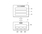
- FIG. 1 is a diagram for explaining a configuration example of a plasma processing system.
- the plasma processing system includes a plasma processing device 1 and a control unit 2.
- the plasma processing system is an example of a substrate processing system
- the plasma processing device 1 is an example of a substrate processing device.
- the plasma processing device 1 includes a plasma processing chamber 10, a substrate support unit 11, and a plasma generation unit 12.
- the plasma processing chamber 10 has a plasma processing space.
- the plasma processing chamber 10 also has at least one gas supply port for supplying at least one processing gas to the plasma processing space, and at least one gas exhaust port for exhausting gas from the plasma processing space.
- the gas supply port is connected to a gas supply unit 20 described later, and the gas exhaust port is connected to an exhaust system 40 described later.
- the substrate support unit 11 is disposed in the plasma processing space, and has a substrate support surface for supporting a substrate.
- the plasma generating unit 12 is configured to generate plasma from at least one processing gas supplied into the plasma processing space.
- the plasma formed in the plasma processing space may be capacitively coupled plasma (CCP), inductively coupled plasma (ICP), ECR plasma (Electron-Cyclotron-resonance plasma), Helicon wave excited plasma (HWP), or surface wave plasma (SWP), etc.
- various types of plasma generating units may be used, including AC (Alternating Current) plasma generating units and DC (Direct Current) plasma generating units.
- the AC signal (AC power) used in the AC plasma generating unit has a frequency in the range of 100 kHz to 10 GHz.
- AC signals include RF (Radio Frequency) signals and microwave signals.
- the RF signal has a frequency in the range of 100 kHz to 150 MHz.
- the control unit 2 processes computer-executable instructions that cause the plasma processing apparatus 1 to perform the various steps described in this disclosure.
- the control unit 2 may be configured to control each element of the plasma processing apparatus 1 to perform the various steps described herein. In one embodiment, a part or all of the control unit 2 may be included in the plasma processing apparatus 1.
- the control unit 2 may include a processing unit 2a1, a storage unit 2a2, and a communication interface 2a3.
- the control unit 2 is realized, for example, by a computer 2a.
- the processing unit 2a1 may be configured to perform various control operations by reading a program from the storage unit 2a2 and executing the read program. This program may be stored in the storage unit 2a2 in advance, or may be acquired via a medium when necessary.
- the acquired program is stored in the storage unit 2a2 and is read from the storage unit 2a2 by the processing unit 2a1 and executed.
- the medium may be various storage media readable by the computer 2a, or may be a communication line connected to the communication interface 2a3.
- the processing unit 2a1 may be a CPU (Central Processing Unit).
- the memory unit 2a2 may include a RAM (Random Access Memory), a ROM (Read Only Memory), a HDD (Hard Disk Drive), a SSD (Solid State Drive), or a combination of these.
- the communication interface 2a3 may communicate with the plasma processing device 1 via a communication line such as a LAN (Local Area Network).
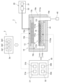
- FIG. 1 is a diagram for explaining an example of the configuration of a capacitively coupled plasma processing device.
- the substrate support 11 includes a main body 111 and a ring assembly 112.
- the main body 111 has a central region 111a for supporting the substrate W and an annular region 111b for supporting the ring assembly 112.
- a wafer is an example of a substrate W.
- the annular region 111b of the main body 111 surrounds the central region 111a of the main body 111 in a plan view.
- the substrate W is disposed on the central region 111a of the main body 111
- the ring assembly 112 is disposed on the annular region 111b of the main body 111 so as to surround the substrate W on the central region 111a of the main body 111. Therefore, the central region 111a is also called a substrate support surface for supporting the substrate W, and the annular region 111b is also called a ring support surface for supporting the ring assembly 112.
- the ring assembly 112 may be disposed on the annular electrostatic chuck or the annular insulating member, or may be disposed on both the electrostatic chuck 1111 and the annular insulating member.
- at least one RF/DC electrode coupled to an RF power source 31 and/or a DC power source 32 described later may be disposed in the ceramic member 1111a.
- the at least one RF/DC electrode functions as a lower electrode.
- the RF/DC electrode is also called a bias electrode.
- the conductive member of the base 1110 and the at least one RF/DC electrode may function as multiple lower electrodes.
- the electrostatic electrode 1111b may function as a lower electrode.
- the substrate support 11 includes at least one lower electrode.
- the ring assembly 112 includes one or more annular members.
- the one or more annular members include one or more edge rings and at least one cover ring.
- the edge rings are formed of a conductive or insulating material, and the cover rings are formed of an insulating material.
- the substrate support 11 may also include a temperature adjustment module configured to adjust at least one of the electrostatic chuck 1111, the ring assembly 112, and the substrate to a target temperature.
- the temperature adjustment module may include a heater, a heat transfer medium, a flow passage 1110a, or a combination thereof.
- a heat transfer fluid such as brine or a gas flows through the flow passage 1110a.
- the flow passage 1110a is formed in the base 1110, and one or more heaters are disposed in the ceramic member 1111a of the electrostatic chuck 1111.
- the substrate support 11 may also include a heat transfer gas supply configured to supply a heat transfer gas to a gap between the back surface of the substrate W and the central region 111a.
- the shower head 13 is configured to introduce at least one processing gas from the gas supply unit 20 into the plasma processing space 10s.
- the shower head 13 has at least one gas supply port 13a, at least one gas diffusion chamber 13b, and multiple gas inlets 13c.
- the processing gas supplied to the gas supply port 13a passes through the gas diffusion chamber 13b and is introduced into the plasma processing space 10s from the multiple gas inlets 13c.
- the shower head 13 also includes at least one upper electrode.
- the gas introduction unit may include, in addition to the shower head 13, one or more side gas injectors (SGI) attached to one or more openings formed in the side wall 10a.
- SGI side gas injectors
- the gas supply unit 20 may include at least one gas source 21 and at least one flow controller 22.
- the gas supply unit 20 is configured to supply at least one process gas from a respective gas source 21 through a respective flow controller 22 to the showerhead 13.
- Each flow controller 22 may include, for example, a mass flow controller or a pressure-controlled flow controller.
- the gas supply unit 20 may include at least one flow modulation device that modulates or pulses the flow rate of the at least one process gas.
- the power supply 30 includes an RF power supply 31 coupled to the plasma processing chamber 10 via at least one impedance matching circuit.
- the RF power supply 31 is configured to supply at least one RF signal (RF power) to at least one lower electrode and/or at least one upper electrode. This causes a plasma to be formed from at least one processing gas supplied to the plasma processing space 10s.
- the RF power supply 31 can function as at least a part of the plasma generating unit 12.
- a bias RF signal to at least one lower electrode, a bias potential is generated on the substrate W, and ion components in the formed plasma can be attracted to the substrate W.
- the RF power supply 31 includes a first RF generating unit 31a and a second RF generating unit 31b.
- the first RF generating unit 31a is coupled to at least one lower electrode and/or at least one upper electrode via at least one impedance matching circuit and configured to generate a source RF signal (source RF power) for plasma generation.
- the source RF signal has a frequency in the range of 10 MHz to 150 MHz.
- the first RF generating unit 31a may be configured to generate multiple source RF signals having different frequencies. The generated one or more source RF signals are supplied to at least one lower electrode and/or at least one upper electrode.
- the second RF generator 31b is coupled to at least one lower electrode via at least one impedance matching circuit and configured to generate a bias RF signal (bias RF power).
- the frequency of the bias RF signal may be the same as or different from the frequency of the source RF signal.
- the bias RF signal has a lower frequency than the frequency of the source RF signal.
- the bias RF signal has a frequency in the range of 100 kHz to 60 MHz.
- the second RF generator 31b may be configured to generate multiple bias RF signals having different frequencies.
- the generated one or more bias RF signals are provided to at least one lower electrode. Also, in various embodiments, at least one of the source RF signal and the bias RF signal may be pulsed.
- the first and second DC signals may be pulsed.
- a sequence of voltage pulses is applied to at least one lower electrode and/or at least one upper electrode.
- the voltage pulses may have a rectangular, trapezoidal, triangular or combination thereof pulse waveform.
- a waveform generator for generating a sequence of voltage pulses from the DC signal is connected between the first DC generator 32a and at least one lower electrode.
- the first DC generator 32a and the waveform generator constitute a voltage pulse generator.
- the second DC generator 32b and the waveform generator constitute a voltage pulse generator
- the voltage pulse generator is connected to at least one upper electrode.
- the voltage pulses may have a positive polarity or a negative polarity.
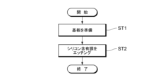
- ⁇ Example of Etching Method> 3 is a flow chart for explaining an example of an etching method (hereinafter also referred to as "this processing method") according to an illustrative embodiment.
- this processing method includes a step ST1 of preparing a substrate, and a step ST2 of etching a silicon-containing film on the substrate to form a recess.
- the processing in each step may be performed in the plasma processing system shown in FIG. 2.
- the control unit 2 controls each part of the plasma processing apparatus 1 to perform this processing method on a substrate W.
- Step ST1 Preparation of substrate
- a substrate W is provided in a plasma processing chamber 10 (hereinafter also referred to as "chamber 10") as shown in Fig. 2.
- the substrate W may be carried into the chamber 10 by a transport arm, placed on a substrate support 11 by a lifter, and held by suction on the substrate support 11.
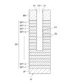
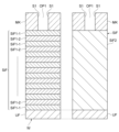
- FIG. 4 is a diagram for explaining an example of the cross-sectional structure of the substrate W provided in process ST1.
- the substrate W includes an undercoat film UF, a silicon-containing film SiF on the undercoat film UF, and a mask MK on the silicon-containing film SiF.
- the substrate W may be used in the manufacture of semiconductor devices.
- the semiconductor devices include, for example, memory devices such as DRAMs and 3D-NAND flash memories, and logic devices.
- the base film UF may be a silicon wafer or an organic film, a dielectric film, a metal film, a semiconductor film, or the like formed on a silicon wafer.
- the base film UF may be configured by stacking multiple films.
- the silicon-containing film SiF is a film to be etched in this processing method.
- the silicon-containing film SiF may contain nitrogen.
- the silicon-containing film SiF may be a laminated film including two or more different types of silicon-containing films.
- the silicon-containing film SiF may be a laminated film in which silicon oxide films SiF1-1 and silicon nitride films SiF1-2 are alternately laminated.
- the silicon-containing film SiF may be a laminated film of 20 layers or more, 50 layers or more, or 100 layers or more.
- the mask MK is a film that functions as a mask in etching the silicon-containing film SiF.
- the mask MK may be a film containing at least one selected from the group consisting of a silicon-containing film, a carbon-containing film, and a metal-containing film.
- the silicon-containing film of the mask MK may be different from the silicon-containing film of the silicon-containing film SiF.
- the carbon-containing film of the mask MK may be an amorphous carbon (ACL) film or a spin-on carbon (SOC) film.
- the metal-containing film of the mask MK may be a film containing at least one selected from the group consisting of tungsten, molybdenum, titanium, and ruthenium.
- the metal-containing film of the mask MK may be a film containing at least one selected from the group consisting of WSi (tungsten silicide), WC (tungsten carbide), WSiC, and WSiN.
- the mask MK may be a single-layer mask consisting of one film, or may be a multilayer mask consisting of two or more films.
- the mask MK may have a sidewall S1 that defines at least one opening OP1 on the film EF to be etched. That is, the mask MK may have an opening OP1.
- the opening OP1 may be a space on the silicon-containing film SiF and may be surrounded by the sidewall S1 of the mask MK.
- the opening OP1 may have any shape when viewed from above the substrate W, i.e., when the substrate W is viewed from the top to the bottom in FIG. 4.
- the shape may be, for example, a circle, an ellipse, a rectangle, a line, or a combination of one or more of these.
- the mask MK may have multiple sidewalls S1, which define multiple openings OP1.
- the multiple openings OP1 may each have a linear shape and be arranged at regular or different intervals to form a line-and-space pattern.
- the multiple openings OP1 may also each have a hole shape and form an array pattern.
- Each of the films constituting the substrate W may be formed by any method.
- the undercoat film UF, silicon-containing film SiF, and mask MK may be formed by CVD, ALD, MLD, PVD, spin coating, or the like.
- the opening OP1 in the mask MK may be formed by etching.
- the opening OP1 in the mask MK may be formed by lithography.
- Each film may be a flat film or may have irregularities.
- the substrate W may further have another film below the undercoat film UF.
- At least a part of the process of forming the undercoat film UF, silicon-containing film SiF, and mask MK of the substrate W may be performed in the chamber 10 as part of step ST1.
- the opening OP1 of the mask MK may be formed by etching in step ST1.
- the mask MK in step ST1 and step ST2 described below may be performed consecutively in the chamber 10.
- the substrate W may be provided in the chamber 10 after all or a part of the film of the substrate W is formed in an apparatus or chamber external to the plasma processing apparatus 1.
- the temperature of the substrate support 11 or the substrate W may be controlled to a given temperature by a temperature control module. Controlling the temperature of the substrate support 11 or the substrate W to a given temperature may include setting the temperature of the heat transfer fluid flowing through the flow path 1110a or the heater temperature to a given temperature, or setting them to a temperature different from the given temperature.
- the given temperature may be, for example, 50°C or less or -50°C or more.
- the given temperature may be 0°C or less.
- the timing at which the temperature of the substrate support 11 or the substrate W starts to be controlled to the given temperature may be before or after the substrate W is provided to the substrate support 11, or may be simultaneous.
- the temperature of the substrate support 11 or the substrate W may be changed in each of the processes ST1, ST2-1, and ST2-2.
- Step ST2 Etching
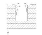
- step ST2 Etching 5 is a diagram for explaining an example of a cross-sectional structure of the substrate W in step ST2.
- the silicon-containing film SiF is etched by plasma generated from a processing gas, and a recess R1 is formed in the silicon-containing film SiF.
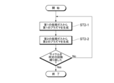
- FIG. 6 is a flow chart showing an example of step ST2.
- step ST2 includes step ST2-1 of generating a first plasma from a first process gas containing a fluorocarbon gas to etch the silicon-containing film, and step ST2-2 of generating a second plasma from a second process gas containing hydrogen fluoride gas to etch the silicon-containing film.
Landscapes
- Drying Of Semiconductors (AREA)
Abstract
Description
<プラズマ処理システムの一例>
図1は、プラズマ処理システムの構成例を説明するための図である。一実施形態において、プラズマ処理システムは、プラズマ処理装置1及び制御部2を含む。プラズマ処理システムは、基板処理システムの一例であり、プラズマ処理装置1は、基板処理装置の一例である。プラズマ処理装置1は、プラズマ処理チャンバ10、基板支持部11及びプラズマ生成部12を含む。プラズマ処理チャンバ10は、プラズマ処理空間を有する。また、プラズマ処理チャンバ10は、少なくとも1つの処理ガスをプラズマ処理空間に供給するための少なくとも1つのガス供給口と、プラズマ処理空間からガスを排出するための少なくとも1つのガス排出口とを有する。ガス供給口は、後述するガス供給部20に接続され、ガス排出口は、後述する排気システム40に接続される。基板支持部11は、プラズマ処理空間内に配置され、基板を支持するための基板支持面を有する。
図3は、一つの例示的実施形態に係るエッチング方法(以下「本処理方法」ともいう。)の一例を説明するためのフローチャートである。図3に示すように、一実施形態において、本処理方法は、基板を準備する工程ST1と、基板のシリコン含有膜をエッチングして凹部を形成する工程ST2と、を含む。各工程における処理は、図2に示すプラズマ処理システムで実行されてよい。以下では、制御部2がプラズマ処理装置1の各部を制御して、基板Wに対して本処理方法を実行する場合を例に説明する。
一実施形態において、工程ST1では、図2に示すように、基板Wがプラズマ処理チャンバ10(以下「チャンバ10」ともいう。)内に提供される。一実施形態において、基板Wは、搬送アームによりチャンバ10内に搬入され、リフターにより基板支持部11に載置され、基板支持部11上に吸着保持されてよい。
図5は、工程ST2における基板Wの断面構造の一例を説明するための図である。一実施形態において、工程ST2では、処理ガスから生成されたプラズマにより、シリコン含有膜SiFがエッチングされ、シリコン含有膜SiFに凹部R1が形成される。
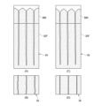
図10(A)は、比較例1におけるシリコン含有膜を含む基板の断面画像を描写した図である。図10(B)は、図10(A)のシリコン含有膜を除去した基板の底部付近の上面画像を描写した図である。図10(C)は、実施例1におけるシリコン含有膜を含む基板の断面画像を描写した図である。図10(D)は、図10(C)のシリコン含有膜を除去した基板の底部付近の上面画像を描写した図である。図10は、走査電子顕微鏡により撮像した画像に基づいている。実施例1及び比較例1では、基板W上のシリコン含有膜SiFに複数のライン状の開口を形成した。
ソースRF信号:5.5kW(40MHz)
バイアス信号:9kV(400kHz)
第2の処理ガス:HFガス、フルオロカーボンガス(C4F6ガス)、O2ガス、ハロゲンガス
処理温度:-20℃
ソースRF信号:5.5kW(40MHz)
バイアス信号:9kV(400kHz)
第1の処理ガス:フルオロカーボンガス(C4F6ガス、C4F8ガス)、O2ガス(第1の処理ガスにおいてフルオロカーボンガスが最大流量)
処理温度:-20℃
ソースRF信号:5.5kW(40MHz)
バイアス信号:9kV(400kHz)
第2の処理ガス:HFガス、フルオロカーボンガス(C4F8ガス)、O2ガス、ハロゲンガス(第2の処理ガスにおいてHFガスが最大流量)
処理温度:-20℃
実施例2及び比較例2では、基板W上のシリコン含有膜に複数のホール状の開口を形成した。
ソースRF信号:5.5kW(40MHz)
バイアス信号:9kV(400kHz)
第2の処理ガス:HFガス、フルオロカーボンガス(C4F6ガス)、ハイドロフルオロカーボンガス(CH2F2ガス)、ハロゲン含有ガス(第2の処理ガスにおいてHFガスが最大流量)
処理温度:0℃
ガス供給時間:1200秒
ソースRF信号:5.5kW(40MHz)
バイアス信号:9kV(400kHz)
第2の処理ガス:HFガス、フルオロカーボンガス(C4F6ガス)、ハイドロフルオロカーボンガス(CH2F2ガス)、ハロゲン含有ガス(第2の処理ガスにおいてHFガスが最大流量)
処理温度:0℃
各サイクルのガス供給時間:60秒
ソースRF信号:5.5kW(40MHz)
バイアス信号:9kV(400kHz)
第1の処理ガス:フルオロカーボンガス(C4F6ガス、C4F8ガス)、O2ガス
処理温度:0℃
各サイクルのガス供給時間:2秒
一実施形態において、基板W上のシリコン含有膜SiFは、シリコン酸化膜、シリコン窒化膜、及び、シリコン酸化膜とシリコン窒化膜を含む積層膜からなる群から選択される少なくとも1種の膜を含むものであってよい。図11は、2種類のシリコン含有膜を有する基板Wの構成例を説明するための図である。一実施形態において、シリコン含有膜SiFは、第1のシリコン含有膜SiF1と、第1のシリコン含有膜SiF1と異なる第2のシリコン含有膜SiF2とを含んでよい。第1のシリコン含有膜SiF1は、上記第1の実施形態と同様の、シリコン酸化膜SiF1-1とシリコン窒化膜SiF1-2とが交互に積層された積層膜であってよい。第2のシリコン含有膜SiF2は、シリコン酸化膜であってよい。シリコン酸化膜は、窒素がドープされていてよい。第2のシリコン含有膜SiF2は、シリコン窒化膜であってよい。
(a)窒素を含有するシリコン含有膜と、前記シリコン含有膜上のマスクとを有する基板を準備する工程であって、前記マスクは少なくとも1つの開口を含む、前記工程と、
(b)前記シリコン含有膜をエッチングして凹部を形成する工程と、を含み、
前記(b)は、
(b1)フルオロカーボンガスを含む第1の処理ガスから第1のプラズマを生成して、前記シリコン含有膜をエッチングする工程であって、前記フルオロカーボンガスは、前記第1の処理ガスの中で最も流量が大きい、前記工程と、
(b2)フッ化水素ガスを含む第2の処理ガスから第2のプラズマを生成して、前記シリコン含有膜をエッチングする工程と、を含む、エッチング方法。
前記フッ化水素ガスは、前記第2の処理ガスの中で最も流量が大きい、付記1に記載のエッチング方法。
前記第1の処理ガスは、フッ化水素ガスを含まない、又は前記第2の処理ガスに含まれる前記フッ化水素ガスの流量より小さい流量のフッ化水素ガスを含む、付記1又は2に記載のエッチング方法。
前記第2の処理ガスは、フルオロカーボンガスを含まない、又は前記第1の処理ガスに含まれる前記フルオロカーボンガスの流量より小さい流量のフルオロカーボンガスを含む、付記1から3のいずれか一項に記載のエッチング方法。
前記第1の処理ガスは、炭素に対するフッ素の組成比が異なる2種以上のフルオロカーボンガスを含む、付記1から4のいずれか一項に記載のエッチング方法。
前記第2の処理ガスは、フルオロカーボンガスを含み、
前記第1の処理ガスは、前記第2の処理ガスの前記フルオロカーボンガスより、炭素に対するフッ素の組成比が大きい前記フルオロカーボンガスを含む、付記1から5のいずれか一項に記載のエッチング方法。
前記第1の処理ガス及び前記第2の処理ガスの少なくとも一方は、酸素含有ガスを含む、付記1から6のいずれか一項に記載のエッチング方法。
前記第1の処理ガス及び前記第2の処理ガスの少なくとも一方は、貴ガス、窒素ガス、金属含有ガス及びハロゲン含有ガスからなる群から選択される少なくとも1種のガスを含む、付記1から7のいずれか一項に記載のエッチング方法。
前記(b1)及び前記(b2)を含むサイクルを複数回繰り返す、付記1から8のいずれか一項に記載のエッチング方法。
前記(b1)の後に前記(b2)を行う、付記9に記載のエッチング方法。
前記(b2)は、前記凹部の側壁に、窒素を含む反応生成物を付着させることを含み、
前記(b1)は、前記凹部の側壁に付着した前記反応生成物を除去することを含む、付記9又は10に記載のエッチング方法。
前記(b1)は、前記凹部の側壁に炭素含有膜を形成することを含む、付記9から11のいずれか一項に記載のエッチング方法。
前記(b1)後における前記凹部のラインエッジラフネスは、直前に行われた前記(b2)後における前記凹部のラインエッジラフネスより小さい、付記9から12のいずれか一項に記載のエッチング方法。
前記(b1)の処理時間は、前記(b2)の処理時間と同じか、それより短い、付記9から13のいずれか一項に記載のエッチング方法。
前記(b1)の処理時間は、前記(b2)の処理時間より長い、付記9から13のいずれか一項に記載のエッチング方法。
前記凹部のエッチングが進むにつれて、前記(b1)の処理時間に対する前記(b2)の処理時間の比率を変更する、付記9から15のいずれか一項に記載のエッチング方法。
前記シリコン含有膜は、シリコン酸化膜、シリコン窒化膜、及び、シリコン酸化膜とシリコン窒化膜を含む積層膜からなる群から選択される少なくとも1種の膜を含む、付記1から16のいずれか一項に記載のエッチング方法。
前記シリコン含有膜は、第1のシリコン含有膜と、前記第1のシリコン含有膜と異なる第2のシリコン含有膜とを含み、
前記第1のシリコン含有膜は、シリコン酸化膜とシリコン窒化膜が交互に積層された積層膜であり、
前記第2のシリコン含有膜は、シリコン酸化膜である、付記1から17のいずれか一項に記載のエッチング方法。
前記マスクは、前記シリコン含有膜と異なるシリコン含有膜、炭素含有膜及び金属含有膜からなる群から選択される少なくとも1種の膜を含む、付記1から18のいずれか一項に記載のエッチング方法。
チャンバと、前記チャンバ内の基板支持部と、プラズマ生成部と、制御部とを備える基板処理装置であって、
前記制御部は、
(a)窒素を含有するシリコン含有膜と、前記シリコン含有膜上のマスクとを有する基板を前記チャンバ内の前記基板支持部上に準備する制御であって、前記マスクは少なくとも1つの開口を含む、前記制御と、
(b)前記基板支持部上の前記基板の前記シリコン含有膜をエッチングして凹部を形成する制御と、を実行し、
前記(b)の制御は、
(b1)フルオロカーボンガスを含む第1の処理ガスから第1のプラズマを前記プラズマ生成部により生成して、前記シリコン含有膜をエッチングする制御であって、前記フルオロカーボンガスは、前記第1の処理ガスの中で最も流量が大きい、前記制御と、
(b2)フッ化水素ガスを含む第2の処理ガスから第2のプラズマを前記プラズマ生成部により生成して、前記シリコン含有膜をエッチングする制御と、を実行するように構成されている、基板処理装置。
Claims (20)
- (a)窒素を含有するシリコン含有膜と、前記シリコン含有膜上のマスクとを有する基板を準備する工程であって、前記マスクは少なくとも1つの開口を含む、前記工程と、
(b)前記シリコン含有膜をエッチングして凹部を形成する工程と、を含み、
前記(b)は、
(b1)フルオロカーボンガスを含む第1の処理ガスから第1のプラズマを生成して、前記シリコン含有膜をエッチングする工程であって、前記フルオロカーボンガスは、前記第1の処理ガスの中で最も流量が大きい、前記工程と、
(b2)フッ化水素ガスを含む第2の処理ガスから第2のプラズマを生成して、前記シリコン含有膜をエッチングする工程と、を含む、エッチング方法。 - 前記フッ化水素ガスは、前記第2の処理ガスの中で最も流量が大きい、請求項1に記載のエッチング方法。
- 前記第1の処理ガスは、フッ化水素ガスを含まない、又は前記第2の処理ガスに含まれる前記フッ化水素ガスの流量より小さい流量のフッ化水素ガスを含む、請求項1に記載のエッチング方法。
- 前記第2の処理ガスは、フルオロカーボンガスを含まない、又は前記第1の処理ガスに含まれる前記フルオロカーボンガスの流量より小さい流量のフルオロカーボンガスを含む、請求項1に記載のエッチング方法。
- 前記第1の処理ガスは、炭素に対するフッ素の組成比が異なる2種以上のフルオロカーボンガスを含む、請求項1に記載のエッチング方法。
- 前記第2の処理ガスは、フルオロカーボンガスを含み、
前記第1の処理ガスは、前記第2の処理ガスの前記フルオロカーボンガスより、炭素に対するフッ素の組成比が大きい前記フルオロカーボンガスを含む、請求項1に記載のエッチング方法。 - 前記第1の処理ガス及び前記第2の処理ガスの少なくとも一方は、酸素含有ガスを含む、請求項1に記載のエッチング方法。
- 前記第1の処理ガス及び前記第2の処理ガスの少なくとも一方は、貴ガス、窒素ガス、金属含有ガス及びハロゲン含有ガスからなる群から選択される少なくとも1種のガスを含む、請求項1に記載のエッチング方法。
- 前記(b1)及び前記(b2)を含むサイクルを複数回繰り返す、請求項1に記載のエッチング方法。
- 前記(b1)の後に前記(b2)を行う、請求項9に記載のエッチング方法。
- 前記(b2)は、前記凹部の側壁に、窒素を含む反応生成物を付着させることを含み、
前記(b1)は、前記凹部の側壁に付着した前記反応生成物を除去することを含む、請求項9に記載のエッチング方法。 - 前記(b1)は、前記凹部の側壁に炭素含有膜を形成することを含む、請求項9に記載のエッチング方法。
- 前記(b1)後における前記凹部のラインエッジラフネスは、直前に行われた前記(b2)後における前記凹部のラインエッジラフネスより小さい、請求項9に記載のエッチング方法。
- 前記(b1)の処理時間は、前記(b2)の処理時間と同じか、それより短い、請求項9に記載のエッチング方法。
- 前記(b1)の処理時間は、前記(b2)の処理時間より長い、請求項9に記載のエッチング方法。
- 前記凹部のエッチングが進むにつれて、前記(b1)の処理時間に対する前記(b2)の処理時間の比率を変更する、請求項9に記載のエッチング方法。
- 前記シリコン含有膜は、シリコン酸化膜、シリコン窒化膜、及び、シリコン酸化膜とシリコン窒化膜を含む積層膜からなる群から選択される少なくとも1種の膜を含む、請求項1に記載のエッチング方法。
- 前記シリコン含有膜は、第1のシリコン含有膜と、前記第1のシリコン含有膜と異なる第2のシリコン含有膜とを含み、
前記第1のシリコン含有膜は、シリコン酸化膜とシリコン窒化膜が交互に積層された積層膜であり、
前記第2のシリコン含有膜は、シリコン酸化膜である、請求項1に記載のエッチング方法。 - 前記マスクは、前記シリコン含有膜と異なるシリコン含有膜、炭素含有膜及び金属含有膜からなる群から選択される少なくとも1種の膜を含む、請求項1に記載のエッチング方法。
- チャンバと、前記チャンバ内の基板支持部と、プラズマ生成部と、制御部とを備える基板処理装置であって、
前記制御部は、
(a)窒素を含有するシリコン含有膜と、前記シリコン含有膜上のマスクとを有する基板を前記チャンバ内の前記基板支持部上に準備する制御であって、前記マスクは少なくとも1つの開口を含む、前記制御と、
(b)前記基板支持部上の前記基板の前記シリコン含有膜をエッチングして凹部を形成する制御と、を実行し、
前記(b)の制御は、
(b1)フルオロカーボンガスを含む第1の処理ガスから第1のプラズマを前記プラズマ生成部により生成して、前記シリコン含有膜をエッチングする制御であって、前記フルオロカーボンガスは、前記第1の処理ガスの中で最も流量が大きい、前記制御と、
(b2)フッ化水素ガスを含む第2の処理ガスから第2のプラズマを前記プラズマ生成部により生成して、前記シリコン含有膜をエッチングする制御と、を実行するように構成されている、基板処理装置。
Priority Applications (2)
| Application Number | Priority Date | Filing Date | Title |
|---|---|---|---|
| CN202480079876.1A CN122423355A (zh) | 2023-12-27 | 2024-11-19 | 蚀刻方法和基板处理装置 |
| TW113148608A TW202531380A (zh) | 2023-12-27 | 2024-12-13 | 蝕刻方法及基板處理裝置 |
Applications Claiming Priority (2)
| Application Number | Priority Date | Filing Date | Title |
|---|---|---|---|
| JP2023-220955 | 2023-12-27 | ||
| JP2023220955 | 2023-12-27 |
Publications (1)
| Publication Number | Publication Date |
|---|---|
| WO2025142198A1 true WO2025142198A1 (ja) | 2025-07-03 |
Family
ID=96218827
Family Applications (1)
| Application Number | Title | Priority Date | Filing Date |
|---|---|---|---|
| PCT/JP2024/040904 Pending WO2025142198A1 (ja) | 2023-12-27 | 2024-11-19 | エッチング方法及び基板処理装置 |
Country Status (3)
| Country | Link |
|---|---|
| CN (1) | CN122423355A (ja) |
| TW (1) | TW202531380A (ja) |
| WO (1) | WO2025142198A1 (ja) |
Citations (7)
| Publication number | Priority date | Publication date | Assignee | Title |
|---|---|---|---|---|
| WO2020090451A1 (ja) * | 2018-11-02 | 2020-05-07 | セントラル硝子株式会社 | ドライエッチング方法 |
| JP2022032965A (ja) * | 2020-08-12 | 2022-02-25 | 東京エレクトロン株式会社 | エッチング方法及びプラズマエッチング装置 |
| JP2022101060A (ja) * | 2020-12-24 | 2022-07-06 | 東京エレクトロン株式会社 | 基板処理方法及び基板処理装置 |
| JP2023048519A (ja) * | 2021-09-28 | 2023-04-07 | 東京エレクトロン株式会社 | プラズマ処理方法及びプラズマ処理装置 |
| JP2023063106A (ja) * | 2021-10-22 | 2023-05-09 | 東京エレクトロン株式会社 | プラズマ処理方法及びプラズマ処理システム |
| JP2023109497A (ja) * | 2022-01-27 | 2023-08-08 | 東京エレクトロン株式会社 | エッチング方法及びプラズマ処理装置 |
| JP2023155483A (ja) * | 2021-12-03 | 2023-10-20 | 東京エレクトロン株式会社 | プラズマ処理装置、エッチング方法、半導体デバイスの製造方法、プログラム及び記憶媒体 |
-
2024
- 2024-11-19 CN CN202480079876.1A patent/CN122423355A/zh active Pending
- 2024-11-19 WO PCT/JP2024/040904 patent/WO2025142198A1/ja active Pending
- 2024-12-13 TW TW113148608A patent/TW202531380A/zh unknown
Patent Citations (7)
| Publication number | Priority date | Publication date | Assignee | Title |
|---|---|---|---|---|
| WO2020090451A1 (ja) * | 2018-11-02 | 2020-05-07 | セントラル硝子株式会社 | ドライエッチング方法 |
| JP2022032965A (ja) * | 2020-08-12 | 2022-02-25 | 東京エレクトロン株式会社 | エッチング方法及びプラズマエッチング装置 |
| JP2022101060A (ja) * | 2020-12-24 | 2022-07-06 | 東京エレクトロン株式会社 | 基板処理方法及び基板処理装置 |
| JP2023048519A (ja) * | 2021-09-28 | 2023-04-07 | 東京エレクトロン株式会社 | プラズマ処理方法及びプラズマ処理装置 |
| JP2023063106A (ja) * | 2021-10-22 | 2023-05-09 | 東京エレクトロン株式会社 | プラズマ処理方法及びプラズマ処理システム |
| JP2023155483A (ja) * | 2021-12-03 | 2023-10-20 | 東京エレクトロン株式会社 | プラズマ処理装置、エッチング方法、半導体デバイスの製造方法、プログラム及び記憶媒体 |
| JP2023109497A (ja) * | 2022-01-27 | 2023-08-08 | 東京エレクトロン株式会社 | エッチング方法及びプラズマ処理装置 |
Also Published As
| Publication number | Publication date |
|---|---|
| TW202531380A (zh) | 2025-08-01 |
| CN122423355A (zh) | 2026-07-17 |
Similar Documents
| Publication | Publication Date | Title |
|---|---|---|
| TW202437384A (zh) | 蝕刻方法及電漿處理裝置 | |
| JP7721458B2 (ja) | プラズマ処理方法及びプラズマ処理システム | |
| JP7675033B2 (ja) | エッチング方法及びプラズマ処理装置 | |
| TW202412101A (zh) | 蝕刻方法及電漿處理裝置 | |
| JP2023109496A (ja) | エッチング方法及びプラズマ処理装置 | |
| CN115148593A (zh) | 蚀刻方法和蚀刻处理装置 | |
| TW202531380A (zh) | 蝕刻方法及基板處理裝置 | |
| WO2024247866A1 (ja) | エッチング方法、dramキャパシタの製造方法及びプラズマ処理装置 | |
| WO2025004625A1 (ja) | エッチング方法及びプラズマ処理装置 | |
| US20250174462A1 (en) | Substrate processing method and substrate processing system | |
| US20240213032A1 (en) | Etching method and plasma processing apparatus | |
| WO2025150294A1 (ja) | 基板処理方法及び基板処理装置 | |
| WO2024180921A1 (ja) | エッチング方法及びプラズマ処理装置 | |
| WO2025079458A1 (ja) | エッチング方法及びエッチング装置 | |
| WO2025177876A1 (ja) | 基板処理方法及び基板処理システム | |
| WO2025182550A1 (ja) | エッチング方法及びエッチング装置 | |
| WO2025150267A1 (ja) | プラズマ処理装置及びプラズマ処理方法 | |
| WO2024171666A1 (ja) | エッチング方法及びプラズマ処理装置 | |
| JP2025071859A (ja) | エッチング方法及びプラズマ処理システム | |
| WO2024172109A1 (ja) | プラズマ処理装置及びプラズマ処理方法 | |
| WO2025177874A1 (ja) | プラズマエッチング装置及び基板処理装置 | |
| JP2025089743A (ja) | エッチング方法 | |
| TW202439445A (zh) | 電漿處理方法及電漿處理裝置 | |
| JP2024010798A (ja) | プラズマ処理方法及びプラズマ処理システム | |
| WO2025150427A1 (ja) | エッチング方法及びプラズマ処理システム |
Legal Events
| Date | Code | Title | Description |
|---|---|---|---|
| 121 | Ep: the epo has been informed by wipo that ep was designated in this application |
Ref document number: 24912091 Country of ref document: EP Kind code of ref document: A1 |
|
| ENP | Entry into the national phase |
Ref document number: 2025566335 Country of ref document: JP Kind code of ref document: A |
|
| WWE | Wipo information: entry into national phase |
Ref document number: 2025566335 Country of ref document: JP |
|
| WWE | Wipo information: entry into national phase |
Ref document number: 1020267022972 Country of ref document: KR |
|
| WWE | Wipo information: entry into national phase |
Ref document number: 11202604222R Country of ref document: SG |
|
| WWP | Wipo information: published in national office |
Ref document number: 11202604222R Country of ref document: SG |