WO2025142138A1 - プラズマ処理装置 - Google Patents
プラズマ処理装置 Download PDFInfo
- Publication number
- WO2025142138A1 WO2025142138A1 PCT/JP2024/039396 JP2024039396W WO2025142138A1 WO 2025142138 A1 WO2025142138 A1 WO 2025142138A1 JP 2024039396 W JP2024039396 W JP 2024039396W WO 2025142138 A1 WO2025142138 A1 WO 2025142138A1
- Authority
- WO
- WIPO (PCT)
- Prior art keywords
- time
- power
- processing unit
- plasma processing
- processing apparatus
- Prior art date
- Legal status (The legal status is an assumption and is not a legal conclusion. Google has not performed a legal analysis and makes no representation as to the accuracy of the status listed.)
- Pending
Links
Images



Classifications
-
- H—ELECTRICITY
- H10—SEMICONDUCTOR DEVICES; ELECTRIC SOLID-STATE DEVICES NOT OTHERWISE PROVIDED FOR
- H10P—GENERIC PROCESSES OR APPARATUS FOR THE MANUFACTURE OR TREATMENT OF DEVICES COVERED BY CLASS H10
- H10P50/00—Etching of wafers, substrates or parts of devices
- H10P50/20—Dry etching; Plasma etching; Reactive-ion etching
- H10P50/24—Dry etching; Plasma etching; Reactive-ion etching of semiconductor materials
- H10P50/242—Dry etching; Plasma etching; Reactive-ion etching of semiconductor materials of Group IV materials
Definitions
- An exemplary embodiment of the present disclosure relates to a plasma processing apparatus.
- This disclosure provides a technology that can reduce the impact of wear on components in a chamber of a plasma processing apparatus on plasma processing of a substrate.
- a plasma processing apparatus includes a chamber, a substrate support disposed in the chamber, the substrate support including a lower electrode, an edge ring disposed to surround a substrate on the substrate support, an upper electrode disposed above the substrate support, a first gas supply configured to supply a first gas into the chamber, an RF power supply configured to supply RF power to the upper electrode or the lower electrode to generate plasma from the first gas in the chamber, a DC power supply configured to apply a DC voltage to the edge ring, a first counter configured to count a first time according to an operation time of the RF power supply and to reset the first time by replacing the upper electrode, a second counter configured to count a second time according to an operation time of the RF power supply and to reset the second time by replacing the edge ring, a first processing unit configured to gradually change at least one of the RF power and the first gas according to the first time, and a second processing unit configured to gradually change the DC voltage according to the second time.
- a technology can be provided in a plasma processing apparatus that can reduce the effect of plasma processing of a substrate caused by wear of components in the chamber.
- FIG. 1 is a diagram for explaining a configuration example of a plasma processing system.
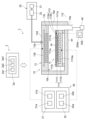
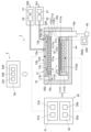
- 1 is a diagram for explaining a configuration example of a plasma processing apparatus according to a first embodiment
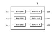
- FIG. 4 is a diagram for explaining a configuration example of a control unit.
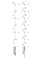
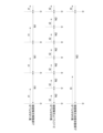
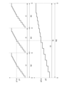
- 11A and 11B are diagrams for explaining an example of the replacement period and count time of the upper electrode and the edge ring.
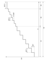
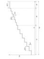
- FIG. 11 is a diagram for explaining an example of changing RF power stepwise according to a first time period.
- FIG. 11 is a diagram for explaining an example of changing the flow rate of the first gas stepwise according to a first time.
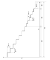
- FIG. 11 is a diagram for explaining an example of changing the DC voltage stepwise according to the second time.
- FIG. 13 is a diagram for explaining a configuration example of a plasma processing apparatus according to a second embodiment.
- FIG. 4 is a diagram for explaining a configuration example of a control unit.
- 11A and 11B are diagrams for explaining an example of replacement periods and count times for an upper electrode, an edge ring, and an upper annular member.
- FIG. 11 is a diagram for explaining an example of changing the flow rate of the second gas stepwise in accordance with a third time period.
- FIG. 11 is a diagram for explaining an example in which the first power value and the second power value are changed stepwise according to a third time period.
- a plasma processing apparatus in one exemplary embodiment, includes a chamber, a substrate support disposed in the chamber, the substrate support including a lower electrode, an edge ring disposed to surround the substrate on the substrate support, an upper electrode disposed above the substrate support, a first gas supply configured to supply a first gas into the chamber, an RF power supply configured to supply RF power to the upper electrode or the lower electrode to generate plasma from the first gas in the chamber, a DC power supply configured to apply a DC voltage to the edge ring, a first counter configured to count a first time according to an operation time of the RF power supply and to reset the first time by replacing the upper electrode, a second counter configured to count a second time according to an operation time of the RF power supply and to reset the second time by replacing the edge ring, a first processing unit configured to gradually change at least one of the RF power and the first gas according to the first time, and a second processing unit configured to gradually change the DC voltage according to the second time.
- the replacement period of the edge ring is different from the replacement period of the upper electrode.
- the first processing unit is configured to incrementally increase the RF power according to a first time
- the second processing unit is configured to incrementally increase the DC voltage according to a second time.
- the first processing unit is configured to incrementally reduce the flow rate of the first gas in response to a first time period.
- the plasma processing apparatus further includes a second gas supply unit
- the upper electrode has a central region and an annular region in a plan view
- the first gas supply unit is configured to supply a first gas into the chamber via the central region
- the second gas supply unit is configured to supply a second gas into the chamber via the annular region.
- the plasma processing apparatus further includes an annular member arranged to surround the upper electrode or the edge ring, a third counter configured to count a third time according to the operation time of the RF power supply and to reset the third time by replacing the annular member, and a third processing unit configured to gradually change the flow rate of the second gas according to the third time.
- the plasma processing apparatus further includes an annular member arranged to surround the upper electrode, and a third counter configured to count a third time according to the operation time of the RF power supply and to reset the third time by replacing the annular member, and the first processing unit is configured to gradually change the RF power according to the first time and the third time.
- the first processing unit is configured to add a first power value corresponding to a first time and a second power value corresponding to a third time to a power level of the RF power.
- the first processing unit is configured to add a first power value to the power level of the RF power for each step in the first interval, and to add a second power value, different from the first power value, to the power level of the RF power for each step in the second interval.
- the second processing unit is configured to maintain a constant voltage level during the third interval.
- the first processing unit is configured to subtract a first flow rate value from the flow rate of the first gas for each step in the first section, and to subtract a second flow rate value, different from the first flow rate value, from the flow rate of the first gas for each step in the second section.
- the first processing section is configured to maintain a constant flow rate in the third section.
- a plasma processing apparatus in one exemplary embodiment, includes a chamber, an RF power supply configured to generate RF power to generate a plasma in the chamber, a first consumable part disposed in the chamber, a second consumable part disposed in the chamber, a first counter configured to count a first time according to an operating time of the RF power supply and to reset the first time by replacing the first consumable part, a second counter configured to count a second time according to an operating time of the RF power supply and to reset the second time by replacing the second consumable part, a first processing unit configured to gradually change a first process parameter according to the first time, and a second processing unit configured to gradually change a second process parameter according to the second time.
- the replacement period of the first consumable part is different from the replacement period of the second consumable part.
- the plasma processing apparatus further includes a third consumable part disposed in the chamber, and a third counter configured to count a third time according to an operating time of the RF power supply and to reset the third time by replacing the third consumable part, and the first processing unit is configured to add or subtract a first value according to the first time and a second value according to the third time to or from the first process parameter.
- the first processing unit is configured to add or subtract a first value to the first process parameter for each stage in the first interval, and to add or subtract a second value to the first process parameter for each stage in the second interval.
- the second processing unit is configured to add or subtract a first value to the second process parameter for each stage in the first interval, and to add or subtract a second value to the second process parameter for each stage in the second interval.
- a plasma processing apparatus in one exemplary embodiment, includes a chamber, an RF power supply configured to generate RF power to generate plasma in the chamber, a consumable part disposed in the chamber, a counter configured to count a first time according to an operating time of the RF power supply and to reset the first time by replacing the consumable part, and a processing unit configured to gradually change a first process parameter according to the first time, wherein the processing unit is configured to add or subtract a first value to the first process parameter for each step in a first interval, and to add or subtract a second value to the first process parameter for each step in a second interval.
- FIG. 1 is a diagram for explaining a configuration example of a plasma processing system.
- the plasma processing system includes a plasma processing device 1 and a control unit 2.
- the plasma processing system is an example of a substrate processing system
- the plasma processing device 1 is an example of a substrate processing device.
- the plasma processing device 1 includes a plasma processing chamber 10, a substrate support unit 11, and a plasma generation unit 12.
- the plasma processing chamber 10 has a plasma processing space.
- the plasma processing chamber 10 also has at least one gas supply port for supplying at least one processing gas to the plasma processing space, and at least one gas exhaust port for exhausting gas from the plasma processing space.
- the gas supply port is connected to a gas supply unit 20 described later, and the gas exhaust port is connected to an exhaust system 40 described later.
- the substrate support unit 11 is disposed in the plasma processing space, and has a substrate support surface for supporting a substrate.
- the plasma generating unit 12 is configured to generate plasma from at least one processing gas supplied into the plasma processing space.
- the plasma formed in the plasma processing space may be capacitively coupled plasma (CCP), inductively coupled plasma (ICP), ECR plasma (Electron-Cyclotron-resonance plasma), Helicon wave excited plasma (HWP: Helicon Wave Plasma), or surface wave plasma (SWP: Surface Wave Plasma), etc.
- various types of plasma generating units may be used, including AC (Alternating Current) plasma generating units and DC (Direct Current) plasma generating units.
- the AC signal (AC power) used in the AC plasma generating unit has a frequency in the range of 100 kHz to 10 GHz.
- AC signals include RF (Radio Frequency) signals and microwave signals.
- the RF signal has a frequency in the range of 100 kHz to 150 MHz.
- the control unit 2 processes computer-executable instructions that cause the plasma processing apparatus 1 to perform the various steps described in this disclosure.
- the control unit 2 may be configured to control each element of the plasma processing apparatus 1 to perform the various steps described herein. In one embodiment, a part or all of the control unit 2 may be included in the plasma processing apparatus 1.
- the control unit 2 may include a processing unit 2a1, a storage unit 2a2, and a communication interface 2a3.
- the control unit 2 is realized, for example, by a computer 2a.
- the processing unit 2a1 may be configured to perform various control operations by reading a program from the storage unit 2a2 and executing the read program. This program may be stored in the storage unit 2a2 in advance, or may be acquired via a medium when necessary.
- the acquired program is stored in the storage unit 2a2 and is read from the storage unit 2a2 by the processing unit 2a1 and executed.
- the medium may be various storage media readable by the computer 2a, or may be a communication line connected to the communication interface 2a3.
- the processing unit 2a1 may be a CPU (Central Processing Unit).
- the memory unit 2a2 may include a RAM (Random Access Memory), a ROM (Read Only Memory), a HDD (Hard Disk Drive), a SSD (Solid State Drive), or a combination of these.
- the communication interface 2a3 may communicate with the plasma processing device 1 via a communication line such as a LAN (Local Area Network).
- FIG. 1 is a diagram for explaining an example of the configuration of a capacitively coupled plasma processing device.
- the capacitively coupled plasma processing apparatus 1 includes a plasma processing chamber 10 (also simply referred to as the "chamber"), a gas supply unit 20, a power supply 30, and an exhaust system 40.
- the plasma processing apparatus 1 also includes a substrate support unit 11 and a gas inlet unit.
- the gas inlet unit is configured to introduce at least one processing gas into the plasma processing chamber 10.
- the gas inlet unit includes a shower head 13.
- the substrate support unit 11 is disposed in the plasma processing chamber 10.
- the shower head 13 is disposed above the substrate support unit 11. In one embodiment, the shower head 13 constitutes at least a part of the ceiling of the plasma processing chamber 10.
- the plasma processing chamber 10 has a plasma processing space 10s defined by the shower head 13, the sidewall 10a of the plasma processing chamber 10, and the substrate support unit 11.
- the plasma processing chamber 10 is grounded.
- the shower head 13 and the substrate support unit 11 are electrically insulated from the housing of the plasma processing chamber 10.
- the substrate support 11 includes a main body 111 and a ring assembly 112.
- the main body 111 has a central region 111a for supporting the substrate W and an annular region 111b for supporting the ring assembly 112.
- a wafer is an example of a substrate W.
- the annular region 111b of the main body 111 surrounds the central region 111a of the main body 111 in a plan view.
- the substrate W is disposed on the central region 111a of the main body 111
- the ring assembly 112 is disposed on the annular region 111b of the main body 111 so as to surround the substrate W on the central region 111a of the main body 111. Therefore, the central region 111a is also called a substrate support surface for supporting the substrate W, and the annular region 111b is also called a ring support surface for supporting the ring assembly 112.
- the main body 111 includes a base 1110 and an electrostatic chuck 1111.
- the base 1110 includes a conductive member.
- the conductive member of the base 1110 may function as a lower electrode.
- the electrostatic chuck 1111 is disposed on the base 1110.
- the electrostatic chuck 1111 includes a ceramic member 1111a and an electrostatic electrode 1111b disposed within the ceramic member 1111a.
- the ceramic member 1111a has a central region 111a. In one embodiment, the ceramic member 1111a also has an annular region 111b. Note that other members surrounding the electrostatic chuck 1111, such as an annular electrostatic chuck or an annular insulating member, may have the annular region 111b.
- the ring assembly 112 may be disposed on the annular electrostatic chuck or the annular insulating member, or may be disposed on both the electrostatic chuck 1111 and the annular insulating member.
- at least one RF/DC electrode coupled to an RF power source 31 and/or a DC power source 32 described later may be disposed in the ceramic member 1111a.
- the at least one RF/DC electrode functions as a lower electrode.
- the RF/DC electrode is also called a bias electrode.
- the conductive member of the base 1110 and the at least one RF/DC electrode may function as multiple lower electrodes.
- the electrostatic electrode 1111b may function as a lower electrode.
- the substrate support 11 includes at least one lower electrode.
- the shower head 13 is configured to introduce at least one processing gas from the gas supply unit 20 into the plasma processing space 10s.
- the shower head 13 has at least one gas supply port 13a, at least one gas diffusion chamber 13b, and multiple gas inlets 13c.
- the processing gas supplied to the gas supply port 13a passes through the gas diffusion chamber 13b and is introduced into the plasma processing space 10s from the multiple gas inlets 13c.
- the shower head 13 also includes at least one upper electrode.
- the gas introduction unit may include, in addition to the shower head 13, one or more side gas injectors (SGI) attached to one or more openings formed in the sidewall 10a.
- SGI side gas injectors
- the flow rate value that is reduced for each stage, the time of each stage, and the number of stages may become smaller as the first time t1 progresses (sections S4 to S6 progress). In this way, even if the upper electrode 13d gradually wears out, the line width (CD) of the film to be etched in the etching process is maintained within an appropriate range.
- the first processing unit 252 is configured to add a first power value p1 corresponding to the first time t1 and a second power value p2 corresponding to the third time t3 to the power level of the RF power Prf.
- the first power value p1 increases stepwise according to the first time t1
- the second power value p2 increases stepwise according to the third time t3.
- the RF power can be appropriately adjusted based on multiple usage times of multiple consumable parts.
- the first counter 250 resets the first time t1 when the upper electrode 13d is replaced and counts the usage time of the upper electrode 13d, but may be reset when a first consumable part other than the upper electrode 13d is replaced and counts the usage time of the other first consumable part.
- the second counter resets the second time t2 when the edge ring 112a is replaced and counts the usage time of the edge ring 112a, but may be reset when a second consumable part other than the edge ring 112a is replaced and counts the usage time of the other second consumable part.
- the third counter resets the third time when the upper annular member 300 or the cover ring 112b is replaced and counts the usage time of the upper electrode 13d, but may be reset when a third consumable part other than the upper annular member 300 or the cover ring 112b is replaced and counts the usage time of the other third consumable part.
- the processing unit changes the RF power, the DC voltage, the flow rate of the first gas, and the flow rate of the second gas according to the time counted by the counter, but other process parameters may be changed.
- the process parameters may include the bias power supplied to the lower electrode, the pulsed voltage applied to the lower electrode, the temperature of the substrate support or the substrate, the DC voltage applied to the upper electrode, etc.
- the number of counters configured to count time according to the operating time of the RF power supply, such as the first to third counters 250, 251, 400, and to reset the time by replacing a consumable part, and the number of processing units configured to gradually change process parameters according to the time counted by the counter, such as the first to third processing units 252, 253, 401, may be one or four or more.
- the number of sections may be one, two, three, or four or more.
- the value to be added to or subtracted from the process parameters for each stage may be manually input and set in the processing unit.
- the number of sections and the time (length) of each section may be manually input and set in the processing unit.
- the first counter may be configured to count the first number of substrates processed according to the operation time of the RF power supply, and the first number of substrates processed is reset by replacement of the first consumable part
- the second counter may be configured to count the second number of substrates processed according to the operation time of the RF power supply, and the second number of substrates processed is reset by replacement of the second consumable part
- the first processing unit may be configured to change the first process parameter in stages according to the first number of substrates processed
- the second processing unit may be configured to change the second process parameter in stages according to the second number of substrates processed.
- the plasma processing apparatus is not limited to a capacitively coupled plasma processing apparatus, but may be another type of plasma processing apparatus, such as a plasma processing apparatus that generates an inductively coupled plasma, a plasma processing apparatus that generates an ECR plasma, a plasma processing apparatus that generates a helicon wave excited plasma, or a plasma processing apparatus that generates a surface wave plasma.
- the time is counted according to the operation time of the RF power supply, but this is not limited to this.
- the time may be counted according to various counters built into the plasma processing apparatus 1.
- the plasma processing apparatus 1 has been described as an example, but the present invention is not limited to this.
- the present invention may be applied to a substrate processing apparatus that does not use plasma.
- the substrate processing apparatus includes a chamber, a first consumable part disposed in the chamber, and a second consumable part disposed in the chamber.
- the substrate processing apparatus further includes a first counter, a second counter, a first processing unit, and a second processing unit.
- the first counter is configured to count a first time according to an operating time of the substrate processing apparatus, and to reset the first time by replacing the first consumable part.
- the second counter is configured to count a second time according to an operating time of the substrate processing apparatus, and to reset the second time by replacing the second consumable part.
- the first processing unit is configured to change the first process parameter in stages according to the first time.
- the second processing unit is configured to change the second process parameter in stages according to the second time.
- the substrate processing apparatus includes a chamber and a consumable part disposed in the chamber.
- the substrate processing apparatus further includes a counter and a processing unit.
- the counter is configured to count a first time according to an operating time of the substrate processing apparatus and to reset the first time by replacing the consumable part.
- the processing unit is configured to change a first process parameter in stages according to the first time. Specifically, the processing unit is configured to add or subtract a first value to the first process parameter for each stage in a first interval, and to add or subtract a second value to the first process parameter for each stage in a second interval.
- the operating time of the substrate processing apparatus can be obtained based on various counters built into the substrate processing apparatus.
- a chamber A chamber; a substrate support disposed within the chamber, the substrate support including a lower electrode; an edge ring disposed to surround the substrate on the substrate support; an upper electrode disposed above the substrate support; a first gas supply configured to supply a first gas into the chamber; an RF power source configured to supply RF power to the upper electrode or the lower electrode to generate a plasma from the first gas in the chamber; a DC power supply configured to apply a DC voltage to the edge ring; a first counter configured to count a first time according to an operation time of the RF power supply and to reset the first time by replacing the upper electrode; a second counter configured to count a second time according to an operation time of the RF power supply and to reset the second time by replacing the edge ring; a first processing unit configured to gradually change at least one of the RF power and the first gas in response to the first time; A second processing unit configured to change the DC voltage stepwise in response to the second time;
- a plasma processing apparatus comprising:
- the first processing unit is configured to increase the RF power stepwise in response to the first time; 3.
- the second processing unit is configured to increase the DC voltage stepwise in accordance with the second time period.
- the plasma processing apparatus of claim 5 further comprising: a third processing unit configured to change a flow rate of the second gas in a stepwise manner in response to the third time period.
Landscapes
- Plasma Technology (AREA)
- Chemical Vapour Deposition (AREA)
Abstract
Description
<プラズマ処理システムの一例>
図1は、プラズマ処理システムの構成例を説明するための図である。一実施形態において、プラズマ処理システムは、プラズマ処理装置1及び制御部2を含む。プラズマ処理システムは、基板処理システムの一例であり、プラズマ処理装置1は、基板処理装置の一例である。プラズマ処理装置1は、プラズマ処理チャンバ10、基板支持部11及びプラズマ生成部12を含む。プラズマ処理チャンバ10は、プラズマ処理空間を有する。また、プラズマ処理チャンバ10は、少なくとも1つの処理ガスをプラズマ処理空間に供給するための少なくとも1つのガス供給口と、プラズマ処理空間からガスを排出するための少なくとも1つのガス排出口とを有する。ガス供給口は、後述するガス供給部20に接続され、ガス排出口は、後述する排気システム40に接続される。基板支持部11は、プラズマ処理空間内に配置され、基板を支持するための基板支持面を有する。
プラズマ処理方法は、プラズマを用いて基板W上の膜をエッチングするエッチング処理を含む。一実施形態において、プラズマ処理方法は、プラズマ処理装置1において制御部2により実行される。
図8に示す例では、プラズマ処理装置1は、上部電極13dを囲むように配置される上部環状部材300を備える。上部電極13dは、中央領域310と環状領域311とを有する。図8に示すプラズマ処理装置1は、中央領域310を介してチャンバ10内に第1のガスを供給するように構成される第1のガス供給部350と、環状領域311を介してチャンバ10内に第2のガスを供給するように構成される第2のガス供給部351を備える。
チャンバと、
前記チャンバ内に配置される基板支持部であって、前記基板支持部は、下部電極を含む、前記基板支持部と、
前記基板支持部上の基板を囲むように配置されるエッジリングと、
前記基板支持部の上方に配置される上部電極と、
前記チャンバ内に第1のガスを供給するように構成される第1のガス供給部と、
前記チャンバ内で前記第1のガスからプラズマを生成するためにRF電力を前記上部電極又は前記下部電極に供給するように構成されるRF電源と、
前記エッジリングにDC電圧を印加するように構成されるDC電源と、
前記RF電源の動作時間に応じて第1の時間をカウントし、前記上部電極の交換により前記第1の時間をリセットするように構成される第1のカウンタと、
前記RF電源の動作時間に応じて第2の時間をカウントし、前記エッジリングの交換により前記第2の時間をリセットするように構成される第2のカウンタと、
前記第1の時間に応じて、前記RF電力及び前記第1のガスのうちの少なくとも1つを段階的に変更するように構成される第1の処理部と、
前記第2の時間に応じて前記DC電圧を段階的に変更するように構成される第2の処理部と、
を備える、プラズマ処理装置。
前記エッジリングの交換周期は、前記上部電極の交換周期と異なる、付記1に記載のプラズマ処理装置。
前記第1の処理部は、前記第1の時間に応じて前記RF電力を段階的に増加させるように構成され、
前記第2の処理部は、前記第2の時間に応じて前記DC電圧を段階的に増加させるように構成される、付記1又は2に記載のプラズマ処理装置。
前記第1の処理部は、前記第1の時間に応じて前記第1のガスの流量を段階的に減少させるように構成される、付記1から3のいずれか一項に記載のプラズマ処理装置。
第2のガス供給部をさらに備え、
前記上部電極は、平面視で中央領域と環状領域とを有し、
前記第1のガス供給部は、前記中央領域を介して前記チャンバ内に前記第1のガスを供給するように構成され、
前記第2のガス供給部は、前記環状領域を介して前記チャンバ内に第2のガスを供給するように構成される、付記1から4のいずれか一項に記載のプラズマ処理装置。
前記上部電極又は前記エッジリングを囲むように配置される環状部材と、
前記RF電源の動作時間に応じて第3の時間をカウントし、前記環状部材の交換により前記第3の時間をリセットするように構成される第3のカウンタと、
前記第3の時間に応じて前記第2のガスの流量を段階的に変更するように構成される第3の処理部と、をさらに備える、付記5に記載のプラズマ処理装置。
前記上部電極を囲むように配置される環状部材と、
前記RF電源の動作時間に応じて第3の時間をカウントし、前記環状部材の交換により前記第3の時間をリセットするように構成される第3のカウンタと、をさらに備え、
前記第1の処理部は、前記第1の時間及び前記第3の時間に応じて前記RF電力を段階的に変更するように構成される、付記1から6のいずれか一項に記載のプラズマ処理装置。
前記第1の処理部は、前記第1の時間に応じた第1の電力値と前記第3の時間に応じた第2の電力値とを前記RF電力の電力レベルに加算するように構成される、付記7に記載のプラズマ処理装置。
前記第1の処理部は、第1の区間において、段階ごとに第1の電力値を前記RF電力の電力レベルに加算し、第2の区間において、段階ごとに、前記第1の電力値と異なる第2の電力値を前記RF電力の電力レベルに加算するように構成される、付記1から8のいずれか一項に記載のプラズマ処理装置。
前記第1の処理部は、第3の区間において、一定の電力レベルを維持するように構成される、付記9に記載のプラズマ処理装置。
前記第2の処理部は、第1の区間において、段階ごとに第1の電圧値を前記DC電圧の電圧レベルに加算し、第2の区間において、段階ごとに、前記第1の電圧値と異なる第2の電圧値を前記DC電圧の電圧レベルに加算するように構成される、付記1から10のいずれか一項に記載のプラズマ処理装置。
前記第2の処理部は、第3の区間において、一定の電圧レベルを維持するように構成される、付記11に記載のプラズマ処理装置。
前記第1の処理部は、第1の区間において、段階ごとに第1の流量値を前記第1のガスの流量から減算し、第2の区間において、段階ごとに、前記第1の流量値と異なる第2の流量値を前記第1のガスの流量から減算するように構成される、付記1から12のいずれか一項に記載のプラズマ処理装置。
前記第1の処理部は、第3の区間において、一定の流量を維持するように構成される、付記13に記載のプラズマ処理装置。
チャンバと、
前記チャンバ内でプラズマを生成するためにRF電力を生成するように構成されるRF電源と、
前記チャンバ内に配置される第1の消耗部品と、
前記チャンバ内に配置される第2の消耗部品と、
前記RF電源の動作時間に応じて第1の時間をカウントし、前記第1の消耗部品の交換により前記第1の時間をリセットするように構成される第1のカウンタと、
前記RF電源の動作時間に応じて第2の時間をカウントし、前記第2の消耗部品の交換により前記第2の時間をリセットされるように構成される第2のカウンタと、
前記第1の時間に応じて第1のプロセスパラメータを段階的に変更するように構成される第1の処理部と、
前記第2の時間に応じて第2のプロセスパラメータを段階的に変更するように構成される第2の処理部と、
を備える、プラズマ処理装置。
前記第1の消耗部品の交換周期は、前記第2の消耗部品の交換周期と異なる、付記15に記載のプラズマ処理装置。
前記チャンバ内に配置される第3の消耗部品と、
前記RF電源の動作時間に応じて第3の時間をカウントし、前記第3の消耗部品の交換により前記第3の時間をリセットするように構成される第3のカウンタと、をさらに備え、
前記第1の処理部は、前記第1の時間に応じた第1の値と前記第3の時間に応じた第2の値とを前記第1のプロセスパラメータに対し加算又は減算するように構成される、付記15又は16に記載のプラズマ処理装置。
前記第1の処理部は、第1の区間において、段階ごとに第1の値を前記第1のプロセスパラメータに対し加算又は減算し、第2の区間において、段階ごとに第2の値を前記第1のプロセスパラメータに対し加算又は減算するように構成される、付記15から17のいずれか一項に記載のプラズマ処理装置。
前記第2の処理部は、第1の区間において、段階ごとに第1の値を前記第2のプロセスパラメータに対し加算又は減算し、第2の区間において、段階ごとに第2の値を前記第2のプロセスパラメータに対し加算又は減算するように構成される、付記15から18のいずれか一項に記載のプラズマ処理装置。
チャンバと、
前記チャンバ内でプラズマを生成するためにRF電力を生成するように構成されるRF電源と、
前記チャンバ内に配置される消耗部品と、
前記RF電源の動作時間に応じて第1の時間をカウントし、前記消耗部品の交換により前記第1の時間をリセットするように構成されるカウンタと、
前記第1の時間に応じて第1のプロセスパラメータを段階的に変更するように構成される処理部と、を備え、
前記処理部は、
第1の区間において、段階ごとに第1の値を前記第1のプロセスパラメータに対し加算又は減算し、第2の区間において、段階ごとに第2の値を前記第1のプロセスパラメータに対し加算又は減算するように構成される、プラズマ処理装置。
Claims (20)
- チャンバと、
前記チャンバ内に配置される基板支持部であって、前記基板支持部は、下部電極を含む、前記基板支持部と、
前記基板支持部上の基板を囲むように配置されるエッジリングと、
前記基板支持部の上方に配置される上部電極と、
前記チャンバ内に第1のガスを供給するように構成される第1のガス供給部と、
前記チャンバ内で前記第1のガスからプラズマを生成するためにRF電力を前記上部電極又は前記下部電極に供給するように構成されるRF電源と、
前記エッジリングにDC電圧を印加するように構成されるDC電源と、
前記RF電源の動作時間に応じて第1の時間をカウントし、前記上部電極の交換により前記第1の時間をリセットするように構成される第1のカウンタと、
前記RF電源の動作時間に応じて第2の時間をカウントし、前記エッジリングの交換により前記第2の時間をリセットするように構成される第2のカウンタと、
前記第1の時間に応じて、前記RF電力及び前記第1のガスのうちの少なくとも1つを段階的に変更するように構成される第1の処理部と、
前記第2の時間に応じて前記DC電圧を段階的に変更するように構成される第2の処理部と、
を備える、プラズマ処理装置。 - 前記エッジリングの交換周期は、前記上部電極の交換周期と異なる、請求項1に記載のプラズマ処理装置。
- 前記第1の処理部は、前記第1の時間に応じて前記RF電力を段階的に増加させるように構成され、
前記第2の処理部は、前記第2の時間に応じて前記DC電圧を段階的に増加させるように構成される、請求項2に記載のプラズマ処理装置。 - 前記第1の処理部は、前記第1の時間に応じて前記第1のガスの流量を段階的に減少させるように構成される、請求項2に記載のプラズマ処理装置。
- 第2のガス供給部をさらに備え、
前記上部電極は、平面視で中央領域と環状領域とを有し、
前記第1のガス供給部は、前記中央領域を介して前記チャンバ内に前記第1のガスを供給するように構成され、
前記第2のガス供給部は、前記環状領域を介して前記チャンバ内に第2のガスを供給するように構成される、請求項1から4のいずれか一項に記載のプラズマ処理装置。 - 前記上部電極又は前記エッジリングを囲むように配置される環状部材と、
前記RF電源の動作時間に応じて第3の時間をカウントし、前記環状部材の交換により前記第3の時間をリセットするように構成される第3のカウンタと、
前記第3の時間に応じて前記第2のガスの流量を段階的に変更するように構成される第3の処理部と、をさらに備える、請求項5に記載のプラズマ処理装置。 - 前記上部電極を囲むように配置される環状部材と、
前記RF電源の動作時間に応じて第3の時間をカウントし、前記環状部材の交換により前記第3の時間をリセットするように構成される第3のカウンタと、をさらに備え、
前記第1の処理部は、前記第1の時間及び前記第3の時間に応じて前記RF電力を段階的に変更するように構成される、請求項1から4のいずれか一項に記載のプラズマ処理装置。 - 前記第1の処理部は、前記第1の時間に応じた第1の電力値と前記第3の時間に応じた第2の電力値とを前記RF電力の電力レベルに加算するように構成される、請求項7に記載のプラズマ処理装置。
- 前記第1の処理部は、第1の区間において、段階ごとに第1の電力値を前記RF電力の電力レベルに加算し、第2の区間において、段階ごとに、前記第1の電力値と異なる第2の電力値を前記RF電力の電力レベルに加算するように構成される、請求項1に記載のプラズマ処理装置。
- 前記第1の処理部は、第3の区間において、一定の電力レベルを維持するように構成される、請求項9に記載のプラズマ処理装置。
- 前記第2の処理部は、第1の区間において、段階ごとに第1の電圧値を前記DC電圧の電圧レベルに加算し、第2の区間において、段階ごとに、前記第1の電圧値と異なる第2の電圧値を前記DC電圧の電圧レベルに加算するように構成される、請求項1に記載のプラズマ処理装置。
- 前記第2の処理部は、第3の区間において、一定の電圧レベルを維持するように構成される、請求項11に記載のプラズマ処理装置。
- 前記第1の処理部は、第1の区間において、段階ごとに第1の流量値を前記第1のガスの流量から減算し、第2の区間において、段階ごとに、前記第1の流量値と異なる第2の流量値を前記第1のガスの流量から減算するように構成される、請求項1に記載のプラズマ処理装置。
- 前記第1の処理部は、第3の区間において、一定の流量を維持するように構成される、請求項13に記載のプラズマ処理装置。
- チャンバと、
前記チャンバ内でプラズマを生成するためにRF電力を生成するように構成されるRF電源と、
前記チャンバ内に配置される第1の消耗部品と、
前記チャンバ内に配置される第2の消耗部品と、
前記RF電源の動作時間に応じて第1の時間をカウントし、前記第1の消耗部品の交換により前記第1の時間をリセットするように構成される第1のカウンタと、
前記RF電源の動作時間に応じて第2の時間をカウントし、前記第2の消耗部品の交換により前記第2の時間をリセットするように構成される第2のカウンタと、
前記第1の時間に応じて第1のプロセスパラメータを段階的に変更するように構成される第1の処理部と、
前記第2の時間に応じて第2のプロセスパラメータを段階的に変更するように構成される第2の処理部と、
を備える、プラズマ処理装置。 - 前記第1の消耗部品の交換周期は、前記第2の消耗部品の交換周期と異なる、請求項15に記載のプラズマ処理装置。
- 前記チャンバ内に配置される第3の消耗部品と、
前記RF電源の動作時間に応じて第3の時間をカウントし、前記第3の消耗部品の交換により前記第3の時間をリセットするように構成される第3のカウンタと、をさらに備え、
前記第1の処理部は、前記第1の時間に応じた第1の値と前記第3の時間に応じた第2の値とを前記第1のプロセスパラメータに対し加算又は減算するように構成される、請求項16に記載のプラズマ処理装置。 - 前記第1の処理部は、第1の区間において、段階ごとに第1の値を前記第1のプロセスパラメータに対し加算又は減算し、第2の区間において、段階ごとに第2の値を前記第1のプロセスパラメータに対し加算又は減算するように構成される、請求項16に記載のプラズマ処理装置。
- 前記第2の処理部は、第1の区間において、段階ごとに第1の値を前記第2のプロセスパラメータに対し加算又は減算し、第2の区間において、段階ごとに第2の値を前記第2のプロセスパラメータに対し加算又は減算するように構成される、請求項16に記載のプラズマ処理装置。
- チャンバと、
前記チャンバ内でプラズマを生成するためにRF電力を生成するように構成されるRF電源と、
前記チャンバ内に配置される消耗部品と、
前記RF電源の動作時間に応じて第1の時間をカウントし、前記消耗部品の交換により前記第1の時間をリセットするように構成されるカウンタと、
前記第1の時間に応じて第1のプロセスパラメータを段階的に変更するように構成される処理部と、を備え、
前記処理部は、第1の区間において、段階ごとに第1の値を前記第1のプロセスパラメータに対し加算又は減算し、第2の区間において、段階ごとに第2の値を前記第1のプロセスパラメータに対し加算又は減算するように構成される、プラズマ処理装置。
Priority Applications (1)
| Application Number | Priority Date | Filing Date | Title |
|---|---|---|---|
| CN202480079499.1A CN122422976A (zh) | 2023-12-28 | 2024-11-06 | 等离子体处理装置 |
Applications Claiming Priority (2)
| Application Number | Priority Date | Filing Date | Title |
|---|---|---|---|
| JP2023-223167 | 2023-12-28 | ||
| JP2023223167 | 2023-12-28 |
Publications (1)
| Publication Number | Publication Date |
|---|---|
| WO2025142138A1 true WO2025142138A1 (ja) | 2025-07-03 |
Family
ID=96218902
Family Applications (1)
| Application Number | Title | Priority Date | Filing Date |
|---|---|---|---|
| PCT/JP2024/039396 Pending WO2025142138A1 (ja) | 2023-12-28 | 2024-11-06 | プラズマ処理装置 |
Country Status (3)
| Country | Link |
|---|---|
| CN (1) | CN122422976A (ja) |
| TW (1) | TW202548843A (ja) |
| WO (1) | WO2025142138A1 (ja) |
Citations (3)
| Publication number | Priority date | Publication date | Assignee | Title |
|---|---|---|---|---|
| JP2007258417A (ja) * | 2006-03-23 | 2007-10-04 | Tokyo Electron Ltd | プラズマ処理方法 |
| JP2021039924A (ja) * | 2019-09-05 | 2021-03-11 | 東京エレクトロン株式会社 | プラズマ処理装置、処理方法、上部電極構造 |
| JP2023056406A (ja) * | 2021-10-07 | 2023-04-19 | 東京エレクトロン株式会社 | 制御プログラム、制御方法、及びプラズマ処理装置 |
-
2024
- 2024-11-06 WO PCT/JP2024/039396 patent/WO2025142138A1/ja active Pending
- 2024-11-06 CN CN202480079499.1A patent/CN122422976A/zh active Pending
- 2024-12-16 TW TW113148878A patent/TW202548843A/zh unknown
Patent Citations (3)
| Publication number | Priority date | Publication date | Assignee | Title |
|---|---|---|---|---|
| JP2007258417A (ja) * | 2006-03-23 | 2007-10-04 | Tokyo Electron Ltd | プラズマ処理方法 |
| JP2021039924A (ja) * | 2019-09-05 | 2021-03-11 | 東京エレクトロン株式会社 | プラズマ処理装置、処理方法、上部電極構造 |
| JP2023056406A (ja) * | 2021-10-07 | 2023-04-19 | 東京エレクトロン株式会社 | 制御プログラム、制御方法、及びプラズマ処理装置 |
Also Published As
| Publication number | Publication date |
|---|---|
| CN122422976A (zh) | 2026-07-17 |
| TW202548843A (zh) | 2025-12-16 |
Similar Documents
| Publication | Publication Date | Title |
|---|---|---|
| CN101515545B (zh) | 等离子体处理装置和等离子体处理方法 | |
| CN111383893B (zh) | 一种等离子体处理器及等离子体控制方法 | |
| JP7756056B2 (ja) | エッチング方法及びプラズマ処理装置 | |
| JP7378668B2 (ja) | 静電チャックおよび基板処理装置 | |
| JP7391283B2 (ja) | 基板保持方法及び基板処理装置 | |
| JP2025127899A (ja) | プラズマ処理装置 | |
| WO2024070578A1 (ja) | プラズマ処理装置及び電源システム | |
| WO2024171714A1 (ja) | プラズマ処理装置 | |
| KR20250040655A (ko) | 플라스마 처리 장치 및 플라스마 처리 방법 | |
| WO2023157682A1 (ja) | エッジリングの消耗量を求める方法、プラズマ処理装置、及び基板処理システム | |
| TW202548843A (zh) | 電漿處理裝置 | |
| JP7572126B2 (ja) | プラズマ処理装置用の電極及びプラズマ処理装置 | |
| JP7633205B2 (ja) | プラズマ処理装置 | |
| WO2024204321A1 (ja) | エッチング装置及びエッチング方法 | |
| JP7799906B2 (ja) | プラズマエッチング装置及びプラズマエッチング方法 | |
| JP2024053875A (ja) | プラズマ処理装置及びプラズマ処理装置の制御方法 | |
| WO2024070580A1 (ja) | プラズマ処理装置及び電源システム | |
| WO2025164455A1 (ja) | プラズマ処理装置及びリングアセンブリ | |
| JP2024033855A (ja) | プラズマ処理装置 | |
| JP2024115083A (ja) | プラズマ処理装置 | |
| JP2025064037A (ja) | 静電チャック、基板支持器、及びプラズマ処理装置 | |
| WO2025134798A1 (ja) | プラズマ処理装置及びクリーニング方法 | |
| WO2025009468A1 (ja) | プラズマ処理装置、制御方法、及び制御プログラム | |
| JP2026004103A (ja) | プラズマ処理装置及びプラズマ処理方法 | |
| WO2024171734A1 (ja) | 異常検出方法及びプラズマ処理装置 |
Legal Events
| Date | Code | Title | Description |
|---|---|---|---|
| 121 | Ep: the epo has been informed by wipo that ep was designated in this application |
Ref document number: 24912031 Country of ref document: EP Kind code of ref document: A1 |
|
| ENP | Entry into the national phase |
Ref document number: 2025566301 Country of ref document: JP Kind code of ref document: A |
|
| WWE | Wipo information: entry into national phase |
Ref document number: 2025566301 Country of ref document: JP |
|
| WWE | Wipo information: entry into national phase |
Ref document number: 1020267023697 Country of ref document: KR |
|
| WWE | Wipo information: entry into national phase |
Ref document number: 11202604029Q Country of ref document: SG |
|
| WWP | Wipo information: published in national office |
Ref document number: 11202604029Q Country of ref document: SG |