WO2025142109A1 - 電波反射板 - Google Patents
電波反射板 Download PDFInfo
- Publication number
- WO2025142109A1 WO2025142109A1 PCT/JP2024/038694 JP2024038694W WO2025142109A1 WO 2025142109 A1 WO2025142109 A1 WO 2025142109A1 JP 2024038694 W JP2024038694 W JP 2024038694W WO 2025142109 A1 WO2025142109 A1 WO 2025142109A1
- Authority
- WO
- WIPO (PCT)
- Prior art keywords
- region
- radio wave
- openings
- wave reflector
- ground electrode
- Prior art date
- Legal status (The legal status is an assumption and is not a legal conclusion. Google has not performed a legal analysis and makes no representation as to the accuracy of the status listed.)
- Pending
Links
Images









Classifications
-
- H—ELECTRICITY
- H01—ELECTRIC ELEMENTS
- H01Q—ANTENNAS, i.e. RADIO AERIALS
- H01Q15/00—Devices for reflection, refraction, diffraction or polarisation of waves radiated from an antenna, e.g. quasi-optical devices
- H01Q15/14—Reflecting surfaces; Equivalent structures
-
- H—ELECTRICITY
- H01—ELECTRIC ELEMENTS
- H01Q—ANTENNAS, i.e. RADIO AERIALS
- H01Q3/00—Arrangements for changing or varying the orientation or the shape of the directional pattern of the waves radiated from an antenna or antenna system
- H01Q3/26—Arrangements for changing or varying the orientation or the shape of the directional pattern of the waves radiated from an antenna or antenna system varying the relative phase or relative amplitude of energisation between two or more active radiating elements; varying the distribution of energy across a radiating aperture
- H01Q3/30—Arrangements for changing or varying the orientation or the shape of the directional pattern of the waves radiated from an antenna or antenna system varying the relative phase or relative amplitude of energisation between two or more active radiating elements; varying the distribution of energy across a radiating aperture varying the relative phase between the radiating elements of an array
- H01Q3/34—Arrangements for changing or varying the orientation or the shape of the directional pattern of the waves radiated from an antenna or antenna system varying the relative phase or relative amplitude of energisation between two or more active radiating elements; varying the distribution of energy across a radiating aperture varying the relative phase between the radiating elements of an array by electrical means
Definitions
- the antenna elements of the phased array antenna device in Patent Document 1 have multiple strip wirings, a planar electrode facing the multiple strip wirings, and a liquid crystal layer provided between the multiple strip wirings and the planar electrode. Different voltages are applied to the multiple strip wirings in the multiple antenna elements.
- the phase can be changed by adjusting the dielectric constant of the liquid crystal layer for each antenna element and superimposing the reflected waves. This makes it possible to set the reflection direction of the radio waves in any direction.
- Radio wave reflectors can simplify radio wave base stations. However, because the installation of radio wave reflectors can cause a problem of spoiling the scenery, there is a demand for transparent radio wave reflectors for the fifth generation mobile communication system (G5). Radio wave reflectors that use liquid crystal can be made transparent. However, even transparent radio wave reflectors that use liquid crystal have problems with in-plane transparency variations, such as the shape of the electrodes contained in the radio wave reflector being visible. For this reason, there is a demand to improve the in-plane transparency variations of transparent radio wave reflectors.
- one embodiment of the present invention aims to provide a transparent radio wave reflector with reduced in-plane variation in transparency.
- the radio wave reflector includes a patch electrode on a first substrate, a ground electrode on a second substrate different from the first substrate, a liquid crystal layer between the patch electrode and the ground electrode, and a first region in which the ground electrode overlaps with the patch electrode and a second region in which the ground electrode does not overlap with the patch electrode in a planar view, in which the patch electrode includes a plurality of first openings having a first opening area in the first region, and the ground electrode includes a plurality of second openings having a second opening area in the second region, and the ground electrode includes a plurality of third openings having a third opening area in the second region, and the plurality of second openings overlap with the plurality of first openings, and the second opening area is larger than the first opening area.
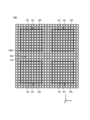
- FIG. 1 is a schematic plan view showing an outline of the configuration of a radio wave reflector according to one embodiment of the present invention
- 1 is a schematic cross-sectional view showing the configuration of a reflective antenna cell of a radio wave reflector according to one embodiment of the present invention and the direction in which radio waves are reflected by the reflective antenna cell.
- FIG. 2 is a schematic plan view showing the configuration of a patch electrode and a ground electrode of a radio wave reflector according to one embodiment of the present invention.
- FIG. 2 is a schematic plan view showing an electrode pattern of a patch electrode of a radio wave reflector according to one embodiment of the present invention.
- FIG. 2 is a schematic plan view showing an electrode pattern of a ground electrode of a radio wave reflector according to one embodiment of the present invention.
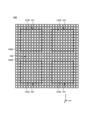
- FIG. 2 is a schematic plan view showing the configuration of a patch electrode and a ground electrode of a radio wave reflector according to one embodiment of the present invention.
- FIG. 2 is a schematic plan view showing an electrode pattern of a ground electrode of a radio wave reflector according to one embodiment of the present invention.
- FIG. 2 is a schematic plan view showing the configuration of a patch electrode and a ground electrode of a radio wave reflector according to one embodiment of the present invention.
- FIG. 2 is a schematic plan view showing an electrode pattern of a ground electrode of a radio wave reflector according to one embodiment of the present invention.
- FIG. 2 is a schematic plan view showing the configuration of a patch electrode and a ground electrode of a radio wave reflector according to one embodiment of the present invention.
- Each of the first reflecting antenna cell 100-1 and the second reflecting antenna cell 100-2 includes a patch electrode 120 provided on the first substrate 110-1 and a ground electrode 130 provided on the second substrate 110-2.
- the patch electrode 120 of the first reflecting antenna cell 100-1 and the patch electrode 120 of the second reflecting antenna cell 100-2 are not electrically connected.
- the ground electrode 130 is provided in common to the first reflecting antenna cell 100-1 and the second reflecting antenna cell 100-2.
- a first alignment film 140-1 is provided on the patch electrode 120.
- a second alignment film 140-2 is provided on the ground electrode 130.
- the first substrate 110-1 and the second substrate 110-2 are arranged so that the patch electrode 120 and the ground electrode 130 face each other, and a liquid crystal layer 150 is provided between the first alignment film 140-1 and the second alignment film 140-2.
- the first substrate 110-1 and the second substrate 110-2 can each be made of glass, quartz, resin, or the like.
- a metallic material can be used for each of the patch electrode 120 and the ground electrode 130.
- the metallic material is molybdenum (Mo), tungsten (W), titanium (Ti), aluminum (Al), copper (Cu), or an alloy of these.
- Mo molybdenum
- tungsten W
- Ti titanium
- Al aluminum
- Cu copper
- Each of the patch electrode 120 and the ground electrode 130 may have a single-layer structure or a multilayer structure.
- the first alignment film 140-1 and the second alignment film 140-2 can each be made of a polyimide resin or the like.
- the first alignment film 140-1 and the second alignment film 140-2 have been subjected to an alignment process using a rubbing method, a photoalignment method, or the like.
- the liquid crystal layer 150 contains a liquid crystal material having dielectric anisotropy.
- the liquid crystal material of the liquid crystal layer 150 may be a nematic liquid crystal or a cholesteric liquid crystal that contains liquid crystal molecules capable of twisted alignment.
- the liquid crystal layer 150 preferably contains a chiral agent to stabilize the twisted alignment of the liquid crystal molecules.
- the initial alignment state (alignment state when no voltage is applied) of the liquid crystal molecules in the liquid crystal layer 150 is controlled by the first alignment film 140-1 and the second alignment film 140-2, which have been subjected to an alignment treatment.
- the alignment state of the liquid crystal molecules in the liquid crystal layer 150 changes, and the dielectric constant of the liquid crystal layer 150 also changes. Details will be described later, but the radio wave reflector 10 uses the change in the dielectric constant of the liquid crystal layer 150 to control the phase of the reflected radio waves.
- the dielectric constant of the liquid crystal is greater when a voltage is applied than when no voltage is applied. Also, when liquid crystal molecules have negative dielectric anisotropy, the dielectric constant of the liquid crystal is smaller when a voltage is applied than when no voltage is applied.
- the liquid crystal layer 150 formed of liquid crystals having dielectric anisotropy can also be considered as a variable dielectric layer. By utilizing the dielectric anisotropy of the liquid crystal layer 150, the reflective antenna cell 100 can control the phase delay (or not delay) of radio waves scattered by the ground electrode 130.
- each of the multiple reflecting antenna cells 100 has the basic configuration described above.
- each of the multiple reflecting antenna cells 100 is electrically connected to a switching element 160.
- the switching element 160 is electrically connected to the patch electrode 120, and the voltage applied to the patch electrode 120 changes by controlling the switching element 160.
- radio waves are incident on the radio wave reflector 10 parallel to the normal direction of the surface of the first substrate 110-1 (see "Propagation direction of incident wave" in FIG. 2).
- a first voltage V1 is applied to the patch electrode 120 of the first reflecting antenna cell 100-1
- a second voltage V2 different from the first voltage V1 is applied to the patch electrode 120 of the second reflecting antenna cell 100-2.
- radio waves having the same phase are incident on the first reflecting antenna cell 100-1 and the second reflecting antenna cell 100-2
- scattered waves with different phases are generated in the first reflecting antenna cell 100-1 and the second reflecting antenna cell 100-2 because the dielectric constants of the liquid crystal layer 150 are different between the first reflecting antenna cell 100-1 and the second reflecting antenna cell 100-2.
- the phase of the scattered wave R2 scattered by the second reflecting antenna cell 100-2 leads the phase of the scattered wave R1 scattered by the first reflecting antenna cell 100-1.
- the radio wave reflected by the reflecting antenna area 11 travels in a direction different from the normal direction of the surface of the first substrate 110-1 (see "Propagation direction of reflected wave" in FIG. 2).
- FIG. 2 shows two adjacent reflecting antenna cells 100, the radio wave reflector 10 can separately control multiple reflecting antenna cells 100 arranged in a matrix. Therefore, the radio wave reflector 10 can control the reflection direction of the radio wave to any direction.
- the frequency bands to which the radio wave reflector 10 is applicable are the very high frequency (VHF) band, the ultra high frequency (UHF) band, the super high frequency (SHF) band, the submillimeter wave (THF: tremendous high frequency) band, and the millimeter wave (EHF: extra high frequency) band.
- VHF very high frequency
- UHF ultra high frequency
- SHF super high frequency
- THF submillimeter wave
- EHF millimeter wave
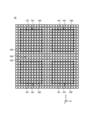
- Fig. 3 is a schematic plan view showing the configuration of the patch electrode 120 and the ground electrode 130 of the radio wave reflector 10 according to one embodiment of the present invention. Specifically, Fig. 3 is a partial enlarged view of an area A including four reflecting antenna cells 100 in Fig. 1.
- Fig. 4A is a schematic plan view showing the electrode pattern of the patch electrode 120 of the radio wave reflector 10 according to one embodiment of the present invention
- Fig. 4B is a schematic plan view showing the electrode pattern of the ground electrode 130 of the radio wave reflector 10 according to one embodiment of the present invention.
- the plan views of Fig. 4A and Fig. 4B correspond to the plan view of Fig. 3.
- the radio wave reflector 10 includes a first region 101 and a second region 102.
- the first region 101 is a region where the patch electrode 120 and the ground electrode 130 overlap in a planar view. In other words, the first region 101 is a region that corresponds to the reflecting antenna cell 100.
- the second region 102 is a region where the patch electrode 120 and the ground electrode 130 do not overlap in a planar view. In other words, the second region 102 is a region where only the ground electrode 130 is provided.
- the patch electrode 120 includes a plurality of first openings 121 having a first opening area (see FIG. 4A).
- the ground electrode 130 includes a plurality of second openings 131 having a second opening area (see FIG. 4B).
- the cross-sectional shape of each of the first openings 121 and the second openings 131 is rectangular, but is not limited to this.
- the second opening area is larger than the first opening area.
- the first openings 121 and the second openings 131 overlap. Specifically, one of the plurality of second openings 131 overlaps with four of the plurality of first openings 121.
- the ground electrode 130 includes a plurality of third openings 132 having a third opening area (see FIG. 4B).
- the cross-sectional shape of the third openings is rectangular, but is not limited to this.
- the third opening area is the same as the first opening area. In other words, the opening ratio of the ground electrode 130 in the second region 102 is smaller than the opening ratio of the ground electrode 130 in the first region 101.
- the patch electrode 120 and the ground electrode 130 do not transmit light.
- many openings are provided in the patch electrode 120 and the ground electrode 130 to allow light to pass through, and light incident on the radio wave reflector 10 passes through the openings. Therefore, the radio wave reflector 10 is a transparent radio wave reflector.
- the switching element 160 includes a semiconductor layer 161, a gate insulating layer 162, and a gate electrode 163.
- the semiconductor layer 161 is provided on the first substrate 110-1.
- the gate insulating layer 162 is provided on the first substrate 110-1 so as to cover the semiconductor layer 161.
- the gate electrode 163 is provided on the gate insulating layer 162 so as to overlap with the semiconductor layer 161.
- the gate electrode 163 is electrically connected to the selection signal line 166.
- An interlayer insulating layer 164 is provided on the gate electrode 163.
- the interlayer insulating layer 164 has two openings formed therein through which the semiconductor layer 161 is exposed.
- the semiconductor layer 161 is electrically connected to the patch electrode 120 through one opening, and is electrically connected to the data signal line 167 through the other opening.
- a planarization layer 165 is provided on the interlayer insulating layer 164 and the data signal line 167.
- the patch electrode 120 is provided on the planarization layer 165.
- the semiconductor layer 161 is formed using a silicon semiconductor such as amorphous silicon or polycrystalline silicon, or an oxide semiconductor such as indium gallium zinc oxide, indium gallium aluminum oxide, indium gallium oxide, zinc oxide, or gallium oxide.
- the gate insulating layer 162 and the interlayer insulating layer 164 are formed using, for example, a silicon oxide film or a laminated structure of a silicon oxide film and a silicon nitride film.
- the gate electrode 163 and the selection signal line 166 may be formed in the same layer.
- the gate electrode 163 and the selection signal line 166 are formed using, for example, molybdenum (Mo), tungsten (W), or an alloy thereof.
- the data signal line 167 is formed using a metal material such as titanium (Ti), aluminum (Al), or molybdenum (Mo).
- the data signal line 167 is configured with a laminated structure of titanium (Ti)/aluminum (Al)/titanium (Ti), or a laminated structure of molybdenum (Mo)/aluminum (Al)/molybdenum (Mo).
- the planarization layer 165 is formed using a resin material such as acrylic or polyimide.
- the selection signal line 166 and the data signal line 167 are electrically connected to the drive circuit of the drive circuit region 12.
- a control signal from the drive circuit is input to the switching element 160 via the selection signal line 166 and the data signal line 167.
- the switching element 160 operates based on the control signal, which changes the alignment state of the liquid crystal molecules in the liquid crystal layer 150.
- the transparency of the radio wave reflector 10 is related to the light transmittance in the radio wave reflector 10. For example, when the amount of light passing through the radio wave reflector 10 increases, the transparency of the radio wave reflector 10 improves.
- the light incident on the radio wave reflector 10 is mainly blocked by the patch electrode 120 and the ground electrode 130. Only the ground electrode 130 is provided in the second region 102.
- the patch electrode 120 and the ground electrode 130 are provided in the first region 101. Therefore, the light incident on the radio wave reflector 10 is more likely to be blocked in the first region 101 than in the second region 102. Therefore, generally, the transparency of the first region 101 is lower than that of the second region 102.
- the second opening area of the second opening 131 is large, and the light is less likely to be blocked by the ground electrode 130. Furthermore, light is incident on the radio wave reflector 10 from all directions, not just the normal direction of the first substrate 110-1 or the second substrate 110-2. However, if the second opening area of the second opening 131 is large, the light incident from all directions is more likely to pass through the first region 101. As a result, the difference between the transparency of the first region 101 and the transparency of the second region 102 is reduced, and the in-plane variation in transparency of the radio wave reflector 10 can be reduced.
- the second opening area of the second opening 131 provided in the ground electrode 130 is larger than the first opening area of the first opening 121 provided in the patch electrode 120. Therefore, the light blocking by the ground electrode 130 is reduced, and the amount of light transmitted through the first region 101 is increased. As a result, the transparency of the first region 101 is improved.
- the first opening 121 in the first region 101 and the third opening 132 in the second region 102 have the same shape and size. Therefore, the brightness of the light transmitted through the first region 101 is approximately the same as the brightness of the light transmitted through the second region 102, and the in-plane variation in the transparency of the radio wave reflector 10 can be reduced.
- a radio wave reflector 10A will be described as a first modified example of the radio wave reflector 10.
- the radio wave reflector 10A includes the same components as the radio wave reflector 10, the description of those components may be omitted.
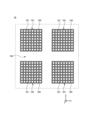
- FIG. 7 is a schematic plan view showing the configuration of the patch electrode 120A and the ground electrode 130A of the radio wave reflector 10A according to one embodiment of the present invention.
- FIG. 7 is a plan view corresponding to region A in FIG. 1.
- FIG. 8A is a schematic plan view showing the electrode pattern of the patch electrode 120A of the radio wave reflector 10A according to one embodiment of the present invention
- FIG. 8B is a schematic plan view showing the electrode pattern of the ground electrode 130A of the radio wave reflector 10A according to one embodiment of the present invention.
- the plan views of FIG. 8A and FIG. 8B correspond to the plan view of FIG. 7.
- the radio wave reflector 10A includes a first region 101 where the patch electrode 120A and the ground electrode 130A overlap, and a second region 102 where the patch electrode 120A and the ground electrode 130A do not overlap.
- the patch electrode 120A includes a plurality of first openings 121A having a first opening area (see FIG. 8A).
- the ground electrode 130A includes a plurality of second openings 131 having a second opening area (see FIG. 8B).
- the cross-sectional shape of the first opening 121A is circular, and the cross-sectional shape of the second opening 131 is rectangular.
- the second opening area is larger than the first opening area. In this way, the first opening 121A and the second opening 131 have different shapes and sizes, but in the first region 101, the first opening 121A and the second opening 131 overlap.
- one of the plurality of second openings 131 overlaps with four of the plurality of first openings 121A.
- the first region 101 is translucent because light passing through the first opening 121A and the second opening 131 is not blocked by the patch electrode 120A and the ground electrode 130A.
- the ground electrode 130A includes a plurality of third openings 132A having a third opening area (see FIG. 8B).
- the second region 102 is translucent because light passing through the third openings 132A is not blocked by the patch electrode 120A and the ground electrode 130A.
- the cross-sectional shape of the third openings 132A is rectangular.
- the third opening area is the same as the first opening area. That is, the third openings 132A have the same shape and size as the first openings 121A.
- the first opening 121A provided in the patch electrode 120A and the second opening 131 provided in the ground electrode have different shapes and sizes.
- the second opening area of the second opening 131 is larger than the first opening area of the first opening 121A, the light blocking by the ground electrode 130A is reduced and the amount of light transmitted through the first region 101 is increased.
- the transparency of the first region 101 is improved.
- the first opening 121A of the first region 101 and the third opening 132A of the second region 102 have the same shape and size. Therefore, the brightness of the light transmitted through the first region 101 is approximately the same as the brightness of the light transmitted through the second region 102, and the in-plane variation in the transparency of the radio wave reflector 10A can be reduced.
- a radio wave reflector 10B will be described as a second modified example of the radio wave reflector 10.
- the description of the components may be omitted.
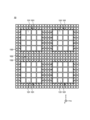
- FIG. 9 is a schematic plan view showing the configuration of the patch electrode 120 and the ground electrode 130B of a radio wave reflector 10B according to one embodiment of the present invention.
- FIG. 9 is a plan view corresponding to region A in FIG. 1.
- FIG. 10 is a schematic plan view showing the electrode pattern of the ground electrode 130B of a radio wave reflector 10B according to one embodiment of the present invention.
- the plan view of FIG. 10 corresponds to the plan view of FIG. 9.
- the electrode pattern of the patch electrode 120 of the radio wave reflector 10B is the same as the electrode pattern shown in FIG. 4A.
- the radio wave reflector 10B includes a first region 101 where the patch electrode 120 and the ground electrode 130B overlap, and a second region 102 where the patch electrode 120 and the ground electrode 130B do not overlap.
- the ground electrode 130B includes a plurality of second openings 131B having a second opening area (see FIG. 10).
- the cross-sectional shape of the first opening 121 is rectangular, and the cross-sectional shape of the second opening 131B is triangular.
- the distance between two adjacent second openings 131B i.e., the line width of the ground electrode 130B located between two adjacent second openings 131B
- the second opening area is larger than the first opening area.
- the first opening 121 and the second opening 131B have different shapes and sizes, but in the first region 101, the first opening 121 and the second opening 131B overlap each other. Specifically, one of the multiple second openings 131B overlaps with two of the multiple first openings 121. In this way, one of the multiple second openings 131B can overlap any number of the multiple first openings 121. However, if there are too many first openings 121 overlapping one of the multiple second openings 131B, it becomes difficult to generate a potential difference between the patch electrode 120 and the ground electrode 130, and the orientation of the liquid crystal molecules may not change even when a voltage is applied to the patch electrode 120. In this case, the reflection loss of the radio wave reflector 10B increases. Therefore, in order to suppress the increase in the reflection loss of the radio wave reflector 10B, it is preferable that one of the multiple second openings 131B overlaps with two to four of the multiple first openings 121.
- one of the multiple second openings 131B can overlap any number of the multiple first openings 121.
- the second opening area of the second opening 131B is larger than the first opening area of the first opening 121, so that the light blocking by the ground electrode 130 is reduced and the amount of light transmitted through the first region 101 of the radio wave reflector 10B is increased.
- the transparency of the first region 101 is improved.
- the first opening 121 of the first region 101 and the third opening 132 of the second region 102 have the same shape and size. Therefore, the brightness of the light transmitted through the first region 101 is approximately the same as the brightness of the light transmitted through the second region 102, and the in-plane variation in the transparency of the radio wave reflector 10B can be reduced.
- a radio wave reflector 10C will be described as a third modified example of the radio wave reflector 10.
- the description of the components may be omitted.
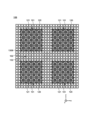
- FIG. 11 is a schematic plan view showing the configuration of the patch electrode 120 and ground electrode 130C of a radio wave reflector 10C according to one embodiment of the present invention.
- FIG. 12 is a plan view corresponding to region A in FIG. 1.
- FIG. 12 is also a schematic plan view showing the electrode pattern of the ground electrode 130C of a radio wave reflector 10C according to one embodiment of the present invention.
- the plan view of FIG. 12 corresponds to the plan view of FIG. 11.
- the electrode pattern of the patch electrode 120 of the radio wave reflector 10C is the same as the electrode pattern shown in FIG. 4A.
- the radio wave reflector 10C includes a first region 101 where the patch electrode 120 and the ground electrode 130C overlap, and a second region 102 where the patch electrode 120 and the ground electrode 130C do not overlap.
- the ground electrode 130C includes a plurality of second openings 131C having a second opening area (see FIG. 12).
- the cross-sectional shape of each of the plurality of second openings 131C is polygonal.
- the sizes of the plurality of second openings 131C are not the same. That is, the second opening area of the plurality of second openings 131C increases from the inside to the outside of the first region 101.
- the second opening area of the second opening 131C located on the innermost side of the first region 101 is the same as the first opening area of the first opening 121.
- it is preferable that the second opening area of the second opening 131 located on the innermost side of the first region 101 is larger than the first opening area of the first opening 121.
- the electrode pattern of the ground electrode 130C in the first region 101 completely overlaps with the electrode pattern of the patch electrode 120 in the first region 101, but it is also possible to configure the electrode pattern of the ground electrode 130C in the first region 101 to overlap with a shifted electrode pattern of the patch electrode 120 in the first region 101.
- the first opening area of the first opening 121D provided in the patch electrode 120D is larger than the second opening area of the second opening 131D provided in the ground electrode 130D. Therefore, the light blocking by the patch electrode is reduced, and the amount of light transmitted through the first region 101 is increased. As a result, the transparency of the first region 101 is improved.
- the second opening 131D of the first region 101 and the third opening 132D of the second region 102 have the same shape and size. Therefore, the brightness of the light transmitted through the first region 101 is approximately the same as the brightness of the light transmitted through the second region 102, and the in-plane variation in the transparency of the radio wave reflector 10D can be reduced.
- the opening area of the third openings 132 is made smaller, and the brightness of the light passing through the second region 102 is adjusted to match the brightness of the light passing through the first region 101.
- the difference in transparency between the first region 101 and the second region 102 becomes smaller, and the in-plane variation in transparency of the radio wave reflector 10E can be reduced.
- 10, 10A, 10B, 10C, 10D, 10E radio wave reflector, 11: reflecting antenna area, 12: driving circuit area, 100: reflecting antenna cell, 100-1: first reflecting antenna cell, 100-2: second reflecting antenna cell, 101: first area, 102: second area, 110-1: first substrate, 110-2: second substrate, 120, 120A, 120D: patch electrode, 121, 121A, 121D: first opening, 130, 130A, 130B, 130C, 130D, 130E: ground electrode, 131, 131B, 131C, 131D, 131E: second opening, 132, 132A, 132D, 132E: third opening, 140-1: first alignment film, 140-2: second alignment film, 150: liquid crystal layer, 160: switching element, 161: semiconductor layer, 162: gate insulating layer, 163: gate electrode, 164: interlayer insulating layer, 165: planarization layer, 166: selection signal line, 167: data signal line
Landscapes
- Physics & Mathematics (AREA)
- Electromagnetism (AREA)
- Aerials With Secondary Devices (AREA)
Abstract
電波反射板は、第1の基板の上のパッチ電極と、第1の基板と異なる第2の基板の上の接地電極と、パッチ電極と接地電極との間の液晶層と、平面視において、接地電極がパッチ電極と重畳する第1の領域および接地電極がパッチ電極と重畳しない第2の領域と、を含み、第1の領域において、パッチ電極は第1の開口面積を有する複数の第1の開口部を含み、かつ、接地電極は第2の開口面積を有する複数の第2の開口部を含み、第2の領域において、接地電極は第3の開口面積を有する複数の第3の開口部を含み、複数の第2の開口部は、複数の第1の開口部と重畳し、第2の開口面積は、第1の開口面積よりも大きい。
Description
本発明の一実施形態は、入射する電波の反射方向を制御することのできる電波反射板に関する。
フェーズドアレイアンテナ(Phased Array Antenna)装置(以下、「電波反射板」という場合がある。)は、面状に配列された複数のアンテナ素子のそれぞれに対し、印加する高周波信号の振幅と位相を調整することでアンテナを固定した状態で指向性を制御している。フェーズドアレイアンテナ装置は移相器を必要とする。液晶の配向状態による誘電率の変化を利用した移相器を用いたフェーズドアレイアンテナ装置が開示されている(例えば、特許文献1参照)。
特許文献1におけるフェーズドアレイアンテナ装置のアンテナ素子は、複数のストリップ配線と、複数のストリップ配線と対向する平面電極と、複数のストリップ配線と平面電極との間に設けられた液晶層と、を有する。複数のアンテナ素子において、複数のストリップ配線に異なる電圧を印加する。そして、アンテナ素子ごとの液晶層の誘電率を調整して、反射波を重ね合わせることで、位相を変化させることができる。これにより、電波の反射方向を任意の方向に設定することができる。
電波反射板は電波基地局を簡素化することができる。但し、電波反射板の設置によって景観が損なわれるという問題があるため、第5世代移動通信システム(G5)用の電波反射板として、透明な電波反射板が要望されている。液晶を用いた電波反射板では、透明化が可能である。しかしながら、液晶を用いた透明な電波反射板であっても、電波反射板に含まれる電極の形状が視認されるなど、面内における透明度のばらつきが問題となっている。そのため、透明な電波反射板の透明度の面内ばらつきの改善が望まれている。
本発明の一実施形態は、上記問題に鑑み、透明度の面内ばらつきが抑制された透明な電波反射板を提供することを目的の一つとする。
本発明の一実施形態に係る電波反射板は、第1の基板の上のパッチ電極と、第1の基板と異なる第2の基板の上の接地電極と、パッチ電極と接地電極との間の液晶層と、平面視において、接地電極がパッチ電極と重畳する第1の領域および接地電極がパッチ電極と重畳しない第2の領域と、を含み、第1の領域において、パッチ電極は第1の開口面積を有する複数の第1の開口部を含み、かつ、接地電極は第2の開口面積を有する複数の第2の開口部を含み、第2の領域において、接地電極は第3の開口面積を有する複数の第3の開口部を含み、複数の第2の開口部は、複数の第1の開口部と重畳し、第2の開口面積は、第1の開口面積よりも大きい。
以下、本発明の実施形態を、図面などを参照しながら説明する。但し、本発明は多くの異なる態様で実施することが可能であり、以下に例示する実施形態の記載内容に限定して解釈されるものではない。図面は説明をより明確にするため、実際の態様に比べ、各部の幅、厚さ、形状などについて模式的に表される場合があるが、あくまで一例であって、本発明の解釈を限定するものではない。また、本明細書と図面において、既出の図に関して前述したものと同様の構成要素には、同一の符号を付して、詳細な説明を適宜省略する場合がある。さらに、構成要素に「第1」、「第2」と付記された文字は、構成要素を区別するために用いられる便宜的な標識であり、特段の説明がない限りそれ以上の意味を有しない。
本明細書において、ある部材または領域が他の部材または領域の「上に(または下に)」あるとする場合、特段の限定がない限りこれは他の部材または領域の直上(または直下)にある場合のみでなく他の部材または領域の上方(または下方)にある場合を含み、すなわち、他の部材または領域の上方(または下方)において間に別の構成要素が含まれている場合も含む。
図1~図6を参照して、本発明の一実施形態に係る電波反射板10について説明する。
[1.電波反射板10の構成]
図1は、本発明の一実施形態に係る電波反射板10の構成の概要を示す模式的な平面図である。
図1は、本発明の一実施形態に係る電波反射板10の構成の概要を示す模式的な平面図である。
図1に示すように、電波反射板10は、反射アンテナ領域11および駆動回路領域12を含む。反射アンテナ領域11は、電波反射板10の中央部に設けられ、駆動回路領域12は、電波反射板10の周辺部に設けられている。換言すると、駆動回路領域12は、反射アンテナ領域11の周囲に設けられている。反射アンテナ領域11には、複数の反射アンテナセル100が設けられている。複数の反射アンテナセル100は、x軸方向およびy軸方向にマトリックス状に配置されている。但し、複数の反射アンテナセル100の配置構成は、この限りではない。駆動回路領域12には、複数の反射アンテナセル100の各々を制御する制御信号を生成する駆動回路が設けられている。なお、図示しないが、電波反射板10の周辺部には、外部から信号または電力を供給するための端子部が設けられてもよい。
ここで、図2を参照して、反射アンテナセル100の構成および機能について説明する。
図2は、本発明の一実施形態に係る電波反射板10の反射アンテナセル100の構成および反射アンテナセル100による電波の反射方向を示す模式的な断面図である。図2には、隣接する2つの反射アンテナセル100として、第1の反射アンテナセル100-1および第2の反射アンテナセル100-2が示されている。
第1の反射アンテナセル100-1および第2の反射アンテナセル100-2の各々は、第1の基板110-1の上に設けられたパッチ電極120および第2の基板110-2の上に設けられた接地電極130を含む。第1の反射アンテナセル100-1のパッチ電極120と第2の反射アンテナセル100-2のパッチ電極120とは、電気的に接続されていない。一方、接地電極130は、第1の反射アンテナセル100-1および第2の反射アンテナセル100-2に共通して設けられている。パッチ電極120の上には、第1の配向膜140-1が設けられている。接地電極130の上には、第2の配向膜140-2が設けられている。第1の基板110-1と第2の基板110-2とは、パッチ電極120と接地電極130とが対向するように配置され、第1の配向膜140-1と第2の配向膜140-2との間には液晶層150が設けられている。
第1の基板110-1および第2の基板110-2の各々として、ガラス、石英、または樹脂などを用いることができる。
パッチ電極120および接地電極130の各々として、金属材料を用いることができる。例えば、金属材料は、モリブデン(Mo)、タングステン(W)、チタン(Ti)、アルミニウム(Al)、もしくは銅(Cu)またはこれらの合金である。なお、パッチ電極120および接地電極130の各々は、単層構造を有していてもよく、積層構造を有していてもよい。
第1の配向膜140-1および第2の配向膜140-2の各々として、ポリイミド樹脂などを用いることができる。第1の配向膜140-1および第2の配向膜140-2には、ラビング法または光配向法などを用いて配向処理が行われている。
液晶層150は、誘電異方性を有する液晶材料を含む。例えば、液晶層150の液晶材料として、ツイスト配向が可能な液晶分子を含むネマチック液晶またはコレステリック液晶などを用いることができる。また、液晶層150は、液晶分子のツイスト配向を安定化させるため、カイラル剤が含まれていることが好ましい。
配向処理が行われた第1の配向膜140-1および第2の配向膜140-2により、液晶層150内の液晶分子は、初期配向状態(電圧無印加時の配向状態)が制御されている。パッチ電極120に電圧が印加され、パッチ電極120と接地電極130との間に電位差が形成されると、液晶層150内の液晶分子の配向状態が変化し、液晶層150の誘電率も変化する。詳細は後述するが、電波反射板10では、液晶層150の誘電率の変化を利用し、反射する電波の位相を制御する。
液晶分子が正の誘電異方性を有する場合、電圧無印加時よりも電圧印加時の方が、液晶の誘電率が大きくなる。また、液晶分子が負の誘電異方性を有する場合、電圧無印加時よりも電圧印加時の方が、液晶の誘電率が小さくなる。誘電異方性を有する液晶で形成された液晶層150は可変誘電体層とみなすこともできる。反射アンテナセル100は、液晶層150の誘電異方性を利用することで、接地電極130で散乱する電波の位相を遅らせる(または遅らせない)ように制御することができる。
上述したように、第1の反射アンテナセル100-1および第2の反射アンテナセル100-2における基本的な構成は同じである。すなわち、複数の反射アンテナセル100の各々は、上述した基本的な構成を有する。一方、複数の反射アンテナセル100の各々は、スイッチング素子160と電気的に接続されている。具体的には、スイッチング素子160は、パッチ電極120と電気的に接続されており、スイッチング素子160を制御することにより、パッチ電極120に印加される電圧が変化する。
図2に示すように、電波は、第1の基板110-1の表面の法線方向と平行に電波反射板10に入射される(図2中の「入射波の進行方向」参照)。ここで、第1の反射アンテナセル100-1のパッチ電極120には第1の電圧V1が印加され、第2の反射アンテナセル100-2のパッチ電極120には第1の電圧V1と異なる第2の電圧V2が印加されている場合を考える。第1の反射アンテナセル100-1および第2の反射アンテナセル100-2に同じ位相を有する電波が入射すると、第1の反射アンテナセル100-1と第2の反射アンテナセル100-2とでは液晶層150の誘電率が異なることから、第1の反射アンテナセル100-1と第2の反射アンテナセル100-2とにおいて、位相の異なる散乱波が生成される。例えば、図2に示すように、第2の反射アンテナセル100-2で散乱する散乱波R2の位相は、第1の反射アンテナセル100-1で散乱する散乱波R1の位相よりも進む。この場合、反射アンテナ領域11で反射される電波は、第1の基板110-1の表面の法線方向とは異なる方向に進行する(図2中の「反射波の進行方向」参照)。図2には、隣接する2つの反射アンテナセル100を示したが、電波反射板10では、マトリクス状に配置された複数の反射アンテナセル100を別個に制御することができる。そのため、電波反射板10は、電波の反射方向を任意の方向に制御することができる。
電波反射板10の適用対象とする周波数帯は、超短波(VHF:Very High Frequency)帯、極超短波(UHF:Ultra-High Frequency)帯、マイクロ波(SHF:Super High Frequency)帯、サブミリ波(THF:Tremendously high frequency)、ミリ波(EHF:Extra High Frequency)帯である。上述したように、液晶層150では、パッチ電極120に印加される電圧によって液晶分子の配向状態が変化するが、接地電極130に入射する電波の周波数にはほとんど追従しない。液晶分子のこのような特性により、パッチ電極120によって液晶層150の誘電率を変化させつつ、接地電極130で電波を散乱させ、散乱される電波の位相を制御することができる。
[2.パッチ電極120および接地電極130の構成]
図3は、本発明の一実施形態に係る電波反射板10のパッチ電極120および接地電極130の構成を示す模式的な平面図である。具体的には、図3は、図1における4つの反射アンテナセル100を含む領域Aの部分拡大図である。また、図4Aは、本発明の一実施形態に係る電波反射板10のパッチ電極120の電極パターンを示す模式的な平面図であり、図4Bは、本発明の一実施形態に係る電波反射板10の接地電極130の電極パターンを示す模式的な平面図である。図4Aおよび図4Bの平面図は、図3の平面図と対応している。
図3は、本発明の一実施形態に係る電波反射板10のパッチ電極120および接地電極130の構成を示す模式的な平面図である。具体的には、図3は、図1における4つの反射アンテナセル100を含む領域Aの部分拡大図である。また、図4Aは、本発明の一実施形態に係る電波反射板10のパッチ電極120の電極パターンを示す模式的な平面図であり、図4Bは、本発明の一実施形態に係る電波反射板10の接地電極130の電極パターンを示す模式的な平面図である。図4Aおよび図4Bの平面図は、図3の平面図と対応している。
電波反射板10は、第1の領域101および第2の領域102を含む。第1の領域101は、平面視において、パッチ電極120と接地電極130とが重畳する領域である。すなわち、第1の領域101は、反射アンテナセル100に相当する領域である。第2の領域102は、平面視において、パッチ電極120と接地電極130とが重畳しない領域である。すなわち、第2の領域102は、接地電極130のみが設けられた領域である。
第1の領域101において、パッチ電極120は、第1の開口面積を有する複数の第1の開口部121を含む(図4A参照)。また、第1の領域101において、接地電極130は、第2の開口面積を有する複数の第2の開口部131を含む(図4B参照)。第1の開口部121および第2の開口部131の各々の断面形状は矩形であるが、これに限られない。第2の開口面積は、第1の開口面積よりも大きい。また、第1の開口部121と第2の開口部131とは重畳している。具体的には、複数の第2の開口部131の1個が、複数の第1の開口部121の4個と重畳している。
第2の領域102において、接地電極130は、第3の開口面積を有する複数の第3の開口部132を含む(図4B参照)。第3の開口部の断面形状は矩形であるが、これに限られない。第3の開口面積は、第1の開口面積と同じである。換言すると、第2の領域102における接地電極130の開口率は、第1の領域101における接地電極130の開口率よりも小さい。
パッチ電極120および接地電極130は、光を透過しない。しかしながら、電波反射板10では、光を透過させるために、パッチ電極120および接地電極130に多くの開口部(複数の第1の開口部121、複数の第2の開口部131、および複数の第3の開口部132)が設けられており、電波反射板10に入射した光は、開口部を透過する。そのため、電波反射板10は、透明な電波反射板となる。
ここで、図5および図6を参照して、透明な電波反射板である電波反射板10の第1の領域101におけるパッチ電極120および接地電極130の構成についてさらに詳細に説明する。
図5は、本発明の一実施形態に係る電波反射板10の第1の領域101の構成を示す模式的な平面図である。図6は、本発明の一実施形態に係る電波反射板10の第1の領域101の構成を示す模式的な断面図である。具体的には、図6は、図5中のB1-B2線で切断された第1の領域101の断面図である。上述したように、第1の領域101は、反射アンテナセル100に相当する。
図5および図6には、スイッチング素子160の一例として、トランジスタが示されている。すなわち、スイッチング素子160は、半導体層161、ゲート絶縁層162、およびゲート電極163を含む。半導体層161は、第1の基板110-1の上に設けられている。ゲート絶縁層162は、半導体層161を覆うように、第1の基板110-1の上に設けられている。ゲート電極163は、半導体層161と重畳するように、ゲート絶縁層162の上に設けられている。ゲート電極163は、選択信号線166と電気的に接続されている。ゲート電極163の上には、層間絶縁層164が設けられている。層間絶縁層164には、半導体層161が露出される2つの開口が形成されている。半導体層161は、一方の開口を介してパッチ電極120と電気的に接続され、他方の開口を介してデータ信号線167と電気的に接続されている。層間絶縁層164およびデータ信号線167の上には、平坦化層165が設けられている。パッチ電極120は、平坦化層165の上に設けられている。
半導体層161は、アモルファスシリコンもしくは多結晶シリコンなどのシリコン半導体、または酸化インジウムガリウム亜鉛、酸化インジウムガリウムアルミニウム、酸化インジウムガリウム、酸化亜鉛、もしくは酸化ガリウムなどの酸化物半導体を用いて形成される。ゲート絶縁層162および層間絶縁層164は、例えば、酸化シリコン膜、または酸化シリコン膜と窒化シリコン膜との積層構造を用いて形成される。ゲート電極163と選択信号線166とは、同一層で形成されていてもよい。ゲート電極163および選択信号線166は、例えば、モリブデン(Mo)、タングステン(W)、またはこれらの合金を用いて形成される。データ信号線167は、チタン(Ti)、アルミニウム(Al)、またはモリブデン(Mo)などの金属材料を用いて形成される。例えば、データ信号線167は、チタン(Ti)/アルミニウム(Al)/チタン(Ti)の積層構造、またはモリブデン(Mo)/アルミニウム(Al)/モリブデン(Mo)の積層構造で構成される。平坦化層165は、アクリルまたはポリイミドなどの樹脂材料を用いて形成される。
選択信号線166およびデータ信号線167は、駆動回路領域12の駆動回路と電気的に接続されている。駆動回路からの制御信号は、選択信号線166およびデータ信号線167を介してスイッチング素子160に入力される。スイッチング素子160は、制御信号に基づいて動作し、これにより、液晶層150内の液晶分子の配向状態が変化する。
ところで、電波反射板10の透明度は、電波反射板10における光の透過性と関連する。例えば、電波反射板10を透過する光が増加すると、電波反射板10の透明度が向上する。電波反射板10に入射する光は、主に、パッチ電極120および接地電極130によって遮光される。第2の領域102には接地電極130のみが設けられている。一方、第1の領域101にはパッチ電極120および接地電極130が設けられている。そのため、電波反射板10に入射する光は、第2の領域102よりも第1の領域101において遮光されやすい。そのため、一般的には、第1の領域101は、第2の領域102よりも透明度が低下する。しかしながら、電波反射板10の第1の領域101では、第2の開口部131の第2の開口面積が大きく、接地電極130によって遮光されにくい。また、光は、第1の基板110-1または第2の基板110-2の法線方向だけでなく、あらゆる方向から電波反射板10に入射するが、第2の開口部131の第2の開口面積が大きいと、第1の領域101において、あらゆる方向から入射した光が透過しやすくなる。その結果、第1の領域101の透明度と第2の領域102の透明度との差が小さくなり、電波反射板10における透明度の面内ばらつきを低減することができる。
以上説明したように、電波反射板10の第1の領域101(反射アンテナセル100)では、接地電極130に設けられた第2の開口部131の第2の開口面積が、パッチ電極120に設けられた第1の開口部121の第1の開口面積よりも大きい。そのため、接地電極130による遮光が低減され、第1の領域101を透過する光が増加する。その結果、第1の領域101の透明度が向上する。また、第1の領域101の第1の開口部121と第2の領域102の第3の開口部132とは形状および大きさが同じである。そのため、第1の領域101を透過する光の明るさは、第2の領域102を透過する光の明るさと同程度となり、電波反射板10における透明度の面内ばらつきを低減することができる。
<変形例1>
図7~図8Bを参照して、電波反射板10の第1の変形例として電波反射板10Aについて説明する。なお、以下では、電波反射板10Aが電波反射板10と同様の構成要素を含むとき、その構成要素の説明を省略する場合がある。
図7~図8Bを参照して、電波反射板10の第1の変形例として電波反射板10Aについて説明する。なお、以下では、電波反射板10Aが電波反射板10と同様の構成要素を含むとき、その構成要素の説明を省略する場合がある。
図7は、本発明の一実施形態に係る電波反射板10Aのパッチ電極120Aおよび接地電極130Aの構成を示す模式的な平面図である。図7は、図1中の領域Aに対応する平面図である。また、図8Aは、本発明の一実施形態に係る電波反射板10Aのパッチ電極120Aの電極パターンを示す模式的な平面図であり、図8Bは、本発明の一実施形態に係る電波反射板10Aの接地電極130Aの電極パターンを示す模式的な平面図である。図8Aおよび図8Bの平面図は、図7の平面図と対応している。
平面視において、電波反射板10Aは、パッチ電極120Aと接地電極130Aとが重畳する第1の領域101およびパッチ電極120Aと接地電極130Aとが重畳しない第2の領域102を含む。
第1の領域101において、パッチ電極120Aは、第1の開口面積を有する複数の第1の開口部121Aを含む(図8A参照)。また、第1の領域101において、接地電極130Aは、第2の開口面積を有する複数の第2の開口部131を含む(図8B参照)。第1の開口部121Aの断面形状は円形であり、第2の開口部131の断面形状は矩形である。また、第2の開口面積は、第1の開口面積よりも大きい。このように、第1の開口部121Aと第2の開口部131とは形状および大きさが異なるが、第1の領域101において、第1の開口部121Aと第2の開口部131とは重畳している。具体的には、複数の第2の開口部131の1個が、複数の第1の開口部121Aの4個と重畳している。第1の開口部121Aおよび第2の開口部131を透過する光はパッチ電極120Aおよび接地電極130Aによって遮光されないため、第1の領域101は透光性を有する。
第2の領域102において、接地電極130Aは、第3の開口面積を有する複数の第3の開口部132Aを含む(図8B参照)。第3の開口部132Aを透過する光はパッチ電極120Aおよび接地電極130Aによって遮光されないため、第2の領域102は透光性を有する。第3の開口部132Aの断面形状は矩形である。第3の開口面積は、第1の開口面積と同じである。すなわち、第3の開口部132Aは、第1の開口部121Aと同様の形状および大きさを有する。
以上説明したように、電波反射板10Aの第1の領域101(反射アンテナセル100)では、パッチ電極120Aに設けられた第1の開口部121Aと接地電極に設けられた第2の開口部131とは形状および大きさが異なる。しかしながら、第2の開口部131の第2の開口面積が、第1の開口部121Aの第1の開口面積よりも大きいため、接地電極130Aによる遮光が低減され、第1の領域101を透過する光が増加する。その結果、第1の領域101の透明度が向上する。また、第1の領域101の第1の開口部121Aと第2の領域102の第3の開口部132Aとは形状および大きさが同じである。そのため、第1の領域101を透過する光の明るさは、第2の領域102を透過する光の明るさと同程度となり、電波反射板10Aにおける透明度の面内ばらつきを低減することができる。
<変形例2>
図9および図10を参照して、電波反射板10の第2の変形例として電波反射板10Bについて説明する。なお、以下では、電波反射板10Bが電波反射板10と同様の構成要素を含むとき、その構成要素の説明を省略する場合がある。
図9および図10を参照して、電波反射板10の第2の変形例として電波反射板10Bについて説明する。なお、以下では、電波反射板10Bが電波反射板10と同様の構成要素を含むとき、その構成要素の説明を省略する場合がある。
図9は、本発明の一実施形態に係る電波反射板10Bのパッチ電極120および接地電極130Bの構成を示す模式的な平面図である。図9は、図1中の領域Aに対応する平面図である。また、図10は、本発明の一実施形態に係る電波反射板10Bの接地電極130Bの電極パターンを示す模式的な平面図である。図10の平面図は、図9の平面図と対応している。なお、電波反射板10Bのパッチ電極120の電極パターンは、図4Aに示す電極パターンと同様である。
平面視において、電波反射板10Bは、パッチ電極120と接地電極130Bとが重畳する第1の領域101およびパッチ電極120と接地電極130Bとが重畳しない第2の領域102を含む。
第1の領域101において、接地電極130Bは、第2の開口面積を有する複数の第2の開口部131Bを含む(図10参照)。第1の開口部121の断面形状は矩形であり、第2の開口部131Bの断面形状は三角形である。隣接する2つの第2の開口部131B間の距離(すなわち、隣接する2つの第2の開口部131B間に位置する接地電極130Bの線幅)は、隣接する2つの第1の開口部121間の距離(すなわち、隣接する2つの第1の開口部121間に位置するパッチ電極120の線幅)よりも小さい。そのため、第2の開口面積は、第1の開口面積よりも大きい。第1の開口部121と第2の開口部131Bとは形状および大きさが異なるが、第1の領域101において、第1の開口部121と第2の開口部131Bとは重畳している。具体的には、複数の第2の開口部131Bの1個が、複数の第1の開口部121の2個と重畳している。このように、複数の第2の開口部131Bの1個は、複数の第1の開口部121のうちの任意の個数と重畳することができる。但し、複数の第2の開口部131Bの1個と重畳する第1の開口部121の個数が多すぎると、パッチ電極120と接地電極130との間で電位差が生成されにくくなり、パッチ電極120に電圧を印加しても液晶分子の配向が変化しなくなる場合がある。この場合、電波反射板10Bの反射損失が増加する。そのため、電波反射板10Bの反射損失の増加を抑制するためにも、複数の第2の開口部131Bの1個は、複数の第1の開口部121の2~4個と重畳することが好ましい。
以上説明したように、電波反射板10Bの第1の領域101(反射アンテナセル100)では、複数の第2の開口部131Bの1個が、複数の第1の開口部121のうちの任意の個数と重畳することができる。この場合であっても、第2の開口部131Bの第2の開口面積は、第1の開口部121の第1の開口面積よりも大きいため、接地電極130による遮光が低減され、電波反射板10Bの第1の領域101を透過する光が増加する。その結果、第1の領域101の透明度が向上する。また、第1の領域101の第1の開口部121と第2の領域102の第3の開口部132とは形状および大きさが同じである。そのため、第1の領域101を透過する光の明るさは、第2の領域102を透過する光の明るさと同程度となり、電波反射板10Bにおける透明度の面内ばらつきを低減することができる。
<変形例3>
図11および図12を参照して、電波反射板10の第3の変形例として電波反射板10Cについて説明する。なお、以下では、電波反射板10Cが電波反射板10と同様の構成要素を含むとき、その構成要素の説明を省略する場合がある。
図11および図12を参照して、電波反射板10の第3の変形例として電波反射板10Cについて説明する。なお、以下では、電波反射板10Cが電波反射板10と同様の構成要素を含むとき、その構成要素の説明を省略する場合がある。
図11は、本発明の一実施形態に係る電波反射板10Cのパッチ電極120および接地電極130Cの構成を示す模式的な平面図である。図12は、図1中の領域Aに対応する平面図である。また、図12は、本発明の一実施形態に係る電波反射板10Cの接地電極130Cの電極パターンを示す模式的な平面図である。図12の平面図は、図11の平面図と対応している。なお、電波反射板10Cのパッチ電極120の電極パターンは、図4Aに示す電極パターンと同様である。
平面視において、電波反射板10Cは、パッチ電極120と接地電極130Cとが重畳する第1の領域101およびパッチ電極120と接地電極130Cとが重畳しない第2の領域102を含む。
第1の領域101において、接地電極130Cは、第2の開口面積を有する複数の第2の開口部131Cを含む(図12参照)。複数の第2の開口部131Cの各々の断面形状は多角形である。しかしながら、複数の第2の開口部131Cの大きさは同じではない。すなわち、複数の第2の開口部131Cは、第1の領域101の内側から外側に向かって第2の開口面積が大きくなる。なお、第1の領域101の最も内側に位置する第2の開口部131Cの第2の開口面積は、第1の開口部121の第1の開口面積と同じである。但し、第1の領域101の中心近傍の明るさを向上させるためには、第1の領域101の最も内側に位置する第2の開口部131の第2の開口面積は、第1の開口部121の第1の開口面積よりも大きいことが好ましい。
なお、本変形例では、第1の領域101における接地電極130Cの電極パターンが、第1の領域101におけるパッチ電極120の電極パターンと完全に重畳する構成を示したが、第1の領域101における接地電極130Cの電極パターンが、第1の領域101におけるパッチ電極120の電極パターンとずれて重畳する構成も可能である。
以上説明したように、電波反射板10Cの第1の領域101(反射アンテナセル100)では、複数の第2の開口部131Cが、第1の領域101の内側から外側に向かって第2の開口面積が大きくなる。透明な電波反射板では、パッチ電極120が設けられる第1の領域101とパッチ電極120が設けられない第2の領域102との境界において、第1の領域101の形状が視認されやすい。そのため、第1の領域101を透過する光の明るさを段階的に変化させることにより、すなわち、第1の領域101の内側から外側に向かって透過する光を徐々に明るくすることにより、第1の領域101と第2の領域102との境界における透明度の違いを目立たなくさせることができる。また、第1の領域101の第1の開口部121と第2の領域102の第3の開口部132とは形状および大きさが同じである。そのため、第1の領域101を透過する光の明るさは、第2の領域102を透過する光の明るさと同程度となり、電波反射板10Bにおける透明度の面内ばらつきを低減することができる。さらに、電波反射板10Cの第1の領域101の内側では、パッチ電極120と接地電極130とが重畳する領域の面積を大きくすることができる。そのため、電波反射板10Cの反射損失の増加を抑制することができる。
<変形例4>
図13~図14Bを参照して、電波反射板10の第4の変形例として電波反射板10Dについて説明する。なお、以下では、電波反射板10Dが電波反射板10と同様の構成要素を含むとき、その構成要素の説明を省略する場合がある。
図13~図14Bを参照して、電波反射板10の第4の変形例として電波反射板10Dについて説明する。なお、以下では、電波反射板10Dが電波反射板10と同様の構成要素を含むとき、その構成要素の説明を省略する場合がある。
図13は、本発明の一実施形態に係る電波反射板10Dのパッチ電極120Dおよび接地電極130Dの構成を示す模式的な平面図である。図14は、図1中の領域Aに対応する平面図である。また、図14Aは、本発明の一実施形態に係る電波反射板10Dのパッチ電極120Dの電極パターンを示す模式的な平面図であり、図14Bは、本発明の一実施形態に係る電波反射板10Dの接地電極130Dの電極パターンを示す模式的な平面図である。図14Aおよび図14Bの平面図は、図13の平面図と対応している。
平面視において、電波反射板10Dは、パッチ電極120Dと接地電極130Dとが重畳する第1の領域101およびパッチ電極120Dと接地電極130Dとが重畳しない第2の領域102を含む。
第1の領域101において、パッチ電極120Aは、第1の開口面積を有する複数の第1の開口部121Dを含む(図14A参照)。また、第1の領域101において、接地電極130Dは、第2の開口面積を有する第2の開口部131Dを含む(図14B参照)。第1の開口部121Dおよび第2の開口部131Dの各々の断面形状は矩形であるが、これに限られない。第2の開口面積は、第1の開口面積よりも小さい。また、第1の開口部121Dと第2の開口部131Dとは重畳している。具体的には、複数の第1の開口部121Dの1個が、複数の第2の開口部131Dの4個と重畳している。
第2の領域102において、接地電極130Dは、第3の開口面積を有する複数の第3の開口部132Dを含む(図14B参照)。第3の開口部132Dの断面形状は矩形であるが、これに限られない。第3の開口面積は、第2の開口面積と同じである。そのため、第3の開口部132Dは、第2の開口部131Dと同一の構成を有する。換言すると、接地電極130Dは、第1の領域101および第2の領域102において、第2の開口面積を有する複数の第2の開口部131Dを有する。
電波反射板10Dは、電波反射板10の第1の領域101において、パッチ電極120に設けられた第1の開口部121の第1の開口面積の大きさと接地電極130に設けられた第2の開口部131の第2の開口面積の大きさとが逆である構成を有する。電波反射板10Dの第1の領域101においても、第1の開口部121Dの第1の開口面積が大きいため、パッチ電極120Dによって遮光されにくい。
以上説明したように、電波反射板10Dの第1の領域101(反射アンテナセル100)では、パッチ電極120Dに設けられた第1の開口部121Dの第1の開口面積が、接地電極130Dに設けられた第2の開口部131Dの第2の開口面積よりも大きい。そのため、パッチ電極による遮光が低減され、第1の領域101を透過する光が増加する。その結果、第1の領域101の透明度が向上する。また、第1の領域101の第2の開口部131Dと第2の領域102の第3の開口部132Dとは形状および大きさが同じである。そのため、第1の領域101を透過する光の明るさは、第2の領域102を透過する光の明るさと同程度となり、電波反射板10Dにおける透明度の面内ばらつきを低減することができる。
<変形例5>
図15および図16を参照して、電波反射板10の第5の変形例として電波反射板10Eについて説明する。なお、以下では、電波反射板10Eが電波反射板10と同様の構成要素を含むとき、その構成要素の説明を省略する場合がある。
図15および図16を参照して、電波反射板10の第5の変形例として電波反射板10Eについて説明する。なお、以下では、電波反射板10Eが電波反射板10と同様の構成要素を含むとき、その構成要素の説明を省略する場合がある。
図15は、本発明の一実施形態に係る電波反射板10Eのパッチ電極120および接地電極130Eの構成を示す模式的な平面図である。図15は、図1中の領域Aに対応する平面図である。また、図16は、本発明の一実施形態に係る電波反射板10Eの接地電極130Eの電極パターンを示す模式的な平面図である。図16の平面図は、図15の平面図と対応している。なお、電波反射板10Eのパッチ電極120の電極パターンは、図4Aに示す電極パターンと同様である。
平面視において、電波反射板10Eは、パッチ電極120と接地電極130Eとが重畳する第1の領域101およびパッチ電極120と接地電極130Eとが重畳しない第2の領域102を含む。
第1の領域101において、接地電極130Eは、第2の開口面積を有する複数の第2の開口部131Eを含む(図16参照)。第2の開口部131Eの断面形状は矩形である。第2の開口面積は、第1の開口面積よりも大きい。また、第1の開口部121と第2の開口部131Eとは重畳している。具体的には、複数の第2の開口部131Eの1個が,、複数の第1の開口部121の4個と重畳している。
第2の領域102において、接地電極130Eは、第3の開口面積を有する複数の第3の開口部132Eを含む(図16参照)。第3の開口部132Eの断面形状は矩形である。第3の開口面積は、第1の開口面積よりも小さい。第2の領域102には接地電極130Eのみが設けられている。一方、第1の領域101にはパッチ電極120および接地電極130Eが設けられている。そのため、電波反射板10Eに入射する光は、第2の領域102よりも第1の領域101において遮光されやすい。そこで、電波反射板10Eの第2の領域102では、第3の開口部132の開口面積を小さくし、第1の領域101を透過する光の明るさに合わせて第2の領域102を透過する光の明るさを調整している。その結果、第1の領域101の透明度と第2の領域102の透明度との差が小さくなり、電波反射板10Eにおける透明度の面内ばらつきを低減することができる。
以上説明したように、電波反射板10Eの第1の領域101(反射アンテナセル100)では、接地電極130Eに設けられた第2の開口部131Eの第2の開口面積が、パッチ電極120に設けられた第1の開口部121の第1の開口面積よりも大きい。そのため、接地電極130Eによる遮光が低減され、第1の領域101を透過する光が増加する。その結果、第1の領域101の透明度が向上する。また、第2の領域102において接地電極130Eに設けられた第3の開口部132Eの第3の開口面積が、第1の領域101においてパッチ電極120に設けられた第1の開口部121の開口面積よりも小さい。そのため、第1の領域101よりも第2の領域102において遮光されやすくなるが、第2の領域102を透過する光の明るさを調整することができる。したがって、第1の領域101を透過する光の明るさは、第2の領域102を透過する光の明るさと同程度に調整することができ、電波反射板10Eにおける透明度の面内ばらつきを低減することができる。
本発明の実施形態および変形例は、相互に矛盾しない限りにおいて、適宜組み合わせて実施することができる。また、実施形態を基にして、当業者が適宜構成要素の追加、削除、もしくは設計変更を行ったもの、または、工程の追加、省略、もしくは条件変更を行ったものも、本発明の要旨を備えている限り、本発明の範囲に含まれる。
上述した実施形態によりもたらされる作用効果とは異なる他の作用効果であっても、本明細書の記載から明らかなもの、または、当業者において容易に予測し得るものについては、当然に本発明によりもたらされるものと解される。
10、10A、10B、10C、10D、10E:電波反射板、 11:反射アンテナ領域、 12:駆動回路領域、 100:反射アンテナセル、 100-1:第1の反射アンテナセル、 100-2:第2の反射アンテナセル、 101:第1の領域、 102:第2の領域、 110-1:第1の基板、 110-2:第2の基板、 120、120A、120D:パッチ電極、 121、121A、121D:第1の開口部、 130、130A、130B、130C、130D、130E:接地電極、 131、131B、131C、131D、131E:第2の開口部、 132、132A、132D、132E:第3の開口部、 140-1:第1の配向膜、 140-2:第2の配向膜、 150:液晶層、 160:スイッチング素子、 161:半導体層、 162:ゲート絶縁層、 163:ゲート電極、 164:層間絶縁層、 165:平坦化層、 166:選択信号線、 167:データ信号線
Claims (18)
- 第1の基板の上のパッチ電極と、
前記第1の基板と異なる第2の基板の上の接地電極と、
前記パッチ電極と前記接地電極との間の液晶層と、
平面視において、前記接地電極が前記パッチ電極と重畳する第1の領域および前記接地電極が前記パッチ電極と重畳しない第2の領域と、を含み、
前記第1の領域において、前記パッチ電極は第1の開口面積を有する複数の第1の開口部を含み、かつ、前記接地電極は第2の開口面積を有する複数の第2の開口部を含み、
前記第2の領域において、前記接地電極は第3の開口面積を有する複数の第3の開口部を含み、
前記複数の第2の開口部は、前記複数の第1の開口部と重畳し、
前記第2の開口面積は、前記第1の開口面積よりも大きい、電波反射板。 - 前記第3の開口面積は、前記第1の開口面積と同じである、請求項1に記載の電波反射板。
- 前記第3の開口面積は、前記第1の開口面積よりも小さい、請求項1に記載の電波反射板。
- 前記2の領域における前記接地電極の開口率は、前記第1の領域における前記接地電極の開口率よりも小さい、請求項1に記載の電波反射板。
- 前記複数の第2の開口部の1個は、前記複数の第1の開口部の2~4個と重畳する、請求項1に記載の電波反射板。
- 前記複数の第2の開口部は、前記第1の領域の内側から外側に向かって前記第2の開口面積が大きくなる、請求項1に記載の電波反射板。
- 前記複数の第1の開口部、前記複数の第2の開口部、および前記複数の第3の開口部の各々の断面形状は、矩形である、請求項1に記載の電波反射板。
- 前記複数の第1の開口部および前記複数の第3の開口部の各々の断面形状は、円形である、請求項1に記載の電波反射板。
- さらに、前記第1の基板の上のスイッチング素子を含み、
前記パッチ電極は、前記スイッチング素子と電気的に接続されている、請求項1に記載の電波反射板。 - 第1の基板の上のパッチ電極と、
前記第1の基板と異なる第2の基板の上の接地電極と、
前記パッチ電極と前記接地電極との間の液晶層と、
平面視において、前記接地電極が前記パッチ電極と重畳する第1の領域および前記接地電極が前記パッチ電極と重畳しない第2の領域と、を含み、
前記第1の領域において、前記パッチ電極は第1の開口面積を有する複数の第1の開口部を含み、かつ、前記接地電極は第2の開口面積を有する複数の第2の開口部を含み、
前記第2の領域において、前記接地電極は第3の開口面積を有する複数の第3の開口部を含み、
前記複数の第2の開口部は、前記複数の第1の開口部と重畳し、
前記第2の開口面積は、前記第1の開口面積よりも小さい、電波反射板。 - 前記第3の開口面積は、前記第2の開口面積と同じである、請求項10に記載の電波反射板。
- 第3の開口面積は、第2の開口面積よりも小さい、請求項10に記載の電波反射板。
- 前記第2の領域における前記接地電極の開口率は、前記第1の領域における前記接地電極の開口率よりも小さい、請求項10に記載の電波反射板。
- 前記複数の第1の開口部の1個は、前記複数の第2の開口部の2~4個と重畳する、請求項10に記載の電波反射板。
- 前記複数の第1の開口部は、前記第1の領域の内側から外側に向かって前記第1の開口面積が大きくなる、請求項10に記載の電波反射板。
- 前記複数の第1の開口部、前記複数の第2の開口部、および前記複数の第3の開口部の各々の断面形状は、矩形である、請求項10に記載の電波反射板。
- 前記複数の第2の開口部および前記複数の第3の開口部の各々の断面形状は、円形である、請求項10に記載の電波反射板。
- さらに、前記第1の基板の上のスイッチング素子を含み、
前記パッチ電極は、前記スイッチング素子と電気的に接続されている、請求項10に記載の電波反射板。
Applications Claiming Priority (2)
| Application Number | Priority Date | Filing Date | Title |
|---|---|---|---|
| JP2023223122 | 2023-12-28 | ||
| JP2023-223122 | 2023-12-28 |
Publications (1)
| Publication Number | Publication Date |
|---|---|
| WO2025142109A1 true WO2025142109A1 (ja) | 2025-07-03 |
Family
ID=96218912
Family Applications (1)
| Application Number | Title | Priority Date | Filing Date |
|---|---|---|---|
| PCT/JP2024/038694 Pending WO2025142109A1 (ja) | 2023-12-28 | 2024-10-30 | 電波反射板 |
Country Status (1)
| Country | Link |
|---|---|
| WO (1) | WO2025142109A1 (ja) |
Citations (5)
| Publication number | Priority date | Publication date | Assignee | Title |
|---|---|---|---|---|
| JP2012249204A (ja) * | 2011-05-30 | 2012-12-13 | Kobe Steel Ltd | マイクロ波平面アンテナ |
| WO2020226049A1 (ja) * | 2019-05-07 | 2020-11-12 | 大日本印刷株式会社 | 配線基板および配線基板の製造方法 |
| WO2022070916A1 (ja) * | 2020-09-29 | 2022-04-07 | 株式会社ソシオネクスト | 平面アンテナ装置 |
| JP2023066962A (ja) * | 2021-10-29 | 2023-05-16 | 株式会社東海理化電機製作所 | アンテナ装置 |
| WO2023095566A1 (ja) * | 2021-11-25 | 2023-06-01 | 株式会社ジャパンディスプレイ | 電波反射板 |
-
2024
- 2024-10-30 WO PCT/JP2024/038694 patent/WO2025142109A1/ja active Pending
Patent Citations (5)
| Publication number | Priority date | Publication date | Assignee | Title |
|---|---|---|---|---|
| JP2012249204A (ja) * | 2011-05-30 | 2012-12-13 | Kobe Steel Ltd | マイクロ波平面アンテナ |
| WO2020226049A1 (ja) * | 2019-05-07 | 2020-11-12 | 大日本印刷株式会社 | 配線基板および配線基板の製造方法 |
| WO2022070916A1 (ja) * | 2020-09-29 | 2022-04-07 | 株式会社ソシオネクスト | 平面アンテナ装置 |
| JP2023066962A (ja) * | 2021-10-29 | 2023-05-16 | 株式会社東海理化電機製作所 | アンテナ装置 |
| WO2023095566A1 (ja) * | 2021-11-25 | 2023-06-01 | 株式会社ジャパンディスプレイ | 電波反射板 |
Similar Documents
| Publication | Publication Date | Title |
|---|---|---|
| US12117698B2 (en) | Intelligent reflecting surface and intelligent reflecting device | |
| US20240243484A1 (en) | Reflect array | |
| US20250015508A1 (en) | Reflect array | |
| US20240364008A1 (en) | Reflect array | |
| CN108321541B (zh) | 天线结构及其驱动方法和通信装置 | |
| CN119422289A (zh) | 电波反射装置 | |
| US20260074434A1 (en) | Reflecting device | |
| WO2025142109A1 (ja) | 電波反射板 | |
| WO2025142110A1 (ja) | 電波反射板 | |
| WO2025142111A1 (ja) | 電波反射板および電波反射装置 | |
| WO2024116573A1 (ja) | 電波反射装置 | |
| WO2024180881A1 (ja) | 電波反射板 | |
| US20250226588A1 (en) | Intelligent reflecting surface | |
| US20250266865A1 (en) | Intelligent reflecting surface | |
| US20250379367A1 (en) | Intelligent reflecting surface | |
| US20250379366A1 (en) | Intelligent reflecting surface and reflecting device | |
| US20260005436A1 (en) | Reflecting element for intelligent reflecting surface | |
| US12578599B2 (en) | Reflecting device having liquid crystal material | |
| US20260011928A1 (en) | Intelligent reflecting surface | |
| US20260003234A1 (en) | Intelligent reflecting surface | |
| WO2023248584A1 (ja) | 電波反射装置 | |
| WO2026088586A1 (ja) | 電波反射装置 | |
| KR20250091286A (ko) | 전파 반사 장치 | |
| KR20250090342A (ko) | 전파 반사 장치 | |
| WO2024157581A1 (ja) | 電波反射装置 |
Legal Events
| Date | Code | Title | Description |
|---|---|---|---|
| 121 | Ep: the epo has been informed by wipo that ep was designated in this application |
Ref document number: 24912002 Country of ref document: EP Kind code of ref document: A1 |