WO2025142108A1 - 電波反射装置の駆動方法 - Google Patents
電波反射装置の駆動方法 Download PDFInfo
- Publication number
- WO2025142108A1 WO2025142108A1 PCT/JP2024/038686 JP2024038686W WO2025142108A1 WO 2025142108 A1 WO2025142108 A1 WO 2025142108A1 JP 2024038686 W JP2024038686 W JP 2024038686W WO 2025142108 A1 WO2025142108 A1 WO 2025142108A1
- Authority
- WO
- WIPO (PCT)
- Prior art keywords
- electrode
- potential
- radio wave
- reflector unit
- reflecting device
- Prior art date
- Legal status (The legal status is an assumption and is not a legal conclusion. Google has not performed a legal analysis and makes no representation as to the accuracy of the status listed.)
- Pending
Links
Images









Classifications
-
- G—PHYSICS
- G02—OPTICS
- G02F—OPTICAL DEVICES OR ARRANGEMENTS FOR THE CONTROL OF LIGHT BY MODIFICATION OF THE OPTICAL PROPERTIES OF THE MEDIA OF THE ELEMENTS INVOLVED THEREIN; NON-LINEAR OPTICS; FREQUENCY-CHANGING OF LIGHT; OPTICAL LOGIC ELEMENTS; OPTICAL ANALOGUE/DIGITAL CONVERTERS
- G02F1/00—Devices or arrangements for the control of the intensity, colour, phase, polarisation or direction of light arriving from an independent light source, e.g. switching, gating or modulating; Non-linear optics
- G02F1/01—Devices or arrangements for the control of the intensity, colour, phase, polarisation or direction of light arriving from an independent light source, e.g. switching, gating or modulating; Non-linear optics for the control of the intensity, phase, polarisation or colour
- G02F1/13—Devices or arrangements for the control of the intensity, colour, phase, polarisation or direction of light arriving from an independent light source, e.g. switching, gating or modulating; Non-linear optics for the control of the intensity, phase, polarisation or colour based on liquid crystals, e.g. single liquid crystal display cells
- G02F1/133—Constructional arrangements; Operation of liquid crystal cells; Circuit arrangements
-
- G—PHYSICS
- G09—EDUCATION; CRYPTOGRAPHY; DISPLAY; ADVERTISING; SEALS
- G09G—ARRANGEMENTS OR CIRCUITS FOR CONTROL OF INDICATING DEVICES USING STATIC MEANS TO PRESENT VARIABLE INFORMATION
- G09G3/00—Control arrangements or circuits, of interest only in connection with visual indicators other than cathode-ray tubes
- G09G3/20—Control arrangements or circuits, of interest only in connection with visual indicators other than cathode-ray tubes for presentation of an assembly of a number of characters, e.g. a page, by composing the assembly by combination of individual elements arranged in a matrix no fixed position being assigned to or needed to be assigned to the individual characters or partial characters
-
- H—ELECTRICITY
- H01—ELECTRIC ELEMENTS
- H01Q—ANTENNAS, i.e. RADIO AERIALS
- H01Q15/00—Devices for reflection, refraction, diffraction or polarisation of waves radiated from an antenna, e.g. quasi-optical devices
- H01Q15/14—Reflecting surfaces; Equivalent structures
-
- H—ELECTRICITY
- H01—ELECTRIC ELEMENTS
- H01Q—ANTENNAS, i.e. RADIO AERIALS
- H01Q21/00—Antenna arrays or systems
- H01Q21/06—Arrays of individually energised antenna units similarly polarised and spaced apart
-
- H—ELECTRICITY
- H01—ELECTRIC ELEMENTS
- H01Q—ANTENNAS, i.e. RADIO AERIALS
- H01Q3/00—Arrangements for changing or varying the orientation or the shape of the directional pattern of the waves radiated from an antenna or antenna system
- H01Q3/44—Arrangements for changing or varying the orientation or the shape of the directional pattern of the waves radiated from an antenna or antenna system varying the electric or magnetic characteristics of reflecting, refracting, or diffracting devices associated with the radiating element
- H01Q3/46—Active lenses or reflecting arrays
Definitions
- One embodiment of the present invention relates to a method for operating a radio wave reflection device that can control the direction of reflected radio waves.
- devices that use high frequencies between 10 GHz and 100 GHz have become increasingly common.
- devices that use high frequencies include metasurfaces that include multiple antenna elements arranged in a planar shape.
- the metasurface can control the antenna directivity while each of the multiple antenna elements is fixed.
- high-frequency devices that include metasurfaces can change the transmission direction of radio waves to avoid obstacles and expand the communication area.
- Patent Documents 1 and 2 disclose a metasurface that adjusts the amplitude and phase of a signal applied to each of multiple antenna elements and utilizes the change in dielectric constant due to the orientation state of liquid crystals.
- the potential applied to the antenna element of a radio wave reflecting device is higher than the potential applied to the liquid crystal display element of a liquid crystal display device. Therefore, driving a non-display device such as a radio wave reflecting device, typified by a metasurface, requires a higher potential than driving a display device such as a liquid crystal display device.
- one embodiment of the present invention aims to provide a method for driving a radio wave reflection device that can control the direction of reflected radio waves and can apply a high electric potential.
- One embodiment of the present invention is a method for driving a radio wave reflection device that includes a reflector unit cell having a first electrode, a second electrode facing the first electrode and spaced apart from the first electrode, and a liquid crystal layer provided between the first electrode and the second electrode, and is configured to be able to control the direction of travel of a reflected radio wave, and includes applying a first potential to the first electrode and applying a second potential having a polarity different from that of the first potential to the second electrode.
- One embodiment of the present invention is a method for driving a radio wave reflection device that includes a plurality of reflector unit cells arranged in a matrix of m rows and n columns (m and n are integers of 2 or more), each of which includes a first electrode, a second electrode facing the first electrode and spaced apart from the first electrode, and a liquid crystal layer provided between the first electrode and the second electrode, and is configured to be able to control the direction of travel of a reflected radio wave, and includes applying a first potential to the first electrode of the reflector unit cell in the m-1th row and the n-1th column, and applying a second potential having a polarity different from that of the first potential to a first electrode group to which the second electrodes of each of the plurality of reflector unit cells in the n-1th column are connected.
- One embodiment of the present invention is a method for driving a radio wave reflection device that includes a plurality of reflector unit cells arranged in a matrix of m rows and n columns (m and n are integers of 2 or more), each of which includes a first electrode, a second electrode facing the first electrode and spaced apart from the first electrode, and a liquid crystal layer provided between the first electrode and the second electrode, and is configured to be able to control the direction of travel of a reflected radio wave, and includes applying a first potential to the first electrode of the reflector unit cell in the m-1th row and n-1th column, and applying a second potential having a polarity different from that of the first potential to a first electrode group to which the second electrodes of each of the plurality of reflector unit cells in the m-1th row are connected.
- FIG. 1 is a plan view showing a configuration of a radio wave reflecting device according to a first embodiment of the present invention.
- FIG. 2 is a circuit diagram showing a circuit configuration of the reflector unit cell shown in FIG. 1 .
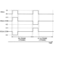
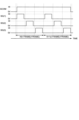
- FIG. 2 is a diagram showing an example of a timing chart for explaining a method of driving the reflector unit cell shown in FIG. 1 .
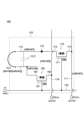
- FIG. 4 is a circuit diagram for explaining a method of driving the reflector unit cell shown in FIG. 3 .
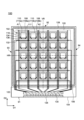
- 1 is a plan view showing an example of a layout of a radio wave reflecting device according to a first embodiment of the present invention.
- FIG. 5 is a plan view showing an example of a layout of the reflector unit cell shown in FIG. 4 .
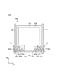
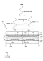
- FIG. 2 is a cross-sectional view showing a cut surface along the A1-A2 line shown in FIG. 1, and is a diagram showing diagrammatically how the propagation direction of a reflected wave is changed by the radio wave reflection device according to the first embodiment of the present invention.
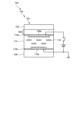
- FIG. FIG. 2 is a diagram illustrating a state of a reflector unit cell according to the first embodiment of the present invention.
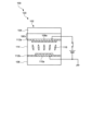
- FIG. 2 is a diagram illustrating a state of a reflector unit cell according to the first embodiment of the present invention.
- FIG. 2 is a diagram illustrating a state of a reflector unit cell according to the first embodiment of the present invention.
- 3 is a circuit diagram for explaining a method of driving the radio wave reflecting device according to the first embodiment of the present invention.
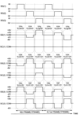
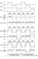
- FIG. 4 is a diagram showing an example of a timing chart for explaining a method of driving the radio wave reflecting device according to the first embodiment of the present invention.
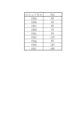
- 4 is a diagram showing the potential difference between the bias electrodes and the common electrodes of a plurality of reflector unit cells of the radio wave reflecting device according to the first embodiment of the present invention.
- FIG. FIG. 5 is a circuit diagram showing a configuration of a radio wave reflecting device according to a second embodiment of the present invention.
- FIG. 11 is a diagram showing an example of a timing chart for explaining a method of driving a radio wave reflecting device according to a second embodiment of the present invention.
- FIG. 11 is a diagram showing an example of a timing chart for explaining a method of driving a radio wave reflecting device according to a second embodiment of the present invention.
- FIG. 11 is a diagram showing an example of a timing chart for explaining a method of driving a radio wave reflecting device according to a second embodiment of the present invention.
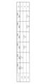
- FIG. 11 is a diagram showing the potential difference between the bias electrodes and the common electrodes of a plurality of reflector unit cells of the radio wave reflecting device according to the second embodiment of the present invention.
- FIG. 11 is a diagram showing the potential difference between the bias electrodes and the common electrodes of a plurality of reflector unit cells of the radio wave reflecting device according to the second embodiment of the present invention.
- FIG. 11 is a diagram showing the potential difference between the bias electrodes and the common electrodes of a plurality of reflector unit cells of the radio wave reflecting device according to the second embodiment of the present invention.
- FIG. 11 is a circuit diagram showing a configuration of a radio wave reflecting device according to a third embodiment of the present invention.
- FIG. 11 is a diagram showing an example of a timing chart for explaining a method of driving a radio wave reflecting device according to a third embodiment of the present invention.
- FIG. 11 is a circuit diagram showing a configuration of a radio wave reflecting device according to a fourth embodiment of the present invention.
- FIG. 13 is a diagram showing an example of a timing chart for explaining a method of driving a radio wave reflecting device according to a fourth embodiment of the present invention.
- the first direction D1 intersects with the second direction D2, and the third direction D3 intersects with the first direction D1 and the second direction D2 (D1D2 plane).
- the first direction D1, the second direction D2, and the third direction D3 correspond to the X direction (x direction), the Y direction (y direction), and the Z direction (z direction).
- Fig. 1 is a functional block diagram showing the configuration of the radio wave reflecting device 100.
- the radio wave reflecting device 100 is a device capable of controlling the traveling direction of a reflected radio wave by using a metasurface (reflector 120) that utilizes a change in dielectric constant due to the orientation state of liquid crystal.
- the radio wave reflecting device 100 includes an IC chip 130 and a reflector 120, and has a configuration capable of biaxial reflection control.
- the reflector 120 includes a plurality of reflector unit cells 102 arranged in a matrix in a first direction D1 and a second direction D2.
- the plurality of reflector unit cells 102 extending in the first direction D1 are arranged in the row direction
- the plurality of reflector unit cells 102 extending in the second direction D2 are arranged in the column direction.
- the plurality of reflector unit cells 102 are arranged in m rows and n columns (the numbers m and n are integers of 2 or more), and the reflector unit cell in the second row and third column may be called the reflector unit cell in the second row and third column.
- the plurality of reflector unit cells 102 includes at least reflector unit cells 102a to 102i. Although details will be described later, each of the plurality of reflector unit cells 102 includes a circuit 103 for driving the reflector unit cell 102, a bias electrode 108 (see FIG. 2), a common electrode 110 (see FIG. 2) that faces the bias electrode 108 and is spaced apart from the bias electrode 108, and a liquid crystal layer 114 (see FIG. 7) that is provided between the bias electrode 108 and the common electrode 110.
- the circuit 103 may include the bias electrode 108 and the common electrode 110.
- each of the multiple reflector unit cells 102 (circuit 103) is electrically connected to a corresponding output signal line 118, a corresponding scanning line 132, and a corresponding common wiring 111.
- the bias electrode 108 of each of the multiple reflector unit cells 102 is electrically connected to a corresponding output signal line 118, and the common electrode 110 of each of the multiple reflector unit cells 102 is electrically connected to a corresponding common wiring 111.
- the IC chip 130 is connected to a plurality of output signal lines 118, a plurality of scanning lines 132, and a plurality of common wirings 111.
- the plurality of output signal lines 118 include output signal lines 118a-118d
- the plurality of scanning lines 132 include scanning lines 132a-132d
- the plurality of common wirings 111 include common wirings 111a-111d.
- the output signal line 118 is supplied with an output signal SS
- the scanning line 132 is supplied with a scanning signal SG
- the common wiring 111 is supplied with a common signal SC.
- the plurality of output signals SS include output signals SS(1)-SS(m)
- the plurality of scanning signals SG include scanning signals SG(1)-SG(n)
- the plurality of common signals SC include common signals SC(1)-SC(m).
- the IC chip 130 can supply signals for driving the reflector unit cells 102 (circuits 103) to each of the reflector unit cells 102 (circuits 103) and control the reflector 120 including the reflector unit cells 102.
- the signals for driving the reflector unit cells 102 (circuits 103) are a scanning signal SG, an output signal SS, a common signal SC, etc.
- the bias electrode 108 and the common electrode 110 of the radio wave reflecting device 100 may be called a first electrode and a second electrode. Also, the IC chip 130 of the radio wave reflecting device 100 may be called a control circuit.
- the multiple reflector unit cells when the multiple radio wave reflecting unit cells are to be distinguished from one another, the multiple reflector unit cells are referred to as multiple reflector unit cells 102a to 102i, and when it is not necessary to distinguish between the multiple radio wave reflecting unit cells, the multiple reflector unit cells are referred to as multiple reflector unit cells 102.
- the multiple output signal lines, multiple output signals, multiple scanning lines, multiple scanning signals, bias electrode 108, common electrode 110, and the like may be called differently depending on whether they are to be distinguished from one another or not.
- the multiple output signal lines may be called the first output signal line 118a to the mth output signal line 118d
- the multiple output signals may be called the first output signal SS(1) to the mth output signal SS(m)
- the multiple scanning lines may be called the scanning lines 132a to 132d
- the multiple scanning signals may be called the first scanning signal SG(1) to the nth scanning signal SG(n).
- FIG. 2 is a schematic circuit diagram showing the configuration of the circuit 103 of the reflector unit cell 102 of the radio wave reflecting device 100. Configurations that are the same as or similar to those in Fig. 1 will be described as necessary.
- the circuit 103 includes, for example, a transistor 160, a transistor 170, a connection portion 115, and a liquid crystal element LCL.
- the transistor 160 includes a gate electrode 161, a source electrode 163, and a drain electrode 164.
- the gate electrode 161 is connected to the scanning line 132.
- the source electrode 163 is connected to the output signal line 118.
- the drain electrode 164 is connected to the first electrode of the liquid crystal element LCL.
- the transistor 170 includes a gate electrode 171, a source electrode 173, and a drain electrode 174.
- the gate electrode 171 is connected to the gate electrode 161 and the scanning line 132.
- the source electrode 173 is connected to the common wiring 111.
- the drain electrode 174 is connected to the second electrode of the liquid crystal element LCL via the connection portion 115.
- the first electrode of the liquid crystal element LCL is electrically connected to the bias electrode 108, and the second electrode of the liquid crystal element LCL is electrically connected to the common electrode 110.
- the first electrode and the second electrode of the liquid crystal element LCL are interchangeable.
- the source electrodes 163 and 173 of the radio wave reflecting device 100 are called source electrodes
- the drain electrodes 164 and 174 are called drain electrodes, but depending on the voltage supplied (applied) to the source and drain electrodes of the transistors 160 and 170, the function of each electrode as a source and the function as a drain may be interchanged.
- the transistor 160 may be called a first switching element
- the transistor 170 may be called a second switching element.
- the driving method of the radio wave reflecting device 100 includes a K+1th radio wave reflection period (K+1stFRAME) after the KthFRAME.
- K+1stFRAME the K+1stFRAME
- the output signal SS(m) and common signal SC(m) are inverted compared to the KthFRAME. That is, in the K+1stFRAME, the output signal SS(m) including -V2 is supplied to the output signal line 118 and the source electrode 163 of the transistor 160, and the common signal SC(m) including +V1 is supplied to the common wiring 111 and the source electrode 173 of the transistor 170. All other points are the same as in the KthFRAME.
- Fig. 5 is a plan view showing an example of the layout of the radio wave reflecting device 100.
- the area of the dielectric substrate 104 other than where the dielectric substrate 104 and the opposing substrate 106 overlap is called the peripheral area 122.
- the peripheral area 122 includes an IC chip 130 and a terminal portion 126 arranged on the dielectric substrate 104.
- the terminal portion 126 is an area that forms a connection with an external circuit.
- a flexible printed circuit (not shown) is connected to the terminal portion 126.
- a signal that controls the IC chip 130 is input from the flexible printed circuit to the terminal portion 126.
- the IC chip 130 shown in FIG. 5 is disposed on the dielectric substrate 104 (array layer 180 (see FIG. 7)) using the COG (chip on glass) method.
- the configuration of the IC chip 130 is not limited to the above, and for example, the IC chip 130 may be disposed on an FPC (flexible printed circuits) connected to the terminal portion 126, or may be configured to be mounted using the COF (chip on film, chip on flexible, etc.) method.
- the multiple bias electrodes 108 are arranged on the dielectric substrate 104 in a matrix in the first direction D1 and the second direction D2.
- the multiple output signal lines 118 arranged on the dielectric substrate 104 extend in the second direction D2 and into the peripheral region 122, and are connected to the IC chip 130.
- the multiple output signal lines 118 are supplied with an output signal SS corresponding to each of the multiple output signal lines 118 from the IC chip 130.
- the multiple scanning lines 132 arranged on the dielectric substrate 104 extend, for example, in the first direction D1 and are connected to the IC chip 130.
- the multiple scanning lines 132 are supplied with a scanning signal SG corresponding to each of the multiple scanning lines 132 from the IC chip 130.
- the multiple common wirings 111 arranged on the dielectric substrate 104 extend, for example, in the second direction D2 and are connected to the IC chip 130.
- the multiple common wirings 111 are supplied with a common signal SC corresponding to each of the multiple common wirings 111 from the IC chip 130.
- the switching element 134 is a transistor 160 (see FIG. 2) including a semiconductor layer 142a, a gate electrode 161, a source electrode 163, and a drain electrode 164.
- the switching element 134 is connected to the output signal line 118 via a contact hole 163a, and is connected to the bias electrode 108 via a contact hole 164a. That is, the switching element 134 connects the output signal line 118 and the bias electrode 108.
- the switching element 136 is a transistor 170 (see FIG. 2) including a semiconductor layer 142b, a gate electrode 171, a source electrode 173, and a drain electrode 174.
- connection portion 115 can be changed as appropriate depending on the application or specifications of the radio wave reflection device 100, the specifications of the power transmitting member, etc.
- the radio wave reflecting device 100 can control the direction of travel of the reflected wave incident on the reflector 120 in the left-right direction of the drawing, with the reflection axis VR parallel to the second direction D2 (Y direction) as the central axis, and can also control the direction of travel of the reflected wave in the up-down direction of the drawing, with the reflection axis HR parallel to the first direction D1 (X direction) as the central axis.
- the radio wave reflecting device 100 includes a reflection axis VR parallel to the second direction D2 (Y direction) and a reflection axis VH parallel to the first direction D1 (X direction), and can control the reflection angle in the direction about the reflection axis VR as the rotation axis and in the direction about the reflection axis HR as the rotation axis.
- the bias electrode 108 has a side length according to the frequency of the radio wave, and the multiple bias electrodes 108 are formed as a collection of rectangles. In other words, the multiple bias electrodes 108 form the radio wave reflection surface of the radio wave reflection device 100.
- the multiple bias electrodes 108 and the multiple common electrodes 110 are formed separately so that the potential can be individually supplied (applied) to the liquid crystal.
- the common electrodes 110 are also arranged so as to overlap with the bias electrodes 108.
- switching elements 134a to 134d When it is necessary to distinguish between the multiple switching elements of the reflector unit cells 102a to 102i, they are called switching elements 134a to 134d or switching elements 136a to 136d, and when it is not necessary to distinguish between the multiple switching elements, they are called multiple switching elements 134 or switching elements 136.
- Fig. 7 is a diagram showing a schematic diagram of the reflection wave changing direction by the reflector 120, and is a diagram showing a schematic cross section along A1-A2 shown in Fig. 1.
- Fig. 8 is a diagram showing a state in which no potential difference occurs between the bias electrode 108 and the common electrode 110 in the reflector unit cell 102.
- Fig. 9 is a diagram showing a state in which a potential difference occurs between the bias electrode 108 and the common electrode 110 in the reflector unit cell 102. Descriptions of configurations that are the same as or similar to those in Figs. 1 to 6 will be omitted here.
- a plurality of common electrodes 110 and a plurality of common wirings 111a to 111d are provided on the first surface 106a of the counter substrate 106.
- An alignment film 112b is provided on the plurality of common electrodes 110 and the plurality of common wirings 111a to 111d.
- An array layer 180 including switching elements 134 and the like and a bias electrode 108 are provided on the first surface 104a of the dielectric substrate 104.
- the first surface 104a of the dielectric substrate 104 is disposed so as to face the first surface 106a of the counter substrate 106.
- a liquid crystal layer 114 is provided between the alignment films 112a and 112b.
- a spacer may be provided between the dielectric substrate 104 and the counter substrate 106 to maintain a constant distance.
- the layers formed on the dielectric substrate 104 are formed using, for example, the following materials.
- the semiconductor layer 142 is formed of a silicon semiconductor such as amorphous silicon or polycrystalline silicon, or an oxide semiconductor including a metal oxide such as indium oxide, zinc oxide, or gallium oxide.
- the gate electrode 161 may be formed of, for example, molybdenum (Mo), tungsten (W), or an alloy thereof.
- the output signal line 118, the common wiring 111, and the scanning line 132 are formed using a metal material such as titanium (Ti), aluminum (Al), or molybdenum (Mo).
- the bias electrode 108, the common electrode 110, and the common wirings 111a to 111d are formed of a metal film such as aluminum (Al) or copper (Cu), or a transparent conductive film such as indium tin oxide (ITO).
- the phase of the reflected wave R1 reflected by the reflector unit cell 102a is different from the phase of the reflected wave R2 reflected by the reflector unit cell 102b, and the traveling direction of the reflected wave changes obliquely in appearance.
- the phase of the reflected wave R2 leads the phase of the reflected wave R1.
- the orientation state of the liquid crystal molecules 116 in the liquid crystal layer 114 changes in response to the output signal SS supplied to the bias electrode 108 and the common signal SC supplied to the common electrode 110, but does not change much with the frequency of the radio waves incident on the bias electrode 108. Therefore, the reflector unit cell 102 can control the phase of the reflected radio waves without being affected by the incident radio waves.
- FIG. 8 shows a state where no potential difference occurs between the bias electrode 108 and the common electrode 110 (referred to as the "first state").
- FIG. 8 shows a case where the alignment films 112a and 112b are horizontal alignment films. In the first state, the long axes of the liquid crystal molecules 116 are aligned horizontally to the surface of the bias electrode 108 by the alignment films 112a and 112b.
- FIG. 9 shows a state in which an output signal SS is supplied to the bias electrode 108 (referred to as the "second state").
- the liquid crystal molecules 116 are subjected to the action of an electric field so that their long axes are oriented perpendicular to the surface of the bias electrode 108.
- the angle at which the long axes of the liquid crystal molecules 116 are oriented can be changed depending on the potential of the output signal SS supplied to the bias electrode 108 and the potential of the common signal SC supplied to the common electrode 110.
- the long axes of the liquid crystal molecules 116 can be oriented in a direction halfway between the horizontal and vertical directions.
- FIG. 10 is a diagram showing a state in which a voltage is supplied (applied) between the bias electrode 108 and the common electrode 110 in the reflector unit cell 102 used in the radio wave reflecting device 100.
- Fig. 11 is a circuit diagram for explaining an example of a method for driving the radio wave reflecting device 100.
- Fig. 12 is a diagram showing an example of a timing chart for explaining the method for driving the radio wave reflecting device 100.
- Fig. 13 is a diagram showing a potential difference VLC between the bias electrode 108 and the common electrode 110 of a plurality of reflector unit cells 102. Descriptions of configurations that are the same as or similar to those in Figs. 1 to 9 will be omitted here.
- the potential difference VLC between the bias electrode 108 and the common electrode 110 of each of the reflector unit cells 102a to 102i is supplied to have the value shown in Figure 13.
- a blank period may be included between the period in which the on signal of the scanning signal SG(3) in the Kth FRAME is supplied and the period in which the on signal of the scanning signal SG(1) in the K+1st FRAME is supplied. Also, a blank period may be included between the periods in which on signals are supplied to adjacent scanning lines.
- the bias electrode 108a is electrically connected to the output signal line 118a via the switching element 134a.
- the switching element 134a is turned on by receiving the scanning signal SG(1) from the IC chip 130 via the scanning line 132a (see FIG. 11). Therefore, the bias electrode 108a is electrically connected to the output signal line 118a via the switching element 134a, and the output signal SS(1) is supplied from the IC chip 130 via the output signal line 118a.
- the switching element 136a is electrically connected to the scanning signal SG(1) from the IC chip 130 via the scanning line 132a (see FIG. 11), and the switching element 136a is turned on.
- the method of driving the reflector unit cell 102a in the K+1st FRAME includes supplying a signal to the reflector unit cell 102a similar to the method of driving the reflector unit cell 102a in the Kth FRAME, and the potential difference VLCa applied between the bias electrode 108a and the common electrode 110a (potential difference applied to the liquid crystal element CLCa) is 0V.
- the scanning signal SG(1) containing the potential LO is supplied to the scanning line 132a and the transistors 160b and 170b of the reflector unit cell 102b, and the transistors 160b and 170b are in the off state.
- common electrode 110e is connected to common electrode 110b via common electrode connection line 211b, 0V is supplied to common electrode 110b. Therefore, the potential supplied to common electrode 110b is the same as when scanning signal SG(1) containing potential HI is supplied to scanning line 132a.
- the potential difference VLCb applied between bias electrode 108b and common electrode 110b remains at 4V.
- the method of driving the reflector unit cell 102f of the radio wave reflecting device 200 in KthFRAME includes supplying an output signal SS(3) including -4V to the output signal line 118c and the transistor 160f, and supplying a common signal SC(3) including +8V to the common wiring 111c and the transistor 170f.
- -4V is supplied to the bias electrode 108f
- +8V is supplied to the common electrode 110f
- the potential difference VLCf applied between the bias electrode 108f and the common electrode 110f is
- the scanning signal SG(1) including the potential LO is supplied to the scanning line 132a and the transistors 160c and 170c of the reflector unit cell 102c, and the transistors 160c and 170c are in the off state.
- the common electrode 110c holds 0V when the scanning signal SG(1) including the potential HI is supplied to the scanning line 132a, and the bias electrode 108c holds +8V when the scanning signal SG(1) including the potential HI is supplied to the scanning line 132a.
- the common electrode 110f is connected to the common electrode 110c via the common electrode connection line 211c, +8V is supplied to the common electrode 110c.
- the potential supplied to the common electrode 110c varies from 0V to +8V, and due to coupling between the common electrode 110c and the bias electrode 108c, the potential supplied to the bias electrode 108c varies from +8V to +16V (see Figures 16 and 18).
- the potential difference VLCc applied between the bias electrode 108c and the common electrode 110c can be maintained at 8V.
- the method of driving the reflector unit cell 102h of the radio wave reflecting device 200 in KthFRAME includes supplying an output signal SS(2) including -8V to the output signal line 118b and the transistor 160h, and supplying a common signal SC(2) including +4V to the common wiring 111b and the transistor 170h.
- -8V is supplied to the bias electrode 108h
- +4V is supplied to the common electrode 110h
- the potential difference VLCh applied between the bias electrode 108h and the common electrode 110h (the potential difference applied to the liquid crystal element CLCh) is
- the scanning signal SG(1) including the potential LO is supplied to the scanning line 132a and the transistors 160b and 170b of the reflector unit cell 102b, and the transistors 160b and 170b are in the OFF state.
- the common electrode 110b holds 0V when the scanning signal SG(1) including the potential HI is supplied to the scanning line 132a
- the bias electrode 108b holds -4V when the scanning signal SG(1) including the potential HI is supplied to the scanning line 132a.
- the scanning signal SG(2) including the potential LO is supplied to the scanning line 132b and the transistors 160e and 170e of the reflector unit cell 102e, and the transistors 160e and 170e are in the OFF state.
- the common electrode 110e holds 0V when the scanning signal SG(2) including the potential HI is supplied to the scanning line 132b, and the bias electrode 108e holds +8 when the scanning signal SG(1) including the potential HI is supplied to the scanning line 132a.
- the common electrodes 110b and 110e are connected to the common electrode 110h via the common electrode connection line 211b, +4V is supplied to the common electrodes 110b and 110e. Therefore, the potential supplied to the common electrode 110b changes from 0V to +4V, and the potential supplied to the bias electrode 108b changes from -4V to 0V due to the coupling between the common electrode 110b and the bias electrode 108b (see Figures 15 and 19).
- the potential difference VLCb given between the bias electrode 108b and the common electrode 110b can be maintained at 4V.
- the potential supplied to the common electrode 110e varies from 0V to +4V, and due to coupling between the common electrode 110e and the bias electrode 108e, the potential supplied to the bias electrode 108e varies from +8V to +12V (see Figures 15 and 19).
- the potential difference VLCe applied between the bias electrode 108b and the common electrode 110b can be maintained at 8V.
- the method of driving the reflector unit cell 102i of the radio wave reflecting device 200 in KthFRAME includes supplying an output signal SS(3) including +8V to the output signal line 118c and the transistor 160i, and supplying a common signal SC(3) including -8V to the common wiring 111c and the transistor 170i.
- +8V is supplied to the bias electrode 108i
- -8V is supplied to the common electrode 110i
- the potential difference VLCi potential difference applied to the liquid crystal element CLCi
- the scanning signal SG(1) including the potential LO is supplied to the scanning line 132a and the transistors 160c and 170c of the reflector unit cell 102c, and the transistors 160c and 170c are in the off state.
- the common electrode 110c holds +16V that fluctuated due to coupling when the scanning signal SG(2) including the potential HI is supplied to the scanning line 132b
- the bias electrode 108c holds +8V that fluctuated due to coupling when the scanning signal SG(2) including the potential HI is supplied to the scanning line 132b.
- the scanning signal SG(2) including the potential LO is supplied to the scanning line 132b and the transistors 160f and 170f of the reflector unit cell 102f, and the transistors 160f and 170f are in the off state.
- the common electrode 110f holds +8V when the scanning signal SG(2) including the potential HI is supplied to the scanning line 132b, and the bias electrode 108f holds -4V when the scanning signal SG(2) including the potential HI is supplied to the scanning line 132b.
- the common electrode 110i is connected to the common electrode 110c and the common electrode 110f via the common electrode connection line 211c, -8V is supplied to the common electrode 110c and the common electrode 110f.
- the potential supplied to the common electrode 110c changes from +8V to 0V
- the potential supplied to the bias electrode 108c changes from +16V to +8V due to the coupling between the common electrode 110c and the bias electrode 108c (see Figures 16 and 19).
- the potential difference VLCc given to the bias electrode 108c and the common electrode 110c can be maintained at 8V.
- the potential supplied to the common electrode 110f varies from +8V to 0V, and due to coupling between the common electrode 110f and the bias electrode 108f, the potential supplied to the bias electrode 108f varies from -4V to -12V (see Figures 15 and 19).
- the potential difference VLCe applied between the bias electrode 108b and the common electrode 110b can be maintained at 12V.
- the common electrodes of adjacent reflector unit cells are electrically connected along the direction in which the common wiring extends to form a common electrode group.
- the driving method of the radio wave reflecting device 200 like the driving method of the radio wave reflecting device 100, includes supplying output signals of mutually inverted polarity to output signal lines connected to adjacent reflector unit cells, and supplying common signals of mutually inverted polarity to common wirings connected to adjacent reflector unit cells.
- the radio wave reflecting device 200 can supply signals (electric potentials) of mutually inverted polarity to the bias electrode 108 or the common electrode 110, and can maintain the electric potential difference between the common electrode and the bias electrode by coupling the common electrode and the bias electrode.
- the radio wave reflecting device 200 can increase the electric potential difference between the bias electrode 108 and the common electrode 110 by coupling the bias electrode 108 and the common electrode 110, and can increase the number of such electric potential differences, compared to when signals (electric potentials) of mutually inverted polarity are not supplied to the bias electrode 108 and the common electrode 110. Therefore, the radio wave reflecting device 100 can reflect radio waves in directions according to many phases.
- a radio wave reflecting device 300 according to a third embodiment will be described with reference to FIGS.
- FIG. 20 is a circuit diagram showing the configuration of the radio wave reflecting device 300.
- FIG. 21 is a diagram showing an example of a timing chart for explaining a method for driving the radio wave reflecting device 300. Explanations of configurations that are the same as or similar to those in FIGS. 1 to 19 will be omitted here.
- the configuration of the reflector unit cell 302 of the radio wave reflecting device 300 is different from the configurations of the reflector unit cell 102 of the radio wave reflecting device 100 (reflector 120) and the reflector unit cell 102 of the radio wave reflecting device 200 (reflector 220). More specifically, the configuration related to the transistor 370 of the reflector unit cell 302 is different from the configuration related to the transistor 170 included in the reflector unit cell 102 of the radio wave reflecting device 200 (reflector 220).
- the transistor 170 included in the reflector unit cell 102 of the radio wave reflecting device 200 (reflector 220) is provided for each reflector unit cell 102, and the common electrodes 110 of three adjacent reflector unit cells are electrically connected along the direction in which the common wiring 111 extends to form one common electrode group 210.
- the transistor 370 corresponds to the transistor 170 included in the reflector unit cell 102 of the radio wave reflecting device 200 (reflector 220).
- One transistor 370 is provided in each of three reflector unit cells 302 adjacent to each other along the direction in which the common wiring 111 extends.
- the common electrodes 110 of the three reflector unit cells 302 adjacent to each other along the direction in which the common wiring 111 extends are electrically connected to form one common electrode group 310.
- the common electrodes of the three reflector unit cells are electrically connected to form one common electrode group 310, but the number of common electrodes that form the common electrode group 210 can be appropriately selected depending on the application and specifications of the radio wave reflecting device 300.
- one transistor 370a is provided for each of three reflector unit cells 302a, 302d, and 302g that are adjacent along the direction in which the common wiring 111a extends. That is, the transistor 370a is provided in common to the three reflector unit cells 302a, 302d, and 302g.
- the common electrodes 110a, 110d, and 110g of the three reflector unit cells 302a, 302d, and 302g that are adjacent along the direction in which the common wiring 111a extends are electrically connected to form one common electrode group 310a.
- the transistor 370a includes a gate electrode 371a, a source electrode 373a, and a drain electrode 374a.
- the gate electrode 371a is connected to a common control line 332.
- the common control line 332 is supplied with a common control signal GCOM.
- the source electrode 373a is connected to a common wiring 111a.
- the drain electrode 374a is electrically connected to the common electrode group 310a (common electrodes 110a, 110d, and 110g) via a connection portion 315a.
- the connection portion 315a can be configured in the same manner as the connection portion 115a.
- Transistors 370b and 370c have the same configuration as transistor 370a, and will be described as necessary. Note that transistors 370b and 370c are connected to the common control line 332, just like transistor 370a.
- transistors 370a to 370c are switching elements similar to transistor 170, and switching (on and off) is controlled by a common control signal GCOM supplied to common control line 332.
- a common control signal GCOM including a potential HI is supplied to common control line 332 and transistors 370a to 370c, transistors 370a to 370c are turned on at the same timing, and the source electrodes and drain electrodes of transistors 370a to 370c become conductive.
- common signals SC(1) to SC(3) supplied to the corresponding common wirings 111a to 111c are supplied to each drain electrode 374, i.e., each common electrode group 310.
- the scanning signals SG(1) to SG(3) supplied corresponding to the scanning lines 132a to 132c, the output signals SS(1) to SS(3) supplied corresponding to the output signal lines 118a to 118c, and the common signals SC(1) to SS(3) supplied corresponding to the common wirings 111a to 111c are the same as those in the first or second embodiment.
- the driving method of each reflector unit cell in the third embodiment may be the same as those in the first and second embodiments, and the driving methods of the first and second embodiments can be changed as appropriate according to the third embodiment.
- a radio wave reflecting device 400 according to a fourth embodiment will be described with reference to FIGS.
- the common electrodes of the three reflector unit cells are electrically connected to form one common electrode group 410, and the common electrodes of the three reflector unit cells are electrically connected to one of the transistors 170 included in the three reflector unit cells.
- the number of common electrodes constituting the common electrode group 410 and any one of the transistors 170 to which each common electrode is connected can be selected appropriately depending on the application, specifications, etc. of the radio wave reflecting device 400.
- the common electrodes 110a to 110c included in three reflector unit cells 402a to 402c adjacent to each other in the direction in which the scanning line 132a extends are electrically connected to each other using a common electrode connection line 411a to form one common electrode group 410a.
- the common electrodes 110d to 110f included in three reflector unit cells 402d to 402f adjacent to each other in the direction in which the scanning line 132b extends are electrically connected to each other using a common electrode connection line 411a to form one common electrode group 410a. That is, the common electrodes 110a to 110f included in the three reflector unit cells 402a to 402f are electrically connected to each other using a common electrode connection line 411a to form one common electrode group 410a.
- the common electrodes 110a to 110c included in the three reflector unit cells 402a to 402c adjacent to each other in the direction in which the scanning line 132a extends are electrically connected to one of the transistors 170a to 170c included in the reflector unit cells 402a to 402c via the connection portion 415c.
- the transistor 170a is electrically connected to the common wiring 111a but is not connected to any of the common electrodes 110
- the transistor 170b is electrically connected to the common wiring 111b but is not connected to any of the common electrodes 110. Therefore, the common electrodes 110a to 110c are controlled by the scanning signal GS(1) supplied to the scanning line 132a and the common signal SC(3) supplied to the common wiring 111c.
- the common electrodes 110d-110f included in the three reflector unit cells 402d-402f adjacent to each other in the direction in which the scanning line 132b extends are electrically connected to one transistor 170f among the transistors 170d-170f included in the reflector unit cells 402d-402f via the connection portion 415f.
- the transistor 170d is electrically connected to the common wiring 111a but is not connected to any of the common electrodes 110
- the transistor 170e is electrically connected to the common wiring 111b but is not connected to any of the common electrodes 110. Therefore, the common electrodes 110d-110f are controlled using the transistor 170f. More specifically, the common electrodes 110d-110f are controlled by the scanning signal GS(2) supplied to the scanning line 132b and the common signal SC(3) supplied to the common wiring 111c.
- the common electrodes 110g-110i included in three reflector unit cells 402g-402i adjacent to each other in the direction in which the scanning line 132c extends are electrically connected to each other using the common electrode connection line 411b to form one common electrode group 410b. Furthermore, the common electrodes 110g-110i included in three reflector unit cells 402g-402i adjacent to each other in the direction in which the scanning line 132c extends are electrically connected to one transistor 170h among the transistors 170g-170i included in the reflector unit cells 402g-402i via the connection portion 415h.
- the transistor 170g is electrically connected to the common wiring 111a but is not connected to any of the common electrodes 110
- the transistor 170i is electrically connected to the common wiring 111c but is not connected to any of the common electrodes 110. Therefore, the common electrodes 110g to 110i are controlled using the transistor 170f. More specifically, the common electrodes 110g to 110i are controlled by a scanning signal GS(3) supplied to the scanning line 132c and a common signal SC(2) supplied to the common wiring 111b.
- the scanning signals SG(1) to SG(3) supplied corresponding to the scanning lines 132a to 132c, the output signal SS(1) supplied corresponding to the output signal line 118a, and the common signal SC(1) supplied corresponding to the common wiring 111a are the same as the signals shown in FIG. 12. Also, as an example, the potential difference VLC between the bias electrode 108 and the common electrode 110 of each of the reflector unit cells 102a to 102i is supplied to have the value shown in FIG. 13, as in the first embodiment.
- the driving method of the radio wave reflection device 400 in KthFRAME includes supplying a scanning signal SG(1) including a potential HI to the scanning line 132a.
- a scanning signal SG(1) including a potential HI is supplied to the scanning line 132a
- the transistors 160 of the reflector unit cells 102a to 102c are turned on, and an output signal SS(1) including a COM potential (0V) is supplied to the bias electrode 108a, an output signal SS(2) including a potential HI is supplied to the bias electrode 108b, and an output signal SS(3) including a potential HI is supplied to the bias electrode 108c.
- the output signal lines and bias electrodes connected to adjacent reflector unit cells are supplied with potentials of the same polarity.
- the transistor 170c is turned on, and a common signal SC(3) including the COM potential (0V) is supplied to the common electrodes 110a to 110c.
- the potential difference VLCa becomes 0V
- VLCb becomes 4V
- VLCc becomes 8V.
- the driving method of the radio wave reflecting device 400 in KthFRAME includes supplying a scanning signal SG(2) including a potential HI to the scanning line 132a, and supplying a scanning signal SG(1) including a potential LO to the scanning line 132a. Based on the scanning signal SG(1) including potential LO being supplied to the scanning line 132a, the transistors 160 of the reflector unit cells 102a to 102c are turned off, the potential difference VLCa is maintained at 0V, VLCb is maintained at 4V, and VLCc is maintained at 8V.
- the transistor 160 of the reflector unit cells 102d to 102f is turned on, the output signal SS(1) including the COM potential (0V) is supplied to the bias electrode 108d, the output signal SS(2) including -4V is supplied to the bias electrode 108e, and the output signal SS(3) including -8V is supplied to the bias electrode 108f. That is, the output signal lines and bias electrodes connected to the adjacent reflector unit cells are supplied with potentials of the same polarity. Also, the transistor 170f is turned on, and the common signal SC(3) including +4V is supplied to the common electrodes 110d to 110f. As a result, the potential difference VLCd becomes 4V (
- the driving method of the radio wave reflecting device 400 in KthFRAME includes supplying a scanning signal SG(3) including a potential HI to the scanning line 132a, supplying a scanning signal SG(1) including a potential LO to the scanning line 132a, and supplying a scanning signal SG(2) including a potential LO to the scanning line 132b.
- the transistors 160 of the reflector unit cells 102a to 102c are turned off, the potential difference VLCa is maintained at 0V, VLCb is maintained at 4V, and VLCc is maintained at 8V.
- the transistors 160 of the reflector unit cells 102d to 102f are turned off, the potential difference VLCd is maintained at 4 V, VLCe is maintained at 8 V, and VLCc is maintained at 12 V.
- the transistors 160 of the reflector unit cells 102g to 102i are turned on, the output signal SS(1) including the COM potential (0 V) is supplied to the bias electrode 108g, the output signal SS(2) including +4 V is supplied to the bias electrode 108h, and the output signal SS(3) including +8 V is supplied to the bias electrode 108i. That is, the output signal lines and bias electrodes connected to the adjacent reflector unit cells are supplied with potentials of the same polarity. Furthermore, transistor 170h is turned on, and a common signal SC(2) containing -8V is supplied to common electrodes 110g to 110i. As a result, the potential difference VLCg becomes 8V (
- the driving method of the radio wave reflecting device 400 in the K+1st FRAME refers to the driving method described in the driving method of the radio wave reflecting device 400 in the Kth FRAME, and includes the driving methods shown in Figures 13 and 23.
- the common electrodes 110 included in the plurality of reflector unit cells 402 adjacent in the direction in which the scanning line 132 extends are electrically connected to each other to form one common electrode group 410, and are electrically connected to one of the transistors 170 included in the plurality of reflector unit cells 402 adjacent in the direction in which the scanning line 132 extends.
- the signals supplied to the bias electrode and common electrode of one reflector unit cell are signals with mutually inverted polarities, and the potentials supplied to the output signal line and bias electrode connected to adjacent reflector unit cells are potentials of the same polarity.
- the driving method of the radio wave reflecting device 400 includes supplying the output signal supplied to the bias electrode of one reflector unit cell and the common signal supplied to the common electrode of the one reflector unit cell with mutually inverted polarities.
- the radio wave reflecting device 400 can increase the potential difference provided between the bias electrode 108 and the common electrode 110 and can increase the number of potential differences compared to when signals (potentials) with inverted polarities are not supplied to the bias electrode 108 and the common electrode 110. Therefore, the radio wave reflecting device 100 can reflect radio waves in directions corresponding to many phases.
- the various configurations of the radio wave reflecting device exemplified as one embodiment of the present invention and the various configurations of the driving method of the radio wave reflecting device may be appropriately combined as long as they are not mutually contradictory. Furthermore, the various configurations of the radio wave reflecting device exemplified as one embodiment of the present invention and the various configurations of the driving method of the radio wave reflecting device may be appropriately interchanged as long as they are not mutually contradictory. Those in which a person skilled in the art has appropriately added, deleted or modified components, or added, omitted or changed conditions of a process based on the radio wave reflecting device and the driving method of the radio wave reflecting device disclosed in this specification and drawings, are also included in the scope of the present invention as long as they include the gist of the present invention.
Landscapes
- Physics & Mathematics (AREA)
- Nonlinear Science (AREA)
- General Physics & Mathematics (AREA)
- Engineering & Computer Science (AREA)
- Electromagnetism (AREA)
- Mathematical Physics (AREA)
- Chemical & Material Sciences (AREA)
- Crystallography & Structural Chemistry (AREA)
- Optics & Photonics (AREA)
- Computer Hardware Design (AREA)
- Theoretical Computer Science (AREA)
- Aerials With Secondary Devices (AREA)
Abstract
第1の電極と、前記第1の電極に対向し、前記第1の電極と離隔して設けられる第2の電極と、前記第1の電極と前記第2の電極との間に設けられた液晶層と、を有する反射板ユニットセルを含み、反射した電波の進行方向を制御可能に構成された電波反射装置の駆動方法は、第1の電位を前記第1の電極に印加し、前記第1の電位と極性が異なる第2の電位を、前記第2の電極に印加すること、を含む。
Description
本発明の実施形態の一つは、反射した電波の進行方向を制御可能な電波反射装置の駆動方法に関する。
近年、10GHz~100GHzの高周波を利用したデバイスが多く普及している。例えば、高周波を利用したデバイスは、面状に配置された複数のアンテナ素子を含むメタサーフェスを含む。所定の位相に対応した電位を含む信号が複数のアンテナ素子のそれぞれに印加されることによって、メタサーフェスは、複数のアンテナ素子のそれぞれが固定された状態で、アンテナの指向性を制御することができる。その結果、メタサーフェスを含む高周波デバイスは、電波の伝送方向を変えて、障害物を避けて通信エリアを広げることができる。
例えば、特許文献1及び2は、複数のアンテナ素子のそれぞれに印加する信号の振幅及び位相を調整し、液晶の配向状態による誘電率の変化を利用したメタサーフェスを開示している。
例えば、電波反射装置のアンテナ素子に印加される電位は、液晶表示装置の液晶表示素子に印加される電位より高い。よって、メタサーフェスに代表される電波反射装置などの非表示デバイスの駆動は、液晶表示装置のような表示デバイスの駆動より、高い電位を必要とする。
このような問題に鑑み、本発明の一実施形態は、反射した電波の進行方向を制御可能であるとともに、高い電位を印加可能な電波反射装置の駆動方法を提供することを目的の一つとする。
本発明の実施形態の一つは、第1の電極と、前記第1の電極に対向し、前記第1の電極と離隔して設けられる第2の電極と、前記第1の電極と前記第2の電極との間に設けられた液晶層と、を有する反射板ユニットセルを含み、反射した電波の進行方向を制御可能に構成された電波反射装置の駆動方法であって、第1の電位を前記第1の電極に印加し、前記第1の電位と極性が異なる第2の電位を、前記第2の電極に印加すること、を含む。
本発明の実施形態の一つは、m行n列(m及びnは2以上の整数)のマトリクス状に設けられた複数の反射板ユニットセルを含み、前記複数の反射板ユニットセルのそれぞれは、第1の電極と、前記第1の電極に対向し、前記第1の電極と離隔して設けられる第2の電極と、前記第1の電極と前記第2の電極との間に設けられた液晶層と、を含み、反射した電波の進行方向を制御可能に構成された電波反射装置の駆動方法であって、第1の電位をm-1行n-1列目の反射板ユニットセルの第1の電極に印加し、前記第1の電位と極性が異なる第2の電位を、n-1列目の複数の反射板ユニットセルのそれぞれの第2の電極が接続された第1の電極群に印加すること、を含む。
本発明の実施形態の一つは、m行n列(m及びnは2以上の整数)のマトリクス状に設けられた複数の反射板ユニットセルを含み、前記複数の反射板ユニットセルのそれぞれは、第1の電極と、前記第1の電極に対向し、前記第1の電極と離隔して設けられる第2の電極と、前記第1の電極と前記第2の電極との間に設けられた液晶層と、を含み、反射した電波の進行方向を制御可能に構成された電波反射装置の駆動方法であって、第1の電位をm-1行n-1列目の反射板ユニットセルの第1の電極に印加し、前記第1の電位と極性が異なる第2の電位を、m-1行目の複数の反射板ユニットセルのそれぞれの第2の電極が接続された第1の電極群に印加すること、を含む。
以下、本発明の実施の形態を、図面などを参照しながら説明する。但し、本発明は多くの異なる態様で実施することが可能であり、以下に例示する実施の形態の記載内容に限定して解釈されるものではない。図面は説明をより明確にするため、実際の態様に比べ、各部の幅、厚さ、形状などについて模式的に表される場合があるが、あくまで一例であって、本発明の解釈を限定するものではない。また、本明細書と各図において、既出の図に関して前述したものと同様の要素には、同一の符号(又は数字の後にa、bなどを付した符号)を付して、詳細な説明を適宜省略することがある。さらに各要素に対する「第1」、「第2」と付記された文字は、各要素を区別するために用いられる便宜的な標識であり、特段の説明がない限りそれ以上の意味を有しない。
本明細書において、ある部材又は領域が他の部材又は領域の「上に(又は下に)」あるとする場合、特段の限定がない限りこれは他の部材又は領域の直上(又は直下)にある場合のみでなく他の部材又は領域の上方(又は下方)にある場合を含み、すなわち、他の部材又は領域の上方(又は下方)において間に別の構成要素が含まれている場合も含む。
本願の明細書において、第1方向D1は第2方向D2に交差し、第3方向D3は第1方向D1及び第2方向D2(D1D2平面)に交差する。例えば、第1方向D1、第2方向D2、及び第3方向D3は、X方向(x方向)、Y方向(y方向)、及びZ方向(z方向)に対応する。
本願の明細書において、同一、同じ及び一致という表記を用いている場合、同一及び一致には、設計の範囲での誤差が含まれてもよい。
[第1実施形態]
図1~図15を参照し、第1実施形態に係る電波反射装置100を説明する。
図1~図15を参照し、第1実施形態に係る電波反射装置100を説明する。
[1-1.電波反射装置100の概要]
図1を参照し、電波反射装置100の概要を説明する。図1は、電波反射装置100の構成を示す機能ブロック図である。電波反射装置100は、液晶の配向状態による誘電率の変化を利用したメタサーフェス(反射板120)を用いて、反射した電波の進行方向を制御可能な装置である。
図1を参照し、電波反射装置100の概要を説明する。図1は、電波反射装置100の構成を示す機能ブロック図である。電波反射装置100は、液晶の配向状態による誘電率の変化を利用したメタサーフェス(反射板120)を用いて、反射した電波の進行方向を制御可能な装置である。
電波反射装置100は、ICチップ130及び反射板120を含み、二軸反射制御可能な構成を有する。反射板120は第1方向D1及び第2方向D2にマトリクス状に設けられた複数の反射板ユニットセル102を含む。例えば、第1方向D1に延在する複数の反射板ユニットセル102は行方向に設けられることを示し、第2方向D2に延在する複数の反射板ユニットセル102は列方向に設けられることを示す。例えば、複数の反射板ユニットセル102はm行n列(数値m及びnは2以上の整数)設けられ、2行3列目の反射板ユニットセルは2行3列の反射板ユニットセルと呼ばれる場合がある。
複数の反射板ユニットセル102は、少なくとも、反射板ユニットセル102a~102iを含む。詳細は後述されるが、複数の反射板ユニットセル102のそれぞれは、反射板ユニットセル102を駆動するための回路103、バイアス電極108(図2を参照)、バイアス電極108に対向し、バイアス電極108と離隔して設けられるコモン電極110(図2を参照)、バイアス電極108とコモン電極110との間に設けられた液晶層114(図7を参照)を含む。なお、回路103が、バイアス電極108及びコモン電極110を含んでよい。
また、複数の反射板ユニットセル102(回路103)のそれぞれは、対応する出力信号線118、対応する走査線132及び対応するコモン配線111に電気的に接続される。複数の反射板ユニットセル102のそれぞれのバイアス電極108は対応する出力信号線118に電気的に接続され、複数の反射板ユニットセル102のそれぞれのコモン電極110は対応するコモン配線111に電気的に接続される。
ICチップ130は、複数の出力信号線118、複数の走査線132、及び複数のコモン配線111に接続される。複数の出力信号線118は出力信号線118a~118dを含み、複数の走査線132は走査線132a~132dを含み、複数のコモン配線111はコモン配線111a~111dを含む。出力信号線118は出力信号SSが供給され、走査線132は走査信号SGが供給され、コモン配線111はコモン信号SCが供給される。複数の出力信号SSは出力信号SS(1)~SS(m)を含み、複数の走査信号SGは走査信号SG(1)~SG(n)を含み、複数のコモン信号SCはコモン信号SC(1)~SC(m)を含む。
ICチップ130は、複数の反射板ユニットセル102(回路103)を駆動させる信号などを、それぞれの複数の反射板ユニットセル102(回路103)に供給し、複数の反射板ユニットセル102を含む反射板120を制御することができる。例えば、複数の反射板ユニットセル102(回路103)を駆動させる信号が、走査信号SG、出力信号SS、コモン信号SCなどである。
電波反射装置100のバイアス電極108及びコモン電極110は、第1の電極及び第2の電極と呼ばれる場合がある。また、電波反射装置100のICチップ130は制御回路と呼ばれる場合がある。
また、電波反射装置100では、複数の電波反射ユニットセルのそれぞれを区別する場合には、複数の反射板ユニットセルは複数の反射板ユニットセル102a~102iと呼ばれ、複数の電波反射ユニットセルのそれぞれを区別する必要がない場合には、複数の反射板ユニットセルは複数の反射板ユニットセル102と呼ばれる。複数の反射板ユニットセルと同様に、複数の出力信号線、複数の出力信号、複数の走査線、複数の走査信号、バイアス電極108、コモン電極110なども、それぞれを区別する場合と区別しない場合とで呼び方が変わる場合がある。また、複数の出力信号線は第1の出力信号線118a~第mの出力信号線118dと呼ばれる場合があり、複数の出力信号は第1の出力信号SS(1)~第mの出力信号SS(m)と呼ばれる場合があり、複数の走査線は走査線132a~132dと呼ばれる場合があり、複数の走査信号は第1の走査信号SG(1)~第nの走査信号SG(n)と呼ばれる場合がある。
[1-2.反射板ユニットセル102の回路構成]
図2を参照し、反射板ユニットセル102の回路構成を説明する。図2は電波反射装置100の反射板ユニットセル102の回路103の構成を示す模式的な回路図である。図1と同一、又は類似する構成については、必要に応じて説明する。
図2を参照し、反射板ユニットセル102の回路構成を説明する。図2は電波反射装置100の反射板ユニットセル102の回路103の構成を示す模式的な回路図である。図1と同一、又は類似する構成については、必要に応じて説明する。
回路103は、例えば、トランジスタ160、トランジスタ170、接続部115及び液晶素子LCLを含む。トランジスタ160はゲート電極161、ソース電極163、及びドレイン電極164を含む。ゲート電極161は走査線132に接続されている。ソース電極163は出力信号線118に接続されている。ドレイン電極164は液晶素子LCLの第1電極に接続されている。トランジスタ170はゲート電極171、ソース電極173、及びドレイン電極174を含む。ゲート電極171はゲート電極161及び走査線132に接続されている。ソース電極173はコモン配線111に接続されている。ドレイン電極174は接続部115を介して液晶素子LCLの第2電極に接続されている。液晶素子LCLの第1電極はバイアス電極108に電気的に接続され、液晶素子LCLの第2電極はコモン電極110に電気的に接続されている。
液晶素子LCLの第1電極及び第2電極は可換である。説明の便宜上、電波反射装置100のソース電極163及び173をソース電極とよび、ドレイン電極164及び174をドレイン電極とよぶが、トランジスタ160及び170のソース電極及びドレイン電極に供給(印加)される電圧によって、各々の電極のソースとしての機能とドレインとしての機能とが入れ替わる場合がある。トランジスタ160は第1のスイッチング素子と呼ばれる場合があり、トランジスタ170は第2のスイッチング素子と呼ばれる場合がある。また、複数の電波反射ユニットセルと同様に、複数の液晶素子LCLのそれぞれを区別する場合には、複数の液晶素子は複数の液晶素子LCLa~LCLiと呼ばれ、複数の液晶素子のそれぞれを区別する必要がない場合には、複数の液晶素子は複数の液晶素子LCLと呼ばれる。
[1-3.電波反射装置100(反射板ユニットセル102)の駆動方法の概要]
図3及び図4を参照し、電波反射装置100(反射板ユニットセル102)の駆動方法の概要を説明する。図3は図1に示される反射板ユニットセル102の駆動方法を説明するためのタイミングチャートの一例を示す図である。図4は、図3に示される反射板ユニットセル102の駆動方法を説明するための回路図である。図1及び図2と同一、又は類似する構成については、必要に応じて説明する。
図3及び図4を参照し、電波反射装置100(反射板ユニットセル102)の駆動方法の概要を説明する。図3は図1に示される反射板ユニットセル102の駆動方法を説明するためのタイミングチャートの一例を示す図である。図4は、図3に示される反射板ユニットセル102の駆動方法を説明するための回路図である。図1及び図2と同一、又は類似する構成については、必要に応じて説明する。
電波反射装置100の駆動方法は、電波反射期間(一つのフレーム期間(1FRAME)において、それぞれの反射板ユニットセル102の位相に応じた電位をそれぞれの反射板ユニットセル102に供給することを含む。電波反射装置100の駆動方法は、電波反射期間(1FRAME)において、第1方向D1に配列される複数のバイアス電極108を行ごとに選択することを含む。ICチップ130は、複数の反射板ユニットセル102のそれぞれのスイッチング素子134(トランジスタ160)に、走査線132を介して、所定の反射板ユニットセル102を選択するための走査信号SGを供給する。また、ICチップ130は、複数の反射板ユニットセル102のうち、選択されたスイッチング素子134(トランジスタ160)に電気的に接続されたバイアス電極108に、出力信号線118を介して、それぞれの反射板ユニットセル102の位相に応じた電位を含む出力信号SSを供給する。さらに、ICチップ130は、複数の反射板ユニットセル102のうち、選択されたスイッチング素子136(トランジスタ170)に電気的に接続されたコモン電極110に、コモン配線111を介して、それぞれの反射板ユニットセル102の位相に応じた電位を含むコモン信号SCを供給する。ICチップ130がこの操作を行ごとに実行し、電波反射装置100は、それぞれの反射板ユニットセル102の位相に応じた電位に基づき、反射板ユニットセル102内の液晶素子LCLに含まれる液晶分子116の配向状態を変化させることができる。その結果、電波反射装置100は入射した電波を所望の方向に反射することができる。
また、電波反射装置100の駆動方法は、電波反射期間において、バイアス電極108及びコモン電極110に、互いに極性の異なる信号を供給し、互いに極性の異なる電位を供給(印加)することを含む。例えば、ICチップ130は、複数の反射板ユニットセル102のそれぞれのスイッチング素子134(トランジスタ160)に、走査線132を介して、所定の反射板ユニットセル102を選択するための走査信号SGを供給し、選択されたスイッチング素子134(トランジスタ160)に電気的に接続されたバイアス電極108にプラス極性の第1の電位(+V1)を含む出力信号SSを供給し、選択されたスイッチング素子136(トランジスタ170)に電気的に接続されたコモン電極110にマイナス極性の第2の電位(-V2)を含むコモン信号SCを供給する。すなわち、電波反射装置100は、バイアス電極108とコモン電極110とに、互いに極性の異なる(反転した)第1の電位を供給することができる。その結果、電波反射装置100の焼き付きを抑制することができる。また、バイアス電極108とコモン電極110とに極性の異なる同一の電位を供給した場合には、バイアス電極108とコモン電極110とに与えられる電位差(液晶層114に与えられる電位差)は、理想的には、同一の電位の2倍の電位となる。一般的に、コモン電極110は定電位が供給されるため、電波反射装置100は、定電位がコモン電極110に供給される場合と比較して、液晶層114に大きな電位差を与えることができる。その結果、電波反射装置100は、所定の電位を十分に液晶層114に供給すると共に、液晶層114の液晶分子116(図8を参照)の配向状態による誘電率の変化を安定させることができる。よって、電波反射装置100は、電波の伝送方向を安定させて、電波障害を回避させることができる。
例えば、定電位は、コモン電位(電位COM)であってよく、グラウンド電位(GND電位)であってよく、0Vの電位であってよく、電位VSSであってもよい。例えば、定電位は、出力信号SS及びコモン信号SCの基準となる基準電位である。また、例えば、電位COMは、極性反転信号の中間レベルの電位である。
電波反射装置100では、オン信号が電位ハイ(High、HI)であり、オフ信号が電位ロー(Low、LO)であってよい。また、電波反射装置100では、オン信号が電位LOであり、オフ信号が電位HIであってもよい。電位HIは、電位LOより大きい(高い)。また、電位HIは出力信号SS及びコモン信号SCの最大電位以上であり、電位LOは出力信号SS及びコモン信号SCの最小電位以下である。
また、電波反射装置100では、出力信号SSに供給される電位の極性はコモン信号SC電位に供給される電位の極性と異なり、出力信号SSに供給される電位の極性はコモン信号SCに供給される電位の極性と反転している。すなわち、出力信号SSはコモン信号SCの極性が反転された極性反転信号である。
また、出力信号SSに供給される電位及びコモン信号SC電位に供給される電位は-V2以上+V1以下である。すなわち、出力信号SSに供給される電位及びコモン信号SC電位に供給される最大電位は+V1であり、出力信号SSに供給される電位及びコモン信号SC電位に供給される最小電位は-V2である。なお、出力信号SS及びコモン信号SCに供給される電位がCOM電位の場合には、出力信号SS及びコモン信号SCに供給される電位は同一であり、出力信号SS及びコモン信号SCに供給される電位の極性は反転しない。
例えば、電位COMを中間電位COM電位として、+V1は電位COM及び-V2より高く(大きく)、-V2は電位COM及び+V1より低い(小さい)。例えば、電位COMは0Vであり、-V2は-8Vであり、+V1は+8Vである。
図3及び図4を用いて、電波反射装置100の駆動方法の一例を説明する。例えば、スイッチング素子134及びスイッチング素子136のスイッチング(オン及びオフ)は走査線132に供給される走査信号SG(n)により制御される。すなわち、スイッチング素子134及びスイッチング素子136は同じタイミングでスイッチング(オン及びオフ)される。走査信号SG(n)に応じて、スイッチング素子134がオンになったバイアス電極108は、出力信号線118と導通し、出力信号SS(m)が供給される。走査信号SG(n)に応じて、スイッチング素子136がオンになったコモン電極110は、コモン配線111と導通し、コモン信号SC(m)が供給される。スイッチング素子134及びスイッチング素子136は、例えば、薄膜トランジスタで形成される。
また、図3及び図4を用いて、電波反射装置100の駆動方法の一例を、より具体的に説明する。電波反射装置100の駆動方法は、第K番目の電波反射期間(KthFRAME)を含む。数値Kは1以上の自然数である。KthFRAMEでは、電位HIを含む走査信号SG(n)が走査線132、トランジスタ160のゲート電極161及びトランジスタ170のゲート電極171に供給され、+V1を含む出力信号SS(m)が出力信号線118及びトランジスタ160のソース電極163に供給され、-V2を含むコモン信号SC(m)がコモン配線111及びトランジスタ170のソース電極173に供給される。
その結果、トランジスタ160はオン状態となり、ソース電極163をドレイン電極164と導通(接続)させ、+V1を含む出力信号SS(m)がドレイン電極164及びバイアス電極108に供給される。また、トランジスタ170はオン状態となり、ソース電極173をドレイン電極174と導通(接続)させ、-V2を含むコモン信号SC(m)がドレイン電極174及びコモン電極110に供給される。よって、バイアス電極108とコモン電極110とに与えられる電位差(液晶素子CLCに与えられる電位差)は、+V1-(-V2)=V1+V2となる。+V1=|-V2|の場合には、当該電位差は2×V1(2×|-V2|)となる。
また、電波反射装置100の駆動方法は、KthFRAMEの後に、第K+1番目の電波反射期間(K+1stFRAME)を含む。K+1stFRAMEは、KthFRAMEと比較して、出力信号SS(m)及びコモン信号SC(m)が反転している。すなわち、K+1stFRAMEでは、-V2を含む出力信号SS(m)が出力信号線118及びトランジスタ160のソース電極163に供給され、+V1を含むコモン信号SC(m)がコモン配線111及びトランジスタ170のソース電極173に供給される。それ以外の点は、KthFRAMEと同様である。K+1stFRAMEでバイアス電極108とコモン電極110とに与えられる電位差(液晶素子CLCに与えられる電位差)は、|-V2-(+V1)|=V2+V1となる。+V1=|-V2|の場合には、当該電位差は2×V1(2×|-V2|)となる。
電波反射装置100は、バイアス電極108及びコモン電極110のそれぞれに-V2以上+V1以下のアナログ電位を供給することができる。また、電波反射装置100は、バイアス電極108の電位とコモン電極110の電位とに与えられる電位差を、-V2以上+V1以下の電位と、-V2以上+V1以下の電位との差の絶対値にすることができる。よって、電波反射装置100は、バイアス電極108又はコモン電極110の一方に定電位が供給されていた場合より、当該電位差を大きくすることができると共に、当該電位差の数を増やすことができる。その結果、電波反射装置100は、出力信号SSの極性がコモン信号SCの極性と反転していない電波反射装置より、多くの位相に応じた方向に、電波を反射することができる。
[1-4.電波反射装置100及び反射板ユニットセル102のレイアウト]
図5及び図6を参照し、電波反射装置100及び反射板ユニットセル102のレイアウトの一例及び断面構造の一例を説明する。図5は、電波反射装置100のレイアウトの一例を示す平面図である。図6は、反射板ユニットセル102を下方(電波が入射する側)から見たときのレイアウトの一例を示す平面図であり、より詳細には、出力信号線118とバイアス電極108との間に設けられたスイッチング素子134、コモン配線111とコモン電極110との間に設けられたスイッチング素子136、バイアス電極108、コモン電極110、出力信号線118、コモン配線111及び走査線132の配置を拡大した図である。図1~図4と同一、又は類似する構成については、ここでの説明を省略する。
図5及び図6を参照し、電波反射装置100及び反射板ユニットセル102のレイアウトの一例及び断面構造の一例を説明する。図5は、電波反射装置100のレイアウトの一例を示す平面図である。図6は、反射板ユニットセル102を下方(電波が入射する側)から見たときのレイアウトの一例を示す平面図であり、より詳細には、出力信号線118とバイアス電極108との間に設けられたスイッチング素子134、コモン配線111とコモン電極110との間に設けられたスイッチング素子136、バイアス電極108、コモン電極110、出力信号線118、コモン配線111及び走査線132の配置を拡大した図である。図1~図4と同一、又は類似する構成については、ここでの説明を省略する。
図5に示されるように、電波反射装置100は、誘電体基板104、対向基板106、及び周辺領域122を含む。電波反射装置100(誘電体基板104)は、第1方向D1に沿った第1の辺91と、第2方向D2に沿って第1の辺91と交差する第3の辺93と、第3の辺93と交差すると共に第1の辺91と平行に対向する第2の辺92と、第1の辺91及び第2の辺92と交差すると共に第3の辺93と平行に対向する第4の辺94を有する。対向基板106は誘電体基板104に重畳し、対向基板106はシール材128を用いて誘電体基板104に貼り合わされている。対向基板106、誘電体基板104及びシール材128で囲まれる領域は、液晶層114(図7を参照)を含む。なお、誘電体基板104は第1の基板と呼ばれ、対向基板106は第2の基板と呼ばれる場合がある。
誘電体基板104と対向基板106とが重畳する以外の誘電体基板104の領域は、周辺領域122と呼ばれる。周辺領域122は、誘電体基板104上に配置されたICチップ130及び端子部126を含む。端子部126は、外部回路との接続を形成する領域である。例えば、端子部126には、フレキシブルプリント回路(図示は省略)が接続される。端子部126には、フレキシブルプリント回路からICチップ130を制御する信号が入力される。
例えば、図5に示されるICチップ130は、COG(Chip on Glass)方式を用いて、誘電体基板104(アレイ層180(図7を参照))の上に配置される。なお、ICチップ130の構成は上記に限定されるものではなく、例えば、ICチップ130が端子部126に接続されるFPC(Flexible printed circuits)上に配置されてよく、COF(Chip on Film、又は、Chip on Flexibleなど)方式を用いて実装される構成であってもよい。
複数のバイアス電極108は、第1方向D1及び第2方向D2にマトリクス状に、誘電体基板104上に配設される。
誘電体基板104に配設された複数の出力信号線118は、第2方向D2に延在すると共に周辺領域122に延在し、ICチップ130に接続される。複数の出力信号線118は、ICチップ130から、複数の出力信号線118のそれぞれに応じた出力信号SSを供給される。
誘電体基板104に配設された複数の走査線132は、例えば、第1方向D1に延在し、ICチップ130に接続される。複数の走査線132は、ICチップ130から、複数の走査線132のそれぞれに応じた走査信号SGを供給される。
誘電体基板104に配設された複数のコモン配線111は、例えば、第2方向D2に延在し、ICチップ130に接続される。複数のコモン配線111は、ICチップ130から、複数のコモン配線111のそれぞれに応じたコモン信号SCを供給される。
複数のコモン電極110は、第1方向D1及び第2方向D2にマトリクス状に、対向基板106上に配置される。
図5及び図6に示されるように、反射板ユニットセル102は、コモン電極110、液晶層114(図7を参照)、及びバイアス電極108が平面視で重畳するように配置される。反射板ユニットセル102はスイッチング素子134及びスイッチング素子136を含む。
例えば、スイッチング素子134は、半導体層142a、ゲート電極161、ソース電極163及びドレイン電極164を含むトランジスタ160(図2を参照)である。スイッチング素子134は、コンタクトホール163aを介して出力信号線118と接続され、コンタクトホール164aを介してバイアス電極108とを接続される。すなわち、スイッチング素子134は、出力信号線118とバイアス電極108とを接続する。例えば、スイッチング素子136は、半導体層142b、ゲート電極171、ソース電極173及びドレイン電極174を含むトランジスタ170(図2を参照)である。スイッチング素子136は、コンタクトホール173aを介してコモン配線111と接続され、接続部115を介してコモン電極110と接続される。すなわち、スイッチング素子136は、コモン配線111とコモン電極110とを接続する。その結果、反射板ユニットセル102(スイッチング素子134及びスイッチング素子136)は走査線132、出力信号線118及びコモン配線111に電気的に接続される。
接続部115は誘電体基板104上のスイッチング素子136と対向基板106上のコモン電極110とを接続するため、接続部115は誘電体基板104側の配向膜112a(図7を参照)及び対向基板106側の配向膜112b(図7を参照)を貫通又は除去し形成される。例えば、接続部115は、フォトスペーサ、導電性ビーズなどの導電性部材を含む。液晶層114が誘電体基板104側の配向膜と対向基板106側の配向膜との間に配設されるため、断面視における接続部115は、周囲を液晶層114(図7を参照)で囲まれる。なお、図6に示される接続部115は、コンタクトホール163a、164a、173aと同様のサイズ(面積)として図示されるが、接続部115のサイズは電波反射装置100の用途又は仕様、送電性部材の仕様などに応じて適宜変更可能である。
電波反射装置100は、反射板120に入射された電波を、第2方向D2(Y方向)に平行な反射軸VRを中心軸として、図面の左右方向に反射波の進行方向を制御することができることに加え、第1方向D1(X方向)に平行な反射軸HRを中心軸として図面の上下方向へも反射波の進行方向を制御することができる。すなわち、電波反射装置100は、第2方向D2(Y方向)に平行な反射軸VR、及び第1方向D1(X方向)に平行な反射軸VHを含み、反射軸VRを回転軸とした方向、及び反射軸HRを回転軸とした方向に反射角を制御することができる。
バイアス電極108が電波の周波数に応じた辺長を有し、複数のバイアス電極108が矩形の集合として形成される。すなわち、複数のバイアス電極108が電波反射装置100の電波の反射面を構成する。また、複数のバイアス電極108及び複数のコモン電極110には、液晶に対する電位が個別に供給(印加)可能されるように、複数のバイアス電極108及び複数のコモン電極110は個別に形成される。また、コモン電極110はバイアス電極108と重畳するように配置される。
なお、反射板ユニットセル102a~102iの複数のスイッチング素子のそれぞれを区別する場合には、スイッチング素子134a~134d、又は、スイッチング素子136a~136dと呼び、複数のスイッチング素子のそれぞれを区別する必要がない場合には、複数のスイッチング素子134又はスイッチング素子136と呼ぶ。
[1-5.反射板120(反射板ユニットセル102)の動作の概要]
図7~図9を参照し、反射板120(反射板ユニットセル102)の動作の概要を説明する。図7は、反射板120によって反射波の進行方向が変化することを模式的に示す図であり、図1に示されA1-A2に沿った断面を模式的に示す図である。図8は、反射板ユニットセル102において、バイアス電極108とコモン電極110との間に電位差が生じない状態を模式的に示す図である。図9は、反射板ユニットセル102において、バイアス電極108とコモン電極110との間に電位差が生じた状態を示す図である。図1~図6と同一、又は類似する構成については、ここでの説明を省略する。
図7~図9を参照し、反射板120(反射板ユニットセル102)の動作の概要を説明する。図7は、反射板120によって反射波の進行方向が変化することを模式的に示す図であり、図1に示されA1-A2に沿った断面を模式的に示す図である。図8は、反射板ユニットセル102において、バイアス電極108とコモン電極110との間に電位差が生じない状態を模式的に示す図である。図9は、反射板ユニットセル102において、バイアス電極108とコモン電極110との間に電位差が生じた状態を示す図である。図1~図6と同一、又は類似する構成については、ここでの説明を省略する。
電波反射装置100は、入射波の進行方法に対して反射波の進行方向に電波を反射する。電波反射装置100(反射板ユニットセル102)が反射可能な電波の周波数に制約はない。例えば、反射板ユニットセル102が反射可能な電波の周波数は、400MHz~300GHzである。典型的には、400MHz~6.0GHz帯の電波、2.5GHz~4.7GHz帯の電波、24GHz~300GHz帯の電波の反射に、電波反射装置100を利用することができる。
例えば、一つの反射板ユニットセル102は、誘電体基板104の一部、アレイ層180の一部、一つのバイアス電極108、配向膜112aの一部、液晶層114の一部、配向膜112bの一部、コモン電極110の一部、及び対向基板106の一部を含む。複数の反射板ユニットセル102は、誘電体基板104を共有する。誘電体基板104は一つの層をなす誘電体層とみなすことができる。誘電体基板104は、誘電体層と呼ばれる場合がある。
対向基板106の第1面106aの上には、複数のコモン電極110及び複数のコモン配線111a~111dが設けられる。複数のコモン電極110及び複数のコモン配線111a~111dの上に配向膜112bが設けられる。誘電体基板104の第1面104aの上には、スイッチング素子134などを含むアレイ層180及びバイアス電極108が設けられる。誘電体基板104の第1面104aは、対向基板106の第1面106aに対向するように配置される。配向膜112aと配向膜112bとの間に液晶層114が設けられる。なお、図示は省略されるが、誘電体基板104と対向基板106との間には、間隔を一定に保つためのスペーサが設けられてもよい。
液晶層114の厚さTは、例えば、20μm以上50μm未満であってよく、典型的には、30μm以上40μm未満であってよい。例えば、電波反射装置100の液晶層114の厚さTは、35μmである。液晶層114の厚さTは、液晶表示装置で用いられる液晶層の厚さ(例えば、2.0μm以上5μm以下)より、十分に厚い。
誘電体基板104に形成される各層は、例えば、以下のような材料を用いて形成される。半導体層142は、アモルファスシリコン、多結晶シリコンのようなシリコン半導体、酸化インジウム、酸化亜鉛、酸化ガリウムなどの金属酸化物を含む酸化物半導体で形成される。ゲート電極161は、例えば、モリブデン(Mo)、タングステン(W)又はこれらの合金で構成されてもよい。出力信号線118、コモン配線111及び走査線132は、チタン(Ti)、アルミニウム(Al)、モリブデン(Mo)などの金属材料を用いて形成される。バイアス電極108、コモン電極110及びコモン配線111a~111dは、アルミニウム(Al)、銅(Cu)などの金属膜、酸化インジウムスズ(ITO)などの透明導電膜で形成される。
図7に示されるように、反射板ユニットセル102aはバイアス電極108aを含み、反射板ユニットセル102bはバイアス電極108bを含む。反射板ユニットセル102a及び反射板ユニットセル102bは、第1方向D1(又は第2方向D2)に隣接している。バイアス電極108aは出力信号線118aに電気的に接続され、バイアス電極108bは出力信号線118bに電気的に接続されている。
例えば、反射板ユニットセル102a及び反射板ユニットセル102bに同じ位相で電波が入射した場合には、反射板ユニットセル102aに電位VP1を含む出力信号SS(1)が供給され、反射板ユニットセル102bに電位VP2を含む出力信号SS(2)が供給される。例えば、電位VP1は電位VP2と異なり、電位VP1は電位VP2より大きい(高い)。反射板ユニットセル102bによる反射波の位相の変化は、反射板ユニットセル102aによる反射波の位相の変化より大きい。反射板ユニットセル102aで反射した反射波R1の位相は、反射板ユニットセル102bで反射した反射波R2の位相と異なり、見かけ上、反射波の進行方向が斜め方向に変化する。例えば、図7に示される例では、反射波R2の位相が反射波R1の位相より進んでいる。
バイアス電極108には、液晶層114の液晶分子116の配向を制御する出力信号SSが供給される。例えば、出力信号SSは、直流電圧の信号、又は正の直流電圧と負の直流電圧とが交互に反転する極性反転信号である。一例として、電波反射装置100は、極性反転信号をバイアス電極108に供給する。一例として、コモン電極110には、液晶層114の液晶分子116の配向を制御するコモン信号SCを供給される。例えば、コモン信号SCは、極性反転信号の中間レベルの電位COMである。バイアス電極108に出力信号SSが供給され、コモン電極110にコモン信号SCが供給されると、液晶層114に含まれる液晶分子116の配向状態が変化する。
反射板ユニットセル102は、液晶分子116の配向状態の変化により、液晶層114の誘電率を変化させることができる。その結果、電波反射装置100(反射板120)が、電波を反射するときに、反射波の位相を遅延させることができる。
液晶層114の液晶分子116の配向状態は、バイアス電極108に供給される出力信号SS及びコモン電極110に供給されるコモン信号SCに応じて変化するが、バイアス電極108に入射される電波の周波数にはほとんど追従しない。したがって、反射板ユニットセル102は、入射される電波の影響を受けずに、反射する電波の位相を制御することができる。
図8は、バイアス電極108とコモン電極110との間に電位差が生じない状態(「第1の状態」とする)を示す。図8は、配向膜112a及び配向膜112bが水平配向膜である場合を示す。第1の状態における液晶分子116の長軸は、配向膜112a及び配向膜112bにより、バイアス電極108の表面に対して水平に配向している。
図9は、バイアス電極108に出力信号SSが供給された状態(「第2の状態」とする)を示す。第2の状態において、例えば、液晶分子116は電界の作用を受けて長軸がバイアス電極108の表面に対し垂直に配向する。液晶分子116の長軸が配向する角度は、バイアス電極108に供給される出力信号SSの電位及びコモン電極110に供給されるコモン信号SCの電位に応じて変更可能である。例えば、液晶分子116の長軸は、水平方向と垂直方向との中間の方向に配向させることもできる。
液晶分子116が正の誘電異方性を有する場合には、第1の状態に対して第2の状態の方が、見かけ上の誘電率が大きくなる。また、液晶分子116が負の誘電異方性を有する場合には、第1の状態に対して第2の状態の方が見かけ上の誘電率が小さくなる。誘電異方性を有する液晶層114は、可変誘電体層とみなすことができる。反射板ユニットセル102は、液晶層114の誘電異方性を利用して、反射波の位相を遅延させる(又は遅延させない)ことができる。
[1-6.電波反射装置100の駆動方法]
図10~図13を参照し、電波反射装置100の駆動方法を説明する。図10は、電波反射装置100に用いられる反射板ユニットセル102において、バイアス電極108とコモン電極110との間に電圧が供給(印加)された状態を示す図である。図11は、電波反射装置100の駆動方法の一例を説明するための回路図である。図12は電波反射装置100の駆動方法を説明するためのタイミングチャートの一例を示す図である。図13は複数の反射板ユニットセル102のバイアス電極108とコモン電極110との間の電位差VLCを示す図である。図1~図9と同一、又は類似する構成については、ここでの説明を省略する。
図10~図13を参照し、電波反射装置100の駆動方法を説明する。図10は、電波反射装置100に用いられる反射板ユニットセル102において、バイアス電極108とコモン電極110との間に電圧が供給(印加)された状態を示す図である。図11は、電波反射装置100の駆動方法の一例を説明するための回路図である。図12は電波反射装置100の駆動方法を説明するためのタイミングチャートの一例を示す図である。図13は複数の反射板ユニットセル102のバイアス電極108とコモン電極110との間の電位差VLCを示す図である。図1~図9と同一、又は類似する構成については、ここでの説明を省略する。
図10~図13を参照した電波反射装置100の駆動方法の説明では、一例として、電波反射装置100の駆動方法はKthFRAME及びK+1stFRAMEを含む。KthFRAMEにおける出力信号SS(1)~SS(3)、コモン信号SC(2)及びSC(3)は-8V以上+8V以下の電位が供給される。K+1stFRAMEにおける出力信号SS(1)~SS(3)、コモン信号SC(2)及びSC(3)は、KthFRAMEにおける各信号の極性反転信号が供給される。KthFRAME及びK+1stFRAMEにおけるコモン信号SC(1)は電位LOを供給される。また、COM電位は0Vである。また、一例として、反射板ユニットセル102a~102iのそれぞれのバイアス電極108とコモン電極110との間の電位差VLCは、図13に示される値となるように供給される。なお、KthFRAMEにおける走査信号SG(3)のオン信号が供給される期間と、K+1stFRAMEにおける走査信号SG(1)のオン信号が供給される期間との間は、ブランク期間を含んでよい。また、互いに隣接する走査線にオン信号が供給される期間の間は、ブランク期間を含んでよい。
図10に示されるように、バイアス電極108aは、スイッチング素子134aを介して、出力信号線118aに電気的に接続される。スイッチング素子134aは、走査線132a(図11を参照)を介して、ICチップ130から走査信号SG(1)が供給され、オンになった状態である。よって、バイアス電極108aは、スイッチング素子134aを介して、出力信号線118aと導通し、出力信号線118aを介して、ICチップ130から出力信号SS(1)が供給される。スイッチング素子136aは、走査線132a(図11を参照)を介して、ICチップ130から走査信号SG(1)が供給され、オンになった状態である。よって、コモン電極110aは、スイッチング素子136aを介して、コモン配線111aと導通し、コモン配線111aを介して、ICチップ130からコモン信号SC(1)が供給される。その結果、バイアス電極108aとコモン電極110aとの間に、出力信号SS(1)とコモン信号SC(1)との電位差を与えて、電波反射装置100は、当該電位差に基づく位相に応じた方向に、電波を反射することができる。
図11に一例として示されるように、電波反射装置100の反射板120は、3行3列(m=n=3)の9つの反射板ユニットセル102a~102iを含む。反射板ユニットセル102a~102cは走査線132aに電気的に接続され、反射板ユニットセル102d~102fは走査線132bに電気的に接続され、反射板ユニットセル102g~102iは走査線132cに電気的に接続される。反射板ユニットセル102a、120d及び102gは出力信号線118a及びコモン配線111aに電気的に接続され、反射板ユニットセル102b、120e及び102hは出力信号線118b及びコモン配線111bに電気的に接続され、反射板ユニットセル102c、120f及び102iは出力信号線118c及びコモン配線111cに電気的に接続される。走査線132a~132cは走査信号SG(1)~SG(3)が供給され、出力信号線118a~118cは出力信号SS(1)~SS(3)が供給され、コモン配線111a~111cは、コモン信号SC(1)~SC(3)が供給される。
図11又は図12に示されるように、例えば、KthFRAMEにおける反射板ユニットセル102aの駆動方法は、電位HIを含む走査信号SG(1)が走査線132a、トランジスタ160a及びトランジスタ170aに供給されること、電位COM(0V)を含む出力信号SS(1)が出力信号線118a及びトランジスタ160aに供給されること、電位COM(0V)を含むコモン信号SC(1)がコモン配線111a及びトランジスタ170aに供給されることを含む。その結果、トランジスタ160a及びトランジスタ170aは同じタイミングでオン状態となり、0Vがバイアス電極108aに供給、0Vがコモン電極110aに供給される。よって、バイアス電極108aとコモン電極110aとに与えられる電位差VLCa(液晶素子CLCaに与えられる電位差)は0Vとなる。
K+1stFRAMEにおける反射板ユニットセル102aの駆動方法は、KthFRAMEにおける反射板ユニットセル102aの駆動方法と同様の信号が反射板ユニットセル102aに供給されることを含み、バイアス電極108aとコモン電極110aとに与えられる電位差VLCa(液晶素子CLCaに与えられる電位差)は0Vとなる。
例えば、KthFRAMEにおける反射板ユニットセル102hの駆動方法は、電位HIを含む走査信号SG(3)が走査線132c、トランジスタ160h及びトランジスタ170hに供給されること、-8Vを含む出力信号SS(2)が出力信号線118b及びトランジスタ160hに供給されること、+4を含むコモン信号SC(2)がコモン配線111b及びトランジスタ170hに供給されることを含む。その結果、トランジスタ160hはオン状態となり、-8Vがバイアス電極108hに供給される。また、トランジスタ170iはオン状態となり、-8Vがコモン電極110hに供給される。よって、バイアス電極108hとコモン電極110hとに与えられる電位差VLCh(液晶素子CLChに与えられる電位差)は12Vとなる。
K+1stFRAMEにおける反射板ユニットセル102hの駆動方法は、KthFRAMEにおける出力信号SS(2)及びコモン信号SC(2)が極性反転された信号が反射板ユニットセル102hに供給されることを含む。すなわち、K+1stFRAMEにおける反射板ユニットセル102hの駆動方法は、+8Vを含む出力信号SS(2)が出力信号線118b及びトランジスタ160hに供給されること、-4Vを含むコモン信号SC(2)がコモン配線111h及びトランジスタ170hに供給されることを含む。その結果、バイアス電極108hとコモン電極110hとに与えられる電位差VLCh(液晶素子CLChに与えられる電位差)は、KthFRAMEにおける電位差VLChと同様に、12Vとなる。
また、例えば、KthFRAMEにおける反射板ユニットセル102iの駆動方法は、電位HIを含む走査信号SG(3)が走査線132c、トランジスタ160i及びトランジスタ170iに供給されること、+8Vを含む出力信号SS(3)が出力信号線118c及びトランジスタ160iに供給されること、-8Vを含むコモン信号SC(3)がコモン配線111c及びトランジスタ170iに供給されることを含む。その結果、トランジスタ160iはオン状態となり、+8Vがバイアス電極108iに供給される。また、トランジスタ170iはオン状態となり、-8Vがコモン電極110aに供給される。よって、バイアス電極108iとコモン電極110iとに与えられる電位差VLCi(液晶素子CLCiに与えられる電位差)は16Vとなる。
例えば、K+1stFRAMEにおける反射板ユニットセル102iの駆動方法は、KthFRAMEにおける出力信号SS(3)及びコモン信号SC(3)が極性反転された信号が反射板ユニットセル102iに供給されることを含む。すなわち、K+1stFRAMEにおける反射板ユニットセル102iの駆動方法は、-8Vを含む出力信号SS(3)が出力信号線118c及びトランジスタ160iに供給されること、+8Vを含むコモン信号SC(3)がコモン配線111c及びトランジスタ170iに供給されることを含む。その結果、バイアス電極108iとコモン電極110iとに与えられる電位差VLCi(液晶素子CLCiに与えられる電位差)は、KthFRAMEにおける電位差VLCiと同様に、16Vとなる。
反射板ユニットセル102a、102h及び102i以外の反射板ユニットセル102の駆動方法は、反射板ユニットセル102a、102h及び102iの駆動方法と同様に、図10~図13に示されるとおりの駆動方法を含む。
以上説明したとおり、電波反射装置100の駆動方法は、隣り合う反射板ユニットセルに接続された出力信号線には互いに極性反転された出力信号が供給され、隣り合う反射板ユニットセルに接続されたコモン配線には互いに極性反転されたコモン信号が供給される。
その結果、電波反射装置100は、バイアス電極108又はコモン電極110に互いに極性が反転された信号(電位)を供給することができる。すなわち、電波反射装置100は、バイアス電極108及びコモン電極110に互いに極性が反転された信号(電位)を供給しない場合より、バイアス電極108とコモン電極110との間に与えられる電位差を大きくすることができると共に、当該電位差の数を増やすことができる。よって、電波反射装置100は、多くの位相に応じた方向に電波を反射することができる。
[1-7.変形例]
図示は省略するが、対向基板106の第1面106a上に、誘電体基板104と同様にアレイ層が設けられてもよい。例えば、アレイ層は、ICチップ130に含まれる駆動回路の一部を含んでよく、トランジスタ170を駆動可能な構成を含んでもよい。また、誘電体基板104のアレイ層180に含まれる複数のトランジスタを用いて、ICチップ130に含まれる駆動回路の一部を形成してもよい。例えば、ICチップ130に含まれる駆動回路の一部は、複数の走査線132に走査信号SGを供給するための駆動回路(いわゆる、ゲートドライバ)であってよく、出力信号SS又はコモン信号SCを選択して、各出力信号線又は各コモン配線に供給するための複数のマルチプレクサであってもよい。
図示は省略するが、対向基板106の第1面106a上に、誘電体基板104と同様にアレイ層が設けられてもよい。例えば、アレイ層は、ICチップ130に含まれる駆動回路の一部を含んでよく、トランジスタ170を駆動可能な構成を含んでもよい。また、誘電体基板104のアレイ層180に含まれる複数のトランジスタを用いて、ICチップ130に含まれる駆動回路の一部を形成してもよい。例えば、ICチップ130に含まれる駆動回路の一部は、複数の走査線132に走査信号SGを供給するための駆動回路(いわゆる、ゲートドライバ)であってよく、出力信号SS又はコモン信号SCを選択して、各出力信号線又は各コモン配線に供給するための複数のマルチプレクサであってもよい。
また、図示は省略するが、対向基板106の第1面106a上に、端子部126と同様の構成の端子部が形成されてよく、ICチップ130に含まれる駆動回路の一部を含むICチップが配置されてよく、ICチップ130とは異なる機能を含むICチップが配置されてもよい。この場合には、対向基板106側の端子部と誘電体基板104側の端子部とが、FPCを用いて接続される。
以上説明したとおり、電波反射装置100は様々な構成を含み、電波反射装置100の駆動方法は様々な構成を用いて反射板ユニットセルを駆動することを含むことができる。
[第2実施形態]
図14~図19を参照し、第2実施形態に係る電波反射装置200を説明する。
図14~図19を参照し、第2実施形態に係る電波反射装置200を説明する。
図14は、電波反射装置200の構成を示す回路図である。図15及び図16は電波反射装置200の駆動方法を説明するためのタイミングチャートの一例を示す図である。図17~図19は複数の反射板ユニットセル102のバイアス電極108とコモン電極110との間の電位差VLCを示す図である。
電波反射装置200は、電波反射装置100と同様に、液晶の配向状態による誘電率の変化を利用したメタサーフェス(反射板220)を用いて、反射した電波の進行方向を制御可能な装置である。反射板220は反射板120と同様の構成を有するが、電波反射装置200(反射板220)の反射板ユニットセル102の構成が、電波反射装置100(反射板120)の反射板ユニットセル102の構成と異なる。よって、ここでは、電波反射装置100の反射板ユニットセル102の構成と異なる点が説明され、電波反射装置100の反射板ユニットセル102の構成と同様な点は必要に応じて説明される。
[2-1.電波反射装置200の概要]
図14を参照し、電波反射装置200の概要を説明する。図1~図13と同一、又は類似する構成については、ここでの説明を省略する。
図14を参照し、電波反射装置200の概要を説明する。図1~図13と同一、又は類似する構成については、ここでの説明を省略する。
電波反射装置200の出力信号線118a及びコモン配線111aに接続される反射板ユニットセル102a、102d及び102gは、それぞれのコモン電極110a、110d及び110gがコモン電極接続線211aを用いて接続される。コモン電極110a、110d及び110g、並びに、コモン電極接続線211aは、コモン電極群210aを構成する。すなわち、コモン配線111aが延在する方向に沿って隣接する3つの反射板ユニットセルのそれぞれのコモン電極が電気的に接続された一つのコモン電極群210aを構成し、反射板ユニットセル102のそれぞれのトランジスタ170のドレイン電極174がコモン電極群210aに電気的に接続される。なお、電波反射装置200の一例では、3つの反射板ユニットセルのそれぞれのコモン電極が電気的に接続された一つのコモン電極群210aを構成するが、コモン電極群210aを構成するコモン電極の数は、電波反射装置200の用途や仕様等に応じて適宜選択することができる。
電波反射装置200の出力信号線118a及びコモン配線111aと同様に、出力信号線118b及びコモン配線111bに接続される反射板ユニットセル102b、102e及び102hは、それぞれのコモン電極110b、110e及び110hがコモン電極接続線211bによって電気的に接続され、コモン電極110b、110e及び110h、並びに、コモン電極接続線211bは、コモン電極群210bを構成する。また、電波反射装置200の出力信号線118a及びコモン配線111a、並びに、出力信号線118b及びコモン配線111bと同様に、コモン電極110c、110f及び110iがコモン電極接続線211cによって電気的に接続され、コモン電極110c、110f及び110i、並びに、コモン電極接続線211cは、コモン電極群210cを構成する。
[2-2.電波反射装置200の駆動方法の一例]
図12~図19を参照し、電波反射装置200の駆動方法の一例を説明する。図1~図13と同一、又は類似する構成については、ここでの説明を省略する。
図12~図19を参照し、電波反射装置200の駆動方法の一例を説明する。図1~図13と同一、又は類似する構成については、ここでの説明を省略する。
走査線132a~132cに対応して供給される走査信号SG(1)~SG(3)、出力信号線118a~118cに対応して供給される出力信号SS(1)~SS(3)、及び、コモン配線111a~111cに対応して供給されるコモン信号SC(1)~SS(3)は、図12に示される信号と同様である。また、一例として、反射板ユニットセル102a~102iのそれぞれのバイアス電極108とコモン電極110との間の電位差VLCは、第1実施形態と同様に、図13に示される値となるように供給される。
はじめに、図12~図14及び図17を参照し、電位HIを含む走査信号SG(1)が走査線132aに供給される駆動方法を説明する。
例えば、KthFRAMEにおける電波反射装置200(反射板ユニットセル102a)の駆動方法は、図12を参照し説明した電波反射装置100の駆動方法の一例と同様の方法を含む。すなわち、図12、図14又は図17に示されるように、電位HIを含む走査信号SG(1)が走査線132a、トランジスタ160a、170aに供給され、トランジスタ160a、170aは同じタイミングでオン状態となる。その結果、0Vがバイアス電極108aに供給され、0Vがコモン電極110aに供給され、バイアス電極108aとコモン電極110aとに与えられる電位差VLCa(液晶素子CLCaに与えられる電位差)は0Vとなる。また、電位HIを含む走査信号SG(1)は、トランジスタ160b、160c、170b及び170cにも供給され、トランジスタ160b、160c、170b及び170cはオン状態となる。電波反射装置200の反射板ユニットセル102b、102cは電波反射装置200の反射板ユニットセル102aの駆動方法と同様に駆動される。例えば、図12及び図17に示されるように、-4Vがバイアス電極108bに供給され、0Vがコモン電極110bに供給され、バイアス電極108bとコモン電極110bとに与えられる電位差VLCb(液晶素子CLCbに与えられる電位差)は4Vとなる。また、図12及び図17に示されるように、+8Vがバイアス電極108cに供給され、0Vがコモン電極110cに供給され、バイアス電極108cとコモン電極110cとに与えられる電位差VLCc(液晶素子CLCcに与えられる電位差)は8Vとなる。
次に、図14~図16及び図18を参照し、電位HIを含む走査信号SG(2)が走査線132bに供給される駆動方法を説明する。例えば、KthFRAMEにおける電波反射装置200の反射板ユニットセル102e及び102fの駆動方法を説明する。
図14、図15又は図16に示されるように、KthFRAMEにおける電波反射装置200の反射板ユニットセル102d~102fの駆動方法は、電位HIを含む走査信号SG(2)が走査線132b、トランジスタ160d~160f、170d~170fに供給されることを含む。その結果、トランジスタ160d~160f、170d~170fはオン状態となる。
また、図15に示されるように、KthFRAMEにおける電波反射装置200の反射板ユニットセル102eの駆動方法は、+8Vを含む出力信号SS(2)が出力信号線118b及びトランジスタ160eに供給されること、電位COM(0V)を含むコモン信号SC(2)がコモン配線111b及びトランジスタ170eに供給されることを含む。その結果、図15及び図18に示されるように、+8Vがバイアス電極108eに供給され、0Vがコモン電極110eに供給され、バイアス電極108eとコモン電極110eとに与えられる電位差VLCe(液晶素子CLCeに与えられる電位差)は8Vとなる。このとき、電位LOを含む走査信号SG(1)が走査線132a、反射板ユニットセル102bのトランジスタ160b及び170bに供給され、トランジスタ160b及び170bはオフ状態となっている。しかし、コモン電極110eがコモン電極接続線211bを介してコモン電極110bと接続されるため、0Vがコモン電極110bに供給される。よって、コモン電極110bに供給された電位は、電位HIを含む走査信号SG(1)が走査線132aに供給されたときと同じである。その結果、バイアス電極108bとコモン電極110bとに与えられる電位差VLCbは、4Vのままである。
また、図14、図16又は図18に示されるように、KthFRAMEにおける電波反射装置200の反射板ユニットセル102fの駆動方法は、-4Vを含む出力信号SS(3)が出力信号線118c及びトランジスタ160fに供給されること、+8Vを含むコモン信号SC(3)がコモン配線111c及びトランジスタ170fに供給されることを含む。その結果、図16及び図18に示されるように、-4Vがバイアス電極108fに供給され、+8Vがコモン電極110fに供給され、バイアス電極108fとコモン電極110fとに与えられる電位差VLCf(液晶素子CLCfに与えられる電位差)は|-12V|、すなわち、12Vとなる。このとき、電位LOを含む走査信号SG(1)が走査線132a、反射板ユニットセル102cのトランジスタ160c及び170cに供給され、トランジスタ160c及び170cはオフ状態となっている。また、このとき、コモン電極110cは、電位HIを含む走査信号SG(1)が走査線132aに供給されたときの0Vを保持し、バイアス電極108cは、電位HIを含む走査信号SG(1)が走査線132aに供給されたときの+8Vを保持している。しかし、コモン電極110fがコモン電極接続線211cを介してコモン電極110cと接続されるため、+8Vがコモン電極110cに供給される。よって、コモン電極110cに供給された電位が0Vから+8Vに変動し、コモン電極110cとバイアス電極108cとのカップリングにより、バイアス電極108cに供給された電位が+8Vから+16Vに変動する(図16及び図18を参照)。その結果、バイアス電極108cとコモン電極110cとに与えられる電位差VLCcは、8Vを維持することができる。
次に、図14~図16、図18及び図19を参照し、電位HIを含む走査信号SG(3)が走査線132cに供給される駆動方法を説明する。例えば、KthFRAMEにおける電波反射装置200の反射板ユニットセル102h及び102iの駆動方法を説明する。
図14、図15又は図16に示されるように、KthFRAMEにおける電波反射装置200の反射板ユニットセル102g~102iの駆動方法は、電位HIを含む走査信号SG(3)が走査線132c、トランジスタ160g~160i、170g~170iに供給されることを含む。その結果、トランジスタ160g~160i、170g~170iはオン状態となる。
また、図15に示されるように、KthFRAMEにおける電波反射装置200の反射板ユニットセル102hの駆動方法は、-8Vを含む出力信号SS(2)が出力信号線118b及びトランジスタ160hに供給されること、+4Vを含むコモン信号SC(2)がコモン配線111b及びトランジスタ170hに供給されることを含む。その結果、図15及び図19に示されるように、-8Vがバイアス電極108hに供給され、+4Vがコモン電極110hに供給され、バイアス電極108hとコモン電極110hとに与えられる電位差VLCh(液晶素子CLChに与えられる電位差)は|-8V-(+4V)|、すなわち、12Vとなる。このとき、電位LOを含む走査信号SG(1)が走査線132a、反射板ユニットセル102bのトランジスタ160b及び170bに供給され、トランジスタ160b及び170bはオフ状態となっている。また、このとき、コモン電極110bは、電位HIを含む走査信号SG(1)が走査線132aに供給されたときの0Vを保持し、バイアス電極108bは、電位HIを含む走査信号SG(1)が走査線132aに供給されたときの-4Vを保持している。一方で、電位LOを含む走査信号SG(2)が走査線132b、反射板ユニットセル102eのトランジスタ160e及び170eに供給され、トランジスタ160e及び170eはオフ状態となっている。また、このとき、コモン電極110eは、電位HIを含む走査信号SG(2)が走査線132bに供給されたときの0Vを保持し、バイアス電極108eは、電位HIを含む走査信号SG(1)が走査線132aに供給されたときの+8を保持している。しかし、コモン電極110b及び110eがコモン電極接続線211bを介してコモン電極110hと接続されるため、+4Vがコモン電極110b及び110eに供給される。よって、コモン電極110bに供給された電位が0Vから+4Vに変動し、コモン電極110bとバイアス電極108bとのカップリングにより、バイアス電極108bに供給された電位が-4Vから0Vに変動する(図15及び図19を参照)。その結果、バイアス電極108bとコモン電極110bとに与えられる電位差VLCbは、4Vを維持することができる。また、コモン電極110eに供給された電位が0Vから+4Vに変動し、コモン電極110eとバイアス電極108eとのカップリングにより、バイアス電極108eに供給された電位が+8Vから+12Vに変動する(図15及び図19を参照)。その結果、バイアス電極108bとコモン電極110bとに与えられる電位差VLCeは、8Vを維持することができる。
また、図14、図16又は図19に示されるように、KthFRAMEにおける電波反射装置200の反射板ユニットセル102iの駆動方法は、+8Vを含む出力信号SS(3)が出力信号線118c及びトランジスタ160iに供給されること、-8Vを含むコモン信号SC(3)がコモン配線111c及びトランジスタ170iに供給されることを含む。その結果、図16及び図19に示されるように、+8Vがバイアス電極108iに供給され、-8Vがコモン電極110iに供給され、バイアス電極108iとコモン電極110iとに与えられる電位差VLCi(液晶素子CLCiに与えられる電位差)は|+8V-(-8V)|、すなわち、16Vとなる。このとき、電位LOを含む走査信号SG(1)が走査線132a、反射板ユニットセル102cのトランジスタ160c及び170cに供給され、トランジスタ160c及び170cはオフ状態となっている。また、このとき、コモン電極110cは、電位HIを含む走査信号SG(2)が走査線132bに供給されたときのカップリングによって変動した+16Vを保持し、バイアス電極108cは、電位HIを含む走査信号SG(2)が走査線132bに供給されたときのカップリングによって変動した+8Vを保持している。一方で、電位LOを含む走査信号SG(2)が走査線132b、反射板ユニットセル102fのトランジスタ160f及び170fに供給され、トランジスタ160f及び170fはオフ状態となっている。また、このとき、コモン電極110fは、電位HIを含む走査信号SG(2)が走査線132bに供給されたときの+8Vを保持し、バイアス電極108fは、電位HIを含む走査信号SG(2)が走査線132bに供給されたときの-4Vを保持している。しかし、コモン電極110iがコモン電極接続線211cを介してコモン電極110c及びコモン電極110fと接続されるため、-8Vがコモン電極110c及びコモン電極110fに供給される。よって、コモン電極110cに供給された電位が+8Vから0Vに変動し、コモン電極110cとバイアス電極108cとのカップリングにより、バイアス電極108cに供給された電位が+16Vから+8Vに変動する(図16及び図19を参照)。その結果、バイアス電極108cとコモン電極110cとに与えられる電位差VLCcは、8Vを維持することができる。また、コモン電極110fに供給された電位が+8Vから0Vに変動し、コモン電極110fとバイアス電極108fとのカップリングにより、バイアス電極108fに供給された電位が-4Vから-12Vに変動する(図15及び図19を参照)。その結果、バイアス電極108bとコモン電極110bとに与えられる電位差VLCeは、12Vを維持することができる。
一例としてここで説明した以外の反射板ユニットセル102の駆動方法は、反射板ユニットセル102の駆動方法と同様に、図12~図19に示されるとおりの駆動方法を含む。また、一例としてここで説明した反射板ユニットセル102a、102h及び102i以外の反射板ユニットセル102の駆動方法は、反射板ユニットセル102a、102h及び102iの駆動方法と同様に、図12~図19に示されるとおりの駆動方法を含む。
以上説明したとおり、電波反射装置200では、コモン配線が延在する方向に沿って隣接する複数の反射板ユニットセルのそれぞれのコモン電極が電気的に接続され、一つのコモン電極群を構成する。また、電波反射装置200の駆動方法は、電波反射装置100の駆動方法と同様に、隣り合う反射板ユニットセルに接続された出力信号線には互いに極性反転された出力信号が供給されること、隣り合う反射板ユニットセルに接続されたコモン配線には互いに極性反転されたコモン信号が供給されることを含む。
その結果、電波反射装置200は、バイアス電極108又はコモン電極110に互いに極性が反転された信号(電位)を供給可能であると共に、コモン電極とバイアス電極とのカップリングによって、コモン電極とバイアス電極とに与えられた電位差を維持することができる。すなわち、電波反射装置200は、バイアス電極108及びコモン電極110に互いに極性が反転された信号(電位)を供給しない場合より、バイアス電極108とコモン電極110とカップリングによって、バイアス電極108とコモン電極110との間に与えられる電位差を大きくすることができると共に、当該電位差の数を増やすことができる。よって、電波反射装置100は、多くの位相に応じた方向に電波を反射することができる。
[第3実施形態]
図20及び図21を参照し、第3実施形態に係る電波反射装置300を説明する。
図20及び図21を参照し、第3実施形態に係る電波反射装置300を説明する。
図20は、電波反射装置300の構成を示す回路図である。図21は電波反射装置300の駆動方法を説明するためのタイミングチャートの一例を示す図である。図1~図19と同一、又は類似する構成については、ここでの説明を省略する。
電波反射装置300は、電波反射装置100及び電波反射装置200と同様に、液晶の配向状態による誘電率の変化を利用したメタサーフェス(反射板320)を用いて、反射した電波の進行方向を制御可能な装置である。
一方で、電波反射装置300(反射板320)の反射板ユニットセル302の構成が、電波反射装置100(反射板120)の反射板ユニットセル102及び電波反射装置200(反射板220)の反射板ユニットセル102の構成と異なる。より具体的には、反射板ユニットセル302のトランジスタ370に関連する構成が、電波反射装置200(反射板220)の反射板ユニットセル102に含まれるトランジスタ170に関連する構成と異なる。よって、ここでは、電波反射装置100の反射板ユニットセル102の構成及び電波反射装置200の反射板ユニットセル102の構成と異なる点が説明され、電波反射装置100の反射板ユニットセル102の構成及び電波反射装置200の反射板ユニットセル102の構成と同様な点は必要に応じて説明される。
電波反射装置200(反射板220)の反射板ユニットセル102に含まれるトランジスタ170は反射板ユニットセル102毎に一つ設けられ、コモン配線111が延在する方向に沿って隣接する3つの反射板ユニットセルのそれぞれのコモン電極110が電気的に接続され一つのコモン電極群210を構成する。
一方、電波反射装置300(反射板320)の反射板ユニットセル302では、トランジスタ370が電波反射装置200(反射板220)の反射板ユニットセル102に含まれるトランジスタ170に対応する。トランジスタ370は、コモン配線111が延在する方向に沿って隣接する3つの反射板ユニットセル302に一つ設けられる。また、コモン配線111が延在する方向に沿って隣接する3つの反射板ユニットセル302のそれぞれのコモン電極110が電気的に接続され一つのコモン電極群310を構成する。なお、図20に示される電波反射装置300の一例では、3つの反射板ユニットセルのそれぞれのコモン電極が電気的に接続され一つのコモン電極群310を構成するが、コモン電極群210を構成するコモン電極の数は、電波反射装置300の用途や仕様等に応じて適宜選択することができる。
より具体的には、例えば、トランジスタ370aは、コモン配線111aが延在する方向に沿って隣接する3つの反射板ユニットセル302a、302d及び302gに一つ設けられる。すなわち、トランジスタ370aは、3つの反射板ユニットセル302a、302d及び302gに共通に設けられる。また、コモン配線111aが延在する方向に沿って隣接する3つの反射板ユニットセル302a、302d及び302gのそれぞれのコモン電極110a、110d及び110gが電気的に接続され一つのコモン電極群310aを構成する。
トランジスタ370aはゲート電極371a、ソース電極373a、及びドレイン電極374aを含む。ゲート電極371aはコモン制御線332に接続されている。コモン制御線332はコモン制御信号GCOMが供給される。ソース電極373aはコモン配線111aに接続されている。ドレイン電極374aは接続部315aを介してコモン電極群310a(コモン電極110a、110d及び110g)に電気的に接続されている。なお、接続部315aは、接続部115aと同様に構成することができる。
トランジスタ370b及び370cは、トランジスタ370aと同様の構成を有するため、必要に応じて説明される。なお、トランジスタ370b及び370cは、トランジスタ370aと同様に、コモン制御線332に接続されている。
例えば、図20又は図21に示されるように、トランジスタ370a~370cはトランジスタ170と同様にスイッチング素子であり、スイッチング(オン及びオフ)はコモン制御線332に供給されるコモン制御信号GCOMにより制御される。例えば、電位HIを含むコモン制御信号GCOMがコモン制御線332、トランジスタ370a~370cに供給されると、トランジスタ370a~370cは同じタイミングでオン状態となり、トランジスタ370a~370cのそれぞれソース電極とドレイン電極とが導通する。その結果、対応するコモン配線111a~111cに供給されたコモン信号SC(1)~SC(3)が、各ドレイン電極374、すなわち、各コモン電極群310に供給される。
なお、走査線132a~132cに対応して供給される走査信号SG(1)~SG(3)、出力信号線118a~118cに対応して供給される出力信号SS(1)~SS(3)、及び、コモン配線111a~111cに対応して供給されるコモン信号SC(1)~SS(3)は、第1実施形態又は第2実施形態と同様である。また、第3実施形態の各反射板ユニットセルの駆動方法は、第1実施形態及び第2実施形態と同様であってよく、第3実施形態に応じて第1実施形態及び第2実施形態の駆動方法を適宜変更可能である。
以上説明したとおり、電波反射装置300では、コモン配線が延在する方向に沿って隣接する複数の反射板ユニットセルのそれぞれのコモン電極が電気的に接続され、一つのコモン電極群を構成する。一つのコモン電極群は、コモン配線が延在する方向に沿って隣接する複数の反射板ユニットセルに共通に一つ設けられたトランジスタによって制御される。当該一つ設けられたトランジスタはコモン配線に接続される。電波反射装置300は、複数の反射板ユニットセルに共通に一つ設けられると共にコモン配線に接続されたトランジスタによって、コモン配線とコモン電極群との導通を制御可能であるため、コモン配線に接続されたトランジスタの個数を減らすことができる。その結果、反射板(反射板ユニットセルのレイアウトが簡潔化され、電波反射装置300の設計が簡略化されると共に、電波反射装置300の製造における複雑な加工が抑制される。また、コモン配線に接続されたトランジスタは、走査線と異なるコモン制御線によって、走査線とは独立に制御することができる。
[第4実施形態]
図22及び図23を参照し、第4実施形態に係る電波反射装置400を説明する。
図22及び図23を参照し、第4実施形態に係る電波反射装置400を説明する。
図22は、電波反射装置400の構成を示す回路図である。図23は電波反射装置400の駆動方法を説明するためのタイミングチャートの一例を示す図である。
電波反射装置400は、電波反射装置100と同様に、液晶の配向状態による誘電率の変化を利用したメタサーフェス(反射板420)を用いて、反射した電波の進行方向を制御可能な装置である。
一方で、電波反射装置400の反射板ユニットセル402の構成が、電波反射装置100の反射板ユニットセル102の構成と異なる。よって、ここでは、電波反射装置100の反射板ユニットセル102の構成と異なる点が説明され、電波反射装置100の反射板ユニットセル102の構成と同様な点は必要に応じて説明される。
[4-1.電波反射装置400の概要]
図22を参照し、電波反射装置400の概要を説明する。図1~図21と同一、又は類似する構成については、ここでの説明を省略する。
図22を参照し、電波反射装置400の概要を説明する。図1~図21と同一、又は類似する構成については、ここでの説明を省略する。
電波反射装置100(反射板120)の反射板ユニットセル102に含まれるコモン電極110は、反射板ユニットセル102毎に一つ設けられる。
一方、電波反射装置400(反射板420)の反射板ユニットセル402では、走査線132が延在する方向に隣接する複数の反射板ユニットセル402に含まれるそれぞれのコモン電極110は、互いに電気的に接続され、一つのコモン電極群410を構成する。また、走査線132が延在する方向に隣接する複数の反射板ユニットセル402に含まれるそれぞれのコモン電極110は、走査線132が延在する方向に隣接する複数の反射板ユニットセル402に含まれるそれぞれのトランジスタ170のうち、一つのトランジスタ170に電気的に接続される。なお、図22に示される電波反射装置400の一例では、3つの反射板ユニットセルのそれぞれのコモン電極が電気的に接続され一つのコモン電極群410を構成し、3つの反射板ユニットセルのそれぞれのコモン電極は3つの反射板ユニットセルに含まれるそれぞれのトランジスタ170のうち、何れか一つのトランジスタ170に電気的に接続される。しかしながら、コモン電極群410を構成するコモン電極の数、及び、それぞれのコモン電極が接続される何れか一つのトランジスタ170は、電波反射装置400の用途や仕様等に応じて適宜選択することができる。
より具体的には、例えば、走査線132aが延在する方向に隣接する3つの反射板ユニットセル402a~402cに含まれるそれぞれのコモン電極110a~110cは、コモン電極接続線411aを用いて互いに電気的に接続され、一つのコモン電極群410aを構成する。また、例えば、走査線132bが延在する方向に隣接する3つの反射板ユニットセル402d~402fに含まれるそれぞれのコモン電極110d~110fは、コモン電極接続線411aを用いて互いに電気的に接続され、一つのコモン電極群410aを構成する。すなわち、3つの反射板ユニットセル402a~402fに含まれるそれぞれのコモン電極110a~110fは、コモン電極接続線411aを用いて互いに電気的に接続され、一つのコモン電極群410aを構成する。
走査線132aが延在する方向に隣接する3つの反射板ユニットセル402a~402cに含まれるそれぞれのコモン電極110a~110cは、接続部415cを介して、反射板ユニットセル402a~402cに含まれるそれぞれのトランジスタ170a~170cのうち、一つのトランジスタ170cに電気的に接続される。このとき、トランジスタ170aはコモン配線111aに電気的に接続されるが何れのコモン電極110にも接続されず、トランジスタ170bはコモン配線111bに電気的に接続されるが何れのコモン電極110にも接続されない。よって、コモン電極110a~110cは、走査線132aに供給される走査信号GS(1)及びコモン配線111cに供給されるコモン信号SC(3)により制御される。
走査線132bが延在する方向に隣接する3つの反射板ユニットセル402d~402fに含まれるそれぞれのコモン電極110d~110fは、接続部415fを介して、反射板ユニットセル402d~402fに含まれるそれぞれのトランジスタ170d~170fのうち、一つのトランジスタ170fに電気的に接続される。このとき、トランジスタ170dはコモン配線111aに電気的に接続されるが何れのコモン電極110にも接続されず、トランジスタ170eはコモン配線111bに電気的に接続されるが何れのコモン電極110にも接続されない。よって、コモン電極110d~110fは、トランジスタ170fを用いて制御される。より具体的には、コモン電極110d~110fは、走査線132bに供給される走査信号GS(2)及びコモン配線111cに供給されるコモン信号SC(3)により制御される。
また、例えば、走査線132cが延在する方向に隣接する3つの反射板ユニットセル402g~402iに含まれるそれぞれのコモン電極110g~110iは、コモン電極接続線411bを用いて互いに電気的に接続され、一つのコモン電極群410bを構成する。また、走査線132cが延在する方向に隣接する3つの反射板ユニットセル402g~402iに含まれるそれぞれのコモン電極110g~110iは、接続部415hを介して、反射板ユニットセル402g~402iに含まれるそれぞれのトランジスタ170g~170iのうち、一つのトランジスタ170hに電気的に接続される。このとき、トランジスタ170gはコモン配線111aに電気的に接続されるが何れのコモン電極110にも接続されず、トランジスタ170iはコモン配線111cに電気的に接続されるが何れのコモン電極110にも接続されない。よって、コモン電極110g~110iは、トランジスタ170fを用いて制御される。より具体的には、コモン電極110g~110iは、走査線132cに供給される走査信号GS(3)及びコモン配線111bに供給されるコモン信号SC(2)により制御される。
なお、接続部415c、415f及び415hは、接続部115aと同様に構成することができる。
[4-2.電波反射装置400の駆動方法の一例]
図22及び図23を参照し、電波反射装置400の駆動方法の一例を説明する。図1~図21と同一、又は類似する構成については、ここでの説明を省略する。
図22及び図23を参照し、電波反射装置400の駆動方法の一例を説明する。図1~図21と同一、又は類似する構成については、ここでの説明を省略する。
走査線132a~132cに対応して供給される走査信号SG(1)~SG(3)、出力信号線118aに対応して供給される出力信号SS(1)、及び、コモン配線111aに対応して供給されるコモン信号SC(1)は、図12に示される信号と同様である。また、一例として、反射板ユニットセル102a~102iのそれぞれのバイアス電極108とコモン電極110との間の電位差VLCは、第1実施形態と同様に、図13に示される値となるように供給される。
はじめに、電位HIを含む走査信号SG(1)が走査線132aに供給される駆動方法を説明する。KthFRAMEにおける電波反射装置400の駆動方法は、電位HIを含む走査信号SG(1)が走査線132aに供給されることを含む。電位HIを含む走査信号SG(1)が走査線132aに供給されると、反射板ユニットセル102a~102cのトランジスタ160がオン状態となり、COM電位(0V)を含む出力信号SS(1)がバイアス電極108aに供給され、+4Vを含む出力信号SS(2)がバイアス電極108bに供給され、+8Vを含む出力信号SS(3)がバイアス電極108cに供給される。すなわち、隣り合う反射板ユニットセルに接続された出力信号線及びバイアス電極は互いに同じ極性の電位が供給される。また、トランジスタ170cがオン状態となり、COM電位(0V)を含むコモン信号SC(3)がコモン電極110a~110cに供給される。その結果、電位差VLCaは0Vとなり、VLCbは4Vとなり、VLCcは8Vとなる。
次に、電位HIを含む走査信号SG(2)が走査線132bに供給される駆動方法を説明する。KthFRAMEにおける電波反射装置400の駆動方法は、電位HIを含む走査信号SG(2)が走査線132aに供給されることを含み、電位LOを含む走査信号SG(1)が走査線132aに供給されることを含む。電位LOを含む走査信号SG(1)が走査線132aに供給されることに基づき、反射板ユニットセル102a~102cのトランジスタ160がオフ状態となり、電位差VLCaは0Vを維持し、VLCbは4Vを維持し、VLCcは8Vを維持する。また、電位HIを含む走査信号SG(2)が走査線132bに供給されると、反射板ユニットセル102d~102fのトランジスタ160がオン状態となり、COM電位(0V)を含む出力信号SS(1)がバイアス電極108dに供給され、-4Vを含む出力信号SS(2)がバイアス電極108eに供給され、-8Vを含む出力信号SS(3)がバイアス電極108fに供給される。すなわち、隣り合う反射板ユニットセルに接続された出力信号線及びバイアス電極は互いに同じ極性の電位が供給される。また、トランジスタ170fがオン状態となり、+4Vを含むコモン信号SC(3)がコモン電極110d~110fに供給される。その結果、電位差VLCdは4V(|0V-(+4V)|)となり、VLCeは8V(|-4V-(+4V)|となり、VLCfは12V(|-8V-(+4V)|)となる。
次に、電位HIを含む走査信号SG(3)が走査線132cに供給される駆動方法を説明する。KthFRAMEにおける電波反射装置400の駆動方法は、電位HIを含む走査信号SG(3)が走査線132aに供給されることを含み、電位LOを含む走査信号SG(1)が走査線132aに供給されることを含み、電位LOを含む走査信号SG(2)が走査線132bに供給されることを含む。電位LOを含む走査信号SG(1)が走査線132aに供給されることに基づき、反射板ユニットセル102a~102cのトランジスタ160がオフ状態となり、電位差VLCaは0Vを維持し、VLCbは4Vを維持し、VLCcは8Vを維持する。また、電位LOを含む走査信号SG(2)が走査線132bに供給されることに基づき、反射板ユニットセル102d~102fのトランジスタ160がオフ状態となり、電位差VLCdは4Vを維持し、VLCeは8Vを維持し、VLCcは12Vを維持する。さらに、電位HIを含む走査信号SG(3)が走査線132cに供給されると、反射板ユニットセル102g~102iのトランジスタ160がオン状態となり、COM電位(0V)を含む出力信号SS(1)がバイアス電極108gに供給され、+4Vを含む出力信号SS(2)がバイアス電極108hに供給され、+8Vを含む出力信号SS(3)がバイアス電極108iに供給される。すなわち、隣り合う反射板ユニットセルに接続された出力信号線及びバイアス電極は互いに同じ極性の電位が供給される。また、トランジスタ170hがオン状態となり、-8Vを含むコモン信号SC(2)がコモン電極110g~110iに供給される。その結果、電位差VLCgは8V(|0V-(-8V)|)となり、VLChは12V(|+4V-(-8V)|となり、VLCiは16V(|+8V-(-8V)|)となる。
K+1stFRAMEにおける電波反射装置400の駆動方法は、KthFRAMEにおける電波反射装置400の駆動方法で説明した駆動方法を参照し、図13及び図23に示されるとおりの駆動方法を含む。
以上説明したとおり、電波反射装置400では、走査線132が延在する方向に隣接する複数の反射板ユニットセル402に含まれるそれぞれのコモン電極110は、互いに電気的に接続され、一つのコモン電極群410を構成すると共に、走査線132が延在する方向に隣接する複数の反射板ユニットセル402に含まれるそれぞれのトランジスタ170のうち、一つのトランジスタ170に電気的に接続される。また、電波反射装置400の駆動方法では、一つの反射板ユニットセルのバイアス電極とコモン電極とに供給される信号は互いに極性反転された信号であり、隣り合う反射板ユニットセルに接続された出力信号線とバイアス電極とに供給される電位は互いに同じ極性の電位である。すなわち、電波反射装置400の駆動方法は、一つの反射板ユニットセルのバイアス電極に供給される出力信号、及び、当該一つの反射板ユニットセルのコモン電極に供給されるコモン信号には、互いに極性反転された信号が供給されることを含む。
その結果、電波反射装置400は、バイアス電極108及びコモン電極110に互いに極性が反転された信号(電位)を供給しない場合より、バイアス電極108とコモン電極110との間に与えられる電位差を大きくすることができると共に、当該電位差の数を増やすことができる。よって、電波反射装置100は、多くの位相に応じた方向に電波を反射することができる。
本発明の実施形態の一つとして例示した電波反射装置の各種構成、及び、電波反射装置の駆動方法の各種構成は相互に矛盾しない限り適宜組み合わせることができる。また、本発明の実施形態の一つとして例示した電波反射装置の各種構成、及び、電波反射装置の駆動方法の各種構成は、相互に矛盾しない限り適宜、入れ替えることができる。本明細書及び図面に開示された電波反射装置及び電波反射装置の駆動方法を基にして、当業者が適宜構成要素の追加、削除もしくは設計変更を行ったもの、又は、工程の追加、省略もしくは条件変更を行ったものも、本発明の要旨を備えている限り、本発明の範囲に含まれる。
本明細書に開示された実施形態の態様によりもたらされる作用効果とは異なる他の作用効果であっても、本明細書の記載から明らかなもの、又は、当業者において容易に予測し得るものについては、当然に本発明によりもたらされるものと解される。
91:第1の辺、92:第2の辺、93:第3の辺、94:第4の辺、100:電波反射装置、102:反射板ユニットセル、102a:反射板ユニットセル、102b:反射板ユニットセル、102c:反射板ユニットセル、102d:反射板ユニットセル、102e:反射板ユニットセル、102f:反射板ユニットセル、102g:反射板ユニットセル、102h:反射板ユニットセル、102i:反射板ユニットセル、103:回路、104:誘電体基板、104a:第1面、106:対向基板、106a:第1面、108:バイアス電極、108a:バイアス電極、108b:バイアス電極、108c:バイアス電極、108d:バイアス電極、108e:バイアス電極、108f:バイアス電極、108g:バイアス電極、108h:バイアス電極、108i:バイアス電極、110:コモン電極、110a:コモン電極、110b:コモン電極、110c:コモン電極、110d:コモン電極、110e:コモン電極、110f:コモン電極、110g:コモン電極、110h:コモン電極、110i:コモン電極、111:コモン配線、111a:コモン配線、111b:コモン配線、111c:コモン配線、111d:コモン配線、111h:コモン配線、112a:配向膜、112b:配向膜、114:液晶層、115:接続部、115a:接続部、116:液晶分子、118:出力信号線、118a:出力信号線、118b:出力信号線、118c:出力信号線、118d:出力信号線、120:反射板、120d:反射板ユニットセル、120e:反射板ユニットセル、120f:反射板ユニットセル、122:周辺領域、126:端子部、128:シール材、130:ICチップ、132:走査線、132a:走査線、132b:走査線、132c:走査線、132d:走査線、134:スイッチング素子、134a:スイッチング素子、134b:スイッチング素子、134c:スイッチング素子、134d:スイッチング素子、136:スイッチング素子、136a:スイッチング素子、136b:スイッチング素子、136c:スイッチング素子、136d:スイッチング素子、142:半導体層、142a:半導体層、142b:半導体層、160:トランジスタ、160a:トランジスタ、160b:トランジスタ、160c:トランジスタ、160d:トランジスタ、160e:トランジスタ、160f:トランジスタ、160g:トランジスタ、160h:トランジスタ、160i:トランジスタ、161:ゲート電極、163:ソース電極、163a:コンタクトホール、164:ドレイン電極、164a:コンタクトホール、170:トランジスタ、170a:トランジスタ、170b:トランジスタ、170c:トランジスタ、170d:トランジスタ、170e:トランジスタ、170f:トランジスタ、170g:トランジスタ、170h:トランジスタ、170i:トランジスタ、171:ゲート電極、173:ソース電極、173a:コンタクトホール、174:ドレイン電極、180:アレイ層、200:電波反射装置、210:コモン電極群、210a:コモン電極群、210b:コモン電極群、210c:コモン電極群、211a:コモン電極接続線、211b:コモン電極接続線、211c:コモン電極接続線、220:反射板、300:電波反射装置、302:反射板ユニットセル、302a:反射板ユニットセル、302d:反射板ユニットセル、302g:反射板ユニットセル、310:コモン電極群、310a:コモン電極群、315a:接続部、320:反射板、332:コモン制御線、370:トランジスタ、370a:トランジスタ、370b:トランジスタ、370c:トランジスタ、371a:ゲート電極、373a:ソース電極、374:ドレイン電極、374a:ドレイン電極、400:電波反射装置、402:反射板ユニットセル、402a:反射板ユニットセル、402b:反射板ユニットセル、402c:反射板ユニットセル、402d:反射板ユニットセル、402e:反射板ユニットセル、402f:反射板ユニットセル、402g:反射板ユニットセル、402h:反射板ユニットセル、402i:反射板ユニットセル、410:コモン電極群、410a:コモン電極群、410b:コモン電極群、411a:コモン電極接続線、411b:コモン電極接続線、415c:接続部、415f:接続部、415h:接続部、420:反射板
Claims (20)
- 第1の電極と、前記第1の電極に対向し、前記第1の電極と離隔して設けられる第2の電極と、前記第1の電極と前記第2の電極との間に設けられた液晶層と、を有する反射板ユニットセルを含み、反射した電波の進行方向を制御可能に構成された電波反射装置の駆動方法であって、
第1の電位を前記第1の電極に印加し、
前記第1の電位と極性が異なる第2の電位を、前記第2の電極に印加すること、
を含む、
電波反射装置の駆動方法。 - 前記第1の電極に接続された第1のスイッチング素子及び前記第2の電極に接続された第2のスイッチング素子を同じタイミングでオン状態にすることを含む、
請求項1に記載の電波反射装置の駆動方法。 - 前記第1の電位と前記第2の電位との電位差は、前記第1の電位と前記第2の電位との間の基準電位を基準として、前記第1の電位と前記基準電位との差の絶対値の2倍以下、又は、前記第2の電位と前記基準電位との差の絶対値の2倍以下、である、
請求項1に記載の電波反射装置の駆動方法。 - 前記駆動方法は、第1の電波反射期間と、第2の電波反射期間とを含み、
前記第2の電波反射期間において前記第1の電極及び前記第2の電極に供給される電位の極性は、前記第1の電波反射期間において前記第1の電極及び前記第2の電極に供給される電位の極性と反転する、
請求項1に記載の電波反射装置の駆動方法。 - 前記液晶層の厚さは、30μm以上40μm未満である、
請求項1に記載の電波反射装置の駆動方法。 - m行n列(m及びnは2以上の整数)のマトリクス状に設けられた複数の反射板ユニットセルを含み、前記複数の反射板ユニットセルのそれぞれは、第1の電極と、前記第1の電極に対向し、前記第1の電極と離隔して設けられる第2の電極と、前記第1の電極と前記第2の電極との間に設けられた液晶層と、を含み、反射した電波の進行方向を制御可能に構成された電波反射装置の駆動方法であって、
第1の電位をm-1行n-1列目の反射板ユニットセルの第1の電極に印加し、
前記第1の電位と極性が異なる第2の電位を、n-1列目の複数の反射板ユニットセルのそれぞれの第2の電極が接続された第1の電極群に印加すること、
を含む、電波反射装置の駆動方法。 - 前記第1の電位と極性が異なる第3の電位をm-1行n列目の反射板ユニットセルの第1の電極に印加し、
前記第3の電位と極性が異なる第4の電位を、n列目の複数の反射板ユニットセルのそれぞれの第2の電極が接続された第2の電極群に印加すること、
を含む、
請求項6に記載の電波反射装置の駆動方法。 - m-1行目の反射板ユニットセルの第1の電極に接続された第1のスイッチング素子及び第2の電極に接続された第2のスイッチング素子を同じタイミングでオン状態又はオフ状態にし、
m行目の反射板ユニットセルの第1の電極に接続された第1のスイッチング素子及び第2の電極に接続された第2のスイッチング素子を同じタイミングでオン状態又はオフ状態にし、
前記m-1行目の反射板ユニットセルの第1の電極に接続された第1のスイッチング素子及び第2の電極に接続された第2のスイッチング素子がオン状態のとき、前記m行目の反射板ユニットセルの第1の電極に接続された第1のスイッチング素子及び第2の電極に接続された第2のスイッチング素子をオフ状態にし、
前記m-1行目の反射板ユニットセルの第1の電極に接続された第1のスイッチング素子及び第2の電極に接続された第2のスイッチング素子がオフ状態のとき、前記m行目の反射板ユニットセルの第1の電極に接続された第1のスイッチング素子及び第2の電極に接続された第2のスイッチング素子をオン状態にすること、
を含む、
請求項7記載の電波反射装置の駆動方法。 - 前記第3の電位と極性が異なる第5の電位をm行n列目の反射板ユニットセルの第1の電極に印加し、
前記第4の電位と極性が異なる第6の電位を、前記第2の電極群に印加すること、
を含む、
請求項8に記載の電波反射装置の駆動方法。 - 前記第6の電位を第2の電極群に印加すると、
前記m-1行n列目の反射板ユニットセルの第2の電極の電位が、前記第4の電位から前記第6の電位に変動し、
前記m-1行n列目の反射板ユニットセルの第2の電極の電位が前記第4の電位から前記第6の電位へ変動することに基づき、前記m-1行n列目の反射板ユニットセルの第1の電極の電位が、前記第3の電位から前記第6の電位変動すること、
を含む、
請求項9に記載の電波反射装置の駆動方法。 - 前記第1の電極群に接続された第2のスイッチング素子と前記第2の電極群に接続された第2のスイッチング素子とを同じタイミングでオン状態又はオフ状態にすること、
を含む、
請求項7に記載の電波反射装置の駆動方法。 - 前記第1の電極群に接続された第2のスイッチング素子と前記第2の電極群に接続された第2のスイッチング素子とがオン状態のとき、前記m-1行n-1列目の反射板ユニットセルの第1の電極に接続された第1のスイッチング素子をオン状態にし、前記m-1行n列目の反射板ユニットセルの第1の電極に接続された第1のスイッチング素子をオフ状態にし、
前記第1の電極群に接続された第2のスイッチング素子と前記第2の電極群に接続された第2のスイッチング素子とがオン状態のとき、前記m-1行n-1列目の反射板ユニットセルの第1の電極に接続された第1のスイッチング素子をオフ状態にし、前記m-1行n列目の反射板ユニットセルの第1の電極に接続された第1のスイッチング素子をオン状態にすること、
を含む、
請求項11に記載の電波反射装置の駆動方法。 - 前記第1の電位と前記第2の電位との電位差は、前記第1の電位と前記第2の電位との間の基準電位を基準として、前記第1の電位と前記基準電位との差の絶対値の2倍以下、又は、前記第2の電位と前記基準電位との差の絶対値の2倍以下、である、
請求項6に記載の電波反射装置の駆動方法。 - 前記駆動方法は、第1の電波反射期間と、第2の電波反射期間とを含み、
前記第2の電波反射期間において前記m-1行n-1列目の反射板ユニットセルの第1の電極及び第2の電極に供給される電位の極性は、前記第1の電波反射期間において前記m-1行n-1列目の反射板ユニットセルの第1の電極及び第2の電極に供給される電位の極性と反転する、
請求項6に記載の電波反射装置の駆動方法。 - 前記液晶層の厚さは、30μm以上40μm未満である、
請求項6に記載の電波反射装置の駆動方法。 - m行n列(m及びnは2以上の整数)のマトリクス状に設けられた複数の反射板ユニットセルを含み、前記複数の反射板ユニットセルのそれぞれは、第1の電極と、前記第1の電極に対向し、前記第1の電極と離隔して設けられる第2の電極と、前記第1の電極と前記第2の電極との間に設けられた液晶層と、を含み、反射した電波の進行方向を制御可能に構成された電波反射装置の駆動方法であって、
第1の電位をm-1行n-1列目の反射板ユニットセルの第1の電極に印加し、
前記第1の電位と極性が異なる第2の電位を、m-1行目の複数の反射板ユニットセルのそれぞれの第2の電極が接続された第1の電極群に印加すること、
を含む、
電波反射装置の駆動方法。 - 前記第1の電位と極性が同じである第3の電位をm-1行n列目の反射板ユニットセルの第1の電極に印加すること、
を含む、
請求項16に記載の電波反射装置の駆動方法。 - 前記m-1行目の反射板ユニットセルの第1の電極に接続された第1のスイッチング素子及び前記第1の電極群に接続された第2のスイッチング素子を同じタイミングでオン状態又はオフ状態にすること、
を含む、
請求項17に記載の電波反射装置の駆動方法。 - 前記第1の電位と前記第2の電位との電位差は、前記第1の電位と前記第2の電位との間の基準電位を基準として、前記第1の電位と前記基準電位との差の絶対値の2倍以下、又は、前記第2の電位と前記基準電位との差の絶対値の2倍以下、である、
請求項16に記載の電波反射装置の駆動方法。 - 前記液晶層の厚さは、30μm以上40μm未満である、
請求項16に記載の電波反射装置の駆動方法。
Applications Claiming Priority (2)
| Application Number | Priority Date | Filing Date | Title |
|---|---|---|---|
| JP2023223017 | 2023-12-28 | ||
| JP2023-223017 | 2023-12-28 |
Publications (1)
| Publication Number | Publication Date |
|---|---|
| WO2025142108A1 true WO2025142108A1 (ja) | 2025-07-03 |
Family
ID=96218915
Family Applications (1)
| Application Number | Title | Priority Date | Filing Date |
|---|---|---|---|
| PCT/JP2024/038686 Pending WO2025142108A1 (ja) | 2023-12-28 | 2024-10-30 | 電波反射装置の駆動方法 |
Country Status (1)
| Country | Link |
|---|---|
| WO (1) | WO2025142108A1 (ja) |
Citations (3)
| Publication number | Priority date | Publication date | Assignee | Title |
|---|---|---|---|---|
| JP2003114659A (ja) * | 2001-10-05 | 2003-04-18 | Casio Comput Co Ltd | 液晶駆動装置 |
| JP2006072211A (ja) * | 2004-09-06 | 2006-03-16 | Casio Comput Co Ltd | 液晶表示装置及び液晶表示装置の駆動方法 |
| JP2022156918A (ja) * | 2021-03-31 | 2022-10-14 | 株式会社ジャパンディスプレイ | 電波反射板 |
-
2024
- 2024-10-30 WO PCT/JP2024/038686 patent/WO2025142108A1/ja active Pending
Patent Citations (3)
| Publication number | Priority date | Publication date | Assignee | Title |
|---|---|---|---|---|
| JP2003114659A (ja) * | 2001-10-05 | 2003-04-18 | Casio Comput Co Ltd | 液晶駆動装置 |
| JP2006072211A (ja) * | 2004-09-06 | 2006-03-16 | Casio Comput Co Ltd | 液晶表示装置及び液晶表示装置の駆動方法 |
| JP2022156918A (ja) * | 2021-03-31 | 2022-10-14 | 株式会社ジャパンディスプレイ | 電波反射板 |
Similar Documents
| Publication | Publication Date | Title |
|---|---|---|
| JP3465886B2 (ja) | 液晶表示装置およびその駆動回路 | |
| US7583348B2 (en) | Pixel structure for liquid crystal display | |
| US8446538B2 (en) | Display substrate and display apparatus having the same | |
| US20040160403A1 (en) | Two tft pixel structure liquid crystal display | |
| KR101540072B1 (ko) | 액정표시장치 | |
| US5745090A (en) | Wiring structure and driving method for storage capacitors in a thin film transistor liquid crystal display device | |
| US20030067433A1 (en) | Liquid crystal display | |
| US20090086118A1 (en) | Array substrate, display panel having the same and method of driving the same | |
| US10971047B2 (en) | Device substrate | |
| CN100361013C (zh) | 液晶显示装置 | |
| KR100220435B1 (ko) | 액티브 매트릭스 액정 디스플레이의 구동방법 및 그 방법에 적합한 액정 디스플레이 | |
| JP4612153B2 (ja) | 平面表示装置 | |
| WO2025142108A1 (ja) | 電波反射装置の駆動方法 | |
| US20030067428A1 (en) | Liquid crystal display | |
| US20040066474A1 (en) | Liquid crystal display apparatus | |
| KR100516091B1 (ko) | 표시 장치 | |
| JP2010026168A (ja) | 液晶表示装置 | |
| Aoki et al. | 15.2: A 10.4‐in. XGA Low‐Temperature Poly‐Si TFT‐LCD for Mobile PC Applications | |
| US7239299B2 (en) | Driving circuit of a liquid crystal display device | |
| US10976622B2 (en) | Display panel and manufacturing method thereof, and display device | |
| US7542102B2 (en) | Pixel structures of color filter substrate, active device array substrate and liquid crystal display panel | |
| WO2024116573A1 (ja) | 電波反射装置 | |
| US20010046001A1 (en) | Liquid crystal display device | |
| US10339885B2 (en) | Array substrate, display device and driving method thereof | |
| CN113296317B (zh) | 显示装置 |
Legal Events
| Date | Code | Title | Description |
|---|---|---|---|
| 121 | Ep: the epo has been informed by wipo that ep was designated in this application |
Ref document number: 24912001 Country of ref document: EP Kind code of ref document: A1 |