WO2025142038A1 - 電子部品の実装構造 - Google Patents
電子部品の実装構造 Download PDFInfo
- Publication number
- WO2025142038A1 WO2025142038A1 PCT/JP2024/036752 JP2024036752W WO2025142038A1 WO 2025142038 A1 WO2025142038 A1 WO 2025142038A1 JP 2024036752 W JP2024036752 W JP 2024036752W WO 2025142038 A1 WO2025142038 A1 WO 2025142038A1
- Authority
- WO
- WIPO (PCT)
- Prior art keywords
- pair
- mounting structure
- insulating film
- solder
- lands
- Prior art date
- Legal status (The legal status is an assumption and is not a legal conclusion. Google has not performed a legal analysis and makes no representation as to the accuracy of the status listed.)
- Pending
Links
Images


Classifications
-
- H—ELECTRICITY
- H01—ELECTRIC ELEMENTS
- H01G—CAPACITORS; CAPACITORS, RECTIFIERS, DETECTORS, SWITCHING DEVICES, LIGHT-SENSITIVE OR TEMPERATURE-SENSITIVE DEVICES OF THE ELECTROLYTIC TYPE
- H01G2/00—Details of capacitors not covered by a single one of groups H01G4/00-H01G11/00
- H01G2/02—Mountings
- H01G2/06—Mountings specially adapted for mounting on a printed-circuit support
-
- H—ELECTRICITY
- H05—ELECTRIC TECHNIQUES NOT OTHERWISE PROVIDED FOR
- H05K—PRINTED CIRCUITS; CASINGS OR CONSTRUCTIONAL DETAILS OF ELECTRIC APPARATUS; MANUFACTURE OF ASSEMBLAGES OF ELECTRICAL COMPONENTS
- H05K1/00—Printed circuits
- H05K1/18—Printed circuits structurally associated with non-printed electric components
-
- H—ELECTRICITY
- H05—ELECTRIC TECHNIQUES NOT OTHERWISE PROVIDED FOR
- H05K—PRINTED CIRCUITS; CASINGS OR CONSTRUCTIONAL DETAILS OF ELECTRIC APPARATUS; MANUFACTURE OF ASSEMBLAGES OF ELECTRICAL COMPONENTS
- H05K3/00—Apparatus or processes for manufacturing printed circuits
- H05K3/30—Assembling printed circuits with electric components, e.g. with resistors
- H05K3/32—Assembling printed circuits with electric components, e.g. with resistors electrically connecting electric components or wires to printed circuits
- H05K3/34—Assembling printed circuits with electric components, e.g. with resistors electrically connecting electric components or wires to printed circuits by soldering
Definitions
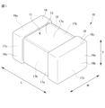
- FIG. 1 shows a multilayer ceramic capacitor 10 as an electronic component applied to a mounting structure for an electronic component according to a first embodiment.
- the first embodiment is one form of a structure in which the multilayer ceramic capacitor 10 is mounted on a substrate.
- the dimensions of the multilayer ceramic capacitor 10 include, for example, a length direction L of 0.2 mm or more and 1.7 mm or less, a width direction W of 0.12 mm or more and 0.9 mm or less, and a stacking direction T of 0.12 mm or more and 0.9 mm or less, but are not limited to these.
- the dielectric layer 121 and the outer dielectric ceramic layer 13 are formed by firing, for example, a ceramic material mainly composed of barium titanate or other ceramic material with a high dielectric constant (e.g., a material mainly composed of CaTiO3 , SrTiO3 , CaZrO3, etc.).
- a ceramic material mainly composed of barium titanate or other ceramic material with a high dielectric constant e.g., a material mainly composed of CaTiO3 , SrTiO3 , CaZrO3, etc.
- the external electrode 16 is composed of, for example, a laminated film of a sintered metal layer and a plating layer.
- the sintered metal layer is formed by baking a paste of, for example, Cu, Ni, Ag, Pd, Ag-Pd alloy, Au, or the like.
- the plating layer is composed of, for example, a Ni plating layer covered by a Sn plating layer.
- the multilayer ceramic capacitor 10 is manufactured, for example, by firing the component body 11 and then forming a pair of external electrodes 16 by baking, plating, or the like. In some cases, a portion of the external electrodes 16 is fired simultaneously with the component body 11, and then a plating layer of the external electrodes 16 is formed.
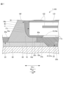
- the mounting structure 1 of the first embodiment will be described with reference to Fig. 2 and Fig. 3. In order to distinguish the mounting structure 1 of the first embodiment from the mounting structure 1 of the other embodiments, the mounting structure 1 of the first embodiment will be referred to as a mounting structure 101. The same applies to the other embodiments.
- the substrate 20 is formed in a sheet shape from an insulating material such as resin, glass, glass epoxy, paper phenol, or ceramics.
- the wiring 33 including the lands 30 is formed by depositing a highly conductive metal such as Cu or Ag on the surface 20a of the substrate 20.
- a highly conductive metal such as Cu or Ag
- Each of the pair of lands 30 has a rectangular shape in a plan view and has approximately the same shape and dimensions as each other.
- the direction perpendicular to the surface 20a of the substrate 20 is referred to as the "Z direction”.
- the direction perpendicular to the Z direction and in which the pair of lands 30 are lined up is referred to as the "X direction”.
- the direction perpendicular to the X direction and the Z direction is referred to as the "Y direction”.
- the direction in which the pair of lands 30 are separated is referred to as the "separating direction X1”
- the direction in which the pair of lands 30 face each other is referred to as the "facing direction X2”.
- “land thickness” refers to the dimension of the land 30 in the Z direction.
- peripheral edges of the pair of lands 30 in the X and Y directions are referred to as the "periphery 31.”
- the edge of the peripheral edge 31 on the separation portion 21 side is referred to as the “inner edge 31a.”
- the inner edge 31a is a straight line extending in the Y direction.
- the end of the land-facing extending portion 16d on the facing direction X2 side is referred to as an extending portion end 16e.
- the extending portion end 16e (boundary portion 15) is located in the separation direction X1 further from the inner edge 31a of the land 30 connected to the land-facing extending portion 16d.
- the end of the land-facing extension 16d in the facing direction X2 is referred to as an extension end 16e.
- the end of the external electrode 16 in the separation direction X1 is referred to as a separation direction end 16f.
- the separation direction end 16f refers to the portion of the end surface 16a of the external electrode 16 in the longitudinal direction L that is located closest to the separation direction X1.
- the thickness of the insulating film 22, the thickness of the land 30, and the thickness of the solder 40 arranged on the land 30 are measured, for example, on a cross section obtained by cutting the mounting structure 101 of the first embodiment parallel to the X and Z directions so as to pass through the center of the multilayer ceramic capacitor 10 in the Y direction.
- the thickness value of the solder 40 is determined, for example, by measuring the thickness of the solder 40 at multiple (e.g., three) positions on the cross section that are equally spaced in the X direction, and averaging the values obtained. The same applies to the insulating film 22 and the land 30.
- an insulating film 22 is placed on the substrate 20.
- the insulating film 22 is placed, for example, so as to cover a portion of the land 30 including the peripheral portion 31.
- a paste-like solder material is applied to the area of the land 30 that is not covered by the insulating film 22.
- the multilayer ceramic capacitor 10 is placed in a predetermined position on the land 30. Then, as the solder material solidifies, the external electrode 16 and the land 30 are connected by the solder 40.
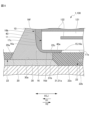
- the mounting structure 103 of the second embodiment differs from the mounting structure 101 of the first embodiment in the position of the opposing end 40a of the solder 40.
- the opposing end 40a is located between the extension end 16e and the separation end 16f in the X direction.
- the insulating film end 22c is located between the extension end 16e and the separation end 16f in the X direction.
- the insulating film end 22c is located at the extension end 16e in the X direction.
- the opposing end 40a is located so as to face the insulating film end 22c in the X direction.
- the provision of the insulating film protrusion 22d more reliably prevents the solder 40 from coming into contact with the component body 11.
- the third embodiment is a partial modification of the first embodiment described above. Therefore, in the reference drawings, the same components as those in the first embodiment are denoted by the same reference numerals, and the description thereof will be omitted. Only the differences will be described.
- the flat extension portion 16g of the land-facing extension portion 16d contacts the land 30 without the solder 40. Between positions D and E, there is no solder 40 between the extension surface 16h and the land surface 30a.
- the opposing end 40a is located on the separation direction X1 side of the portion where the flat portion 16g of the extension portion faces the land 30. This reliably prevents the solder 40 from coming into contact with the component body 11.
- the fourth embodiment is a partial modification of the first embodiment described above. Therefore, in the reference drawings, the same components as those in the first embodiment are denoted by the same reference numerals, and the description thereof will be omitted. Only the differences will be described.
- the mounting structure 105 of the fourth embodiment differs from the mounting structure 101 of the first embodiment in the position of the land 30.
- the upper end of the inner edge 31a of the land 30 is called the land upper end 31b.
- “upper” refers to the direction perpendicular to the surface 20a of the substrate 20 and away from the surface 20a.
- the position of the land upper end 31b in the X direction is indicated by position P.
- the land upper end 31b is located in the opposing direction X2 from the extension end 16e.
- the land upper end 31b is located at the position of the extension end 16e.
- the opposing end 40a can be positioned either between the extension end 16e and the separating end 16f or on the separating end 16f, as in the mounting structure 101 of the first embodiment.
- the insulating film end 22c of the insulating film 22a on the land is placed at the desired position for the opposing end 40a. Then, solder 40 is provided so that the opposing end 40a contacts the insulating film end 22c. This allows the opposing end 40a to be placed at the desired position.
- the distance in the X direction between the land top end 31b and the insulating film end 22c is the insulating film distance on the land.
- the insulating film distance on the land is the length in the X direction of the insulating film 22a on the land.
- the insulating film distance on the land in the mounting structure 105 of the fourth embodiment shown in FIG. 7 is shorter than the insulating film distance on the land in the mounting structure 101 of the first embodiment shown in FIG. 4.
- the length in the X direction of the insulating film 22a on the land is shorter than that in the mounting structure 101 of the first embodiment. Therefore, in the mounting structure 105 of the fourth embodiment, it is possible to suppress variations in the bonding strength between the multilayer ceramic capacitor 10 and the substrate 20 after mounting.
- the mounting structure 106 of the fifth embodiment differs from the mounting structure 101 of the first embodiment and the mounting structure 105 of the fourth embodiment in the position of the land 30.
- the opposing end 40a is unlikely to reach the extension end 16e along the land surface 30a. This is because the land surface 30a only extends as far as the extension end 16e in the separation direction X1. Therefore, the mounting structure 106 of the fifth embodiment makes it easier to prevent the solder 40 from coming into contact with the component body 11.
- the insulating film end 22c of the insulating film 22 is positioned at the desired position of the opposing direction end 40a.
- the opposing direction end 40a is unlikely to advance beyond the insulating film end 22c. Therefore, the mounting structure 106 of the fifth embodiment can more reliably prevent the solder 40 from contacting the component body 11.
- the mounting structure 107 of the sixth embodiment differs from the mounting structure 106 of the fifth embodiment in the presence or absence of an insulating film 22.
- the insulating film 22 (inter-separation insulating film 22b) was arranged in the separation portion 21.
- the insulating film 22 is not arranged in the separation portion 21.
- the portion where the inter-separation insulating film 22b was arranged in the mounting structure 106 of the fifth embodiment is now a gap portion 23.
- the opposing end 40a does not contact the insulating film 22 in the opposing direction X2. Therefore, the solder 40 may wet and spread along the land opposing extension 16d.
- the portion where the solder 40 has wet and spread is called the wet spreading portion 40c.
- the wet spreading portion 40c of the solder 40 is formed near the opposing end 40a.
- the opposing end 40a is located either between the extension end 16e and the separating end 16f or on the separating end 16f. This is because the land upper end 31b is located at a position a predetermined distance away from the extension end 16e in the separating direction X1.
- the mounting structure 107 of the sixth embodiment by arranging the land upper end 31b in a predetermined position, it is possible to prevent the solder 40 from contacting the component body 11 without arranging the insulating film 22 on the inter-separation insulating film 22b. In other words, in the mounting structure 107 of the sixth embodiment, it is possible to prevent the solder 40 from contacting the component body 11 without giving special consideration to the arrangement of the insulating film 22.
- the seventh embodiment is a partial modification of the fifth and sixth embodiments described above. Therefore, in the reference drawings, the same components as those in the fifth and sixth embodiments are denoted by the same reference numerals, and the description thereof will be omitted, and mainly only the differences will be described.
- the mounting structure 108 of the seventh embodiment will be described in comparison with the mounting structure 106 of the fifth embodiment.
- the mounting structure 108 of the seventh embodiment is different from the mounting structure 106 of the fifth embodiment in the length of the insulating film 22 existing from the extension portion end 16e in the separation direction X1.
- the distance in the X direction from the extension end 16e to the insulating film end 22c is the insulating film extension distance.
- the insulating film extension distance in the mounting structure 108 of the seventh embodiment shown in FIG. 10 is shorter than the insulating film extension distance in the mounting structure 106 of the fifth embodiment shown in FIG. 8.
- the insulating film end 22c extends beyond the extension end 16e to the land upper end 31b.
- the insulating film end 22c extends beyond the extension end 16e but only to the point just before reaching the land upper end 31b. Therefore, the insulating film extension distance in the mounting structure 108 of the seventh embodiment is shorter than the insulating film extension distance in the mounting structure 106 of the fifth embodiment.
- the insulating film end 22c is positioned further in the opposing direction X2. Therefore, the opposing direction end 40a is also positioned further in the opposing direction X2. As a result, the distance in the X direction over which the solder 40 contacts the land opposing extension 16d becomes longer.
- the insulating film extension distance from the extension end 16e to the insulating film end 22c is shortened, and the distance from the opposing end 40a to the end surface 17c is lengthened. As a result, the electrical resistance between the external electrode 16 and the land 30 can be reduced.
- the land upper end 31b can be positioned further in the facing direction X2 than in the mounting structure 107 of the sixth embodiment. This is because, in the mounting structure 108 of the seventh embodiment, even if the solder 40 spreads in the facing direction X2 starting from the land upper end 31b, the spreading of the solder 40 is stopped by the inter-separation insulating film 22b before it comes into contact with the component body 11.
- ⁇ 6> An electronic component mounting structure according to any one of ⁇ 1> to ⁇ 5>, having an insulating film placed on the substrate, in which the opposing end of the solder contacts the separating end of the insulating film.
Landscapes
- Engineering & Computer Science (AREA)
- Microelectronics & Electronic Packaging (AREA)
- Power Engineering (AREA)
- Manufacturing & Machinery (AREA)
- Fixed Capacitors And Capacitor Manufacturing Machines (AREA)
Priority Applications (1)
| Application Number | Priority Date | Filing Date | Title |
|---|---|---|---|
| JP2025566237A JPWO2025142038A1 (https=) | 2023-12-27 | 2024-10-16 |
Applications Claiming Priority (2)
| Application Number | Priority Date | Filing Date | Title |
|---|---|---|---|
| JP2023221499 | 2023-12-27 | ||
| JP2023-221499 | 2023-12-27 |
Publications (1)
| Publication Number | Publication Date |
|---|---|
| WO2025142038A1 true WO2025142038A1 (ja) | 2025-07-03 |
Family
ID=96217199
Family Applications (1)
| Application Number | Title | Priority Date | Filing Date |
|---|---|---|---|
| PCT/JP2024/036752 Pending WO2025142038A1 (ja) | 2023-12-27 | 2024-10-16 | 電子部品の実装構造 |
Country Status (2)
| Country | Link |
|---|---|
| JP (1) | JPWO2025142038A1 (https=) |
| WO (1) | WO2025142038A1 (https=) |
Citations (7)
| Publication number | Priority date | Publication date | Assignee | Title |
|---|---|---|---|---|
| JP2000133544A (ja) * | 1998-10-23 | 2000-05-12 | Taiyo Yuden Co Ltd | チップ電子部品 |
| JP2013122939A (ja) * | 2011-12-09 | 2013-06-20 | Sony Corp | 回路基板 |
| JP2016081937A (ja) * | 2014-10-09 | 2016-05-16 | 京セラ株式会社 | 積層型電子部品およびその実装構造体 |
| JP2017059573A (ja) * | 2015-09-14 | 2017-03-23 | 太陽誘電株式会社 | 複合電子部品及びこれを用いた回路基板 |
| WO2017115441A1 (ja) * | 2015-12-28 | 2017-07-06 | オリンパス株式会社 | 実装構造体、撮像装置および内視鏡 |
| US20190103223A1 (en) * | 2017-10-02 | 2019-04-04 | Samsung Electro-Mechanics Co., Ltd. | Multilayer electronic component and board having the same |
| JP2023053630A (ja) * | 2021-10-01 | 2023-04-13 | 株式会社村田製作所 | 電子部品の実装構造 |
-
2024
- 2024-10-16 JP JP2025566237A patent/JPWO2025142038A1/ja active Pending
- 2024-10-16 WO PCT/JP2024/036752 patent/WO2025142038A1/ja active Pending
Patent Citations (7)
| Publication number | Priority date | Publication date | Assignee | Title |
|---|---|---|---|---|
| JP2000133544A (ja) * | 1998-10-23 | 2000-05-12 | Taiyo Yuden Co Ltd | チップ電子部品 |
| JP2013122939A (ja) * | 2011-12-09 | 2013-06-20 | Sony Corp | 回路基板 |
| JP2016081937A (ja) * | 2014-10-09 | 2016-05-16 | 京セラ株式会社 | 積層型電子部品およびその実装構造体 |
| JP2017059573A (ja) * | 2015-09-14 | 2017-03-23 | 太陽誘電株式会社 | 複合電子部品及びこれを用いた回路基板 |
| WO2017115441A1 (ja) * | 2015-12-28 | 2017-07-06 | オリンパス株式会社 | 実装構造体、撮像装置および内視鏡 |
| US20190103223A1 (en) * | 2017-10-02 | 2019-04-04 | Samsung Electro-Mechanics Co., Ltd. | Multilayer electronic component and board having the same |
| JP2023053630A (ja) * | 2021-10-01 | 2023-04-13 | 株式会社村田製作所 | 電子部品の実装構造 |
Also Published As
| Publication number | Publication date |
|---|---|
| JPWO2025142038A1 (https=) | 2025-07-03 |
Similar Documents
| Publication | Publication Date | Title |
|---|---|---|
| KR102448667B1 (ko) | 전자 부품 | |
| US10818431B2 (en) | Electronic component | |
| KR102420683B1 (ko) | 전자 부품 | |
| US10790092B2 (en) | Multilayer ceramic electronic component | |
| US10755859B2 (en) | Electronic component | |
| KR102032759B1 (ko) | 전자 부품 | |
| US20180268998A1 (en) | Electronic component | |
| US20240321521A1 (en) | Electronic component | |
| US10811191B2 (en) | Electronic component | |
| KR102562428B1 (ko) | 적층 세라믹 전자부품 | |
| US10650972B2 (en) | Electronic component | |
| KR20190116138A (ko) | 적층형 커패시터 및 그 실장 기판 | |
| KR100375013B1 (ko) | 적층 세라믹 전자 부품 | |
| CN115938802B (zh) | 电子部件的安装构造 | |
| KR102880983B1 (ko) | 세라믹 전자부품 | |
| WO2025142038A1 (ja) | 電子部品の実装構造 | |
| KR102704717B1 (ko) | 세라믹 커패시터 | |
| JP7792481B2 (ja) | 積層コンデンサ | |
| WO2025099997A1 (ja) | 電子部品の実装構造 | |
| JP7524052B2 (ja) | 電子部品 | |
| US20250132094A1 (en) | Electronic component | |
| JP2018129445A (ja) | 電子部品 | |
| WO2026004128A1 (ja) | 積層セラミック電子部品 | |
| JP2020161548A (ja) | 積層セラミック電子部品 | |
| KR20250038729A (ko) | 전자부품 및 전자부품의 실장 구조 |
Legal Events
| Date | Code | Title | Description |
|---|---|---|---|
| 121 | Ep: the epo has been informed by wipo that ep was designated in this application |
Ref document number: 24911931 Country of ref document: EP Kind code of ref document: A1 |
|
| ENP | Entry into the national phase |
Ref document number: 2025566237 Country of ref document: JP Kind code of ref document: A |