WO2025134752A1 - 半導体パッケージ、電子機器 - Google Patents
半導体パッケージ、電子機器 Download PDFInfo
- Publication number
- WO2025134752A1 WO2025134752A1 PCT/JP2024/042640 JP2024042640W WO2025134752A1 WO 2025134752 A1 WO2025134752 A1 WO 2025134752A1 JP 2024042640 W JP2024042640 W JP 2024042640W WO 2025134752 A1 WO2025134752 A1 WO 2025134752A1
- Authority
- WO
- WIPO (PCT)
- Prior art keywords
- wire
- pad
- imaging element
- element chip
- semiconductor package
- Prior art date
- Legal status (The legal status is an assumption and is not a legal conclusion. Google has not performed a legal analysis and makes no representation as to the accuracy of the status listed.)
- Pending
Links
Images









Classifications
-
- H—ELECTRICITY
- H04—ELECTRIC COMMUNICATION TECHNIQUE
- H04N—PICTORIAL COMMUNICATION, e.g. TELEVISION
- H04N25/00—Circuitry of solid-state image sensors [SSIS]; Control thereof
- H04N25/70—SSIS architectures; Circuits associated therewith
-
- H—ELECTRICITY
- H10—SEMICONDUCTOR DEVICES; ELECTRIC SOLID-STATE DEVICES NOT OTHERWISE PROVIDED FOR
- H10F—INORGANIC SEMICONDUCTOR DEVICES SENSITIVE TO INFRARED RADIATION, LIGHT, ELECTROMAGNETIC RADIATION OF SHORTER WAVELENGTH OR CORPUSCULAR RADIATION
- H10F39/00—Integrated devices, or assemblies of multiple devices, comprising at least one element covered by group H10F30/00, e.g. radiation detectors comprising photodiode arrays
- H10F39/10—Integrated devices
- H10F39/12—Image sensors
-
- H—ELECTRICITY
- H10—SEMICONDUCTOR DEVICES; ELECTRIC SOLID-STATE DEVICES NOT OTHERWISE PROVIDED FOR
- H10W—GENERIC PACKAGES, INTERCONNECTIONS, CONNECTORS OR OTHER CONSTRUCTIONAL DETAILS OF DEVICES COVERED BY CLASS H10
- H10W72/00—Interconnections or connectors in packages
- H10W72/071—Connecting or disconnecting
Definitions
- This technology relates to semiconductor packages and electronic devices, for example, semiconductor packages and electronic devices that can be made smaller.
- a chip such as an image sensor is mounted on a semiconductor mounting substrate and packaged so that the sensor surface of the image sensor is protected by sealing glass.
- the image sensor and the semiconductor mounting substrate are connected by wire wiring formed by wire bonding (see, for example, Patent Document 1).
- the sealing glass and the image sensor are connected by resin. If the width of the resin is reduced to make the semiconductor package smaller, there is a risk that the resin will be crushed by the weight of the sealing glass.
- a first semiconductor package includes an imaging device chip having a first pad, a substrate on which the imaging device chip is mounted and having a second pad, a first wire wiring that connects the first pad to the second pad, the first pads to each other, or the second pads to each other with a metal wire, a second wire wiring that connects the first pad to the second pad with a metal wire, and a resin that is provided around the imaging device chip and bonds a seal glass provided on the light incident surface side of the imaging device chip, the highest point of the first wire wiring being the longest distance from the surface of the imaging device chip is provided at a position closer to the seal glass than the highest point of the second wire wiring, and the highest point of the first wire wiring is a semiconductor package that is encapsulated in the resin.
- a first electronic device includes an imaging device chip having a first pad, a substrate on which the imaging device chip is mounted and having a second pad, a first wire wiring that connects the first pad to the second pad, the first pads to each other, or the second pads to each other with a metal wire, a second wire wiring that connects the first pad to the second pad with a metal wire, and a resin that is provided around the imaging device chip and bonds a seal glass provided on the light incident surface side of the imaging device chip, the highest point of the first wire wiring that is the longest distance from the surface of the imaging device chip is provided at a position closer to the seal glass than the highest point of the second wire wiring, and the highest point of the first wire wiring is an electronic device that includes a semiconductor package that is encapsulated in the resin.
- a second semiconductor package includes an imaging element chip having a first pad, a substrate on which the imaging element chip is mounted and has a second pad, a first wire wiring connected to either the first pad or the second pad, a second wire wiring connecting the first pad and the second pad by a metal wire, and a resin provided around the imaging element chip and bonding a seal glass provided on the light incident surface side of the imaging element chip, the highest point of the first wire wiring being the longest distance from the surface of the imaging element chip is provided at a position closer to the seal glass than the highest point of the second wire wiring, and the highest point of the first wire wiring is a semiconductor package encapsulated in the resin.
- a second electronic device is an electronic device that includes an imaging element chip having a first pad, a substrate on which the imaging element chip is mounted and having a second pad, a first wire wiring connected to either the first pad or the second pad, a second wire wiring connecting the first pad and the second pad by a metal wire, and a resin that is provided around the imaging element chip and bonds a seal glass provided on the light incident surface side of the imaging element chip, the highest point of the first wire wiring being the longest distance from the surface of the imaging element chip is provided at a position closer to the seal glass than the highest point of the second wire wiring, and the highest point of the first wire wiring is an electronic device that includes a semiconductor package encapsulated in the resin.
- a first semiconductor package includes an imaging element chip having a first pad, a substrate on which the imaging element chip is mounted and having a second pad, a first wire wiring that connects the first pad to the second pad, the first pads to each other, or the second pads to each other with a metal wire, a second wire wiring that connects the first pad to the second pad with a metal wire, and a resin that is provided around the imaging element chip and bonds a seal glass provided on the light incident surface side of the imaging element chip.
- the highest point of the first wire wiring which is the longest distance from the surface of the imaging element chip, is provided at a position closer to the seal glass than the highest point of the second wire wiring, and the highest point of the first wire wiring is encapsulated in the resin.
- a first electronic device is provided with the first semiconductor package.
- a second semiconductor package includes an imaging element chip having a first pad, a substrate on which the imaging element chip is mounted and having a second pad, a first wire wiring connected to either the first pad or the second pad, a second wire wiring connecting the first pad and the second pad by a metal wire, and a resin provided around the imaging element chip and bonding a seal glass provided on the light incident surface side of the imaging element chip.
- the highest point of the first wire wiring which is the longest distance from the surface of the imaging element chip, is provided at a position closer to the seal glass than the highest point of the second wire wiring, and the highest point of the first wire wiring is encapsulated in the resin.
- a second electronic device according to one aspect of the present technology is provided with the second semiconductor package.
- FIG. 1 is a diagram showing a configuration of an embodiment of a semiconductor package to which the present technology is applied;
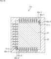
- FIG. 2 is a diagram illustrating an example of a planar configuration of a semiconductor package.
- 11A and 11B are diagrams illustrating another example of a planar configuration of a semiconductor package.
- 11A and 11B are diagrams illustrating another example of a planar configuration of a semiconductor package.
- FIG. 13 is a diagram for explaining differences in height of wire wiring.
- FIG. 13 is a diagram for explaining how to make wire wiring.
- FIG. 13 is a diagram for explaining how to make wire wiring.
- 13 is a diagram illustrating an example of a planar configuration of a semiconductor package according to a second embodiment;
- FIG. 13 is a diagram illustrating an example of a cross-sectional configuration of a semiconductor package according to a second embodiment.
- FIG. 13 is a diagram illustrating an example of a planar configuration of a semiconductor package according to a third embodiment. 13 is a diagram showing an example of a planar configuration of wire wiring according to the third embodiment;
- FIG. 13 is a diagram illustrating an example of a planar configuration of a semiconductor package according to a fourth embodiment.
- FIG. 13 is a diagram illustrating an example of a cross-sectional configuration of a semiconductor package according to a fifth embodiment. 13 is a diagram illustrating another example of a cross-sectional configuration of the semiconductor package according to the fifth embodiment.
- FIG. 13 is a diagram illustrating an example of a cross-sectional configuration of a semiconductor package according to a second embodiment.
- FIG. 13 is a diagram illustrating an example of a planar configuration of a semiconductor package according to a third embodiment. 13 is a diagram showing an example of a planar configuration
- FIG. 23 is a diagram illustrating an example of a cross-sectional configuration of a semiconductor package according to a sixth embodiment.
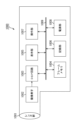
- FIG. 1 is a diagram illustrating an example of the configuration of an electronic device. 1 is a diagram illustrating an example of a schematic configuration of an endoscopic surgery system. 2 is a block diagram showing an example of the functional configuration of a camera head and a CCU.
- FIG. 1 is a block diagram showing an example of a schematic configuration of a vehicle control system; 4 is an explanatory diagram showing an example of the installation positions of an outside-vehicle information detection unit and an imaging unit; FIG.
- Fig. 1 is a diagram showing a cross-sectional configuration example of an embodiment of a semiconductor package to which the present technology is applied
- Fig. 2 is a diagram showing a planar configuration example.
- a semiconductor package 11 described below houses and packages an image sensor chip 21 as an image sensor.
- the semiconductor package 11 shown in FIG. 1 includes an image sensor chip 21, a semiconductor mounting substrate 22, a seal glass 23, a sealing resin 24, a seal glass resin 25, and a die bond resin 26.
- the image sensor chip 21 and the semiconductor mounting substrate 22 are connected by normal wire wiring 31 and high wire wiring 41.
- the normal wire wiring 31 and the high wire wiring 41 each have a curved portion, and the curved portion of the high wire wiring 41 is formed at a higher position than the normal wire wiring, so here it is referred to as the high wire wiring 41 to distinguish it from the normal wire wiring 31.
- the imaging element chip 21 is, for example, an imaging element such as a CCD (Charge Coupled Device) image sensor or a CMOS (Complementary Metal Oxide Semiconductor) image sensor, and has a sensor surface on which multiple pixels are arranged in an array.
- CCD Charge Coupled Device
- CMOS Complementary Metal Oxide Semiconductor
- the semiconductor mounting substrate 22 is a substrate for mounting the imaging element chip 21.
- the semiconductor mounting substrate 22 has multiple layers of wiring stacked inside.
- An insulating film (not shown) such as solder resist is formed on the upper surface of the semiconductor mounting substrate 22, and pads 33 made of a nickel layer or a gold plating layer are provided for joining normal wire wiring 31 or high wire wiring 41.
- An insulating film (not shown) such as solder resist is formed on the lower surface of the semiconductor mounting substrate 22, and a nickel layer or a gold plating layer is provided for joining solder balls (not shown).
- the sealing glass 23 is a glass substrate for protecting the sensor surface of the imaging element chip 21, and is provided on the light incident surface side of the semiconductor package 11.
- the sealing resin 24 is a resin material that is provided to surround the outer periphery of the side surface of the imaging element chip 21 and the sealing glass 23, and is used to seal the normal wire wiring 31 and the high wire wiring 41.
- the sealing resin 24 can be an epoxy-based resin that begins to harden at temperatures of 50°C or higher.
- the sealing glass resin 25 is used to mount the sealing glass 23 to the imaging element chip 21.
- the sealing glass resin 25 may be a mixed resin made by mixing an acrylic system and an epoxy system, which is pre-cured with an ultraviolet amount of 1 J/cm2 or more and starts to thermally cure at 50°C or more, and is cured by ultraviolet light and heat.
- the die-bond resin 26 is used to mount the image sensor chip 21 on the semiconductor mounting substrate 22.
- the die-bond resin 26 may be an acrylic, epoxy, or silicone resin that begins to harden at 50°C or higher.
- solder balls are used when mounting the semiconductor package 11 to an electronic device such as an imaging device, and the solder material may be, for example, a lead-free solder (e.g., Sn-3.0Ag-0.5Cu) with a melting point of approximately 220°C.
- a lead-free solder e.g., Sn-3.0Ag-0.5Cu
- the wire wiring 31 connects a pad 33 provided on the semiconductor mounting substrate 22 to a pad 34 provided on the imaging device chip 21 by a metal wire 32.
- a gold wire with a diameter of 25 ⁇ m is used for the metal wire 32.
- the high wire wiring 41 connects the pad 33 provided on the semiconductor mounting substrate 22 to the pad 34 provided on the imaging element chip 21 by a metal wire 42.
- the metal wire 42 may be made of a gold wire having a diameter of, for example, 25 ⁇ m, the same as the metal wire 32, or it may be made of a gold wire thicker than the metal wire 32.
- the normal wire wiring 31 and the high wire wiring 41 have the same basic configuration and connect the imaging device chip 21 and the semiconductor mounting substrate 22. Although details will be described later, the normal wire wiring 31 and the high wire wiring 41 are both formed in a linear shape and are similar in that they have a partially curved shape, but the difference is that the curved part of the high wire wiring 41 is formed at a higher position than the curved part of the normal wire wiring 31, in other words, at a position closer to the seal glass 23.
- the high wire wiring 41, together with the seal glass resin 25, has the function of supporting the seal glass 23.
- the high wire wiring 41 has the function of supporting the seal glass 23 so that the distance between the image sensor chip 21 and the seal glass 23 does not become smaller than a certain distance, and so that the seal glass resin 25 does not become crushed or deformed, for example, horizontally, due to the weight of the seal glass 23 and does not reach the area where the image sensor of the image sensor chip 21 is located.
- the high wire wiring 41 has the function of supporting the seal glass 23
- a metal wire 42 thicker than the normal wire wiring 31 may be used.
- the metal wire 42 of the high wire wiring 41 is illustrated with a thicker line type than the metal wire 32 of the normal wire wiring 31. This description is for the purpose of explanation, and the present embodiment includes the metal wire 42 of the high wire wiring 41 and the metal wire 32 of the normal wire wiring 31 whether they are formed with the same thickness or different thicknesses.
- one of the multiple normal wire wirings 31 is set as a high wire wiring 41.
- the image sensor chip 21 is disposed in the central region of the semiconductor mounting substrate 22.
- the image sensor chip 21 and the semiconductor mounting substrate 22 are connected by a plurality of normal wire wirings 31.
- the image sensor chip 21 and the semiconductor mounting substrate 22 are each formed in a rectangular shape when viewed in a plan view, with pads 34 provided on three sides of the image sensor chip 21 and pads 33 provided on three sides of the semiconductor mounting substrate 22.
- the normal wire wiring 31 is configured such that a metal wire 32 connects a pad 34 on the imaging element chip 21 to a pad 33 on the semiconductor mounting substrate 22 that is provided at a corresponding position.
- the wiring 31 typically includes wires for outputting signals processed by the image sensor chip 21 to a downstream control unit provided on the semiconductor mounting substrate 22, wires for supplying power supply voltage, and grounded wires.
- one of the three sides on which normal wire wiring 31 is provided is provided as a high wire wiring 41, and one of the multiple normal wire wirings 31 provided on that side is provided as a high wire wiring 41.
- the high wire wiring 41 is surrounded by a square so that it can be distinguished from the normal wire wiring 31.
- the normal wire wiring 31 located approximately in the center of the left side in the figure is formed of a high wire wiring 41.
- the high wire wiring 41 has the function of holding the seal glass 23.
- the applicant has confirmed that the seal glass 23 can be held by providing one high wire wiring 41. Holding the seal glass 23 means that the position of the seal glass 23 is maintained with a small amount of deformation of the seal glass resin 25, the distance between the seal glass 23 and the imaging element chip 21 in the vertical direction being maintained at or above the desired distance, and the width of the seal glass resin 25 in the planar direction not exceeding the desired width.
- the seal glass 23 is held by the seal glass resin 25, but if the width of the seal glass resin 25 in the planar direction is narrowed in order to miniaturize the semiconductor package 11, in other words, if the amount of seal glass resin 25 applied is reduced, the seal glass resin 25 may not be strong enough to hold the seal glass 23 and may deform, resulting in a state in which the seal glass 23 cannot be held.
- the high wire wiring 41 is provided. By providing the high wire wiring 41, the seal glass 23 can be held not only by the seal glass resin 25 but also by the high wire wiring 41, preventing the seal glass resin 25 from deforming and making it possible to hold the seal glass 23 in the appropriate position.
- the high wire wiring 41f included in the semiconductor package 11f shown in FIG. 15 has a shape similar to that of the high wire wiring 41 in the first embodiment shown in FIG. 1, but cut in the middle.
- the input device 11204 is an input interface for the endoscopic surgery system 11000.
- a user can input various information and instructions to the endoscopic surgery system 11000 via the input device 11204.
- the user inputs an instruction to change the imaging conditions (type of irradiation light, magnification, focal length, etc.) of the endoscope 11100.
- the light source device 11203 may be controlled to change the intensity of the light it outputs at predetermined time intervals.
- the image sensor of the camera head 11102 may be controlled to acquire images in a time-division manner in synchronization with the timing of the change in the light intensity, and the images may be synthesized to generate an image with a high dynamic range that is free of so-called blackout and whiteout.
- excitation light is irradiated to body tissue and fluorescence from the body tissue is observed (autofluorescence observation), or a reagent such as indocyanine green (ICG) is locally injected into the body tissue and excitation light corresponding to the fluorescence wavelength of the reagent is irradiated to the body tissue to obtain a fluorescent image.
- the light source device 11203 may be configured to supply narrow band light and/or excitation light corresponding to such special light observation.
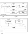
- FIG. 18 is a block diagram showing an example of the functional configuration of the camera head 11102 and CCU 11201 shown in FIG. 17.
- the camera head 11102 has a lens unit 11401, an imaging unit 11402, a drive unit 11403, a communication unit 11404, and a camera head control unit 11405.
- the CCU 11201 has a communication unit 11411, an image processing unit 11412, and a control unit 11413.
- the camera head 11102 and the CCU 11201 are connected to each other via a transmission cable 11400 so that they can communicate with each other.
- the lens unit 11401 is an optical system provided at the connection with the lens barrel 11101. Observation light taken in from the tip of the lens barrel 11101 is guided to the camera head 11102 and enters the lens unit 11401.
- the lens unit 11401 is composed of a combination of multiple lenses including a zoom lens and a focus lens.
- the imaging unit 11402 may include one imaging element (a so-called single-plate type) or multiple imaging elements (a so-called multi-plate type).
- each imaging element may generate an image signal corresponding to each of RGB, and a color image may be obtained by combining these.
- the imaging unit 11402 may be configured to have a pair of imaging elements for acquiring image signals for the right eye and the left eye corresponding to a 3D (dimensional) display. By performing a 3D display, the surgeon 11131 can more accurately grasp the depth of the biological tissue in the surgical site.
- multiple lens units 11401 may be provided corresponding to each imaging element.
- the imaging unit 11402 does not necessarily have to be provided in the camera head 11102.
- the imaging unit 11402 may be provided inside the lens barrel 11101, immediately after the objective lens.
- the driving unit 11403 is composed of an actuator, and moves the zoom lens and focus lens of the lens unit 11401 a predetermined distance along the optical axis under the control of the camera head control unit 11405. This allows the magnification and focus of the image captured by the imaging unit 11402 to be adjusted appropriately.
- the communication unit 11404 is configured with a communication device for transmitting and receiving various information to and from the CCU 11201.
- the communication unit 11404 transmits the image signal obtained from the imaging unit 11402 as RAW data to the CCU 11201 via the transmission cable 11400.
- the above-mentioned frame rate, exposure value, magnification, focus, and other imaging conditions may be appropriately specified by the user, or may be automatically set by the control unit 11413 of the CCU 11201 based on the acquired image signal.
- the endoscope 11100 is equipped with the so-called AE (Auto Exposure) function, AF (Auto Focus) function, and AWB (Auto White Balance) function.
- the camera head control unit 11405 controls the operation of the camera head 11102 based on a control signal from the CCU 11201 received via the communication unit 11404.
- the communication unit 11411 is configured with a communication device for transmitting and receiving various information to and from the camera head 11102.
- the communication unit 11411 receives an image signal transmitted from the camera head 11102 via the transmission cable 11400.
- the communication unit 11411 also transmits to the camera head 11102 a control signal for controlling the operation of the camera head 11102.
- the image signal and the control signal can be transmitted by electrical communication, optical communication, etc.
- the image processing unit 11412 performs various image processing operations on the image signal, which is the RAW data transmitted from the camera head 11102.
- the control unit 11413 performs various controls related to the imaging of the surgical site, etc. by the endoscope 11100, and the display of the captured images obtained by imaging the surgical site, etc. For example, the control unit 11413 generates a control signal for controlling the driving of the camera head 11102.
- the control unit 11413 also causes the display device 11202 to display the captured image showing the surgical site, etc., based on the image signal that has been image-processed by the image processing unit 11412. At this time, the control unit 11413 may recognize various objects in the captured image using various image recognition techniques. For example, the control unit 11413 can recognize surgical tools such as forceps, specific body parts, bleeding, mist generated when the energy treatment tool 11112 is used, etc., by detecting the shape and color of the edges of objects included in the captured image. When the control unit 11413 causes the display device 11202 to display the captured image, it may use the recognition result to superimpose various types of surgical support information on the image of the surgical site. By superimposing the surgical support information and presenting it to the surgeon 11131, the burden on the surgeon 11131 can be reduced and the surgeon 11131 can proceed with the surgery reliably.
- various image recognition techniques such as forceps, specific body parts, bleeding, mist generated when the energy treatment tool 11112 is used, etc.
- the transmission cable 11400 that connects the camera head 11102 and the CCU 11201 is an electrical signal cable that supports electrical signal communication, an optical fiber that supports optical communication, or a composite cable of these.
- communication is performed wired using a transmission cable 11400, but communication between the camera head 11102 and the CCU 11201 may also be performed wirelessly.
- the technology according to the present disclosure can be applied to various products.
- the technology according to the present disclosure may be realized as a device mounted on any type of moving body such as an automobile, an electric vehicle, a hybrid electric vehicle, a motorcycle, a bicycle, a personal mobility device, an airplane, a drone, a ship, or a robot.
- FIG. 19 is a block diagram showing a schematic configuration example of a vehicle control system, which is an example of a mobile object control system to which the technology disclosed herein can be applied.
- the vehicle control system 12000 includes a plurality of electronic control units connected via a communication network 12001.
- the vehicle control system 12000 includes a drive system control unit 12010, a body system control unit 12020, an outside vehicle information detection unit 12030, an inside vehicle information detection unit 12040, and an integrated control unit 12050.
- Also shown as functional components of the integrated control unit 12050 are a microcomputer 12051, an audio/video output unit 12052, and an in-vehicle network I/F (Interface) 12053.
- the drive system control unit 12010 controls the operation of devices related to the drive system of the vehicle according to various programs.
- the drive system control unit 12010 functions as a control device for a drive force generating device for generating the drive force of the vehicle, such as an internal combustion engine or a drive motor, a drive force transmission mechanism for transmitting the drive force to the wheels, a steering mechanism for adjusting the steering angle of the vehicle, and a braking device for generating a braking force for the vehicle.
- the body system control unit 12020 controls the operation of various devices installed in the vehicle body according to various programs.
- the body system control unit 12020 functions as a control device for a keyless entry system, a smart key system, a power window device, or various lamps such as headlamps, tail lamps, brake lamps, turn signals, and fog lamps.
- radio waves or signals from various switches transmitted from a portable device that replaces a key can be input to the body system control unit 12020.
- the body system control unit 12020 accepts the input of these radio waves or signals and controls the vehicle's door lock device, power window device, lamps, etc.
- the outside-vehicle information detection unit 12030 detects information outside the vehicle equipped with the vehicle control system 12000.
- the image capturing unit 12031 is connected to the outside-vehicle information detection unit 12030.
- the outside-vehicle information detection unit 12030 causes the image capturing unit 12031 to capture images outside the vehicle and receives the captured images.
- the outside-vehicle information detection unit 12030 may perform object detection processing or distance detection processing for people, cars, obstacles, signs, characters on the road surface, etc. based on the received images.
- the imaging unit 12031 is an optical sensor that receives light and outputs an electrical signal according to the amount of light received.
- the imaging unit 12031 can output the electrical signal as an image, or as distance measurement information.
- the light received by the imaging unit 12031 may be visible light, or may be invisible light such as infrared light.
- the in-vehicle information detection unit 12040 detects information inside the vehicle.
- a driver state detection unit 12041 that detects the state of the driver is connected.
- the driver state detection unit 12041 includes, for example, a camera that captures an image of the driver, and the in-vehicle information detection unit 12040 may calculate the driver's degree of fatigue or concentration based on the detection information input from the driver state detection unit 12041, or may determine whether the driver is dozing off.
- the microcomputer 12051 can calculate control target values for the driving force generating device, steering mechanism, or braking device based on information inside and outside the vehicle acquired by the outside vehicle information detection unit 12030 or the inside vehicle information detection unit 12040, and output control commands to the drive system control unit 12010.
- the microcomputer 12051 can perform cooperative control aimed at realizing the functions of an ADAS (Advanced Driver Assistance System), including vehicle collision avoidance or impact mitigation, following driving based on the distance between vehicles, maintaining vehicle speed, vehicle collision warning, or vehicle lane departure warning.
- ADAS Advanced Driver Assistance System
- the microcomputer 12051 can also perform cooperative control for the purpose of autonomous driving, which allows the vehicle to travel autonomously without relying on the driver's operation, by controlling the driving force generating device, steering mechanism, braking device, etc. based on information about the surroundings of the vehicle acquired by the outside vehicle information detection unit 12030 or the inside vehicle information detection unit 12040.
- the microcomputer 12051 can also output control commands to the body system control unit 12030 based on information outside the vehicle acquired by the outside information detection unit 12030. For example, the microcomputer 12051 can control the headlamps according to the position of a preceding vehicle or an oncoming vehicle detected by the outside information detection unit 12030, and perform cooperative control aimed at preventing glare, such as switching high beams to low beams.
- the audio/image output unit 12052 transmits at least one output signal of audio and image to an output device capable of visually or audibly notifying the occupants of the vehicle or the outside of the vehicle of information.
- an audio speaker 12061, a display unit 12062, and an instrument panel 12063 are exemplified as output devices.
- the display unit 12062 may include, for example, at least one of an on-board display and a head-up display.
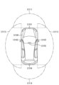
- FIG. 20 shows an example of the installation position of the imaging unit 12031.
- the imaging unit 12031 includes imaging units 12101, 12102, 12103, 12104, and 12105.
- the imaging units 12101, 12102, 12103, 12104, and 12105 are provided, for example, at the front nose, side mirrors, rear bumper, back door, and upper part of the windshield inside the vehicle cabin of the vehicle 12100.
- the imaging unit 12101 provided at the front nose and the imaging unit 12105 provided at the upper part of the windshield inside the vehicle cabin mainly acquire images of the front of the vehicle 12100.
- the imaging units 12102 and 12103 provided at the side mirrors mainly acquire images of the sides of the vehicle 12100.
- the imaging unit 12104 provided at the rear bumper or back door mainly acquires images of the rear of the vehicle 12100.
- the imaging unit 12105 provided at the upper part of the windshield inside the vehicle cabin is mainly used to detect leading vehicles, pedestrians, obstacles, traffic lights, traffic signs, lanes, etc.
- FIG. 20 shows an example of the imaging ranges of the imaging units 12101 to 12104.
- Imaging range 12111 indicates the imaging range of the imaging unit 12101 provided on the front nose
- imaging ranges 12112 and 12113 indicate the imaging ranges of the imaging units 12102 and 12103 provided on the side mirrors, respectively
- imaging range 12114 indicates the imaging range of the imaging unit 12104 provided on the rear bumper or back door.
- an overhead image of the vehicle 12100 viewed from above is obtained by superimposing the image data captured by the imaging units 12101 to 12104.
- the audio/image output unit 12052 controls the display unit 12062 to superimpose a rectangular contour line for emphasis on the recognized pedestrian.
- the audio/image output unit 12052 may also control the display unit 12062 to display an icon or the like indicating a pedestrian at a desired position.
- an imaging element chip having a first pad; a substrate on which the imaging element chip is mounted and which has a second pad; a first wire interconnection that connects the first pad and the second pad, the first pads together, or the second pads together by a metal wire; a second wire interconnection connecting the first pad and the second pad by a metal wire; a resin provided around the imaging element chip and for bonding a seal glass provided on a light incident surface side of the imaging element chip; a maximum point of the first wire that is farthest from a surface of the imaging element chip is located closer to the seal glass than a maximum point of the second wire; An electronic device comprising a semiconductor package, the highest point of the first wire being encapsulated in resin.
- an imaging element chip having a first pad; a substrate on which the imaging element chip is mounted and which has a second pad; a first wire connected to either the first pad or the second pad; a second wire interconnection connecting the first pad and the second pad by a metal wire; a resin provided around the imaging element chip and for bonding a seal glass provided on a light incident surface side of the imaging element chip; a maximum point of the first wire that is farthest from a surface of the imaging element chip is located closer to the seal glass than a maximum point of the second wire; An electronic device comprising a semiconductor package, the highest point of the first wire being encapsulated in resin.
Landscapes
- Engineering & Computer Science (AREA)
- Multimedia (AREA)
- Signal Processing (AREA)
- Solid State Image Pick-Up Elements (AREA)
Abstract
本技術は、半導体パッケージを小型化することができるようにする半導体パッケージ、電子機器に関する。 第1のパッドを有する撮像素子チップと、撮像素子チップが搭載され、第2のパッドを有する基板と、第1のパッドと第2のパッド、第1のパッド同士、または第2のパッド同士を金属ワイヤによって接続する第1のワイヤ配線と、第1のパッドと第2のパッドとを金属ワイヤによって接続する第2のワイヤ配線と、撮像素子チップの周囲に設けられ、撮像素子チップの光入射面側に設けられたシールガラスを接着する樹脂とを備え、撮像素子チップの表面からの距離が最長となる第1のワイヤ配線の最高点は、第2のワイヤ配線の最高点よりもシールガラスに近い位置に設けられ、第1のワイヤ配線の最高点は、樹脂に内包されている。本技術は、例えば、撮像素子を含む半導体パッケージに適用できる。
Description
本技術は半導体パッケージ、電子機器に関し、例えば、小型化できるようにした半導体パッケージ、電子機器に関する。
従来、撮像素子などのチップを半導体搭載基板に搭載し、撮像素子のセンサ面をシールガラスで保護するようにパッケージ化した半導体パッケージでは、撮像素子および半導体搭載基板が、ワイヤボンディングによって形成されるワイヤ配線により接続される(例えば、特許文献1参照)。
半導体パッケージでは、シールガラスと撮像素子とが樹脂により接続されている。半導体パッケージを小型化するために、樹脂の幅を縮小すると、シールガラスの自重で樹脂が潰れてしまう可能性があった。
樹脂が潰れることにより、撮像素子のセンサ面上に樹脂がかかってしまったり、シールガラスとセンサ面との間の距離が所望とされる距離よりも短くなってしまったりする可能性があった。
樹脂が潰れるようなことなく、半導体パッケージを小型化することが望まれている。
本技術は、このような状況に鑑みてなされたものであり、半導体パッケージを小型化することができるようにするものである。
本技術の一側面の第1の半導体パッケージは、第1のパッドを有する撮像素子チップと、前記撮像素子チップが搭載され、第2のパッドを有する基板と、前記第1のパッドと前記第2のパッド、前記第1のパッド同士、または前記第2のパッド同士を金属ワイヤによって接続する第1のワイヤ配線と、前記第1のパッドと前記第2のパッドとを金属ワイヤによって接続する第2のワイヤ配線と、前記撮像素子チップの周囲に設けられ、前記撮像素子チップの光入射面側に設けられたシールガラスを接着する樹脂とを備え、前記撮像素子チップの表面からの距離が最長となる前記第1のワイヤ配線の最高点は、前記第2のワイヤ配線の最高点よりも前記シールガラスに近い位置に設けられ、前記第1のワイヤ配線の前記最高点は、前記樹脂に内包されている半導体パッケージである。
本技術の一側面の第1の電子機器は、第1のパッドを有する撮像素子チップと、前記撮像素子チップが搭載され、第2のパッドを有する基板と、前記第1のパッドと前記第2のパッド、前記第1のパッド同士、または前記第2のパッド同士を金属ワイヤによって接続する第1のワイヤ配線と、前記第1のパッドと前記第2のパッドとを金属ワイヤによって接続する第2のワイヤ配線と、前記撮像素子チップの周囲に設けられ、前記撮像素子チップの光入射面側に設けられたシールガラスを接着する樹脂とを備え、前記撮像素子チップの表面からの距離が最長となる前記第1のワイヤ配線の最高点は、前記第2のワイヤ配線の最高点よりも前記シールガラスに近い位置に設けられ、前記第1のワイヤ配線の前記最高点は、前記樹脂に内包されている半導体パッケージを備える電子機器である。
本技術の一側面の第2の半導体パッケージは、第1のパッドを有する撮像素子チップと、前記撮像素子チップが搭載され、第2のパッドを有する基板と、前記第1のパッドまたは前記第2のパッドのどちらか一方と接続されている第1のワイヤ配線と、前記第1のパッドと前記第2のパッドとを金属ワイヤによって接続する第2のワイヤ配線と、前記撮像素子チップの周囲に設けられ、前記撮像素子チップの光入射面側に設けられたシールガラスを接着する樹脂とを備え、前記撮像素子チップの表面からの距離が最長となる前記第1のワイヤ配線の最高点は、前記第2のワイヤ配線の最高点よりも前記シールガラスに近い位置に設けられ、前記第1のワイヤ配線の前記最高点は、前記樹脂に内包されている半導体パッケージである。
本技術の一側面の第2の電子機器は、第1のパッドを有する撮像素子チップと、撮像素子チップが搭載され、第2のパッドを有する基板と、第1のパッドまたは第2のパッドのどちらか一方と接続されている第1のワイヤ配線と、第1のパッドと第2のパッドとを金属ワイヤによって接続する第2のワイヤ配線と、撮像素子チップの周囲に設けられ、撮像素子チップの光入射面側に設けられたシールガラスを接着する樹脂とを備え、撮像素子チップの表面からの距離が最長となる第1のワイヤ配線の最高点は、第2のワイヤ配線の最高点よりもシールガラスに近い位置に設けられ、第1のワイヤ配線の最高点は、樹脂に内包されている半導体パッケージを備える電子機器である。
本技術の一側面の第1の半導体パッケージにおいては、第1のパッドを有する撮像素子チップと、撮像素子チップが搭載され、第2のパッドを有する基板と、第1のパッドと第2のパッド、第1のパッド同士、または前記第2のパッド同士を金属ワイヤによって接続する第1のワイヤ配線と、第1のパッドと第2のパッドとを金属ワイヤによって接続する第2のワイヤ配線と、撮像素子チップの周囲に設けられ、撮像素子チップの光入射面側に設けられたシールガラスを接着する樹脂とが備えられる。撮像素子チップの表面からの距離が最長となる第1のワイヤ配線の最高点は、第2のワイヤ配線の最高点よりもシールガラスに近い位置に設けられ、第1のワイヤ配線の最高点は、樹脂に内包されている。
本技術の一側面の第1の電子機器においては、前記第1の半導体パッケージが備えられている。
本技術の一側面の第2の半導体パッケージにおいては、第1のパッドを有する撮像素子チップと、撮像素子チップが搭載され、第2のパッドを有する基板と、第1のパッドまたは第2のパッドのどちらか一方と接続されている第1のワイヤ配線と、第1のパッドと第2のパッドとを金属ワイヤによって接続する第2のワイヤ配線と、撮像素子チップの周囲に設けられ、撮像素子チップの光入射面側に設けられたシールガラスを接着する樹脂とが備えられる。撮像素子チップの表面からの距離が最長となる第1のワイヤ配線の最高点は、第2のワイヤ配線の最高点よりもシールガラスに近い位置に設けられ、第1のワイヤ配線の最高点は、樹脂に内包されている。
本技術の一側面の第2の電子機器においては、前記第2の半導体パッケージが備えられている。
以下に、本技術を実施するための形態(以下、実施の形態という)について説明する。
<半導体パッケージの構成例>
図1は本技術を適用した半導体パッケージの一実施の形態の断面構成例を示す図であり、図2は、平面構成例を示す図である。以下に説明する半導体パッケージ11は、イメージセンサとしての撮像素子チップ21を収納してパッケージングしている。
図1は本技術を適用した半導体パッケージの一実施の形態の断面構成例を示す図であり、図2は、平面構成例を示す図である。以下に説明する半導体パッケージ11は、イメージセンサとしての撮像素子チップ21を収納してパッケージングしている。
図1に示す半導体パッケージ11は、撮像素子チップ21、半導体搭載基板22、シールガラス23、封止樹脂24、シールガラス樹脂25、ダイボンド樹脂26を備えている。半導体パッケージ11では、撮像素子チップ21および半導体搭載基板22が通常ワイヤ配線31および高ワイヤ配線41によって接続される。
詳細は後述するが、通常ワイヤ配線31と高ワイヤ配線41はそれぞれ湾曲部分を有し、その湾曲部分は、高ワイヤ配線41の方が、通常ワイヤ配線よりも高い位置に形成されているため、ここでは高ワイヤ配線41と記述し、通常ワイヤ配線31と区別する。
撮像素子チップ21は、例えば、CCD(Charge Coupled Device)イメージセンサやCMOS(Complementary Metal Oxide Semiconductor)イメージセンサなどの撮像素子であり、複数の画素がアレイ状に配置されたセンサ面を有する。
半導体搭載基板22は、撮像素子チップ21を搭載するための基板である。半導体搭載基板22は、複数層の配線が内部に積層された構成とされている。半導体搭載基板22の上面側には、ソルダーレジストなどの絶縁膜(不図示)が成膜されているとともに、通常ワイヤ配線31または高ワイヤ配線41を接合するためのニッケル層や金メッキ層からなるパッド33が設けられる。半導体搭載基板22の下面側には、ソルダーレジストなどの絶縁膜(不図示)が成膜されるとともに、はんだボール(不図示)を接合するためのニッケル層や金メッキ層が設けられている。
シールガラス23は、撮像素子チップ21のセンサ面を保護するためのガラス基板であり、半導体パッケージ11の光入射面側に設けられている。
封止樹脂24は、撮像素子チップ21およびシールガラス23の側面の外周を囲うように設けられ、通常ワイヤ配線31と高ワイヤ配線41を封止するための樹脂部材である。例えば、封止樹脂24としては、50℃度以上で硬化を開始するエポキシ系の樹脂を採用することができる。
シールガラス樹脂25は、撮像素子チップ21に対してシールガラス23を実装するのに用いられる。例えば、シールガラス樹脂25としては、紫外線量1J/cm2以上で仮硬化し、50℃以上で熱硬化を開始するようなアクリル系とエポキシ系とを混合した混合樹脂を採用することができ、紫外線および熱により硬化を実施する。
ダイボンド樹脂26は、半導体搭載基板22に対して撮像素子チップ21を実装するのに用いられる。例えば、ダイボンド樹脂26としては、50℃度以上で硬化を開始するアクリル系、エポキシ系、またはシリコーン系の樹脂を採用することができる。
はんだボール(不図示)は、半導体パッケージ11を撮像装置などの電子機器に実装する際に利用され、はんだ材としては、例えば、融点が約220℃である鉛フリーハンダ(例えば、Sn-3.0Ag-0.5Cu)を採用することができる。
通常ワイヤ配線31は、金属ワイヤ32によって、半導体搭載基板22に設けられたパッド33と撮像素子チップ21に設けられたパッド34とを接続する。金属ワイヤ32には、例えば、直径25μmの金線が用いられる。
高ワイヤ配線41は、金属ワイヤ42によって、半導体搭載基板22に設けられたパッド33と撮像素子チップ21に設けられたパッド34とを接続する。金属ワイヤ42には、金属ワイヤ32と同じ例えば、直径25μmの金線が用いられるようにしても良いし、金属ワイヤ32よりも太い金線が用いられるようにすることもできる。
通常ワイヤ配線31と高ワイヤ配線41は、基本的な構成は同じであり、撮像素子チップ21と半導体搭載基板22を接続する。詳細は後述するが、通常ワイヤ配線31と高ワイヤ配線41は共に線状で形成され、一部が湾曲する形状を有している点は同様であるが、高ワイヤ配線41の湾曲した形状の部分は、通常ワイヤ配線31の湾曲した形状の部分よりも高い位置、換言すれば、シールガラス23に近い位置に形成されている点が異なる。
高ワイヤ配線41は、シールガラス樹脂25とともに、シールガラス23を支える機能を有している。高ワイヤ配線41は、撮像素子チップ21とシールガラス23との間の距離が一定の距離以下にならないように、またシールガラス樹脂25がシールガラス23の重みで潰れ、変形、例えば横方向に変形し、撮像素子チップ21の撮像素子が設けられている領域に係るようなことがないようにシールガラス23を支える機能を有する。
高ワイヤ配線41は、シールガラス23を支える機能を有するため、通常ワイヤ配線31よりも太い金属ワイヤ42が用いられるようにしても良い。なお、以下の説明においては、高ワイヤ配線41と通常ワイヤ配線31を区別するために、高ワイヤ配線41の金属ワイヤ42は、通常ワイヤ配線31の金属ワイヤ32よりも太い線種で図示している。このような記載は、説明のためであり、高ワイヤ配線41の金属ワイヤ42と通常ワイヤ配線31の金属ワイヤ32は、同じ太さで形成されていても、異なる太さで形成されていても本実施の形態に含まれる。
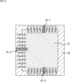
図2に示すように、例えば、複数の通常ワイヤ配線31のうちの1箇所が高ワイヤ配線41とされる。
図2に示した半導体パッケージ11の平面構成例においては、半導体搭載基板22の中央領域に撮像素子チップ21が配置されている。撮像素子チップ21と半導体搭載基板22は、複数の通常ワイヤ配線31で接続されている。
図2に示した例では、平面視において撮像素子チップ21と半導体搭載基板22がそれぞれ四角形状で形成され、撮像素子チップ21の3辺にパッド34が設けられ、半導体搭載基板22の3辺にパッド33が設けられている。
通常ワイヤ配線31は、金属ワイヤ32により撮像素子チップ21のパッド34と、対応する位置に設けられている半導体搭載基板22のパッド33が接続された構成とされている。
通常ワイヤ配線31には、撮像素子チップ21で処理された信号等を、半導体搭載基板22に設けられた後段の制御部などに出力するためワイヤや、電源電圧を供給するワイヤや、接地されているワイヤなどが含まれる。
図2に示した例では、通常ワイヤ配線31が設けられている3辺のうちの1辺に、またその1辺に設けられている複数の通常ワイヤ配線31のうちの1本が、高ワイヤ配線41として設けられている例を示した。説明のため、高ワイヤ配線41は四角で囲み、通常ワイヤ配線31と区別が付くように図示し説明を続ける。図2に示した例では、図中左側の1辺の略中央に位置する通常ワイヤ配線31は、高ワイヤ配線41で形成されている。
高ワイヤ配線41は、シールガラス23を保持する機能を有する。本出願人は、高ワイヤ配線41を1箇所設けることで、シールガラス23を保持できることを確認している。シールガラス23を保持するとは、シールガラス樹脂25の変形量が少なく、垂直方向においてシールガラス23と撮像素子チップ21との距離が所望とされている距離以上保たれ、平面方向においてシールガラス樹脂25の幅が所望とされる幅以上にならない状態で、シールガラス23の位置が保たれることを意味する。
シールガラス23は、シールガラス樹脂25により保持されるが、例えば、半導体パッケージ11を小型化するために、シールガラス樹脂25の平面方向における幅を狭くした場合、換言すれば、シールガラス樹脂25の塗布量が少なくなった場合、シールガラス23を保持するのに十分な強度を保てずにシールガラス樹脂25が変形してしまい、シールガラス23を保持できない状態となる可能性がある。そのようなことを防ぐために、高ワイヤ配線41は設けられている。高ワイヤ配線41を設けることで、シールガラス樹脂25だけではなく、高ワイヤ配線41でもシールガラス23を保持できるようになり、シールガラス樹脂25が変形するようなことを防ぎ、シールガラス23を適切な位置で保持できるようになる。
高ワイヤ配線41が一箇所だけでもシールガラス23を適切に保持できるが、1箇所だけだと、シールガラス23が傾いてしまう可能性がある。図3に示したように、高ワイヤ配線41を3箇所設けるようにしても良い。図3に示した例では、撮像素子チップ21の図中上辺に高ワイヤ配線41-1が配置され、撮像素子チップ21の図中左辺に高ワイヤ配線41-2が配置され、撮像素子チップ21の図中下辺に高ワイヤ配線41-3が配置されている。このように、3箇所に高ワイヤ配線41を設けることで、より確実に、シールガラス23を保持し、シールガラス23が傾くようなことがないように保持することができる。
図示はしていないが、撮像素子チップ21の対向する位置にある2辺に、それぞれ高ワイヤ配線41が設けられている、換言すれば2箇所設けられている構成とすることもできる。
図4に示すように、4辺に、高ワイヤ配線41が設けられている構成としても良い。図4を参照するに、撮像素子チップ21の4辺に、それぞれ高ワイヤ配線41が配置されている。図4に示した例では、撮像素子チップ21の図中上辺に高ワイヤ配線41-1が配置され、撮像素子チップ21の図中左辺に高ワイヤ配線41-2が配置され、撮像素子チップ21の図中下辺に高ワイヤ配線41-3が配置され、撮像素子チップ21の図中右辺に高ワイヤ配線41-4が配置されている。
高ワイヤ配線41-4が設けられている辺には、通常ワイヤ配線31は設けられていない。このように通常ワイヤ配線31が設けられていない辺に、高ワイヤ配線41を配置する構成とすることも可能である。
上記した実施の形態においては、1辺に1つの高ワイヤ配線41が配置されている例を示したが、1辺に2以上の高ワイヤ配線41が配置されているようにしても良い。
<通常ワイヤ配線31と高ワイヤ配線41との比較>
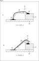
図5は、通常ワイヤ配線31と高ワイヤ配線41の高さの違いについて説明するための図である。図5の左図は、高ワイヤ配線41の部分を拡大した断面図であり、図5の右図は、通常ワイヤ配線31の部分を拡大した断面図である。図5では、封止樹脂24(図1)は図示していない。図5に示したように封止樹脂24を備えない半導体パッケージ11に対しても本技術を適用することはできる。
図5は、通常ワイヤ配線31と高ワイヤ配線41の高さの違いについて説明するための図である。図5の左図は、高ワイヤ配線41の部分を拡大した断面図であり、図5の右図は、通常ワイヤ配線31の部分を拡大した断面図である。図5では、封止樹脂24(図1)は図示していない。図5に示したように封止樹脂24を備えない半導体パッケージ11に対しても本技術を適用することはできる。
図5の右図を参照するに、通常ワイヤ配線31の金属ワイヤ32の一方は、撮像素子チップ21に設けられているパッド34と接続され、他方は、半導体搭載基板22に設けられているパッド33と接続されている。通常ワイヤ配線31の金属ワイヤ32は、線状のワイヤであり、横から見た場合、湾曲した部分がある形状で形成されている。金属ワイヤ32の湾曲した部分は、シールガラス樹脂25外に位置している。図5では図示していない封止樹脂24に、金属ワイヤ32の湾曲した部分が内包されている構成としても良い。
図5の左図を参照するに、高ワイヤ配線41の金属ワイヤ42の一方は、撮像素子チップ21に設けられているパッド34と接続され、他方は、半導体搭載基板22に設けられているパッド33と接続されている。高ワイヤ配線41の金属ワイヤ42は、線状のワイヤであり、横から見た場合、湾曲した部分がある形状で形成されている。金属ワイヤ42の湾曲した部分は、シールガラス樹脂25内に位置し、シールガラス樹脂25内に内包されている。
通常ワイヤ配線31の湾曲部分の最高点の位置を位置P1とし、高ワイヤ配線41の湾曲部分の最高点の位置を位置P2とする。最高点の高さは、例えば、撮像素子チップ21とシールガラス樹脂25との界面を基準とした高さとすることができる。最高点は、基準となる位置から距離が最長となる位置とすることができる。位置P1と位置P2との差分は差分aとなる。すなわち、通常ワイヤ配線31の湾曲部分の最高点の位置よりも差分aだけ高い位置に、高ワイヤ配線41の湾曲部分の最高点がある。
図5の右図では、通常ワイヤ配線31の湾曲部分は、シールガラス樹脂25外に位置している例を示しているが、シールガラス樹脂25に内包されている形状であっても良い。通常ワイヤ配線31の湾曲部分が、シールガラス樹脂25に内包されている形状であっても、通常ワイヤ配線31の湾曲部分の最高点の位置よりも差分aだけ高い位置に、高ワイヤ配線41の湾曲部分の最高点があるという関係が満たされるように、通常ワイヤ配線31と高ワイヤ配線41は、それぞれ形成されている。
高ワイヤ配線41は、通常ワイヤ配線31よりも最高点が高くなるように形成されている。高ワイヤ配線41の湾曲部分、換言すれば、高ワイヤ配線41の最高点を含む所定の範囲内の金属ワイヤ42は、シールガラス23と一部接触する部分がある、またはシールガラス23と所定の距離だけ離れた位置となるような高さまで形成されている。高ワイヤ配線41の湾曲部分(最高点)とシールガラス23との距離bは、例えば、高ワイヤ配線41の金属ワイヤ42の太さと同程度または太さ以下に該当する長さである。
高ワイヤ配線41がシールガラス23と接触するか否かは、シールガラス23の大きさ(重さ)や、シールガラス樹脂25を設ける幅(量)や、シールガラス樹脂25の材料などに依存する。高ワイヤ配線41を設けることで、シールガラス23をシールガラス樹脂25だけでなく、高ワイヤ配線41でも保持することができるようになる。
高ワイヤ配線41は、シールガラス23と接触する可能性があるが、通常ワイヤ配線31は、シールガラス23とは接触しないような高さ、形状で形成されている。通常ワイヤ配線31がシールガラス23と接触すると、通常ワイヤ配線31を介して信号にノイズが載る可能性があるため、このようなことを防ぐために、通常ワイヤ配線31は、シールガラス23と接触することがないように構成されている。また、高ワイヤ配線41を設けることで、シールガラス樹脂25を所望の位置で固定することができるため、通常ワイヤ配線31が、シールガラス23と接触するようなことをより確実に防ぐことが可能となる。
通常ワイヤ配線31は、ノイズが載らないように構成されているため、撮像素子チップ21で処理された信号等を、半導体搭載基板22に設けられた後段の制御部などに出力するためワイヤや、電源電圧を供給するワイヤや、接地されているワイヤなどとして用いられる。高ワイヤ配線41は、シールガラス23と接触する可能性があるため、電源電圧を供給するワイヤや、接地されているワイヤ、またはダミー配線として設けられる。ダミー配線とは、信号や電源電圧を供給しない線である。また、高ワイヤ配線41がダミー配線として設けられている場合、ダミー配線と接続されているパッド33やパッド34も、信号や電源電圧が供給されないダミーパッドとして設けられている。
高ワイヤ配線41をダミー配線とした場合、1つのパッド33に、通常ワイヤ配線31と高ワイヤ配線41の両方が接続されている構成とすることもできる。
シールガラス樹脂25は、撮像素子チップ21を封止する機能と、シールガラス23を保持する機能を有している。高ワイヤ配線41を設けることで、シールガラス23を保持する機能を、高ワイヤ配線41にも持たせることができるため、シールガラス樹脂25自体は、シールガラス23を保持する機能が弱くなっても良くなる。例えば、シールガラス樹脂25は、撮像素子チップ21を封止する機能に特化した材料や、半導体パッケージ11内で発生した熱を外部に放出する熱伝導性が高い材料を用いたりすることができ、シールガラス樹脂25の材料の選択肢を広げることができる。
<通常ワイヤ配線31と高ワイヤ配線41の形成の仕方について>
図6を参照して通常ワイヤ配線31と高ワイヤ配線41の形成の仕方について説明を加える。
図6を参照して通常ワイヤ配線31と高ワイヤ配線41の形成の仕方について説明を加える。
通常ワイヤ配線31は、図6のAに示すように、リバースボンドと称される方法でボンディングすることで形成することができる。リバースボンドで通常ワイヤ配線31を形成する場合、ノズルから所定の太さの金線が排出され、スパークで先端が溶融され、半導体搭載基板22のパッド33上にボールが形成される(1stボンドが作成される)。
ボールがパッド33に圧着されると、撮像素子チップ21と金線が接触しないように、ループ(湾曲部分に該当)が形成される。撮像素子チップ21のパッド34に、金線が圧着され、切断される(2ndボンドが作成される)。
リバースボンドで通常ワイヤ配線31を形成した場合、図6のAに示したように、撮像素子チップ21のセンサ面(表面とする)からの高さが高さcの位置に、ループ(湾曲部分)が来るような金属ワイヤ32を有する通常ワイヤ配線31を形成することができる。
高ワイヤ配線41は、図6のBに示すように、ノーマルボンドと称される方法でボンディングすることで形成することができる。ノーマルボンドで高ワイヤ配線41を形成する場合、ノズルから所定の太さの金線が排出され、スパークで先端が溶融され、撮像素子チップ21のパッド34上にボールが形成される(1stボンドが作成される)。
ボールがパッド34に圧着されると、撮像素子チップ21と金線が接触しないように、ループ(湾曲部分に該当)が形成される。このとき金線が引き上げられることで、撮像素子チップ21の表面から高さdの位置にループ(湾曲部分)が位置するように加工することができる。
ループ形成後、半導体搭載基板22のパッド33に、金線が圧着され、切断される(2ndボンドが形成される)。ノーマルボンドで高ワイヤ配線41を形成した場合、図6のBに示したように、撮像素子チップ21の表面からの高さが高さd(高さd>高さcを満たす)の位置に、ループ(湾曲部分)が来るような金属ワイヤ32を有する高ワイヤ配線41を形成することができる。
このように、ワイヤ配線の形成時に、リバースボンドとノーマルボンドを使い分けることで、通常ワイヤ配線31と高ワイヤ配線41をそれぞれ形成することができる。
ここで例示した形成の仕方は一例であり、他の方法で、通常ワイヤ配線31や高ワイヤ配線41が形成されてもよい。例えば通常ワイヤ配線31を、ノーマルボンドで高さcとなるように形成し、高ワイヤ配線41をリバースボンドで高さdとなるように形成するようにしても良い。例えば、通常ワイヤ配線31と高ワイヤ配線41の両方をリバースボンドまたはノーマルボンドのどちらかで形成し、形成時に、ループの高さが異なるように形成されるようにしても良い。
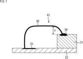
高ワイヤ配線41の形状は、例えば、図7に示すような形状であっても良い。図7に示した高ワイヤ配線41の形状は、最高点が水平(平坦)となっている。図7に示した高ワイヤ配線41の形状は、パッド33側から引き出されている金属ワイヤ42が直線形状から曲線形状になり、その曲線形状の部分が最高点に達した位置から水平方向に、最高点の位置を保ちながら延び、撮像素子チップ21のパッド34付近で曲線形状になり、パッド34と接続されている形状である。
撮像素子チップ21のパッド34付近での曲線形状の一部または全ては、シールガラス樹脂25(図7では不図示)に内包されている。
例えばノーマルボンドを適用することで、様々なループ形状を形成することが可能であり、例えば図7に示したように、最高点となる部分が、直線形状になり、半導体搭載基板22の表面と平行となる直線を有する高ワイヤ配線41を形成することもできる。
<第2の実施の形態>
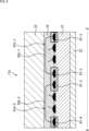
図8は、第2の実施の形態における半導体パッケージ11bの平面構成例を示し、図9は、図8の線分A-A’における半導体パッケージ11bの断面構成例を示す。第1の実施の形態における半導体パッケージ11と同一の部分には、同一の符号を付し、適宜その説明は省略する。
図8は、第2の実施の形態における半導体パッケージ11bの平面構成例を示し、図9は、図8の線分A-A’における半導体パッケージ11bの断面構成例を示す。第1の実施の形態における半導体パッケージ11と同一の部分には、同一の符号を付し、適宜その説明は省略する。
図8、図9に示した半導体パッケージ11bは、撮像素子チップ21の2辺にそれぞれ高ワイヤ配線41bが設けられている。撮像素子チップ21の図中上辺には、高ワイヤ配線41b-1と高ワイヤ配線41b-2が設けられ、撮像素子チップ21の図中下辺には、高ワイヤ配線41b-1’と高ワイヤ配線41b-2’が設けられている。
撮像素子チップ21の図中上辺に設けられている高ワイヤ配線41b-1は、撮像素子チップ21に設けられているパッド61-1とパッド61-2と、パッド61-1とパッド61-2間に配線されている金属ワイヤ42b-1とを含む構成とされている。高ワイヤ配線41b-2は、撮像素子チップ21に設けられているパッド61-3とパッド61-3と、パッド61-3とパッド61-4間に配線されている金属ワイヤ42b-2とを含む構成とされている。
パッド61-1とパッド61-4は、撮像素子チップ21の1辺の両端に設けられ、パッド61-2とパッド61-3は、撮像素子チップ21の1辺の略中央に設けられている。図8に示したように、パッド61-2とパッド61-3を1つのパッドとして形成し、そのパッドの両端に金属ワイヤ42b-1と金属ワイヤ42b-2がそれぞれ接続されるように構成しても良い。この場合、パッド61-2とパッド61-3を含む1つのパッドで形成されたパッドは、パッド61-1やパッド61-2よりも大きく形成されているようにしても良い。
図9に示したように、パッド61-2とパッド61-3をそれぞれ別のパッドとして形成し、金属ワイヤ42b-1と金属ワイヤ42b-2がそれぞれのパッドに接続されるように構成しても良い。この場合、パッド61-2とパッド61-3のそれぞれは、パッド61-1やパッド61-2と同程度の大きさで形成されているようにすることができる。
パッド61-1から61-4までは、全て撮像素子チップ21に設けられている。第2の実施の形態における半導体パッケージ11bにおいては、撮像素子チップ21上に設けられているパッド61同士を金属ワイヤ42bで接続することで高ワイヤ配線41bが形成されている。
図9に示したように、高ワイヤ配線41b-1,41b-2の金属ワイヤ42b-1,42b-2は、撮像素子チップ21の表面と平行となり、直線状に形成され、その部分が最高点となる形状で形成されている。金属ワイヤ42bは、通常ワイヤ配線31と接することがないように、複数の通常ワイヤ配線31上を跨ぐような形状で形成されている。
高ワイヤ配線41bは、シールガラス樹脂25に内包されている。このような形状の高ワイヤ配線41bは、例えば、図7を参照して説明したノーマルボンドを適用して形成することができる。
同様に、撮像素子チップ21の図中下辺には、パッド61-1’から61-4’が設けられている。パッド61-1’とパッド61-2’を接続する金属ワイヤ42b-1’を含む高ワイヤ配線41b-1’と、パッド61-3’とパッド61-4’を接続する金属ワイヤ42b-2’を含む高ワイヤ配線41b-2’が設けられている。
図8に示した例では、撮像素子チップ21の2辺に、それぞれ高ワイヤ配線41bが配置されている例を示したが、撮像素子チップ21の3辺または4辺に、それぞれ高ワイヤ配線41bが配置されている構成とすることもできる。
図8に示した例では、撮像素子チップ21の上辺に高ワイヤ配線41b-1と高ワイヤ配線41b-2が配置され、下辺に高ワイヤ配線41b-1’と高ワイヤ配線41b-2’が配置されている例を示したが、これら4つの高ワイヤ配線41bのうちの2つ、例えば、高ワイヤ配線41b-1と高ワイヤ配線41b-2’が配置されている構成とすることもできる。
高ワイヤ配線41b-1と高ワイヤ配線41b-2を1つの高ワイヤ配線41bとして設ける、換言すれば、パッド61-1とパッド61-4を接続する金属ワイヤ42bから構成される高ワイヤ配線41bが設けられた構成としても良い。
ここでは、1辺に高ワイヤ配線41b-1と高ワイヤ配線41b-2の2本のワイヤ配線が形成されている例を示したが、1辺に2以上の高ワイヤ配線41bが形成されているようにしても良い。
第1の実施の形態と同じく、第2の実施の形態においても、高ワイヤ配線41bでシールガラス23を保持することができ、シールガラス樹脂25の変形量を所定の範囲内に抑えることができ、半導体パッケージ11を小型化することができる。
さらに、高ワイヤ配線41bを基準電源電圧、例えばグランド(GND)に接続することで、ノイズを抑制することもできる。パッド61-1から61-4のそれぞれをGNDに接続することで、GND同士が繋がるGNDループが形成されるため、ノイズを抑制する効果を得ることができる。
<第3の実施の形態>
図10は、第3の実施の形態における半導体パッケージ11cの平面構成例を示し、図11は、図10に示した高ワイヤ配線41c-1の部分を拡大した図である。第1の実施の形態における半導体パッケージ11と同一の部分には、同一の符号を付し、適宜その説明は省略する。
図10は、第3の実施の形態における半導体パッケージ11cの平面構成例を示し、図11は、図10に示した高ワイヤ配線41c-1の部分を拡大した図である。第1の実施の形態における半導体パッケージ11と同一の部分には、同一の符号を付し、適宜その説明は省略する。
図10に示した半導体パッケージ11cは、撮像素子チップ21の2隅にそれぞれ高ワイヤ配線41cが設けられている。撮像素子チップ21の図中右上の隅に設けられている高ワイヤ配線41c-1は、撮像素子チップ21にL字形状で設けられているパッド71-1に配線されている金属ワイヤ42c-1と金属ワイヤ42c-2を含む構成とされている。
図11に示すように、パッド71-1は、撮像素子チップ21の隅に設けられ、その隅の形状に合わせて、L字形状で形成されている。パッド71-1の横方向の辺には金属ワイヤ42c-1が接続され、パッド71-2の横方向の辺には金属ワイヤ42c-2が接続されている。
高ワイヤ配線41c-1のパッド71-1は、L字形状に一体型で形成され、金属ワイヤ42cは、分離した2本の金属ワイヤ42cがL字形状となるように配置されて形成されている。
第3の実施の形態における半導体パッケージ11cにおいては、撮像素子チップ21上に設けられているパッド71に金属ワイヤ42cを接続することで高ワイヤ配線41cが形成されている。
図示はしていないが、第3の実施の形態おける高ワイヤ配線41c-1の金属ワイヤ42c-1,42c-2は、図9に示した金属ワイヤ42b-1,42b-2と同じく、撮像素子チップ21のセンサ面(表面)と平行となり、直線状に形成され、その部分が最高点となる形状で形成されている。また、高ワイヤ配線41cは、シールガラス樹脂25に内包されている。このような形状の高ワイヤ配線41cは、例えば、図7を参照して説明したノーマルボンドを適用して形成することができる。
同様に、撮像素子チップ21の図中左下の隅には、L字形状で形成されたパッド71-2が設けられ、そのL字形状のパッド71-2の一端と中央部分とを接続する金属ワイヤ42c-1’と、パッド71-2の他端と中央部分とを接続する金属ワイヤ42c-2’を含む高ワイヤ配線41c-2が設けられている。
図10に示した例では、撮像素子チップ21の2隅に、それぞれ高ワイヤ配線41cが配置されている例を示したが、撮像素子チップ21の3隅または4隅に、それぞれ高ワイヤ配線41cが配置されている構成とすることもできる。
第1の実施の形態と同じく、第3の実施の形態においても、高ワイヤ配線41cでシールガラス23を保持することができ、シールガラス樹脂25の変形量を所定の範囲内に抑えることができ、半導体パッケージ11を小型化することができる。
<第4の実施の形態>
図12は、第4の実施の形態における半導体パッケージ11dの平面構成例を示す図である。第1の実施の形態における半導体パッケージ11と同一の部分には、同一の符号を付し、適宜その説明は省略する。
図12は、第4の実施の形態における半導体パッケージ11dの平面構成例を示す図である。第1の実施の形態における半導体パッケージ11と同一の部分には、同一の符号を付し、適宜その説明は省略する。
図12は、半導体パッケージ11dの隅の部分を拡大した図である。図12に示した半導体パッケージ11dに含まれる高ワイヤ配線41dは、半導体搭載基板22上に設けられているパッド33同士を接続する。
図12に示した半導体搭載基板22の隅には、パッド33d-1とパッド33d-2が設けられている。パッド33d-1とパッド33d-2が金属ワイヤ42dで接続されることで、高ワイヤ配線41が形成されている。
図示はしていないが高ワイヤ配線41dは、図9に示した金属ワイヤ42b-1,42b-2と同じく、撮像素子チップ21のセンサ面(表面)と平行となり、直線状に形成され、その部分が最高点となる形状で形成されている。また、高ワイヤ配線41d(金属ワイヤ42d)の一部、具体的には、撮像素子チップ21上に位置している高ワイヤ配線41d(金属ワイヤ42d)は、シールガラス樹脂25に内包されている。このような形状の高ワイヤ配線41dは、例えば、図7を参照して説明したノーマルボンドを適用して形成することができる。
高ワイヤ配線41dは、半導体搭載基板22の1隅、2隅、3隅、または4隅に配置されている構成とすることができる。
第1の実施の形態と同じく、第4の実施の形態においても、高ワイヤ配線41dでシールガラス23を保持することができ、シールガラス樹脂25の変形量を所定の範囲内に抑えることができ、半導体パッケージ11を小型化することができる。
<第5の実施の形態>
図13は、第4の実施の形態における半導体パッケージ11eの断面構成例を示す図である。第1の実施の形態における半導体パッケージ11と同一の部分には、同一の符号を付し、適宜その説明は省略する。
図13は、第4の実施の形態における半導体パッケージ11eの断面構成例を示す図である。第1の実施の形態における半導体パッケージ11と同一の部分には、同一の符号を付し、適宜その説明は省略する。
図13に示した半導体パッケージ11eに含まれる高ワイヤ配線41eは、パッド34から垂直方向に直線形状を有する金属ワイヤ42eで形成されている。高ワイヤ配線41eは、撮像素子チップ21上に設けられている1つのパッド34に接続されている。
上述した第1から第3の実施の形態における高ワイヤ配線41は、2つのパッドに接続されている構成例を示したが、第4の実施の形態における高ワイヤ配線41eは、1つのパッド34に接続されている。よって、図13では図示しているが、高ワイヤ配線41の金属ワイヤ42eを接続する半導体搭載基板22上にパッド33は、設けない構成とすることも可能である。
高ワイヤ配線41eは、図14に示すように、湾曲した形状であり、バネ形状に形成された金属ワイヤ42e’を含む構成とすることも可能である。金属ワイヤ42e’をバネ形状にすることで、シールガラス樹脂25の重みを吸収し、より確実に保持することができる高ワイヤ配線41e’とすることができる。
高ワイヤ配線41e(高ワイヤ配線41e’)は、半導体パッケージ11e内に、1以上設けられていれば良く、複数設けられているようにすることができる。1つの半導体パッケージ11e内に高ワイヤ配線41eと高ワイヤ配線41e’が混在している構成とすることもできる。
第1の実施の形態と同じく、第5の実施の形態においても、高ワイヤ配線41e,41e’でシールガラス23を保持することができ、シールガラス樹脂25の変形量を所定の範囲内に抑えることができ、半導体パッケージ11を小型化することができる。
<第6の実施の形態>
図15は、第6の実施の形態における半導体パッケージ11fの断面構成例を示す図である。第1の実施の形態における半導体パッケージ11と同一の部分には、同一の符号を付し、適宜その説明は省略する。
図15は、第6の実施の形態における半導体パッケージ11fの断面構成例を示す図である。第1の実施の形態における半導体パッケージ11と同一の部分には、同一の符号を付し、適宜その説明は省略する。
図15に示した半導体パッケージ11fに含まれる高ワイヤ配線41fは、例えば図1に示した第1の実施の形態における高ワイヤ配線41を途中で切ったような形状を有している。
図15のAに示した高ワイヤ配線41fの金属ワイヤ42fは、撮像素子チップ21に設けられているパッド34に接続されているが、半導体搭載基板22のパッド33には接続されていない構造とされている。金属ワイヤ42fは、第1の実施の形態の金属ワイヤ42と同じく、湾曲部分を有し、湾曲部分は、シールガラス樹脂25に接するまたはシールガラス樹脂25を介して接する高さで形成されている。
金属ワイヤ42fの湾曲部分は、シールガラス樹脂25に内包されている。金属ワイヤ42fの一方はパッド34と接続され、他方はシールガラス樹脂25外でパッドなどに接続されることなく、浮いたような状態とされている。この部分は、封止樹脂24を設けた構成とした場合、封止樹脂24内に内包される。
図15のBに示した高ワイヤ配線41f’の金属ワイヤ42f’は、半導体搭載基板22に設けられているパッド33に接続されているが、撮像素子チップ21のパッド34には接続されていない構造とされている。金属ワイヤ42f’は、第1の実施の形態の金属ワイヤ42と同じく、湾曲部分を有し、湾曲部分は、シールガラス樹脂25に接するまたはシールガラス樹脂25を介して接する高さで形成されている。
金属ワイヤ42f’の湾曲部分は、シールガラス樹脂25に内包されている。金属ワイヤ42f’の一方はパッド33と接続され、他方はシールガラス樹脂25内でパッドなどに接続されることなく、浮いたような状態とされている。
図15に示した例では、図1に示した高ワイヤ配線41を途中で切ったような形状を例に挙げて説明したが、図7を参照して説明したノーマルボンドを適用し、最高点が直線形状になっている高ワイヤ配線41を、第6の実施の形態として適用することも可能である。最高点がある部分は、湾曲形状であっても良いし、直線形状であっても良く、シールガラス23の下側に位置し、シールガラス樹脂25に内包されている構成であれば良い。
第1の実施の形態と同じく、第6の実施の形態においても、高ワイヤ配線41f,41f’でシールガラス23を保持することができ、シールガラス樹脂25の変形量を所定の範囲内に抑えることができ、半導体パッケージ11を小型化することができる。
<電子機器への適用例>
本技術は、デジタルスチルカメラやビデオカメラ等の撮像装置や、撮像機能を有する携帯端末装置や、画像読取部に撮像素子を用いる複写機など、画像取込部(光電変換部)に撮像素子を用いる電子機器全般に対して適用可能である。撮像素子は、ワンチップとして形成された形態であってもよいし、撮像部と信号処理部または光学系とがまとめてパッケージングされた撮像機能を有するモジュール状の形態であってもよい。
本技術は、デジタルスチルカメラやビデオカメラ等の撮像装置や、撮像機能を有する携帯端末装置や、画像読取部に撮像素子を用いる複写機など、画像取込部(光電変換部)に撮像素子を用いる電子機器全般に対して適用可能である。撮像素子は、ワンチップとして形成された形態であってもよいし、撮像部と信号処理部または光学系とがまとめてパッケージングされた撮像機能を有するモジュール状の形態であってもよい。
図16は、本技術を適用した電子機器としての、撮像装置の構成例を示すブロック図である。
図16の撮像素子1000は、レンズ群などからなる光学部1001、撮像素子(撮像デバイス)1002、およびカメラ信号処理回路であるDSP(Digital Signal Processor)回路1003を備える。また、撮像素子1000は、フレームメモリ1004、表示部1005、記録部1006、操作部1007、および電源部1008も備える。DSP回路1003、フレームメモリ1004、表示部1005、記録部1006、操作部1007および電源部1008は、バスライン1009を介して相互に接続されている。
光学部1001は、被写体からの入射光(像光)を取り込んで撮像素子1002の撮像面上に結像する。撮像素子1002は、光学部1001によって撮像面上に結像された入射光の光量を画素単位で電気信号に変換して画素信号として出力する。
表示部1005は、例えば、LCD(Liquid Crystal Display)や有機EL(Electro Luminescence)ディスプレイ等の薄型ディスプレイで構成され、撮像素子1002で撮像された動画または静止画を表示する。記録部1006は、撮像素子1002で撮像された動画または静止画を、ハードディスクや半導体メモリ等の記録媒体に記録する。
操作部1007は、ユーザによる操作の下に、撮像素子1000が持つ様々な機能について操作指令を発する。電源部1008は、DSP回路1003、フレームメモリ1004、表示部1005、記録部1006および操作部1007の動作電源となる各種の電源を、これら供給対象に対して適宜供給する。
図16に示した撮像装置の一部に、上述した撮像素子チップ21を含む半導体パッケージ11を適用することができる。
<内視鏡手術システムへの応用例>
本開示に係る技術(本技術)は、様々な製品へ応用することができる。例えば、本開示に係る技術は、内視鏡手術システムに適用されてもよい。
本開示に係る技術(本技術)は、様々な製品へ応用することができる。例えば、本開示に係る技術は、内視鏡手術システムに適用されてもよい。
図17は、本開示に係る技術(本技術)が適用され得る内視鏡手術システムの概略的な構成の一例を示す図である。
図17では、術者(医師)11131が、内視鏡手術システム11000を用いて、患者ベッド11133上の患者11132に手術を行っている様子が図示されている。図示するように、内視鏡手術システム11000は、内視鏡11100と、気腹チューブ11111やエネルギー処置具11112等の、その他の術具11110と、内視鏡11100を支持する支持アーム装置11120と、内視鏡下手術のための各種の装置が搭載されたカート11200と、から構成される。
内視鏡11100は、先端から所定の長さの領域が患者11132の体腔内に挿入される鏡筒11101と、鏡筒11101の基端に接続されるカメラヘッド11102と、から構成される。図示する例では、硬性の鏡筒11101を有するいわゆる硬性鏡として構成される内視鏡11100を図示しているが、内視鏡11100は、軟性の鏡筒を有するいわゆる軟性鏡として構成されてもよい。
鏡筒11101の先端には、対物レンズが嵌め込まれた開口部が設けられている。内視鏡11100には光源装置11203が接続されており、当該光源装置11203によって生成された光が、鏡筒11101の内部に延設されるライトガイドによって当該鏡筒の先端まで導光され、対物レンズを介して患者11132の体腔内の観察対象に向かって照射される。なお、内視鏡11100は、直視鏡であってもよいし、斜視鏡又は側視鏡であってもよい。
カメラヘッド11102の内部には光学系及び撮像素子が設けられており、観察対象からの反射光(観察光)は当該光学系によって当該撮像素子に集光される。当該撮像素子によって観察光が光電変換され、観察光に対応する電気信号、すなわち観察像に対応する画像信号が生成される。当該画像信号は、RAWデータとしてカメラコントロールユニット(CCU: Camera Control Unit)11201に送信される。
CCU11201は、CPU(Central Processing Unit)やGPU(Graphics Processing Unit)等によって構成され、内視鏡11100及び表示装置11202の動作を統括的に制御する。さらに、CCU11201は、カメラヘッド11102から画像信号を受け取り、その画像信号に対して、例えば現像処理(デモザイク処理)等の、当該画像信号に基づく画像を表示するための各種の画像処理を施す。
表示装置11202は、CCU11201からの制御により、当該CCU11201によって画像処理が施された画像信号に基づく画像を表示する。
光源装置11203は、例えばLED(light emitting diode)等の光源から構成され、術部等を撮影する際の照射光を内視鏡11100に供給する。
入力装置11204は、内視鏡手術システム11000に対する入力インタフェースである。ユーザは、入力装置11204を介して、内視鏡手術システム11000に対して各種の情報の入力や指示入力を行うことができる。例えば、ユーザは、内視鏡11100による撮像条件(照射光の種類、倍率及び焦点距離等)を変更する旨の指示等を入力する。
処置具制御装置11205は、組織の焼灼、切開又は血管の封止等のためのエネルギー処置具11112の駆動を制御する。気腹装置11206は、内視鏡11100による視野の確保及び術者の作業空間の確保の目的で、患者11132の体腔を膨らめるために、気腹チューブ11111を介して当該体腔内にガスを送り込む。レコーダ11207は、手術に関する各種の情報を記録可能な装置である。プリンタ11208は、手術に関する各種の情報を、テキスト、画像又はグラフ等各種の形式で印刷可能な装置である。
なお、内視鏡11100に術部を撮影する際の照射光を供給する光源装置11203は、例えばLED、レーザ光源又はこれらの組み合わせによって構成される白色光源から構成することができる。RGBレーザ光源の組み合わせにより白色光源が構成される場合には、各色(各波長)の出力強度及び出力タイミングを高精度に制御することができるため、光源装置11203において撮像画像のホワイトバランスの調整を行うことができる。また、この場合には、RGBレーザ光源それぞれからのレーザ光を時分割で観察対象に照射し、その照射タイミングに同期してカメラヘッド11102の撮像素子の駆動を制御することにより、RGBそれぞれに対応した画像を時分割で撮像することも可能である。当該方法によれば、当該撮像素子にカラーフィルタを設けなくても、カラー画像を得ることができる。
また、光源装置11203は、出力する光の強度を所定の時間ごとに変更するようにその駆動が制御されてもよい。その光の強度の変更のタイミングに同期してカメラヘッド11102の撮像素子の駆動を制御して時分割で画像を取得し、その画像を合成することにより、いわゆる黒つぶれ及び白とびのない高ダイナミックレンジの画像を生成することができる。
また、光源装置11203は、特殊光観察に対応した所定の波長帯域の光を供給可能に構成されてもよい。特殊光観察では、例えば、体組織における光の吸収の波長依存性を利用して、通常の観察時における照射光(すなわち、白色光)に比べて狭帯域の光を照射することにより、粘膜表層の血管等の所定の組織を高コントラストで撮影する、いわゆる狭帯域光観察(Narrow Band Imaging)が行われる。あるいは、特殊光観察では、励起光を照射することにより発生する蛍光により画像を得る蛍光観察が行われてもよい。蛍光観察では、体組織に励起光を照射し当該体組織からの蛍光を観察すること(自家蛍光観察)、又はインドシアニングリーン(ICG)等の試薬を体組織に局注するとともに当該体組織にその試薬の蛍光波長に対応した励起光を照射し蛍光像を得ること等を行うことができる。光源装置11203は、このような特殊光観察に対応した狭帯域光及び/又は励起光を供給可能に構成され得る。
図18は、図17に示すカメラヘッド11102及びCCU11201の機能構成の一例を示すブロック図である。
カメラヘッド11102は、レンズユニット11401と、撮像部11402と、駆動部11403と、通信部11404と、カメラヘッド制御部11405と、を有する。CCU11201は、通信部11411と、画像処理部11412と、制御部11413と、を有する。カメラヘッド11102とCCU11201とは、伝送ケーブル11400によって互いに通信可能に接続されている。
レンズユニット11401は、鏡筒11101との接続部に設けられる光学系である。鏡筒11101の先端から取り込まれた観察光は、カメラヘッド11102まで導光され、当該レンズユニット11401に入射する。レンズユニット11401は、ズームレンズ及びフォーカスレンズを含む複数のレンズが組み合わされて構成される。
撮像部11402を構成する撮像素子は、1つ(いわゆる単板式)であってもよいし、複数(いわゆる多板式)であってもよい。撮像部11402が多板式で構成される場合には、例えば各撮像素子によってRGBそれぞれに対応する画像信号が生成され、それらが合成されることによりカラー画像が得られてもよい。あるいは、撮像部11402は、3D(dimensional)表示に対応する右目用及び左目用の画像信号をそれぞれ取得するための1対の撮像素子を有するように構成されてもよい。3D表示が行われることにより、術者11131は術部における生体組織の奥行きをより正確に把握することが可能になる。なお、撮像部11402が多板式で構成される場合には、各撮像素子に対応して、レンズユニット11401も複数系統設けられ得る。
また、撮像部11402は、必ずしもカメラヘッド11102に設けられなくてもよい。例えば、撮像部11402は、鏡筒11101の内部に、対物レンズの直後に設けられてもよい。
駆動部11403は、アクチュエータによって構成され、カメラヘッド制御部11405からの制御により、レンズユニット11401のズームレンズ及びフォーカスレンズを光軸に沿って所定の距離だけ移動させる。これにより、撮像部11402による撮像画像の倍率及び焦点が適宜調整され得る。
通信部11404は、CCU11201との間で各種の情報を送受信するための通信装置によって構成される。通信部11404は、撮像部11402から得た画像信号をRAWデータとして伝送ケーブル11400を介してCCU11201に送信する。
また、通信部11404は、CCU11201から、カメラヘッド11102の駆動を制御するための制御信号を受信し、カメラヘッド制御部11405に供給する。当該制御信号には、例えば、撮像画像のフレームレートを指定する旨の情報、撮像時の露出値を指定する旨の情報、並びに/又は撮像画像の倍率及び焦点を指定する旨の情報等、撮像条件に関する情報が含まれる。
なお、上記のフレームレートや露出値、倍率、焦点等の撮像条件は、ユーザによって適宜指定されてもよいし、取得された画像信号に基づいてCCU11201の制御部11413によって自動的に設定されてもよい。後者の場合には、いわゆるAE(Auto Exposure)機能、AF(Auto Focus)機能及びAWB(Auto White Balance)機能が内視鏡11100に搭載されていることになる。
カメラヘッド制御部11405は、通信部11404を介して受信したCCU11201からの制御信号に基づいて、カメラヘッド11102の駆動を制御する。
通信部11411は、カメラヘッド11102との間で各種の情報を送受信するための通信装置によって構成される。通信部11411は、カメラヘッド11102から、伝送ケーブル11400を介して送信される画像信号を受信する。
また、通信部11411は、カメラヘッド11102に対して、カメラヘッド11102の駆動を制御するための制御信号を送信する。画像信号や制御信号は、電気通信や光通信等によって送信することができる。
画像処理部11412は、カメラヘッド11102から送信されたRAWデータである画像信号に対して各種の画像処理を施す。
制御部11413は、内視鏡11100による術部等の撮像、及び、術部等の撮像により得られる撮像画像の表示に関する各種の制御を行う。例えば、制御部11413は、カメラヘッド11102の駆動を制御するための制御信号を生成する。
また、制御部11413は、画像処理部11412によって画像処理が施された画像信号に基づいて、術部等が映った撮像画像を表示装置11202に表示させる。この際、制御部11413は、各種の画像認識技術を用いて撮像画像内における各種の物体を認識してもよい。例えば、制御部11413は、撮像画像に含まれる物体のエッジの形状や色等を検出することにより、鉗子等の術具、特定の生体部位、出血、エネルギー処置具11112の使用時のミスト等を認識することができる。制御部11413は、表示装置11202に撮像画像を表示させる際に、その認識結果を用いて、各種の手術支援情報を当該術部の画像に重畳表示させてもよい。手術支援情報が重畳表示され、術者11131に提示されることにより、術者11131の負担を軽減することや、術者11131が確実に手術を進めることが可能になる。
カメラヘッド11102及びCCU11201を接続する伝送ケーブル11400は、電気信号の通信に対応した電気信号ケーブル、光通信に対応した光ファイバ、又はこれらの複合ケーブルである。
ここで、図示する例では、伝送ケーブル11400を用いて有線で通信が行われていたが、カメラヘッド11102とCCU11201との間の通信は無線で行われてもよい。
<移動体への応用例>
本開示に係る技術(本技術)は、様々な製品へ応用することができる。例えば、本開示に係る技術は、自動車、電気自動車、ハイブリッド電気自動車、自動二輪車、自転車、パーソナルモビリティ、飛行機、ドローン、船舶、ロボット等のいずれかの種類の移動体に搭載される装置として実現されてもよい。
本開示に係る技術(本技術)は、様々な製品へ応用することができる。例えば、本開示に係る技術は、自動車、電気自動車、ハイブリッド電気自動車、自動二輪車、自転車、パーソナルモビリティ、飛行機、ドローン、船舶、ロボット等のいずれかの種類の移動体に搭載される装置として実現されてもよい。
図19は、本開示に係る技術が適用され得る移動体制御システムの一例である車両制御システムの概略的な構成例を示すブロック図である。
車両制御システム12000は、通信ネットワーク12001を介して接続された複数の電子制御ユニットを備える。図19に示した例では、車両制御システム12000は、駆動系制御ユニット12010、ボディ系制御ユニット12020、車外情報検出ユニット12030、車内情報検出ユニット12040、及び統合制御ユニット12050を備える。また、統合制御ユニット12050の機能構成として、マイクロコンピュータ12051、音声画像出力部12052、及び車載ネットワークI/F(Interface)12053が図示されている。
駆動系制御ユニット12010は、各種プログラムにしたがって車両の駆動系に関連する装置の動作を制御する。例えば、駆動系制御ユニット12010は、内燃機関又は駆動用モータ等の車両の駆動力を発生させるための駆動力発生装置、駆動力を車輪に伝達するための駆動力伝達機構、車両の舵角を調節するステアリング機構、及び、車両の制動力を発生させる制動装置等の制御装置として機能する。
ボディ系制御ユニット12020は、各種プログラムにしたがって車体に装備された各種装置の動作を制御する。例えば、ボディ系制御ユニット12020は、キーレスエントリシステム、スマートキーシステム、パワーウィンドウ装置、あるいは、ヘッドランプ、バックランプ、ブレーキランプ、ウィンカー又はフォグランプ等の各種ランプの制御装置として機能する。この場合、ボディ系制御ユニット12020には、鍵を代替する携帯機から発信される電波又は各種スイッチの信号が入力され得る。ボディ系制御ユニット12020は、これらの電波又は信号の入力を受け付け、車両のドアロック装置、パワーウィンドウ装置、ランプ等を制御する。
車外情報検出ユニット12030は、車両制御システム12000を搭載した車両の外部の情報を検出する。例えば、車外情報検出ユニット12030には、撮像部12031が接続される。車外情報検出ユニット12030は、撮像部12031に車外の画像を撮像させるとともに、撮像された画像を受信する。車外情報検出ユニット12030は、受信した画像に基づいて、人、車、障害物、標識又は路面上の文字等の物体検出処理又は距離検出処理を行ってもよい。
撮像部12031は、光を受光し、その光の受光量に応じた電気信号を出力する光センサである。撮像部12031は、電気信号を画像として出力することもできるし、測距の情報として出力することもできる。また、撮像部12031が受光する光は、可視光であっても良いし、赤外線等の非可視光であっても良い。
車内情報検出ユニット12040は、車内の情報を検出する。車内情報検出ユニット12040には、例えば、運転者の状態を検出する運転者状態検出部12041が接続される。運転者状態検出部12041は、例えば運転者を撮像するカメラを含み、車内情報検出ユニット12040は、運転者状態検出部12041から入力される検出情報に基づいて、運転者の疲労度合い又は集中度合いを算出してもよいし、運転者が居眠りをしていないかを判別してもよい。
マイクロコンピュータ12051は、車外情報検出ユニット12030又は車内情報検出ユニット12040で取得される車内外の情報に基づいて、駆動力発生装置、ステアリング機構又は制動装置の制御目標値を演算し、駆動系制御ユニット12010に対して制御指令を出力することができる。例えば、マイクロコンピュータ12051は、車両の衝突回避あるいは衝撃緩和、車間距離に基づく追従走行、車速維持走行、車両の衝突警告、又は車両のレーン逸脱警告等を含むADAS(Advanced Driver Assistance System)の機能実現を目的とした協調制御を行うことができる。
また、マイクロコンピュータ12051は、車外情報検出ユニット12030又は車内情報検出ユニット12040で取得される車両の周囲の情報に基づいて駆動力発生装置、ステアリング機構又は制動装置等を制御することにより、運転者の操作に拠らずに自律的に走行する自動運転等を目的とした協調制御を行うことができる。
また、マイクロコンピュータ12051は、車外情報検出ユニット12030で取得される車外の情報に基づいて、ボディ系制御ユニット12030に対して制御指令を出力することができる。例えば、マイクロコンピュータ12051は、車外情報検出ユニット12030で検知した先行車又は対向車の位置に応じてヘッドランプを制御し、ハイビームをロービームに切り替える等の防眩を図ることを目的とした協調制御を行うことができる。
音声画像出力部12052は、車両の搭乗者又は車外に対して、視覚的又は聴覚的に情報を通知することが可能な出力装置へ音声及び画像のうちの少なくとも一方の出力信号を送信する。図19の例では、出力装置として、オーディオスピーカ12061、表示部12062及びインストルメントパネル12063が例示されている。表示部12062は、例えば、オンボードディスプレイ及びヘッドアップディスプレイの少なくとも一つを含んでいてもよい。
図20は、撮像部12031の設置位置の例を示す図である。
図20では、撮像部12031として、撮像部12101、12102、12103、12104、12105を有する。
撮像部12101、12102、12103、12104、12105は、例えば、車両12100のフロントノーズ、サイドミラー、リアバンパ、バックドア及び車室内のフロントガラスの上部等の位置に設けられる。フロントノーズに備えられる撮像部12101及び車室内のフロントガラスの上部に備えられる撮像部12105は、主として車両12100の前方の画像を取得する。サイドミラーに備えられる撮像部12102、12103は、主として車両12100の側方の画像を取得する。リアバンパ又はバックドアに備えられる撮像部12104は、主として車両12100の後方の画像を取得する。車室内のフロントガラスの上部に備えられる撮像部12105は、主として先行車両又は、歩行者、障害物、信号機、交通標識又は車線等の検出に用いられる。
なお、図20には、撮像部12101ないし12104の撮影範囲の一例が示されている。撮像範囲12111は、フロントノーズに設けられた撮像部12101の撮像範囲を示し、撮像範囲12112,12113は、それぞれサイドミラーに設けられた撮像部12102,12103の撮像範囲を示し、撮像範囲12114は、リアバンパ又はバックドアに設けられた撮像部12104の撮像範囲を示す。例えば、撮像部12101ないし12104で撮像された画像データが重ね合わせられることにより、車両12100を上方から見た俯瞰画像が得られる。
撮像部12101ないし12104の少なくとも1つは、距離情報を取得する機能を有していてもよい。例えば、撮像部12101ないし12104の少なくとも1つは、複数の撮像素子からなるステレオカメラであってもよいし、位相差検出用の画素を有する撮像素子であってもよい。
例えば、マイクロコンピュータ12051は、撮像部12101ないし12104から得られた距離情報を基に、撮像範囲12111ないし12114内における各立体物までの距離と、この距離の時間的変化(車両12100に対する相対速度)を求めることにより、特に車両12100の進行路上にある最も近い立体物で、車両12100と略同じ方向に所定の速度(例えば、0km/h以上)で走行する立体物を先行車として抽出することができる。さらに、マイクロコンピュータ12051は、先行車の手前に予め確保すべき車間距離を設定し、自動ブレーキ制御(追従停止制御も含む)や自動加速制御(追従発進制御も含む)等を行うことができる。このように運転者の操作に拠らずに自律的に走行する自動運転等を目的とした協調制御を行うことができる。
例えば、マイクロコンピュータ12051は、撮像部12101ないし12104から得られた距離情報を元に、立体物に関する立体物データを、2輪車、普通車両、大型車両、歩行者、電柱等その他の立体物に分類して抽出し、障害物の自動回避に用いることができる。例えば、マイクロコンピュータ12051は、車両12100の周辺の障害物を、車両12100のドライバが視認可能な障害物と視認困難な障害物とに識別する。そして、マイクロコンピュータ12051は、各障害物との衝突の危険度を示す衝突リスクを判断し、衝突リスクが設定値以上で衝突可能性がある状況であるときには、オーディオスピーカ12061や表示部12062を介してドライバに警報を出力することや、駆動系制御ユニット12010を介して強制減速や回避操舵を行うことで、衝突回避のための運転支援を行うことができる。
撮像部12101ないし12104の少なくとも1つは、赤外線を検出する赤外線カメラであってもよい。例えば、マイクロコンピュータ12051は、撮像部12101ないし12104の撮像画像中に歩行者が存在するか否かを判定することで歩行者を認識することができる。かかる歩行者の認識は、例えば赤外線カメラとしての撮像部12101ないし12104の撮像画像における特徴点を抽出する手順と、物体の輪郭を示す一連の特徴点にパターンマッチング処理を行って歩行者か否かを判別する手順によって行われる。マイクロコンピュータ12051が、撮像部12101ないし12104の撮像画像中に歩行者が存在すると判定し、歩行者を認識すると、音声画像出力部12052は、当該認識された歩行者に強調のための方形輪郭線を重畳表示するように、表示部12062を制御する。また、音声画像出力部12052は、歩行者を示すアイコン等を所望の位置に表示するように表示部12062を制御してもよい。
なお、本明細書に記載された効果はあくまで例示であって限定されるものでは無く、また他の効果があってもよい。
なお、本技術の実施の形態は、上述した実施の形態に限定されるものではなく、本技術の要旨を逸脱しない範囲において種々の変更が可能である。
なお、本技術は以下のような構成も取ることができる。
(1)
第1のパッドを有する撮像素子チップと、
前記撮像素子チップが搭載され、第2のパッドを有する基板と、
前記第1のパッドと前記第2のパッド、前記第1のパッド同士、または前記第2のパッド同士を金属ワイヤによって接続する第1のワイヤ配線と、
前記第1のパッドと前記第2のパッドとを金属ワイヤによって接続する第2のワイヤ配線と、
前記撮像素子チップの周囲に設けられ、前記撮像素子チップの光入射面側に設けられたシールガラスを接着する樹脂と
を備え、
前記撮像素子チップの表面からの距離が最長となる前記第1のワイヤ配線の最高点は、前記第2のワイヤ配線の最高点よりも前記シールガラスに近い位置に設けられ、
前記第1のワイヤ配線の前記最高点は、前記樹脂に内包されている
半導体パッケージ。
(2)
前記第1のワイヤ配線の前記最高点は、前記第1のワイヤ配線の前記金属ワイヤの湾曲している部分に位置する
前記(1)に記載の半導体パッケージ。
(3)
前記第1のワイヤ配線の前記最高点は、直線形状である
前記(1)に記載の半導体パッケージ。
(4)
2以上の前記第1のワイヤ配線を備える
前記(1)から(3)までのいずれかに記載の半導体パッケージ。
(5)
前記第1のワイヤ配線は、前記撮像素子チップの少なくとも2辺に備えられている
前記(1)から(4)までのいずれかに記載の半導体パッケージ。
(6)
前記第1のワイヤ配線は、前記撮像素子チップの1辺に設けられた2つの前記第1のパッドに、前記第2のワイヤ配線を跨ぐように接続されている
前記(1)から(5)までのいずれかに記載の半導体パッケージ。
(7)
前記第1のワイヤ配線は、前記撮像素子チップの1辺に2以上形成されている
前記(6)に記載の半導体パッケージ。
(8)
前記第1のワイヤ配線は、前記撮像素子チップの少なくとも2隅に備えられている
前記(1)から(4)までのいずれかに記載の半導体パッケージ。
(9)
前記第1のワイヤ配線が接続されている前記第1のパッドは、L字形状に形成されている
前記(8)に記載の半導体パッケージ。
(10)
前記L字形状に形成されている前記第1のパッドの一端と略中央を接続する前記金属ワイヤと、他端と略中央を接続する前記金属ワイヤを備える
前記(9)に記載の半導体パッケージ。
(11)
前記第1のワイヤ配線の1stボンドは、前記第1のパッドに形成され、
前記第2のワイヤ配線の1stボンドは、前記第2のパッドに形成されている
前記(1)から(10)までのいずれかに記載の半導体パッケージ。
(12)
前記第1のワイヤ配線の前記最高点と、前記シールガラスとの間の距離は、前記第1のワイヤ配線の前記金属ワイヤの太さ以下である
前記(1)から(11)までのいずれかに記載の半導体パッケージ。
(13)
第1のパッドを有する撮像素子チップと、
前記撮像素子チップが搭載され、第2のパッドを有する基板と、
前記第1のパッドと前記第2のパッド、前記第1のパッド同士、または前記第2のパッド同士を金属ワイヤによって接続する第1のワイヤ配線と、
前記第1のパッドと前記第2のパッドとを金属ワイヤによって接続する第2のワイヤ配線と、
前記撮像素子チップの周囲に設けられ、前記撮像素子チップの光入射面側に設けられたシールガラスを接着する樹脂と
を備え、
前記撮像素子チップの表面からの距離が最長となる前記第1のワイヤ配線の最高点は、前記第2のワイヤ配線の最高点よりも前記シールガラスに近い位置に設けられ、
前記第1のワイヤ配線の前記最高点は、前記樹脂に内包されている
半導体パッケージ
を備える電子機器。
(14)
第1のパッドを有する撮像素子チップと、
前記撮像素子チップが搭載され、第2のパッドを有する基板と、
前記第1のパッドまたは前記第2のパッドのどちらか一方と接続されている第1のワイヤ配線と、
前記第1のパッドと前記第2のパッドとを金属ワイヤによって接続する第2のワイヤ配線と、
前記撮像素子チップの周囲に設けられ、前記撮像素子チップの光入射面側に設けられたシールガラスを接着する樹脂と
を備え、
前記撮像素子チップの表面からの距離が最長となる前記第1のワイヤ配線の最高点は、前記第2のワイヤ配線の最高点よりも前記シールガラスに近い位置に設けられ、
前記第1のワイヤ配線の前記最高点は、前記樹脂に内包されている
半導体パッケージ。
(15)
前記第1のワイヤ配線の前記最高点は、前記第1のワイヤ配線の前記金属ワイヤの湾曲している部分に位置する
前記(14)に記載の半導体パッケージ。
(16)
前記第1のワイヤ配線の前記最高点は、前記撮像素子チップの表面に対して平行となる直線形状の部分である
前記(14)に記載の半導体パッケージ。
(17)
前記第1のワイヤ配線は、前記第1のパッドから垂直方向に直線形状で形成されている
前記(14)に記載の半導体パッケージ。
(18)
前記第1のワイヤ配線は、前記第1のパッドから垂直方向にバネ形状で形成されている
前記(14)に記載の半導体パッケージ。
(19)
第1のパッドを有する撮像素子チップと、
前記撮像素子チップが搭載され、第2のパッドを有する基板と、
前記第1のパッドまたは前記第2のパッドのどちらか一方と接続されている第1のワイヤ配線と、
前記第1のパッドと前記第2のパッドとを金属ワイヤによって接続する第2のワイヤ配線と、
前記撮像素子チップの周囲に設けられ、前記撮像素子チップの光入射面側に設けられたシールガラスを接着する樹脂と
を備え、
前記撮像素子チップの表面からの距離が最長となる前記第1のワイヤ配線の最高点は、前記第2のワイヤ配線の最高点よりも前記シールガラスに近い位置に設けられ、
前記第1のワイヤ配線の前記最高点は、前記樹脂に内包されている
半導体パッケージ
を備える電子機器。
(1)
第1のパッドを有する撮像素子チップと、
前記撮像素子チップが搭載され、第2のパッドを有する基板と、
前記第1のパッドと前記第2のパッド、前記第1のパッド同士、または前記第2のパッド同士を金属ワイヤによって接続する第1のワイヤ配線と、
前記第1のパッドと前記第2のパッドとを金属ワイヤによって接続する第2のワイヤ配線と、
前記撮像素子チップの周囲に設けられ、前記撮像素子チップの光入射面側に設けられたシールガラスを接着する樹脂と
を備え、
前記撮像素子チップの表面からの距離が最長となる前記第1のワイヤ配線の最高点は、前記第2のワイヤ配線の最高点よりも前記シールガラスに近い位置に設けられ、
前記第1のワイヤ配線の前記最高点は、前記樹脂に内包されている
半導体パッケージ。
(2)
前記第1のワイヤ配線の前記最高点は、前記第1のワイヤ配線の前記金属ワイヤの湾曲している部分に位置する
前記(1)に記載の半導体パッケージ。
(3)
前記第1のワイヤ配線の前記最高点は、直線形状である
前記(1)に記載の半導体パッケージ。
(4)
2以上の前記第1のワイヤ配線を備える
前記(1)から(3)までのいずれかに記載の半導体パッケージ。
(5)
前記第1のワイヤ配線は、前記撮像素子チップの少なくとも2辺に備えられている
前記(1)から(4)までのいずれかに記載の半導体パッケージ。
(6)
前記第1のワイヤ配線は、前記撮像素子チップの1辺に設けられた2つの前記第1のパッドに、前記第2のワイヤ配線を跨ぐように接続されている
前記(1)から(5)までのいずれかに記載の半導体パッケージ。
(7)
前記第1のワイヤ配線は、前記撮像素子チップの1辺に2以上形成されている
前記(6)に記載の半導体パッケージ。
(8)
前記第1のワイヤ配線は、前記撮像素子チップの少なくとも2隅に備えられている
前記(1)から(4)までのいずれかに記載の半導体パッケージ。
(9)
前記第1のワイヤ配線が接続されている前記第1のパッドは、L字形状に形成されている
前記(8)に記載の半導体パッケージ。
(10)
前記L字形状に形成されている前記第1のパッドの一端と略中央を接続する前記金属ワイヤと、他端と略中央を接続する前記金属ワイヤを備える
前記(9)に記載の半導体パッケージ。
(11)
前記第1のワイヤ配線の1stボンドは、前記第1のパッドに形成され、
前記第2のワイヤ配線の1stボンドは、前記第2のパッドに形成されている
前記(1)から(10)までのいずれかに記載の半導体パッケージ。
(12)
前記第1のワイヤ配線の前記最高点と、前記シールガラスとの間の距離は、前記第1のワイヤ配線の前記金属ワイヤの太さ以下である
前記(1)から(11)までのいずれかに記載の半導体パッケージ。
(13)
第1のパッドを有する撮像素子チップと、
前記撮像素子チップが搭載され、第2のパッドを有する基板と、
前記第1のパッドと前記第2のパッド、前記第1のパッド同士、または前記第2のパッド同士を金属ワイヤによって接続する第1のワイヤ配線と、
前記第1のパッドと前記第2のパッドとを金属ワイヤによって接続する第2のワイヤ配線と、
前記撮像素子チップの周囲に設けられ、前記撮像素子チップの光入射面側に設けられたシールガラスを接着する樹脂と
を備え、
前記撮像素子チップの表面からの距離が最長となる前記第1のワイヤ配線の最高点は、前記第2のワイヤ配線の最高点よりも前記シールガラスに近い位置に設けられ、
前記第1のワイヤ配線の前記最高点は、前記樹脂に内包されている
半導体パッケージ
を備える電子機器。
(14)
第1のパッドを有する撮像素子チップと、
前記撮像素子チップが搭載され、第2のパッドを有する基板と、
前記第1のパッドまたは前記第2のパッドのどちらか一方と接続されている第1のワイヤ配線と、
前記第1のパッドと前記第2のパッドとを金属ワイヤによって接続する第2のワイヤ配線と、
前記撮像素子チップの周囲に設けられ、前記撮像素子チップの光入射面側に設けられたシールガラスを接着する樹脂と
を備え、
前記撮像素子チップの表面からの距離が最長となる前記第1のワイヤ配線の最高点は、前記第2のワイヤ配線の最高点よりも前記シールガラスに近い位置に設けられ、
前記第1のワイヤ配線の前記最高点は、前記樹脂に内包されている
半導体パッケージ。
(15)
前記第1のワイヤ配線の前記最高点は、前記第1のワイヤ配線の前記金属ワイヤの湾曲している部分に位置する
前記(14)に記載の半導体パッケージ。
(16)
前記第1のワイヤ配線の前記最高点は、前記撮像素子チップの表面に対して平行となる直線形状の部分である
前記(14)に記載の半導体パッケージ。
(17)
前記第1のワイヤ配線は、前記第1のパッドから垂直方向に直線形状で形成されている
前記(14)に記載の半導体パッケージ。
(18)
前記第1のワイヤ配線は、前記第1のパッドから垂直方向にバネ形状で形成されている
前記(14)に記載の半導体パッケージ。
(19)
第1のパッドを有する撮像素子チップと、
前記撮像素子チップが搭載され、第2のパッドを有する基板と、
前記第1のパッドまたは前記第2のパッドのどちらか一方と接続されている第1のワイヤ配線と、
前記第1のパッドと前記第2のパッドとを金属ワイヤによって接続する第2のワイヤ配線と、
前記撮像素子チップの周囲に設けられ、前記撮像素子チップの光入射面側に設けられたシールガラスを接着する樹脂と
を備え、
前記撮像素子チップの表面からの距離が最長となる前記第1のワイヤ配線の最高点は、前記第2のワイヤ配線の最高点よりも前記シールガラスに近い位置に設けられ、
前記第1のワイヤ配線の前記最高点は、前記樹脂に内包されている
半導体パッケージ
を備える電子機器。
11 半導体パッケージ, 21 撮像素子チップ, 22 半導体搭載基板, 23 シールガラス, 24 封止樹脂, 25 シールガラス樹脂, 26 ダイボンド樹脂, 31 通常ワイヤ配線, 32 金属ワイヤ, 33 パッド, 34 パッド, 41 高ワイヤ配線, 42 金属ワイヤ, 61 パッド, 71 パッド
Claims (19)
- 第1のパッドを有する撮像素子チップと、
前記撮像素子チップが搭載され、第2のパッドを有する基板と、
前記第1のパッドと前記第2のパッド、前記第1のパッド同士、または前記第2のパッド同士を金属ワイヤによって接続する第1のワイヤ配線と、
前記第1のパッドと前記第2のパッドとを金属ワイヤによって接続する第2のワイヤ配線と、
前記撮像素子チップの周囲に設けられ、前記撮像素子チップの光入射面側に設けられたシールガラスを接着する樹脂と
を備え、
前記撮像素子チップの表面からの距離が最長となる前記第1のワイヤ配線の最高点は、前記第2のワイヤ配線の最高点よりも前記シールガラスに近い位置に設けられ、
前記第1のワイヤ配線の前記最高点は、前記樹脂に内包されている
半導体パッケージ。 - 前記第1のワイヤ配線の前記最高点は、前記第1のワイヤ配線の前記金属ワイヤの湾曲している部分に位置する
請求項1に記載の半導体パッケージ。 - 前記第1のワイヤ配線の前記最高点は、直線形状である
請求項1に記載の半導体パッケージ。 - 2以上の前記第1のワイヤ配線を備える
請求項1に記載の半導体パッケージ。 - 前記第1のワイヤ配線は、前記撮像素子チップの少なくとも2辺に備えられている
請求項1に記載の半導体パッケージ。 - 前記第1のワイヤ配線は、前記撮像素子チップの1辺に設けられた2つの前記第1のパッドに、前記第2のワイヤ配線を跨ぐように接続されている
請求項1に記載の半導体パッケージ。 - 前記第1のワイヤ配線は、前記撮像素子チップの1辺に2以上形成されている
請求項6に記載の半導体パッケージ。 - 前記第1のワイヤ配線は、前記撮像素子チップの少なくとも2隅に備えられている
請求項1に記載の半導体パッケージ。 - 前記第1のワイヤ配線が接続されている前記第1のパッドは、L字形状に形成されている
請求項8に記載の半導体パッケージ。 - 前記L字形状に形成されている前記第1のパッドの一端と略中央を接続する前記金属ワイヤと、他端と略中央を接続する前記金属ワイヤを備える
請求項9に記載の半導体パッケージ。 - 前記第1のワイヤ配線の1stボンドは、前記第1のパッドに形成され、
前記第2のワイヤ配線の1stボンドは、前記第2のパッドに形成されている
請求項1に記載の半導体パッケージ。 - 前記第1のワイヤ配線の前記最高点と、前記シールガラスとの間の距離は、前記第1のワイヤ配線の前記金属ワイヤの太さ以下である
請求項1に記載の半導体パッケージ。 - 第1のパッドを有する撮像素子チップと、
前記撮像素子チップが搭載され、第2のパッドを有する基板と、
前記第1のパッドと前記第2のパッド、前記第1のパッド同士、または前記第2のパッド同士を金属ワイヤによって接続する第1のワイヤ配線と、
前記第1のパッドと前記第2のパッドとを金属ワイヤによって接続する第2のワイヤ配線と、
前記撮像素子チップの周囲に設けられ、前記撮像素子チップの光入射面側に設けられたシールガラスを接着する樹脂と
を備え、
前記撮像素子チップの表面からの距離が最長となる前記第1のワイヤ配線の最高点は、前記第2のワイヤ配線の最高点よりも前記シールガラスに近い位置に設けられ、
前記第1のワイヤ配線の前記最高点は、前記樹脂に内包されている
半導体パッケージ
を備える電子機器。 - 第1のパッドを有する撮像素子チップと、
前記撮像素子チップが搭載され、第2のパッドを有する基板と、
前記第1のパッドまたは前記第2のパッドのどちらか一方と接続されている第1のワイヤ配線と、
前記第1のパッドと前記第2のパッドとを金属ワイヤによって接続する第2のワイヤ配線と、
前記撮像素子チップの周囲に設けられ、前記撮像素子チップの光入射面側に設けられたシールガラスを接着する樹脂と
を備え、
前記撮像素子チップの表面からの距離が最長となる前記第1のワイヤ配線の最高点は、前記第2のワイヤ配線の最高点よりも前記シールガラスに近い位置に設けられ、
前記第1のワイヤ配線の前記最高点は、前記樹脂に内包されている
半導体パッケージ。 - 前記第1のワイヤ配線の前記最高点は、前記第1のワイヤ配線の前記金属ワイヤの湾曲している部分に位置する
請求項14に記載の半導体パッケージ。 - 前記第1のワイヤ配線の前記最高点は、前記撮像素子チップの表面に対して平行となる直線形状の部分である
請求項14に記載の半導体パッケージ。 - 前記第1のワイヤ配線は、前記第1のパッドから垂直方向に直線形状で形成されている
請求項14に記載の半導体パッケージ。 - 前記第1のワイヤ配線は、前記第1のパッドから垂直方向にバネ形状で形成されている
請求項14に記載の半導体パッケージ。 - 第1のパッドを有する撮像素子チップと、
前記撮像素子チップが搭載され、第2のパッドを有する基板と、
前記第1のパッドまたは前記第2のパッドのどちらか一方と接続されている第1のワイヤ配線と、
前記第1のパッドと前記第2のパッドとを金属ワイヤによって接続する第2のワイヤ配線と、
前記撮像素子チップの周囲に設けられ、前記撮像素子チップの光入射面側に設けられたシールガラスを接着する樹脂と
を備え、
前記撮像素子チップの表面からの距離が最長となる前記第1のワイヤ配線の最高点は、前記第2のワイヤ配線の最高点よりも前記シールガラスに近い位置に設けられ、
前記第1のワイヤ配線の前記最高点は、前記樹脂に内包されている
半導体パッケージ
を備える電子機器。
Applications Claiming Priority (2)
| Application Number | Priority Date | Filing Date | Title |
|---|---|---|---|
| JP2023-214062 | 2023-12-19 | ||
| JP2023214062 | 2023-12-19 |
Publications (1)
| Publication Number | Publication Date |
|---|---|
| WO2025134752A1 true WO2025134752A1 (ja) | 2025-06-26 |
Family
ID=96136804
Family Applications (1)
| Application Number | Title | Priority Date | Filing Date |
|---|---|---|---|
| PCT/JP2024/042640 Pending WO2025134752A1 (ja) | 2023-12-19 | 2024-12-03 | 半導体パッケージ、電子機器 |
Country Status (1)
| Country | Link |
|---|---|
| WO (1) | WO2025134752A1 (ja) |
Cited By (1)
| Publication number | Priority date | Publication date | Assignee | Title |
|---|---|---|---|---|
| CN121240572A (zh) * | 2025-12-03 | 2025-12-30 | 甬矽电子(宁波)股份有限公司 | 芯片封装结构和电子器件 |
Citations (4)
| Publication number | Priority date | Publication date | Assignee | Title |
|---|---|---|---|---|
| JPS60176246A (ja) * | 1984-02-23 | 1985-09-10 | Toshiba Corp | ワイヤボンデイング方法 |
| JP2003243673A (ja) * | 2001-07-31 | 2003-08-29 | Kyocera Corp | 光半導体装置 |
| JP2022119376A (ja) * | 2021-02-04 | 2022-08-17 | キヤノン株式会社 | 光電変換装置、光電変換システム、移動体、半導体基板 |
| WO2023162713A1 (ja) * | 2022-02-22 | 2023-08-31 | ソニーセミコンダクタソリューションズ株式会社 | 半導体装置、電子機器および半導体装置の製造方法 |
-
2024
- 2024-12-03 WO PCT/JP2024/042640 patent/WO2025134752A1/ja active Pending
Patent Citations (4)
| Publication number | Priority date | Publication date | Assignee | Title |
|---|---|---|---|---|
| JPS60176246A (ja) * | 1984-02-23 | 1985-09-10 | Toshiba Corp | ワイヤボンデイング方法 |
| JP2003243673A (ja) * | 2001-07-31 | 2003-08-29 | Kyocera Corp | 光半導体装置 |
| JP2022119376A (ja) * | 2021-02-04 | 2022-08-17 | キヤノン株式会社 | 光電変換装置、光電変換システム、移動体、半導体基板 |
| WO2023162713A1 (ja) * | 2022-02-22 | 2023-08-31 | ソニーセミコンダクタソリューションズ株式会社 | 半導体装置、電子機器および半導体装置の製造方法 |
Cited By (1)
| Publication number | Priority date | Publication date | Assignee | Title |
|---|---|---|---|---|
| CN121240572A (zh) * | 2025-12-03 | 2025-12-30 | 甬矽电子(宁波)股份有限公司 | 芯片封装结构和电子器件 |
Similar Documents
| Publication | Publication Date | Title |
|---|---|---|
| US12323684B2 (en) | Camera module, method of manufacturing camera module, imaging apparatus, and electronic apparatus | |
| US20230018706A1 (en) | Solid-state imaging device, method of manufacturing solid-state imaging device, and electronic equipment | |
| US12439721B2 (en) | Solid-state imaging device | |
| JP7630577B2 (ja) | 固体撮像装置及び電子機器 | |
| TW202316649A (zh) | 攝像裝置 | |
| WO2018135261A1 (ja) | 固体撮像素子、電子装置、および、固体撮像素子の製造方法 | |
| WO2020246323A1 (ja) | 撮像装置 | |
| KR102801712B1 (ko) | 반도체 장치 | |
| WO2025134752A1 (ja) | 半導体パッケージ、電子機器 | |
| JP7797476B2 (ja) | 半導体パッケージ、電子機器 | |
| CN111788688A (zh) | 摄像装置 | |
| US20230343803A1 (en) | Semiconductor device, method of producing the same, and electronic apparatus | |
| KR20240037960A (ko) | 촬상 장치 | |
| WO2022118670A1 (ja) | 撮像装置、電子機器、製造方法 | |
| WO2020100709A1 (ja) | 固体撮像装置及び電子機器 | |
| KR20240124322A (ko) | 반도체 장치 | |
| WO2021240982A1 (ja) | 半導体装置とその製造方法、及び電子機器 | |
| JPWO2020090384A1 (ja) | 撮像装置 | |
| CN114730782B (zh) | 光接收装置 | |
| JP7844434B2 (ja) | 半導体装置、撮像装置 | |
| WO2025115947A1 (ja) | 半導体パッケージ、電子機器、製造方法 | |
| TWI826558B (zh) | 攝像元件及攝像元件之製造方法 | |
| WO2026028778A1 (ja) | 撮像装置、電子機器 | |
| WO2025182312A1 (ja) | 光学パッケージ、光学パッケージの製造方法及び電子機器 | |
| WO2022190653A1 (ja) | 撮像素子、撮像装置、及び撮像素子の製造方法 |
Legal Events
| Date | Code | Title | Description |
|---|---|---|---|
| 121 | Ep: the epo has been informed by wipo that ep was designated in this application |
Ref document number: 24907139 Country of ref document: EP Kind code of ref document: A1 |