WO2025115520A1 - 電子装置 - Google Patents
電子装置 Download PDFInfo
- Publication number
- WO2025115520A1 WO2025115520A1 PCT/JP2024/039125 JP2024039125W WO2025115520A1 WO 2025115520 A1 WO2025115520 A1 WO 2025115520A1 JP 2024039125 W JP2024039125 W JP 2024039125W WO 2025115520 A1 WO2025115520 A1 WO 2025115520A1
- Authority
- WO
- WIPO (PCT)
- Prior art keywords
- bridge
- layer
- wiring
- electronic component
- electrode
- Prior art date
- Legal status (The legal status is an assumption and is not a legal conclusion. Google has not performed a legal analysis and makes no representation as to the accuracy of the status listed.)
- Pending
Links
Images












Classifications
-
- H—ELECTRICITY
- H05—ELECTRIC TECHNIQUES NOT OTHERWISE PROVIDED FOR
- H05K—PRINTED CIRCUITS; CASINGS OR CONSTRUCTIONAL DETAILS OF ELECTRIC APPARATUS; MANUFACTURE OF ASSEMBLAGES OF ELECTRICAL COMPONENTS
- H05K1/00—Printed circuits
- H05K1/18—Printed circuits structurally associated with non-printed electric components
-
- H—ELECTRICITY
- H10—SEMICONDUCTOR DEVICES; ELECTRIC SOLID-STATE DEVICES NOT OTHERWISE PROVIDED FOR
- H10W—GENERIC PACKAGES, INTERCONNECTIONS, CONNECTORS OR OTHER CONSTRUCTIONAL DETAILS OF DEVICES COVERED BY CLASS H10
- H10W70/00—Package substrates; Interposers; Redistribution layers [RDL]
- H10W70/60—Insulating or insulated package substrates; Interposers; Redistribution layers
-
- H—ELECTRICITY
- H10—SEMICONDUCTOR DEVICES; ELECTRIC SOLID-STATE DEVICES NOT OTHERWISE PROVIDED FOR
- H10W—GENERIC PACKAGES, INTERCONNECTIONS, CONNECTORS OR OTHER CONSTRUCTIONAL DETAILS OF DEVICES COVERED BY CLASS H10
- H10W70/00—Package substrates; Interposers; Redistribution layers [RDL]
- H10W70/60—Insulating or insulated package substrates; Interposers; Redistribution layers
- H10W70/611—Insulating or insulated package substrates; Interposers; Redistribution layers for connecting multiple chips together
-
- H—ELECTRICITY
- H10—SEMICONDUCTOR DEVICES; ELECTRIC SOLID-STATE DEVICES NOT OTHERWISE PROVIDED FOR
- H10W—GENERIC PACKAGES, INTERCONNECTIONS, CONNECTORS OR OTHER CONSTRUCTIONAL DETAILS OF DEVICES COVERED BY CLASS H10
- H10W72/00—Interconnections or connectors in packages
- H10W72/071—Connecting or disconnecting
-
- H—ELECTRICITY
- H10—SEMICONDUCTOR DEVICES; ELECTRIC SOLID-STATE DEVICES NOT OTHERWISE PROVIDED FOR
- H10W—GENERIC PACKAGES, INTERCONNECTIONS, CONNECTORS OR OTHER CONSTRUCTIONAL DETAILS OF DEVICES COVERED BY CLASS H10
- H10W90/00—Package configurations
Definitions
- the present invention relates to an electronic device.
- Patent document 1 discloses a technology for connecting multiple semiconductor chips together using an interconnect chip.
- the present invention aims to provide an electronic device that can mount bridges on wiring layers with high positional accuracy.
- 11A to 11C are diagrams illustrating a bridge wiring forming step of forming a bridge wiring on a bridge insulating layer.
- 11A to 11C are diagrams showing an insulating film forming step for forming a bridge insulating layer on the bridge wiring;
- 11A and 11B are diagrams showing a via filling step of forming a through-bridge via by filling an opening formed in a bridge insulating layer.
- 1A to 1C are diagrams illustrating a bridge wiring forming step.
- 1A to 1C are diagrams illustrating a bump electrode forming step.
- 10A and 10B are diagrams illustrating a layer stacking process for an electronic device according to an embodiment, and are diagrams illustrating a release layer forming process for forming a release layer on a panel carrier.
- 11A to 11C are diagrams showing a grinding step for grinding the surface of an insulating layer.
- 1A to 1C are diagrams illustrating an electrode formation process for forming electrodes using a thin metal film.
- 1A to 1C are diagrams illustrating an electronic component mounting process for mounting electronic components on a connection layer.
- 1A to 1C are diagrams showing a molding process for covering electronic components with an insulating layer.
- 11A to 11C are diagrams showing a grinding step for grinding the surface of an insulating layer.
- 11A and 11B are diagrams showing a panel carrier removing step of removing the panel carrier.
- 1A to 1C are diagrams illustrating a bump electrode forming step for forming bump electrodes on a wiring layer.
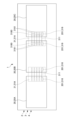
- FIG. 13 is an external view of a bridge according to a modified example of the present embodiment, as viewed from above. 13 is an external view of a connection layer of a modified example of the present embodiment as viewed from above.
- FIG. 13A to 13C are diagrams illustrating an alignment step in a bridge mounting step of mounting a bridge on a wiring layer. 11 is a cross-sectional view of an electronic device according to another embodiment of the present invention.
- the electronic device 1 according to one embodiment of the present invention will be described below with reference to the drawings.
- Fig. 1 is a cross-sectional view of the electronic device 1 according to one embodiment of the present invention.
- Fig. 2 is an exploded cross-sectional view of the electronic device 1 shown in Fig. 1. Note that reference numerals for detailed components are omitted in Fig. 1.
- the electronic device 1 includes an electronic component layer 2, a connection layer 3, and a wiring layer 4 (hereinafter referred to as "wiring layer 4") serving as an RDL (redistribution layer).
- the other electronic device 1 is mounted on a substrate 5.
- the electronic component layer 2 is formed by covering a first electronic component 20A, a second electronic component 20B, and a third electronic component 20C as multiple electronic components 20 with an insulating layer 21 described below.
- the electronic component layer 2 processes data using the electronic components 20.
- the electronic component layer 2 stores data and programs.
- the electronic component layer 2 executes programs.
- the electronic component layer 2 performs signal processing.
- the electronic component layer 2 performs communication.
- the electronic component layer 2 interfaces with a sensor device.
- the first electronic component 20A, the second electronic component 20B, and the third electronic component 20C may be referred to simply as "electronic components 20.”
- connection layer 3 is formed by covering one or more bridges 31 with an insulating layer 30, which will be described later.
- the connection layer 3 electrically connects the electronic component layer 2 and the wiring layer 4.
- the connection layer 3 is formed between the electronic component layer 2 and the wiring layer 4.
- the connection layer 3 may function as a so-called interposer.
- the multiple bridges 31 include a first bridge 31A and a second bridge 31B.
- first bridge 31A and the second bridge 31B may be simply referred to as "bridge 31.”
- the substrate 5 physically supports the electronic component layer 2, the connection layer 3, and the wiring layer 4.
- the substrate 5 functions as a wiring substrate.
- the substrate 5 is disposed on the opposite side of the wiring layer 4 from the electronic component layer 2 and the connection layer 3.
- the substrate 5 may be a glass epoxy substrate, or may be a substrate having an insulating layer and a wiring layer provided on a glass base material.
- the electronic component layer 2 has a plurality of electronic components 20 and an insulating layer 21.
- the plurality of electronic components 20 include a first electronic component 20A, a second electronic component 20B, and a third electronic component 20C.
- the electronic components 20 process data.
- the electronic components 20 store data and programs.
- the electronic components 20 execute programs.
- the electronic components 20 perform signal processing.
- the electronic components 20 perform communication.
- the electronic components 20 interface with sensor devices.
- Each electronic component 20 may perform a different function.
- the electronic components 20 may be, for example, logic ICs.
- the electronic components 20 may be, for example, SoCs (System on a chip).
- the electronic components 20 may include memory ICs.
- the electronic components may be, for example, DDR (Double Data Rate), LPDDR (Low-Power Double Data Rate), or HBM (High Bandwidth Memory).
- the electronic components 20 may be arranged so that multiple electronic components 20 are adjacent to one another. That is, a first electronic component 20A, a second electronic component 20B, and a third electronic component 20C may be arranged side by side on the electronic component layer 2. Note that the number of electronic components 20 is not limited to three. The number of electronic components may be two, three or more, or four or more.
- first electronic component 20A and the second electronic component 20B may be arranged side by side so as to be adjacent to each other.
- the second electronic component 20B and the third electronic component 20C may be arranged side by side so as to be adjacent to each other.
- the explanation regarding the first electronic component 20A and the second electronic component 20B which are adjacent to each other may also be applied to the other nth electronic component and (n+1)th electronic component which are adjacent to each other.
- n is a natural number.
- the electronic device 1 can process more information and perform more functions than if it had only one electronic component 20. For example, if there are three or more electronic components 20, the electronic device 1 can process more information and perform more functions.
- ICs integrated circuits
- a specific example of the multiple electronic components 20 is an IC chip (semiconductor chip).
- the IC chip has semiconductor elements arranged at high density.
- the IC chip has a chip substrate, transistors, chip wiring, and a chip insulating layer (not shown).
- the chip substrate is the substrate of the IC chip.
- Transistors function as electronic switches, controlling current in response to changes in voltage.
- An example of a transistor is a MOSFET (Metal-Oxide-Semiconductor Field-effect Transistor).
- Chip wiring is the electronic pathway for transmitting signals between transistors and other components. For example, chip wiring is formed into fine patterns using conductive metals (aluminum or copper). The chip insulation layer prevents shorting of the chip substrate, transistors, and chip wiring.
- the insulating layer 21 seals the periphery of the electronic component 20 including the transistor.
- the insulating layer 21 is, for example, an organic insulating layer such as an epoxy resin.
- the organic insulating layer may contain inorganic particles such as silica or alumina. The inclusion of inorganic particles makes it possible to control the linear expansion coefficient and elastic modulus.
- the insulating layer 21 may be a molded resin.
- the insulating layer 21 may be formed by transfer molding, in which a pellet-shaped material is heated and softened in a plunger, and then the resin is pressed into a mold and cooled and solidified to form the resin.
- the insulating layer 21 may be formed by laminating a build-up resin film and heat-curing it.
- the electronic component 20 has a first opposing portion 200 and an electronic component side electrode 201.
- a bump electrode 202 and a bump electrode 203 are formed on the electronic component side electrode 201.
- the first facing portion 200 faces the bridge 31. Specifically, the first facing portion 200 faces the bridge 31 via the insulating layer 21 of the electronic component layer 2.
- the first facing portion 200 may be a surface facing the bridge 31. Specifically, the first facing portion 200 may be a surface facing the bridge 31 via the insulating layer 21 of the electronic component layer 2.
- the first facing portion 200 may be the bottom surface of the electronic component 20 when the electronic device 1 shown in FIG. 1 is placed on a horizontal surface.
- the bump electrode 203 connected to the bridge electrode 3160 (described later) of the bridge side first electrode 316 (described later) is a signal line terminal
- the bump electrode 203 connected to the via electrode 3161 (described later) of the bridge side first electrode 316 (described later) is either a power supply terminal or a ground terminal.
- the bump electrodes 202 and 203 are formed on the electronic component side electrode 201.
- the bump electrodes 202 and 203 are formed from solder.
- the bump electrodes 202 and 203 may also be formed from copper, silver, gold, tin, or alloys thereof.
- the other bump electrodes described in this embodiment may also be formed from similar materials.
- connection layer 3 has an insulating layer 30, a bridge 31, and a pillar 32 as a connection layer through-electrode.
- the insulating layer 30 seals the periphery of the bridge 31.
- the insulating layer 30 is an organic insulating layer such as an epoxy resin.
- the organic insulating layer may contain inorganic particles such as silica or alumina. The inclusion of inorganic particles makes it possible to control the linear expansion coefficient and elastic modulus.
- the insulating layer 30 may be a molded resin.
- the insulating layer 30 may be formed by transfer molding, in which a pellet-shaped material is heated and softened in a plunger, and then the resin is pressed into a mold and cooled and solidified to form.
- the insulating layer 30 may be formed by laminating a build-up resin film and heat-hardening it.
- the bridge 31 is electrically connected to the electronic component 20. There may be two or more bridges 31. In this embodiment, the multiple bridges 31 include a first bridge 31A and a second bridge 31B. There may be three or more bridges.
- the electronic device 1 can process more information than if there was only one bridge 31.
- the bridge 31 electrically connects adjacent electronic components 20 to each other. That is, the first bridge 31A (nth bridge) electrically connects adjacent first electronic component 20A (nth electronic component) and second electronic component 20B ((n+1)th electronic component). Furthermore, the second bridge 31B ((n+1)th bridge) may electrically connect adjacent second electronic component 20B ((n+1)th electronic component) and third electronic component 20C ((n+2)th electronic component).
- the pillars 32 penetrate the connection layer 3 from the facing portion 33 facing the electronic component layer 2 to the facing portion 34 facing the wiring layer 4, electrically connecting the electronic components 20 to the wiring of the wiring layer 4.
- the pillars 32 are formed in the insulating layer 30.
- the pillars 32 directly electrically connect the electronic component layer 2 and the wiring layer 4.
- the pillars 32 are formed by penetrating the insulating layer 30 from the surface facing the electronic component layer 2 (facing portion 33) to the surface facing the wiring layer 4 (facing portion 34).
- the pillars 32 are formed in a cylindrical shape, and a cavity is formed.
- a conductor is formed on the inner circumferential surface of the cavity.
- the cavity may be filled with a conductor.
- a conductor is copper formed by a plating method.
- the pillar 32 has an exposed portion as a surface that is exposed at the opposing portion 34 on the wiring layer 4 side.
- the exposed portion on the wiring layer 4 side of the pillar 32 is electrically connected to the third layer line wiring 46 formed in the fourth opposing portion 40 of the wiring layer 4 described later.
- the pillar 32 has an exposed portion as a surface that is exposed to the opposing portion 33 on the electronic component layer 2 side.
- the exposed portion of the pillar 32 on the electronic component layer 2 side may be covered with a pillar electrode 320.
- the pillar electrode 320 is, for example, a conductive thin film.
- the pillar electrode 320 is made of copper. Note that the exposed portion of the pillar 32 on the electronic component layer 2 side may be the pillar electrode 320 without providing a conductive thin film.
- the pillar electrode 320 of the connection layer 3 is electrically connected to the bump electrode 202 of the electronic component layer 2.
- the pillar 32 is used, for example, as a power line or a ground line of the electronic component 20.
- the bridge 31 has a base material 310 selected from silicon, ceramics, and glass, a bridge wiring 311 and a bridge insulating layer 312 that constitute a bridge wiring section, a second opposing section 313, a third opposing section 314, and a bridge through via 315 as a bridge through electrode.
- the bridge 31 further has a first bridge side electrode 316 and a second bridge side electrode 317.
- the bridge 31 is formed of a base material 310 selected from silicon, ceramics, and glass.
- a base material 310 selected from silicon, ceramics, and glass.
- the base material 310 is made of glass, it is preferable to use non-alkali glass or quartz glass that does not contain alkaline components from the viewpoint of electrical reliability. It is also preferable to select a base material 310 having an appropriate linear expansion coefficient and elastic modulus from the viewpoint of reliability in relation to the physical properties of the electronic component layer 2, the connection layer 3, the wiring layer 4, and the substrate 5.
- the relative dielectric constant of silicon is, for example, 12.
- the relative dielectric constant of alkali-free glass is, for example, 5.8.
- the relative dielectric constant of quartz glass is, for example, 3.9. Dielectric loss is proportional to the relative dielectric constant. Therefore, the higher the relative dielectric constant, the greater the dielectric loss. Therefore, the bridge 31 that electrically connects multiple electronic components 20 can reduce dielectric loss when the substrate 310 is made of glass, compared to when it is made of silicon.
- Dielectric loss can have effects on the transmission of information between multiple electronic components 20, such as signal attenuation, limited bandwidth, increased delay, and signal distortion.
- Dielectric loss absorbs and attenuates the energy of a signal. As a result, the signal weakens as it travels along the wire, and signal quality decreases. Signal attenuation is a factor that limits the distance that information can be transmitted.
- Wiring with high dielectric loss can slow down signal transmission speeds because it takes longer for the signal to replenish the energy absorbed within the wiring. Large signal delays reduce the reliability of communication.
- Dielectric losses can cause signals to become distorted during transmission. Large dielectric losses affect the amplitude, phase, and waveform of the signal, reducing signal accuracy.
- the bridge wiring 311 electrically connects the multiple electronic devices 1 to each other.
- the bridge wiring 311 is, for example, a copper wiring.
- power and information can be exchanged directly between multiple electronic components 20 arranged on the electronic component layer 2 via the bridge wiring 311.
- the bridge insulating layer 312 insulates the bridge wiring 311.
- the bridge insulating layer 312 seals the bridge wiring 311.
- the bridge insulating layer 312 is formed on the electronic component layer 2 side of the glass substrate 310, i.e., near the second opposing portion 313.
- the bridge wiring section consisting of the bridge insulating layer 312 and the bridge wiring 311 may also be formed on the wiring layer 4 side of the glass substrate 310, i.e., near the third opposing portion 314.
- a via is formed in the bridge 31 to electrically connect the bridge-side first electrode 316 formed on the second opposing portion 313 of the bridge 31 to the bridge wiring 311 formed near the third opposing portion 314. This also improves the density of the electronic components 20 and the wiring.
- the bridge insulating layer 312 may be an inorganic insulating layer.
- the bridge insulating layer 312 may be silicon dioxide (SiO 2 ).
- the inorganic insulating layer such as silicon dioxide is formed by, for example, chemical vapor deposition (CVD).
- the second facing portion 313 of the bridge 31 faces the first facing portion 200 of each of the multiple electronic components 20. That is, the second facing portion 313 faces the first facing portion 200 of each of the first electronic component 20A, the second electronic component 20B, and the third electronic component 20C.
- the second facing portion 313 may be the upper surface of the bridge 31 when the electronic device 1 shown in FIG. 1 is placed on a horizontal surface.
- the current and information output from the second electronic component 20B is transmitted from the bump electrode 203 of the electronic component side electrode 201 to the bridge wiring 311 via the bridge electrode 3160 of the bridge side first electrode 316 formed on the second electronic component 20B side of the bridge 31.
- the first electronic component 20A receives the current and information transmitted to the bridge wiring 311 from the bridge electrode 3160 of the bridge side first electrode 316 formed on the first electronic component 20A side of the bridge 31 via the bump electrode 203 of the electronic component side electrode 201 of the first electronic component 20A.
- the bridge through via 315 is preferably a straight via electrode that penetrates from the second opposing portion 313 to the third opposing portion 314. That is, the bridge through via 315 is preferably a straight via electrode that penetrates the glass substrate 310 and the bridge insulating layer 312 in a straight line. This allows the wiring length to be shortened when electrically connecting the electronic component 20 and the wiring layer 4 via the bridge 31. This configuration is particularly effective when an HBM is used as the electronic component 20. In the HBM, the contacts of the signal lines are densely arranged, and the contacts of the power line and the ground line are also arranged near that portion.
- the power line of the electronic component 20 and the power line of the wiring layer 4 are connected via the bridge through via 315, so the connection distance between them is shortened.
- the ground line of the electronic component 20 and the ground line of the wiring layer 4 are connected via the bridge through via 315, so the connection distance between them is shortened.
- the bridge wiring 311 can be used as a signal line to electrically connect multiple electronic components 20 to each other with a short wiring length
- the bridge through via 315 can be used as a power line or ground line to electrically connect the electronic components 20 to the wiring layer 4 with a short wiring length.
- the bridge-side first electrode 316 includes a bridge electrode 3160 and a via electrode 3161.
- the bridge electrode 3160 is, for example, formed of a conductive thin film that extends from the bridge wiring 311 sealed in the bridge insulating layer 312 toward the electronic component 20 and electrically covers the exposed surface at the second opposing portion 313.
- the bridge electrode 3160 is formed of copper. Note that the exposed portion of the bridge wiring 311 on the second opposing portion 313 side may be used as the bridge electrode 3160 without providing a conductive thin film.
- the via electrode 3161 is formed, for example, from a conductive thin film that extends from the bridge through via 315 toward the electronic component 20 and covers the exposed portion as the surface exposed to the third opposing portion 314.
- the via electrode 3161 is formed from copper. Note that the exposed portion on the second opposing portion 313 side of the bridge wiring 311 may be used as the via electrode 3161 without providing a conductive thin film.
- a bridge-side second electrode 317 is formed on the third opposing portion 314. That is, the bridge-side second electrode 317 is formed on the third opposing portion 314 of the bridge 31. The bridge-side second electrode 317 is electrically connected to the third layer line wiring 46 of the wiring layer 4.
- the second bridge-side electrode 317 includes a via electrode 3170 and a bump electrode 3171.
- the bump electrode 3171 may have a structure in which a solder material is formed at the tip of a copper pillar, and preferably the solder contains tin and bismuth.
- the via electrode 3170 is formed, for example, from a conductive thin film that extends from the bridge through via 315 toward the wiring layer 4 and covers the exposed portion as the surface exposed to the third opposing portion 314.
- the via electrode 3170 is formed from copper. Note that the exposed portion of the bridge wiring 311 on the third opposing portion 314 side may be used as the via electrode 3170 without providing a conductive thin film.
- a bump electrode 3171 is formed on the via electrode 3170.
- the bump electrode 3171 is connected to either the power line or the ground line of the wiring layer 4.
- the fourth opposing portion 40 faces the third opposing portion 314 of the bridge 31. Specifically, the fourth opposing portion 40 faces the bridge 31 via the insulating layer 30 of the connection layer 3.
- the fourth opposing portion 40 may be a surface facing the bridge 31.
- the fourth opposing portion 40 may be a surface facing the bridge 31 via the insulating layer 30 of the connection layer 3.
- the fourth opposing portion 40 may be the upper surface of the wiring layer 4 when the electronic device 1 shown in FIG. 1 is placed on a horizontal surface.
- the fourth opposing portion 40 of the wiring layer 4 and the third opposing portion 314 of the bridge 31 of the connection layer 3 are electrically connected.
- the third-layer line wiring 46 of the fourth opposing portion 40 of the wiring layer 4 is electrically connected to the via electrode 3170 formed on the bridge 31 of the connection layer 3.
- the via electrode 3170 of the bridge-side second electrode 317 formed on the first electronic component 20A side is electrically connected to the third-layer line wiring 46 of the wiring layer 4.
- the via electrode 3170 of the bridge-side second electrode 317 formed on the second electronic component 20B side is electrically connected to the third-layer line wiring 46 of the wiring layer 4.
- the bridge 31 is metal-bonded to the wiring layer 4 by flip-chip mounting. This allows the bridge 31 to be mounted with extremely high positioning accuracy.
- the fifth opposing portion 41 is formed on the wiring layer 4 on the opposite side to the fourth opposing portion 40 of the wiring layer 4.
- the fifth opposing portion 41 faces the substrate 5.
- the fifth opposing portion 41 faces the substrate 5 via a bump electrode 49 formed on the fifth opposing portion 41.
- the fifth opposing portion 41 may be the underside of the wiring layer 4 when the electronic device 1 shown in FIG. 1 is placed on a horizontal surface.
- the first layer line wiring 42 is formed in the fifth opposing portion 41 of the wiring layer 4.
- the first layer line wiring 42 may be formed from copper wiring.
- the first insulating layer 43 insulates the first layer line wiring 42, the first layer via wiring 47, and the second layer line wiring 44.
- the first insulating layer 43 is formed on the top of the first layer line wiring 42 when the electronic device 1 shown in FIG. 1 is placed on a horizontal surface.
- the first insulating layer 43 can be formed of a resin such as polyimide, polybenzoxazole, or benzocyclobutene, for example. If these resins have a photosensitive function, vias (openings) can be formed by photolithography and filled with a conductive material such as metal to electrically connect the wiring layers formed above and below the resin material. If the resin material is not photosensitive, the vias can be opened by laser light irradiation or dry etching.
- the second layer line wiring 44 is laminated on the first insulating layer 43 on the side opposite the first layer line wiring 42.
- the second layer line wiring 44 is formed to improve the density of the electronic components 20 and wiring when multiple electronic components 20 are mounted in the electronic device 1 according to this embodiment.
- the second layer line wiring 44 is laminated on top of the first insulating layer 43 when the electronic device 1 shown in FIG. 1 is placed on a horizontal surface.
- the second layer line wiring 44 can be formed from the same composition as the first layer line wiring 42.
- the second insulating layer 45 insulates the second layer line wiring 44, the second layer via wiring 48, and the third layer line wiring 46.
- the second insulating layer 45 is laminated on top of the second layer line wiring 44 when the electronic device 1 shown in FIG. 1 is placed on a horizontal surface.
- the second insulating layer 45 can be formed with the same composition as the first insulating layer 43.
- the third layer line wiring 46 is formed in the fourth opposing portion 40 of the wiring layer 4. When the connection layer 3 and the wiring layer 4 are joined, the third layer line wiring 46 is electrically connected to the exposed portion of the pillar 32 formed in the connection layer 3 on the wiring layer 4 side. When the connection layer 3 and the wiring layer 4 are joined, the third layer line wiring 46 is electrically connected to the bridge side second electrode 317 of the bridge 31.
- the third layer line wiring 46 is laminated on top of the second insulating layer 45 when the electronic device 1 shown in FIG. 1 is placed on a horizontal surface.
- the third layer line wiring 46 can be formed from the same composition as the first layer line wiring 42 and the second layer line wiring 44.
- the first layer via wiring 47 electrically connects the first layer line wiring 42 and the second layer line wiring 44.
- the first layer via wiring 47 is formed to extend vertically from the first layer line wiring 42 to the second layer line wiring 44.
- the second layer via wiring 48 electrically connects the second layer line wiring 44 and the third layer line wiring 46.
- the second layer via wiring 48 is formed to extend vertically from the second layer line wiring 44 to the third layer line wiring 46.
- the bump electrode 49 electrically connects the wiring layer 4 and the substrate 5. When the wiring layer 4 and the substrate 5 are joined, the bump electrode 49 electrically connects the first layer line wiring 42 of the wiring layer 4 and wiring (not shown) of the substrate 5. The bump electrode 49 is formed on the fifth opposing portion 41.
- Fig. 3 is an external view of the electronic device 1 according to the present embodiment as viewed from above.
- FIG. 3 shows the first electronic component 20A, the second electronic component 20B, the third electronic component 20C, the first bridge 31A, and the second bridge 31B that are included in the electronic device 1 according to this embodiment.
- the bridge 31 is positioned so as to overlap each of the multiple electronic components 20.
- the electronic components 20 can be densely arranged on the electronic component layer 2. Therefore, in an electronic device 1 of specified dimensions, the amount of information that the electronic components 20 can process can be increased.
- a portion of the first electronic component 20A overlaps with a portion of the first bridge 31A.
- a portion of the second electronic component 20B overlaps with a portion of the first bridge 31A.
- a portion of the second electronic component 20B overlaps with a portion of the second bridge 31B.
- a portion of the third electronic component 20C overlaps with a portion of the second bridge 31B.
- the electronic component side electrode 201 of the first electronic component 20A overlaps with the bridge-side first electrode 316 of the first bridge 31A.
- the electronic component side electrode 201 of the second electronic component 20B overlaps with the bridge-side first electrode 316 of the first bridge 31A.
- the electronic component side electrode 201 of the second electronic component 20B overlaps with the bridge-side first electrode 316 of the second bridge.
- the electronic component side electrode 201 of the third electronic component 20C overlaps with the bridge-side first electrode 316 of the second bridge 31B. The same applies below.
- the bump electrode 203 of the electronic component side electrode 201 of the first electronic component 20A is electrically connected to the bridge electrode 3160 and via electrode 3161 of the bridge side first electrode 316 of the first bridge 31A.
- the bump electrode 203 of the electronic component side electrode 201 of the second electronic component 20B is electrically connected to the bridge electrode 3160 and via electrode 3161 of the bridge side first electrode 316 of the first bridge 31A.
- connection between the electrodes of the electronic component 20 and the connection layer 3 can be made using solder.
- the solder preferably contains tin as the main component and silver.
- the solder connection between the bridge and the wiring layer 4 is also heated to a certain extent in the process of connecting the electronic component to the connection layer 3. If the solder connecting the bridge and the wiring layer 4 melts at this time, the bridge may become misaligned.
- the melting point of this part can be made much higher than the melting point of the solder containing tin and silver as the main component. This is preferable because the solder connecting the bridge and the wiring layer 4 does not melt when the electronic component is soldered to the connection layer 3, and there is no adverse effect on the mounting accuracy of the bridge.
- the bridge 31 may be smaller than any of the multiple electronic components 20 connected to it.
- the first bridge 31A is smaller than the first electronic component 20A and smaller than the second electronic component 20B.
- the area of the first bridge 31A is smaller than the area of the first electronic component 20A and the area of the second electronic component 20B.
- the area of the first bridge 31A when viewed in a plan view is smaller than both the area of the first electronic component 20A and the area of the second electronic component 20B when viewed in a plan view.
- the proportion of the bridge 31 using the glass substrate 310 in the wiring layer 4 can be reduced, thereby preventing an increase in costs.
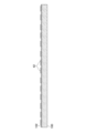
- FIG. 4A is a diagram showing the glass substrate preparation process for preparing glass substrate 310.
- glass substrate 310 is prepared.
- Glass substrate 310 is, for example, a glass wafer.
- FIGS. 4A to 4H show glass substrate 310 of the size of one bridge 31.
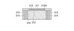
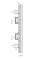
- FIG. 4B is a diagram showing a via filling process in which a via is filled in the formed through hole to form a part of the bridge through via 315 after the through hole forming process in which a through hole is formed in the glass substrate 310.
- a through hole is formed so as to penetrate from the first main surface 310A to the second main surface 310B (the third opposing portion 314 of the bridge 31) of the glass substrate 310.
- the through hole is formed, for example, by laser processing. It is also preferable to smooth the surface of the through hole by etching with hydrofluoric acid after the laser processing.
- the through hole is formed by forming a seed layer by sputtering film formation or electroless plating, and then forming a metal such as copper on it by electrolytic plating to perform a conductive process with low resistance.
- a metal layer may be formed only on the inner wall surface of the through hole, or the entire hole may be filled with metal.
- a via electrode is formed as at least a part of the bridge through via 315.
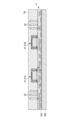
- FIG. 4C is a diagram showing an insulating film forming process for forming a bridge insulating layer 312 on the first main surface 310A of the glass substrate 310.
- the bridge insulating layer 312 is formed on the first main surface 310A of the glass substrate 310.
- the bridge insulating layer 312 is formed by depositing an organic insulating layer by, for example, spin coating. Polyimide, polybenzoxazole, benzocyclobutene, etc. can be used as the organic insulating film layer material. Alternatively, it is formed by depositing an inorganic insulating layer such as SiO 2 by CVD or the like.
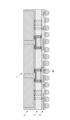
- FIG. 4D is a diagram showing a bridge wiring formation process for forming bridge wiring 311 on bridge insulating layer 312. As shown in FIG. 4D, on the first main surface 310A side of glass substrate 310, bridge wiring 311 is further formed on bridge insulating layer 312. Bridge wiring 311 is formed by additive method, for example. In additive method, resist is formed on bridge insulating layer 312, and bridge wiring 311 is formed by electroless plating (full additive method).
- a method of forming a seed layer made of titanium or copper by sputtering, forming a wiring pattern with resist, forming metal wiring such as copper by electrolytic plating, and then peeling off the resist, and etching away the seed layer between wiring to form wiring (semi-additive method) or damascene process can also be used.
- Copper wiring for example, is used as bridge wiring 311.
- FIG. 4E is a diagram showing an insulating film formation process for forming a bridge insulating layer 312 on the bridge wiring 311.
- a bridge insulating layer 312 is further formed on the bridge wiring 311 laminated on the bridge insulating layer 312, and the bridge wiring 311 is sealed with the bridge insulating layer 312.
- the bridge wiring section may be formed with a multi-layer wiring structure having multiple layers of bridge wiring 311 by repeating the process of FIG. 4D and the process of FIG. 4E.
- the bridge wiring section has multiple layers of bridge insulating layers 312 and multiple layers of bridge wiring 311, and the bridge insulating layers 312 and bridge wiring 311 are laminated alternately. This allows signals to be transmitted between multiple electronic components 20 using a large number of wirings.
- the wiring width becomes narrower and the number of wiring layers increases.
- the width of the bridge wiring and the spacing between the wiring are both 2 ⁇ m, in the case of 1024 bits, the number of bridge wiring layers may be six or more.
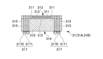
- FIG. 4F is a diagram showing a via filling process in which the openings formed in the bridge insulating layer 312 are filled with vias to form bridge through vias 315 after the opening forming process in which openings are formed in the bridge insulating layer 312.
- a via opening
- the conductive material is connected to a via electrode (not shown) of the glass substrate 310 to form the bridge through via 315.
- the via opening can also be formed by laser light irradiation or dry etching.
- FIG. 4G is a diagram showing the bridge wiring formation process.
- bridge wiring 311 is additionally formed so that bridge wiring 311 is exposed from second opposing portion 313.
- This additional wiring is formed by, for example, a damascene method or a semi-additive method.
- bridge wiring 311 is formed that is bent at both horizontal ends and has ends exposed at second opposing portion 313.
- FIG. 4H is a diagram showing the bump electrode formation process.
- a bridge-side second electrode 317 is formed on the third opposing portion 314 side of the bridge through via 315. That is, a via electrode 3170 is formed as a seed layer on the exposed portion on the third opposing portion 314 side of the bridge through via 315, and a bump electrode 3171 is further formed on the via electrode 3170. Note that the formation of the seed layer may be omitted.
- the bridge 31 is then cut to chip size by dicing, and the bridge 31 with the bump electrode formed is completed.
- FIGS 5A to 5O are diagrams showing the stacking process for the electronic device 1 according to an embodiment.
- FIG. 5A is a diagram showing a release layer forming process in which a release layer 102 is formed on the panel carrier 100 prepared in the panel carrier preparation process.
- a release layer 102 is formed on the panel carrier 100, which serves as a base.
- the material of the panel carrier can be preferably glass, ceramics such as alumina, silicon, etc.
- Glass carriers have a wide variety of linear expansion coefficients, and by using one with an appropriate linear expansion coefficient, the range of warping during the process can be kept within a certain range, which is preferable.
- Ceramic carriers have a large elastic modulus, which makes it easy to suppress warping after the formation of the wiring layer and the molding material, which is preferable.
- Silicon carriers have a high elastic modulus, which makes it effective in suppressing warping during the process, and it is easy to increase the flatness and smoothness of the surface, making it easy to form fine wiring, which is preferable.
- FIG. 5B is a diagram showing the wiring formation process for forming the first layer line wiring 42 on the release layer 102. As shown in FIG. 5B, a copper layer is formed on the release layer 102 to form the first layer line wiring 42.
- the patterned first layer line wiring 42 is formed, for example, by a damascene method or a semi-additive method.
- FIG. 5C is a diagram showing the wiring layer formation process for forming wiring layer 4 on release layer 102. As shown in FIG. 5C, wiring layer 4 is laminated on release layer 102.
- the wiring layer 4 is formed by stacking a first insulating layer 43, a second layer line wiring 44, a second insulating layer 45, and a third layer line wiring 46 in this order on the first layer line wiring 42.
- the first layer via wiring 47 may be formed after the first insulating layer 43 is formed.
- the second layer via wiring 48 may be formed after the second insulating layer 45 is formed.
- FIG. 5E is a diagram showing a resist film formation process, which is part of the pillar formation process. As shown in FIG. 5E, a thick resist film 104 is formed so as to cover the bridges 31 (first bridge 31A, second bridge 31B).
- FIG. 5F is a diagram showing a pillar formation process in which a via is filled in a hole formed in the resist film 104 to form a pillar 32 after the hole formation process in which a hole is formed in the resist film 104.
- a hole is formed by etching a predetermined portion of the resist film 104 (the contact portion in the third layer line wiring 46), and then the formed hole is filled with a via by electrolytic plating to form the pillar 32.
- via filling a seed layer is first formed on the inner surface of the hole by sputtering.
- a titanium film is used as the seed layer.
- the via is filled by electrolytic plating to form the pillar 32.
- the metal pillar as the pillar 32 is formed from, for example, copper.
- the following steps may be carried out in that order on the wiring layer 4 before mounting the bridge: applying resist, forming holes in the resist by lithography or the like, forming a seed layer by sputtering, forming pillars by electrolytic plating, and removing the resist, and then forming the pillars, after which the bridge, etc. may be mounted.
- FIG. 5G is a diagram showing the resist film removal process for removing the resist film 104. As shown in FIG. 5G, the resist film 104 is removed to expose the bridges 31 (first bridge 31A, second bridge 31B) and pillars 32.
- FIG. 5H is a diagram showing the molding process in which the bridge 31 and pillar 32 are covered with the insulating layer 30.
- the bridge 31 first bridge 31A, second bridge 31B
- pillar 32 are molded with the insulating layer 30.
- the space between the bridge 31 and the wiring layer 4 may be sealed with a capillary flow underfill material, and molding may then be performed.
- FIG. 5I is a diagram showing the grinding process for grinding the surface of the insulating layer 30.
- the surface of the insulating layer 30 is ground with a grinder or the like to expose the second opposing portion 313 of the bridge 31.
- the pillar 32 is also ground to form an exposed portion of the pillar 32 on the opposing portion 33 side of the connection layer 3 on the electronic component layer 2 side.
- FIG. 5J is a diagram showing the electrode formation process for forming electrodes made of thin film metal.
- a bridge electrode 3160 made of thin film metal is formed on the surface of the bridge wiring 311 exposed at the second opposing portion 313 of the bridge 31 (first bridge 31A, second bridge 31B), and a via electrode 3161 made of thin film metal is formed on the surface of the bridge through via 315.
- a pillar electrode 320 made of thin film metal is formed on the surface of the pillar 32.
- this process is not necessarily required, and the exposed surfaces of the bridge wiring 311, the bridge through via 315, and the pillar 32 may be used as electrodes as they are. In this way, the connection layer 3 is formed.
- FIG. 5K is a diagram showing the electronic component mounting process for mounting electronic components 20 on the connection layer 3.
- electronic components 20 (first electronic component 20A, second electronic component 20B, third electronic component 20C) are mounted on the connection layer 3 so as to overlap a part of bridge 31 (first bridge 31A, second bridge 31B).
- bump electrodes 203 and 202 of electronic components 20 (first electronic component 20A, second electronic component 20B, third electronic component 20C) are bonded to bridge 31 (first bridge 31A, second bridge 31B) and pillar 32.
- electronic components 20 are metallically bonded to connection layer 3 by flip-chip mounting. This allows electronic components 20 to be mounted with extremely high positioning accuracy.
- FIG. 5L is a diagram showing a molding process in which electronic components 20 are covered with insulating layer 21. As shown in FIG. 5L, electronic components 20 (first electronic component 20A, second electronic component 20B, third electronic component 20C) are molded with insulating layer 21.
- Figure 5M shows the grinding process for grinding the surface of insulating layer 21.
- insulating layer 21 is ground with a grinder or the like to expose the surfaces of electronic components 20 (first electronic component 20A, second electronic component 20B, third electronic component 20C). This process is not necessarily required, but is useful when forming a heat dissipation structure directly on electronic component 20 for heat dissipation.
- FIG. 5N is a diagram showing the panel carrier removal process for removing the panel carrier 100. As shown in FIG. 5N, the panel carrier 100 and the release layer 102 are removed.
- Figure 5O is a diagram showing the bump electrode formation process for forming bump electrodes 49 on the wiring layer 4. As shown in Figure 5O, bump electrodes 49 are formed on the first-layer line wiring 42 of the wiring layer 4. This completes the electronic device 1. The electronic device 1 is then mounted on the substrate 5 using the bump electrodes 49.
- Figs. 6A to 6C show modified examples of this embodiment.
- Fig. 6A is an external view of the bridge 31 of the modified example as viewed from above (planar view).
- Fig. 6B is an external view of the wiring layer 4 as viewed from above (planar view).
- Fig. 6C is a diagram showing an alignment process in the bridge mounting process in which the bridge 31 is mounted on the wiring layer 4. Note that the third layer line wiring 46 is omitted from Figs. 6B and 6C.
- the bridge 31 has a first alignment mark 50A as an alignment mark.
- the first alignment mark 50A is disposed near the second opposing portion 313 (see FIG. 4H).
- the first alignment mark 50A is disposed, for example, in the bridge insulating layer 312.
- the first alignment mark 50A may be disposed in the same layer in which the bridge wiring 311 is disposed.
- the first alignment mark 50A may be made of the same material as the bridge wiring 311. This makes the process of forming the alignment mark easier.
- the first alignment mark 50A may be disposed in a layer different from the layer in which the bridge wiring 311 is disposed.
- the first alignment mark 50A may be made of a material different from the bridge wiring 311.
- the first alignment mark 50A is arranged in the same layer as the bridge wiring 311, but spaced apart from the bridge wiring 311. In this way, the first alignment mark 50A is provided separately from the bridge wiring 311, making it possible to perform more accurate alignment. However, a part of the bridge wiring 311 may also serve as the first alignment mark 50A.
- the first alignment mark 50A has a shape corresponding to the second alignment mark 50B arranged on the wiring layer 4 described below.
- the first alignment mark 50A is, for example, a cross-shaped mark. However, it is not limited to this.
- first alignment marks 50A are provided, and more preferably, three or more are provided. In this modified example, three first alignment marks 50A are provided.
- the first alignment mark 50A may be disposed on the surface of the second opposing portion 313 (see FIG. 4H).
- the first alignment mark 50A may be disposed on the bridge insulating layer 312.
- the first alignment mark 50A may also be disposed on the glass substrate 310 on the second opposing portion 313 side.
- the first alignment mark 50A may be disposed near the third opposing portion 314 (see FIG. 4H).
- the first alignment mark 50A disposed near the third opposing portion 314 can be recognized by a camera through the glass substrate 310.
- the first alignment mark 50A may be disposed on the surface of the third opposing portion 314.
- the first alignment mark 50A may also be disposed on the glass substrate 310 on the third opposing portion 314 side.
- the first alignment mark 50A may be disposed on the light-transmitting insulating layer.
- the distance to the second alignment mark 50B described later becomes closer, so that the alignment accuracy can be improved.
- the wiring layer 4 has a second alignment mark 50B.
- the second alignment mark 50B is provided on the surface of the wiring layer 4.
- the second alignment mark 50B may be made of the same material as the third layer line wiring 46. This makes the process of forming the alignment mark easier. However, the second alignment mark 50B may be made of a material different from that of the third layer line wiring 46.
- the second alignment mark 50B has a shape corresponding to the first alignment mark 50A.
- the second alignment mark 50B is, for example, a mark made up of four rectangles. However, this is not limited to this.
- second alignment marks 50B are provided, and more preferably, three or more are provided. In this modified example, three second alignment marks 50B are provided. The second alignment marks 50B are provided in a number corresponding to the number of first alignment marks 50A.
- FIG. 6C is a diagram for explaining the alignment process when flip-chip mounting bridge 31 on wiring layer 4.
- FIG. 6C is a top view of wiring layer 4 and bridge 31 arranged on wiring layer 4. Specifically, it is a plan view of FIG. 5D from the top to the bottom of the paper.
- the bridge 31 is made of a translucent material from the second opposing portion 313 to the third opposing portion 314.
- the glass substrate 310 of the bridge 31 is a translucent material.
- the bridge insulating layer 312 is made of a translucent material.
- the bridge insulating layer 312 is preferably a translucent resin material or a translucent inorganic material.
- the translucent resin material is not particularly limited as long as it is translucent, and epoxy, polyimide, polybenzoxazole, benzocyclobutene, etc. can be used. As long as translucency is ensured, particles may be dispersed in these resins.
- the material of the particles is not particularly limited, and silica, alumina, barium sulfate, talc, aluminum nitride, silicon nitride, silicon carbide, etc. can be used.
- the translucent inorganic material is not particularly limited, and for example, silicon oxide, silicon nitride, silicon carbonitride, aluminum oxide, etc. can be used.
- the surface of the wiring layer 4 can be seen through the bridge 31, except for the wiring parts such as the bridge wiring 311 provided on the bridge 31.
- the second alignment mark 50B arranged on the wiring layer 4 can be confirmed by the camera through the bridge 31. Furthermore, when the first alignment mark 50A is arranged near the third opposing portion 314, the first alignment mark 50A arranged near the third opposing portion 314 can also be confirmed by the camera through the glass substrate 310 of the bridge 31.
- the first alignment mark 50A of the bridge 31 is aligned with the second alignment mark 50B of the wiring layer 4, thereby accurately aligning the position and rotation direction of the bridge 31 on the wiring layer 4.
- flip-chip mounting is performed.
- flip-chip mounting by metal bonding is possible after accurate alignment, so the bridge 31 can be mounted with higher positional accuracy.
- first alignment marks 50A and second alignment marks 50B are provided in order to accurately align the position and rotation direction of the bridge 31 on the wiring layer 4. More preferably, there are three or more first alignment marks 50A and second alignment marks 50B. It is preferable that a plurality of first alignment marks 50A are arranged near the outer periphery of the bridge 31 in a planar view. When the shape of the bridge 31 is rectangular in a planar view, it is preferable that the alignment marks are provided at two or more, preferably three or more, of the four corners of the rectangular shape.
- the first alignment mark 50A is formed as an alignment mark on the glass bridge 31 formed from the glass substrate.
- the first alignment mark 50A may be formed on either the second opposing portion 313 side or the third opposing portion 314 side.
- the first alignment mark 50A is formed on the third opposing portion 314 side, it is preferable that it is formed so that it can be recognized through the glass substrate 310 from the second opposing portion 313 side.
- the first alignment mark 50A can be observed from the second opposing portion 313 side, when performing alignment when mounting the glass bridge 31 on the wiring layer 4, the first alignment mark 50A formed on the glass bridge 31 and the second alignment mark 50B formed on the wiring layer 4 can be recognized from the second opposing portion 313 side of the glass bridge 31 with a single camera, and further, it is possible to perform position recognition and position correction with the camera until the glass bridge 31 comes into contact with the wiring layer 4, thereby improving the mounting accuracy of the glass bridge 31.
- the first alignment mark 50A is formed on the second opposing portion 313 side, if the first alignment mark 50A and the second alignment mark 50B can be observed simultaneously from the second opposing portion 313 side, then when performing alignment when mounting the glass bridge 31 on the wiring layer 4, the first alignment mark 50A formed on the glass bridge 31 and the second alignment mark 50B formed on the wiring layer 4 can be recognized with a single camera from the second opposing portion 313 side of the glass bridge 31, and further, position recognition and position correction can be performed with the camera until the glass bridge 31 comes into contact with the wiring layer 4, improving the mounting accuracy of the glass bridge 31.
- FIG. 7 is a cross-sectional view of an electronic device according to another embodiment of the present invention. Note that the electronic device 1A has the same basic configuration as the electronic device 1, so only the differences will be described below.
- the electronic device 1A has a second wiring layer 6 between the electronic component layer 2 and the connection layer 3.
- the second wiring layer 6 has power wiring and ground wiring, similar to the wiring layer 4, which are connected to the power line and ground line of the wiring layer 4 via pillars 32, respectively.
- the second wiring layer 6 has signal wiring, which, like the bridge wiring 311, is responsible for transmitting signals between the electronic components 20A, 20B, and 20C.
- This embodiment also provides an electronic device 1 that allows the bridge 31 to be mounted on the wiring layer 4 with high positional accuracy.
- the electronic device 1 of this embodiment includes a bridge 31 that electrically connects multiple electronic components 20 together, and a wiring layer 4 having wiring, and the bridge 31 is metal-bonded to the wiring layer 4. This makes it possible to provide an electronic device 1 in which the bridge 31 can be mounted on the wiring layer 4 with high positional accuracy.
- the electronic device 1 of (1) includes a plurality of electronic components 20, each of which has a first facing portion 200 facing the bridge 31.
- the bridge 31 has a second facing portion 313 facing the first facing portion 200 of the plurality of electronic components 20 and a third facing portion 314 formed on the opposite side of the second facing portion 313.
- the bridge 31 has a bridge through electrode 315 (bridge through via 315) that penetrates from the second facing portion 313 to the third facing portion 314, and the bridge through electrode 315 (bridge through via 315) is metal-bonded to the wiring layer 4. This makes it possible to shorten the wiring length when electrically connecting the electronic component 20 to another layer via the bridge 31, and to mount the bridge 31 with high positional accuracy on the wiring layer 4.
- the power supply line of the electronic component 20 and the power supply line of the wiring layer 4 can be connected over a short distance.
- the ground line of the electronic component 20 and the ground line of the wiring layer 4 can be connected over a short distance.
- the bridge 31 further includes bridge wiring 311 that electrically connects the multiple electronic components 20 to each other. This allows the multiple electronic components 20 to directly exchange power and information with each other via the bridge wiring 311.
- the bridge 31 further includes a bridge insulating layer 312 that insulates the bridge wiring 311. This makes it possible to prevent short circuits between the multiple bridge wirings 311 and between the bridge wiring 311 and the bridge through via 315.
- the bridge insulating layer 312 is an organic insulating layer.
- An organic insulating layer formed from a resin material generally has a low relative dielectric constant. Therefore, by using an organic insulating layer as the bridge insulating layer 312, it is possible to further reduce dielectric loss. In addition, by using an organic insulating layer, it is possible to thicken the bridge insulating layer 312 in conjunction with the thickening of the bridge wiring 311, and even in this case, it is possible to reduce manufacturing costs.
- the electronic device 1 of (1) to (4) includes an electronic component layer 2 having a plurality of electronic components 20, a wiring layer 4 having wiring, and a connection layer 3 having a bridge 31 and electrically connecting the plurality of electronic components 20 to the wiring layer 4.
- the effects of the present disclosure can also be obtained with an electronic device 1 having such a configuration.
- the bridge through electrodes 315 (bridge through vias 315) electrically connect the multiple electronic components 20 to the wiring of the wiring layer 4. This makes it possible to shorten the wiring length when electrically connecting the electronic components 20 to other layers via the bridges 31.
- connection layer 3 has an insulating layer 30 that covers the periphery of the bridge 31, and the insulating layer 30 has a connection layer through electrode 32 (pillar 32) that penetrates from the facing portion (second facing portion 313) facing the electronic component layer 2 to the facing portion (third facing portion 314) facing the wiring layer 4, electrically connecting the electronic component 20 to the wiring of the wiring layer 4.
- pillar 32 connection layer through electrode 32
- the bridge 31 is arranged so as to overlap each of the multiple electronic components 20. This allows the electronic components 20 to be arranged densely in the electronic component layer 2. Therefore, in an electronic device 1 of specified dimensions, the amount of information that the electronic components 20 can process can be increased.
- the multiple electronic components 20 include at least the first electronic component 20A, the second electronic component 20B, and the third electronic component 20C
- the multiple bridges 31 include a first bridge 31A that electrically connects the first electronic component 20A and the second electronic component 20B to each other, and a second bridge 31B that electrically connects the second electronic component 20B and the third electronic component 20C to each other.
- the bridges were fixed to the wiring layer with an adhesive. In this case, the positioning accuracy of the bridges relative to the wiring layer was low. In this embodiment, flip-chip mounting by metal bonding is possible, so the bridges 31 can be mounted with high positional accuracy.
- the bridge 31 is formed from a glass substrate. This makes it possible to provide an electronic device 1 with reduced dielectric loss.
- the bridge 31 has a second facing portion 313 facing the first facing portion 200 of the multiple electronic components 20 and a third facing portion 314 formed on the opposite side of the second facing portion 313, at least a portion of the bridge 31 is made of a translucent material from the second facing portion 313 to the third facing portion 314, and the bridge 31 has a first alignment mark 50A. This makes it possible to mount the bridge 31 after performing accurate alignment, and therefore the bridge 31 can be mounted with higher positional accuracy.
- the bridge 31 is smaller than any of the electronic components 20. This allows the amount of material used to form the bridge 31 to be reduced, thereby reducing costs.
- a method for manufacturing an electronic device (1) including a bridge (31) that electrically connects a plurality of electronic components (20) and a wiring layer (4) having wiring comprising the steps of:
- the method includes a bridge manufacturing process for manufacturing the bridge 31, and a bridge mounting process for mounting the bridge 31 on the wiring layer 4,
- the bridge manufacturing process is as follows: Providing a substrate 310; a through-hole forming step of forming a through-hole in the base material 310; a bridge through electrode forming step of forming a bridge through electrode 315 (bridge through via 315) in the through hole; a bump electrode forming step of forming a bump electrode 203 corresponding to the bridge through electrode 315 (bridge through via 315);
- the bridge mounting process is as follows: The bridge 31 manufactured in the bridge manufacturing process is metal-bonded to the wiring layer 4 by flip-chip mounting. This makes it possible to provide the electronic device 1 in which the bridge 31 can be mounted on the wiring layer 4 with high positional accuracy
- the bridge 31 is formed of a light-transmitting glass substrate and has a first alignment mark 50A (alignment mark).
- the wiring layer 4 has a second alignment mark 50B corresponding to the first alignment mark 50A of the bridge 31,
- the bridge mounting process is a manufacturing method for electronic devices in which a single camera recognizes the first alignment mark 50A formed on the bridge 31 and the second alignment mark 50B formed on the wiring layer 4, and the bridge 31 and the wiring layer 4 are metal-bonded by flip-chip mounting. This makes it possible to mount the bridge 31 after performing accurate alignment, and therefore the bridge 31 can be mounted with higher positional accuracy.
Landscapes
- Engineering & Computer Science (AREA)
- Microelectronics & Electronic Packaging (AREA)
- Production Of Multi-Layered Print Wiring Board (AREA)
- Structure Of Printed Boards (AREA)
- Wire Bonding (AREA)
- Structures For Mounting Electric Components On Printed Circuit Boards (AREA)
Priority Applications (1)
| Application Number | Priority Date | Filing Date | Title |
|---|---|---|---|
| TW113145289A TW202545041A (zh) | 2023-11-30 | 2024-11-25 | 電子裝置 |
Applications Claiming Priority (2)
| Application Number | Priority Date | Filing Date | Title |
|---|---|---|---|
| JP2023203322A JP2025088548A (ja) | 2023-11-30 | 2023-11-30 | 電子装置 |
| JP2023-203322 | 2023-11-30 |
Publications (1)
| Publication Number | Publication Date |
|---|---|
| WO2025115520A1 true WO2025115520A1 (ja) | 2025-06-05 |
Family
ID=95897661
Family Applications (1)
| Application Number | Title | Priority Date | Filing Date |
|---|---|---|---|
| PCT/JP2024/039125 Pending WO2025115520A1 (ja) | 2023-11-30 | 2024-11-01 | 電子装置 |
Country Status (3)
| Country | Link |
|---|---|
| JP (1) | JP2025088548A (https=) |
| TW (1) | TW202545041A (https=) |
| WO (1) | WO2025115520A1 (https=) |
Citations (4)
| Publication number | Priority date | Publication date | Assignee | Title |
|---|---|---|---|---|
| JP2014022465A (ja) * | 2012-07-13 | 2014-02-03 | Shinko Electric Ind Co Ltd | 配線基板及びその製造方法 |
| JP2018523925A (ja) * | 2015-08-21 | 2018-08-23 | クアルコム,インコーポレイテッド | リソエッチング可能層内にブリッジを備える集積デバイスパッケージ |
| JP2021153173A (ja) * | 2020-03-24 | 2021-09-30 | インテル・コーポレーション | オープンキャビティブリッジ電力供給のアーキテクチャおよびプロセス |
| JP2021532578A (ja) * | 2018-07-24 | 2021-11-25 | インターナショナル・ビジネス・マシーンズ・コーポレーションInternational Business Machines Corporation | チップとパッケージ基板との間の電源接続を提供するチップ相互接続ブリッジを有するマルチチップ・パッケージ構造体 |
Family Cites Families (2)
| Publication number | Priority date | Publication date | Assignee | Title |
|---|---|---|---|---|
| TWI768294B (zh) * | 2019-12-31 | 2022-06-21 | 力成科技股份有限公司 | 封裝結構及其製造方法 |
| US20230207475A1 (en) * | 2021-12-23 | 2023-06-29 | Intel Corporation | Hybrid bonded stacked memory with tsv as chiplet for package structure |
-
2023
- 2023-11-30 JP JP2023203322A patent/JP2025088548A/ja active Pending
-
2024
- 2024-11-01 WO PCT/JP2024/039125 patent/WO2025115520A1/ja active Pending
- 2024-11-25 TW TW113145289A patent/TW202545041A/zh unknown
Patent Citations (4)
| Publication number | Priority date | Publication date | Assignee | Title |
|---|---|---|---|---|
| JP2014022465A (ja) * | 2012-07-13 | 2014-02-03 | Shinko Electric Ind Co Ltd | 配線基板及びその製造方法 |
| JP2018523925A (ja) * | 2015-08-21 | 2018-08-23 | クアルコム,インコーポレイテッド | リソエッチング可能層内にブリッジを備える集積デバイスパッケージ |
| JP2021532578A (ja) * | 2018-07-24 | 2021-11-25 | インターナショナル・ビジネス・マシーンズ・コーポレーションInternational Business Machines Corporation | チップとパッケージ基板との間の電源接続を提供するチップ相互接続ブリッジを有するマルチチップ・パッケージ構造体 |
| JP2021153173A (ja) * | 2020-03-24 | 2021-09-30 | インテル・コーポレーション | オープンキャビティブリッジ電力供給のアーキテクチャおよびプロセス |
Also Published As
| Publication number | Publication date |
|---|---|
| TW202545041A (zh) | 2025-11-16 |
| JP2025088548A (ja) | 2025-06-11 |
Similar Documents
| Publication | Publication Date | Title |
|---|---|---|
| US10672750B2 (en) | Semiconductor device | |
| US9620494B2 (en) | Hybrid substrates, semiconductor packages including the same and methods for fabricating semiconductor packages | |
| US7414309B2 (en) | Encapsulated electronic part packaging structure | |
| US10573615B2 (en) | Semiconductor package and method for fabricating base for semiconductor package | |
| JP5091221B2 (ja) | 半導体装置 | |
| CN101276809B (zh) | 半导体器件及其制造方法 | |
| TWI544599B (zh) | 封裝結構之製法 | |
| CN120319666B (zh) | 2.5d衬底封装方法和封装结构 | |
| CN116130456A (zh) | 一种芯片高密度互连封装结构及其制作方法 | |
| TW201737452A (zh) | 系統級封裝及用於製造系統級封裝的方法 | |
| CN118919517A (zh) | 一种实现局部高密度互连的半导体封装结构及其制造方法 | |
| JP5171726B2 (ja) | 半導体装置 | |
| US12148688B2 (en) | Semiconductor substrate and manufacturing method thereof | |
| WO2025115520A1 (ja) | 電子装置 | |
| WO2025115521A1 (ja) | 電子装置 | |
| CN118782583A (zh) | 一种集成无源器件的桥连结构及其制造方法 | |
| TW202447875A (zh) | 半導體封裝用基板、半導體封裝件以及半導體封裝用基板製造方法 | |
| US20240321755A1 (en) | Semiconductor package including glass core substrate and method of manufacturing the same | |
| JP2989271B2 (ja) | ベアチップ搭載ボード、ベアチップ搭載ボードの製造方法及びベアチップの電極形成方法 | |
| KR20250147857A (ko) | 유리 기판, 유리 기판을 포함하는 반도체 패키지 및 그 제조 방법 | |
| CN121237736A (zh) | 一种无源器件的封装结构及其制备方法 | |
| CN121729096A (zh) | 半导体封装结构及半导体封装结构的制备方法 | |
| CN116825855A (zh) | 半导体封装件 |
Legal Events
| Date | Code | Title | Description |
|---|---|---|---|
| 121 | Ep: the epo has been informed by wipo that ep was designated in this application |
Ref document number: 24897209 Country of ref document: EP Kind code of ref document: A1 |