WO2025100196A1 - 透明導電性フィルム - Google Patents
透明導電性フィルム Download PDFInfo
- Publication number
- WO2025100196A1 WO2025100196A1 PCT/JP2024/037171 JP2024037171W WO2025100196A1 WO 2025100196 A1 WO2025100196 A1 WO 2025100196A1 JP 2024037171 W JP2024037171 W JP 2024037171W WO 2025100196 A1 WO2025100196 A1 WO 2025100196A1
- Authority
- WO
- WIPO (PCT)
- Prior art keywords
- transparent conductive
- layer
- conductive film
- transmittance
- substrate
- Prior art date
- Legal status (The legal status is an assumption and is not a legal conclusion. Google has not performed a legal analysis and makes no representation as to the accuracy of the status listed.)
- Pending
Links
Images
Classifications
-
- B—PERFORMING OPERATIONS; TRANSPORTING
- B32—LAYERED PRODUCTS
- B32B—LAYERED PRODUCTS, i.e. PRODUCTS BUILT-UP OF STRATA OF FLAT OR NON-FLAT, e.g. CELLULAR OR HONEYCOMB, FORM
- B32B7/00—Layered products characterised by the relation between layers; Layered products characterised by the relative orientation of features between layers, or by the relative values of a measurable parameter between layers, i.e. products comprising layers having different physical, chemical or physicochemical properties; Layered products characterised by the interconnection of layers
- B32B7/02—Physical, chemical or physicochemical properties
- B32B7/023—Optical properties
-
- B—PERFORMING OPERATIONS; TRANSPORTING
- B32—LAYERED PRODUCTS
- B32B—LAYERED PRODUCTS, i.e. PRODUCTS BUILT-UP OF STRATA OF FLAT OR NON-FLAT, e.g. CELLULAR OR HONEYCOMB, FORM
- B32B7/00—Layered products characterised by the relation between layers; Layered products characterised by the relative orientation of features between layers, or by the relative values of a measurable parameter between layers, i.e. products comprising layers having different physical, chemical or physicochemical properties; Layered products characterised by the interconnection of layers
- B32B7/02—Physical, chemical or physicochemical properties
- B32B7/025—Electric or magnetic properties
-
- G—PHYSICS
- G02—OPTICS
- G02B—OPTICAL ELEMENTS, SYSTEMS OR APPARATUS
- G02B1/00—Optical elements characterised by the material of which they are made; Optical coatings for optical elements
- G02B1/10—Optical coatings produced by application to, or surface treatment of, optical elements
- G02B1/11—Anti-reflection coatings
- G02B1/111—Anti-reflection coatings using layers comprising organic materials
-
- G—PHYSICS
- G02—OPTICS
- G02B—OPTICAL ELEMENTS, SYSTEMS OR APPARATUS
- G02B1/00—Optical elements characterised by the material of which they are made; Optical coatings for optical elements
- G02B1/10—Optical coatings produced by application to, or surface treatment of, optical elements
- G02B1/14—Protective coatings, e.g. hard coatings
-
- H—ELECTRICITY
- H01—ELECTRIC ELEMENTS
- H01B—CABLES; CONDUCTORS; INSULATORS; SELECTION OF MATERIALS FOR THEIR CONDUCTIVE, INSULATING OR DIELECTRIC PROPERTIES
- H01B5/00—Non-insulated conductors or conductive bodies characterised by their form
- H01B5/14—Non-insulated conductors or conductive bodies characterised by their form comprising conductive layers or films on insulating-supports
Definitions
- the present invention relates to a transparent conductive film.
- transparent conductive films in which a metal oxide layer such as an indium tin composite oxide layer (ITO layer) is formed on a resin film have been widely used as transparent conductive films for use in electrodes for touch sensors, etc.
- ITO layer indium tin composite oxide layer
- the use of transparent conductive films as heating elements has also been considered, and they are sometimes used, for example, in covers for cameras and sensors used in automatic driving of automobiles for the purposes of melting snow and preventing fogging. In such uses, they are required to have excellent conductivity and to transmit the light used favorably.
- the transmittance of light in the near-infrared range may also be required.
- the present invention was made to solve the above problems, and its main objective is to provide a transparent conductive film that also has excellent near-infrared transmittance.
- a transparent conductive film according to an embodiment of the present invention is a transparent conductive film comprising, in this order, a conductive layer, a substrate, and a transmittance adjusting layer, wherein the transmittance adjusting layer has an arithmetic surface roughness Ra of 1.5 nm or more, and the maximum transmittance (T1max) of the transparent conductive film at a wavelength of 780 nm to 1600 nm and the maximum transmittance (T2max) of a laminate including the conductive layer and the substrate constituting the transparent conductive film at a wavelength of 780 nm to 1600 nm satisfy the following formula: ((T1max-T2max)/T2max) ⁇ 100 ⁇ 3%.
- the substrate may have a total light transmittance of 85% or more.
- the transmittance adjusting layer may have a maximum height roughness Rz of 12 nm or more.
- the transmittance adjusting layer may have a thickness of 120 nm or more.
- the transparent conductive film may further include a surface roughness adjustment layer between the substrate and the transmittance adjustment layer, and the surface roughness adjustment layer may contain particles having a particle diameter of 0.5 ⁇ m to 3.5 ⁇ m.
- a transparent conductive film that also has excellent translucency in the near-infrared region.
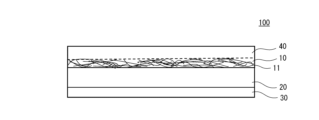
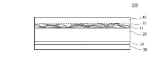
- 1 is a schematic cross-sectional view of a transparent conductive film according to one embodiment of the present invention. 1 is a schematic cross-sectional view of a transparent conductive film according to one embodiment of the present invention.
- FIG. 1 is a schematic cross-sectional view of a transparent conductive film according to one embodiment of the present invention.
- the transparent conductive film 100 includes a conductive layer 10, a substrate 20, and a transmittance adjusting layer 30 in this order.
- the transparent conductive film may further include any other appropriate layers.
- the conductive layer 10 includes a fiber-based conductive material 11, but the conductive layer may be, for example, a layer made of a metal film or a layer made of a metal oxide film.
- the transparent conductive film 100 includes a protective layer 40 disposed on the conductive layer 10 opposite the substrate 20.
- the protective layer 40 can be a layer that protects the fiber-based conductive material 11.
- the durability of the conductive layer 10 can be improved by providing the protective layer 40. More specifically, a conductive layer made of a fiber-based conductive material (e.g., metal nanowires) is characterized by low scratch resistance and moisture resistance, and by providing a protective layer, these problems can be eliminated and the durability of the conductive layer (and thus the durability of the transparent conductive film) can be improved.
- the conductive layer 10 may contain a component that constitutes the protective layer 40 (e.g., a resin that constitutes the protective layer).
- FIG. 2 is a schematic cross-sectional view of a transparent conductive film according to one embodiment of the present invention.
- the transparent conductive film 200 further includes a surface roughness adjustment layer 50 between the substrate 20 and the transmittance adjustment layer 30.
- the surface roughness adjustment layer 50 includes particles having a particle diameter (weight average particle diameter) of 0.5 ⁇ m to 3.5 ⁇ m.
- the unevenness caused by the particles affects the surface shape of the transmittance adjustment layer, and the surface roughness of the transmittance adjustment layer (the surface roughness of the surface opposite to the surface roughness adjustment layer) can be adjusted.
- the refractive index of the transmittance adjustment layer can be favorably maintained while the surface roughness of the transmittance adjustment layer can be adjusted.
- the maximum transmittance (T1max) of the transparent conductive film at a wavelength of 780 nm to 1600 nm and the maximum transmittance (T2max) of a laminate including a conductive layer and a substrate constituting the transparent conductive film at a wavelength of 780 nm to 1600 nm satisfy the following formula: ((T1max-T2max)/T2max) ⁇ 100 ⁇ 3%
- the "laminate consisting of a conductive layer and a substrate constituting a transparent conductive film” refers to a laminate consisting of a substrate and a conductive layer disposed on one surface of the substrate, and may be, for example, a transparent conductive film without a transmittance adjusting layer.
- the value expressed by ((T1max-T2max)/T2max) x 100 is also referred to as the increase rate of transmittance due to the transmittance adjusting layer.
- a transparent conductive film having low resistance and excellent light transmittance can be provided.
- a transparent conductive film suitable for use in transmitting laser light in the near-infrared region can be provided.
- the transparent conductive film can be suitably used, for example, in the field of autonomous driving of vehicles using LiDAR (Light Detection and Ranging), as a member that can efficiently transmit laser light (near-infrared region) required for sensing.
- the transparent conductive film is used in a transparent heater (for example, a transparent heater for a vehicle).
- the transparent heater can have any appropriate configuration.
- the transparent heater can be configured to generate heat by passing electricity through a transparent conductive film having a pair of electrodes arranged thereon.
- the transparent conductive film can be used as a heat source, and is advantageous in that it has excellent transmittance of near-infrared light and can generate sufficient heat even at a low voltage.
- ((T1max-T2max)/T2max) x 100" is preferably 3.5% or more, and more preferably 4% or more. Within this range, the above effects are prominent.
- the upper limit of "((T1max-T2max)/T2max) x 100" is, for example, 10%.
- the maximum transmittance (T1max) of the transparent conductive film at wavelengths of 780 nm to 1600 nm is preferably 85% or more, more preferably 90% or more, and even more preferably 94% or more.
- the maximum transmittance (T2max) of the laminate consisting of the conductive layer and the substrate that constitute the transparent conductive film at wavelengths of 780 nm to 1600 nm is, for example, 80% to 95%.
- the maximum transmittance (T3max) of the transparent conductive film at a wavelength of 380 nm to 780 nm and the maximum transmittance (T4max) of a laminate including a conductive layer and a substrate constituting the transparent conductive film at a wavelength of 380 nm to 780 nm satisfy the following formula: ((T3max-T4max)/T4max) ⁇ 100 ⁇ 2% "((T3max-T4max)/T4max) x 100" is preferably 2.5% or more, and more preferably 3.5% or more.
- the upper limit of "((T3max-T4max)/T4max) x 100" is, for example, 8%.
- the maximum transmittance (T3max) of the transparent conductive film at wavelengths of 380 nm to 780 nm is preferably 85% or more, more preferably 90% or more, and even more preferably 94% or more.
- the maximum transmittance (T4max) of the laminate consisting of the conductive layer and the substrate that constitute the transparent conductive film at wavelengths of 380 nm to 780 nm is, for example, 80% to 95%.
- the light transmittance of the transparent conductive film at a wavelength of 905 nm is preferably 85% or more, more preferably 88% or more, and even more preferably 90% or more. Within this range, a transparent conductive film suitable for use in transmitting laser light in the near-infrared range can be provided. The higher the light transmittance at a wavelength of 905 nm, the better, but the upper limit is, for example, 95% (preferably 98%).
- the light transmittance of the transparent conductive film at a wavelength of 555 nm is preferably 80% or more, and more preferably 85% to 95%.
- the arithmetic surface roughness Ra of the transmittance adjustment layer is 1.5 nm or more.
- the haze of the transparent conductive film is preferably 0.1% to 3.0%, and more preferably 0.1% to 1.5%.
- the surface resistance of the transparent conductive film is 200 ⁇ / ⁇ or less, preferably 0.01 ⁇ / ⁇ to 200 ⁇ / ⁇ , more preferably 1 ⁇ / ⁇ to 180 ⁇ / ⁇ , particularly preferably 5 ⁇ / ⁇ to 150 ⁇ / ⁇ , and most preferably 10 ⁇ / ⁇ to 100 ⁇ / ⁇ .
- the surface resistance of the transparent conductive film is 50 ⁇ / ⁇ or less.
- a transparent conductive film that is particularly suitable for transparent heater applications can be obtained. For example, a heater that can generate heat at a low voltage can be realized.
- the thickness of the transparent conductive film is preferably 10 ⁇ m to 500 ⁇ m, more preferably 15 ⁇ m to 300 ⁇ m, and even more preferably 20 ⁇ m to 200 ⁇ m.
- the thickness ratio of the substrate to the thickness of the transmittance adjusting layer is preferably 90 to 800, and more preferably 95 to 750. Within this range, reflection of near-infrared rays (e.g., light with a wavelength of 780 nm to 1600 nm) can be suppressed, and as a result, a transparent conductive film with excellent near-infrared transmittance can be obtained.
- the thickness ratio of the substrate to the thickness of the transmittance adjusting layer (substrate thickness/transmittance adjusting layer thickness) is 100 or more (preferably 130 or more, more preferably 150 or more). Within this range, a transparent conductive film with little interference unevenness can be obtained.
- the conductive layer 10 may have any suitable configuration as long as the effects of the present invention can be obtained.
- the conductive layer 10 includes a fiber-based conductive material 11.
- a transparent conductive film having excellent light transmission, conductivity, and flexibility can be obtained.
- a transparent conductive film having a conductive layer including a fiber-based conductive material is advantageous in that it has excellent heat generation characteristics, and can be preferably used, for example, in an anti-fogging heater (transparent heater) in a vehicle window glass.
- the fiber-based conductive material include metal nanowires and carbon nanotubes. Metal nanowires are preferably used.
- the conductive layer includes a fiber-based conductive material and a polymer matrix.
- the fiber-based conductive material can be protected by the polymer matrix. As a result, the corrosion of the fiber-based conductive material is prevented, and a transparent conductive film having excellent durability can be obtained.
- the thickness of the conductive layer is preferably 50 nm to 300 nm, and more preferably 80 nm to 200 nm.
- Fiber-based conductive material As the fiber-based conductive material, metal nanowires can be preferably used.
- Metal nanowires are conductive materials that are made of metal, have a needle or thread shape, and have a diameter on the order of nanometers. Metal nanowires may be either straight or curved. By using a conductive layer made of metal nanowires, the metal nanowires can be made into a mesh shape, so that even a small amount of metal nanowires can form a good electrical conduction path, and a transparent conductive film with low electrical resistance can be obtained. Furthermore, by making the metal nanowires into a mesh shape, openings can be formed in the gaps in the mesh, and a transparent conductive film with high light transmittance can be obtained.
- the ratio of the thickness d to the length L (aspect ratio: L/d) of the fiber-based conductive material is preferably 10 to 100,000, more preferably 50 to 100,000, and particularly preferably 100 to 10,000. If a fiber-based conductive material with such a large aspect ratio is used, the fiber-based conductive material will cross well, and a small amount of the fiber-based conductive material will be able to exhibit high conductivity. As a result, a transparent conductive film with high light transmittance can be obtained.
- the "thickness of the fiber-based conductive material” means the diameter when the cross section of the fiber-based conductive material is circular, the short axis when the cross section is elliptical, and the longest diagonal when the cross section is polygonal.
- the thickness and length of the fiber-based conductive material can be confirmed by a scanning electron microscope or a transmission electron microscope.
- the thickness of the fiber-based conductive material is preferably less than 500 nm, more preferably less than 200 nm, particularly preferably 10 nm to 100 nm, and most preferably 10 nm to 50 nm. Within this range, a conductive layer with high light transmittance can be formed.
- the length of the fiber-based conductive material is preferably 1 ⁇ m to 1000 ⁇ m, more preferably 10 ⁇ m to 500 ⁇ m, and particularly preferably 10 ⁇ m to 100 ⁇ m. Within this range, a transparent conductive film with high conductivity can be obtained.
- metal constituting the metal nanowires any suitable metal can be used as the metal constituting the metal nanowires, so long as it is a conductive metal.
- metals constituting the metal nanowires include silver, gold, copper, nickel, etc. Materials obtained by plating these metals (e.g., gold plating) may also be used. Among these, silver, copper, or gold are preferred from the viewpoint of conductivity, and silver is more preferred.
- any suitable method can be used as the method for producing the metal nanowires.
- a method of reducing silver nitrate in a solution a method of applying a voltage or current from the tip of a probe to the surface of a precursor, drawing out the metal nanowires at the tip of the probe, and continuously forming the metal nanowires.
- silver nanowires can be synthesized by liquid-phase reduction of silver salts such as silver nitrate in the presence of a polyol such as ethylene glycol and polyvinylpyrrolidone.
- Silver nanowires of uniform size can be mass-produced according to the methods described in, for example, Xia, Y. et al., Chem. Mater. (2002), 14, 4736-4745, and Xia, Y. et al., Nano letters (2003) 3(7), 955-960.
- the content of the fibrous conductive material (preferably metal nanowires) in the conductive layer is preferably 30% to 90% by weight, and more preferably 45% to 80% by weight, based on the total weight of the conductive layer. If the content is within this range, a transparent conductive film with excellent conductivity and light transparency can be obtained.
- the density of the conductive layer is preferably 1.3 g/cm 3 to 10.5 g/cm 3 , and more preferably 1.5 g/cm 3 to 3.0 g/cm 3. Within such a range, a transparent conductive film having excellent electrical conductivity and light transmittance can be obtained.
- the conductive layer is patterned. Any suitable method may be adopted as the patterning method depending on the form of the conductive layer.
- the shape of the pattern of the conductive layer may be any suitable shape depending on the application. For example, the patterns described in JP-T-2011-511357, JP-A-2010-164938, JP-A-2008-310550, JP-T-2003-511799, and JP-T-2010-541109 may be mentioned.
- the conductive layer After the conductive layer is formed on the substrate, it may be patterned using any suitable method depending on the form of the conductive layer.
- the metal nanowires in the conductive layer have a fused network structure.
- Metal nanowires having a fused network structure are in a state where the metal nanowires are fused to each other at their contact points.
- the conductive layer including the metal nanowires having the above-mentioned fused network structure can be formed, for example, by adding an additive for promoting fusion to the metal nanowire dispersion liquid used in forming the conductive layer.
- the additive include metal halides (e.g., LiCl, CsCl, NaF, NaCl, NaBr, NaI, KCl, MgCl 2 , CaCl 2 , AlCl 3 , AgF, etc.), inorganic acids (e.g., nitric acid, nitrous acid, sulfuric acid, etc.), organic acids (e.g., oxalic acid, citric acid, formic acid, acetic acid, lactic acid, propionic acid, butyric acid, acrylic acid, pyruvic acid, trichloroacetic acid, trifluoroacetic acid, hexanoic acid, octanoic acid, decanoic acid, dodecanoic (lauric) acid,
- the conductive layer containing the metal nanowires having the fused network structure can be formed by applying a metal nanowire dispersion containing the additive, followed by heating and/or pressurization.
- the temperature of the heat treatment is, for example, 50°C to 200°C.
- the conductive layer containing the metal nanowires having the above-mentioned fused network structure may be formed by exposing a coating layer of the metal nanowire dispersion to an acid halide vapor.
- the acid halide vapor include vapors of HCl, HBr, HI, or mixtures thereof.
- Polymer Matrix Any suitable polymer may be used as the polymer constituting the polymer matrix.
- the polymer include acrylic polymers; polyester polymers such as polyethylene terephthalate; aromatic polymers such as polystyrene, polyvinyl toluene, polyvinyl xylene, polyimide, polyamide, and polyamideimide; polyurethane polymers; epoxy polymers; polyolefin polymers; acrylonitrile-butadiene-styrene copolymers (ABS); cellulose; silicon polymers; polyvinyl chloride; polyacetate; polynorbornene; synthetic rubber; and fluorine-based polymers.
- a curable resin (preferably an ultraviolet-curable resin) composed of a polyfunctional acrylate such as pentaerythritol triacrylate (PETA), neopentyl glycol diacrylate (NPGDA), dipentaerythritol hexaacrylate (DPHA), dipentaerythritol pentaacrylate (DPPA), or trimethylolpropane triacrylate (TMPTA) is used.
- PETA pentaerythritol triacrylate
- NPGDA neopentyl glycol diacrylate
- DPHA dipentaerythritol hexaacrylate
- DPPA dipentaerythritol pentaacrylate
- TMPTA trimethylolpropane triacrylate
- the polymer matrix may be a resin constituting a protective layer (details will be described later).
- the polymer matrix can be formed by forming a layer of a fiber-based conductive material on a substrate, applying a polymer solution onto the layer, and then drying or curing the applied layer. This operation forms a conductive layer in which a fiber-based conductive material is present in a polymer matrix.
- the polymer solution contains a polymer that constitutes the polymer matrix, or a precursor of the polymer (a monomer that constitutes the polymer).
- the polymer solution can contain a solvent. Examples of the solvent contained in the polymer solution include alcohol-based solvents, ketone-based solvents, tetrahydrofuran, hydrocarbon-based solvents, and aromatic solvents.
- the solvent is preferably volatile.
- the boiling point of the solvent is preferably 200°C or less, more preferably 150°C or less, and even more preferably 100°C or less.
- the conductive layer may be a layer made of a metal film or a layer made of a metal oxide film.
- a material constituting such a conductive layer for example, metals such as Cu, Al, Fe, Cr, Ti, Si, Nb, In, Zn, Sn, Au, Ag, Co, Cr, Ni, Pb, Pd, Pt, W, Zr, Ta, Hf, Mo, Mn, Mg, and V are preferably used.
- a material containing two or more of these metals, or an alloy or oxide containing these metals as a main component, etc. can also be used.
- ITO indium-tin composite oxide
- the refractive index of the transmittance adjusting layer is preferably 1.45 or less, more preferably 1.40 or less, more preferably 1.30 or less, even more preferably 1.25 or less, and particularly preferably 1.20 or less.
- the refractive index of the transmittance adjusting layer can be adjusted by the inclusion of hollow particles.
- the refractive index refers to the refractive index measured at a wavelength of 550 nm.
- the thickness of the transmittance adjusting layer is preferably 120 nm or more, more preferably 150 nm to 1000 nm, and even more preferably 170 nm to 600 nm. Within this range, reflection of near-infrared rays (for example, light with a wavelength of 780 nm to 1600 nm) can be suppressed, and as a result, a transparent conductive film with excellent transmittance of near-infrared rays can be obtained. In addition, a transmittance adjusting layer with excellent slip properties and resistance to scratches can be formed. In one embodiment, the thickness of the transmittance adjusting layer is less than 510 nm (preferably 500 nm or less, more preferably 400 nm or less). Within this range, a transparent conductive film with little interference unevenness can be obtained.
- the arithmetic surface roughness Ra of the transmittance adjustment layer is 1.5 nm or more.
- the arithmetic surface roughness Ra of the transmittance adjustment layer is preferably 1.5 nm or more, more preferably 2 nm or more, and even more preferably 3 nm or more. Within such a range, the above-mentioned effects are prominent.
- the upper limit of the arithmetic surface roughness Ra of the transmittance adjustment layer can be, for example, 50 nm, 40 nm, or 30 nm.
- the surface shape of the transmittance adjustment layer can be adjusted, for example, by adding particles (e.g., hollow particles, solid particles, etc., described below) to the transmittance adjustment layer.
- the maximum height roughness Rz of the transmittance adjustment layer is preferably 12 nm or more, more preferably 20 nm or more, and even more preferably 30 nm or more. Within such a range, a transmittance adjustment layer that is particularly excellent in slipperiness and resistant to scratches can be formed.
- the upper limit of the maximum height roughness Rz of the transmittance adjustment layer can be, for example, 80 nm, 70 nm, or 60 nm.
- the maximum height roughness Rz of the transmittance adjustment layer can be measured in accordance with JIS B 0601-2001.
- the transmittance adjustment layer includes any appropriate resin.
- the transmittance adjustment layer is adjusted to have a refractive index in the above range by any appropriate method.
- the refractive index of the transmittance adjustment layer can be adjusted by adding refractive index-adjustable particles (e.g., hollow particles, solid particles) or by forming voids in a resin matrix.
- a transmittance adjustment layer containing hollow particles is formed.
- a transmittance adjustment layer with a low refractive index can be preferably formed.
- a curable resin is used as the resin constituting the transmittance adjustment layer.
- a curable resin By using a curable resin, a transparent conductive film with excellent scratch resistance can be obtained.
- curable resins include thermosetting resins and ionizing radiation curable resins that are cured by light such as ultraviolet light.
- the transmittance adjustment layer contains an ultraviolet curable resin. By using an ultraviolet curable resin, a transparent conductive film with excellent scratch resistance can be obtained.
- a resin having a curable acrylate group and/or methacrylate group can be used.
- examples include silicone resins, polyester resins, polyether resins, epoxy resins, urethane resins, alkyd resins, spiroacetal resins, polybutadiene resins, polythiolpolyene resins, oligomers or prepolymers of acrylates or methacrylates of polyfunctional compounds such as polyhydric alcohols, etc.
- silicone resins for example, a resin having a curable acrylate group and/or methacrylate group
- examples include silicone resins, polyester resins, polyether resins, epoxy resins, urethane resins, alkyd resins, spiroacetal resins, polybutadiene resins, polythiolpolyene resins, oligomers or prepolymers of acrylates or methacrylates of polyfunctional compounds such as polyhydric alcohols, etc.
- One type of these may be used alone, or two or
- the curable resin is a cured product of a transmittance adjusting layer forming composition containing a (meth)acrylate monomer and/or a (meth)acrylate oligomer.
- the (meth)acrylate monomer and (meth)acrylate oligomer include, for example, trimethylolpropane tri(meth)acrylate, ethylene oxide modified trimethylolpropane tri(meth)acrylate, propylene oxide modified trimethylolpropane tri(meth)acrylate, trimethylolpropane tetra(meth)acrylate, tris(acryloxyethyl)isocyanurate, caprolactone modified tris(acryloxyethyl)isocyanurate, pentaerythritol modified tris(meth)acrylate, and the like.
- Examples of the monomers include thritol tri(meth)acrylate, pentaerythritol tetra(meth)acrylate, dipentaerythritol penta(meth)acrylate, dipentaerythritol hexa(meth)acrylate, alkyl-modified dipentaerythritol tri(meth)acrylate, alkyl-modified dipentaerythritol tetra(meth)acrylate, alkyl-modified dipentaerythritol penta(meth)acrylate, and caprolactone-modified dipentaerythritol hexa(meth)acrylate.
- pentaerythritol tri(meth)acrylate dipentaerythritol hexa(meth)acrylate, and dipentaerythritol penta(meth)acrylate are preferred.
- the above monomers and polymers may be used alone or in combination of two or more.
- the composition for forming the transmittance adjusting layer contains a multifunctional acrylate (e.g., pentasritol triacrylate).
- the composition for forming the transmittance adjusting layer contains any suitable photopolymerization initiator.
- the photopolymerization initiator include benzoin ethers such as benzoin normal butyl ether and benzoin isobutyl ether, benzil ketals such as benzil dimethyl ketal and benzil diethyl ketal, acetophenones such as 2,2-dimethoxyacetophenone and 2,2-diethoxyacetophenone, 1-hydroxycyclohexyl phenyl ketone, [2-hydroxy-2-methyl-1-(4-ethylenephenyl)propan-1-one], 2-hydroxy-2-methyl-1-phenylpropan-1-one, 1-[4-(2-hydroxyethoxy)phenyl]-2-hydroxy-2-methyl-1-propan-1-one, 2-hydroxy-2-methyl-1-(4-isopropylphenyl)propan-1-one, and the like.
- Examples of such compounds include ⁇ -hydroxyalkylphenones such as Pan-1-one, ⁇ -aminoalkylphenones such as 2-methyl-1-[4-(methylthio)phenyl]-1-morpholinopropane and 2-benzyl-2-dimethylamino-1-(4-morpholinophenyl)-1-butanone, monoacylphosphine oxides such as 2,4,6-trimethylbenzoyldiphenylphosphine oxide and 2,4,6-trimethylbenzoylphenylethoxyphosphine oxide, and monoacylphosphine oxides such as bis(2,6-dimethoxybenzoyl)-2,4,4-trimethylpentylphosphine oxide and bis(2,4,6-trimethylbenzoyl)phenylphosphine oxide.
- ⁇ -hydroxyalkylphenones such as Pan-1-one
- ⁇ -aminoalkylphenones such as 2-methyl-1-[4-(methylthio)
- the transmittance adjusting layer forming composition may contain any suitable solvent.
- suitable solvents include MIBK (methyl isobutyl ketone), PGM (propylene glycol monomethyl ether), PMA (propylene glycol monomethyl ether acetate), TBA (tertiary butyl alcohol), etc. A mixture of these solvents may also be used.
- Examples of the hollow particles include silica particles, acrylic particles, and acrylic-styrene copolymer particles.
- silica particles include products manufactured by JGC Catalysts and Chemicals Co., Ltd. under the trade names "Suluria 5320" and "Suluria 4320".
- the weight average particle diameter of the hollow particles may be, for example, 30 nm or more, 40 nm or more, 50 nm or more, 60 nm or more, or 70 nm or more, or 150 nm or less, 140 nm or less, 130 nm or less, 120 nm or less, or 110 nm or less.
- the weight average particle diameter can be measured by a dynamic light scattering device (DLS).
- the shape of the hollow particles is not particularly limited, and may be, for example, approximately spherical like beads or may be amorphous like powder, but approximately spherical particles are preferred, more preferably approximately spherical particles with an aspect ratio of 1.5 or less, and most preferably spherical particles.
- the amount of hollow particles added may be, for example, 30 parts by weight or more, 50 parts by weight or more, 70 parts by weight or more, 90 parts by weight or more, or 100 parts by weight or more, or 300 parts by weight or less, 270 parts by weight or less, 250 parts by weight or less, 200 parts by weight or less, or 180 parts by weight or less, relative to 100 parts by weight of the resin. If it is within such a range, a transmittance adjusting layer having excellent transmittance adjusting ability and excellent transparency can be formed.
- the solid particles include, for example, silica particles, zirconium oxide particles, titanium-containing particles (for example, titanium oxide particles), etc.
- silica particles include products manufactured by Nissan Chemical Industries, Ltd. under the trade names "MEK-2140Z-AC", “MIBK-ST”, and "IPA-ST”.
- the weight average particle diameter of the resin constituting the solid particles may be, for example, 5 nm or more, 10 nm or more, 15 nm or more, 20 nm or more, or 25 nm or more, and may be 330 nm or less, 250 nm or less, 200 nm or less, 150 nm or less, or 100 nm or less.
- the shape of the solid particles is not particularly limited, and may be, for example, a roughly spherical bead shape or an amorphous shape such as a powder, but roughly spherical particles are preferred, more preferably roughly spherical particles with an aspect ratio of 1.5 or less, and most preferably spherical particles.
- the amount of the solid particles added may be, for example, 1 part by weight or more, 10 parts by weight or more, 20 parts by weight or more, or 30 parts by weight or more, and may be 200 parts by weight or less, 150 parts by weight or less, or 100 parts by weight or less, relative to 100 parts by weight of the resin.
- the substrate is typically made of any suitable resin.
- the resin constituting the substrate include cycloolefin resins, polyimide resins, polyvinylidene chloride resins, polyvinyl chloride resins, polyethylene terephthalate resins, and polyethylene naphthalate resins. Cycloolefin resins are preferably used.
- the glass transition temperature of the resin constituting the above-mentioned substrate is preferably 50°C to 200°C, more preferably 60°C to 180°C, and even more preferably 70°C to 160°C.
- the thickness of the substrate is preferably 8 ⁇ m to 500 ⁇ m, more preferably 10 ⁇ m to 250 ⁇ m, even more preferably 10 ⁇ m to 150 ⁇ m, and particularly preferably 15 ⁇ m to 100 ⁇ m.
- the total light transmittance of the substrate is preferably 80% or more, more preferably 85% or more, and particularly preferably 90% or more. If it is within this range, a transparent conductive film suitable for use in a transparent heater or the like can be obtained.
- the tensile breaking strength of the above substrate at 23°C is preferably 30 MPa to 100 MPa, more preferably 50 MPa to 95 MPa, and even more preferably 70 MPa to 90 MPa. According to the present invention, even if a film with poor flexibility is used, it is possible to achieve sufficient flexibility as a transparent conductive film.
- the tensile breaking strength is measured at room temperature (23°C) in accordance with JIS K 7161.
- the above-mentioned base material may further contain any suitable additives as necessary.
- additives include plasticizers, heat stabilizers, light stabilizers, lubricants, antioxidants, UV absorbers, flame retardants, colorants, antistatic agents, compatibilizers, crosslinking agents, and thickeners.
- plasticizers heat stabilizers, light stabilizers, lubricants, antioxidants, UV absorbers, flame retardants, colorants, antistatic agents, compatibilizers, crosslinking agents, and thickeners.
- additives include plasticizers, heat stabilizers, light stabilizers, lubricants, antioxidants, UV absorbers, flame retardants, colorants, antistatic agents, compatibilizers, crosslinking agents, and thickeners.
- the types and amounts of additives used may be appropriately set depending on the purpose.
- the transparent substrate is surface-treated to make the surface of the transparent substrate hydrophilic.
- the processability when applying the conductive layer-forming composition prepared from an aqueous solvent is excellent.
- a transparent conductive film having excellent adhesion between the substrate and the conductive layer can be obtained.
- the substrate may have a multilayer structure, and may be composed of, for example, a resin film and another layer formed on the resin film.
- the surface roughness adjusting layer includes any suitable particles.
- the surface roughness adjusting layer further includes a resin.
- Any suitable resin may be used as the resin constituting the surface roughness adjustment layer.
- the resin may be any of those described in section C above.
- the particles in the surface roughness adjustment layer may be, for example, the hollow particles and solid particles described above.
- organic-inorganic composite particles such as silicone-acrylic particles, or melamine-, acrylic-, or styrene-based organic particles may also be used.
- the weight average particle diameter of the particles contained in the surface roughness adjustment layer is 0.5 ⁇ m to 3.5 ⁇ m.
- the weight average particle diameter of the particles contained in the surface roughness adjustment layer is preferably 0.8 ⁇ m to 3 ⁇ m, more preferably 1 ⁇ m to 2.5 ⁇ m, and even more preferably 1.2 ⁇ m to 2 ⁇ m. If it is within this range, the above effects will be prominent.
- the content of the above particles is preferably 0.01 to 1 part by weight, more preferably 0.02 to 0.5 parts by weight, and even more preferably 0.03 to 0.3 parts by weight, relative to 100 parts by weight of resin. If it is within this range, a refractive index adjustment layer with a suitably adjusted surface roughness can be formed.
- the thickness of the surface roughness adjustment layer is preferably 0.5 ⁇ m to 10 ⁇ m, more preferably 0.7 ⁇ m to 5 ⁇ m, and even more preferably 0.8 ⁇ m to 3 ⁇ m. Within this range, a refractive index adjustment layer with a favorably adjusted surface roughness can be formed.
- the ratio of the thickness of the surface roughness adjustment layer to the weight average particle diameter of the particles is preferably 1.0 to 20.0, and more preferably 1.5 to 17.0. If it is within this range, a refractive index adjustment layer with a favorably adjusted surface roughness can be formed.
- the thickness of the protective layer is preferably 10 nm to 1000 nm, and more preferably 60 nm to 800 nm. Within such a range, a transparent conductive film having excellent durability can be obtained.
- the total thickness of the conductive layer and protective layer is preferably 60 nm to 1000 nm, and more preferably 70 nm to 800 nm. Within this range, a transparent conductive film with excellent durability can be obtained.
- the protective layer is made of a resin.
- Any appropriate resin may be used as the resin constituting the protective layer, as long as the effects of the present invention can be obtained.
- resins include acrylic resins; polyester resins such as polyethylene terephthalate; aromatic resins such as polystyrene, polyvinyl toluene, polyvinyl xylene, polyimide, polyamide, and polyamideimide; polyurethane resins; epoxy resins; polyolefin resins; acrylonitrile-butadiene-styrene copolymers (ABS); cellulose; silicone resins; polyvinyl chloride; polyacetate; polynorbornene; synthetic rubber; and fluorine-based resins.
- a curable resin e.g., an active energy ray curable resin, a thermosetting resin
- the protective layer made of a curable resin can be formed by curing a composition for forming a curable protective layer.
- the curable resin is a cured product of a composition for forming a curable protective layer containing a (meth)acrylate monomer and/or a (meth)acrylate oligomer.
- a protective layer with a preferably adjusted shear strength can be obtained.
- (meth)acrylate monomers and (meth)acrylate oligomers include, for example, trimethylolpropane tri(meth)acrylate, ethylene oxide modified trimethylolpropane tri(meth)acrylate, propylene oxide modified trimethylolpropane tri(meth)acrylate, trimethylolpropane tetra(meth)acrylate, tris(acryloxyethyl)isocyanurate, caprolactone modified tris(acryloxyethyl)isocyanurate, pentaerythritol modified tris(meth)acrylate, and the like.
- Examples of the monomers include thritol tri(meth)acrylate, pentaerythritol tetra(meth)acrylate, dipentaerythritol penta(meth)acrylate, dipentaerythritol hexa(meth)acrylate, alkyl-modified dipentaerythritol tri(meth)acrylate, alkyl-modified dipentaerythritol tetra(meth)acrylate, alkyl-modified dipentaerythritol penta(meth)acrylate, and caprolactone-modified dipentaerythritol hexa(meth)acrylate.
- pentaerythritol tri(meth)acrylate dipentaerythritol hexa(meth)acrylate, and dipentaerythritol penta(meth)acrylate are preferred.
- the above monomers and polymers may be used alone or in combination of two or more.
- the curable resin is a cured product of a composition for forming a curable protective layer containing a urethane (meth)acrylate oligomer.
- a protective layer with a suitably adjusted shear strength can be obtained.
- Examples of the urethane (meth)acrylate oligomer include an oligomer obtained by reacting a polyol with a polyisocyanate and then reacting a (meth)acrylate having a hydroxyl group, an oligomer obtained by reacting a polyisocyanate with a (meth)acrylate having a hydroxyl group and then reacting a polyol, and an oligomer obtained by reacting a polyisocyanate, a polyol, and a (meth)acrylate having a hydroxyl group.
- polyols examples include polyethylene glycol, polypropylene glycol, polytetramethylene ether glycol and copolymers thereof, ethylene glycol, propylene glycol, 1,4-butanediol, 2,2'-thiodiethanol, etc.
- polyisocyanates examples include isophorone diisocyanate, 2,4-tolylene diisocyanate, 2,6-tolylene diisocyanate, m-phenylene diisocyanate, p-phenylene diisocyanate, hexamethylene diisocyanate, trimethylhexamethylene diisocyanate, 4,4'-diphenylmethane diisocyanate, hydrogenated diphenylmethane diisocyanate, 1,3-xylylene diisocyanate, and 1,4-xylylene diisocyanate.
- the composition for forming the curable protective layer contains any suitable photopolymerization initiator.
- the photopolymerization initiator include benzoin ethers such as benzoin normal butyl ether and benzoin isobutyl ether, benzil ketals such as benzil dimethyl ketal and benzil diethyl ketal, acetophenones such as 2,2-dimethoxyacetophenone and 2,2-diethoxyacetophenone, 1-hydroxycyclohexyl phenyl ketone, [2-hydroxy-2-methyl-1-(4-ethylenephenyl)propan-1-one], 2-hydroxy-2-methyl-1-phenylpropan-1-one, 1-[4-(2-hydroxyethoxy)phenyl]-2-hydroxy-2-methyl-1-propan-1-one, 2-hydroxy-2-methyl-1-(4-isopropylphenyl)propan-1-one, and the like.
- Examples of such compounds include ⁇ -hydroxyalkylphenones such as Pan-1-one, ⁇ -aminoalkylphenones such as 2-methyl-1-[4-(methylthio)phenyl]-1-morpholinopropane and 2-benzyl-2-dimethylamino-1-(4-morpholinophenyl)-1-butanone, monoacylphosphine oxides such as 2,4,6-trimethylbenzoyldiphenylphosphine oxide and 2,4,6-trimethylbenzoylphenylethoxyphosphine oxide, and monoacylphosphine oxides such as bis(2,6-dimethoxybenzoyl)-2,4,4-trimethylpentylphosphine oxide and bis(2,4,6-trimethylbenzoyl)phenylphosphine oxide.
- ⁇ -hydroxyalkylphenones such as Pan-1-one
- ⁇ -aminoalkylphenones such as 2-methyl-1-[4-(methylthio)
- a transparent conductive film can be obtained by applying a transmittance adjusting layer forming composition to one side of a substrate and applying a conductive layer forming composition to the other side of the substrate.
- a transparent conductive film can be obtained by applying a conductive layer forming composition to form a conductive layer and then applying a protective layer forming composition (polymer liquid).
- a transparent conductive film can be obtained by making the protective layer forming composition contain metal nanowires and applying the protective layer forming composition containing the metal nanowires to the substrate.
- the transparent conductive film has a surface roughness adjusting layer
- a surface roughness adjusting layer forming composition and a transmittance adjusting layer forming composition are applied in this order to one side of the substrate, and a conductive layer forming composition is applied to the other side of the substrate, thereby obtaining a transparent conductive film.
- the conductive layer forming composition includes the fiber-based conductive material.
- the conductive layer forming composition may include any suitable solvent in addition to the fiber-based conductive material.
- the conductive layer forming composition may be prepared as a dispersion of the fiber-based conductive material.
- the solvent include water, alcohol-based solvents, ketone-based solvents, ether-based solvents, hydrocarbon-based solvents, aromatic solvents, and the like. From the viewpoint of reducing the environmental load, it is preferable to use water.
- the conductive layer forming composition may further contain any suitable additive depending on the purpose.
- the additive examples include a corrosion inhibitor that prevents corrosion of the fiber-based conductive material, a surfactant that prevents aggregation of the fiber-based conductive material, and the like.
- the type, number, and amount of the additive used may be appropriately set depending on the purpose.
- the dispersion concentration of the fiber-based conductive material in the conductive layer-forming composition is preferably 0.1% to 1% by weight. Within this range, a conductive layer with excellent conductivity and light transparency can be formed.
- Any appropriate method may be used as a method for applying the conductive layer-forming composition.
- application methods include spray coating, bar coating, roll coating, die coating, inkjet coating, screen coating, dip coating, letterpress printing, intaglio printing, and gravure printing.
- Any appropriate drying method e.g., natural drying, air drying, heat drying
- the drying temperature is typically 50°C to 200°C, and preferably 80°C to 150°C.
- the drying time is typically 1 to 10 minutes.
- the conductive layer (e.g., a layer made of a metal film or a layer made of a metal oxide film) may be formed by any appropriate film formation method (e.g., vacuum deposition, sputtering, CVD, ion plating, spraying, etc.).
- film formation method is known to those skilled in the art, so a detailed description is omitted.
- the composition for forming the transmittance adjusting layer is the composition described in Section C.
- the solid content concentration of the composition for forming the transmittance adjusting layer is, for example, 0.1% by weight to 20% by weight, and preferably 1% by weight to 10% by weight.
- the composition for forming the surface roughness adjustment layer includes any suitable particles, any suitable resin, etc., as described in Section E.
- the composition for forming the surface roughness adjustment layer may include any suitable photopolymerization initiator (e.g., a photopolymerization initiator described in Section C), a solvent (e.g., a solvent described in Section C), etc.
- Any appropriate method may be used as a method for applying the transmittance adjusting layer forming composition and the surface roughness adjusting layer forming composition.
- application methods include spray coating, bar coating, roll coating, die coating, inkjet coating, screen coating, dip coating, letterpress printing, intaglio printing, and gravure printing.
- Any appropriate drying method e.g., natural drying, air drying, heat drying
- the drying temperature is typically 50°C to 200°C, and preferably 80°C to 150°C.
- the drying time is typically 1 to 10 minutes.
- the composition When using a composition for forming a transmittance adjusting layer and/or a composition for forming a surface roughness adjusting layer containing a curable resin, the composition is applied and then cured. Any appropriate method is adopted as the method of curing depending on the composition of the composition.
- the method of curing includes a method of heating and drying the applied layer, and then irradiating the layer with ultraviolet light having an irradiation intensity of 500 mW/cm 2 to 3000 mW/cm 2 and a workload of 50 to 400 mJ/cm 2 using an ultraviolet irradiator.
- the protective layer forming composition includes a resin that forms a protective layer, or a precursor thereof (monomer, oligomer).
- the protective layer forming composition may further include any appropriate additive, if necessary.
- a photopolymerization initiator, a coupling agent, etc. may be included.
- the protective layer forming composition may further include any appropriate solvent for dilution.
- solvent examples include toluene, butyl acetate, isobutanol, ethyl acetate, cyclohexane, cyclohexanone, methylcyclohexanone, hexane, acetone, methyl ethyl ketone, methyl isobutyl ketone, propylene glycol monomethyl ether, diethyl ether, ethylene glycol, etc.
- any appropriate method can be used as a method for applying the protective layer-forming composition.
- application methods include spray coating, bar coating, roll coating, die coating, inkjet coating, screen coating, dip coating, letterpress printing, intaglio printing, and gravure printing.
- the composition When using a curable protective layer forming composition, the composition is applied and then cured. Any appropriate method is adopted as the curing method depending on the composition of the curable protective layer forming composition.
- the curing method includes a method of heating and drying the solvent, and then irradiating the solvent with ultraviolet light having an irradiation intensity of 500 mW/cm 2 to 3000 mW/cm 2 and a workload of 50 to 400 mJ/cm 2 using an ultraviolet irradiator.
- the evaluation samples were a transparent conductive film and a laminate (a laminate consisting of a conductive layer and a substrate) obtained by removing the transmittance adjusting layer from the transparent conductive film, and the increase rate of transmittance due to the transmittance adjusting layer was calculated from the transmittance of each.
- the maximum transmittance (T1max) of the transparent conductive film at wavelengths of 780 nm to 1600 nm and the maximum transmittance (T2max) of a laminate consisting of a conductive layer and a base material constituting the transparent conductive film at wavelengths of 780 nm to 1600 nm were measured, and the increase rate of transmittance due to the transmittance adjusting layer at wavelengths of 780 nm to 1600 nm was calculated using the formula ((T1max-T2max)/T2max) ⁇ 100.
- Arithmetic surface roughness Ra The arithmetic surface roughness Ra of the surface of the transmittance adjusting layer was measured in an area of 5 ⁇ m ⁇ 5 ⁇ m using a scanning probe microscope “Nanoscope IV” AFM tapping mode manufactured by Veeco Instruments.
- Maximum height roughness Rz The maximum height roughness Rz of the surface of the transmittance adjusting layer was measured in an area of 5 ⁇ m ⁇ 5 ⁇ m using a scanning probe microscope “Nanoscope IV” AFM tapping mode manufactured by Veeco Instruments.
- pentaerythritol triacrylate manufactured by Osaka Organic Chemical Industry Co., Ltd., product name "Viscoat #300
- hollow particles manufactured by JGC Catalysts and Chemicals, "Surulia 5
- the transmittance adjusting layer forming composition was applied onto a substrate (polyethylene terephthalate film, manufactured by Mitsubishi Chemical Corporation, thickness 50 ⁇ m). A die coater was used for the coating.
- the transmittance adjusting layer forming composition (coating liquid) was applied onto one side of the PET film using a die coater to form a coating film. After that, the substrate was heated at 80° C. for 1 minute, and then irradiated with ultraviolet light from a high-pressure mercury lamp at an integrated exposure of 200 mJ/cm 2 to produce a laminate consisting of a substrate/transmittance adjusting layer. The thickness of the transmittance adjusting layer was 170 nm. 3.
- the reaction mixture containing the silver nanowires obtained as described above until the volume of the reaction mixture was 5 times that of the reaction mixture, and the reaction mixture was centrifuged (2000 rpm, 20 minutes) to obtain silver nanowires.
- the obtained silver nanowires had a short diameter of 30 nm to 40 nm, a long diameter of 30 nm to 50 nm, and a length of 5 ⁇ m to 50 ⁇ m.
- the silver nanowires (concentration: 0.2% by weight) and pentaethylene glycol dodecyl ether (concentration: 0.1% by weight) were dispersed in pure water to prepare silver nanowire dispersion liquid I. 4.
- the above-mentioned silver nanowire dispersion liquid I was applied to the opposite side of the transmittance adjusting layer of the above-mentioned substrate/transmittance adjusting layer laminate using a die coater so that the resistance value after film formation was 30 ⁇ / ⁇ , and a film was formed by heating at 120°C for 2 minutes.
- the transparent conductive film obtained as described above was subjected to the above evaluations. The results are shown in Table 1.
- Example 2 A transparent conductive film was obtained in the same manner as in Example 1, except that the content ratio of the hollow particles in the composition for forming the transmittance adjusting layer was 150 parts by weight. The obtained transparent conductive film was subjected to the above evaluations. The results are shown in Table 1.
- Example 3 A transparent conductive film was obtained in the same manner as in Example 1, except that the content ratio of hollow particles in the composition for forming a transmittance adjusting layer was 80 parts by weight, and 40 parts by weight of solid particles (silica particles, "MIBK-ST” manufactured by Nissan Chemical Industries, Ltd., weight average particle size: 12 nm) was further added to the composition for forming a transmittance adjusting layer.
- the obtained transparent conductive film was subjected to the above evaluation. The results are shown in Table 1.
- Example 1 A transparent conductive film was obtained in the same manner as in Example 1, except that the amount of the medium particles in the transmittance adjusting layer was 50 parts by weight. The obtained transparent conductive film was subjected to the above-mentioned evaluations. The results are shown in Table 1.
- Example 2 A transparent conductive film was obtained in the same manner as in Example 1, except that the blending amount of the hollow particles in the transmittance adjusting layer was 80 parts by weight. The obtained transparent conductive film was subjected to the above-mentioned evaluations. The results are shown in Table 1.
- Example 3 A transparent conductive film was obtained in the same manner as in Example 1, except that the blending amount of the hollow particles in the transmittance adjusting layer was 100 parts by weight. The obtained transparent conductive film was subjected to the above-mentioned evaluations. The results are shown in Table 1.
- ⁇ Production of substrate and surface roughness adjusting layer> The above-mentioned composition for forming a surface roughness adjusting layer was applied onto a substrate (polycarbonate film, manufactured by Keiwa Co., Ltd., thickness 100 ⁇ m). A die coater was used for application. After that, the substrate was heated at 80° C. for 1 minute, and then irradiated with ultraviolet light from a high-pressure mercury lamp at an integrated exposure of 200 mJ/cm 2 to produce a laminate consisting of a substrate/surface roughness adjusting layer. The thickness of the surface roughness adjusting layer was 1.0 ⁇ m.
- the transmittance adjusting layer forming composition was applied onto the surface roughness adjusting layer of the substrate/surface roughness adjusting layer laminate.
- a die coater was used for application. After that, the substrate was heated at 80° C. for 1 minute, and then irradiated with ultraviolet light with an integrated exposure of 200 mJ/cm 2 from a high-pressure mercury lamp to produce a laminate consisting of a substrate/surface roughness adjusting layer/transmittance adjusting layer laminate.
- the thickness of the transmittance adjusting layer was 170 nm.
- the transparent conductive film obtained as described above was subjected to the above evaluations. The results are shown in Table 1.
- REFERENCE SIGNS LIST 10 Conductive layer 20
- Substrate 30 Transmittance adjusting layer 40
- Protective layer 50
- Surface roughness adjusting layer 100, 200 Transparent conductive film
Landscapes
- Physics & Mathematics (AREA)
- General Physics & Mathematics (AREA)
- Optics & Photonics (AREA)
- Laminated Bodies (AREA)
- Non-Insulated Conductors (AREA)
- Surface Treatment Of Optical Elements (AREA)
Abstract
近赤外線領域での透光性に優れる透明導電性フィルムを提供する。 本発明の実施形態による透明導電性フィルムは、導電層と、基材と、透過率調整層とをこの順に備える透明導電性フィルムであって、該透過率調整層の算術表面粗さRaは、1.5nm以上であり、該透明導電性フィルムの波長780nm~1600nmにおける最大透過率(T1max)と、該透明導電性フィルムを構成する該導電層および該基材からなる積層体の波長780nm~1600nmにおける最大透過率(T2max)とが、下記式を満足する: ((T1max-T2max)/T2max)×100≧3%。
Description
本発明は、透明導電性フィルムに関する。
従来、タッチセンサーの電極等に用いられる透明導電性フィルムとして、樹脂フィルム上にインジウム・スズ複合酸化物層(ITO層)等の金属酸化物層が形成された透明導電性フィルムが多用されている。また、近年、透明導電性フィルムは、発熱体としての使用が検討されており、例えば、自動車の自動運転のために用いられるカメラ、センサー等のカバーに、融雪、防曇の目的で用いられることがある。このような使用においては、優れた導電性を有し、かつ、使用される光を好ましく透過させることが求められる。ここで、上記用途においては、可視光の他に、近赤外域の光の透過性が求められることもある。
本発明は上記課題を解決するためになされたものであり、その主たる目的は、近赤外線の透光性にも優れる透明導電性フィルムを提供することにある。
[1]本発明の実施形態による透明導電性フィルムは、導電層と、基材と、透過率調整層とをこの順に備える透明導電性フィルムであって、該透過率調整層の算術表面粗さRaは、1.5nm以上であり、該透明導電性フィルムの波長780nm~1600nmにおける最大透過率(T1max)と、該透明導電性フィルムを構成する該導電層および該基材からなる積層体の波長780nm~1600nmにおける最大透過率(T2max)とが、下記式を満足する:
((T1max-T2max)/T2max)×100≧3%。
[2]上記[1]に記載の透明導電性フィルムにおいて、上記基材の全光線透過率が85%以上であってもよい。
[3]上記[1]または[2]に記載の透明導電性フィルムにおいて、上記透過率調整層の最大高さ粗さRzが、12nm以上であってもよい。
[4]上記[1]から[3]に記載の透明導電性フィルムにおいて、上記透過率調整層の厚みが、120nm以上であってもよい。
[5]上記[1]から[4]に記載の透明導電性フィルムにおいて、当該透明導電性フィルムが上記基材と上記透過率調整層との間に、表面粗さ調整層をさらに備え、該表面粗さ調整層が、粒子径が0.5μm~3.5μmの粒子を含んでいてもよい。
本発明の実施形態によれば、近赤外線での透光性にも優れる透明導電性フィルムを提供することができる。
以下、本発明の実施形態について説明するが、本発明はこれらの実施形態には限定されない。
A.透明導電性フィルム全体構成
図1は、本発明の1つの実施形態による透明導電性フィルムの概略断面図である。透明導電性フィルム100は、導電層10と、基材20と、透過率調整層30とをこの順に備える。図示していないが、透明導電性フィルムは、任意の適切なその他の層をさらに含んでいてもよい。図1においては、導電層10が、繊維系導電物11を含む構成を例示しているが、これに限らず、導電層は、例えば、金属膜からなる層または酸化金属膜からなる層であってもよい。
図1は、本発明の1つの実施形態による透明導電性フィルムの概略断面図である。透明導電性フィルム100は、導電層10と、基材20と、透過率調整層30とをこの順に備える。図示していないが、透明導電性フィルムは、任意の適切なその他の層をさらに含んでいてもよい。図1においては、導電層10が、繊維系導電物11を含む構成を例示しているが、これに限らず、導電層は、例えば、金属膜からなる層または酸化金属膜からなる層であってもよい。
1つの実施形態においては、透明導電性フィルム100は、導電層10の基材20とは反対側に配置された保護層40を備える。保護層40は、繊維系導電物11を保護する層であり得る。本発明の実施形態においては、保護層40を設けることにより、導電層10の耐久性を向上させることができる。より具体的には、繊維系導電物(例えば、金属ナノワイヤ)から構成される導電層は、耐擦傷性、加湿耐久性等が低いという特徴を有するところ、保護層を設けることにより、これらの問題を解消して、導電層の耐久性(結果的に、透明導電性フィルムの耐久性)を向上させることができる。なお、導電層10には、保護層40を構成する成分(例えば、保護層を構成する樹脂)が含まれていてもよい。
図2は、本発明の1つの実施形態による透明導電性フィルムの概略断面図である。透明導電性フィルム200は、基材20と透過率調整層30との間に、表面粗さ調整層50をさらに備える。1つの実施形態においては、表面粗さ調整層50は、粒子径(重量平均粒子径)が0.5μm~3.5μmの粒子を含む。このような粒子を含む表面粗さ調整層を設けることにより、当該粒子による凹凸が透過率調整層の表面形状に影響して、透過率調整層の表面粗さ(表面粗さ調整層とは反対側の面の表面粗さ)を調整することができる。表面粗さ調整層を設けることにより、透過率調整層の屈折率を好ましく維持した上で、透過率調整層の表面粗さを調整することができる。
上記透明導電性フィルムの波長780nm~1600nmにおける最大透過率(T1max)と、透明導電性フィルムを構成する導電層および基材からなる積層体の波長780nm~1600nmにおける最大透過率(T2max)とが、下記式を満足する。
((T1max-T2max)/T2max)×100≧3%
なお、「透明導電性フィルムを構成する導電層および基材からなる積層体」とは、基材と、当該基材の一方の面に配置された導電層とからなる積層体であって、例えば、透明導電性フィルムから透過率調整層を除いた構成であり得る。また、本明細書においては、((T1max-T2max)/T2max)×100で表される値を透過率調整層による透過性の増加率ともいう。
((T1max-T2max)/T2max)×100≧3%
なお、「透明導電性フィルムを構成する導電層および基材からなる積層体」とは、基材と、当該基材の一方の面に配置された導電層とからなる積層体であって、例えば、透明導電性フィルムから透過率調整層を除いた構成であり得る。また、本明細書においては、((T1max-T2max)/T2max)×100で表される値を透過率調整層による透過性の増加率ともいう。
本発明の実施形態においては、低抵抗ながらも光透過性に優れる透明導電性フィルムを提供することができる。1つの実施形態においては、透過率調整層による透過性の増加率を上記範囲とすることにより、近赤外域のレーザー光を透過させる用途に好適な透明導電性フィルムを提供することができる。当該透明導電性フィルムは、例えば、LiDAR(Light Detection And Ranging)を使用する車両の自動運転の分野において、センシングに必要なレーザー光(近赤外域)を効率良く透過させることのできる部材として、好適に用いられ得る。1つの実施形態においては、上記透明導電性フィルムは、透明ヒーター(例えば、車両用透明ヒーター)に用いられる。当該透明ヒーターは、任意の適切な構成であり得る。代表的には、透明ヒーターは、一対の電極が配置された透明導電性フィルムに通電して発熱し得る構成であり得る。透明ヒーターにおいて、上記透明導電性フィルムは発熱源として用いられ得、近赤外線の透過性に優れながら、低電圧でも十分な発熱性を発現し得る点で有利である。
「((T1max-T2max)/T2max)×100」は、好ましくは3.5%以上であり、より好ましくは4%以上である。このような範囲であれば、上記効果が顕著となる。「((T1max-T2max)/T2max)×100」の上限は、例えば、10%である。
透明導電性フィルムの波長780nm~1600nmにおける最大透過率(T1max)は、好ましくは85%以上であり、より好ましくは90%以上であり、さらに好ましくは94%以上である。透明導電性フィルムの波長780nm~1600nmにおける最大透過率(T1max)は、高いほど好ましいが、その上限は、例えば、96%(好ましくは98%)である。
透明導電性フィルムを構成する導電層および基材からなる積層体の波長780nm~1600nmにおける最大透過率(T2max)は、例えば、80%~95%である。
1つの実施形態においては、透明導電性フィルムの波長380nm~780nmにおける最大透過率(T3max)と、透明導電性フィルムを構成する導電層および基材からなる積層体の波長380nm~780nmにおける最大透過率(T4max)とが、下記式を満足する。
((T3max-T4max)/T4max)×100≧2%
「((T3max-T4max)/T4max)×100」は、好ましくは2.5%以上であり、より好ましくは3.5%以上である。「((T3max-T4max)/T4max)×100」の上限は、例えば、8%である。
((T3max-T4max)/T4max)×100≧2%
「((T3max-T4max)/T4max)×100」は、好ましくは2.5%以上であり、より好ましくは3.5%以上である。「((T3max-T4max)/T4max)×100」の上限は、例えば、8%である。
透明導電性フィルムの波長380nm~780nmにおける最大透過率(T3max)は、好ましくは85%以上であり、より好ましくは90%以上であり、さらに好ましくは94%以上である。透明導電性フィルムの波長380nm~780nmにおける最大透過率(T3max)は、高いほど好ましいが、その上限は、例えば、96%(好ましくは98%)である。
透明導電性フィルムを構成する導電層および基材からなる積層体の波長380nm~780nmにおける最大透過率(T4max)は、例えば、80%~95%である。
上記透明導電性フィルムの波長905nmにおける光透過率は、好ましくは85%以上であり、より好ましくは88%以上であり、さらに好ましくは90%以上である。このような範囲であれば、近赤外域のレーザー光を透過させる用途に好適な透明導電性フィルムを提供することができる。波長905nmにおける光透過率は、高いほど好ましいが、その上限は、例えば、95%(好ましくは98%)である。
上記透明導電性フィルムの波長555nmにおける光透過率は、好ましくは80%以上であり、より好ましくは85%~95%である。
上記透過率調整層の算術表面粗さRaは、1.5nm以上である。透過率調整層の表面をこのように調整することにより、好ましい光透過性を維持しつつも、すべり性に優れ、キズが付きにくい透過率調整層を形成することができる。例えば、ロールトゥロールプロセスで搬送する際に発生しやすいキズを防止することができる。また、透明導電性フィルムをロール状とするなど、透過率調整層と導電層とが接する場合においては、導電層の損傷を防止することができる。算術表面粗さRaは、JIS B 0601に準じて測定され得る。
上記透明導電性フィルムのヘイズは、好ましくは0.1%~3.0%であり、より好ましくは0.1%~1.5%である。
上記透明導電性フィルムの表面抵抗値は、200Ω/□以下であり、好ましくは0.01Ω/□~200Ω/□であり、より好ましくは1Ω/□~180Ω/□であり、特に好ましくは5Ω/□~150Ω/□であり、最も好ましくは10Ω/□~100Ω/□である。1つの実施形態においては、透明導電性フィルムの表面抵抗値は、50Ω/□以下である。このような範囲であれば、透明ヒーター用途(特に、車両用透明ヒーター)として、特に好適な透明導電性フィルムを得ることができる。例えば、低電圧で発熱可能なヒーターを実現することができる。
上記透明導電性フィルムの厚みは、好ましくは10μm~500μmであり、より好ましくは15μm~300μmであり、さらに好ましくは20μm~200μmである。
1つの実施形態においては、上記透過率調整層の厚みに対する上記基材の厚み比(基材の厚み/透過率調整層の厚み)は、好ましくは90~800であり、より好ましくは95~750である。このような範囲であれば、近赤外線(例えば、波長780nm~1600nmの光)の反射を抑制でき、その結果、近赤外線の透過性に優れる透明導電性フィルムを得ることができる。1つの実施形態においては、上記透過率調整層の厚みに対する上記基材の厚み比(基材の厚み/透過率調整層の厚み)は、100以上(好ましくは130以上、より好ましくは150以上)とされる。このような範囲であれば、干渉ムラが少ない透明導電性フィルムを得ることができる。
B.導電層
上記導電層は、本発明の効果が得られる限り、任意の適切な構成であり得る。1つの実施形態においては、図1に示すように、導電層10は、繊維系導電物11を含む。このような導電層を形成すれば、光透過性、導電性、屈曲性に優れる透明導電性フィルムを得ることができる。繊維系導電物を含む導電層を備える透明導電性フィルムは、発熱特性に優れる点でも有利であり、例えば、車両の窓ガラスにおける曇り止めヒーター(透明ヒーター)に好ましく用いられ得る。繊維系導電物としては、例えば、金属ナノワイヤ、カーボンナノチューブ等が挙げられる。好ましくは、金属ナノワイヤが用いられる。1つの実施形態においては、導電層は、繊維系導電物およびポリマーマトリックスを含む。繊維系導電物は、ポリマーマトリックスにより保護され得る。その結果、繊維系導電物の腐食が防止され、耐久性により優れる透明導電性フィルムを得ることができる。
上記導電層は、本発明の効果が得られる限り、任意の適切な構成であり得る。1つの実施形態においては、図1に示すように、導電層10は、繊維系導電物11を含む。このような導電層を形成すれば、光透過性、導電性、屈曲性に優れる透明導電性フィルムを得ることができる。繊維系導電物を含む導電層を備える透明導電性フィルムは、発熱特性に優れる点でも有利であり、例えば、車両の窓ガラスにおける曇り止めヒーター(透明ヒーター)に好ましく用いられ得る。繊維系導電物としては、例えば、金属ナノワイヤ、カーボンナノチューブ等が挙げられる。好ましくは、金属ナノワイヤが用いられる。1つの実施形態においては、導電層は、繊維系導電物およびポリマーマトリックスを含む。繊維系導電物は、ポリマーマトリックスにより保護され得る。その結果、繊維系導電物の腐食が防止され、耐久性により優れる透明導電性フィルムを得ることができる。
上記導電層の厚みは、好ましくは50nm~300nmであり、より好ましくは80nm~200nmである。
(繊維系導電物)
上記繊維系導電物として、金属ナノワイヤが好ましく用いられ得る。
上記繊維系導電物として、金属ナノワイヤが好ましく用いられ得る。
金属ナノワイヤとは、材質が金属であり、形状が針状または糸状であり、径がナノメートルサイズの導電性物質をいう。金属ナノワイヤは直線状であってもよく、曲線状であってもよい。金属ナノワイヤで構成された導電層を用いれば、金属ナノワイヤが網の目状となることにより、少量の金属ナノワイヤであっても良好な電気伝導経路を形成することができ、電気抵抗の小さい透明導電性フィルムを得ることができる。さらに、金属ナノワイヤが網の目状となることにより、網の目の隙間に開口部を形成して、光透過率の高い透明導電性フィルムを得ることができる。
上記繊維系導電物(好ましくは、金属ナノワイヤ)の太さdと長さLとの比(アスペクト比:L/d)は、好ましくは10~100,000であり、より好ましくは50~100,000であり、特に好ましくは100~10,000である。このようにアスペクト比の大きい繊維系導電物を用いれば、繊維系導電物が良好に交差して、少量の繊維系導電物により高い導電性を発現させることができる。その結果、光透過率の高い透明導電性フィルムを得ることができる。なお、本明細書において、「繊維系導電物の太さ」とは、繊維系導電物の断面が円状である場合はその直径を意味し、楕円状である場合はその短径を意味し、多角形である場合は最も長い対角線を意味する。繊維系導電物の太さおよび長さは、走査型電子顕微鏡または透過型電子顕微鏡によって確認することができる。
上記繊維系導電物(好ましくは、金属ナノワイヤ)の太さは、好ましくは500nm未満であり、より好ましくは200nm未満であり、特に好ましくは10nm~100nmであり、最も好ましくは10nm~50nmである。このような範囲であれば、光透過率の高い導電層を形成することができる。
上記繊維系導電物(好ましくは、金属ナノワイヤ)の長さは、好ましくは1μm~1000μmであり、より好ましくは10μm~500μmであり、特に好ましくは10μm~100μmである。このような範囲であれば、導電性の高い透明導電性フィルムを得ることができる。
上記金属ナノワイヤを構成する金属としては、導電性金属である限り、任意の適切な金属が用いられ得る。上記金属ナノワイヤを構成する金属としては、例えば、銀、金、銅、ニッケル等が挙げられる。また、これらの金属にメッキ処理(例えば、金メッキ処理)を行った材料を用いてもよい。なかでも好ましくは、導電性の観点から、銀、銅または金であり、より好ましくは銀である。
上記金属ナノワイヤの製造方法としては、任意の適切な方法が採用され得る。例えば溶液中で硝酸銀を還元する方法、前駆体表面にプローブの先端部から印可電圧又は電流を作用させ、プローブ先端部で金属ナノワイヤを引き出し、該金属ナノワイヤを連続的に形成する方法等が挙げられる。溶液中で硝酸銀を還元する方法においては、エチレングリコール等のポリオール、およびポリビニルピロリドンの存在下で、硝酸銀等の銀塩の液相還元することにより、銀ナノワイヤが合成され得る。均一サイズの銀ナノワイヤは、例えば、Xia,Y.etal.,Chem.Mater.(2002)、14、4736-4745 、Xia, Y.etal., Nano letters(2003)3(7)、955-960 に記載される方法に準じて、大量生産が可能である。
上記導電層における繊維系導電物(好ましくは、金属ナノワイヤ)の含有割合は、導電層の全重量に対して、好ましくは30重量%~90重量%であり、より好ましくは45重量%~80重量%である。このような範囲であれば、導電性および光透過性に優れる透明導電性フィルムを得ることができる。
上記金属ナノワイヤが銀ナノワイヤである場合、導電層の密度は、好ましくは1.3g/cm3~10.5g/cm3であり、より好ましくは1.5g/cm3~3.0g/cm3である。このような範囲であれば、導電性および光透過性に優れる透明導電性フィルムを得ることができる。
1つの実施形態においては、上記導電層はパターン化されている。パターン化の方法としては、導電層の形態に応じて、任意の適切な方法が採用され得る。導電層のパターンの形状は、用途に応じて任意の適切な形状であり得る。例えば、特表2011-511357号公報、特開2010-164938号公報、特開2008-310550号公報、特表2003-511799号公報、特表2010-541109号公報に記載のパターンが挙げられる。導電層は基材上に形成された後、導電層の形態に応じて、任意の適切な方法を用いてパターン化することができる。
1つの実施形態においては、上記導電層中の金属ナノワイヤは、融着網目構造を有する。融着網目構造を有する金属ナノワイヤは、金属ナノワイヤ同士が接点で融着された状態にある。融着網目構造を有する金属ナノワイヤを含む導電層を形成すれば、透明性を阻害することなく、より導電性の高い透明導電性フィルムを得ることができる。
上記融着網目構造を有する金属ナノワイヤを含む導電層は、例えば、導電層形成時に用いられる金属ナノワイヤ分散液に融着を促進するための添加剤を添加することにより形成され得る。当該添加剤としては、例えば、金属ハロゲン化物(例えば、LiCl、CsCl、NaF、NaCl、NaBr、NaI、KCl、MgCl2、CaCl2、AlCl3、AgF等)、無機酸(例えば、硝酸、亜硝酸、硫酸等)、有機酸(例えば、シュウ酸、クエン酸、ギ酸、酢酸、乳酸、プロピオン酸、酪酸、アクリル酸、ピルビン酸、トリクロル酢酸、トリフルオロ酢酸、ヘキサン酸、オクタン酸、デカン酸、ドデカン(ラウリン)酸、テトラデカン(ミリスチン)酸、ヘキサデカン(パルミチン)酸、オクタデカン(ステアリン)酸、2-エチル酪酸、2-メチルヘキサン酸、2-エチルヘキサン酸、2-プロピルペンタン酸、ピバリン酸、ネオヘプタン酸、ネオノナン酸、ネオデカン酸等)、銀塩(例えば、硝酸銀、亜硝酸銀、乳酸銀、塩化銀、硫酸銀、酸化銀、酢酸銀、塩素酸銀、硫化銀等、ギ酸銀、ヘキサン酸銀、オクタン酸銀、デカン酸銀、ドデカン酸銀、テトラデカン酸銀、ヘキサデカン酸銀、オクタデカン酸銀、ペンタン酸銀、ピバリン酸銀、ネオヘプタン酸銀、ネオノナン酸銀、ネオデカン酸銀等)、銀塩を形成しうる元素(塩素、硫素等)を含む化合物(塩化水素、塩化ナトリウム等)等が挙げられる。なかでも好ましくは金属ハロゲン化物であり、より好ましくは、NaCl、AgF、LiF、Nabr、またはNaFである。1つの実施形態においては、上記融着網目構造を有する金属ナノワイヤを含む導電層は、上記添加剤を含む金属ナノワイヤ分散液を塗布した後、加熱処理および/または加圧処理を行うことにより、形成され得る。加熱処理の温度は、例えば、50℃~200℃である。
上記融着網目構造を有する金属ナノワイヤを含む導電層は、金属ナノワイヤ分散液の塗工層を、酸ハロゲン化物蒸気に曝露することによって、形成してもよい。酸ハロゲン化物蒸気としては、HCl、HBr、HI、またはこれらの混合物等の蒸気が挙げられる。
融着網目構造を有する金属ナノワイヤおよびその製造方法は、例えば、特表2015-530693号公報に記載されている。当該公報の記載は、本明細書に参考として援用される。
(ポリマーマトリックス)
上記ポリマーマトリックスを構成するポリマーとしては、任意の適切なポリマーが用いられ得る。該ポリマーとしては、例えば、アクリル系ポリマー;ポリエチレンテレフタレート等のポリエステル系ポリマー;ポリスチレン、ポリビニルトルエン、ポリビニルキシレン、ポリイミド、ポリアミド、ポリアミドイミド等の芳香族系ポリマー;ポリウレタン系ポリマー;エポキシ系ポリマー;ポリオレフィン系ポリマー;アクリロニトリル-ブタジエン-スチレン共重合体(ABS);セルロース;シリコン系ポリマー;ポリ塩化ビニル;ポリアセテート;ポリノルボルネン;合成ゴム;フッ素系ポリマー等が挙げられる。好ましくは、ペンタエリスリトールトリアクリレート(PETA)、ネオペンチルグリコールジアクリレート(NPGDA)、ジペンタエリスリトールヘキサアクリレート(DPHA)、ジペンタエリスリトールペンタアクリレート(DPPA)、トリメチロールプロパントリアクリレート(TMPTA)等の多官能アクリレートから構成される硬化性樹脂(好ましくは紫外線硬化型樹脂)が用いられる。当該ポリマーマトリックスは保護層を構成する樹脂(詳細は後述)であり得る。
上記ポリマーマトリックスを構成するポリマーとしては、任意の適切なポリマーが用いられ得る。該ポリマーとしては、例えば、アクリル系ポリマー;ポリエチレンテレフタレート等のポリエステル系ポリマー;ポリスチレン、ポリビニルトルエン、ポリビニルキシレン、ポリイミド、ポリアミド、ポリアミドイミド等の芳香族系ポリマー;ポリウレタン系ポリマー;エポキシ系ポリマー;ポリオレフィン系ポリマー;アクリロニトリル-ブタジエン-スチレン共重合体(ABS);セルロース;シリコン系ポリマー;ポリ塩化ビニル;ポリアセテート;ポリノルボルネン;合成ゴム;フッ素系ポリマー等が挙げられる。好ましくは、ペンタエリスリトールトリアクリレート(PETA)、ネオペンチルグリコールジアクリレート(NPGDA)、ジペンタエリスリトールヘキサアクリレート(DPHA)、ジペンタエリスリトールペンタアクリレート(DPPA)、トリメチロールプロパントリアクリレート(TMPTA)等の多官能アクリレートから構成される硬化性樹脂(好ましくは紫外線硬化型樹脂)が用いられる。当該ポリマーマトリックスは保護層を構成する樹脂(詳細は後述)であり得る。
上記ポリマーマトリックスは、基材上に繊維系導電物からなる層を形成した後、該層上に、ポリマー溶液を塗布し、その後、塗布層を乾燥または硬化させて、形成され得る。この操作により、ポリマーマトリックス中に繊維系導電物が存在した導電層が形成される。上記ポリマー溶液は、上記ポリマーマトリックスを構成するポリマー、または該ポリマーの前駆体(該ポリマーを構成するモノマー)を含む。上記ポリマー溶液は溶剤を含み得る。上記ポリマー溶液に含まれる溶剤としては、例えば、アルコール系溶剤、ケトン系溶剤、テトラヒドロフラン、炭化水素系溶剤、または芳香族系溶剤等が挙げられる。好ましくは、該溶剤は、揮発性である。該溶剤の沸点は、好ましくは200℃以下であり、より好ましくは150℃以下であり、さらに好ましくは100℃以下である。
(金属膜系導電層)
上記導電層は、金属膜からなる層または酸化金属膜からなる層であってもよい。このような導電層を構成する材料としては、例えば、Cu,Al,Fe,Cr,Ti,Si,Nb,In,Zn,Sn,Au,Ag,Co,Cr,Ni,Pb,Pd,Pt,W,Zr,Ta,Hf、Mo,Mn,Mg,V等の金属が好適に用いられる。また、これらの金属の2種以上を含有するものや、これらの金属を主成分とする合金や酸化物等も用いることができる。例えば、インジウム-スズ複合酸化物(ITO)が用いられ得る。
上記導電層は、金属膜からなる層または酸化金属膜からなる層であってもよい。このような導電層を構成する材料としては、例えば、Cu,Al,Fe,Cr,Ti,Si,Nb,In,Zn,Sn,Au,Ag,Co,Cr,Ni,Pb,Pd,Pt,W,Zr,Ta,Hf、Mo,Mn,Mg,V等の金属が好適に用いられる。また、これらの金属の2種以上を含有するものや、これらの金属を主成分とする合金や酸化物等も用いることができる。例えば、インジウム-スズ複合酸化物(ITO)が用いられ得る。
C.透過率調整層
上記透過率調整層の屈折率は、好ましくは1.45以下であり、より好ましくは1.40以下であり、より好ましくは1.30以下であり、さらに好ましくは1.25以下であり、特に好ましくは1.20以下である。屈折率がこのような範囲の透過率調整層を設けることにより、透明導電性フィルムの界面反射を抑制することができる。その結果、光透過率に優れる透明導電性フィルムを得ることができる。低屈折率層の屈折率は低いほど好ましいが、その下限は、例えば、1.07以上(好ましくは1.05以上)である。透過率調整層の屈折率は、中空粒子の含有により調整され得る。本明細書において、屈折率とは、波長550nmにおいて測定された屈折率をいう。
上記透過率調整層の屈折率は、好ましくは1.45以下であり、より好ましくは1.40以下であり、より好ましくは1.30以下であり、さらに好ましくは1.25以下であり、特に好ましくは1.20以下である。屈折率がこのような範囲の透過率調整層を設けることにより、透明導電性フィルムの界面反射を抑制することができる。その結果、光透過率に優れる透明導電性フィルムを得ることができる。低屈折率層の屈折率は低いほど好ましいが、その下限は、例えば、1.07以上(好ましくは1.05以上)である。透過率調整層の屈折率は、中空粒子の含有により調整され得る。本明細書において、屈折率とは、波長550nmにおいて測定された屈折率をいう。
透過率調整層の厚みは、好ましくは120nm以上であり、より好ましくは150nm~1000nmであり、さらに好ましくは170nm~600nmである。このような範囲であれば、近赤外線(例えば、波長780nm~1600nmの光)の反射を抑制でき、その結果、近赤外線の透過性に優れる透明導電性フィルムを得ることができる。また、すべり性に優れ、キズが付きにくい透過率調整層を形成することができる。1つの実施形態においては、透過率調整層の厚みは、510nm未満(好ましくは500nm以下、より好ましくは400nm以下)とされる。このような範囲であれば、干渉ムラが少ない透明導電性フィルムを得ることができる。
上記のとおり、透過率調整層の算術表面粗さRaは、1.5nm以上である。透過率調整層の算術表面粗さRaは、好ましくは1.5nm以上であり、より好ましくは2nm以上であり、さらに好ましくは3nm以上である。このようは範囲であれば、上記効果が顕著となる。透過率調整層の算術表面粗さRaの上限は例えば50nm、40nmまたは30nmであり得る。透過率調整層の表面形状は、例えば、透過率調整層に粒子(例えば、後述の中空粒子、中実粒子等)を添加することにより調整することができる。
上記透過率調整層の最大高さ粗さRzは、好ましくは12nm以上であり、より好ましくは20nm以上であり、さらに好ましくは30nm以上である。このような範囲であれば、すべり性に特に優れ、キズが付きにくい透過率調整層を形成することができる。透過率調整層の最大高さ粗さRzの上限は、例えば、80nm、70nmまたは60nmであり得る。透過率調整層の最大高さ粗さRzは、JIS B 0601-2001に準じて測定され得る。
1つの実施形態においては、透過率調整層は、任意の適切な樹脂を含む。透過率調整層は、任意の適切な方法により、上記範囲の屈折率とされる。例えば、屈折率調整可能な粒子(例えば、中空粒子、中実粒子)を添加する、樹脂マトリクス中に空隙を形成する等の方法により、透過率調整層の屈折率を調整することができる。好ましくは、中空粒子を含む透過率調整層が形成される。中空粒子を用いれば、低屈折率な透過率調整層を好ましく形成することができる。
1つの実施形態においては、透過率調整層を構成する樹脂として、硬化性樹脂が用いられる。硬化性樹脂を用いれば、耐擦傷性に優れる透明導電性フィルムを得ることができる。硬化性樹脂としては、例えば、熱硬化性樹脂、紫外線等の光で硬化する電離放射線硬化性樹脂が挙げられる。好ましくは、上記透過率調整層は、紫外線硬化性樹脂を含む。紫外線硬化性樹脂を用いれば、耐擦傷性に優れる透明導電性フィルムを得ることができる。
上記硬化性樹脂としては、例えば、硬化性のアクリレート基および/またはメタクリレート基を有する樹脂が用いられ得る。例えば、シリコーン系樹脂、ポリエステル系樹脂、ポリエーテル系樹脂、エポキシ系樹脂、ウレタン系樹脂、アルキッド系樹脂、スピロアセタール系樹脂、ポリブタジエン系樹脂、ポリチオールポリエン系樹脂、多価アルコール等の多官能化合物のアクリレートやメタクリレート等のオリゴマーまたはプレポリマー等があげられる。これらは、1種類を単独で用いてもよく、2種類以上を併用してもよい。
1つの実施形態においては、上記硬化性樹脂として、(メタ)アクリレートモノマーおよび/または(メタ)アクリレートオリゴマーを含む透過率調整層形成用組成物の硬化物が用いられる。(メタ)アクリレートモノマーおよび(メタ)アクリレートオリゴマーの具体例としては、例えば、トリメチロールプロパントリ(メタ)アクリレート、エチレンオキサイド変性トリメチロールプロパントリ(メタ)アクリレート、プロピレンオキサイド変性トリメチロールプロパントリ(メタ)アクリレート、トリメチロールプロパンテトラ(メタ)アクリレート、トリス(アクリロキシエチル)イソシアヌレート、カプロラクトン変性トリス(アクリロキシエチル)イソシアヌレート、ペンタエリスリトールトリ(メタ)アクリレート、ペンタエリスリトールテトラ(メタ)アクリレート、ジペンタエリスリトールペンタ(メタ)アクリレート、ジペンタエリスリトールヘキサ(メタ)アクリレート、アルキル変性ジペンタエリスリトールトリ(メタ)アクリレート、アルキル変性ジペンタエリスリトールテトラ(メタ)アクリレート、アルキル変性ジペンタエリスリトールペンタ(メタ)アクリレート、カプロラクトン変性ジペンタエリスリトールヘキサ(メタ)アクリレート等が挙げられる。なかでも好ましくは、ペンタエリスリトールトリ(メタ)アクリレート、ジペンタエリスリトールヘキサ(メタ)アクリレート、または、ジペンタエリスリトールペンタ(メタ)アクリレートである。上記モノマーおよびポリゴマーは、1種を単独で用いてもよく、2種以上を組み合わせて用いてもよい。
1つの実施形態においては、透過率調整層形成用組成物は、多官能アクリレート(例えば、ペンタスリトールトリアクリレート)を含む。
透過率調整層形成用組成物は、任意の適切な光重合開始剤を含む。光重合開始剤としては、ベンゾインノルマルブチルエーテル、ベンゾインイソブチルエーテル等のベンゾインエーテル類、ベンジルジメチルケタール、ベンジルジエチルケタール等のベンジルケタール類、2,2-ジメトキシアセトフェノン、2,2-ジエトキシアセトフェノン等のアセトフェノン類、1-ヒドロキシシクロヘキシルフェニルケトン、[2-ヒドロキシ-2-メチル-1-(4-エチレンフェニル)プロパン-1-オン]、2-ヒドロキシ-2-メチル-1-フェニルプロパン-1-オン、1-[4-(2-ヒドロキシエトキシ)フェニル]-2-ヒドロキシ-2-メチル-1-プロパン-1-オン、2-ヒドロキシ-2-メチル-1-(4-イソプロピルフェニル)プロパン-1-オン等のα-ヒドロキシアルキルフェノン類、2-メチル-1-[4-(メチルチオ)フェニル]-1-モルフォリノプロパン、2-ベンジル-2-ジメチルアミノ-1-(4-モルフォリノフェニル)-1-ブタノン等のα-アミノアルキルフェノン類、2,4,6-トリメチルベンゾイルジフェニルホスフィンオキサイド、2,4,6-トリメチルベンゾイルフェニルエトキシホスフィンオキサイド等のモノアシルホスフィンオキサイド類、ビス(2,6-ジメトキシベンゾイル)-2,4,4-トリメチルペンチルホスフィンオキサイド、ビス(2,4,6-トリメチルベンゾイル)フェニルホスフィンオキサイド等のモノアシルホスフィンオキサイド類などが挙げられる。
透過率調整層形成用組成物は、任意の適切な溶媒を含んでいてもよい。当該溶媒としては、例えば、MIBK(メチルイソブチルケトン)、PGM(プロピレングリコールモノメチルエーテル)、PMA(プロピレングリコールモノメチルエーテルアセテート)、TBA(ターシャリーブチルアルコール)等が挙げられる。これら溶媒の混合溶媒を用いてもよい。
上記中空粒子としては、例えば、シリカ粒子、アクリル粒子、アクリル-スチレン共重合粒子等が挙げられる。上記シリカ粒子としては、例えば、日揮触媒化成工業株式会社製の商品名「スルーリア5320」、「スルーリア4320」等が挙げられる。
上記中空粒子の重量平均粒子径は、例えば、30nm以上、40nm以上、50nm以上、60nm以上、または70nm以上であってもよく、150nm以下、140nm以下、130nm以下、120nm以下、または110nm以下であってもよい。重量平均粒子径は、動的光散乱装置(DLS)により測定することができる。上記中空粒子の形状は、特に制限されず、例えば、ビーズ状の略球形であってもよく、粉末等の不定形のものであってもよいが、略球形のものが好ましく、より好ましくは、アスペクト比が1.5以下の略球形の粒子であり、最も好ましくは球形の粒子である。
上記中空粒子の添加量は、上記樹脂100重量部に対し、例えば、30重量部以上、50重量部以上、70重量部以上、90重量部以上、または100重量部以上であってもよく、300重量部以下、270重量部以下、250重量部以下、200重量部以下、または180重量部以下であってもよい。このような範囲であれば、透過率調整能に優れ、かつ、透明性に優れる透過率調整層を形成することができる。
上記中実粒子としては、例えば、シリカ粒子、酸化ジルコニウム粒子、チタン含有粒子(例えば、酸化チタン粒子)等が挙げられる。上記シリカ粒子は、例えば、日産化学工業株式会社製の商品名「MEK-2140Z-AC」、「MIBK-ST」、「IPA-ST」等が挙げられる。上記中実粒子を構成する樹脂の重量平均粒子径は、例えば、5nm以上、10nm以上、15nm以上、20nm以上、または25nm以上であってもよく、330nm以下、250nm以下、200nm以下、150nm以下、または100nm以下であってもよい。上記中実粒子の形状は、特に制限されず、例えば、ビーズ状の略球形であってもよく、粉末等の不定形のものであってもよいが、略球形のものが好ましく、より好ましくは、アスペクト比が1.5以下の略球形の粒子であり、最も好ましくは球形の粒子である。上記中実粒子の添加量は、上記樹脂100重量部に対し、例えば、1重量部以上、10重量部以上、20重量部以上または30重量部以上であってもよく、200重量部以下、150重量部以下または100重量部以下であってもよい。
D.基材
上記基材は、代表的には、任意の適切な樹脂から構成される。上記基材を構成する樹脂としては、例えば、シクロオレフィン系樹脂、ポリイミド系樹脂、ポリ塩化ビニリデン系樹脂、ポリ塩化ビニル系樹脂、ポリエチレンテレフタレート系樹脂、ポリエチレンナフタレート系樹脂等が挙げられる。好ましくは、シクロオレフィン系樹脂が用いられる。
上記基材は、代表的には、任意の適切な樹脂から構成される。上記基材を構成する樹脂としては、例えば、シクロオレフィン系樹脂、ポリイミド系樹脂、ポリ塩化ビニリデン系樹脂、ポリ塩化ビニル系樹脂、ポリエチレンテレフタレート系樹脂、ポリエチレンナフタレート系樹脂等が挙げられる。好ましくは、シクロオレフィン系樹脂が用いられる。
上記基材を構成する樹脂のガラス転移温度は、好ましくは50℃~200℃であり、より好ましくは60℃~180℃であり、さらに好ましくは70℃~160℃である。
上記基材の厚みは、好ましくは8μm~500μmであり、より好ましくは10μm~250μmであり、さらに好ましくは10μm~150μmであり、特に好ましくは15μm~100μmである。
上記基材の全光線透過率は、好ましくは80%以上であり、より好ましくは85%以上であり、特に好ましくは90%以上である。このような範囲であれば、透明ヒーター等に備えられる透明導電性フィルムとして好適な透明導電性フィルムを得ることができる。
上記基材の23℃における引っ張り破断強度は、好ましくは30MPa~100MPaであり、より好ましくは50MPa~95MPaであり、さらに好ましくは70MPa~90MPaである。本発明によれば、屈曲性に乏しいフィルムを用いても、透明導電性フィルムとしては十分な屈曲性を発揮させることができる。引っ張り破断強度は、常温(23℃)下、JIS K 7161に準じて測定される。
上記基材は、必要に応じて任意の適切な添加剤をさらに含み得る。添加剤の具体例としては、可塑剤、熱安定剤、光安定剤、滑剤、抗酸化剤、紫外線吸収剤、難燃剤、着色剤、帯電防止剤、相溶化剤、架橋剤、および増粘剤等が挙げられる。使用される添加剤の種類および量は、目的に応じて適宜設定され得る。
必要に応じて、上記基材に対して各種表面処理を行ってもよい。表面処理は目的に応じて任意の適切な方法が採用される。例えば、低圧プラズマ処理、紫外線照射処理、コロナ処理、火炎処理、酸またはアルカリ処理が挙げられる。1つの実施形態においては、透明基材を表面処理して、透明基材表面を親水化させる。基材を親水化させれば、水系溶媒により調製された導電層形成用組成物を塗工する際の加工性が優れる。また、基材と導電層との密着性に優れる透明導電性フィルムを得ることができる。また、基材は、複層構成であってもよく、例えば、樹脂フィルムと当該樹脂フィルム上に形成されたその他の層とから構成されていてもよい。
E.表面粗さ調整層
上記のとおり、表面粗さ調整層は、任意の適切な粒子を含む。代表的には、上記表面粗さ調整層は、樹脂をさらに含む。
上記のとおり、表面粗さ調整層は、任意の適切な粒子を含む。代表的には、上記表面粗さ調整層は、樹脂をさらに含む。
表面粗さ調整層を構成する樹脂としては、任意の適切な樹脂が用いられ得る。当該樹脂としては、上記C項で説明した樹脂が用いられ得る。
表面粗さ調整層中の粒子としては、例えば、上述の中空粒子、中実粒子等が用いられ得る。また、当該粒子として、リコンーアクリル系などの有機無機複合粒子やメラミン系、アクリル系、スチレン系の有機粒子を用いてもよい。
上記のとおり、表面粗さ調整層に含まれる粒子の重量平均粒子径は、0.5μm~3.5μmである。面粗さ調整層に含まれる粒子の重量平均粒子径は、好ましくは0.8μm~3μmであり、より好ましくは1μm~2.5μmであり、さらに好ましくは1.2μm~2μmである。このような範囲であれば、上記効果が顕著となる。
上記粒子の含有割合は、樹脂100重量部に対して、好ましくは0.01重量部~1重量部であり、より好ましくは0.02重量部~0.5重量部であり、さらに好ましくは0.03重量部~0.3重量部である。このような範囲であれば、表面粗さが好ましく調整された屈折率調整層を形成することができる。
上記表面粗さ調整層の厚さは、好ましくは0.5μm~10μmであり、より好ましくは0.7μm~5μmであり、さらに好ましくは0.8μm~3μmである。このような範囲であれば、表面粗さが好ましく調整された屈折率調整層を形成することができる。
上記表面粗さ調整層の厚さと上記粒子の重量平均粒子径との比(表面粗さ調整層の厚さ/粒子の重量平均粒子径)は、好ましくは1.0~20.0であり、より好ましくは1.5~17.0である。このような範囲であれば、表面粗さが好ましく調整された屈折率調整層を形成することができる。
F.保護層
上記保護層の厚みは、好ましくは10nm~1000nmであり、より好ましくは60nm~800nmである。このような範囲であれば、耐久性に優れる透明導電性フィルムを得ることができる。
上記保護層の厚みは、好ましくは10nm~1000nmであり、より好ましくは60nm~800nmである。このような範囲であれば、耐久性に優れる透明導電性フィルムを得ることができる。
上記導電層と保護層との合計厚みは、好ましくは60nm~1000nmであり、より好ましくは70nm~800nmである。このような範囲であれば、耐久性に優れる透明導電性フィルムを得ることができる。
代表的には、上記保護層は、樹脂から構成される。保護層を構成する樹脂としては、本発明の効果が得られる限り、任意の適切な樹脂が用いられ得る。該樹脂としては、例えば、アクリル系樹脂;ポリエチレンテレフタレート等のポリエステル系樹脂;ポリスチレン、ポリビニルトルエン、ポリビニルキシレン、ポリイミド、ポリアミド、ポリアミドイミド等の芳香族系樹脂;ポリウレタン系樹脂;エポキシ系樹脂;ポリオレフィン系樹脂;アクリロニトリル-ブタジエン-スチレン共重合体(ABS);セルロース;シリコン系樹脂;ポリ塩化ビニル;ポリアセテート;ポリノルボルネン;合成ゴム;フッ素系樹脂等が挙げられる。
1つの実施形態においては、上記保護層を形成する樹脂として、硬化性樹脂(例えば、活性エネルギー線硬化性樹脂、熱硬化性樹脂)が用いられる。硬化性樹脂から構成される保護層は、硬化性保護層形成用組成物を硬化させて形成され得る。
1つの実施形態においては、上記硬化性樹脂として、(メタ)アクリレートモノマーおよび/または(メタ)アクリレートオリゴマーを含む硬化性保護層形成用組成物の硬化物が用いられる。このような樹脂を用いれば、せん断強度が好ましく調整された保護層を得ることができる。(メタ)アクリレートモノマーおよび(メタ)アクリレートオリゴマーの具体例としては、例えば、トリメチロールプロパントリ(メタ)アクリレート、エチレンオキサイド変性トリメチロールプロパントリ(メタ)アクリレート、プロピレンオキサイド変性トリメチロールプロパントリ(メタ)アクリレート、トリメチロールプロパンテトラ(メタ)アクリレート、トリス(アクリロキシエチル)イソシアヌレート、カプロラクトン変性トリス(アクリロキシエチル)イソシアヌレート、ペンタエリスリトールトリ(メタ)アクリレート、ペンタエリスリトールテトラ(メタ)アクリレート、ジペンタエリスリトールペンタ(メタ)アクリレート、ジペンタエリスリトールヘキサ(メタ)アクリレート、アルキル変性ジペンタエリスリトールトリ(メタ)アクリレート、アルキル変性ジペンタエリスリトールテトラ(メタ)アクリレート、アルキル変性ジペンタエリスリトールペンタ(メタ)アクリレート、カプロラクトン変性ジペンタエリスリトールヘキサ(メタ)アクリレート等が挙げられる。なかでも好ましくは、ペンタエリスリトールトリ(メタ)アクリレート、ジペンタエリスリトールヘキサ(メタ)アクリレート、または、ジペンタエリスリトールペンタ(メタ)アクリレートである。上記モノマーおよびポリゴマーは、1種を単独で用いてもよく、2種以上を組み合わせて用いてもよい。
1つの実施形態においては、上記硬化性樹脂として、ウレタン(メタ)アクリレートオリゴマーを含む硬化性保護層形成用組成物の硬化物が用いられる。このような樹脂を用いれば、せん断強度が好ましく調整された保護層を得ることができる。ウレタン(メタ)アクリレートオリゴマーとしては、例えば、ポリオールと、ポリイソシアネートとを反応させた後に、水酸基を有する(メタ)アクリレートを反応させて得られたオリゴマー、ポリイソシアネートと、水酸基を有する(メタ)アクリレートとを反応させた後に、ポリオールを反応させて得られたオリゴマー、ポリイソシアネート、ポリオール、水酸基を有する(メタ)アクリレートを反応させて得られたオリゴマー等が挙げられる。
ポリオールとしては、例えば、ポリエチレングリコール、ポリプロピレングリコール、ポリテトラメチレンエーテルグリコールおよびこれらの共重合物、エチレングリコール、プロピレングリコール、1,4-ブタンジオール、2,2’-チオジエタノール等が挙げられる。
ポリイソシアネートとしては、例えば、イソホロンジイソシアネート、2,4-トリレンジイソシアネート、2,6-トリレンジイソシアネート、m-フェニレンジイソシアネート、p-フェニレンジイソシアネート、ヘキサメチレンジイソシアネート、トリメチルヘキサメチレンジイソシアネート、4,4’-ジフェニルメタンジイソシアネート、水添ジフェニルメタンジイソシアネート、1,3-キシリレンジイソシアネート、1,4-キシリレンジイソシアネート等が挙げられる。
好ましくは、上記硬化性保護層形成用組成物は、任意の適切な光重合開始剤を含む。光重合開始剤としては、ベンゾインノルマルブチルエーテル、ベンゾインイソブチルエーテル等のベンゾインエーテル類、ベンジルジメチルケタール、ベンジルジエチルケタール等のベンジルケタール類、2,2-ジメトキシアセトフェノン、2,2-ジエトキシアセトフェノン等のアセトフェノン類、1-ヒドロキシシクロヘキシルフェニルケトン、[2-ヒドロキシ-2-メチル-1-(4-エチレンフェニル)プロパン-1-オン]、2-ヒドロキシ-2-メチル-1-フェニルプロパン-1-オン、1-[4-(2-ヒドロキシエトキシ)フェニル]-2-ヒドロキシ-2-メチル-1-プロパン-1-オン、2-ヒドロキシ-2-メチル-1-(4-イソプロピルフェニル)プロパン-1-オン等のα-ヒドロキシアルキルフェノン類、2-メチル-1-[4-(メチルチオ)フェニル]-1-モルフォリノプロパン、2-ベンジル-2-ジメチルアミノ-1-(4-モルフォリノフェニル)-1-ブタノン等のα-アミノアルキルフェノン類、2,4,6-トリメチルベンゾイルジフェニルホスフィンオキサイド、2,4,6-トリメチルベンゾイルフェニルエトキシホスフィンオキサイド等のモノアシルホスフィンオキサイド類、ビス(2,6-ジメトキシベンゾイル)-2,4,4-トリメチルペンチルホスフィンオキサイド、ビス(2,4,6-トリメチルベンゾイル)フェニルホスフィンオキサイド等のモノアシルホスフィンオキサイド類などが挙げられる。
G.透明導電性フィルムの製造方法
上記透明導電性フィルムは、任意の適切な方法により製造され得る。1つの実施形態においては、基材の一方の面に透過率調整層形成用組成物を塗工し、基材の他方の面に導電層形成用組成物を塗工することにより、透明導電性フィルムを得ることができる。透明導電性フィルムが保護層を備える場合、導電層形成用組成物を塗工して導電層を形成した後に、保護層形成用組成物(ポリマー液)を塗工することにより、透明導電性フィルムを得ることができる。また、保護層形成用組成物に金属ナノワイヤを含有させ、金属ナノワイヤを含有する保護層形成用組成物を基材に塗工して、透明導電性フィルムを得てもよい。また、上記透明導電性フィルムが、表面粗さ調整層を備える場合、基材の一方の面に表面粗さ調整層形成用組成物と透過率調整層形成用組成物とをこの順に塗工し、基材の他方の面に導電層形成用組成物を塗工することにより、透明導電性フィルムを得ることができる。
上記透明導電性フィルムは、任意の適切な方法により製造され得る。1つの実施形態においては、基材の一方の面に透過率調整層形成用組成物を塗工し、基材の他方の面に導電層形成用組成物を塗工することにより、透明導電性フィルムを得ることができる。透明導電性フィルムが保護層を備える場合、導電層形成用組成物を塗工して導電層を形成した後に、保護層形成用組成物(ポリマー液)を塗工することにより、透明導電性フィルムを得ることができる。また、保護層形成用組成物に金属ナノワイヤを含有させ、金属ナノワイヤを含有する保護層形成用組成物を基材に塗工して、透明導電性フィルムを得てもよい。また、上記透明導電性フィルムが、表面粗さ調整層を備える場合、基材の一方の面に表面粗さ調整層形成用組成物と透過率調整層形成用組成物とをこの順に塗工し、基材の他方の面に導電層形成用組成物を塗工することにより、透明導電性フィルムを得ることができる。
1つの実施形態においては、上記導電層形成用組成物は、上記繊維系導電物を含む。導電層形成用組成物は、繊維系導電物の他、任意の適切な溶媒を含み得る。導電層形成用組成物は、繊維系導電物の分散液として準備され得る。上記溶媒としては、水、アルコール系溶媒、ケトン系溶媒、エーテル系溶媒、炭化水素系溶媒、芳香族系溶媒等が挙げられる。環境負荷低減の観点から、水を用いることが好ましい。上記導電層形成用組成物は、目的に応じて任意の適切な添加剤をさらに含有し得る。上記添加剤としては、例えば、繊維系導電物の腐食を防止する腐食防止材、繊維系導電物の凝集を防止する界面活性剤等が挙げられる。使用される添加剤の種類、数および量は、目的に応じて適切に設定され得る。
上記導電層形成用組成物中の繊維系導電物の分散濃度は、好ましくは0.1重量%~1重量%である。このような範囲であれば、導電性および光透過性に優れる導電層を形成することができる。
上記導電層形成用組成物の塗布方法としては、任意の適切な方法が採用され得る。塗布方法としては、例えば、スプレーコート、バーコート、ロールコート、ダイコート、インクジェットコート、スクリーンコート、ディップコート、凸版印刷法、凹版印刷法、グラビア印刷法等が挙げられる。塗布層の乾燥方法としては、任意の適切な乾燥方法(例えば、自然乾燥、送風乾燥、加熱乾燥)が採用され得る。例えば、加熱乾燥の場合には、乾燥温度は代表的には50℃~200℃であり、好ましくは80℃~150℃である。乾燥時間は代表的には1~10分である。
導電層(例えば、金属膜からなる層または酸化金属膜からなる層)は、任意の適切な成膜方法(例えば、真空蒸着法、スパッタリング法、CVD法、イオンプレーティング法、スプレー法等)により、形成されてもよい。当該製膜方法は、当業者に知られている方法であるため、詳細な説明は省略する。
上記透過率調整層形成用組成物は、C項で説明した組成物が用いられる。透過率調整層形成用組成物の固形分濃度は、例えば、0.1重量%~20重量%であり、好ましくは1重量%~10重量%である。
上記表面粗さ調整層形成用組成物は、E項で説明したとおり、任意の適切な粒子、任意の適切な樹脂等を含む。表面粗さ調整層形成用組成物は、任意の適切な光重合開始剤(例えば、C項に記載の光重合開始剤)、溶媒(例えば、C項に記載の溶媒)等を含んでいてもよい。
上記透過率調整層形成用組成物、表面粗さ調整層形成用組成物の塗布方法としては、任意の適切な方法が採用され得る。塗布方法としては、例えば、スプレーコート、バーコート、ロールコート、ダイコート、インクジェットコート、スクリーンコート、ディップコート、凸版印刷法、凹版印刷法、グラビア印刷法等が挙げられる。塗布層の乾燥方法としては、任意の適切な乾燥方法(例えば、自然乾燥、送風乾燥、加熱乾燥)が採用され得る。例えば、加熱乾燥の場合には、乾燥温度は代表的には50℃~200℃であり、好ましくは80℃~150℃である。乾燥時間は代表的には1~10分である。
硬化性樹脂を含む透過率調整層形成用組成物および/または面粗さ調整層形成用組成物を用いる場合、当該組成物を塗布した後、硬化処理が行われる。硬化処理の方法としては、当該組成物の組成に応じて、任意の適切な方法が採用される。硬化処理の方法としては、例えば、塗布層を加熱乾燥した後、紫外線照射機を用いて500mW/cm2~3000mW/cm2の照射強度で、仕事量が50~400mJ/cm2の紫外線を照射するという方法が挙げられる。
上記保護層形成用組成物は、保護層を形成する樹脂、または、その前駆体(モノマー、オリゴマー)を含む。保護層形成用組成物は、必要に応じて、任意の適切な添加剤をさらに含み得る。例えば、光重合開始剤、カップリング剤等が含有され得る。また、保護層形成用組成物は、希釈のため、任意の適切な溶媒をさらに含んでいてもよい。当該溶媒としては、例えば、トルエン、酢酸ブチル、イソブタノール、酢酸エチル、シクロヘキサン、シクロヘキサノン、メチルシクロヘキサノン、ヘキサン、アセトン、メチルエチルケトン、メチルイソブチルケトン、プロピレングリコールモノメチルエーテル、ジエチルエーテル、エチレングリコール等が挙げられる。
上記保護層形成用組成物の塗布方法としては、任意の適切な方法が採用され得る。塗布方法としては、例えば、スプレーコート、バーコート、ロールコート、ダイコート、インクジェットコート、スクリーンコート、ディップコート、凸版印刷法、凹版印刷法、グラビア印刷法等が挙げられる。
硬化性保護層形成用組成物を用いる場合、硬化性保護層形成用組成物を塗布した後、硬化処理が行われる。硬化処理の方法としては、硬化性保護層形成用組成物の組成に応じて、任意の適切な方法が採用される。硬化処理の方法としては、例えば、上記溶媒を加熱乾燥した後、紫外線照射機を用いて500mW/cm2~3000mW/cm2の照射強度で、仕事量が50~400mJ/cm2の紫外線を照射するという方法が挙げられる。
以下、実施例によって本発明を具体的に説明するが、本発明はこれら実施例によって限定されるものではない。各特性の測定方法は以下の通りである。なお、特に明記しない限り、実施例および比較例における「部」および「%」は重量基準である。
(1)表面抵抗
透明導電性フィルム(導電層)の表面抵抗値を、NAPSON製 商品名「EC-80」を用いて測定した。測定温度は23℃とした。
(2)透過率
所定の波長領域における、透過率を、日立ハイテクサイエンス社製の「日立分光光度計U-4100」の透過率測定モードを用いて、室温にて測定した。
評価サンプルは、透明導電性フィルム、透明導電性フィルムから透過率調整層を除去して得られた積層体(導電層および基材からなる積層体)とし、それぞれの透過率から、透過率調整層による透過性の増加率を算出した。
具体的には、透明導電性フィルムの波長780nm~1600nmにおける最大透過率(T1max)と、透明導電性フィルムを構成する導電層および基材からなる積層体の波長780nm~1600nmにおける最大透過率(T2max)とを測定し、((T1max-T2max)/T2max)×100の計算式により、波長780nm~1600nmにおける透過率調整層による透過性の増加率を算出した。
(3)算術表面粗さRa
Veeco Instruments社製の走査型プローブ顕微鏡「NanoscopeIV」AFMタッピングモードを用いて、透過率調整層の表面の5μm×5μmの領域における算術表面粗さRaを測定した。
(4)最大高さ粗さRz
Veeco Instruments社製の走査型プローブ顕微鏡「NanoscopeIV」AFMタッピングモードを用いて、透過率調整層の表面の5μm×5μmの領域における最大高さ粗さRzを測定した。
(5)アンチブロック性
透明導電性フィルムの透過率調整層の表面に、シクロオレフィンポリマーフィルム(COPフィルム、日本ゼオン社製、「ゼオノア」)を配置して、指圧にて荷重を印加し、フィルムの貼り付き具合を評価した。COPフィルムが透明導電性フィルムに全く貼りつかなかった場合、もしくはCOPフィルムが少し貼りつくが、すぐに離れた場合(重力により自然落下する場合)を「OK」と評価し、COPフィルムが貼りついて離れなかった場合を「NG」と評価した。
[実施例1]
<1.透過率調整層形成用組成物の調製>
ペンタエリスリトールトリアクリレート(大阪有機化学工業社製、商品名「ビスコート#300」)固形分100重量部と、中空粒子(日揮触媒化成製「スルーリア5320」、重量平均粒子径:75nm)120重量部と、光重合開始剤(BASF株式会社製、商品名:OMNIRAD2959)10重量部と、MIBKとPGMの混合溶剤(MIBK:PGM(重量比)=1:3)とを混合して、固形分濃度が3.5重量%の透過率調整層形成用組成物(塗工液)を調製した。
<2.基材、透過率調整層積層体の製造>
上記透過率調整層形成用組成物を、基材(ポリエチレンテレフタレートフィルム、三菱ケミカル社製、厚み50μm)上に塗工した。塗工には、ダイコーターを用いた。ダイコーターを用いて、上記PETフィルムの片面に、上記透過率調整層形成用組成物(塗工液)を塗工し、塗膜を形成した。その後、80℃で1分間加熱した後、高圧水銀ランプで積算露光量200mJ/cm2の紫外線を照射して基材/透過率調整層からなる積層体を製造した。なお、透過率調整層の膜厚は170nmであった。
<3.銀ナノワイヤの合成および銀ナノワイヤ分散液の調製>
攪拌装置を備えた反応容器中、160℃下で、無水エチレングリコール5ml、PtCl2の無水エチレングリコール溶液(濃度:1.5×10⁻⁴mol/L)0.5mlを加えた。4分経過後、得られた溶液に、AgNO3の無水エチレングリコール溶液(濃度:0.12mol/l)2.5mlと、ポリビニルピロリドン(MW:55000)の無水エチレングリコール溶液(濃度:0.36mol/l)5mlとを同時に、6分かけて滴下した。この滴下後、160℃に加熱し1時間以上かけて、AgNO3が完全に還元されるまで反応を行い、銀ナノワイヤを生成した。次いで、上記のようにして得られた銀ナノワイヤを含む反応混合物に、該反応混合物の体積が5倍になるまでアセトンを加えた後、該反応混合物を遠心分離して(2000rpm、20分)、銀ナノワイヤを得た。
得られた銀ナノワイヤは、短径が30nm~40nmであり、長径が30nm~50nmであり、長さは5μm~50μmであった。
純水中に、該銀ナノワイヤ(濃度:0.2重量%)、およびペンタエチレングリコールドデシルエーテル(濃度:0.1重量%)を分散させ、銀ナノワイヤ分散液Iを調製した。
<4.透明導電性フィルムの製造>
上記基材/透過率調整層積層体の透過率調整層の反対面上に上記銀ナノワイヤ分散液Iを、ダイコーターを用いて、製膜後の抵抗値が30Ω/□となるように塗布し、120℃で2分間加熱製膜した。
さらに、ペンタエリスリトールトリアクリレート(大阪有機化学工業社製、商品名「ビスコート#300」)1重量部、光重合開始剤(BASF社製、商品名「イルガキュア907」)0.1重量部をイソプロピルアルコール59重量部、ジアセトンアルコール25重量部で希釈して得た、固形分濃度1重量%のモノマー組成物を、上記銀ナノワイヤインク塗布面にスピンコーターを用いて乾燥膜厚が70nmとなるように塗布し、80℃で1分間加熱した後、高圧水銀ランプで積算露光量200mJ/cm2の紫外線を照射して、透明導電性フィルムを得た。
上記のようにして得られた透明導電性フィルムを上記評価に供した。結果を表1に示す。
[実施例2]
透過率調整層形成用組成物中の中空粒子の含有割合を150重量部としたこと以外は、実施例1と同様にして透明導電性フィルムを得た。得られた透明導電性フィルムを上記評価に供した。結果を表1に示す。
透過率調整層形成用組成物中の中空粒子の含有割合を150重量部としたこと以外は、実施例1と同様にして透明導電性フィルムを得た。得られた透明導電性フィルムを上記評価に供した。結果を表1に示す。
[実施例3]
透過率調整層形成用組成物中の中空粒子の含有割合を80重量部とし、透過率調整層形成用組成物に中実粒子(シリカ粒子、日産化学社製「MIBK-ST」、重量平均粒子径:12nm)40重量部をさらに添加したこと以外は、実施例1と同様にして透明導電性フィルムを得た。得られた透明導電性フィルムを上記評価に供した。結果を表1に示す。
透過率調整層形成用組成物中の中空粒子の含有割合を80重量部とし、透過率調整層形成用組成物に中実粒子(シリカ粒子、日産化学社製「MIBK-ST」、重量平均粒子径:12nm)40重量部をさらに添加したこと以外は、実施例1と同様にして透明導電性フィルムを得た。得られた透明導電性フィルムを上記評価に供した。結果を表1に示す。
[比較例1]
透過率調整層中の中級粒子の配合量を50重量部としたこと以外は、実施例1と同様にして透明導電性フィルムを得た。得られた透明導電性フィルムを上記評価に供した。結果を表1に示す。
透過率調整層中の中級粒子の配合量を50重量部としたこと以外は、実施例1と同様にして透明導電性フィルムを得た。得られた透明導電性フィルムを上記評価に供した。結果を表1に示す。
[比較例2]
透過率調整層中の中空粒子の配合量を80重量部としたこと以外は、実施例1と同様にして透明導電性フィルムを得た。得られた透明導電性フィルムを上記評価に供した。結果を表1に示す。
透過率調整層中の中空粒子の配合量を80重量部としたこと以外は、実施例1と同様にして透明導電性フィルムを得た。得られた透明導電性フィルムを上記評価に供した。結果を表1に示す。
[比較例3]
透過率調整層中の中空粒子の配合量を100重量部としたこと以外は、実施例1と同様にして透明導電性フィルムを得た。得られた透明導電性フィルムを上記評価に供した。結果を表1に示す。
透過率調整層中の中空粒子の配合量を100重量部としたこと以外は、実施例1と同様にして透明導電性フィルムを得た。得られた透明導電性フィルムを上記評価に供した。結果を表1に示す。
[比較例4]
<表面粗さ調整層形成用組成物の調整>
ペンタエリスリトールトリアクリレート(大阪有機化学工業社製、商品名「ビスコート #300」)100重量部と、シリカ粒子(日産化学製「MIBK-ST」)20重量部と、光重合開始剤(BASF株式会社製、商品名:OMNIRAD2959)10重量部とを混合した。この混合物を固形分濃度が16重量%となるように、PGMで希釈して、表面粗さ調整層形成用組成物(塗工液)を調整した。
<透過率調整層形成用組成物の調製>
ペンタエリスリトールトリアクリレート(大阪有機化学工業社製、商品名「ビスコート#300」)固形分100重量部と、中空粒子(日揮触媒化成製「スルーリア5320」)80重量部と、光重合開始剤(BASF株式会社製、商品名:OMNIRAD2959)10重量部と、MIBKとPGMの混合溶剤(MIBK:PGM(重量比)=1:3)とを混合して、固形分濃度が3.5重量%の透過率調整層形成用組成物(塗工液)を調製した。
<基材、表面粗さ調整層の製造>
上記表面粗さ調整層形成用組成物を、基材(ポリカーボネートフィルム、恵和社製、厚み100μm)上に塗工した。塗工には、ダイコーターを用いた。その後、80℃で1分間加熱した後、高圧水銀ランプで積算露光量200mJ/cm2の紫外線を照射して基材/表面粗さ調整層からなる積層体を製造した。なお、表面粗さ調整層の膜厚は1.0μmであった。
<基材/表面粗さ調整層/透過率調整層積層体の製造>
上記透過率調整層形成用組成物を、上記基材/表面粗さ調整層積層体の表面粗さ調整層上に塗工した。塗工には、ダイコーターを用いた。その後、80℃で1分間加熱した後、高圧水銀ランプで積算露光量200mJ/cm2の紫外線を照射して基材/表面粗さ調整層/透過率調整層積層体からなる積層体を製造した。なお、透過率調整層の膜厚は170nmであった。
<銀ナノワイヤの合成および銀ナノワイヤ分散液の調製>
実施例1と同様にして、銀ナノワイヤ分散液Iを調製した。
<透明導電性フィルムの製造>
上記基材/表面粗さ調整層/透過率調整層積層体の透過率調整層の反対面上に上記銀ナノワイヤ分散液Iを、ダイコーターを用いて、製膜後の抵抗値が30Ω/□となるように塗布し、120℃で2分間加熱製膜した。
さらに、ペンタエリスリトールトリアクリレート(大阪有機化学工業社製、商品名「ビスコート#300」)1重量部、光重合開始剤(BASF社製、商品名「イルガキュア907」)0.1重量部をイソプロピルアルコール59重量部、ジアセトンアルコール25重量部で希釈して得た、固形分濃度1重量%のモノマー組成物を、上記銀ナノワイヤインク塗布面にスピンコーターを用いて乾燥膜厚が70nmとなるように塗布し、80℃で1分間加熱した後、高圧水銀ランプで積算露光量200mJ/cm2の紫外線を照射して、透明導電性フィルムを得た。
上記のようにして得られた透明導電性フィルムを上記評価に供した。結果を表1に示す。

10 導電層
20 基材
30 透過率調整層
40 保護層
50 表面粗さ調整層
100、200 透明導電性フィルム
20 基材
30 透過率調整層
40 保護層
50 表面粗さ調整層
100、200 透明導電性フィルム
Claims (5)
- 導電層と、基材と、透過率調整層とをこの順に備える透明導電性フィルムであって、
該透過率調整層の算術表面粗さRaは、1.5nm以上であり、
該透明導電性フィルムの波長780nm~1600nmにおける最大透過率(T1max)と、該透明導電性フィルムを構成する該導電層および該基材からなる積層体の波長780nm~1600nmにおける最大透過率(T2max)とが、下記式を満足する、透明導電性フィルム;
((T1max-T2max)/T2max)×100≧3% 。 - 前記基材の全光線透過率が85%以上である、請求項1に記載の透明導電性フィルム。
- 前記透過率調整層の最大高さ粗さRzが、12nm以上である、請求項1に記載の透明導電性フィルム。
- 前記透過率調整層の厚みが、120nm以上である、請求項1に記載の透明導電性フィルム。
- 前記基材と前記透過率調整層との間に、表面粗さ調整層をさらに備え、
該表面粗さ調整層が、粒子径が0.5μm~3.5μmの粒子を含む、
請求項1に記載の透明導電性フィルム。
Priority Applications (2)
| Application Number | Priority Date | Filing Date | Title |
|---|---|---|---|
| KR1020267010520A KR20260090671A (ko) | 2023-11-07 | 2024-10-18 | 투명 도전성 필름 |
| CN202480070873.1A CN122139141A (zh) | 2023-11-07 | 2024-10-18 | 透明导电性膜 |
Applications Claiming Priority (2)
| Application Number | Priority Date | Filing Date | Title |
|---|---|---|---|
| JP2023190406A JP2025077892A (ja) | 2023-11-07 | 2023-11-07 | 透明導電性フィルム |
| JP2023-190406 | 2023-11-07 |
Publications (1)
| Publication Number | Publication Date |
|---|---|
| WO2025100196A1 true WO2025100196A1 (ja) | 2025-05-15 |
Family
ID=95695872
Family Applications (1)
| Application Number | Title | Priority Date | Filing Date |
|---|---|---|---|
| PCT/JP2024/037171 Pending WO2025100196A1 (ja) | 2023-11-07 | 2024-10-18 | 透明導電性フィルム |
Country Status (5)
| Country | Link |
|---|---|
| JP (1) | JP2025077892A (ja) |
| KR (1) | KR20260090671A (ja) |
| CN (1) | CN122139141A (ja) |
| TW (1) | TW202526980A (ja) |
| WO (1) | WO2025100196A1 (ja) |
Citations (6)
| Publication number | Priority date | Publication date | Assignee | Title |
|---|---|---|---|---|
| JP2006189784A (ja) * | 2004-12-10 | 2006-07-20 | Bridgestone Corp | 電界放出型ディスプレイ用導電層付き反射防止フィルム及びその製造方法並びに電界放出型ディスプレイ |
| WO2012098923A1 (ja) * | 2011-01-20 | 2012-07-26 | 日油株式会社 | 透過率向上フィルム |
| JP2013083903A (ja) * | 2011-09-29 | 2013-05-09 | Oji Holdings Corp | 反射防止体、静電容量式タッチパネルおよび静電容量式タッチパネル付き表示装置 |
| JP2014002326A (ja) * | 2012-06-20 | 2014-01-09 | Asahi Kasei E-Materials Corp | 光学素子及び導電性光学素子 |
| WO2020137786A1 (ja) * | 2018-12-26 | 2020-07-02 | 東山フィルム株式会社 | 反射防止フィルムおよびその製造方法 |
| JP2020170171A (ja) * | 2014-09-30 | 2020-10-15 | 日本板硝子株式会社 | 低反射コーティング付ガラス基板、低反射コーティング付ガラス基板を製造する方法、及び光電変換装置 |
-
2023
- 2023-11-07 JP JP2023190406A patent/JP2025077892A/ja active Pending
-
2024
- 2024-10-18 KR KR1020267010520A patent/KR20260090671A/ko active Pending
- 2024-10-18 WO PCT/JP2024/037171 patent/WO2025100196A1/ja active Pending
- 2024-10-18 CN CN202480070873.1A patent/CN122139141A/zh active Pending
- 2024-10-30 TW TW113141674A patent/TW202526980A/zh unknown
Patent Citations (6)
| Publication number | Priority date | Publication date | Assignee | Title |
|---|---|---|---|---|
| JP2006189784A (ja) * | 2004-12-10 | 2006-07-20 | Bridgestone Corp | 電界放出型ディスプレイ用導電層付き反射防止フィルム及びその製造方法並びに電界放出型ディスプレイ |
| WO2012098923A1 (ja) * | 2011-01-20 | 2012-07-26 | 日油株式会社 | 透過率向上フィルム |
| JP2013083903A (ja) * | 2011-09-29 | 2013-05-09 | Oji Holdings Corp | 反射防止体、静電容量式タッチパネルおよび静電容量式タッチパネル付き表示装置 |
| JP2014002326A (ja) * | 2012-06-20 | 2014-01-09 | Asahi Kasei E-Materials Corp | 光学素子及び導電性光学素子 |
| JP2020170171A (ja) * | 2014-09-30 | 2020-10-15 | 日本板硝子株式会社 | 低反射コーティング付ガラス基板、低反射コーティング付ガラス基板を製造する方法、及び光電変換装置 |
| WO2020137786A1 (ja) * | 2018-12-26 | 2020-07-02 | 東山フィルム株式会社 | 反射防止フィルムおよびその製造方法 |
Also Published As
| Publication number | Publication date |
|---|---|
| KR20260090671A (ko) | 2026-06-16 |
| JP2025077892A (ja) | 2025-05-19 |
| CN122139141A (zh) | 2026-06-02 |
| TW202526980A (zh) | 2025-07-01 |
Similar Documents
| Publication | Publication Date | Title |
|---|---|---|
| US8304025B2 (en) | Optical film, polarizing plate, image display, and manufacturing method of optical film | |
| KR101601988B1 (ko) | 탄소나노튜브가 포함된 전도체의 제조 방법 | |
| JP2025065234A (ja) | 透明導電性フィルム | |
| JP5032785B2 (ja) | 反射防止積層体及びその製造方法 | |
| JP5587573B2 (ja) | 樹脂被覆金属酸化物粒子分散ゾルの製造方法および該樹脂被覆金属酸化物粒子を含む透明被膜形成用塗布液ならびに透明被膜付基材 | |
| WO2008023854A1 (en) | Reflection preventing film for display and display using the same | |
| JP2007121993A (ja) | 反射防止積層体及びその製造方法 | |
| JP5322560B2 (ja) | 光学フィルム、偏光板、および画像表示装置 | |
| JP2007272131A (ja) | 反射防止積層体及びその製造方法 | |
| JP2025077892A (ja) | 透明導電性フィルム | |
| WO2025100197A1 (ja) | 透明導電性フィルム | |
| WO2025100195A1 (ja) | 透明導電性フィルム | |
| WO2025100198A1 (ja) | 透明導電性フィルム | |
| JP2004300210A (ja) | コーティング組成物、その塗膜、反射防止膜、反射防止フィルム、及び画像表示装置 | |
| JP5125046B2 (ja) | 低屈折率層用コーティング組成物、及び反射防止膜 | |
| JP2006206832A (ja) | 積層体の製造方法 | |
| JP7820123B2 (ja) | 透明導電性フィルム | |
| JPH11218604A (ja) | 反射防止膜およびそれを用いた画像表示装置 | |
| JP2010139878A (ja) | 光学積層体の製造方法 | |
| WO2016163364A1 (ja) | 導電性積層体、タッチパネル及び導電性積層体の製造方法 | |
| JP2024064143A (ja) | 透明導電性フィルムおよび液晶部材 | |
| JP5949755B2 (ja) | 光学積層体、偏光板及び画像表示装置 | |
| JP2025116202A (ja) | 透明導電性フィルム |
Legal Events
| Date | Code | Title | Description |
|---|---|---|---|
| 121 | Ep: the epo has been informed by wipo that ep was designated in this application |
Ref document number: 24888494 Country of ref document: EP Kind code of ref document: A1 |
|
| NENP | Non-entry into the national phase |
Ref country code: DE |