WO2025100175A1 - 電子部品実装構造、電子部品、及び、電子部品用外装ケース - Google Patents
電子部品実装構造、電子部品、及び、電子部品用外装ケース Download PDFInfo
- Publication number
- WO2025100175A1 WO2025100175A1 PCT/JP2024/036677 JP2024036677W WO2025100175A1 WO 2025100175 A1 WO2025100175 A1 WO 2025100175A1 JP 2024036677 W JP2024036677 W JP 2024036677W WO 2025100175 A1 WO2025100175 A1 WO 2025100175A1
- Authority
- WO
- WIPO (PCT)
- Prior art keywords
- electronic component
- mounting
- exterior case
- recess
- opening
- Prior art date
- Legal status (The legal status is an assumption and is not a legal conclusion. Google has not performed a legal analysis and makes no representation as to the accuracy of the status listed.)
- Pending
Links
Images



Classifications
-
- H—ELECTRICITY
- H01—ELECTRIC ELEMENTS
- H01F—MAGNETS; INDUCTANCES; TRANSFORMERS; SELECTION OF MATERIALS FOR THEIR MAGNETIC PROPERTIES
- H01F27/00—Details of transformers or inductances, in general
- H01F27/02—Casings
-
- H—ELECTRICITY
- H01—ELECTRIC ELEMENTS
- H01G—CAPACITORS; CAPACITORS, RECTIFIERS, DETECTORS, SWITCHING DEVICES, LIGHT-SENSITIVE OR TEMPERATURE-SENSITIVE DEVICES OF THE ELECTROLYTIC TYPE
- H01G2/00—Details of capacitors not covered by a single one of groups H01G4/00-H01G11/00
- H01G2/02—Mountings
-
- H—ELECTRICITY
- H01—ELECTRIC ELEMENTS
- H01G—CAPACITORS; CAPACITORS, RECTIFIERS, DETECTORS, SWITCHING DEVICES, LIGHT-SENSITIVE OR TEMPERATURE-SENSITIVE DEVICES OF THE ELECTROLYTIC TYPE
- H01G2/00—Details of capacitors not covered by a single one of groups H01G4/00-H01G11/00
- H01G2/10—Housing; Encapsulation
-
- H—ELECTRICITY
- H01—ELECTRIC ELEMENTS
- H01G—CAPACITORS; CAPACITORS, RECTIFIERS, DETECTORS, SWITCHING DEVICES, LIGHT-SENSITIVE OR TEMPERATURE-SENSITIVE DEVICES OF THE ELECTROLYTIC TYPE
- H01G4/00—Fixed capacitors; Processes of their manufacture
- H01G4/32—Wound capacitors
-
- H—ELECTRICITY
- H05—ELECTRIC TECHNIQUES NOT OTHERWISE PROVIDED FOR
- H05K—PRINTED CIRCUITS; CASINGS OR CONSTRUCTIONAL DETAILS OF ELECTRIC APPARATUS; MANUFACTURE OF ASSEMBLAGES OF ELECTRICAL COMPONENTS
- H05K1/00—Printed circuits
- H05K1/18—Printed circuits structurally associated with non-printed electric components
Definitions
- Patent Document 1 discloses an electronic component that is mounted horizontally on a wiring board and that is made up of a cylindrical case with a bottom that houses an element having a pair of lead wires for external extraction, and a sealing member that has through holes through which the lead wires of the element pass and seals the opening of the case, and that has protrusions or depressions on part of the bottom surface of the case and part of the top surface of the sealing member to provide approximately symmetrical steps on both ends of the horizontally placed electronic component, with the boundary surface of the steps serving as the mounting surface for the wiring board.
- the electronic component described in Patent Document 1 provides a protrusion or depression on part of the bottom surface of the case and part of the top surface of the sealing member to provide a substantially symmetrical step on both ends of the horizontally placed electronic component (capacitor), and the surface of the boundary of this step serves as the mounting surface for the wiring board, thereby enabling the electronic component to be securely fixed to the wiring board.
- the electronic component described in Patent Document 1 is highly unlikely to withstand vibrations, shocks, etc., particularly when used in an in-vehicle application.
- the electronic component described in Patent Document 1 has room for improvement in terms of firmly fixing the electronic component to the wiring board, particularly when used in an in-vehicle application.
- the present invention has been made to solve the above problems, and aims to provide an electronic component mounting structure that can achieve a firmly fixed state of electronic components. Another aim of the present invention is to provide electronic components to be used in the above electronic component mounting structure. Furthermore, another aim of the present invention is to provide an exterior case for electronic components to be used with the above electronic components.
- the electronic component mounting structure of the present invention comprises an electronic component, a mounting object on which the electronic component is mounted, and an adhesive member provided between the electronic component and the mounting object for adhering the electronic component and the mounting object, the electronic component having an element and an exterior case in which the element is housed, the exterior surface of the exterior case includes a mounting surface facing the mounting object, the mounting surface has at least one recess, and the adhesive member fits into the recess.
- the electronic component of the present invention is an electronic component comprising an element and an exterior case in which the element is housed, the exterior surface of the exterior case including a mounting surface that faces the mounting target when the electronic component is mounted on the mounting target via an adhesive member, and the mounting surface has at least one recess for positioning the adhesive member.
- the electronic component exterior case of the present invention is an electronic component exterior case for storing an element of an electronic component inside, characterized in that the outer surface of the exterior case includes a mounting surface that faces the mounting target when the electronic component is mounted on the mounting target via an adhesive member, and the mounting surface has at least one recess for positioning the adhesive member.
- the present invention provides an electronic component mounting structure capable of firmly fixing electronic components.
- the present invention also provides electronic components for use in the electronic component mounting structure.
- the present invention also provides an exterior case for electronic components for use with the electronic components.
- FIG. 1 is a perspective view showing a schematic example of an electronic component mounting structure according to a first embodiment of the present invention.
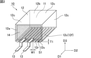
- FIG. 2 is a perspective view that typically illustrates the electronic component illustrated in FIG.
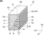
- FIG. 3 is a perspective view showing the electronic component shown in FIG. 1 as viewed in a direction different from that shown in FIG.
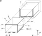
- FIG. 4 is a perspective view for explaining an example of a method for manufacturing the exterior case shown in FIG.
- FIG. 5 is a perspective view illustrating a schematic diagram of another example of the electronic component packaging structure according to the first embodiment of the present invention.
- FIG. 6 is a perspective view that typically illustrates the electronic component illustrated in FIG.
- FIG. 7 is a perspective view showing the electronic component shown in FIG. 5 as viewed in a direction different from that shown in FIG. FIG.
- FIG. 8 is a perspective view showing a schematic example of an electronic component mounting structure according to the second embodiment of the present invention.
- FIG. 9 is a perspective view that illustrates the electronic component illustrated in FIG.
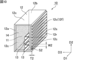
- FIG. 10 is a perspective view showing the electronic component shown in FIG. 8 as viewed from a different direction than that shown in FIG.
- the electronic component used in the electronic component mounting structure of the present invention is also one aspect of the present invention. That is, the electronic component of the present invention is an electronic component comprising an element and an exterior case in which the element is housed, the outer surface of the exterior case includes a mounting surface that faces the mounting target when the electronic component is mounted on the mounting target via an adhesive member, and the mounting surface has at least one recess for arranging the adhesive member.
- the exterior case for electronic components used in the electronic component mounting structure of the present invention is also one aspect of the present invention. That is, the exterior case for electronic components of the present invention is an exterior case for electronic components for storing elements of electronic components inside, characterized in that the outer surface of the exterior case includes a mounting surface that faces the mounting target when the electronic component is mounted on the mounting target via an adhesive member, and the mounting surface has at least one recess for arranging the adhesive member.
- the outer case is cylindrical with a bottom and an opening at one end in the first direction, and the outer surface of the outer case includes a bottom surface facing the opening in the first direction and a side surface extending in the first direction from the bottom surface toward the opening, and a portion of the side surface is the mounting surface.
- the recess extends linearly.
- FIG. 1 is a perspective view showing a schematic example of an electronic component mounting structure according to a first embodiment of the present invention.
- the electronic component mounting structure 1A shown in FIG. 1 has an electronic component 10, an object to be mounted 20, and an adhesive member 30.
- the first direction D1, the second direction D2, and the third direction D3 are perpendicular to each other.
- FIG. 2 is a perspective view that shows the electronic component shown in FIG. 1.
- FIG. 3 is a perspective view that shows the electronic component shown in FIG. 1 when viewed from a different direction than FIG. 2.
- the electronic component 10 has an element 11 and an exterior case 12.
- the type of element 11 is not particularly limited.
- Element 11 may be, for example, a capacitor.
- the type of capacitor is not particularly limited, but a film capacitor is preferable.
- the film capacitor may be a wound type film capacitor in which a metallized film is wound in a laminated state, or a laminate type film capacitor in which a metallized film is laminated.
- element 11 may be, for example, an inductor. There are no particular limitations on the type of inductor.
- the element 11 is housed inside the exterior case 12.
- the element 11 is stored inside the outer case 12 so as to be away from the inner surface of the outer case 12.
- the outer case 12 is a cylindrical shape with a bottom and an opening 12a at one end in the first direction D1.
- the outer case 12 is a rectangular cylindrical shape with a bottom.
- the outer surface of the exterior case 12 includes a bottom surface 12b facing the opening 12a in the first direction D1, and side surfaces 12c (including four surfaces in the example shown in Figures 2 and 3) extending from the bottom surface 12b toward the opening 12a in the first direction D1.
- the outer surface of the exterior case 12 includes a mounting surface 12f that faces the mounting target 20.
- the mounting surface 12f is the surface of the outer surface of the exterior case 12 that faces the mounting target 20 when the electronic component 10 is mounted on the mounting target 20 via an adhesive member 30, as described below.
- a part of the side surface 12c is the mounting surface 12f.
- At least one recess 12r is present on the mounting surface 12f. In the example shown in Figures 2 and 3, multiple recesses 12r are present on the mounting surface 12f.
- the recess 12r is a location for placing the adhesive member 30 when mounting the electronic component 10 to the mounting target 20 via the adhesive member 30, as described below.
- the recess 12r extends in the first direction D1 from the end of the mounting surface 12f on the opening 12a side to the end of the mounting surface 12f on the bottom surface 12b side. In this way, the recess 12r is groove-shaped and extends in the first direction D1.
- the recess 12r extends linearly. Specifically, the recess 12r extends linearly in the first direction D1 from the end of the mounting surface 12f on the opening 12a side to the end of the mounting surface 12f on the bottom surface 12b side.
- the cross-sectional area S1 of the recess 12r when viewed from the first direction D1 is constant regardless of the position in the first direction D1. Furthermore, the height T1 of the recess 12r in a direction perpendicular to the mounting surface 12f (third direction D3 in the example shown in Figures 2 and 3) when viewed from the first direction D1 is constant regardless of the position in the first direction D1. Therefore, the width W1 of the recess 12r in a direction parallel to the mounting surface 12f (second direction D2 in the example shown in Figures 2 and 3) when viewed from the first direction D1 is constant regardless of the position in the first direction D1.
- the multiple recesses 12r extend parallel to each other. Specifically, it is preferable that the multiple recesses 12r extend parallel to each other while extending linearly in the first direction D1 from the end of the mounting surface 12f on the opening 12a side to the end of the mounting surface 12f on the bottom surface 12b side.
- FIG. 4 is a perspective view illustrating an example of a manufacturing method for the exterior case shown in FIG. 1.
- the constituent material of the outer case 12 e.g., resin
- the constituent material of the outer case 12 e.g., resin
- the mold 40 to form the molded product, and then the molded product, the outer case 12, is removed from the mold 40.
- a recess 12r is provided so as to extend parallel to the direction in which the outer case 12 is removed, it becomes easier to remove the outer case 12 from the mold 40.
- a bottomed cylindrical outer case 12 having an opening 12a at one end in the first direction D1 as shown in Figures 2 and 3 is manufactured by, for example, injection molding
- the outer case 12 is usually removed from the mold 40 in the first direction D1 from the bottom 12b side toward the opposite side to the opening 12a. Therefore, when manufacturing the outer case 12 as shown in Figures 2 and 3 by, for example, injection molding, providing the recess 12r that extends linearly in the first direction D1 as described above makes it easier to remove the outer case 12 from the bottom surface 12b side in the first direction D1 toward the side opposite the opening 12a when removing the outer case 12 from the mold 40. As a result, the manufacturing efficiency of the outer case 12 is improved.
- protruding portions 12s On the mounting surface 12f, there are protruding portions 12s around the recessed portion 12r.
- the recessed portion 12r is located between the pair of protruding portions 12s in the second direction D2.
- protrusion 12s is integrated with the base surface.
- two elements being integrated means that there is no interface between the elements, for example, it means that the boundary between the elements cannot be distinguished.
- the protrusion 12s does not have to be integrated with the base surface.
- the protrusion 12s and the base surface may be bonded or adhered, for example, so that an interface between the two exists.
- Examples of the exterior case 12 include a resin case, a metal case, etc.
- the resin that constitutes the resin case examples include liquid crystal polymer (LCP), polyphenylene sulfide resin, polybutylene terephthalate resin, etc. Among these, it is preferable that the resin case contains a liquid crystal polymer.
- LCP liquid crystal polymer
- polyphenylene sulfide resin polyphenylene sulfide resin
- polybutylene terephthalate resin etc.
- the resin case contains a liquid crystal polymer.
- the liquid crystal polymer contained in the resin case may be, for example, a liquid crystal polymer having p-hydroxybenzoic acid and 6-hydroxy-2-naphthoic acid groups in its skeleton.
- liquid crystal polymers formed from polycondensates using various components such as phenol, phthalic acid, and ethylene terephthalate can also be used.
- Liquid crystal polymers can also be classified into types I, II, and III, but the material used is the same as the liquid crystal polymer formed from the above-mentioned components.
- the resin case preferably further contains an inorganic filler in addition to the liquid crystal polymer.
- the inorganic filler contained in the resin case can be a material that is stronger than the liquid crystal polymer.
- the inorganic filler is preferably a material that has a higher melting point than the liquid crystal polymer, and more preferably a material with a melting point of 680°C or higher.
- the shape of the inorganic filler is not particularly limited, and examples include a shape having a longitudinal direction such as a fiber shape or a plate shape.
- As an inorganic filler of such a shape multiple types of inorganic materials may be used in combination.
- the resin case contains at least one of a fibrous inorganic material and a plate-shaped inorganic material as the inorganic filler.
- a filler being fibrous means that the relationship between the longitudinal dimension in the longitudinal direction and the cross-sectional diameter in a cross section perpendicular to the longitudinal direction is longitudinal dimension/cross-sectional diameter ⁇ 5 (i.e., aspect ratio is 5:1 or more).
- the cross-sectional diameter is the longest distance between two points on the circumference of the cross section. If the cross-sectional diameter varies in the longitudinal direction, the measurement is taken at the point where the cross-sectional diameter is largest.
- a filler being plate-like means that the relationship between the cross-sectional diameter of the face with the largest projected area and the maximum height in the direction perpendicular to this cross section is cross-sectional diameter/maximum height ⁇ 3.
- the inorganic filler has a portion on the side surface 12c that is oriented in a direction from the bottom surface 12b toward the opening 12a, and a portion that is oriented in the outer circumferential direction of the side surface 12c, and is dispersed inside the exterior case 12.
- the size of the inorganic filler is preferably 5 ⁇ m or more in diameter and 50 ⁇ m or more in length.
- inorganic fillers examples include inorganic materials such as fibrous glass filler, plate-like talc or mica. Of these, it is preferable for the inorganic filler to contain fibrous glass filler as the main component.
- the resin case contains another resin (e.g., polyphenylene sulfide resin) instead of the liquid crystal polymer, it is preferable that the resin case further contains an inorganic filler as described above.
- another resin e.g., polyphenylene sulfide resin
- the resin case further contains an inorganic filler as described above.
- the resin case is manufactured by methods such as injection molding and 3D printing (three-dimensional modeling).
- the metal that constitutes the metal case include simple metals such as aluminum, magnesium, iron, stainless steel, and copper, and alloys that contain at least one of these simple metals. Of these, it is preferable that the metal case contains aluminum or an aluminum alloy.
- the metal case is manufactured by methods such as impact molding and 3D printing (three-dimensional modeling).
- the electronic component 10 preferably further has a lead terminal 13 electrically connected to an external electrode (not shown) of the element 11.
- the lead terminal 13 is used as a terminal for electrically connecting the electronic component 10 (element 11) to an external conductor (not shown) such as a bus bar or a substrate.
- the electronic component 10 has a pair of pull-out terminals 13.
- the pair of pull-out terminals 13 are electrically connected to a pair of external electrodes (not shown) of the element 11, which have mutually different polarities.
- the pair of pull-out terminals 13 have mutually different polarities.
- the lead-out terminal 13 may be connected to the external electrode of the element 11 via a joining member such as solder, or may be welded.
- the lead-out terminal 13 protrudes from the opening 12a toward the outside.
- the shape of the draw-out terminal 13 is not particularly limited.
- the draw-out terminal 13 may be, for example, plate-shaped or linear (rod-shaped).
- the draw-out terminal 13 may be, for example, partially bent or not bent.
- the constituent material of the drawer terminal 13 may be, for example, a metal such as copper, oxygen-free copper, aluminum, or an alloy containing at least one of these. Among these, the constituent material of the drawer terminal 13 is preferably copper or oxygen-free copper.
- the constituent material of the drawer terminal 13 is a copper-based material, for example, oxygen-free copper (copper: 99.96% by weight or more), tough pitch copper (copper: 99.90% by weight or more), phosphorus deoxidized copper (copper: 99.90% by weight or more, phosphorus: 0.015% by weight or more, 0.040% by weight or less), etc. can be used.
- the electronic component 10 preferably further includes a filling resin 14 that is filled inside the exterior case 12 so as to bury the element 11.
- the filling resin 14 makes it easier to hold the element 11 inside the exterior case 12.
- the filling resin 14 is filled between the element 11 and the outer case 12, specifically, between the outer surface of the element 11 and the inner surface of the outer case 12. Furthermore, it is preferable that the filling resin 14 is filled inside the outer case 12, not only between the element 11 and the outer case 12, but also in the area from the opening 12a to the element 11.
- the thickness of the filling resin 14 at the opening 12a is large.
- the thickness of the filling resin 14 at the opening 12a is preferably sufficiently large within the range that allows for the volume (physical size) of the entire electronic component 10, and specifically, is preferably 2 mm or more, and more preferably 4 mm or more.
- the element 11 is disposed closer to the bottom surface 12b than to the opening 12a inside the exterior case 12, so that the thickness of the filling resin 14 relative to the element 11 is greater on the opening 12a side than on the bottom surface 12b side.
- the thickness of the filling resin 14 is measured, for example, using a soft X-ray device if it is in a non-destructive state, and using a length measuring device such as a caliper if it is in a destructive state.
- the relationship between the height of the outer case 12 and the height of the filled resin 14 in the first direction D1 is such that the thickness of the filled resin 14 at the opening 12a is as large as possible, and it may be up to a position on the inside of the outer case 12, or it may be just about to the top, or it may overflow slightly due to surface tension.
- the filling resin 14 it is preferable to appropriately select a resin with low moisture permeability from the viewpoint of suppressing the infiltration of moisture into the element 11, and examples thereof include epoxy resin, silicone resin, urethane resin, etc.
- examples of the hardener for the epoxy resin include amine hardener, imidazole hardener, etc.
- filling resin 14 only the above-mentioned resin may be used, but in order to improve strength, a resin to which a reinforcing agent has been added may also be used.
- reinforcing agents include silica and alumina.
- the electronic component 10 is mounted on the mounting object 20. Specifically, as described below, the electronic component 10 is mounted on the mounting object 20 via an adhesive member 30.
- the shape of the mounting object 20 is not particularly limited.
- the mounting object 20 may, for example, have a partially curved shape or a non-bent shape.
- the surface of the mounting object 20 may, for example, be flat or uneven.
- Examples of the mounting object 20 include a housing, a circuit board, etc.
- examples of the mounting object 20 include die-cast products used in various automobile parts, preferably aluminum die-cast products, etc.
- the adhesive member 30 is provided between the electronic component 10 and the mounting object 20, and bonds the electronic component 10 and the mounting object 20 together.
- the adhesive material 30 penetrates into the recess 12r present on the mounting surface 12f of the exterior case 12. This increases the adhesion area between the electronic component 10 and the mounting object 20, and, combined with the anchor effect, the electronic component 10 is firmly fixed to the mounting object 20. Furthermore, the protrusion 12s acts as a barrier against the adhesive material 30 that has penetrated into the recess 12r, making it difficult for the adhesive material 30 to flow out to places other than between the electronic component 10 and the mounting object 20.
- the type of adhesive member 30 is not particularly limited as long as it is capable of adhering the electronic component 10 and the mounting object 20.
- the adhesive member 30 may be, for example, an adhesive.
- the type of adhesive is not particularly limited, and examples include adhesives containing epoxy resin.
- the electronic component mounting structure 1A makes it possible to firmly fix the electronic component 10.
- the protrusion 12s does not have to protrude beyond the side surface 12c in a direction perpendicular to the mounting surface 12f (in the example shown in Figures 2 and 3, the third direction D3). Specifically, this is as follows.
- FIG. 5 is a perspective view showing a schematic representation of another example of an electronic component mounting structure according to embodiment 1 of the present invention.
- FIG. 6 is a perspective view showing a schematic representation of the electronic component shown in FIG. 5.
- FIG. 7 is a perspective view showing a schematic representation of the electronic component shown in FIG. 5 as viewed from a different direction than in FIG. 6.
- the convex portion 12s does not protrude beyond the side surface 12c in a direction perpendicular to the mounting surface 12f (in the example shown in FIGS. 6 and 7, the third direction D3).
- the thickness of the mounting surface 12f can be increased by the amount of the convex portion 12s without increasing the overall size of the outer case 12. Therefore, in the electronic component mounting structure 1B, the strength of the outer case 12 can be improved and the outer case 12 can be made smaller.
- FIG. 8 is a perspective view that shows a schematic example of an electronic component mounting structure according to a second embodiment of the present invention.
- FIG. 9 is a perspective view that shows a schematic example of the electronic component shown in FIG. 8.
- FIG. 10 is a perspective view that shows a schematic example of the electronic component shown in FIG. 8 when viewed from a different direction than in FIG. 9.
- the cross-sectional area S2 of the recess 12r when viewed from the first direction D1 decreases from the opening 12a side toward the bottom surface 12b side.
- the height T2 of the recess 12r in the direction perpendicular to the mounting surface 12f (the third direction D3 in the example shown in FIG. 9 and FIG. 10) when viewed from the first direction D1 is constant regardless of the position in the first direction D1. Therefore, the width W2 of the recess 12r in the direction parallel to the mounting surface 12f (the second direction D2 in the example shown in FIG. 9 and FIG. 10) when viewed from the first direction D1 decreases from the opening 12a side toward the bottom surface 12b side.
- the cross-sectional area S2 of the recess 12r when viewed from the first direction D1 may gradually (continuously) decrease from the opening 12a side toward the bottom surface 12b side, or may be locally constant midway from the opening 12a side toward the bottom surface 12b side.
- the width W2 of the recess 12r in a direction parallel to the mounting surface 12f may gradually (continuously) decrease from the opening 12a side toward the bottom surface 12b side, or may be locally constant midway from the opening 12a side toward the bottom surface 12b side.
- the electronic component mounting structure of the present invention is not limited to the above embodiment, and various applications and modifications can be made within the scope of the present invention with respect to the configuration and manufacturing conditions of the electronic component mounting structure.
- the number of recesses present on the mounting surface is not particularly limited, and may be one or more.
- the shape of the recess present on the mounting surface is not particularly limited, and may be, for example, a groove shape or a shape other than a groove shape. If the recess has a shape other than a groove shape, the recess may be, for example, a hole shape.
- the shape of the recess (hole) when viewed from a direction perpendicular to the mounting surface is not particularly limited, and may be, for example, polygonal, circular, elliptical, etc.
- the recess is hole-shaped, and the exterior case is manufactured by 3D printing (three-dimensional modeling), there is no need to consider manufacturing efficiency issues such as making the exterior case easier to remove from a mold when manufacturing the exterior case by injection molding.
- the tube shape of the exterior case is not particularly limited and may be, for example, a square tube, a cylindrical shape, etc.
- the exterior case is cylindrical with a bottom
- a part of the side surface may be the mounting surface, or the bottom surface may be the mounting surface.
- the recess may be present on a part of the side surface, or on the bottom surface.
- the recess when the recess extends from one end of the mounting surface to the other end, the recess may extend linearly or in a shape other than linear. When the recess extends in a shape other than linearly, the recess may extend, for example, in a curved shape.
- the cross-sectional area of the recess when viewed in the direction in which the recess extends may or may not be constant from one end to the other end of the mounting surface. If the cross-sectional area of the recess is not constant from one end to the other end of the mounting surface, the cross-sectional area of the recess may or may not become smaller from one end to the other end of the mounting surface.
- the height of the recess in a direction perpendicular to the mounting surface when viewed from the direction in which the recess extends may or may not be constant from one end to the other end of the mounting surface. If the height of the recess is not constant from one end to the other end of the mounting surface, the height of the recess may or may not become smaller from one end to the other end of the mounting surface.
- the width of the recess in a direction parallel to the mounting surface when viewed from the direction in which the recess extends may or may not be constant from one end to the other end of the mounting surface. If the width of the recess is not constant from one end to the other end of the mounting surface, the width of the recess may or may not become smaller from one end to the other end of the mounting surface.
- the number of elements housed inside one exterior case is not particularly limited, and may be one or more.
- the electronic component mounting structure of the present invention is capable of firmly fixing electronic components, and is therefore useful, for example, in power conversion equipment for in-vehicle use that requires high resistance to vibration and shock.
- the electronic component mounting structure of the present invention is useful for motor drive inverters mounted on electric vehicles.
- the various features (e.g., preferred features) of the electronic components of the present invention are similar to the various features (e.g., preferred features) of the electronic components of the electronic component mounting structure of the present invention.
- the electronic component of the present invention is useful, for example, in power conversion devices for in-vehicle use.
- the electronic component of the present invention is useful in motor drive inverters mounted on electric vehicles.
- the electronic component exterior case of the present invention is not limited to the above embodiment, and various applications and modifications can be made within the scope of the present invention with respect to the configuration and manufacturing conditions of the electronic component exterior case.
- the various features (e.g., preferred features) of the exterior case for electronic components of the present invention are similar to the various features (e.g., preferred features) of the exterior case for electronic components of the electronic component mounting structure of the present invention.
- the electronic component exterior case of the present invention is useful for electronic components used in, for example, power conversion equipment for vehicle applications.
- the electronic component exterior case of the present invention is useful for electronic components used in motor drive inverters mounted on electric vehicles.
- the electronic component mounting structure of the present invention, the electronic component of the present invention, and the method of fixing an electronic component using the exterior case for electronic components of the present invention may also be one aspect of the present invention.
- Such a method of fixing an electronic component is characterized in that, for example, an electronic component having an element and an exterior case in which the element is housed, and having at least one recess on the mounting surface of the exterior case, is mounted on the mounting object from the mounting surface side by an adhesive member that fits into the recess between the electronic component and the mounting object.
- Electronic components a mounting target on which the electronic component is mounted; and an adhesive member provided between the electronic component and the mounting object, for adhering the electronic component and the mounting object;
- the electronic component includes an element and an exterior case in which the element is housed, an outer surface of the exterior case includes a mounting surface facing the mounting object, At least one recess is present on the mounting surface,
- the electronic component mounting structure is characterized in that the adhesive member fills the recess.
- the outer case is a bottomed cylindrical case having an opening at one end in the first direction
- the outer surface of the exterior case includes a bottom surface facing the opening in the first direction and a side surface extending in the first direction from the bottom surface toward the opening
- ⁇ 3> The electronic component mounting structure described in ⁇ 2>, wherein the recess extends in the first direction from an end of the mounting surface on the opening side to an end of the mounting surface on the bottom side.
- ⁇ 6> The electronic component mounting structure according to ⁇ 3>, wherein a cross-sectional area of the recess when viewed from the first direction decreases from the opening side toward the bottom side.
- an outer surface of the exterior case includes a mounting surface that faces the mounting object when the electronic component is mounted on the mounting object via an adhesive member;
- the electronic component is characterized in that the mounting surface has at least one recess for locating the adhesive member.
- the outer case is a bottomed cylindrical case having an opening at one end in the first direction
- the outer surface of the exterior case includes a bottom surface facing the opening in the first direction and a side surface extending in the first direction from the bottom surface toward the opening
- An exterior case for electronic components for housing elements of electronic components therein an outer surface of the exterior case includes a mounting surface that faces the mounting object when the electronic component is mounted on the mounting object via an adhesive member;
- the electronic component exterior case is characterized in that the mounting surface has at least one recess for arranging the adhesive member.
- the outer case is a bottomed cylindrical case having an opening at one end in the first direction
- the outer surface of the exterior case includes a bottom surface facing the opening in the first direction and a side surface extending in the first direction from the bottom surface toward the opening
Landscapes
- Engineering & Computer Science (AREA)
- Power Engineering (AREA)
- Microelectronics & Electronic Packaging (AREA)
- Manufacturing & Machinery (AREA)
- Casings For Electric Apparatus (AREA)
Abstract
電子部品実装構造1Aは、電子部品10と、電子部品10が実装された実装対象物20と、電子部品10と実装対象物20との間に設けられ、電子部品10及び実装対象物20を接着する接着部材30と、を備え、電子部品10が、素子11と、素子11が内部に収納された外装ケース12と、を有し、外装ケース12の外面が、実装対象物20に対向する実装面12fを含み、実装面12fには、少なくとも1つの凹部12rが存在し、接着部材30が、凹部12rに入り込んでいる。
Description
本発明は、電子部品実装構造、電子部品、及び、電子部品用外装ケースに関する。
特許文献1には、一対の外部引き出し用のリード線を有する素子を収納した有底筒状のケースと、上記素子のリード線が貫通する貫通孔を備えて上記ケースの開口部を封止した封口部材からなり、配線基板に横置き状態で実装される電子部品であって、上記ケースの底面の一部と封口部材の上面の一部に突起または窪みを設けることにより横置きにした電子部品の両端に略対称な段差を設け、この段差の境界部の面を配線基板への取り付け面とした電子部品が開示されている。
近年、自動車業界では、電気自動車、ハイブリッド自動車、燃料電池自動車等の電動車両に見られるように、自動車の電動化が進められている。自動車の電動化にともなって、自動車には、コンデンサ、インダクタ等の電子部品が多く使用される。このように車載用途で使用される電子部品には、振動、衝撃等が加わっても外れにくいといった強固な固定状態とされることが求められる。
これに対して、特許文献1に記載の電子部品では、特許文献1の図1等に示されているように、ケースの底面の一部と封口部材の上面の一部に突起または窪みを設けることにより横置きにした電子部品(コンデンサ)の両端に略対称な段差を設け、この段差の境界部の面を配線基板への取り付け面とすることにより、電子部品を配線基板に確実に固定できる、とされている。しかしながら、特許文献1に記載の電子部品では、特に、車載用途で使用される場合の振動、衝撃等に耐えられない可能性が高い。つまり、特許文献1に記載の電子部品では、特に、車載用途で使用される場合を想定すると、電子部品を配線基板に強固に固定する点で改善の余地がある。
本発明は、上記の問題を解決するためになされたものであり、電子部品の強固な固定状態を実現可能な電子部品実装構造を提供することを目的とするものである。また、本発明は、上記電子部品実装構造に使用される電子部品を提供することを目的とするものである。更に、本発明は、上記電子部品に使用される電子部品用外装ケースを提供することを目的とするものである。
本発明の電子部品実装構造は、電子部品と、上記電子部品が実装された実装対象物と、上記電子部品と上記実装対象物との間に設けられ、上記電子部品及び上記実装対象物を接着する接着部材と、を備え、上記電子部品が、素子と、上記素子が内部に収納された外装ケースと、を有し、上記外装ケースの外面が、上記実装対象物に対向する実装面を含み、上記実装面には、少なくとも1つの凹部が存在し、上記接着部材が、上記凹部に入り込んでいる、ことを特徴とする。
本発明の電子部品は、素子と、上記素子が内部に収納された外装ケースと、を備える電子部品であって、上記外装ケースの外面が、上記電子部品を実装対象物に接着部材を介して実装するときに上記実装対象物に対向する実装面を含み、上記実装面には、上記接着部材を配置するための少なくとも1つの凹部が存在している、ことを特徴とする。
本発明の電子部品用外装ケースは、電子部品の素子を内部に収納するための電子部品用外装ケースであって、上記外装ケースの外面が、上記電子部品を実装対象物に接着部材を介して実装するときに上記実装対象物に対向する実装面を含み、上記実装面には、上記接着部材を配置するための少なくとも1つの凹部が存在している、ことを特徴とする。
本発明によれば、電子部品の強固な固定状態を実現可能な電子部品実装構造を提供できる。また、本発明によれば、上記電子部品実装構造に使用される電子部品を提供できる。更に、本発明によれば、上記電子部品に使用される電子部品用外装ケースを提供できる。
以下、本発明の電子部品実装構造、本発明の電子部品、及び、本発明の電子部品用外装ケースについて説明する。なお、本発明は、以下の構成に限定されるものではなく、本発明の要旨を逸脱しない範囲において適宜変更されてもよい。また、以下において記載する個々の好ましい構成を複数組み合わせたものもまた本発明である。
以下に示す各実施形態は例示であり、異なる実施形態で示す構成の部分的な置換又は組み合わせが可能であることは言うまでもない。実施形態2以降では、実施形態1と共通の事項についての記載は省略し、異なる点を主に説明する。特に、同様の構成による同様の作用効果については、実施形態毎に逐次言及しない。
以下の説明において、各実施形態を特に区別しない場合、単に「本発明の電子部品実装構造」、「本発明の電子部品」、及び、「本発明の電子部品用外装ケース」と言う。
以下に示す図面は模式図であり、その寸法、縦横比の縮尺等は実際の製品と異なる場合がある。
本明細書中、特に断らない限り、要素間の関係性を示す用語(例えば、「平行」、「垂直」等)及び要素の形状を示す用語は、文字通りの厳密な態様のみを意味するだけではなく、実質的に同等な範囲、例えば、数%程度の差異を含む範囲も意味する。
本発明の電子部品実装構造は、電子部品と、上記電子部品が実装された実装対象物と、上記電子部品と上記実装対象物との間に設けられ、上記電子部品及び上記実装対象物を接着する接着部材と、を備え、上記電子部品が、素子と、上記素子が内部に収納された外装ケースと、を有し、上記外装ケースの外面が、上記実装対象物に対向する実装面を含み、上記実装面には、少なくとも1つの凹部が存在し、上記接着部材が、上記凹部に入り込んでいる、ことを特徴とする。
本発明の電子部品実装構造に使用される電子部品もまた、本発明の1つである。すなわち、本発明の電子部品は、素子と、上記素子が内部に収納された外装ケースと、を備える電子部品であって、上記外装ケースの外面が、上記電子部品を実装対象物に接着部材を介して実装するときに上記実装対象物に対向する実装面を含み、上記実装面には、上記接着部材を配置するための少なくとも1つの凹部が存在している、ことを特徴とする。
本発明の電子部品実装構造に使用される電子部品の外装ケースもまた、本発明の1つである。すなわち、本発明の電子部品用外装ケースは、電子部品の素子を内部に収納するための電子部品用外装ケースであって、上記外装ケースの外面が、上記電子部品を実装対象物に接着部材を介して実装するときに上記実装対象物に対向する実装面を含み、上記実装面には、上記接着部材を配置するための少なくとも1つの凹部が存在している、ことを特徴とする。
[実施形態1]
本発明の実施形態1の電子部品実装構造では、外装ケースが、第1方向における一端に開口部が設けられた有底筒状であり、外装ケースの外面が、第1方向において開口部に相対する底面と、底面から開口部に向かって第1方向に延びる側面と、を含み、側面の一部が、実装面である。
本発明の実施形態1の電子部品実装構造では、外装ケースが、第1方向における一端に開口部が設けられた有底筒状であり、外装ケースの外面が、第1方向において開口部に相対する底面と、底面から開口部に向かって第1方向に延びる側面と、を含み、側面の一部が、実装面である。
本発明の実施形態1の電子部品実装構造では、凹部が、第1方向において、実装面における開口部側の端部から、実装面における底面側の端部にわたって延びている。
本発明の実施形態1の電子部品実装構造では、凹部が、直線状に延びている。
図1は、本発明の実施形態1の電子部品実装構造の一例を模式的に示す斜視図である。
図1に示す電子部品実装構造1Aは、電子部品10と、実装対象物20と、接着部材30と、を有している。
図1等において、第1方向D1と第2方向D2と第3方向D3とは、互いに垂直の関係にある。
図2は、図1に示す電子部品を模式的に示す斜視図である。図3は、図1に示す電子部品を図2と異なる方向から見た状態を模式的に示す斜視図である。
図2及び図3に示すように、電子部品10は、素子11と、外装ケース12と、を有している。
素子11の種類は、特に限定されない。
素子11は、例えば、コンデンサであってもよい。コンデンサの種類は、特に限定されないが、フィルムコンデンサが好ましい。この場合、フィルムコンデンサは、金属化フィルムが積層された状態で巻回された巻回型のフィルムコンデンサであってもよいし、金属化フィルムが積層された積層型のフィルムコンデンサであってもよい。
素子11は、コンデンサ以外に、例えば、インダクタであってもよい。インダクタの種類は、特に限定されない。
外装ケース12の内部には、素子11が収納されている。
外装ケース12の内部には、素子11が、外装ケース12の内面から離れるように収納されていることが好ましい。
外装ケース12は、第1方向D1における一端に開口部12aが設けられた有底筒状である。図2及び図3に示す例において、外装ケース12は、有底の四角筒状である。
外装ケース12の外面は、第1方向D1において開口部12aに相対する底面12bと、底面12bから開口部12aに向かって第1方向D1に延びる側面12c(図2及び図3に示す例では、4つの面を含む)と、を含んでいる。
外装ケース12の外面は、実装対象物20に対向する実装面12fを含んでいる。具体的には、実装面12fは、外装ケース12の外面のうち、後述するように、電子部品10を実装対象物20に接着部材30を介して実装するときに実装対象物20に対向する面である。図2及び図3に示す例では、側面12cの一部(具体的には、1つの側面)が、実装面12fである。
実装面12fには、少なくとも1つの凹部12rが存在している。図2及び図3に示す例において、実装面12fには、複数の凹部12rが存在している。
凹部12rは、後述するように、電子部品10を実装対象物20に接着部材30を介して実装するときに接着部材30を配置するための箇所である。
凹部12rは、第1方向D1において、実装面12fにおける開口部12a側の端部から、実装面12fにおける底面12b側の端部にわたって延びている。このように、凹部12rは、第1方向D1に延びる溝状である。
凹部12rは、直線状に延びている。具体的には、凹部12rは、第1方向D1において、実装面12fにおける開口部12a側の端部から、実装面12fにおける底面12b側の端部にわたって、直線状に延びている。
第1方向D1から見たときの凹部12rの断面積S1は、第1方向D1での位置によらず一定である。更に、第1方向D1から見たときの、実装面12fに垂直な方向(図2及び図3に示す例では、第3方向D3)における凹部12rの高さT1は、第1方向D1での位置によらず一定である。したがって、第1方向D1から見たときの、実装面12fに平行な方向(図2及び図3に示す例では、第2方向D2)における凹部12rの幅W1は、第1方向D1での位置によらず一定である。
実装面12fに複数の凹部12rが存在している場合、複数の凹部12rは、互いに平行に延びていることが好ましい。具体的には、複数の凹部12rは、第1方向D1において、実装面12fにおける開口部12a側の端部から、実装面12fにおける底面12b側の端部にわたって、直線状に延びつつ、互いに平行に延びていることが好ましい。
図4は、図1に示す外装ケースの製造方法の一例を説明するための斜視図である。
図4に示すように、外装ケース12(特に、樹脂ケース)を、例えば、射出成形によって製造する際、外装ケース12の構成材料(例えば、樹脂)を金型40に流し込んで成形した後、その成形物である外装ケース12を金型40から取り出す。この際、外装ケース12の取り出し方向と平行に延びるように凹部12rを設けておくと、外装ケース12を金型40から取り出しやすくなる。図2及び図3に示すような、第1方向D1における一端に開口部12aが設けられた有底筒状の外装ケース12を、例えば、射出成形によって製造する場合、外装ケース12を金型40から取り出すにあたっては、通常、外装ケース12を、底面12b側から開口部12aと反対側に向かって第1方向D1に取り出す。そのため、図2及び図3に示すような外装ケース12を、例えば、射出成形によって製造する場合には、上述したような、第1方向D1において直線状に延びる凹部12rを設けておくと、外装ケース12を金型40から取り出すにあたって、外装ケース12を、底面12b側から開口部12aと反対側に向かって第1方向D1に取り出しやすくなる。以上の結果、外装ケース12の製造効率が向上する。
実装面12fにおいて、凹部12rの周囲には、凸部12sが存在している。図2及び図3に示す例において、凹部12rに対して、凹部12rが延びる第1方向D1に垂直な第2方向D2での両側には、一対の凸部12sが存在している。つまり、図2及び図3に示す例において、凹部12rは、一対の凸部12sに第2方向D2で挟まれた位置に存在している。
実装面12fにおいて、凸部12sが取り除かれた状態のベース面を想定したとき、凸部12sは、上記ベース面と一体化していることが好ましい。
本明細書中、2つの要素が一体化しているとは、要素間に界面が存在しない状態を意味し、例えば、要素間の境界を判別できない状態を意味する。
凸部12sは、上記ベース面と一体化していなくてもよい。この場合、凸部12s及び上記ベース面は、例えば、接合又は接着され、両者の界面が存在する状態であってもよい。
外装ケース12としては、例えば、樹脂ケース、金属ケース等が挙げられる。
外装ケース12が樹脂ケースである場合、樹脂ケースを構成する樹脂としては、例えば、液晶ポリマー(LCP)、ポリフェニレンサルファイド樹脂、ポリブチレンテレフタレート樹脂等が挙げられる。中でも、樹脂ケースは、液晶ポリマーを含むことが好ましい。
樹脂ケースに含まれる液晶ポリマーとしては、例えば、p-ヒドロキシ安息香酸及び6-ヒドロキシ-2-ナフトエ酸基を骨格に有する液晶ポリマーが用いられる。また、p-ヒドロキシ安息香酸及び6-ヒドロキシ-2-ナフトエ酸基以外にも、フェノール、フタル酸、エチレンテレフタレート等の各種成分を用いて、重縮合体を形成した液晶ポリマーを用いることができる。また、液晶ポリマーを分類する場合、I型、II型、III型といった分類方法もあるが、材料としては、上述した構成要素から形成した液晶ポリマーと同じ材料を意味する。
樹脂ケースは、液晶ポリマーに加えて、無機充填材を更に含むことが好ましい。
樹脂ケースに含まれる無機充填材としては、液晶ポリマーよりも強度が高い材料を用いることができる。無機充填材は、液晶ポリマーよりも融点が高い材料であることが好ましく、融点が680℃以上の材料であることがより好ましい。
無機充填材の形態としては、特に限定されず、例えば、繊維状又は板状等の長手方向を有する形態が挙げられる。このような形態の無機充填材として、複数種類の無機材料を併用してもよい。樹脂ケースは、無機充填材として、繊維状の無機材料及び板状の無機材料の少なくとも一方を含むことが好ましい。
本明細書中、充填材が繊維状であるとは、充填材において、長手方向における長手方向寸法と、長手方向に垂直な断面における断面径との関係が、長手方向寸法/断面径≧5(すなわち、アスペクト比が5:1以上)である状態を意味する。ここで、断面径は、断面の外周上において最長となる2点間距離とする。断面径が長手方向で異なる場合、断面径が最大となる箇所で測定を行う。
本明細書中、充填材が板状であるとは、充填材において、投影面積が最大となる面の断面径と、この断面に垂直な方向における最大高さとの関係が、断面径/最大高さ≧3である状態を意味する。
無機充填材は、少なくともその一部が、側面12cにおいて、底面12b側から開口部12a側に向かう方向に配向している部分と、側面12cの外周方向に配向している部分とを有し、外装ケース12の内部において分散していることが好ましい。
無機充填材のサイズは、好ましくは、直径5μm以上、長さ50μm以上のサイズである。
無機充填材は、凝集することなく、外装ケース12の全体に分散していることが好ましい。
無機充填材としては、例えば、繊維状のガラスフィラー、板状のタルク又はマイカ等の無機材料が挙げられる。中でも、無機充填材は、繊維状のガラスフィラーを主成分として含むことが好ましい。
樹脂ケースが液晶ポリマーに代えて他の樹脂(例えば、ポリフェニレンサルファイド樹脂)を含む場合においても、樹脂ケースは、上述したような無機充填材を更に含むことが好ましい。
樹脂ケースは、例えば、射出成形、3Dプリント(3次元造形)等の方法によって製造される。
外装ケース12が金属ケースである場合、金属ケースを構成する金属としては、例えば、アルミニウム、マグネシウム、鉄、ステンレス、銅等の金属単体、これらの金属単体の少なくとも1種を含有する合金等が挙げられる。中でも、金属ケースは、アルミニウム又はアルミニウム合金を含むことが好ましい。
金属ケースは、例えば、インパクト成形、3Dプリント(3次元造形)等の方法によって製造される。
電子部品10は、素子11の外部電極(図示せず)に電気的に接続された引出端子13を更に有していることが好ましい。この場合、引出端子13は、電子部品10(素子11)をバスバー、基板等の外部導体(図示せず)に電気的に接続するための端子として用いられる。
図2及び図3に示す例において、電子部品10は、一対の引出端子13を有している。図2及び図3に示す例において、一対の引出端子13は、互いに異なる極性を有する、素子11の一対の外部電極(図示せず)に電気的に接続されている。つまり、一対の引出端子13は、互いに異なる極性を有している。
引出端子13は、素子11の外部電極に対して、例えば、はんだ等の接合部材を介して接続されていてもよいし、溶接されていてもよい。
素子11が外装ケース12の内部に収納された状態で、引出端子13は、開口部12aから外部に向かって突出していることが好ましい。
引出端子13の形状は、特に限定されない。引出端子13は、例えば、板状であってもよいし、線状(棒状)であってもよい。引出端子13は、例えば、一部が屈曲した形状であってもよいし、屈曲していない形状であってもよい。
引出端子13の構成材料としては、例えば、銅、無酸素銅、アルミニウム、これらの少なくとも1種を含有する合金等の金属が挙げられる。中でも、引出端子13の構成材料は、銅又は無酸素銅であることが好ましい。引出端子13の構成材料が銅系材料である場合、例えば、無酸素銅(銅:99.96重量%以上)、タフピッチ銅(銅:99.90重量%以上)、リン脱酸銅(銅:99.90重量%以上、リン:0.015重量%以上、0.040重量%以下)等を用いることができる。
電子部品10は、素子11を埋設するように外装ケース12の内部に充填された充填樹脂14を更に有していることが好ましい。この場合、充填樹脂14によって、素子11が外装ケース12の内部に保持されやすくなる。
素子11が、外装ケース12の内面から離れるように外装ケース12の内部に収納されている場合、充填樹脂14は、素子11と外装ケース12との間、具体的には、素子11の外面と外装ケース12の内面との間に充填されていることが好ましい。更に、充填樹脂14は、外装ケース12の内部において、素子11と外装ケース12との間に加えて、開口部12aから素子11にわたる領域にも充填されていることが好ましい。
素子11への水分の浸入を抑制する観点から、開口部12aにおける充填樹脂14の厚みは大きいことが好ましい。開口部12aにおける充填樹脂14の厚みは、電子部品10全体の体積(体格)が許容される範囲で充分大きいことが好ましく、具体的には、2mm以上であることが好ましく、4mm以上であることがより好ましい。特に、外装ケース12の内部において、素子11を開口部12a側よりも底面12b側に配置することで、素子11に対する充填樹脂14の厚みを、開口部12a側において底面12b側よりも大きくすることが好ましい。
充填樹脂14の厚みは、例えば、非破壊状態であれば軟X線装置を用いて測定され、破壊状態であればノギス等の測長装置を用いて測定される。
第1方向D1における、外装ケース12の高さと充填樹脂14の高さとの関係は、開口部12aにおける充填樹脂14の厚みを可能な限り大きくするとともに、外装ケース12の内部側の位置まででもよいし、すりきり一杯程度でもよいし、表面張力でやや溢れていてもよい。
充填樹脂14としては、素子11への水分の浸入を抑制する観点から、透湿性が低い樹脂を適宜選択することが好ましく、例えば、エポキシ樹脂、シリコーン樹脂、ウレタン樹脂等が挙げられる。エポキシ樹脂の硬化剤としては、例えば、アミン硬化剤、イミダゾール硬化剤等が挙げられる。
充填樹脂14としては、上述した樹脂のみが用いられてもよいが、強度の向上を目的として、樹脂に補強剤が添加されたものが用いられてもよい。補強剤としては、例えば、シリカ、アルミナ等が挙げられる。
実装対象物20には、電子部品10が実装されている。具体的には、後述するように、実装対象物20には、電子部品10が接着部材30を介して実装されている。
実装対象物20の形状は、特に限定されない。実装対象物20は、例えば、一部が屈曲した形状であってもよいし、屈曲していない形状であってもよい。実装対象物20の表面は、例えば、平坦状であってもよいし、凹凸状であってもよい。
実装対象物20としては、例えば、筐体、基板等が挙げられる。電子部品10が車載用途で使用される場合、実装対象物20としては、例えば、各種の自動車部品で使用されるダイキャスト製品、好ましくはアルミダイキャスト製品等が挙げられる。
接着部材30は、電子部品10と実装対象物20との間に設けられ、電子部品10及び実装対象物20を接着している。
接着部材30は、電子部品10及び実装対象物20を接着するにあたって、外装ケース12の実装面12fに存在する凹部12rに入り込んでいる。これにより、電子部品10と実装対象物20との接着面積が増加するため、アンカー効果も相まって、電子部品10が実装対象物20に強固に固定される。更に、凹部12rに入り込んだ接着部材30に対して凸部12sが障壁となるため、接着部材30が、電子部品10と実装対象物20との間以外の箇所に流出しにくくなる。
接着部材30の種類は、電子部品10及び実装対象物20を接着可能なものであれば、特に限定されない。
接着部材30は、例えば、接着剤であってもよい。接着剤の種類としては、特に限定されず、例えば、エポキシ樹脂を含む接着剤等が挙げられる。
以上のように、電子部品実装構造1Aでは、電子部品10の強固な固定状態を実現可能となる。
電子部品実装構造1Aにおいて、電子部品10を実装面12fに沿う方向(図2及び図3に示す例では、第1方向D1及び第2方向D2を含む方向)から見たとき、凸部12sは、実装面12fに垂直な方向(図2及び図3に示す例では、第3方向D3)において側面12cよりも突出している。これにより、電子部品実装構造1Aでは、凸部12sが突出する分だけ外装ケース12全体のサイズが大きくなり得るものの、凸部12sの分だけ実装面12fの厚みを大きくすることができる。そのため、電子部品実装構造1Aでは、外装ケース12の強度向上が可能となる。
これに対して、電子部品10を実装面12fに沿う方向(図2及び図3に示す例では、第1方向D1及び第2方向D2を含む方向)から見たとき、凸部12sは、実装面12fに垂直な方向(図2及び図3に示す例では、第3方向D3)において側面12cよりも突出していなくてもよい。具体的には、以下の通りである。
図5は、本発明の実施形態1の電子部品実装構造の別の一例を模式的に示す斜視図である。図6は、図5に示す電子部品を模式的に示す斜視図である。図7は、図5に示す電子部品を図6と異なる方向から見た状態を模式的に示す斜視図である。
図5に示す電子部品実装構造1Bにおいて、図6及び図7にも示すように、電子部品10を実装面12fに沿う方向(図6及び図7に示す例では、第1方向D1及び第2方向D2を含む方向)から見たとき、凸部12sは、実装面12fに垂直な方向(図6及び図7に示す例では、第3方向D3)において側面12cよりも突出していない。これにより、電子部品実装構造1Bでは、凸部12sの分だけ実装面12fの厚みを大きくするにあたって、外装ケース12全体のサイズを大きくしなくてもよい。そのため、電子部品実装構造1Bでは、外装ケース12の強度向上とともに、外装ケース12の小型化も可能となる。
[実施形態2]
本発明の実施形態2の電子部品実装構造では、本発明の実施形態1の電子部品実装構造と異なり、第1方向から見たときの凹部の断面積が、開口部側から底面側に向かうにつれて小さくなる。
本発明の実施形態2の電子部品実装構造では、本発明の実施形態1の電子部品実装構造と異なり、第1方向から見たときの凹部の断面積が、開口部側から底面側に向かうにつれて小さくなる。
図8は、本発明の実施形態2の電子部品実装構造の一例を模式的に示す斜視図である。図9は、図8に示す電子部品を模式的に示す斜視図である。図10は、図8に示す電子部品を図9と異なる方向から見た状態を模式的に示す斜視図である。
図8に示す電子部品実装構造2において、図9及び図10にも示すように、第1方向D1から見たときの凹部12rの断面積S2は、開口部12a側から底面12b側に向かうにつれて小さくなる。更に、第1方向D1から見たときの、実装面12fに垂直な方向(図9及び図10に示す例では、第3方向D3)における凹部12rの高さT2は、第1方向D1での位置によらず一定である。したがって、第1方向D1から見たときの、実装面12fに平行な方向(図9及び図10に示す例では、第2方向D2)における凹部12rの幅W2は、開口部12a側から底面12b側に向かうにつれて小さくなる。
第1方向D1から見たときの凹部12rの断面積S2は、開口部12a側から底面12b側に向かうにつれて徐々に(連続的に)小さくなってもよいし、開口部12a側から底面12b側に向かう途中で局所的に一定であってもよい。
第1方向D1から見たときの、実装面12fに平行な方向(図9及び図10に示す例では、第2方向D2)における凹部12rの幅W2は、開口部12a側から底面12b側に向かうにつれて徐々に(連続的に)小さくなってもよいし、開口部12a側から底面12b側に向かう途中で局所的に一定であってもよい。
図9及び図10に示すような、第1方向D1における一端に開口部12aが設けられた有底筒状の外装ケース12を、例えば、射出成形によって製造する場合には、上述したような、開口部12a側から底面12b側に向かうにつれて断面積S2が小さくなる凹部12rを設けておくと、外装ケース12を金型から取り出すにあたって、外装ケース12を底面12b側から開口部12aと反対側に向かって第1方向D1に取り出すことが、更に容易になる。以上の結果、外装ケース12の製造効率が更に向上する。
本発明の電子部品実装構造は、上記実施形態に限定されるものではなく、電子部品実装構造の構成、製造条件等に関し、本発明の範囲内において、種々の応用、変形を加えることが可能である。
本発明の電子部品実装構造において、実装面に存在する凹部の数は、特に限定されず、1つであってもよいし、複数であってもよい。
本発明の電子部品実装構造において、実装面に存在する凹部の形状は、特に限定されず、例えば、溝状であってもよいし、溝状以外の形状であってもよい。凹部が溝状以外の形状である場合、凹部は、例えば、穴状であってもよい。
本発明の電子部品実装構造において、凹部が穴状である場合、実装面に垂直な方向から見たときの凹部(穴)の形状は、特に限定されず、例えば、多角形状、円状、楕円状等であってもよい。
本発明の電子部品実装構造において、凹部が穴状である場合、外装ケースを3Dプリント(3次元造形)によって製造すれば、外装ケースを射出成形によって製造する際に外装ケースを金型から取り出しやすくする、といった製造効率に関する点を考慮する必要がなくなる。
本発明の電子部品実装構造において、外装ケースが有底筒状である場合、外装ケースの筒形状は、特に限定されず、例えば、角筒状、円筒状等であってもよい。
本発明の電子部品実装構造において、外装ケースが有底筒状である場合、側面の一部が実装面であってもよいし、底面が実装面であってもよい。つまり、本発明の電子部品実装構造において、凹部は、側面の一部に存在していてもよいし、底面に存在していてもよい。
本発明の電子部品実装構造において、凹部が、実装面の一端から他端にわたって延びている場合、凹部は、直線状に延びていてもよいし、直線状以外の形状で延びていてもよい。凹部が直線状以外の形状で延びている場合、凹部は、例えば、曲線状に延びていてもよい。
本発明の電子部品実装構造において、凹部が、実装面の一端から他端にわたって延びている場合、凹部が延びる方向から見たときの凹部の断面積は、実装面の一端側から他端側に向かうにつれて、一定であってもよいし、一定でなくてもよい。凹部の断面積が、実装面の一端側から他端側に向かうにつれて一定でない場合、凹部の断面積は、実装面の一端側から他端側に向かうにつれて、小さくなってもよいし、大きくなってもよい。
本発明の電子部品実装構造において、凹部が、実装面の一端から他端にわたって延びている場合、凹部が延びる方向から見たときの、実装面に垂直な方向における凹部の高さは、実装面の一端側から他端側に向かうにつれて、一定であってもよいし、一定でなくてもよい。凹部の高さが、実装面の一端側から他端側に向かうにつれて一定でない場合、凹部の高さは、実装面の一端側から他端側に向かうにつれて、小さくなってもよいし、大きくなってもよい。
本発明の電子部品実装構造において、凹部が、実装面の一端から他端にわたって延びている場合、凹部が延びる方向から見たときの、実装面に平行な方向における凹部の幅は、実装面の一端側から他端側に向かうにつれて、一定であってもよいし、一定でなくてもよい。凹部の幅が、実装面の一端側から他端側に向かうにつれて一定でない場合、凹部の幅は、実装面の一端側から他端側に向かうにつれて、小さくなってもよいし、大きくなってもよい。
本発明の電子部品実装構造において、1つの外装ケースの内部に収納されている素子の数は、特に限定されず、1つであってもよいし、複数であってもよい。
本発明の電子部品実装構造は、電子部品の強固な固定状態を実現可能であるため、例えば、高い耐振動衝撃性が求められる車載用途の電力変換機器に有用である。特に、本発明の電子部品実装構造は、電動車両に搭載されるモータ駆動用インバータに有用である。
本発明の電子部品は、上記実施形態に限定されるものではなく、電子部品の構成、製造条件等に関し、本発明の範囲内において、種々の応用、変形を加えることが可能である。
本発明の電子部品に関する各種特徴(例えば、好ましい特徴)は、本発明の電子部品実装構造のうちの電子部品に関する各種特徴(例えば、好ましい特徴)と同様である。
本発明の電子部品は、例えば、車載用途の電力変換機器に有用である。特に、本発明の電子部品は、電動車両に搭載されるモータ駆動用インバータに有用である。
本発明の電子部品用外装ケースは、上記実施形態に限定されるものではなく、電子部品用外装ケースの構成、製造条件等に関し、本発明の範囲内において、種々の応用、変形を加えることが可能である。
本発明の電子部品用外装ケースに関する各種特徴(例えば、好ましい特徴)は、本発明の電子部品実装構造のうちの電子部品用外装ケースに関する各種特徴(例えば、好ましい特徴)と同様である。
本発明の電子部品用外装ケースは、例えば、車載用途の電力変換機器に使用される電子部品に有用である。特に、本発明の電子部品用外装ケースは、電動車両に搭載されるモータ駆動用インバータに使用される電子部品に有用である。
本発明の電子部品実装構造、本発明の電子部品、及び、本発明の電子部品用外装ケースを用いて電子部品を固定する、という電子部品の固定方法もまた、本発明の1つであってもよい。このような電子部品の固定方法は、例えば、素子と、素子が内部に収納された外装ケースと、を有し、外装ケースの実装面に少なくとも1つの凹部が存在する電子部品を、電子部品と実装対象物との間で凹部に入り込む接着部材によって、実装面側から実装対象物に実装する、ことを特徴とする。
本明細書には、以下の内容が開示されている。
<1>
電子部品と、
上記電子部品が実装された実装対象物と、
上記電子部品と上記実装対象物との間に設けられ、上記電子部品及び上記実装対象物を接着する接着部材と、を備え、
上記電子部品が、素子と、上記素子が内部に収納された外装ケースと、を有し、
上記外装ケースの外面が、上記実装対象物に対向する実装面を含み、
上記実装面には、少なくとも1つの凹部が存在し、
上記接着部材が、上記凹部に入り込んでいる、ことを特徴とする電子部品実装構造。
電子部品と、
上記電子部品が実装された実装対象物と、
上記電子部品と上記実装対象物との間に設けられ、上記電子部品及び上記実装対象物を接着する接着部材と、を備え、
上記電子部品が、素子と、上記素子が内部に収納された外装ケースと、を有し、
上記外装ケースの外面が、上記実装対象物に対向する実装面を含み、
上記実装面には、少なくとも1つの凹部が存在し、
上記接着部材が、上記凹部に入り込んでいる、ことを特徴とする電子部品実装構造。
<2>
上記外装ケースが、第1方向における一端に開口部が設けられた有底筒状であり、
上記外装ケースの上記外面が、上記第1方向において上記開口部に相対する底面と、上記底面から上記開口部に向かって上記第1方向に延びる側面と、を含み、
上記側面の一部が、上記実装面である、<1>に記載の電子部品実装構造。
上記外装ケースが、第1方向における一端に開口部が設けられた有底筒状であり、
上記外装ケースの上記外面が、上記第1方向において上記開口部に相対する底面と、上記底面から上記開口部に向かって上記第1方向に延びる側面と、を含み、
上記側面の一部が、上記実装面である、<1>に記載の電子部品実装構造。
<3>
上記凹部が、上記第1方向において、上記実装面における上記開口部側の端部から、上記実装面における上記底面側の端部にわたって延びている、<2>に記載の電子部品実装構造。
上記凹部が、上記第1方向において、上記実装面における上記開口部側の端部から、上記実装面における上記底面側の端部にわたって延びている、<2>に記載の電子部品実装構造。
<4>
上記凹部が、直線状に延びている、<3>に記載の電子部品実装構造。
上記凹部が、直線状に延びている、<3>に記載の電子部品実装構造。
<5>
複数の上記凹部が、互いに平行に延びている、<4>に記載の電子部品実装構造。
複数の上記凹部が、互いに平行に延びている、<4>に記載の電子部品実装構造。
<6>
上記第1方向から見たときの上記凹部の断面積が、上記開口部側から上記底面側に向かうにつれて小さくなる、<3>に記載の電子部品実装構造。
上記第1方向から見たときの上記凹部の断面積が、上記開口部側から上記底面側に向かうにつれて小さくなる、<3>に記載の電子部品実装構造。
<7>
素子と、
上記素子が内部に収納された外装ケースと、を備える電子部品であって、
上記外装ケースの外面が、上記電子部品を実装対象物に接着部材を介して実装するときに上記実装対象物に対向する実装面を含み、
上記実装面には、上記接着部材を配置するための少なくとも1つの凹部が存在している、ことを特徴とする電子部品。
素子と、
上記素子が内部に収納された外装ケースと、を備える電子部品であって、
上記外装ケースの外面が、上記電子部品を実装対象物に接着部材を介して実装するときに上記実装対象物に対向する実装面を含み、
上記実装面には、上記接着部材を配置するための少なくとも1つの凹部が存在している、ことを特徴とする電子部品。
<8>
上記外装ケースが、第1方向における一端に開口部が設けられた有底筒状であり、
上記外装ケースの上記外面が、上記第1方向において上記開口部に相対する底面と、上記底面から上記開口部に向かって上記第1方向に延びる側面と、を含み、
上記側面の一部が、上記実装面である、<7>に記載の電子部品。
上記外装ケースが、第1方向における一端に開口部が設けられた有底筒状であり、
上記外装ケースの上記外面が、上記第1方向において上記開口部に相対する底面と、上記底面から上記開口部に向かって上記第1方向に延びる側面と、を含み、
上記側面の一部が、上記実装面である、<7>に記載の電子部品。
<9>
上記凹部が、上記第1方向において、上記実装面における上記開口部側の端部から、上記実装面における上記底面側の端部にわたって延びている、<8>に記載の電子部品。
上記凹部が、上記第1方向において、上記実装面における上記開口部側の端部から、上記実装面における上記底面側の端部にわたって延びている、<8>に記載の電子部品。
<10>
上記凹部が、直線状に延びている、<9>に記載の電子部品。
上記凹部が、直線状に延びている、<9>に記載の電子部品。
<11>
複数の上記凹部が、互いに平行に延びている、<10>に記載の電子部品。
複数の上記凹部が、互いに平行に延びている、<10>に記載の電子部品。
<12>
上記第1方向から見たときの上記凹部の断面積が、上記開口部側から上記底面側に向かうにつれて小さくなる、<9>に記載の電子部品。
上記第1方向から見たときの上記凹部の断面積が、上記開口部側から上記底面側に向かうにつれて小さくなる、<9>に記載の電子部品。
<13>
電子部品の素子を内部に収納するための電子部品用外装ケースであって、
上記外装ケースの外面が、上記電子部品を実装対象物に接着部材を介して実装するときに上記実装対象物に対向する実装面を含み、
上記実装面には、上記接着部材を配置するための少なくとも1つの凹部が存在している、ことを特徴とする電子部品用外装ケース。
電子部品の素子を内部に収納するための電子部品用外装ケースであって、
上記外装ケースの外面が、上記電子部品を実装対象物に接着部材を介して実装するときに上記実装対象物に対向する実装面を含み、
上記実装面には、上記接着部材を配置するための少なくとも1つの凹部が存在している、ことを特徴とする電子部品用外装ケース。
<14>
上記外装ケースが、第1方向における一端に開口部が設けられた有底筒状であり、
上記外装ケースの上記外面が、上記第1方向において上記開口部に相対する底面と、上記底面から上記開口部に向かって上記第1方向に延びる側面と、を含み、
上記側面の一部が、上記実装面である、<13>に記載の電子部品用外装ケース。
上記外装ケースが、第1方向における一端に開口部が設けられた有底筒状であり、
上記外装ケースの上記外面が、上記第1方向において上記開口部に相対する底面と、上記底面から上記開口部に向かって上記第1方向に延びる側面と、を含み、
上記側面の一部が、上記実装面である、<13>に記載の電子部品用外装ケース。
<15>
上記凹部が、上記第1方向において、上記実装面における上記開口部側の端部から、上記実装面における上記底面側の端部にわたって延びている、<14>に記載の電子部品用外装ケース。
上記凹部が、上記第1方向において、上記実装面における上記開口部側の端部から、上記実装面における上記底面側の端部にわたって延びている、<14>に記載の電子部品用外装ケース。
<16>
上記凹部が、直線状に延びている、<15>に記載の電子部品用外装ケース。
上記凹部が、直線状に延びている、<15>に記載の電子部品用外装ケース。
<17>
複数の上記凹部が、互いに平行に延びている、<16>に記載の電子部品用外装ケース。
複数の上記凹部が、互いに平行に延びている、<16>に記載の電子部品用外装ケース。
<18>
上記第1方向から見たときの上記凹部の断面積が、上記開口部側から上記底面側に向かうにつれて小さくなる、<15>に記載の電子部品用外装ケース。
上記第1方向から見たときの上記凹部の断面積が、上記開口部側から上記底面側に向かうにつれて小さくなる、<15>に記載の電子部品用外装ケース。
1A、1B、2 電子部品実装構造
10 電子部品
11 素子
12 外装ケース
12a 開口部
12b 底面
12c 側面
12f 実装面
12r 凹部
12s 凸部
13 引出端子
14 充填樹脂
20 実装対象物
30 接着部材
40 金型
D1 第1方向
D2 第2方向
D3 第3方向
S1、S2 凹部の断面積
T1、T2 凹部の高さ
W1、W2 凹部の幅
10 電子部品
11 素子
12 外装ケース
12a 開口部
12b 底面
12c 側面
12f 実装面
12r 凹部
12s 凸部
13 引出端子
14 充填樹脂
20 実装対象物
30 接着部材
40 金型
D1 第1方向
D2 第2方向
D3 第3方向
S1、S2 凹部の断面積
T1、T2 凹部の高さ
W1、W2 凹部の幅
Claims (18)
- 電子部品と、
前記電子部品が実装された実装対象物と、
前記電子部品と前記実装対象物との間に設けられ、前記電子部品及び前記実装対象物を接着する接着部材と、を備え、
前記電子部品が、素子と、前記素子が内部に収納された外装ケースと、を有し、
前記外装ケースの外面が、前記実装対象物に対向する実装面を含み、
前記実装面には、少なくとも1つの凹部が存在し、
前記接着部材が、前記凹部に入り込んでいる、ことを特徴とする電子部品実装構造。 - 前記外装ケースが、第1方向における一端に開口部が設けられた有底筒状であり、
前記外装ケースの前記外面が、前記第1方向において前記開口部に相対する底面と、前記底面から前記開口部に向かって前記第1方向に延びる側面と、を含み、
前記側面の一部が、前記実装面である、請求項1に記載の電子部品実装構造。 - 前記凹部が、前記第1方向において、前記実装面における前記開口部側の端部から、前記実装面における前記底面側の端部にわたって延びている、請求項2に記載の電子部品実装構造。
- 前記凹部が、直線状に延びている、請求項3に記載の電子部品実装構造。
- 複数の前記凹部が、互いに平行に延びている、請求項4に記載の電子部品実装構造。
- 前記第1方向から見たときの前記凹部の断面積が、前記開口部側から前記底面側に向かうにつれて小さくなる、請求項3に記載の電子部品実装構造。
- 素子と、
前記素子が内部に収納された外装ケースと、を備える電子部品であって、
前記外装ケースの外面が、前記電子部品を実装対象物に接着部材を介して実装するときに前記実装対象物に対向する実装面を含み、
前記実装面には、前記接着部材を配置するための少なくとも1つの凹部が存在している、ことを特徴とする電子部品。 - 前記外装ケースが、第1方向における一端に開口部が設けられた有底筒状であり、
前記外装ケースの前記外面が、前記第1方向において前記開口部に相対する底面と、前記底面から前記開口部に向かって前記第1方向に延びる側面と、を含み、
前記側面の一部が、前記実装面である、請求項7に記載の電子部品。 - 前記凹部が、前記第1方向において、前記実装面における前記開口部側の端部から、前記実装面における前記底面側の端部にわたって延びている、請求項8に記載の電子部品。
- 前記凹部が、直線状に延びている、請求項9に記載の電子部品。
- 複数の前記凹部が、互いに平行に延びている、請求項10に記載の電子部品。
- 前記第1方向から見たときの前記凹部の断面積が、前記開口部側から前記底面側に向かうにつれて小さくなる、請求項9に記載の電子部品。
- 電子部品の素子を内部に収納するための電子部品用外装ケースであって、
前記外装ケースの外面が、前記電子部品を実装対象物に接着部材を介して実装するときに前記実装対象物に対向する実装面を含み、
前記実装面には、前記接着部材を配置するための少なくとも1つの凹部が存在している、ことを特徴とする電子部品用外装ケース。 - 前記外装ケースが、第1方向における一端に開口部が設けられた有底筒状であり、
前記外装ケースの前記外面が、前記第1方向において前記開口部に相対する底面と、前記底面から前記開口部に向かって前記第1方向に延びる側面と、を含み、
前記側面の一部が、前記実装面である、請求項13に記載の電子部品用外装ケース。 - 前記凹部が、前記第1方向において、前記実装面における前記開口部側の端部から、前記実装面における前記底面側の端部にわたって延びている、請求項14に記載の電子部品用外装ケース。
- 前記凹部が、直線状に延びている、請求項15に記載の電子部品用外装ケース。
- 複数の前記凹部が、互いに平行に延びている、請求項16に記載の電子部品用外装ケース。
- 前記第1方向から見たときの前記凹部の断面積が、前記開口部側から前記底面側に向かうにつれて小さくなる、請求項15に記載の電子部品用外装ケース。
Applications Claiming Priority (2)
| Application Number | Priority Date | Filing Date | Title |
|---|---|---|---|
| JP2023-190050 | 2023-11-07 | ||
| JP2023190050 | 2023-11-07 |
Publications (1)
| Publication Number | Publication Date |
|---|---|
| WO2025100175A1 true WO2025100175A1 (ja) | 2025-05-15 |
Family
ID=95695812
Family Applications (1)
| Application Number | Title | Priority Date | Filing Date |
|---|---|---|---|
| PCT/JP2024/036677 Pending WO2025100175A1 (ja) | 2023-11-07 | 2024-10-15 | 電子部品実装構造、電子部品、及び、電子部品用外装ケース |
Country Status (1)
| Country | Link |
|---|---|
| WO (1) | WO2025100175A1 (ja) |
Citations (7)
| Publication number | Priority date | Publication date | Assignee | Title |
|---|---|---|---|---|
| JPS57104565U (ja) * | 1980-12-18 | 1982-06-28 | ||
| JPS57135764U (ja) * | 1981-02-20 | 1982-08-24 | ||
| JPH0711790U (ja) * | 1993-07-19 | 1995-02-21 | 株式会社共理関西 | リード付き部品の表面実装用変換アダプタ |
| JPH11150036A (ja) * | 1997-11-14 | 1999-06-02 | Nippon Chemicon Corp | チップ形コンデンサ |
| JP2000208356A (ja) * | 1999-01-14 | 2000-07-28 | Matsushita Electric Ind Co Ltd | 電子部品およびこれを実装する配線基板 |
| JP2017005116A (ja) * | 2015-06-10 | 2017-01-05 | トヨタ自動車株式会社 | 部品ケースの固定構造 |
| WO2020166170A1 (ja) * | 2019-02-13 | 2020-08-20 | 株式会社指月電機製作所 | フィルムコンデンサ、及び、フィルムコンデンサ用の外装ケース |
-
2024
- 2024-10-15 WO PCT/JP2024/036677 patent/WO2025100175A1/ja active Pending
Patent Citations (7)
| Publication number | Priority date | Publication date | Assignee | Title |
|---|---|---|---|---|
| JPS57104565U (ja) * | 1980-12-18 | 1982-06-28 | ||
| JPS57135764U (ja) * | 1981-02-20 | 1982-08-24 | ||
| JPH0711790U (ja) * | 1993-07-19 | 1995-02-21 | 株式会社共理関西 | リード付き部品の表面実装用変換アダプタ |
| JPH11150036A (ja) * | 1997-11-14 | 1999-06-02 | Nippon Chemicon Corp | チップ形コンデンサ |
| JP2000208356A (ja) * | 1999-01-14 | 2000-07-28 | Matsushita Electric Ind Co Ltd | 電子部品およびこれを実装する配線基板 |
| JP2017005116A (ja) * | 2015-06-10 | 2017-01-05 | トヨタ自動車株式会社 | 部品ケースの固定構造 |
| WO2020166170A1 (ja) * | 2019-02-13 | 2020-08-20 | 株式会社指月電機製作所 | フィルムコンデンサ、及び、フィルムコンデンサ用の外装ケース |
Similar Documents
| Publication | Publication Date | Title |
|---|---|---|
| JP4894427B2 (ja) | ケースモールド型コンデンサ | |
| CN116075911B (zh) | 电容器 | |
| CN111902961B (zh) | 蓄电模块 | |
| JP5796155B2 (ja) | ケースモールド型コンデンサ | |
| US20200279690A1 (en) | Capacitor | |
| JP2012199350A (ja) | ケースモールド型コンデンサ | |
| TWI683328B (zh) | 電子零件及其製造方法 | |
| JP4983217B2 (ja) | ケースモールド型コンデンサ | |
| JP7794316B2 (ja) | コンデンサ、コンデンサバンク、及び、コンデンサ用外装ケース | |
| US20220158394A1 (en) | In-vehicle electrical device | |
| WO2025100174A1 (ja) | 電子部品実装構造 | |
| WO2025047126A1 (ja) | コンデンサモジュール | |
| WO2024080021A1 (ja) | コンデンサ、コンデンサバンク、及び、コンデンサ用外装ケース | |
| JP6145690B2 (ja) | ケースモールド型コンデンサ | |
| JP6082180B2 (ja) | 車両用電子式モジュール | |
| JP2022014162A (ja) | 複合材構造及び複合材構造製造方法 | |
| JP2026068219A (ja) | コンデンサモジュール | |
| JP7698692B2 (ja) | コンデンサ | |
| JP2026068220A (ja) | コンデンサモジュール | |
| JP2026068218A (ja) | コンデンサモジュール | |
| JP2012243931A (ja) | 電子部品収納用樹脂ケース及びこれを用いたケースモールド型コンデンサ | |
| US20260058057A1 (en) | Capacitor and method for manufacturing capacitor | |
| WO2025047029A1 (ja) | コンデンサ | |
| JP2013077832A (ja) | ケースモールド型コンデンサ | |
| WO2025047116A1 (ja) | コンデンサモジュール |
Legal Events
| Date | Code | Title | Description |
|---|---|---|---|
| 121 | Ep: the epo has been informed by wipo that ep was designated in this application |
Ref document number: 24888473 Country of ref document: EP Kind code of ref document: A1 |