WO2025100069A1 - 表示デバイス - Google Patents
表示デバイス Download PDFInfo
- Publication number
- WO2025100069A1 WO2025100069A1 PCT/JP2024/031712 JP2024031712W WO2025100069A1 WO 2025100069 A1 WO2025100069 A1 WO 2025100069A1 JP 2024031712 W JP2024031712 W JP 2024031712W WO 2025100069 A1 WO2025100069 A1 WO 2025100069A1
- Authority
- WO
- WIPO (PCT)
- Prior art keywords
- light
- emitting layer
- layer
- display device
- emitting
- Prior art date
- Legal status (The legal status is an assumption and is not a legal conclusion. Google has not performed a legal analysis and makes no representation as to the accuracy of the status listed.)
- Pending
Links
Images


Classifications
-
- F—MECHANICAL ENGINEERING; LIGHTING; HEATING; WEAPONS; BLASTING
- F21—LIGHTING
- F21S—NON-PORTABLE LIGHTING DEVICES; SYSTEMS THEREOF; VEHICLE LIGHTING DEVICES SPECIALLY ADAPTED FOR VEHICLE EXTERIORS
- F21S2/00—Systems of lighting devices, not provided for in main groups F21S4/00 - F21S10/00 or F21S19/00, e.g. of modular construction
-
- G—PHYSICS
- G02—OPTICS
- G02F—OPTICAL DEVICES OR ARRANGEMENTS FOR THE CONTROL OF LIGHT BY MODIFICATION OF THE OPTICAL PROPERTIES OF THE MEDIA OF THE ELEMENTS INVOLVED THEREIN; NON-LINEAR OPTICS; FREQUENCY-CHANGING OF LIGHT; OPTICAL LOGIC ELEMENTS; OPTICAL ANALOGUE/DIGITAL CONVERTERS
- G02F1/00—Devices or arrangements for the control of the intensity, colour, phase, polarisation or direction of light arriving from an independent light source, e.g. switching, gating or modulating; Non-linear optics
- G02F1/01—Devices or arrangements for the control of the intensity, colour, phase, polarisation or direction of light arriving from an independent light source, e.g. switching, gating or modulating; Non-linear optics for the control of the intensity, phase, polarisation or colour
- G02F1/13—Devices or arrangements for the control of the intensity, colour, phase, polarisation or direction of light arriving from an independent light source, e.g. switching, gating or modulating; Non-linear optics for the control of the intensity, phase, polarisation or colour based on liquid crystals, e.g. single liquid crystal display cells
- G02F1/133—Constructional arrangements; Operation of liquid crystal cells; Circuit arrangements
-
- G—PHYSICS
- G02—OPTICS
- G02F—OPTICAL DEVICES OR ARRANGEMENTS FOR THE CONTROL OF LIGHT BY MODIFICATION OF THE OPTICAL PROPERTIES OF THE MEDIA OF THE ELEMENTS INVOLVED THEREIN; NON-LINEAR OPTICS; FREQUENCY-CHANGING OF LIGHT; OPTICAL LOGIC ELEMENTS; OPTICAL ANALOGUE/DIGITAL CONVERTERS
- G02F1/00—Devices or arrangements for the control of the intensity, colour, phase, polarisation or direction of light arriving from an independent light source, e.g. switching, gating or modulating; Non-linear optics
- G02F1/01—Devices or arrangements for the control of the intensity, colour, phase, polarisation or direction of light arriving from an independent light source, e.g. switching, gating or modulating; Non-linear optics for the control of the intensity, phase, polarisation or colour
- G02F1/13—Devices or arrangements for the control of the intensity, colour, phase, polarisation or direction of light arriving from an independent light source, e.g. switching, gating or modulating; Non-linear optics for the control of the intensity, phase, polarisation or colour based on liquid crystals, e.g. single liquid crystal display cells
- G02F1/133—Constructional arrangements; Operation of liquid crystal cells; Circuit arrangements
- G02F1/1333—Constructional arrangements; Manufacturing methods
- G02F1/1335—Structural association of cells with optical devices, e.g. polarisers or reflectors
-
- G—PHYSICS
- G02—OPTICS
- G02F—OPTICAL DEVICES OR ARRANGEMENTS FOR THE CONTROL OF LIGHT BY MODIFICATION OF THE OPTICAL PROPERTIES OF THE MEDIA OF THE ELEMENTS INVOLVED THEREIN; NON-LINEAR OPTICS; FREQUENCY-CHANGING OF LIGHT; OPTICAL LOGIC ELEMENTS; OPTICAL ANALOGUE/DIGITAL CONVERTERS
- G02F1/00—Devices or arrangements for the control of the intensity, colour, phase, polarisation or direction of light arriving from an independent light source, e.g. switching, gating or modulating; Non-linear optics
- G02F1/01—Devices or arrangements for the control of the intensity, colour, phase, polarisation or direction of light arriving from an independent light source, e.g. switching, gating or modulating; Non-linear optics for the control of the intensity, phase, polarisation or colour
- G02F1/13—Devices or arrangements for the control of the intensity, colour, phase, polarisation or direction of light arriving from an independent light source, e.g. switching, gating or modulating; Non-linear optics for the control of the intensity, phase, polarisation or colour based on liquid crystals, e.g. single liquid crystal display cells
- G02F1/133—Constructional arrangements; Operation of liquid crystal cells; Circuit arrangements
- G02F1/1333—Constructional arrangements; Manufacturing methods
- G02F1/1335—Structural association of cells with optical devices, e.g. polarisers or reflectors
- G02F1/1336—Illuminating devices
-
- G—PHYSICS
- G09—EDUCATION; CRYPTOGRAPHY; DISPLAY; ADVERTISING; SEALS
- G09F—DISPLAYING; ADVERTISING; SIGNS; LABELS OR NAME-PLATES; SEALS
- G09F9/00—Indicating arrangements for variable information in which the information is built-up on a support by selection or combination of individual elements
-
- G—PHYSICS
- G09—EDUCATION; CRYPTOGRAPHY; DISPLAY; ADVERTISING; SEALS
- G09F—DISPLAYING; ADVERTISING; SIGNS; LABELS OR NAME-PLATES; SEALS
- G09F9/00—Indicating arrangements for variable information in which the information is built-up on a support by selection or combination of individual elements
- G09F9/30—Indicating arrangements for variable information in which the information is built-up on a support by selection or combination of individual elements in which the desired character or characters are formed by combining individual elements
-
- G—PHYSICS
- G09—EDUCATION; CRYPTOGRAPHY; DISPLAY; ADVERTISING; SEALS
- G09F—DISPLAYING; ADVERTISING; SIGNS; LABELS OR NAME-PLATES; SEALS
- G09F9/00—Indicating arrangements for variable information in which the information is built-up on a support by selection or combination of individual elements
- G09F9/30—Indicating arrangements for variable information in which the information is built-up on a support by selection or combination of individual elements in which the desired character or characters are formed by combining individual elements
- G09F9/35—Indicating arrangements for variable information in which the information is built-up on a support by selection or combination of individual elements in which the desired character or characters are formed by combining individual elements being liquid crystals
-
- G—PHYSICS
- G09—EDUCATION; CRYPTOGRAPHY; DISPLAY; ADVERTISING; SEALS
- G09F—DISPLAYING; ADVERTISING; SIGNS; LABELS OR NAME-PLATES; SEALS
- G09F9/00—Indicating arrangements for variable information in which the information is built-up on a support by selection or combination of individual elements
- G09F9/46—Indicating arrangements for variable information in which the information is built-up on a support by selection or combination of individual elements in which the desired character is selected from a number of characters arranged one behind the other
-
- G—PHYSICS
- G09—EDUCATION; CRYPTOGRAPHY; DISPLAY; ADVERTISING; SEALS
- G09G—ARRANGEMENTS OR CIRCUITS FOR CONTROL OF INDICATING DEVICES USING STATIC MEANS TO PRESENT VARIABLE INFORMATION
- G09G3/00—Control arrangements or circuits, of interest only in connection with visual indicators other than cathode-ray tubes
- G09G3/20—Control arrangements or circuits, of interest only in connection with visual indicators other than cathode-ray tubes for presentation of an assembly of a number of characters, e.g. a page, by composing the assembly by combination of individual elements arranged in a matrix no fixed position being assigned to or needed to be assigned to the individual characters or partial characters
-
- G—PHYSICS
- G09—EDUCATION; CRYPTOGRAPHY; DISPLAY; ADVERTISING; SEALS
- G09G—ARRANGEMENTS OR CIRCUITS FOR CONTROL OF INDICATING DEVICES USING STATIC MEANS TO PRESENT VARIABLE INFORMATION
- G09G3/00—Control arrangements or circuits, of interest only in connection with visual indicators other than cathode-ray tubes
- G09G3/20—Control arrangements or circuits, of interest only in connection with visual indicators other than cathode-ray tubes for presentation of an assembly of a number of characters, e.g. a page, by composing the assembly by combination of individual elements arranged in a matrix no fixed position being assigned to or needed to be assigned to the individual characters or partial characters
- G09G3/22—Control arrangements or circuits, of interest only in connection with visual indicators other than cathode-ray tubes for presentation of an assembly of a number of characters, e.g. a page, by composing the assembly by combination of individual elements arranged in a matrix no fixed position being assigned to or needed to be assigned to the individual characters or partial characters using controlled light sources
- G09G3/30—Control arrangements or circuits, of interest only in connection with visual indicators other than cathode-ray tubes for presentation of an assembly of a number of characters, e.g. a page, by composing the assembly by combination of individual elements arranged in a matrix no fixed position being assigned to or needed to be assigned to the individual characters or partial characters using controlled light sources using electroluminescent panels
- G09G3/32—Control arrangements or circuits, of interest only in connection with visual indicators other than cathode-ray tubes for presentation of an assembly of a number of characters, e.g. a page, by composing the assembly by combination of individual elements arranged in a matrix no fixed position being assigned to or needed to be assigned to the individual characters or partial characters using controlled light sources using electroluminescent panels semiconductive, e.g. using light-emitting diodes [LED]
- G09G3/3208—Control arrangements or circuits, of interest only in connection with visual indicators other than cathode-ray tubes for presentation of an assembly of a number of characters, e.g. a page, by composing the assembly by combination of individual elements arranged in a matrix no fixed position being assigned to or needed to be assigned to the individual characters or partial characters using controlled light sources using electroluminescent panels semiconductive, e.g. using light-emitting diodes [LED] organic, e.g. using organic light-emitting diodes [OLED]
- G09G3/3225—Control arrangements or circuits, of interest only in connection with visual indicators other than cathode-ray tubes for presentation of an assembly of a number of characters, e.g. a page, by composing the assembly by combination of individual elements arranged in a matrix no fixed position being assigned to or needed to be assigned to the individual characters or partial characters using controlled light sources using electroluminescent panels semiconductive, e.g. using light-emitting diodes [LED] organic, e.g. using organic light-emitting diodes [OLED] using an active matrix
-
- G—PHYSICS
- G09—EDUCATION; CRYPTOGRAPHY; DISPLAY; ADVERTISING; SEALS
- G09G—ARRANGEMENTS OR CIRCUITS FOR CONTROL OF INDICATING DEVICES USING STATIC MEANS TO PRESENT VARIABLE INFORMATION
- G09G3/00—Control arrangements or circuits, of interest only in connection with visual indicators other than cathode-ray tubes
- G09G3/20—Control arrangements or circuits, of interest only in connection with visual indicators other than cathode-ray tubes for presentation of an assembly of a number of characters, e.g. a page, by composing the assembly by combination of individual elements arranged in a matrix no fixed position being assigned to or needed to be assigned to the individual characters or partial characters
- G09G3/34—Control arrangements or circuits, of interest only in connection with visual indicators other than cathode-ray tubes for presentation of an assembly of a number of characters, e.g. a page, by composing the assembly by combination of individual elements arranged in a matrix no fixed position being assigned to or needed to be assigned to the individual characters or partial characters by control of light from an independent source
-
- G—PHYSICS
- G09—EDUCATION; CRYPTOGRAPHY; DISPLAY; ADVERTISING; SEALS
- G09G—ARRANGEMENTS OR CIRCUITS FOR CONTROL OF INDICATING DEVICES USING STATIC MEANS TO PRESENT VARIABLE INFORMATION
- G09G3/00—Control arrangements or circuits, of interest only in connection with visual indicators other than cathode-ray tubes
- G09G3/20—Control arrangements or circuits, of interest only in connection with visual indicators other than cathode-ray tubes for presentation of an assembly of a number of characters, e.g. a page, by composing the assembly by combination of individual elements arranged in a matrix no fixed position being assigned to or needed to be assigned to the individual characters or partial characters
- G09G3/34—Control arrangements or circuits, of interest only in connection with visual indicators other than cathode-ray tubes for presentation of an assembly of a number of characters, e.g. a page, by composing the assembly by combination of individual elements arranged in a matrix no fixed position being assigned to or needed to be assigned to the individual characters or partial characters by control of light from an independent source
- G09G3/36—Control arrangements or circuits, of interest only in connection with visual indicators other than cathode-ray tubes for presentation of an assembly of a number of characters, e.g. a page, by composing the assembly by combination of individual elements arranged in a matrix no fixed position being assigned to or needed to be assigned to the individual characters or partial characters by control of light from an independent source using liquid crystals
-
- H—ELECTRICITY
- H10—SEMICONDUCTOR DEVICES; ELECTRIC SOLID-STATE DEVICES NOT OTHERWISE PROVIDED FOR
- H10K—ORGANIC ELECTRIC SOLID-STATE DEVICES
- H10K59/00—Integrated devices, or assemblies of multiple devices, comprising at least one organic light-emitting element covered by group H10K50/00
- H10K59/50—OLEDs integrated with light modulating elements, e.g. with electrochromic elements, photochromic elements or liquid crystal elements
Definitions
- the present invention relates to a display device.
- an organic EL display which is a type of display device
- images and the like are displayed by the self-illumination of light-emitting elements composed of OLEDs (organic light-emitting diodes).
- a backlight composed of light-emitting elements is provided on the rear surface of the liquid crystal layer and illuminates the liquid crystal layer to display images and the like.
- Liquid crystal display devices that are provided with a phosphorescent layer to supplement the emission of the backlight are also known (see, for example, Patent Document 1).
- the present invention was made in consideration of the above problems, and aims to provide a display device that can improve visibility and reduce power consumption depending on the illuminance of external light.
- a display device includes a first light-emitting layer that emits light in a first direction, which is the direction in which the display surface is facing; a phosphorescent layer that is provided on the second direction side of the first light-emitting layer and stores light received from the first direction side, the second direction being the opposite direction to the first direction; and a second light-emitting layer that is provided between the first light-emitting layer and the phosphorescent layer and emits light toward the phosphorescent layer, the power consumption of the second light-emitting layer being lower than the power consumption of the first light-emitting layer, and the phosphorescent layer stores light from at least the second light-emitting layer and emits light in the first direction.
- the phosphorescent layer emits light in a first direction based on the energy of the received light, thereby making it possible to supplement the brightness for display, thereby improving the visibility of the display when the illuminance of external light is high. Furthermore, when the illuminance is low, the display is realized by the emission of light from the phosphorescent layer based on the storage of light from the second light-emitting layer, so it is possible, for example, to reduce the amount of light emitted by the first light-emitting layer or to make the first light-emitting layer non-emitting, thereby making it possible to reduce power consumption.
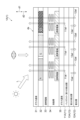
- FIG. 1 is a diagram illustrating an example of a configuration of a display device according to an embodiment of the present invention.
- 4 is a diagram illustrating a schematic configuration of a control unit that controls light emission from first and second light-emitting layers.
- FIG. 10 is a flowchart showing a light emission control process performed by a control unit.
- FIG. 13 is a diagram illustrating a configuration of another example of the display device according to the present embodiment.
- the display device of this embodiment is, for example, a self-luminous organic EL display or a liquid crystal display device.
- a self-luminous organic EL display displays images and the like by using elements such as OLEDs to emit light.
- a liquid crystal display device displays images and the like by using a backlight provided on the back side of the liquid crystal layer and made up of light-emitting elements to illuminate the liquid crystal layer.
- FIG. 1 is a diagram showing a schematic example of the configuration of a display device according to this embodiment.
- the display device 1 shown in FIG. 1 is a self-luminous display device, such as an organic EL display.
- the display device 1 includes a first light-emitting layer 11, a phosphorescent layer 12, and a second light-emitting layer 13.
- the display device 1 also includes a glass substrate 14, a transparent electrode 15, a TFT layer 16, a color filter 17, a TFT layer 18, and a glass substrate 19.
- the first light-emitting layer 11 is a layer that emits light (11l) in a first direction d1, which is the direction in which the display surface ds is facing.
- the first light-emitting layer 11 illustrated in FIG. 1 is a self-emitting element, for example, composed of an OLED.
- the first light-emitting layer 11 when a voltage is applied between the electrodes sandwiching the light-emitting layer, electrons and holes are injected from the cathode and anode, respectively, and electron-hole pairs are formed.
- the electrons and holes combine in the light-emitting layer to reach a high-energy state (excited state), and when they return from the high-energy state to the original stable energy state (ground state), the difference in energy is released as light, thereby realizing light emission 11l in the first light-emitting layer 11.
- the first light-emitting layer 11 is pixel-controlled by the TFT layer 16.
- the color of light emitted by each pixel in the first light-emitting layer 11 (e.g., R, G, or B) is determined by the molecular structure of the semiconductor used.
- the phosphorescent layer 12 is provided on the second direction d2 side of the first light-emitting layer 11, and is a layer that stores light received from the first direction d1 side (stores light energy).
- the second direction d2 is the opposite direction to the first direction d1.
- the phosphorescent layer 12 emits light (12l) in the first direction d1 based on the stored energy.
- the first direction d1 and the second direction d2 extend perpendicular to the display surface ds in FIG. 1 for convenience of illustration, but the first direction d1 as the direction of light emission 12l and the second direction d2, which is the opposite direction, are not limited to being perpendicular to the display surface ds.
- the luminous layer 12 stores external light L incident on the display surface ds.
- the luminous layer 12 also stores light emitted by the second light-emitting layer 13, which will be described later, through light emission 13l.
- the luminous layer 12 can be made of a material with known luminous properties, but as an example, it may be made of a long-lasting phosphor made of a strontium compound mixed with a trace amount of a rare earth element.
- the luminous layer 12 becomes excited by absorbing the energy of light, and emits light when it returns from the excited state to the ground state.
- the second light-emitting layer 13 is provided between the first light-emitting layer 11 and the phosphorescent layer 12, and emits light (13l) toward the phosphorescent layer 12.
- the second light-emitting layer 13 is composed of self-emitting elements like the first light-emitting layer 11, for example, light-emitting diodes. That is, in the second light-emitting layer 13, a voltage is applied between the electrodes sandwiching the light-emitting layer to cause the layer to enter an excited state, and the light emission 13l is realized by emitting the difference in energy as light when the layer returns from the excited state to the ground state.
- the second light-emitting layer 13 is pixel-controlled by the TFT layer 18 in the same way as the first light-emitting layer 11.
- the color of the light emitted by the second light-emitting layer 13 is not limited, but the second light-emitting layer 13 may be composed of, for example, a white light-emitting diode.
- the power consumption of the second light-emitting layer 13 is configured to be lower than the power consumption of the first light-emitting layer 11.
- the glass substrate 14 is a substrate made of transparent glass with a smooth surface, and forms the display surface ds of the display device 1.
- the transparent electrode 15 is an electrode made of a material that is transparent, such as glass, and conductive, such as a metal, and applies a voltage to the first light-emitting layer 11.
- the TFT layer 16 is a layer in which TFTs (Thin Film Transistors) are formed.
- the TFTs in the layer control the brightness of the light-emitting elements in the first light-emitting layer 11 for each pixel.
- the color filter 17 is a filter that gives color information such as RGB to the light emitted by the phosphorescent layer 12. This controls the color that appears on the display surface ds due to the light emission 12l from the phosphorescent layer 12 to be the same for each pixel as the color that appears on the display surface ds due to the light emission 11l of the first light-emitting layer 11.
- the TFT layer 18 is a layer in which TFTs are formed.
- the TFTs in the layer control the brightness of the light-emitting elements in the second light-emitting layer 13 for each pixel.
- the glass substrate 19 is a substrate made of transparent glass with a smooth surface, and forms the substrate of the display device 1.
- the display device 1 of this embodiment further includes an illuminance sensor SE and a control unit 20.
- FIG. 2 is a diagram showing a schematic configuration of the control unit that controls the light emission of the first and second light-emitting layers.
- the illuminance sensor SE acquires illuminance that represents the brightness of the light illuminating the display surface ds of the display device 1.
- the illuminance sensor SE may be a sensor that detects the illuminance of the environment surrounding the display device 1.
- the control unit 20 controls the light emission of the first light-emitting layer 11 and the second light-emitting layer 13 according to the illuminance state acquired by the illuminance sensor SE. Specifically, the control unit 20 controls the switch state ss according to the illuminance, thereby supplying power from the power source ES to the first light-emitting layer 11 and the second light-emitting layer 13 and controlling the light emission in the first light-emitting layer 11 and the second light-emitting layer 13.
- the control unit 20 may be realized by a dedicated circuit, or may be realized by a processor that executes a program to realize the functions of the control unit 20.
- FIG. 3 is a flowchart showing the light emission control process by the control unit 20.
- the control unit 20 controls the first light-emitting layer 11 to emit light and the second light-emitting layer 13 not to emit light
- the control unit 20 controls the first light-emitting layer 11 not to emit light and controls the phosphorescent layer 12 to emit light.
- step S1 the control unit 20 acquires the illuminance of the environment surrounding the display device 1, which is detected by the illuminance sensor SE.
- step S11 the control unit 20 determines whether or not it is the first case in which the illuminance is equal to or greater than the threshold value. If it is determined that it is the first case, the process proceeds to step S12. On the other hand, if it is not determined that it is the first case, that is, if it is determined that it is the second case in which the illuminance is less than the threshold value or equal to or less than the threshold value, the process proceeds to step S21.
- the threshold value for illuminance may be, for example, 200 lx, but the threshold value is not limited to this value.
- step S12 the control unit 20 controls the switch state ss to (2'b00).
- step S13 the control unit 20 controls the switch state ss to cause the first light-emitting layer 11 to emit light and to cause the second light-emitting layer 13 not to emit light.
- the phosphorescent layer 12 stores the external light L that illuminates the display surface ds and emits light in the first direction d1.
- the light emission 11l of the first light-emitting layer 11 displays images and the like on the display surface ds, while the light emission 12l from the phosphorescent layer 12 functions as a backlight to compensate for the amount of light. Therefore, in a high-illuminance environment, if there is insufficient light emission in the direction in which the display surface ds is facing, the visibility of the display decreases, but the light emission 12l from the phosphorescent layer 12 compensates for the amount of light, preventing the decrease in visibility.
- step S11 determines whether the switch state ss is (2'b00). If it is determined that the switch state ss is (2'b00), the process proceeds to step S22. On the other hand, if it is not determined that the switch state ss is (2'b00), the process proceeds to step S31.
- step S22 the control unit 20 controls the switch state ss to (2'b01).
- step S23 the control unit 20 controls the switch state ss so that the first light-emitting layer 11 does not emit light and the second light-emitting layer 13 emits light.
- the light-storing layer 12 stores low-illuminance external light L and stores light emitted 13l from the second light-emitting layer 13. The light-storing layer 12 then emits light in the first direction d1 based on the energy of the stored light.
- the display of images and the like on the display surface ds is realized by the light emission 12l of the phosphorescent layer 12 based on the storage of light emission 13l from the second light-emitting layer 13, which consumes less power than the first light-emitting layer 11, so it is possible to reduce power consumption by making the first light-emitting layer 11 non-emitting.
- step S24 the control unit 20 causes the second light-emitting layer 13 to emit light for a certain period of time, thereby causing the phosphorescent layer 12 to store light.
- This certain period of time may be set to any time, but is not limited to this period of time, and may be, for example, 30 seconds.
- step S25 when a certain time (given light emission time) has elapsed since the second light-emitting layer 13 was caused to emit light, the control unit 20 controls the switch state ss to (2'b1x), and in step S26, stops the light emission of the second light-emitting layer 13.
- the emission 13l of the second light-emitting layer 13 is stopped after a given emission time has elapsed, and the emission 12l of the phosphorescent layer 12 continues based on the energy already absorbed, making it possible to further reduce power consumption.
- step S31 the control unit 20 determines whether the amount of light emission 12l from the phosphorescent layer 12 is sufficient. Specifically, the control unit 20 may obtain information indicating whether the amount of light emission 12l from the phosphorescent layer 12 is sufficient based on an input operation on the display device 1 from a user viewing the display surface ds. The control unit 20 may also obtain information from an optical sensor (not shown) that is provided on the display device 1 and can detect the amount of light emission 12l from the phosphorescent layer 12, as information indicating whether the amount of light emission 12l from the phosphorescent layer 12 is sufficient.
- an optical sensor not shown
- step S32 If it is determined that the amount of light emission 12l from the phosphorescent layer 12 is sufficient, the process proceeds to step S32. On the other hand, if it is not determined that the amount of light emission 12l from the phosphorescent layer 12 is sufficient, the process proceeds to step S41.
- step S32 the control unit 20 controls the switch state ss to (2'b01).
- step S33 the control unit 20 controls the switch state ss so that the first light-emitting layer 11 does not emit light and the second light-emitting layer 13 does not emit light. In this way, when the amount of light emission 12l from the phosphorescent layer 12 is sufficient, the light emission 13l of the second light-emitting layer 13 is stopped and the light emission 12l in the phosphorescent layer 12 continues based on the energy that has already been absorbed, making it possible to further reduce power consumption.
- step S41 the control unit 20 controls the switch state ss to (2'b01).
- step S42 the control unit 20 controls the switch state ss to not cause the first light-emitting layer 11 to emit light, but causes the second light-emitting layer 13 to emit light.
- the phosphorescent layer 12 stores low-illuminance external light L and stores light emission 13l from the second light-emitting layer 13. The phosphorescent layer 12 then emits light in the first direction d1 based on the energy of the stored light.
- the display of images and the like on the display surface ds is realized by the light emission 12l of the phosphorescent layer 12 based on the storage of light emission 13l from the second light-emitting layer 13, which consumes less power than the first light-emitting layer 11, so it is possible to reduce power consumption by making the first light-emitting layer 11 non-emitting.
- step S43 the control unit 20 causes the second light-emitting layer 13 to emit light for a certain period of time, thereby storing light in the phosphorescent layer 12.
- This certain period of time may be set to any time, but is not limited to this period of time, and may be, for example, 30 seconds.
- step S44 when a certain time (given light emission time) has elapsed since the second light emitting layer 13 was made to emit light, the control unit 20 controls the switch state ss to (2'b1x), and in step S45, stops the light emission of the second light emitting layer 13. In this way, the light emission 13l of the second light emitting layer 13 is stopped after the given light emission time has elapsed, and the light emission 12l in the phosphorescent layer 12 continues based on the energy that has already been absorbed, making it possible to further reduce power consumption.
- FIG. 4 is a diagram showing a schematic configuration of another example of a display device according to this embodiment.
- the display device 1A(1) shown in FIG. 4 is a liquid crystal display device.
- a backlight composed of light-emitting elements provided on the rear surface of the liquid crystal layer illuminates the liquid crystal layer to display images, etc.
- the display device 1A includes a first light-emitting layer 11A (11), a phosphorescent layer 12A (12), and a second light-emitting layer 13A (13).
- the display device 1A also includes a glass substrate 31, a color filter 32, a transparent electrode 33, a liquid crystal layer 34, and a glass substrate 35.
- the first light-emitting layer 11A is a layer that emits light (11al) in a first direction d1, which is the direction in which the display surface ds is facing, and is a so-called backlight.
- the first light-emitting layer 11A is composed of light-emitting elements, such as light-emitting diodes.
- the color of light emitted by the first light-emitting layer 11A is not limited, and the first light-emitting layer 11A may be composed of, for example, a white light-emitting diode.
- the phosphorescent layer 12A is provided on the second direction d2 side of the first light-emitting layer 11A, and is a layer that stores light received from the first direction d1 side (stores light energy).
- the second direction d2 is the opposite direction to the first direction d1.
- the phosphorescent layer 12A emits light (12al) in the first direction d1 based on the stored energy.
- the first direction d1 and the second direction d2 extend perpendicular to the display surface ds in FIG. 1 for convenience of illustration, but the first direction d1 as the direction of light emission 12al and the second direction d2, which is the opposite direction, are not limited to being perpendicular to the display surface ds.
- the luminous layer 12A stores external light L incident on the display surface ds.
- the luminous layer 12 also stores light emitted by the second light-emitting layer 13A (described later) through light emission 13al.
- the luminous layer 12A like the luminous layer 12, can be made of a material with known luminous properties.
- the second light-emitting layer 13A is provided between the first light-emitting layer 11A and the phosphorescent layer 12A, and emits light (13al) toward the phosphorescent layer 12A.
- the second light-emitting layer 13A is composed of a self-emitting element like the first light-emitting layer 11A, for example, a light-emitting diode.
- the color of the light emitted by the second light-emitting layer 13A is not limited, and the second light-emitting layer 13A may be composed of, for example, a white light-emitting diode.
- the power consumption of the second light-emitting layer 13A is configured to be lower than the power consumption of the first light-emitting layer 11A.
- the glass substrate 31 is a substrate made of transparent glass with a smooth surface, and forms the display surface ds of the display device 1A.
- the color filter 32 is a filter that provides color information such as RGB to the light 11al emitted by the first light-emitting layer 11A that constitutes the backlight and passing through the liquid crystal layer 34, and to the light 12al emitted by the phosphorescent layer 12A and passing through the liquid crystal layer 34.
- the transparent electrode 33 is an electrode made of a material that is transparent, such as glass, and conducts electricity, such as a metal, and applies a voltage to the liquid crystal layer 34.
- the glass substrate 35 is a substrate made of transparent glass with a smooth surface, and forms the substrate of the display device 1A.
- the display device 1A includes an illuminance sensor SE and a control unit 20, similar to the display device 1 shown in FIG. 1.
- the control unit 20 of the display device 1A controls the emission of the first light-emitting layer 11A and the second light-emitting layer 13A according to the illuminance, similar to the control unit of the display device 1 described with reference to FIGS. 2 and 3, and controls the storage and emission of light in the phosphorescent layer 12A. In this way, even in the display device 1A constituted by a liquid crystal display device having a backlight, it is possible to improve visibility and reduce power consumption.
- the phosphorescent layer 12, 12A emits light in the first direction d1 based on the energy of the received light, thereby making it possible to supplement the brightness for display, thereby improving the visibility of the display when the illuminance of the external light L is high. Furthermore, when the illuminance is low, the display is realized by the emission of light from the phosphorescent layer 12, 12A based on the storage of light from the second light-emitting layer 13, 13A, so that, for example, it is possible to reduce the amount of light emitted by the first light-emitting layer 11, 11A or to make the first light-emitting layer 11, 11A non-emitting, thereby reducing power consumption.
- the display device may have the following configurations. The actions and effects of each configuration are described as follows.
- a display device includes a first light-emitting layer that emits light in a first direction, which is the direction in which the display surface is facing; a phosphorescent layer that is provided on a second direction side of the first light-emitting layer and stores light received from the first direction side, the second direction being the opposite direction to the first direction; and a second light-emitting layer that is provided between the first light-emitting layer and the phosphorescent layer and emits light toward the phosphorescent layer, the power consumption of the second light-emitting layer being lower than the power consumption of the first light-emitting layer, and the phosphorescent layer stores light from at least the second light-emitting layer and emits light in the first direction.
- the phosphorescent layer emits light in a first direction based on the energy of the received light, thereby making it possible to supplement the brightness for display, thereby improving the visibility of the display when the illuminance of external light is high. Furthermore, when the illuminance is low, the display is realized by the emission of light from the phosphorescent layer based on the storage of light from the second light-emitting layer, so it is possible, for example, to reduce the amount of light emitted by the first light-emitting layer or to make the first light-emitting layer non-emitting, thereby making it possible to reduce power consumption.
- the display device may further include an illuminance sensor that acquires an illuminance that indicates the brightness of the light illuminating the display surface of the display device, and a control unit that controls the first light-emitting layer to emit light and the second light-emitting layer not to emit light in a first case where the illuminance exceeds a given threshold value or is equal to or greater than the threshold value, and controls the first light-emitting layer not to emit light and the phosphorescent layer to emit light in a second case where the illuminance is equal to or less than the threshold value.
- an illuminance sensor that acquires an illuminance that indicates the brightness of the light illuminating the display surface of the display device
- a control unit that controls the first light-emitting layer to emit light and the second light-emitting layer not to emit light in a first case where the illuminance exceeds a given threshold value or is equal to or greater than the threshold value, and controls the first light-emitting layer not to emit light and
- the display in addition to the emission of light by the first light-emitting layer, the display is realized by the emission of light based on the storage of external light by the phosphorescent layer, so that good visibility of the display is maintained even in high illuminance. Also, in the second case, the display is realized by the emission of light from the phosphorescent layer without causing the first light-emitting layer to emit light, so that power consumption can be reduced.
- control unit may cause the second light-emitting layer to emit light, thereby causing the phosphorescent layer to store light and emit light.
- the light storage and emission of light in the phosphorescent layer is achieved by the emission of light from the second light-emitting layer, which consumes less power than the first light-emitting layer, making it possible to reduce the power consumption of the display device when displaying.
- control unit may cause the second light-emitting layer to emit light when the amount of light emitted from the phosphorescent layer is less than a predetermined level.
- the second light-emitting layer when the amount of light emitted from the phosphorescent layer is equal to or greater than a predetermined level, the second light-emitting layer is not caused to emit light, so that the phosphorescent layer continues to emit light based on the energy already absorbed. This makes it possible to reduce power consumption.
- control unit may stop the second light-emitting layer from emitting light when a given light-emitting time has elapsed since the second light-emitting layer was made to emit light.
- the emission of light from the second light-emitting layer is stopped after the emission time has elapsed, and the emission of light from the phosphorescent layer continues based on the energy already absorbed, thereby enabling further reduction in power consumption.
- the phosphorescent layer may store external light that illuminates the display surface and emit light in a first direction.
- the visibility of the display will decrease.
- the amount of light emitted from the phosphorescent layer compensates, preventing the decrease in visibility.
- the display device may be a self-luminous display device, and the first light-emitting layer may include elements that emit light in a plurality of different colors.
- the above aspect makes it possible to improve visibility and reduce power consumption in a self-luminous organic EL display composed of OLEDs, for example.
- the display device may be a liquid crystal display device
- the first light-emitting layer may be a backlight for the liquid crystal contained in the liquid crystal display device.
- the above aspect makes it possible to improve visibility and reduce power consumption in a liquid crystal display device with a backlight.
- determining may encompass a wide variety of actions.
- Determining and “determining” may include, for example, judging, calculating, computing, processing, deriving, investigating, looking up, search, inquiry (e.g., searching in a table, database, or other data structure), and considering ascertaining as “judging” or “determining.”
- determining and “determining” may include receiving (e.g., receiving information), transmitting (e.g., sending information), input, output, accessing (e.g., accessing data in memory), and considering ascertaining as “judging” or “determining.”
- judgment” and “decision” can include considering resolving, selecting, choosing, establishing, comparing, etc., to have been “judged” or “decided.” In other words, “judgment” and “decision” can include considering some action to have been “judged” or “decided.” Additionally, “judgment (decision)” can be interpreted as “assuming,” “ex
- the phrase “based on” does not mean “based only on,” unless expressly stated otherwise. In other words, the phrase “based on” means both “based only on” and “based at least on.”
- any reference to an element is not intended to generally limit the quantity or order of those elements. These designations may be used herein as a convenient method of distinguishing between two or more elements. Thus, a reference to a first and a second element does not imply that only two elements may be employed therein or that the first element must precede the second element in some way.
- the display device of the present disclosure may have the following configuration.
- a first light-emitting layer that emits light in a first direction, which is a direction in which the display surface is faced;
- a phosphorescent layer provided on a second direction side of the first light-emitting layer, the phosphorescent layer storing light received from the first direction side, the second direction being opposite to the first direction;
- a second light-emitting layer is provided between the first light-emitting layer and the phosphorescent layer, and emits light toward the phosphorescent layer.
- the power consumption of the second light-emitting layer is lower than the power consumption of the first light-emitting layer;
- the luminous layer stores light from at least the second light-emitting layer and emits light in the first direction.
- Display device [2] an illuminance sensor that acquires an illuminance representing the brightness of light illuminating a display surface of the display device;
- a control unit controls the first light-emitting layer to emit light and the second light-emitting layer not to emit light in a first case where the illuminance exceeds a given threshold value or is equal to or greater than the threshold value, and controls the first light-emitting layer not to emit light and the phosphorescent layer to emit light in a second case where the illuminance is equal to or less than the threshold value.
- the control unit causes the second light-emitting layer to emit light, thereby causing the light-storing layer to store light and emit light.
- the display device causes the second light-emitting layer to emit light when the amount of light emitted from the phosphorescent layer is less than a predetermined level.
- the display device according to [3].
- the control unit stops the emission of light from the second light-emitting layer when a given light-emitting time has elapsed since the second light-emitting layer was caused to emit light.
- the display device according to [3] or [4].
- a display device according to any one of [2] to [5].
- the display device is a self-luminous display device, the first light-emitting layer includes elements that emit light of a plurality of different emission colors; A display device according to any one of claims 1 to 6.
- the display device is a liquid crystal display device, the first light-emitting layer being a backlight for the liquid crystal contained in the liquid crystal display device; A display device according to any one of claims 1 to 6.
Landscapes
- Physics & Mathematics (AREA)
- Engineering & Computer Science (AREA)
- General Physics & Mathematics (AREA)
- Theoretical Computer Science (AREA)
- Nonlinear Science (AREA)
- Chemical & Material Sciences (AREA)
- Crystallography & Structural Chemistry (AREA)
- Computer Hardware Design (AREA)
- Mathematical Physics (AREA)
- Optics & Photonics (AREA)
- General Engineering & Computer Science (AREA)
- Electroluminescent Light Sources (AREA)
Priority Applications (1)
| Application Number | Priority Date | Filing Date | Title |
|---|---|---|---|
| JP2025556224A JPWO2025100069A1 (https=) | 2023-11-07 | 2024-09-04 |
Applications Claiming Priority (2)
| Application Number | Priority Date | Filing Date | Title |
|---|---|---|---|
| JP2023190164 | 2023-11-07 | ||
| JP2023-190164 | 2023-11-07 |
Publications (1)
| Publication Number | Publication Date |
|---|---|
| WO2025100069A1 true WO2025100069A1 (ja) | 2025-05-15 |
Family
ID=95695559
Family Applications (1)
| Application Number | Title | Priority Date | Filing Date |
|---|---|---|---|
| PCT/JP2024/031712 Pending WO2025100069A1 (ja) | 2023-11-07 | 2024-09-04 | 表示デバイス |
Country Status (2)
| Country | Link |
|---|---|
| JP (1) | JPWO2025100069A1 (https=) |
| WO (1) | WO2025100069A1 (https=) |
Citations (4)
| Publication number | Priority date | Publication date | Assignee | Title |
|---|---|---|---|---|
| JP2000171795A (ja) * | 1998-10-01 | 2000-06-23 | Miyuki Hayashi | 蓄光材式液晶表示装置 |
| JP2003084139A (ja) * | 2001-09-13 | 2003-03-19 | Toppan Printing Co Ltd | ホログラム反射板およびそれを搭載した反射型液晶表示装置 |
| JP2019053202A (ja) * | 2017-09-15 | 2019-04-04 | シャープ株式会社 | 表示装置 |
| JP2022188133A (ja) * | 2009-11-13 | 2022-12-20 | 株式会社半導体エネルギー研究所 | 表示装置 |
-
2024
- 2024-09-04 WO PCT/JP2024/031712 patent/WO2025100069A1/ja active Pending
- 2024-09-04 JP JP2025556224A patent/JPWO2025100069A1/ja active Pending
Patent Citations (4)
| Publication number | Priority date | Publication date | Assignee | Title |
|---|---|---|---|---|
| JP2000171795A (ja) * | 1998-10-01 | 2000-06-23 | Miyuki Hayashi | 蓄光材式液晶表示装置 |
| JP2003084139A (ja) * | 2001-09-13 | 2003-03-19 | Toppan Printing Co Ltd | ホログラム反射板およびそれを搭載した反射型液晶表示装置 |
| JP2022188133A (ja) * | 2009-11-13 | 2022-12-20 | 株式会社半導体エネルギー研究所 | 表示装置 |
| JP2019053202A (ja) * | 2017-09-15 | 2019-04-04 | シャープ株式会社 | 表示装置 |
Also Published As
| Publication number | Publication date |
|---|---|
| JPWO2025100069A1 (https=) | 2025-05-15 |
Similar Documents
| Publication | Publication Date | Title |
|---|---|---|
| US7176619B2 (en) | Self-luminescence image display unit | |
| JP4463392B2 (ja) | El表示装置の作製方法 | |
| US6674245B2 (en) | Active matrix organic electroluminescence display device and method of fabricating the same | |
| US10380946B2 (en) | OLED pixel circuitry, driving method thereof and display device | |
| KR20050075711A (ko) | 능동 매트릭스 디스플레이를 위한 픽셀 | |
| KR20120017661A (ko) | 유기 발광 표시 장치 | |
| GB2557135A (en) | Drive system and drive method for amoled display | |
| US20180240997A1 (en) | Double side oled display element and manufacture method thereof | |
| JP3872964B2 (ja) | ディスプレイ素子 | |
| US20090009443A1 (en) | Display Device | |
| KR102840689B1 (ko) | 전계발광소자 및 이를 포함하는 전계발광 표시장치 | |
| CN219372995U (zh) | 一种多层空穴注入层结构及显示装置 | |
| US20070057881A1 (en) | Transflective display having an OLED region and an LCD region | |
| WO2025100069A1 (ja) | 表示デバイス | |
| CN108922910A (zh) | Oled模组、显示面板及显示器 | |
| US8154507B2 (en) | Back light system and liquid crystal display device using the back light system | |
| US20070159087A1 (en) | Organic light-emitting device | |
| CN112909194B (zh) | 透明显示面板 | |
| KR100834341B1 (ko) | 능동행렬 유기전기발광소자 | |
| KR100782322B1 (ko) | 능동행렬 유기전기발광소자 및 그의 제조 방법 | |
| JP2003272835A (ja) | 有機発光素子及びその駆動方法 | |
| KR100623224B1 (ko) | 액정표시장치의 백라이트 및 그 제조 방법 | |
| KR100722115B1 (ko) | 유기 전계 발광 표시장치 | |
| KR101443372B1 (ko) | 유기발광표시장치 | |
| KR100729855B1 (ko) | 유기 전계 발광 소자 |
Legal Events
| Date | Code | Title | Description |
|---|---|---|---|
| 121 | Ep: the epo has been informed by wipo that ep was designated in this application |
Ref document number: 24888371 Country of ref document: EP Kind code of ref document: A1 |
|
| ENP | Entry into the national phase |
Ref document number: 2025556224 Country of ref document: JP Kind code of ref document: A |
|
| WWE | Wipo information: entry into national phase |
Ref document number: 2025556224 Country of ref document: JP |