WO2025089082A1 - 磁気抵抗素子、記憶装置および電子機器 - Google Patents
磁気抵抗素子、記憶装置および電子機器 Download PDFInfo
- Publication number
- WO2025089082A1 WO2025089082A1 PCT/JP2024/036216 JP2024036216W WO2025089082A1 WO 2025089082 A1 WO2025089082 A1 WO 2025089082A1 JP 2024036216 W JP2024036216 W JP 2024036216W WO 2025089082 A1 WO2025089082 A1 WO 2025089082A1
- Authority
- WO
- WIPO (PCT)
- Prior art keywords
- layer
- oxide layer
- thickness
- oxide
- memory
- Prior art date
- Legal status (The legal status is an assumption and is not a legal conclusion. Google has not performed a legal analysis and makes no representation as to the accuracy of the status listed.)
- Pending
Links
Images









Classifications
-
- H—ELECTRICITY
- H10—SEMICONDUCTOR DEVICES; ELECTRIC SOLID-STATE DEVICES NOT OTHERWISE PROVIDED FOR
- H10B—ELECTRONIC MEMORY DEVICES
- H10B61/00—Magnetic memory devices, e.g. magnetoresistive RAM [MRAM] devices
-
- H—ELECTRICITY
- H10—SEMICONDUCTOR DEVICES; ELECTRIC SOLID-STATE DEVICES NOT OTHERWISE PROVIDED FOR
- H10N—ELECTRIC SOLID-STATE DEVICES NOT OTHERWISE PROVIDED FOR
- H10N50/00—Galvanomagnetic devices
- H10N50/10—Magnetoresistive devices
-
- H—ELECTRICITY
- H10—SEMICONDUCTOR DEVICES; ELECTRIC SOLID-STATE DEVICES NOT OTHERWISE PROVIDED FOR
- H10N—ELECTRIC SOLID-STATE DEVICES NOT OTHERWISE PROVIDED FOR
- H10N50/00—Galvanomagnetic devices
- H10N50/20—Spin-polarised current-controlled devices
Definitions
- This disclosure relates to magnetoresistance elements, memory devices, and electronic devices.
- a Q-I (Quad-interface) type MTJ (Magnetic Tunnel Junction) element has been proposed as a magnetoresistance element with high retention characteristics ( ⁇ ) (see, for example, Patent Document 1).
- a Q-I type MTJ element is configured by stacking, for example, a reference layer, a barrier layer, a first magnetic layer, an intermediate layer, a second magnetic layer, and a cap layer in the order listed.
- the first magnetic layer, the intermediate layer, and the second magnetic layer function as a memory layer.
- a nonmagnetic layer for example, MgO
- MgO is used for the barrier layer, the intermediate layer, and the cap layer. Therefore, there are four interfaces where the first magnetic layer and the second magnetic layer contact the nonmagnetic layer.
- the interfacial magnetic anisotropy that appears at their interface is utilized.
- the first and second magnetic layers are magnetically coupled via an intermediate layer, and appear to function as a single magnetic layer.
- the total volume of the magnetic material increases in a Q-I MTJ element, and the retention characteristics are improved compared to a typical D-I (double-interface) MTJ element.
- the memory layer is a single magnetic layer, and there are two interfaces where the magnetic layer and nonmagnetic layer come into contact.
- the interfacial magnetic anisotropy increases, making it possible to further improve the retention characteristics.
- This disclosure provides a magnetoresistive element, a memory device, and an electronic device that can improve retention characteristics and suppress the decrease in the TMR ratio.
- a magnetoresistance element includes a reference layer, a barrier layer stacked on the reference layer, a memory layer stacked on the barrier layer, and a cap layer stacked on the memory layer, and the memory layer or the cap layer has a first oxide layer, a metal layer stacked on the first oxide layer, and a second oxide layer stacked on the metal layer.
- a storage device includes a magnetoresistance element, the magnetoresistance element including a reference layer, a barrier layer stacked on the reference layer, a memory layer stacked on the barrier layer, and a cap layer stacked on the memory layer, the memory layer or the cap layer including a first oxide layer, a metal layer stacked on the first oxide layer, and a second oxide layer stacked on the metal layer.
- An electronic device includes a memory device having a magnetoresistive element, the magnetoresistive element including a reference layer, a barrier layer stacked on the reference layer, a memory layer stacked on the barrier layer, and a cap layer stacked on the memory layer, the memory layer or the cap layer having a first oxide layer, a metal layer stacked on the first oxide layer, and a second oxide layer stacked on the metal layer.
- FIG. 1 is a diagram illustrating an example of the configuration of a storage device according to a first embodiment.
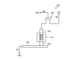
- 2 is a diagram showing a configuration example of a memory cell according to the first embodiment;
- 5 is a diagram showing another configuration example of the memory cell according to the first embodiment;
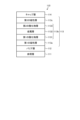
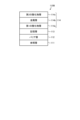
- FIG. 1 is a diagram showing a configuration example of a magnetoresistance element according to a first embodiment;
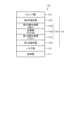
- 3A and 3B are diagrams illustrating a configuration example of a magnetoresistance element according to an example of the first embodiment.
- 5 is a diagram illustrating a configuration example of a magnetoresistance element according to a comparative example of the first embodiment.
- FIG. 1 is a diagram illustrating an example of the configuration of a storage device according to a first embodiment.
- 2 is a diagram showing a configuration example of a memory cell according to the first embodiment
- 5 is a diagram showing another configuration example of the memory cell according to the first embodiment
- FIG. 1 is a diagram showing a configuration example of a magnetores
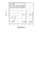
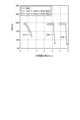
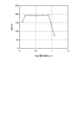
- 11 is a graph showing the relationship between the resistance RA and the thickness of the intermediate layer of magnetoresistive elements according to examples and comparative examples of the first embodiment.
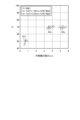
- 11 is a graph showing the relationship between the magnetoresistance ratio MR and the thickness of the intermediate layer of magnetoresistance elements according to examples and comparative examples of the first embodiment.
- 11 is a graph showing the relationship between the thermal stability index ⁇ and the thickness of the intermediate layer of magnetoresistance elements according to examples and comparative examples of the first embodiment.
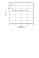
- 4 is a graph showing the relationship between the resistance RA and the thickness of a TaOx layer of a magnetoresistive element according to an example of the first embodiment.
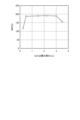
- FIG. 4 is a graph showing the relationship between the magnetoresistance ratio MR and the thickness of the TaOx layer of the magnetoresistance element according to the example of the first embodiment.
- 11 is a graph showing the relationship between the resistance RA and the thickness of the CoFeB layer of the magnetoresistive element according to the example of the first embodiment.
- 10 is a graph showing the relationship between the magnetoresistance ratio MR and the thickness of the CoFeB layer of the magnetoresistance element according to the example of the first embodiment.
- 11 is a graph showing the relationship between the resistance RA of the magnetoresistive element according to the example of the first embodiment and the thickness of the MgO layer.
- FIG. 10 is a graph showing the relationship between the magnetoresistance ratio MR of the magnetoresistance element according to the example of the first embodiment and the thickness of the MgO layer. 4 is a cross-sectional view showing a specific example of an insertion position of the magnetoresistive element according to the first embodiment into a chip.
- 11A and 11B are diagrams illustrating a configuration example of a magnetoresistance element according to a second embodiment.
- FIG. 1 is a diagram illustrating an application example of a storage device according to any one of the above-mentioned embodiments.
- FIG. 13 is a diagram illustrating a configuration example of an imaging device according to an application example.
- FIG. 13 is a diagram illustrating a configuration example of a distance measuring device according to an application example.
- each embodiment may contribute to solving a different purpose or problem, and may provide different effects. Note that the effects of each embodiment are merely examples and are not limiting, and other effects may also be provided.
- First embodiment 1-1 Configuration example of memory device 1-2.
- Second embodiment 2-1 Configuration example of magnetoresistance element 3. Function and effect according to each embodiment 4.
- FIG. 1 is a diagram showing an example of the configuration of a storage device 10 according to this embodiment.
- the memory device 10 includes a memory cell array 11.
- the memory device 10 is an example of a memory device that retains data based on the magnetization direction of a magnetic material.
- the memory cell array 11 includes a number of memory cells 100 arranged in a matrix. These memory cells 100 are connected to a bit line BL, a source line SL, and a word line WL.
- the word lines WL are each wired to extend in the row direction
- the bit lines BL and the source lines SL are each wired to extend in the column direction.
- the bit lines BL, source lines SL, and word lines WL each function as control lines.
- Each memory cell 100 has a magnetoresistance element (magnetoresistance effect element) 110 and a selection element 120.
- the magnetoresistance element 110 is, for example, an MTJ (Magnetic Tunnel Junction) element.
- the selection element 120 is connected to one end of the magnetoresistance element 110 and controls the application of voltage, current, etc. to the magnetoresistance element 110.
- various transistors can be used as this selection element 120.
- an STT (Spin Transfer Torque)-MRAM (Magnetoresistive Random Access Memory) cell or a VC-MRAM cell can be used as the memory cell 100.
- each memory cell 100 shares one source line SL for every two columns in the column direction.
- each memory cell 100 arranged in two columns in the column direction is connected to two bit lines BL and one source line SL (2BL/1SL).
- the memory device 10 includes peripheral circuits 20.
- the peripheral circuits 20 include an I/O (input/output circuit) 21, a control circuit 22, a voltage generation circuit 23, a write circuit 24, a read circuit 25, a bit line address decoder 26, a bit line control circuit 27, a word line address decoder 28, a word line control circuit 29, and a sense amplifier 30.
- the bit line control circuit 27 is connected to the bit line BL
- the word line control circuit 29 is connected to the word line WL
- the sense amplifier 30 is connected to the source line SL.
- the basic configuration of such a memory is publicly known, so the basic configuration will be briefly described.
- the I/O 21 enables the transfer of commands related to reading and writing data, the address of the memory cell 100 to be accessed, data, etc. between an external circuit (such as an arithmetic circuit) of the memory device 10 and the control circuit 22 of the memory device 10.
- an external circuit such as an arithmetic circuit
- the control circuit 22 performs control related to writing and reading data to and from the memory cell 100 in response to commands. For example, the control circuit 22 receives commands (such as commands for writing and reading) from an external circuit, and performs control related to writing and reading data based on the received commands.
- commands such as commands for writing and reading
- the voltage generation circuit 23 generates a voltage (e.g., a pulse voltage) used to write and read data to the memory cell 100, and supplies the generated voltage to the write circuit 24 and the read circuit 25. Note that the voltages required for circuit operation are provided separately.
- a voltage e.g., a pulse voltage
- the write circuit 24 controls the voltage and current (e.g., pulse voltage and pulse current) used to write data to the memory cell 100.
- the write circuit 24 functions as a write unit.
- the read circuit 25 controls the reading of data from the memory cell 100. Specifically, the read circuit 25 controls the voltage (e.g., pulse voltage) used to detect the resistance value of the magnetoresistance element 110. The read circuit 25 functions as a read unit.
- the voltage e.g., pulse voltage
- the bit line address decoder 26 obtains the address of the bit line BL corresponding to the address received by the I/O 21 described above.
- the bit line control circuit 27 selects and controls the bit line BL corresponding to the address of the bit line address decoder 26. For example, the writing of data to the memory cell 100 by the write circuit 24 and the reading of data from the memory cell 100 by the read circuit 25 are performed via the bit line control circuit 27 etc.
- the word line address decoder 28 obtains the address of the word line WL corresponding to the address received by the I/O 21 described above.
- the word line control circuit 29 selects and controls the word line WL that corresponds to the address of the word line address decoder 28.
- the sense amplifier 30 detects the data read from the memory cell 100 by the read circuit 25, specifically the resistance value of the magnetoresistance element 110.
- FIG. 2 and Fig. 3 are diagrams each showing a configuration example of the memory cell 100 according to this embodiment.
- the magnetoresistance element 110 and the selection element 120 of the memory cell 100 are connected in series, and the selection element 120 has a drain (drain terminal), a source (source terminal), and a gate (gate terminal).
- the contact layer 103 and the contact layer 104 correspond to, for example, an electrode layer or a connection layer.
- the magnetoresistance element 110 of the memory cell 100 is connected to the wiring 101 via the contact layer 103, for example, and to the selection element 120 via the contact layer 104.
- the drain of the selection element 120 is connected to the contact layer 104, and its source is connected to the source line SL.
- the gate of the selection element 120 is connected to the word line WL.
- the contact layer 103 is connected to the wiring 101 that constitutes the bit line BL.
- the magnetoresistance element 110 of the memory cell 100 is connected to the wiring 102 via the contact layer 104, for example, and to the selection element 120 via the contact layer 103.
- the drain of the selection element 120 is connected to the bit line BL, and its source is connected to the contact layer 103.
- the gate of the selection element 120 is connected to the word line WL.
- the contact layer 104 is connected to the wiring 102 that constitutes the source line SL.
- the bit line BL is connected to the bit line control circuit 27 (see FIG. 1).
- the word line WL is connected to the word line control circuit 29 (see FIG. 1).
- the source line SL is connected to the sense amplifier 30 (see FIG. 1).
- Fig. 4 is a diagram showing an example of the configuration of the magnetoresistance element 110 according to this embodiment.
- the magnetoresistance element 110 has a reference layer 111, a barrier layer 112, a memory layer 113, and a cap layer 114.
- the reference layer 111, the barrier layer 112, the memory layer 113, and the cap layer 114 are stacked in the order shown to form the magnetoresistance element 110.
- the reference layer 111 and the barrier layer 112 are adjacent, the barrier layer 112 and the memory layer 113 are adjacent, and the memory layer 113 and the cap layer 114 are adjacent. Adjacent layers share an interface, for example.
- the reference layer 111 is a layer that has magnetic anisotropy and whose magnetization direction is invariable. This reference layer 111 is also called, for example, a pinned layer or a magnetization pinned layer.
- the reference layer 111 may be made of, for example, CoFeB, a CoFeC alloy, a NiFeB alloy, a NiFeC alloy, or the like.
- the reference layer 111 may also be made of, for example, a laminated ferromagnetic pinned structure in which multiple ferromagnetic layers are laminated with a nonmagnetic layer interposed therebetween.
- the ferromagnetic layer that constitutes the reference layer 111 of this laminated ferromagnetic pinned structure may be made of, for example, Co, CoFe, CoFeB, Ni, Pd, or Pt.
- the nonmagnetic layer may be made of, for example, Ru, Re, Ir, or Os.
- the reference layer 111 may also be configured so that its magnetization direction is fixed by utilizing antiferromagnetic coupling between an antiferromagnetic layer and a ferromagnetic layer.
- the material of the antiferromagnetic layer may be, for example, a magnetic material such as an FeMn alloy, a PtMn alloy, a PtCrMn alloy, a NiMn alloy, an IrMn alloy, NiO, or Fe2O3.
- Nonmagnetic elements such as Ag, Cu, Au, Al, Si, Bi, Ta, B, C, O, N, Pd, Pt, Zr, Hf, Ir, W, Mo, or Nb may also be added to these magnetic materials.
- the barrier layer 112 is a layer disposed adjacent to the memory layer 113. This barrier layer 112 functions, for example, as a tunnel barrier layer.
- the barrier layer 112 may be composed of an oxide of at least one element selected from the group consisting of Mg, Al, Ti, Si, Zn, Zr, Hf, Ta, Bi, Cr, Ga, La, Gd, Sr, and Ba, or a nitride of at least one element selected from the group consisting of Mg, Al, Ti, Si, Zn, Zr, Hf, Ta, Bi, Cr, Ga, La, Gd, Sr, and Ba.
- the barrier layer 112 may also be composed of an insulator, dielectric, or semiconductor, such as MgF2, CaF, SrTiO2, AlLaO3, or AlNO, or may be composed of a structure in which these layers are stacked.
- the memory layer 113 is a layer that has magnetic anisotropy and a variable magnetization direction. This memory layer 113 is also called, for example, a free layer. A state in which the magnetization direction of the memory layer 113 is the same as that of the reference layer 111 is called a parallel state, and a state in which the magnetization direction of the memory layer 113 is different from that of the reference layer 111 is called an anti-parallel state.
- the magnetoresistance element 110 is in a low resistance state when in the parallel state, and in a high resistance state when in the anti-parallel state. As described above, the magnetization direction of the memory layer 113 can be changed by applying a voltage (current) to the magnetoresistance element 110.
- This memory layer 113 has a first magnetic layer 113a, an intermediate layer 113b, and a second magnetic layer 113c.
- the first magnetic layer 113a, the intermediate layer 113b, and the second magnetic layer 113c are stacked in the order shown to form the memory layer 113.
- the first magnetic layer 113a and the intermediate layer 113b are adjacent to each other, and the intermediate layer 113b and the second magnetic layer 113c are adjacent to each other.
- the first magnetic layer 113a is in contact with the non-magnetic layers of the barrier layer 112 and the intermediate layer 113b, and is arranged so as to be sandwiched between these non-magnetic layers.
- the second magnetic layer 113c is in contact with the non-magnetic layers of the intermediate layer 113b and the cap layer 114, and is arranged so as to be sandwiched between these non-magnetic layers. There are four interfaces where the first magnetic layer 113a and the second magnetic layer 113c contact the non-magnetic layers. Due to this arrangement, the magnetoresistance element 110 of this embodiment is called a Q-I type magnetoresistance element.
- the interfacial magnetic anisotropy that appears at the interface between the magnetic layer and the non-magnetic layer is utilized.
- the first magnetic layer 113a and the second magnetic layer 113c are magnetically coupled via the non-magnetic intermediate layer 113b, and appear to function as a single magnetic layer.
- the first magnetic layer 113a or the second magnetic layer 113c may be composed of, for example, CoFeB, CoFe, Fe, or FeB.
- the first magnetic layer 113a or the second magnetic layer 113c may also contain, for example, transition metals (Hf, Ta, W, Re, Ir, Pt, Au, Zr, Nb, Mo, Ru, Rh, Pd, Ag, Ti, V, Cr, Mn, Ni, or Cu).
- the first magnetic layer 113a or the second magnetic layer 113c may also contain, for example, nitrides or oxides.
- Ir or Os can be used as a material that induces a proximity magnetic moment in a magnetic material.
- the magnetic anisotropy effect can also be improved by adding a heavy metal to the first magnetic layer 113a or the second magnetic layer 113c.
- the intermediate layer 113b has a first oxide layer 1131, a metal layer 1132, and a second oxide layer 1133.
- the first oxide layer 1131, the metal layer 1132, and the second oxide layer 1133 are stacked in the order shown to form the intermediate layer 113b.
- the first oxide layer 1131 and the metal layer 1132 are adjacent to each other, and the metal layer 1132 and the second oxide layer 1133 are adjacent to each other.
- the first oxide layer 1131 or the second oxide layer 1133 may be composed of an oxide of one or more non-magnetic elements selected from, for example, Mg, Ta, Mo, W, Ti, Zr, Hf, Al, etc.
- the metal layer 1132 preferably contains, for example, B, and may be composed of a boride in which B is combined with a metal material selected from, for example, Co, Fe, Mo, Ti, W, etc.
- the cap layer 114 is a layer that protects the other layers, and is, for example, a layer that prevents diffusion of metals from wiring members, etc.
- This cap layer 114 may be composed of metals such as Cr, Ta, Ru, Au, Ag, Cu, Al, Ti, V, Mo, Zr, Hf, Re, W, Pt, Pd, Ir, and Rh.
- the cap layer 114 may also be composed of an alloy containing these, or a layer made of a transition metal element.
- the cap layer 114 may also be composed of a stack of these.
- the cap layer 114 may also be composed of a conductive nitride such as TiN.
- the magnetoresistance element 110 may have other layers in addition to the layers described above, such as a magnetic field generating layer that functions as a bias layer.
- the magnetic field generating layer generates a magnetic field that is applied in an in-plane direction (horizontal direction), for example.
- the in-plane direction is, for example, a direction perpendicular to the stacking direction (thickness direction) of the layers described above.
- a method other than the magnetic field generating layer may be used to generate the magnetic field. For example, a method of providing a magnet layer above or below the magnetoresistance element 110 or a method of arranging permanent magnets around the magnetoresistance element 110 may be used.
- the various layers described above may be formed by, for example, a sputtering method, an ion beam deposition method, a physical vapor deposition (PVD) method such as a vacuum deposition method, or a chemical vapor deposition (CVD) method such as an atomic layer deposition (ALD) method.
- the layers may be patterned by a reactive ion etching (RIE) method, an ion milling method, or the like.
- RIE reactive ion etching
- the various layers are preferably formed continuously in a vacuum device, and are preferably patterned after the formation of the various layers.
- the basic structure of the magnetoresistance element 110 is, as mentioned above, a sandwich structure in which a nonmagnetic layer, a barrier layer 112, is sandwiched between two magnetic layers, a reference layer 111 and a memory layer 113.
- This structure is called a magnetic tunnel junction (MTJ).
- MTJ magnetic tunnel junction
- the nonmagnetic layer is very thin, for example a few nm thick, a tunnel current flows when a voltage is applied to both ends of the magnetoresistance element 110.
- the magnitude of this tunnel current has the characteristic that it depends on the relative angle between the magnetization directions of the two magnetic layers. This is called the TMR (Tunnel Magneto Resistance) effect.
- the magnetization direction of one of the two magnetic layers (reference layer 111) is fixed, and the magnetization direction of the other magnetic layer (memory layer 113) is controlled by an external field.
- the magnetoresistance element 110 is in a low resistance state when the magnetization directions of the magnetic layers are the same in a parallel state, and in a high resistance state when the magnetization directions of the magnetic layers are different in an antiparallel state. Therefore, data (e.g., 0 or 1) is written to the memory cell 100 by switching the resistance state (resistance value) of the magnetoresistance element 110 to a low resistance state (low resistance value) or a high resistance state (high resistance value).
- an external field used to control the magnetization direction for example, a method using the STT effect or a method using the VCMA effect can be used. In addition, for reading data, for example, a method using the TMR effect can be used.
- the magnetization direction of the memory layer 113 is reversed by spin torque magnetization reversal.
- Writing is performed by applying a current to the memory layer 113 and causing spin torque magnetization reversal.
- the magnetization direction of the memory layer 113 changes and data is stored in the memory layer 113.
- the magnetization direction of the reference layer 111 is fixed and is used as the reference for the data (magnetization direction) of the memory layer 113.
- FIG. 5 is a diagram showing an example of the configuration of a magnetoresistance element 110 according to an example of this embodiment.
- FIG. 6 is a diagram showing an example of the configuration of a magnetoresistance element 110A as a comparative example according to this embodiment.
- the magnetoresistance element 110 has a reference layer 111, a barrier layer 112, a memory layer 113, and a cap layer 114, as described above.
- the memory layer 113 is composed of a first magnetic layer 113a, an intermediate layer 113b, and a second magnetic layer 113c.
- the intermediate layer 113b is composed of a first oxide layer 1131, a metal layer 1132, and a second oxide layer 1133.
- the first oxide layer 1131 is formed of TaOx (TaOx layer)
- the metal layer 1132 is formed of CoFeB (CoFeB layer)
- the second oxide layer 1133 is formed of MgO (MgO layer).
- This three-layer stacked configuration is sometimes described as TaOx/CoFeB/MgO, for example.
- the magnetoresistance element 110A of the comparative example has a reference layer 111, a barrier layer 112, a memory layer 113, and a cap layer 114, similar to the above-mentioned embodiment.
- the memory layer 113 is composed of a first magnetic layer 113a, an intermediate layer 113b, and a second magnetic layer 113c.
- the intermediate layer 113b is a single layer, and the single intermediate layer 113b is made of MgO (MgO layer).
- Fig. 7 is a graph showing the relationship between the resistance RA ( ⁇ m 2 ) and the thickness (nm) of the intermediate layer 113b of the magnetoresistance element 110 according to the embodiment and the magnetoresistance element 110A according to the comparative example.
- Fig. 8 is a graph showing the relationship between the magnetoresistance ratio MR (%) and the thickness (nm) of the intermediate layer 113b of the magnetoresistance element 110 according to the embodiment and the magnetoresistance element 110A according to the comparative example.
- Fig. 9 is a graph showing the relationship between the thermal stability index ⁇ and the thickness (nm) of the intermediate layer 113b of the magnetoresistance element 110 according to the embodiment and the magnetoresistance element 110A according to the comparative example.
- Graph G1a in FIG. 7, graph G1b in FIG. 8, and graph G1c in FIG. 9 are graphs relating to the magnetoresistance element 110A of the comparative example.
- Graph G2a in FIG. 7, graph G2b in FIG. 8, and graph G2c in FIG. 9 are graphs relating to the magnetoresistance element 110 of the embodiment in which the TaOx layer has a thickness of 1.05 nm.
- Graph G3a in FIG. 7, graph G3b in FIG. 8, and graph G3c in FIG. 9 are graphs relating to the magnetoresistance element 110 of the embodiment in which the TaOx layer has a thickness of 2.55 nm.
- the magnetoresistance ratio MR tends to decrease monotonically and rapidly when the thickness of the intermediate layer 113b exceeds 0.8 nm.
- the thermal stability index ⁇ increases rapidly with increasing thickness of the intermediate layer 113b, and decreases when the thickness exceeds 0.8 nm.
- the magnetoresistance ratio MR is the TMR ratio (tunnel magnetoresistance ratio).
- the TMR ratio represents the magnitude of the TMR effect (for example, the rate of change in the ease of current flow).
- the thickness range of the intermediate layer 113b exhibiting a high magnetoresistance ratio MR is limited to a very narrow thickness range of about 0.55 nm to 0.7 nm, as can be seen from the graph G1b of the comparative example shown in FIG. 8. It is difficult to control the thickness of the intermediate layer 113b within this very narrow thickness range, for example, by RF (radio frequency) sputtering using a PVD (physical vapor deposition) deposition device. In addition, as shown in the graph G1c of the comparative example shown in FIG. 9, there are situations in which the thermal stability index ⁇ is low. In addition, as described above, if the thickness of the intermediate layer 113b (the thickness of the MgO layer) is increased to increase the interface magnetic anisotropy, the magnetoresistance ratio MR decreases.
- the resistance RA does not increase as the thickness of the intermediate layer 113b increases, but remains almost constant, and increases sharply when the thickness exceeds 4.2 nm.
- the thickness range in which the resistance RA is almost constant is 3.4 nm or more and 4.2 nm or less.
- the resistance RA does not increase as the thickness of the intermediate layer 113b increases, but remains almost constant, and increases sharply when the thickness exceeds 5.7 nm.
- the thickness range in which the resistance RA is almost constant is 4.9 nm or more and 5.7 nm or less. In this way, the thickness range in which the resistance RA is almost constant can be secured to be 0.8 nm, i.e., about 1 nm.
- the thickness range of each of the graphs G2a and G3a of the examples is wider than the thickness range of the comparative example. Also, as shown in the graph G1a of the comparative example and the graphs G2a and G3a of the examples, even if the thickness of the intermediate layer 113b of the examples is several times thicker than the thickness of the intermediate layer 113b of the comparative example, the resistance RA is 10 ⁇ m2 or less .
- the magnetoresistance ratio MR does not increase with increasing thickness of the intermediate layer 113b, but remains almost constant, and decreases rapidly when the thickness exceeds 4.2 nm.
- the thickness range in which the magnetoresistance ratio MR is constant is 3.4 nm or more and 4.2 nm or less.
- the magnetoresistance ratio MR does not increase with increasing thickness of the intermediate layer 113b, but remains almost constant, and decreases rapidly when the thickness exceeds 5.7 nm.
- the thickness range in which the magnetoresistance ratio MR is almost constant is 4.9 nm or more and 5.7 nm or less. In this way, a thickness range of 0.8 nm, i.e., about 1 nm, can be secured as the thickness range in which the magnetoresistance ratio MR is almost constant.
- the magnetoresistance ratio MR is never approximately constant, but in graphs G2b and G3b of the examples, there is a thickness range where the magnetoresistance ratio MR is approximately constant. Also, as shown in graph G1b of the comparative example and graphs G2b and G3b of the examples, even if the thickness of the intermediate layer 113b of the example is made several times thicker than the thickness of the intermediate layer 113b of the comparative example, the magnetoresistance ratio MR is stable at around 190%.
- the thermal stability index ⁇ does not increase as the thickness of the intermediate layer 113b increases, but remains almost constant.
- the thermal stability index ⁇ is constant in the thickness range of 3.4 nm or more and 4.2 nm or less.
- the thermal stability index ⁇ does not increase as the thickness of the intermediate layer 113b increases, but remains almost constant.
- the thermal stability index ⁇ is almost constant in the thickness range of 4.9 nm or more and 5.7 nm or less. In this way, a thickness range of 0.8 nm, i.e., approximately 1 nm, can be secured as the thickness range in which the thermal stability index ⁇ is almost constant.
- the thermal stability index ⁇ is never approximately constant, but in graphs G2c and G3c of the examples, there is a thickness range where the thermal stability index ⁇ is approximately constant. Also, as shown in graph G1c of the comparative example and graphs G2c and G3c of the examples, even if the thickness of intermediate layer 113b of the example is made several times thicker than the thickness of intermediate layer 113b of the comparative example, the thermal stability index ⁇ is stable at around 70, which is greater than the thermal stability index ⁇ of the comparative example.
- the thickness of the intermediate layer 113b of the magnetoresistance element 110 of the embodiment is made thicker than that of the magnetoresistance element 110A of the comparative example, thereby increasing the interfacial magnetic anisotropy, improving the retention characteristics ( ⁇ ), and further suppressing the decrease in the magnetoresistance ratio MR.
- the magnetoresistance element 110 of the embodiment is superior to the magnetoresistance element 110A of the comparative example.
- the intermediate layer 113b consisting of the first oxide layer 1131, the metal layer 1132, and the second oxide layer 1133, it is possible to provide a magnetoresistance element 110 having a wide margin (film thickness margin) in the thickness of the intermediate layer 113b.
- the first oxide layer 1131 made of the above-mentioned non-magnetic layer elements, the metal layer 1132, and the second oxide layer 1133 made of the non-magnetic layer elements between the first magnetic layer 113a and the second magnetic layer 113c in the order described it is possible to suppress the increase in resistance caused by the intermediate layer 113b (parasitic resistance to the intermediate layer 113b) even with a relatively thick intermediate layer 113b, achieve a high TMR ratio (MR), and achieve high retention characteristics ( ⁇ ). This allows for a relatively wide margin in the thickness of the intermediate layer 113b, making it possible to design a stable mass production process.
- Thickness range of TaOx layer> The thickness range of the TaOx layer (first oxide layer 1131) according to the embodiment of the present invention will be described with reference to FIGS.
- Fig. 10 is a graph showing the relationship between the resistance RA ( ⁇ m 2 ) and the thickness (nm) of the TaOx layer of the magnetoresistance element 110 according to the example.
- Fig. 11 is a graph showing the relationship between the magnetoresistance ratio MR (%) and the thickness (nm) of the TaOx layer of the magnetoresistance element 110 according to the example.
- the behavior is explained by fixing the thickness of the CoFeB layer (metal layer 1132) to 2.2 nm and the thickness of the MgO layer (second oxide layer 1133) to 0.54 nm.
- the resistance RA increases, and as shown in Figure 11, the magnetoresistance ratio MR decreases. This is because, as the thickness of the TaOx layer becomes thinner in TaOx/CoFeB/MgO, the effect of the MgO layer becomes greater, and the parasitic resistance increases.
- the magnetoresistance ratio MR drops sharply. This is because when the thickness of the TaOx layer exceeds 2.6 nm, the total thickness of the intermediate layer 113b (the thickness of TaOx/CoFeB/MgO) becomes thick, and the magnetic coupling between the first magnetic layer 113a and the second magnetic layer 113c is broken, resulting in a drop in the magnetoresistance ratio MR and deterioration of the write characteristics.
- the thickness of the TaOx layer (first oxide layer 1131) be 1.0 nm or more and 2.6 nm or less. In this case, it is possible to suppress an increase in the resistance RA of the magnetoresistance element 110 and a decrease in the magnetoresistance ratio MR.
- Thickness range of CoFeB layer The thickness range of the CoFeB layer (metal layer 1132) according to the example of this embodiment will be described with reference to FIGS.
- Fig. 12 is a graph showing the relationship between the resistance RA ( ⁇ m 2 ) and the thickness (nm) of the CoFeB layer of the magnetoresistance element 110 according to the example.
- Fig. 13 is a graph showing the relationship between the magnetoresistance ratio MR (%) and the thickness (nm) of the CoFeB layer of the magnetoresistance element 110 according to the example.
- the behavior is explained by fixing the thickness of the TaOx layer (first oxide layer 1131) to 2.55 nm and the thickness of the MgO layer (second oxide layer 1133) to 0.54 nm.
- the magnetoresistance ratio MR decreases as the resistance RA increases, as shown in FIG. 13. This is because the insulating properties of the TaOx/CoFeB/MgO intermediate layer 113b gradually increase as the thickness of CoFeB decreases. Furthermore, when the thickness of the CoFeB layer exceeds 3.0 nm, the CoFeB layer exhibits in-plane magnetic anisotropy, weakening the magnetic coupling between the first magnetic layer 113a and the second magnetic layer 113c, and decreasing the magnetoresistance ratio MR.
- the thickness of the CoFeB layer (metal layer 1132) be 0.5 nm or more and 3.0 nm or less. In this case, it is possible to suppress an increase in the resistance RA of the magnetoresistance element 110 and a decrease in the magnetoresistance ratio MR.
- Thickness range of MgO layer> The thickness range of the MgO layer (second oxide layer 1133) according to the example of this embodiment will be described with reference to FIGS.
- Fig. 14 is a graph showing the relationship between the resistance RA ( ⁇ m 2 ) and the thickness (nm) of the MgO layer of the magnetoresistance element 110 according to the example.
- Fig. 15 is a graph showing the relationship between the magnetoresistance ratio MR (%) and the thickness (nm) of the MgO layer of the magnetoresistance element 110 according to the example.
- the behavior is explained by fixing the thickness of the TaOx layer (first oxide layer 1131) to 2.55 nm and the thickness of the CoFeB layer (metal layer 1132) to 2.2 nm.
- the resistance RA increases, and as the resistance RA increases, the magnetoresistance ratio MR decreases, as shown in FIG. 15. Furthermore, when the thickness of the MgO layer is thinner than 0.18 nm, the perpendicular magnetic anisotropy of the second magnetic layer 113c weakens, and the magnetoresistance ratio MR decreases.
- the thickness of the MgO layer (second oxide layer 1133) be 0.18 nm or more and 0.9 nm or less. In this case, it is possible to suppress an increase in the resistance RA of the magnetoresistance element 110 and a decrease in the magnetoresistance ratio MR.
- the metal layer 1132 may be configured to preferably contain B and at least one element selected from Co and Fe.
- the metal layer 1132 may contain Mo, Ti, W, etc. As an example of such a material, the following materials can be selected.
- CoB CoB, CoMoB, CoTiB, CoWB
- FeB FeMoB, FeTiB, FeWB 3) CoFeMoB, CoFeTiB, CoFeWB
- Fig. 16 is a cross-sectional view showing a specific example of the insertion position of the magnetoresistance element 110 according to this embodiment into the chip 500.
- the chip 500 has a semiconductor layer 510 and multiple wiring layers 520, 530, 540, and 550.
- the semiconductor layer 510 and the wiring layers 520, 530, 540, and 550 form part of the chip 500.
- the chip 500 includes a logic section 500a and a memory section 500b.
- the memory section 500b functions as, for example, an MRAM section.
- the logic section 500a and the memory section 500b are mounted together on, for example, one chip 500.
- the semiconductor layer 510 is, for example, a silicon substrate.
- the wiring layer 520 is, for example, a dielectric layer including various elements 521 such as transistors and multiple wirings.
- the wiring layer 530 is, for example, a dielectric layer including multiple wirings such as vias 531 and multiple magnetoresistance elements 110. In other words, each magnetoresistance element 110 is provided in the wiring layer 530, and this wiring layer 530 functions as an MRAM layer.
- the wiring layer 540 is, for example, a dielectric layer including multiple wirings such as vias 541.
- the wiring layer 550 is, for example, a dielectric layer including multiple wirings such as vias 551 and a metal layer 552. Note that each magnetoresistance element 110 may be provided in a layer other than the wiring layer 530, and the stacked structure of FIG. 16 is merely an example.
- Second embodiment 2-1 Configuration examples of magnetoresistance elements
- a configuration example of the magnetoresistance element 110B according to this embodiment will be described with reference to Fig. 17.
- Fig. 17 is a diagram showing a configuration example of the magnetoresistance element 110B according to this embodiment. This embodiment is basically the same as the first embodiment, but differences therebetween will be described.
- the cap layer 114 has a first oxide layer 114a, a metal layer 114b, and a second oxide layer 114c.
- the first oxide layer 114a corresponds to the first oxide layer 1131 according to the first embodiment
- the metal layer 114b corresponds to the metal layer 1132 according to the first embodiment
- the second oxide layer 114c corresponds to the second oxide layer 1133 according to the first embodiment.
- the memory layer 113 may be composed of a single layer or multiple layers, and may be composed in the same manner as the first magnetic layer 113a or the second magnetic layer 113c, for example.
- the cap layer 114 by forming the cap layer 114 by stacking the first oxide layer 114a, the metal layer 114b, and the second oxide layer 114c in the order listed, it is possible to suppress the increase in resistance caused by the cap layer 114 (parasitic resistance to the cap layer 114) even if the thickness of the cap layer 114 is made relatively thick, and it is possible to obtain a magnetoresistance element 110B with high magnetic anisotropy, thereby realizing a high TMR ratio (MR) and high retention characteristics ( ⁇ ).
- MR TMR ratio
- ⁇ retention characteristics
- the materials for each layer can be, for example, the same as those in the first embodiment.
- the same effect as in the first embodiment can be obtained. That is, by forming the cap layer 114 with the first oxide layer 114a, the metal layer 114b, and the second oxide layer 114c, it is possible to improve the retention characteristics and suppress the decrease in the TMR ratio.
- the magnetoresistance element 110 includes a reference layer 111, a barrier layer 112 laminated on the reference layer 111, a memory layer 113 laminated on the barrier layer 112, and a cap layer 114 laminated on the memory layer 113, and the memory layer 113 or the cap layer 114 has a first oxide layer 1131 (114a), a metal layer 1132 (114b) laminated on the first oxide layer 1131 (114a), and a second oxide layer 1133 (114c) laminated on the metal layer 1132 (114b) (see FIG. 4 and FIG. 17).
- the thickness of the memory layer 113 or the cap layer 114 is increased, it is possible to suppress the increase in resistance caused by the memory layer 113 or the cap layer 114, and obtain a high retention characteristic ( ⁇ ) and a high TMR ratio (MR). Therefore, it is possible to improve the retention characteristics and suppress the decrease in the TMR ratio.
- the memory layer 113 may have a first magnetic layer 113a laminated on the barrier layer 112, an intermediate layer 113b laminated on the first magnetic layer 113a, and a second magnetic layer 113c laminated on the intermediate layer 113b, and the intermediate layer 113b may have a first oxide layer 1131, a metal layer 1132, and a second oxide layer 1133 (see FIG. 4).
- This makes it possible to suppress an increase in resistance caused by the memory layer 113 even if the thickness of the memory layer 113 is increased, and to obtain high retention characteristics ( ⁇ ) and a high TMR ratio (MR), thereby realizing an improvement in retention characteristics and suppression of a decrease in the TMR ratio.
- the metal layer 1132 (114b) may be adjacent to the first oxide layer 1131 (114a), and the second oxide layer 1133 (114c) may be adjacent to the metal layer 1132 (114b) (see Figures 4 and 17). This ensures that the retention characteristics are improved and the decrease in the TMR ratio is suppressed.
- the first oxide layer 1131 (114a) and the second oxide layer 1133 (114c) may be formed of an oxide containing at least one non-magnetic element selected from the group consisting of Mg, Ta, Mo, W, Ti, Zr, Hf, and Al (see FIG. 4, etc.). This ensures that the retention characteristics are improved and the decrease in the TMR ratio is suppressed.
- the metal layer 1132 (114b) may also contain at least one of the elements Co and Fe (see FIG. 4, etc.). This can reliably improve retention characteristics and prevent a decrease in the TMR ratio.
- the metal layer 1132 (114b) may further contain B (see FIG. 4, etc.). This can reliably improve retention characteristics and suppress the decrease in the TMR ratio.
- the metal layer 1132 (114b) may further contain at least one of the elements Mo, Ti, and W (see FIG. 4, etc.). This can reliably improve retention characteristics and prevent a decrease in the TMR ratio.
- the first oxide layer 1131 (114a) and the second oxide layer 1133 (114c) may be formed from oxides containing different non-magnetic elements (see FIG. 5, etc.). This can reliably improve retention characteristics and prevent a decrease in the TMR ratio.
- the first oxide layer 1131 (114a) may be made of TaOx, and the second oxide layer 1133 (114c) may be made of MgO (see FIG. 5, etc.). This ensures that the retention characteristics are improved and the decrease in the TMR ratio is suppressed.
- the metal layer 1132 (114b) may also be made of CoFeB (see FIG. 5, etc.). This ensures that the retention characteristics are improved and the decrease in the TMR ratio is suppressed.
- the thickness of the first oxide layer 1131 (114a) may be 1.0 nm or more and 2.6 nm or less (see Figures 10 and 11). This makes it possible to suppress an increase in the resistance RA and a decrease in the magnetoresistance ratio MR of the magnetoresistance element 110 (110B).
- the first oxide layer 1131 (114a) may have a thickness of 1.0 nm or more and 2.6 nm or less and may be made of TaOx (see Figures 10 and 11). This can reliably suppress an increase in the resistance RA and a decrease in the magnetoresistance ratio MR of the magnetoresistance element 110 (110B).
- the thickness of the metal layer 1132 (114b) may be 0.5 nm or more and 3.0 nm or less (see Figures 12 and 13). This makes it possible to suppress an increase in the resistance RA and a decrease in the magnetoresistance ratio MR of the magnetoresistance element 110 (110B).
- the metal layer 1132 (114b) may have a thickness of 0.5 nm or more and 3.0 nm or less and may be made of CoFeB (see Figures 12 and 13). This can reliably suppress an increase in the resistance RA and a decrease in the magnetoresistance ratio MR of the magnetoresistance element 110 (110B).
- the thickness of the second oxide layer 1133 (114c) may be 0.18 nm or more and 0.9 nm or less (see Figures 14 and 15). This makes it possible to suppress an increase in the resistance RA and a decrease in the magnetoresistance ratio MR of the magnetoresistance element 110 (110B).
- the second oxide layer 1133 (114c) may have a thickness of 0.18 nm or more and 0.9 nm or less and may be made of MgO (see Figures 14 and 15). This can reliably suppress an increase in the resistance RA and a decrease in the magnetoresistance ratio MR of the magnetoresistance element 110 (110B).
- the thickness of the first oxide layer 1131 (114a) may be greater than the thickness of the second oxide layer 1133 (114c) (see Figures 10, 11, 14 and 15). This makes it possible to suppress an increase in the resistance RA and a decrease in the magnetoresistance ratio MR of the magnetoresistance element 110 (110B).
- the first oxide layer 1131 (114a) may be thicker than the second oxide layer 1133 (114c) and made of TaOx, and the second oxide layer 1133 (114c) may be made of MgO (see Figures 10, 11, 14 and 15). This can reliably prevent an increase in the resistance RA and a decrease in the magnetoresistance ratio MR of the magnetoresistance element 110 (110B).
- each configuration and each process in the above-described embodiment does not necessarily have to be physically configured as illustrated.
- the specific form of distribution and integration of each configuration and each process is not limited to that illustrated, and all or part of them may be functionally or physically distributed or integrated in any unit depending on various loads, usage conditions, etc.
- Fig. 18 is a diagram showing an application example of the storage device 10 according to any of the above-mentioned embodiments.
- the storage device 10 may be applied to various cases where light such as visible light, infrared light, ultraviolet light, and X-rays is sensed, for example, as described below.
- the storage device 10 may be applied to various devices (electronic devices) such as those described below, or electronic devices mounted on various devices.
- the storage device 10 is used in, for example, “devices for capturing images for viewing, such as digital cameras and mobile devices with camera functions," “devices for traffic use, such as in-vehicle sensors for capturing images of the front, rear, surroundings, and interior of a vehicle for safe driving such as automatic stopping and for recognizing the driver's state, surveillance cameras for monitoring moving vehicles and roads, and distance measuring sensors for measuring distances between vehicles," “devices for home appliances such as TVs, refrigerators, and air conditioners for capturing images of user gestures and operating the device according to the gestures,” “devices for medical and healthcare use, such as endoscopes and devices for capturing images of blood vessels by receiving infrared light," “devices for security use, such as surveillance cameras for crime prevention and cameras for person authentication,” “devices for beauty use, such as skin measuring devices for capturing images of the skin and microscopes for capturing images of the scalp,” “devices for sports use, such
- the technology disclosed herein can be applied to a variety of products.
- the technology disclosed herein may be realized as electronic devices mounted on any type of moving object, such as an automobile, electric vehicle, hybrid electric vehicle, motorcycle, bicycle, personal mobility, airplane, drone, ship, robot, construction machinery, agricultural machinery (tractor), etc.
- the technology disclosed herein may be realized as electronic devices mounted on an endoscopic surgery system, a microsurgery system, etc.
- Imaging device 300 An imaging device 300 according to an application example will be described with reference to Fig. 19.
- Fig. 19 is a diagram showing a configuration example of the imaging device 300 according to the application example.
- the imaging device 300 is an example of an electronic device to which the storage device 10 according to any of the above-mentioned embodiments is applied.
- Examples of the imaging device 300 include electronic devices such as digital still cameras, video cameras, and smartphones and mobile phones having imaging functions.
- the imaging device 300 includes an optical system 301, a shutter device 302, an imaging element (solid-state imaging device) 303, a control circuit (drive circuit) 304, a signal processing circuit 305, a monitor 306, and a memory 307.
- This imaging device 300 is capable of capturing still images and moving images.
- the optical system 301 has one or more lenses. This optical system 301 guides light from the subject (incident light) to the image sensor 303, forming an image on the light receiving surface of the image sensor 303.
- the shutter device 302 is disposed between the optical system 301 and the image sensor 303. This shutter device 302 controls the light irradiation period and the light blocking period for the image sensor 303 according to the control of the control circuit 304.
- the image sensor 303 accumulates signal charge for a certain period of time in response to light that is focused on the light receiving surface via the optical system 301 and the shutter device 302.
- the signal charge accumulated in the image sensor 303 is transferred in accordance with a drive signal (timing signal) supplied from the control circuit 304.
- a drive signal timing signal supplied from the control circuit 304.
- the image sensor 303 for example, a solid-state image sensor such as an image sensor is used.
- the control circuit 304 drives the image sensor 303 and the shutter device 302 by outputting a drive signal that controls the transfer operation of the image sensor 303 and the shutter operation of the shutter device 302.
- the signal processing circuit 305 performs various signal processing on the signal charges output from the image sensor 303.
- the image (image data) obtained by the signal processing performed by the signal processing circuit 305 is supplied to the monitor 306 and also to the memory 307.
- the monitor 306 displays a moving image or a still image captured by the image sensor 303 based on the image data supplied from the signal processing circuit 305.
- a panel-type display device such as a liquid crystal panel or an organic EL (Electro Luminescence) panel is used.
- the memory 307 stores image data supplied from the signal processing circuit 305, i.e., image data of moving images or still images captured by the image sensor 303.
- image data supplied from the signal processing circuit 305 i.e., image data of moving images or still images captured by the image sensor 303.
- a storage device 10 according to any of the above-mentioned embodiments is used.
- FIG. 20 is a diagram showing a configuration example of a distance measuring device 400 according to an application example.
- This distance measuring device 400 is an example of an electronic device to which the storage device 10 according to any one of the above-mentioned embodiments is applied.
- the distance measuring device (distance image sensor) 400 includes a light source unit 401, an optical system 402, an image sensor (solid-state image sensor) 403, a control circuit (drive circuit) 404, a signal processing circuit 405, a monitor 406, and a memory 407.
- This distance measuring device 400 projects light from the light source unit 401 toward the subject and receives light (modulated light or pulsed light) reflected from the surface of the subject, thereby obtaining a distance image according to the distance to the subject.
- the light source unit 401 projects light toward the subject.
- the light source unit 401 may be a vertical cavity surface emitting laser (VCSEL) array that emits laser light as a surface light source, or a laser diode array in which laser diodes are arranged in a line.
- the laser diode array is supported by a specified drive unit (not shown) and is scanned in a direction perpendicular to the direction in which the laser diodes are arranged.
- the optical system 402 has one or more lenses. This optical system 402 guides light from the subject (incident light) to the image sensor 403, forming an image on the light receiving surface (sensor section) of the image sensor 403.
- the imaging element 403 accumulates signal charges in response to light that is imaged on the light receiving surface via the optical system 402. A distance signal indicating the distance determined from the light receiving signal (APD OUT) output from this imaging element 403 is supplied to a signal processing circuit 405.
- a solid-state imaging device such as an image sensor is used.
- the control circuit 404 outputs a drive signal (control signal) that controls the operation of the light source unit 401, the image sensor 403, etc., and drives the light source unit 401, the image sensor 403, etc.
- the signal processing circuit 405 performs various types of signal processing on the distance signal supplied from the image sensor 403. For example, the signal processing circuit 405 performs image processing (e.g., histogram processing and peak detection processing) to construct a distance image based on the distance signal.
- image processing e.g., histogram processing and peak detection processing
- the image (image data) obtained by the signal processing performed by the signal processing circuit 405 is supplied to the monitor 406 and also to the memory 407.
- the monitor 406 displays the distance image captured by the image sensor 403 based on the image data supplied from the signal processing circuit 405.
- a panel-type display device such as a liquid crystal panel or an organic EL panel is used.
- the memory 407 stores image data supplied from the signal processing circuit 405, i.e., image data of the distance image captured by the image sensor 403.
- the memory 407 for example, a storage device 10 according to any of the above-mentioned embodiments is used.
- the distance measuring device 400 configured in this way, by applying the storage device 10 according to any of the above-mentioned embodiments as the memory 407, it is possible to improve the retention characteristics and suppress the decrease in the TMR ratio.
- the storage device 10 can be implemented in various electronic devices.
- the storage device 10 according to any of the above-mentioned embodiments may be mounted on various electronic devices such as an HDD (hard disk drive), a notebook PC (personal computer), a mobile device (e.g., a smartphone or tablet PC), a PDA (personal digital assistant), a wearable device, a game device, or a music device, in addition to the imaging device 300 or the distance measuring device 400.
- the storage device 10 may be used as various types of memory such as storage.
- the present technology can also be configured as follows. (1) A reference layer; a barrier layer laminated on the reference layer; a memory layer laminated on the barrier layer; a cap layer laminated on the memory layer; Equipped with The storage layer or the cap layer is a first oxide layer; a metal layer laminated to the first oxide layer; a second oxide layer disposed on the metal layer; having Magnetoresistance element. (2) The memory layer is a first magnetic layer laminated on the barrier layer; an intermediate layer laminated on the first magnetic layer; a second magnetic layer laminated on the intermediate layer; having The intermediate layer is the first oxide layer; The metal layer; the second oxide layer; having A magnetoresistance element according to (1).
- the metal layer is adjacent to the first oxide layer; the second oxide layer is adjacent to the metal layer; A magnetoresistance element according to (1) or (2).
- the first oxide layer and the second oxide layer are formed of an oxide containing at least one nonmagnetic element selected from the group consisting of Mg, Ta, Mo, W, Ti, Zr, Hf, and Al; A magnetoresistance element according to any one of (1) to (3).
- the metal layer contains at least one element selected from the group consisting of Co and Fe.
- the metal layer further contains B.
- the metal layer further contains at least one element selected from the group consisting of Mo, Ti, and W.
- the first oxide layer and the second oxide layer are formed of oxides containing different nonmagnetic elements; A magnetoresistance element according to any one of (1) to (7).
- the first oxide layer is formed of TaOx,
- the second oxide layer is formed of MgO.
- the metal layer is formed of CoFeB.
- the thickness of the first oxide layer is 1.0 nm or more and 2.6 nm or less.
- the first oxide layer is formed of TaOx.
- the thickness of the metal layer is 0.5 nm or more and 3.0 nm or less.
- the metal layer is formed of CoFeB.
- the thickness of the second oxide layer is 0.18 nm or more and 0.9 nm or less.
- the second oxide layer is formed of MgO.
- the thickness of the first oxide layer is greater than the thickness of the second oxide layer.
- the first oxide layer is formed of TaOx, The second oxide layer is formed of MgO.
- a magnetoresistance element according to (17).
- the magnetoresistive element is A reference layer; a barrier layer laminated on the reference layer; a memory layer laminated on the barrier layer; a cap layer laminated on the memory layer; Equipped with The storage layer or the cap layer is a first oxide layer; a metal layer laminated to the first oxide layer; a second oxide layer disposed on the metal layer; having Storage device.
- a storage device having a magnetoresistive element The magnetoresistive element is A reference layer; a barrier layer laminated on the reference layer; a memory layer laminated on the barrier layer; a cap layer laminated on the memory layer; Equipped with The storage layer or the cap layer is a first oxide layer; a metal layer laminated to the first oxide layer; a second oxide layer disposed on the metal layer; having Electronic devices.
- An electronic device comprising the storage device according to (21).
- Storage device 11 Memory cell array 20 Peripheral circuit 21 I/O 22 Control circuit 23 Voltage generation circuit 24 Write circuit 25 Read circuit 26 Bit line address decoder 27 Bit line control circuit 28 Word line address decoder 29 Word line control circuit 30 Sense amplifier 100 Memory cell 101 Wiring 102 Wiring 103 Contact layer 104 Contact layer 110 Magnetoresistance element 111 Reference layer 112 Barrier layer 113 Memory layer 113a First magnetic layer 113b Intermediate layer 113c Second magnetic layer 1131 First oxide layer 1132 Metal layer 1133 Second oxide layer 114 Cap layer 114a First oxide layer 114b Metal layer 114c Second oxide layer 120 Selection element 300 Imaging device 307 Memory 400 Distance measuring device 407 Memory SL Source line WL Word line
Landscapes
- Hall/Mr Elements (AREA)
Abstract
本開示の一形態に係る磁気抵抗素子は、参照層と、前記参照層に積層されたバリア層と、前記バリア層に積層された記憶層と、前記記憶層に積層されたキャップ層と、を備え、前記記憶層または前記キャップ層は、第1の酸化物層と、前記第1の酸化物層に積層された金属層と、前記金属層に積層された第2の酸化物層と、を有する。
Description
本開示は、磁気抵抗素子、記憶装置および電子機器に関する。
高い保持特性(Δ)を有する磁気抵抗素子として、Q-I(Quad-interface)型のMTJ(磁気トンネル接合)素子が提案されている(例えば、特許文献1参照)。Q-I型のMTJ素子は、例えば、参照層、バリア層、第1の磁性層、中間層、第2の磁性層およびキャップ層がその記載順で積層されて構成されている。第1の磁性層、中間層および第2の磁性層は、記憶層として機能する。バリア層、中間層およびキャップ層には、非磁性層(例えば、MgO)が用いられる。このため、第1の磁性層および第2の磁性層と非磁性層とが接する界面は四カ所となる。
前述の第1の磁性層および第2の磁性層が垂直磁化層となるためには、それらの界面で発現する界面磁気異方性が利用されている。第1の磁性層および第2の磁性層は、中間層を介して磁気的に結合しており、見かけ上一つの磁性層として機能する。このため、Q-I型のMTJ素子ではトータルの磁性体の体積が増えるので、保持特性は一般的なD-I(Double-interface)型のMTJ素子に比べて向上する。なお、D-I型のMTJ素子では、記憶層は一層の磁性層であり、磁性層と非磁性層とが接する界面は二カ所となる。また、Q-I型のMTJ素子では中間層の膜厚を厚くすることで、界面磁気異方性がより高くなるため、保持特性をさらに高めることが可能となる。
しかしながら、Q-I型などの磁気抵抗素子において、保持特性の向上のために中間層(例えば、MgO)の厚さを厚くすると、中間層起因(例えば、MgO起因)の寄生抵抗が発現し、TMR比(トンネル磁気抵抗比)が低下してしまう。
そこで、本開示では、保持特性の向上およびTMR比の低下の抑制を実現することが可能な磁気抵抗素子、記憶装置および電子機器を提供する。
本開示の一形態に係る磁気抵抗素子は、参照層と、前記参照層に積層されたバリア層と、前記バリア層に積層された記憶層と、前記記憶層に積層されたキャップ層と、を備え、前記記憶層または前記キャップ層は、第1の酸化物層と、前記第1の酸化物層に積層された金属層と、前記金属層に積層された第2の酸化物層と、を有する。
本開示の一形態に係る記憶装置は、磁気抵抗素子を備え、前記磁気抵抗素子は、参照層と、前記参照層に積層されたバリア層と、前記バリア層に積層された記憶層と、前記記憶層に積層されたキャップ層と、を備え、前記記憶層または前記キャップ層は、第1の酸化物層と、前記第1の酸化物層に積層された金属層と、前記金属層に積層された第2の酸化物層と、を有する。
本開示の一形態に係る電子機器は、磁気抵抗素子を有する記憶装置を備え、前記磁気抵抗素子は、参照層と、前記参照層に積層されたバリア層と、前記バリア層に積層された記憶層と、前記記憶層に積層されたキャップ層と、を備え、前記記憶層または前記キャップ層は、第1の酸化物層と、前記第1の酸化物層に積層された金属層と、前記金属層に積層された第2の酸化物層と、を有する。
以下に本開示の実施形態について図面に基づいて詳細に説明する。実施形態は、実施例や変形例なども含む。なお、本開示の実施形態により本開示に係る素子や装置、機器、方法などは限定されるものではない。また、以下の実施形態において、基本的に同一の部位には同一の符号を付することにより重複する説明を省略する。
以下の1または複数の実施形態は、各々が独立に実施されることが可能である。一方で、以下の複数の実施形態は少なくとも一部が他の実施形態の少なくとも一部と適宜組み合わされて実施されてもよい。これら複数の実施形態は、互いに異なる新規な特徴を含み得る。したがって、各実施形態は、互いに異なる目的または課題を解決することに寄与し得、互いに異なる効果を奏し得る。なお、各実施形態における効果はあくまで例示であって限定されるものではなく、他の効果があってもよい。
以下に示す項目順序に従って本開示を説明する。
1.第1の実施形態
1-1.記憶装置の構成例
1-2.メモリセルの構成例
1-3.磁気抵抗素子の構成例
1-4.磁気抵抗素子の実施例
1-4-1.実施例・比較例
1-4-2.TaOx層の厚さ範囲
1-4-3.CoFeB層の厚さ範囲
1-4-4.MgO層の厚さ範囲
1-5.中間層の具体例
1-6.磁気抵抗素子のチップへの挿入位置の具体例
2.第2の実施形態
2-1.磁気抵抗素子の構成例
3.各実施形態に係る作用・効果
4.他の実施形態
5.適用例
5-1.各種装置
5-2.撮像装置
5-3.測距装置
6.付記
1.第1の実施形態
1-1.記憶装置の構成例
1-2.メモリセルの構成例
1-3.磁気抵抗素子の構成例
1-4.磁気抵抗素子の実施例
1-4-1.実施例・比較例
1-4-2.TaOx層の厚さ範囲
1-4-3.CoFeB層の厚さ範囲
1-4-4.MgO層の厚さ範囲
1-5.中間層の具体例
1-6.磁気抵抗素子のチップへの挿入位置の具体例
2.第2の実施形態
2-1.磁気抵抗素子の構成例
3.各実施形態に係る作用・効果
4.他の実施形態
5.適用例
5-1.各種装置
5-2.撮像装置
5-3.測距装置
6.付記
<1.第1の実施形態>
<1-1.記憶装置の構成例>
本実施形態に係る記憶装置10の構成例について図1を参照して説明する。図1は、本実施形態に係る記憶装置10の構成例を示す図である。
<1-1.記憶装置の構成例>
本実施形態に係る記憶装置10の構成例について図1を参照して説明する。図1は、本実施形態に係る記憶装置10の構成例を示す図である。
図1に示すように、記憶装置10は、メモリセルアレイ11を備える。この記憶装置10は、磁性体の磁化方向によりデータを保持する記憶装置の一例である。
メモリセルアレイ11は、行列状に配置された複数のメモリセル100を含む。これらのメモリセル100は、それぞれビットラインBL、ソースラインSL及びワードラインWLに接続される。例えば、複数のワードラインWLはそれぞれ行方向に延伸するように配線されており、複数のビットラインBL及び複数のソースラインSLはそれぞれ列方向に延伸するように配線されている。ビットラインBL、ソースラインSL及びワードラインWLは、それぞれ制御線として機能する。
各メモリセル100は、それぞれ磁気抵抗素子(磁気抵抗効果素子)110及び選択素子120を有する。磁気抵抗素子110は、例えば、MTJ(Magnetic Tunnel Junction)素子である。選択素子120は、磁気抵抗素子110の一端に接続され、磁気抵抗素子110への電圧や電流などの印加を制御する素子である。この選択素子120としては、例えば、各種トランジスタを用いることができる。また、メモリセル100としては、例えば、STT(Spin Transfer Torque)-MRAM(Magnetoresistive Random Access Memory)セルまたはVC-MRAMセルを用いることができる。
図1の例では、各メモリセル100は、列方向の二列ごとに1本のソースラインSLを共有する。つまり、列方向の二列に並ぶ各メモリセル100は、2本のビットラインBLと1本のソースラインSLに接続されている(2BL/1SL)。
記憶装置10は、メモリセルアレイ11の他に、周辺回路20を含む。図1の例では、周辺回路20として、I/O(入出力回路)21、制御回路22、電圧生成回路23、書き込み回路24、読み出し回路25、ビットラインアドレスデコーダ26、ビットライン制御回路27、ワードラインアドレスデコーダ28、ワードライン制御回路29およびセンスアンプ30が示されている。ビットライン制御回路27はビットラインBLに接続されており、ワードライン制御回路29はワードラインWLに接続されており、センスアンプ30はソースラインSLに接続されている。このようなメモリの基本的な構成は公知であるので、その基本的な構成については端的に説明する。
I/O21は、記憶装置10の外部回路(例えば、演算回路など)と、記憶装置10の制御回路22との間で、データの読み書きに関するコマンド、アクセス対象のメモリセル100のアドレス、データなどの受け渡しを可能にする。
制御回路22は、コマンドに応じて、メモリセル100のデータの書き込み及び読み出しに関する制御を行う。例えば、制御回路22は、外部回路からのコマンド(書き込みや読み出しなどのコマンド)を受信し、受信したコマンドに基づいてデータの書き込みおよび読み出しの制御を行う。
電圧生成回路23は、メモリセル100のデータの書き込み及び読み出しに用いられる電圧(例えば、パルス電圧)を生成し、その生成した電圧を書き込み回路24および読み出し回路25に供給する。なお、回路動作に必要な電圧は、別途与えられる。
書き込み回路24は、メモリセル100へのデータの書き込みに用いる電圧や電流(例えば、パルス電圧やパルス電流)を制御する。書き込み回路24は、書き込み部として機能する。
読み出し回路25は、メモリセル100のデータの読み出しを制御する。具体的には、読み出し回路25は、磁気抵抗素子110の抵抗値の検出に用いる電圧(例えば、パルス電圧)を制御する。読み出し回路25は、読み出し部として機能する。
ビットラインアドレスデコーダ26は、上述のI/O21で受け付けられたアドレスに対応するビットラインBLのアドレスを得る。
ビットライン制御回路27は、ビットラインアドレスデコーダ26のアドレスに対応するビットラインBLを選択して制御する。例えば、書き込み回路24によるメモリセル100へのデータの書き込み、及び、読み出し回路25によるメモリセル100のデータの読み出しは、ビットライン制御回路27などを介して行われる。
ワードラインアドレスデコーダ28は、上述のI/O21で受け付けられたアドレスに対応するワードラインWLのアドレスを得る。
ワードライン制御回路29は、ワードラインアドレスデコーダ28のアドレスに対応するワードラインWLを選択して制御する。
センスアンプ30は、読み出し回路25によってメモリセル100から読み出されるデータ、具体的には磁気抵抗素子110の抵抗値を検出する。
<1-2.メモリセルの構成例>
本実施形態に係るメモリセル100の構成例について図2および図3を参照して説明する。図2および図3のそれぞれは、本実施形態に係るメモリセル100の構成例を示す図である。
本実施形態に係るメモリセル100の構成例について図2および図3を参照して説明する。図2および図3のそれぞれは、本実施形態に係るメモリセル100の構成例を示す図である。
図2および図3の例では、メモリセル100の磁気抵抗素子110および選択素子120は直列に接続されており、選択素子120はドレイン(ドレイン端子)、ソース(ソース端子)およびゲート(ゲート端子)を有している。なお、コンタクト層103およびコンタクト層104は、例えば、電極層または接続層などに相当する。
図2に示すように、メモリセル100の磁気抵抗素子110は、例えば、コンタクト層103を介して配線101に接続され、コンタクト層104を介して選択素子120に接続される。選択素子120のドレインがコンタクト層104に接続され、そのソースがソースラインSLに接続される。また、選択素子120のゲートは、ワードラインWLに接続される。なお、コンタクト層103は、ビットラインBLを構成する配線101に接続される。ワードラインWLにオン電圧を印加することにより、選択素子120が導通し、磁気抵抗素子110に電圧(電流)を印加することができる。
図3に示すように、メモリセル100の磁気抵抗素子110は、例えば、コンタクト層104を介して配線102に接続され、コンタクト層103を介して選択素子120に接続される。選択素子120のドレインがビットラインBLに接続され、そのソースがコンタクト層103に接続される。また、選択素子120のゲートは、ワードラインWLに接続される。なお、コンタクト層104は、ソースラインSLを構成する配線102に接続される。ワードラインWLにオン電圧を印加することにより、選択素子120が導通し、磁気抵抗素子110に電圧(電流)を印加することができる。
ビットラインBLは、前述のように、ビットライン制御回路27(図1参照)に接続される。ワードラインWLは、ワードライン制御回路29(図1参照)に接続される。ソースラインSLは、センスアンプ30(図1参照)に接続される。ビットラインBLおよびソースラインSLの間に電圧を印加するとともにワードラインWLに選択素子120を導通させるオン電圧を印加することにより、磁気抵抗素子110に書込みや読出しのための電圧(電流)を印加することができる。
<1-3.磁気抵抗素子の構成例>
本実施形態に係る磁気抵抗素子110の構成例について図4を参照して説明する。図4は、本実施形態に係る磁気抵抗素子110の構成例を示す図である。
本実施形態に係る磁気抵抗素子110の構成例について図4を参照して説明する。図4は、本実施形態に係る磁気抵抗素子110の構成例を示す図である。
図4に示すように、磁気抵抗素子110は、参照層111と、バリア層112と、記憶層113と、キャップ層114と、を有する。図4の例では、参照層111、バリア層112、記憶層113およびキャップ層114がその記載順に積層されて、磁気抵抗素子110が構成されている。参照層111およびバリア層112は隣接しており、バリア層112および記憶層113は隣接しており、記憶層113およびキャップ層114は隣接している。隣接する各層は、例えば、境界面を共有する。
参照層111は、磁気異方性を有するとともに磁化方向が不変の層である。この参照層111は、例えば、固定層や磁化固定層などとも称される。参照層111は、例えば、CoFeB、CoFeC合金、NiFeB合金、NiFeC合金などにより構成されてもよい。また、参照層111は、例えば、非磁性層を介して複数の強磁性層を積層した積層フェリピン構造により構成されてもよい。この積層フェリピン構造の参照層111を構成する強磁性層の材料としては、例えば、Co、CoFe、CoFeB、Ni、Pd、Ptなどを用いることができる。また、非磁性層の材料としては、例えば、Ru、Re、Ir、Osなどを用いることができる。
また、参照層111は、反強磁性層および強磁性層の反強磁性結合を利用することにより、その磁化の向きが固定された構成にされてもよい。反強磁性層の材料としては、例えば、FeMn合金、PtMn合金、PtCrMn合金、NiMn合金、IrMn合金、NiO、Fe2O3などの磁性体を用いることができる。また、これらの磁性体に、例えば、Ag、Cu、Au、Al、Si、Bi、Ta、B、C、O、N、Pd、Pt、Zr、Hf、Ir、W、Mo、Nbなどの非磁性元素を添加することもできる。
バリア層112は、記憶層113に隣接して配置される層である。このバリア層112は、例えば、トンネルバリア層として機能する。バリア層112は、例えば、Mg、Al、Ti、Si、Zn、Zr、Hf、Ta、Bi、Cr、Ga、La、Gd、Sr、Baの群から選択された少なくとも1種の元素の酸化物、もしくは、Mg、Al、Ti、Si、Zn、Zr、Hf、Ta、Bi、Cr、Ga、La、Gd、Sr、Baの群から選択された少なくとも1種の元素の窒化物により構成されてもよい。また、バリア層112は、例えば、MgF2、CaF、SrTiO2、AlLaO3、AlNOなどの絶縁体、誘電体および半導体により構成されてもよく、それらの層を積層した構造により構成されてもよい。
記憶層113は、磁気異方性を有するとともに磁化方向が可変の層である。この記憶層113は、例えば、自由層などとも称される。記憶層113の磁化方向が参照層111の磁化方向と同じ状態は平行状態と称され、記憶層113の磁化方向が参照層111の磁化方向と異なる状態は反平行状態と称される。磁気抵抗素子110は、平行状態の時に低抵抗状態になり、反平行状態の時に高抵抗状態になる。前述のように磁気抵抗素子110に電圧(電流)を印加することにより、記憶層113の磁化方向を変化させることができる。
この記憶層113は、第1の磁性層113aと、中間層113bと、第2の磁性層113cと、を有する。図4の例では、第1の磁性層113a、中間層113bおよび第2の磁性層113cがその記載順に積層されて、記憶層113が構成されている。第1の磁性層113aおよび中間層113bは隣接しており、中間層113bおよび第2の磁性層113cは隣接している。
第1の磁性層113aは、バリア層112および中間層113bの各非磁性層に接し、それらの非磁性層により挟まれるように配置されている。第2の磁性層113cは、中間層113bおよびキャップ層114の各非磁性層に接し、それらの非磁性層により挟まれるように配置されている。第1の磁性層113aおよび第2の磁性層113cと非磁性層とが接する界面は四カ所になっている。このような配置から、本実施形態に係る磁気抵抗素子110は、Q-I型の磁気抵抗素子と称される。
第1の磁性層113aおよび第2の磁性層113cが垂直磁化膜となるためには、磁性層と非磁性層とが接する界面で発現する界面磁気異方性が利用されている。第1の磁性層113aおよび第2の磁性層113cは、非磁性層の中間層113bを介して磁気的に結合しており、みかけ上、一つの磁性層として機能する。
第1の磁性層113aまたは第2の磁性層113cは、例えば、CoFeB、CoFe、Fe、FeBなどにより構成されてもよい。また、第1の磁性層113aまたは第2の磁性層113cは、例えば、遷移金属(Hf、Ta、W、Re、Ir、Pt、Au、Zr、Nb、Mo、Ru、Rh、Pd、Ag、Ti、V、Cr、Mn、Ni、Cu)などを含んでもよい。また、第1の磁性層113aまたは第2の磁性層113cは、例えば、窒化物や酸化物を含んでもよい。また、磁性体への近接磁気モーメント誘起を起こす材料として、例えば、IrやOsなどを使用することができる。なお、第1の磁性層113aまたは第2の磁性層113cに重金属を添加して磁気異方性効果を向上させることもできる。
中間層113bは、第1の酸化物層1131と、金属層1132と、第2の酸化物層1133と、を有する。図4の例では、第1の酸化物層1131、金属層1132および第2の酸化物層1133がその記載順に積層されて、中間層113bが構成されている。第1の酸化物層1131および金属層1132は隣接しており、金属層1132および第2の酸化物層1133は隣接している。
第1の酸化物層1131または第2の酸化物層1133は、例えば、Mg、Ta、Mo、W、Ti、Zr、Hf、Alなどの中から選択された一つ以上の非磁性元素の酸化物により構成されてもよい。金属層1132は、例えば、Bを含むことが好ましく、Co、Fe、Mo、Ti、Wなどの中から選択された金属材料とBとが組み合わされたホウ化物により構成されてもよい。
キャップ層114は、他の各層を保護する層であり、例えば、配線部材などからの金属の拡散を防ぐ層である。このキャップ層114は、例えば、Cr、Ta、Ru、Au、Ag、Cu、Al、Ti、V、Mo、Zr、Hf、Re、W、Pt、Pd、Ir、Rhなどの金属により構成されてもよい。また、キャップ層114は、それらを含む合金、遷移金属元素からなる層により構成されてもよい。また、キャップ層114は、それらを積層して構成されてもよい。また、キャップ層114は、TiNなどの導電性窒化物により構成されてもよい。
なお、磁気抵抗素子110は、前述の各層以外にも他の層を有してもよく、例えば、バイアス層として機能する磁場生成層などを有してもよい。磁場生成層は、例えば、面内方向(水平方向)に与える磁場を生成する。面内方向とは、例えば、前述の各層の積層方向(層の厚さ方向)に直交する方向である。また、磁場の生成には、磁場生成層以外の手法が用いられてもよい。例えば、磁気抵抗素子110の上方又は下方に磁石層を設ける手法や磁気抵抗素子110の周辺に永久磁石を配置する手法などが用いられてもよい。
以上に説明した種々の層は、例えば、スパッタリング法、イオンビーム堆積法、真空蒸着法に代表される物理的気相成長(PVD)法、原子層堆積(ALD)法に代表される化学的気相成長(CVD)法などにより形成されてもよい。また、それらの層のパターニングは反応性イオンエッチング(RIE)法やイオンミリング法などにより行われてもよい。なお、種々の層は、真空装置内で連続的に形成されることが好ましく、その種々の層の形成後にパターニングされることが好ましい。
磁気抵抗素子110の基本構造は、前述のように、参照層111および記憶層113の二層の磁性層でバリア層112の非磁性層を挟むサンドイッチ構造である。この構造は磁気トンネル接合(MTJ)と呼ばれる。非磁性層の厚さが例えば数nm程度と非常に薄いため、磁気抵抗素子110の両端に電圧を印加するとトンネル電流が流れる。このトンネル電流の大きさは、二層の磁性層のそれぞれの磁化方向の相対角度に依存する特徴を持つ。これはTMR(Tunnel Magneto Resistance)効果と呼ばれる。
二層の磁性層のうち一方の磁性層(参照層111)の磁化方向が固定され、もう一方の磁性層(記憶層113)の磁化方向が外場により制御される。磁気抵抗素子110は、各磁性層のそれぞれの磁化方向が同じである平行状態の時に低抵抗状態になり、各磁性層のそれぞれの磁化方向が異なる反平行状態の時に高抵抗状態になる。このため、磁気抵抗素子110の抵抗状態(抵抗値)が低抵抗状態(低抵抗値)または高抵抗状態(高抵抗値)に切り替えられることで、メモリセル100にデータ(例えば、0または1)が書き込まれる。なお、磁化の方向制御に用いる外場としては、例えば、STT効果を利用する方法やVCMA効果を利用する方法などが用いることが可能である。また、データの読み出しには、例えば、TMR効果を利用する方法を用いることが可能である。
例えば、STT-MRAMでは、スピントルク磁化反転により、記憶層113の磁化方向は反転する。書込みは、記憶層113に電流を印加し、スピントルク磁化反転を起こすことにより行われる。つまり、参照層111および記憶層113の積層方向に流す書き込み電流が磁気抵抗素子110に印加されると、記憶層113の磁化方向が変化し、記憶層113にデータが記憶される。なお、参照層111の磁化方向は固定されており、記憶層113のデータ(磁化方向)の基準とされる。
<1-4.磁気抵抗素子の実施例>
<1-4-1.実施例・比較例>
本実施形態に係る磁気抵抗素子110の実施例および比較例について図5から図9を参照して説明する。
<1-4-1.実施例・比較例>
本実施形態に係る磁気抵抗素子110の実施例および比較例について図5から図9を参照して説明する。
図5は、本実施形態の実施例に係る磁気抵抗素子110の構成例を示す図である。図6は、本実施形態に係る比較例の磁気抵抗素子110Aの構成例を示す図である。
図5に示すように、実施例に係る磁気抵抗素子110は、前述のように、参照層111、バリア層112、記憶層113およびキャップ層114を有する。記憶層113は、第1の磁性層113a、中間層113bおよび第2の磁性層113cにより構成されている。中間層113bは、第1の酸化物層1131、金属層1132および第2の酸化物層1133により構成されている。このような構成において、第1の酸化物層1131がTaOxにより形成されており(TaOx層)、金属層1132がCoFeBにより形成されており(CoFeB層)、第2の酸化物層1133がMgOにより形成されている(MgO層)。この三層の積層構成は、例えば、TaOx/CoFeB/MgOと記載されることがある。
また、図6に示すように、比較例の磁気抵抗素子110Aは、前述の実施例と同様、参照層111、バリア層112、記憶層113およびキャップ層114を有する。記憶層113は、第1の磁性層113a、中間層113bおよび第2の磁性層113cにより構成されている。ただし、中間層113bは一層であり、一層の中間層113bはMgOにより形成されている(MgO層)。
図7は、実施例に係る磁気抵抗素子110および比較例に係る磁気抵抗素子110Aの抵抗RA(Ω・μm2)と中間層113bの厚さ(nm)との関係を示すグラフである。図8は、実施例に係る磁気抵抗素子110および比較例に係る磁気抵抗素子110Aの磁気抵抗比MR(%)と中間層113bの厚さ(nm)との関係を示すグラフである。図9は、実施例に係る磁気抵抗素子110および比較例に係る磁気抵抗素子110Aの熱安定性指数Δと中間層113bの厚さ(nm)との関係を示すグラフである。
図7中のグラフG1a、図8中のグラフG1bおよび図9中のグラフG1cは、比較例の磁気抵抗素子110Aに関するグラフである。図7中のグラフG2a、図8中のグラフG2bおよび図9中のグラフG2cは、TaOx層の厚さが1.05nmである実施例の磁気抵抗素子110に関するグラフである。図7中のグラフG3a、図8中のグラフG3bおよび図9中のグラフG3cは、TaOx層の厚さが2.55nmである実施例の磁気抵抗素子110に関するグラフである。
図7に示す比較例のグラフG1aでは、抵抗RA(=抵抗RL)が中間層113bの厚さ(MgO層の厚さ)の増加に伴って徐々に増加し、厚さが1.4nmを超えると急激に増加する。図8に示す比較例のグラフG1bでは、磁気抵抗比MRは、中間層113bの厚さが0.8nmを超えると単調かつ、急激に低下する傾向を示す。図9に示す比較例のグラフG1cでは、熱安定性指数Δは、中間層113bの厚さの増加に伴って急激に増加し、厚さが0.8nmを超えると減少する。
ここで、磁気抵抗比MRは、参照層111と記憶層113(第1の磁性層113aおよび第2の磁性層113c)の磁化の向きが平行である場合の抵抗RLと、参照層111と記憶層113(第1の磁性層113aおよび第2の磁性層113c)の磁化の向きが反平行である場合の抵抗RHを用いると、例えば、MR=((RH-RL)/RL)×100(%)のように磁気抵抗比率として記述される。なお、磁気抵抗比MRは、TMR比(トンネル磁気抵抗比)のことである。TMR比は、TMR効果の大きさ(例えば、電流の流れやすさの変化率)を表すものである。
中間層113bの厚さが厚くなると、RHおよびRLのそれぞれに付加抵抗Raが重畳されるため、磁気抵抗比MRは、(((RH+Ra)-(RL+Ra))/(RL+Ra))×100(%)となる。このため、付加抵抗Raの増加に伴い、磁気抵抗比MRは減少することになる。
比較例の磁気抵抗素子110Aの構造では、図8に示す比較例のグラフG1bから、高い磁気抵抗比MRを示す中間層113bの厚さの範囲は、0.55nm~0.7nm程度の非常に狭い厚さ範囲に限定される。この非常に狭い厚さ範囲内で中間層113bの厚さを、例えば、PVD(物理気相成長)の成膜装置を用いてRF(Radio Frequency)スパッタリング法によりコントロールすることは困難である。また、図9に示す比較例のグラフG1cのように、熱安定性指数Δが低い状況がある。また、上述したように界面磁気異方性を高めるために、中間層113bの厚さ(MgO層の厚さ)を厚くすると、磁気抵抗比MRが減少してしまう。
一方で、図7に示す実施例のグラフG2aでは、抵抗RAが中間層113bの厚さの増加に伴って増加せずにほぼ一定であり、厚さが4.2nmを超えると急激に増加する。このとき、抵抗RAがほぼ一定となる厚さ範囲は、3.4nm以上4.2nm以下の範囲である。また、図7に示す実施例のグラフG3aでは、抵抗RAが中間層113bの厚さの増加に伴って増加せずにほぼ一定であり、厚さが5.7nmを超えると急激に増加する。抵抗RAがほぼ一定となる厚さ範囲は、4.9nm以上5.7nm以下の範囲である。このように、抵抗RAがほぼ一定となる厚さ範囲としては、0.8nm、すなわち1nm程度の範囲を確保することができる。
比較例のグラフG1aおよび実施例の各グラフG2a、G3aでは、抵抗RAがほぼ一定となる厚さ範囲があるが、その実施例の各グラフG2a、G3aのそれぞれの厚さ範囲は比較例の厚さ範囲に比べて広い。また、比較例のグラフG1aおよび実施例の各グラフG2a、G3aに示すように、実施例の中間層113bの厚さを比較例の中間層113bの厚さに対して数倍に厚くしても、抵抗RAは10Ω・μm2以下である。
図8に示す実施例のグラフG2bでは、磁気抵抗比MRが中間層113bの厚さの増加に伴って増加せずにほぼ一定であり、厚さが4.2nmを超えると急激に減少する。磁気抵抗比MRが一定となる厚さ範囲は、3.4nm以上4.2nm以下の範囲である。また、図8に示す実施例のグラフG3bでは、磁気抵抗比MRが中間層113bの厚さの増加に伴って増加せずにほぼ一定であり、厚さが5.7nmを超えると急激に減少する。磁気抵抗比MRがほぼ一定となる厚さ範囲は、4.9nm以上5.7nm以下の範囲である。このように、磁気抵抗比MRがほぼ一定となる厚さ範囲として、0.8nm、すなわち1nm程度の範囲を確保することができる。
比較例のグラフG1bでは、磁気抵抗比MRがほぼ一定となることがないが、実施例のグラフG2bおよびG3bでは、磁気抵抗比MRがほぼ一定となる厚さ範囲がある。また、比較例のグラフG1bおよび実施例の各グラフG2b、G3bに示すように、実施例の中間層113bの厚さを比較例の中間層113bの厚さに対して数倍に厚くしても、磁気抵抗比MRは190%付近で安定している。
図9に示す実施例のグラフG2cでは、熱安定性指数Δが中間層113bの厚さの増加に伴って増加せずにほぼ一定である。熱安定性指数Δは、厚さ範囲が3.4nm以上4.2nm以下の範囲において一定である。また、図9に示す実施例のグラフG3cでは、熱安定性指数Δが中間層113bの厚さの増加に伴って増加せずにほぼ一定である。熱安定性指数Δは、厚さ範囲が4.9nm以上5.7nm以下の範囲においてほぼ一定である。このように、熱安定性指数Δがほぼ一定となる厚さ範囲として、0.8nm、すなわち1nm程度の範囲を確保することができる。
比較例のグラフG1cでは、熱安定性指数Δがほぼ一定となることがないが、実施例のグラフG2cおよびG3cでは、熱安定性指数Δがほぼ一定となる厚さ範囲がある。また、比較例のグラフG1cおよび実施例の各グラフG2c、G3cに示すように、実施例の中間層113bの厚さを比較例の中間層113bの厚さに対して数倍に厚くしても、熱安定性指数Δは70付近で安定しており、比較例の熱安定性指数Δよりも大きくなる。
以上のように、実施例の磁気抵抗素子110の中間層113bの厚さを比較例の磁気抵抗素子110Aよりも厚くすることが可能であり、界面磁気異方性を高め、保持特性(Δ)を向上させることができ、さらに、磁気抵抗比MRの低下を抑えることができる。特に、記憶した情報の熱的安定性の観点からも、実施例の磁気抵抗素子110の方が比較例の磁気抵抗素子110Aよりも優れている。また、第1の酸化物層1131、金属層1132および第2の酸化物層1133による中間層113bの構成を用いることで、中間層113bの厚さのマージン(膜厚マージン)が広い磁気抵抗素子110を提供することができる。
つまり、実施例のように、第1の磁性層113aと第2の磁性層113cとの間に、上述した非磁性層元素からなる第1の酸化物層1131、金属層1132、および、非磁性層元素からなる第2の酸化物層1133をその記載順に積層して挿入することで、比較的厚い中間層113bであっても、中間層113b起因の抵抗増加(中間層113bへの寄生抵抗)を抑え、高いTMR比(MR)を実現すると共に、高い保持特性(Δ)を実現することができる。これにより、中間層113bの厚さのマージンが比較的広く取れるため、安定した量産プロセスを設計することができる。
<1-4-2.TaOx層の厚さ範囲>
本実施形態の実施例に係るTaOx層(第1の酸化物層1131)の厚さ範囲について図10および図11を参照して説明する。
本実施形態の実施例に係るTaOx層(第1の酸化物層1131)の厚さ範囲について図10および図11を参照して説明する。
図10は、実施例に係る磁気抵抗素子110の抵抗RA(Ω・μm2)とTaOx層の厚さ(nm)との関係を示すグラフである。図11は、実施例に係る磁気抵抗素子110の磁気抵抗比MR(%)とTaOx層の厚さ(nm)との関係を示すグラフである。ここでは、CoFeB層(金属層1132)の厚さを2.2nm、MgO層(第2の酸化物層1133)の厚さを0.54nmに固定して、振る舞いを説明する。
図10に示すように、TaOx層の厚さがが1nmより薄くなると抵抗RAが増加し、図11に示すように、磁気抵抗比MRが低下する。これは、TaOx/CoFeB/MgOにおいてTaOx層の厚さが薄くなることで、MgO層の影響が大きくなり、寄生抵抗が増加するためである。
また、図10に示すように、TaOx層の厚さが2.6nmを超えて厚くなると、抵抗RAに大きな変化はないが、図11に示すように、磁気抵抗比MRは急激に低下する。これは、TaOx層の厚さが2.6nmを超えて厚くなると、中間層113bのトータルの厚さ(TaOx/CoFeB/MgOの厚さ)が厚くなり、第1の磁性層113aと第2の磁性層113cとの磁気的な結合が切れ、磁気抵抗比MRの低下や書込み特性の悪化が起こるためである。
これらのことから、TaOx層(第1の酸化物層1131)の厚さは、1.0nm以上2.6nm以下であることが好ましい。この場合には、磁気抵抗素子110の抵抗RAの増加および磁気抵抗比MRの低下を抑えることができる。
<1-4-3.CoFeB層の厚さ範囲>
本実施形態の実施例に係るCoFeB層(金属層1132)の厚さ範囲について図12および図13を参照して説明する。
本実施形態の実施例に係るCoFeB層(金属層1132)の厚さ範囲について図12および図13を参照して説明する。
図12は、実施例に係る磁気抵抗素子110の抵抗RA(Ω・μm2)とCoFeB層の厚さ(nm)との関係を示すグラフである。図13は、実施例に係る磁気抵抗素子110の磁気抵抗比MR(%)とCoFeB層の厚さ(nm)との関係を示すグラフである。ここでは、TaOx層(第1の酸化物層1131)の厚さを2.55nm、MgO層(第2の酸化物層1133)の厚さを0.54nmに固定して、振る舞いを説明する。
図12に示すように、CoFeB層の厚さが0.5nmより薄くなると、抵抗RAの増加に伴い、図13に示すように、磁気抵抗比MRが低下する。これは、CoFeBの厚さが薄くなることで、TaOx/CoFeB/MgOの中間層113bの絶縁性が徐々に高まるためである。また、CoFeB層の厚さが3.0nmを超えて厚くなると、CoFeB層が面内磁気異方性を発現するため、第1の磁性層113aと第2の磁性層113cとの磁気結合が弱くなり、磁気抵抗比MRが低下する。
これらのことから、CoFeB層(金属層1132)の厚さは、0.5nm以上3.0nm以下であることが好ましい。この場合には、磁気抵抗素子110の抵抗RAの増加および磁気抵抗比MRの低下を抑えることができる。
<1-4-4.MgO層の厚さ範囲>
本実施形態の実施例に係るMgO層(第2の酸化物層1133)の厚さ範囲について図14および図15を参照して説明する。
本実施形態の実施例に係るMgO層(第2の酸化物層1133)の厚さ範囲について図14および図15を参照して説明する。
図14は、実施例に係る磁気抵抗素子110の抵抗RA(Ω・μm2)とMgO層の厚さ(nm)との関係を示すグラフである。図15は、実施例に係る磁気抵抗素子110の磁気抵抗比MR(%)とMgO層の厚さ(nm)との関係を示すグラフである。ここでは、TaOx層(第1の酸化物層1131)の厚さを2.55nm、CoFeB層(金属層1132)の厚さを2.2nmに固定して、振る舞いを説明する。
図14に示すように、MgO層の厚さが0.9nmより厚いと、抵抗RAが増加し、その抵抗RAの増加に伴い、図15に示すように、磁気抵抗比MRが低下する。また、MgO層の厚さが0.18nmより薄いと、第2の磁性層113cの垂直磁気異方性が弱くなり、磁気抵抗比MRが低下する。
これらのことから、MgO層(第2の酸化物層1133)の厚さは、0.18nm以上0.9nm以下であることが好ましい。この場合には、磁気抵抗素子110の抵抗RAの増加および磁気抵抗比MRの低下を抑えることができる。
<1-5.中間層の具体例>
本実施形態に係る中間層113bの具体例について図4を参照して説明する。図4に示した磁気抵抗素子110の中間層113bの構成例を下記に列挙する。以下に示す構成例は、第1の酸化物層1131および第2の酸化物層1133のいずれか一方をMgOで構成し、金属層1132としてCoFeBを選択した場合のものである。
本実施形態に係る中間層113bの具体例について図4を参照して説明する。図4に示した磁気抵抗素子110の中間層113bの構成例を下記に列挙する。以下に示す構成例は、第1の酸化物層1131および第2の酸化物層1133のいずれか一方をMgOで構成し、金属層1132としてCoFeBを選択した場合のものである。
(具体例1:第1の酸化物層/金属層/第2の酸化物層)
1)TaOx/CoFeB/MgO(図5参照)
2)MgO/CoFeB/TaOx
3)MoOx/CoFeB/MgO
4)MgO/CoFeB/MoOx
5)WOx/CoFeB/MgO
6)MgO/CoFeB/WOx
7)TiOx/CoFeB/MgO
8)MgO/CoFeB/TiOx
9)ZrOx/CoFeB/MgO
10)MgO/CoFeB/ZrOx
11)HfOx/CoFeB/MgO
12)MgO/CoFeB/HfOx
13)AlOx/CoFeB/MgO
14)MgO/CoFeB/AlOx
1)TaOx/CoFeB/MgO(図5参照)
2)MgO/CoFeB/TaOx
3)MoOx/CoFeB/MgO
4)MgO/CoFeB/MoOx
5)WOx/CoFeB/MgO
6)MgO/CoFeB/WOx
7)TiOx/CoFeB/MgO
8)MgO/CoFeB/TiOx
9)ZrOx/CoFeB/MgO
10)MgO/CoFeB/ZrOx
11)HfOx/CoFeB/MgO
12)MgO/CoFeB/HfOx
13)AlOx/CoFeB/MgO
14)MgO/CoFeB/AlOx
第1の酸化物層1131または第2の酸化物層1133を構成する材料としては、上述したTaOx、MoOx、WOx、TiOx、ZrOx、HfOx、AlOx、MgOの8種類の材料が適切であり、磁気抵抗素子110の中間層113bの構成例としては、金属層1132をCoFeBとした場合は、64通りの構造を提案できる。
(具体例2:金属層)
金属層1132の材料として上述したCoFeB以外の材料を用いた場合には、金属層1132は、好ましくはBを含み、CoまたはFeの中から選択された少なくとも一つ以上の元素を含むように構成されてもよい。また、B、CoまたはFeに加えて、Mo、Ti、Wなどを含んでもよい。このような材料の一例としては、以下のような材料を選択できる。
金属層1132の材料として上述したCoFeB以外の材料を用いた場合には、金属層1132は、好ましくはBを含み、CoまたはFeの中から選択された少なくとも一つ以上の元素を含むように構成されてもよい。また、B、CoまたはFeに加えて、Mo、Ti、Wなどを含んでもよい。このような材料の一例としては、以下のような材料を選択できる。
1)CoB、CoMoB、CoTiB、CoWB
2)FeB、FeMoB、FeTiB、FeWB
3)CoFeMoB、CoFeTiB、CoFeWB
2)FeB、FeMoB、FeTiB、FeWB
3)CoFeMoB、CoFeTiB、CoFeWB
この具体例2の金属層1132と、前述の具体例1で述べた第1の酸化物層1131および第2の酸化物層1133との組み合わせを考慮すると、中間層113bの構造としては、8×12×8=768通りの中間層113bの構造を提案できる。
<1-6.磁気抵抗素子のチップへの挿入位置の具体例>
本実施形態に係る磁気抵抗素子110のチップ500への挿入位置の具体例について図16を参照して説明する。図16は、本実施形態に係る磁気抵抗素子110のチップ500への挿入位置の具体例を示す断面図である。
本実施形態に係る磁気抵抗素子110のチップ500への挿入位置の具体例について図16を参照して説明する。図16は、本実施形態に係る磁気抵抗素子110のチップ500への挿入位置の具体例を示す断面図である。
図16に示すように、チップ500は、半導体層510と、複数の配線層520、530、540、550と、を有する。これらの半導体層510および各配線層520、530、540、550は、チップ500の一部を構成する。チップ500は、ロジック部500aおよびメモリ部500bを含む。メモリ部500bは、例えば、MRAM部として機能する。ロジック部500aおよびメモリ部500bは、例えば、一つのチップ500に混載されている。
半導体層510は、例えば、シリコン基板である。配線層520は、例えば、トランジスタなどの各種の素子521や複数の配線などを含む誘電層である。配線層530は、例えば、ビア531などの複数の配線や複数の磁気抵抗素子110などを含む誘電層である。つまり、各磁気抵抗素子110は配線層530に設けられており、この配線層530はMRAM層として機能する。配線層540は、例えば、ビア541などの複数の配線を含む誘電層である。配線層550は、例えば、ビア551や金属層552などの複数の配線を含む誘電層である。なお、各磁気抵抗素子110は配線層530以外の層に設けられてもよく、図16の積層構造はあくまでも一例である。
<2.第2の実施形態>
<2-1.磁気抵抗素子の構成例>
本実施形態に係る磁気抵抗素子110Bの構成例について図17を参照して説明する。図17は、本実施形態に係る磁気抵抗素子110Bの構成例を示す図である。本実施形態は基本的に第1の実施形態と同じであるが、その相違点について説明する。
<2-1.磁気抵抗素子の構成例>
本実施形態に係る磁気抵抗素子110Bの構成例について図17を参照して説明する。図17は、本実施形態に係る磁気抵抗素子110Bの構成例を示す図である。本実施形態は基本的に第1の実施形態と同じであるが、その相違点について説明する。
図17に示すように、本実施形態に係る磁気抵抗素子110Bでは、キャップ層114が第1の酸化物層114a、金属層114bおよび第2の酸化物層114cを有する。第1の酸化物層114aは第1の実施形態に係る第1の酸化物層1131に相当し、金属層114bは第1の実施形態に係る金属層1132に相当し、第2の酸化物層114cは第1の実施形態に係る第2の酸化物層1133に相当する。なお、記憶層113は、一層または複数層により構成されてもよく、例えば、第1の磁性層113aまたは第2の磁性層113cと同じように構成されてもよい。
このように、第1の酸化物層114a、金属層114bおよび第2の酸化物層114cをその記載順に積層してキャップ層114を構成することで、キャップ層114の厚さを比較的厚くしても、キャップ層114起因の抵抗増加(キャップ層114への寄生抵抗)を抑え、磁気異方性の高い磁気抵抗素子110Bを得ることが可能になり、高いTMR比(MR)と高い保持特性(Δ)を実現することができる。なお、各層の材料としては、例えば、第1の実施形態と同じ材料を用いることができる。
本実施形態によれば、第1の実施形態と同様の効果を得ることができる。すなわち、第1の酸化物層114a、金属層114bおよび第2の酸化物層114cによりキャップ層114を構成することで、保持特性の向上およびTMR比の低下の抑制を実現することができる。
<3.各実施形態に係る作用・効果>
以上説明したように、各実施形態によれば、磁気抵抗素子110(110B)は、参照層111と、参照層111に積層されたバリア層112と、バリア層112に積層された記憶層113と、記憶層113に積層されたキャップ層114と、を備え、記憶層113またはキャップ層114は、第1の酸化物層1131(114a)と、第1の酸化物層1131(114a)に積層された金属層1132(114b)と、金属層1132(114b)に積層された第2の酸化物層1133(114c)と、を有する(図4および図17参照)。これにより、記憶層113またはキャップ層114の厚さを厚くしても、記憶層113またはキャップ層114起因の抵抗増加を抑え、高い保持特性(Δ)および高いTMR比(MR)を得ることが可能である。したがって、保持特性の向上およびTMR比の低下の抑制を実現することができる。
以上説明したように、各実施形態によれば、磁気抵抗素子110(110B)は、参照層111と、参照層111に積層されたバリア層112と、バリア層112に積層された記憶層113と、記憶層113に積層されたキャップ層114と、を備え、記憶層113またはキャップ層114は、第1の酸化物層1131(114a)と、第1の酸化物層1131(114a)に積層された金属層1132(114b)と、金属層1132(114b)に積層された第2の酸化物層1133(114c)と、を有する(図4および図17参照)。これにより、記憶層113またはキャップ層114の厚さを厚くしても、記憶層113またはキャップ層114起因の抵抗増加を抑え、高い保持特性(Δ)および高いTMR比(MR)を得ることが可能である。したがって、保持特性の向上およびTMR比の低下の抑制を実現することができる。
また、記憶層113は、バリア層112に積層された第1の磁性層113aと、第1の磁性層113aに積層された中間層113bと、中間層113bに積層された第2の磁性層113cと、を有し、中間層113bは、第1の酸化物層1131と、金属層1132と、第2の酸化物層1133と、を有してもよい(図4参照)。これにより、記憶層113の厚さを厚くしても、記憶層113起因の抵抗増加を抑え、高い保持特性(Δ)および高いTMR比(MR)を得ることが可能であり、保持特性の向上およびTMR比の低下の抑制を実現することができる。
また、金属層1132(114b)は、第1の酸化物層1131(114a)に隣接しており、第2の酸化物層1133(114c)は、金属層1132(114b)に隣接していてもよい(図4および図17参照)。これにより、保持特性の向上およびTMR比の低下の抑制を確実に実現することができる。
また、第1の酸化物層1131(114a)および第2の酸化物層1133(114c)は、Mg、Ta、Mo、W、Ti、Zr、Hf、Alのうち少なくとも一つ以上の非磁性元素を含む酸化物により形成されていてもよい(図4など参照)。これにより、保持特性の向上およびTMR比の低下の抑制を確実に実現することができる。
また、金属層1132(114b)は、CoおよびFeのうち少なくとも一つ以上の元素を含んでもよい(図4など参照)。これにより、保持特性の向上およびTMR比の低下の抑制を確実に実現することができる。
また、金属層1132(114b)は、Bをさらに含んでもよい(図4など参照)。これにより、保持特性の向上およびTMR比の低下の抑制を確実に実現することができる。
また、金属層1132(114b)は、Mo、TiおよびWのうち少なくとも一つ以上の元素をさらに含んでもよい(図4など参照)。これにより、保持特性の向上およびTMR比の低下の抑制を確実に実現することができる。
また、第1の酸化物層1131(114a)および第2の酸化物層1133(114c)は、それぞれ異なる非磁性元素を含む酸化物により形成されていてもよい(図5など参照)。これにより、保持特性の向上およびTMR比の低下の抑制を確実に実現することができる。
また、第1の酸化物層1131(114a)は、TaOxにより形成されており、第2の酸化物層1133(114c)は、MgOにより形成されていてもよい(図5など参照)。これにより、保持特性の向上およびTMR比の低下の抑制を確実に実現することができる。
また、金属層1132(114b)は、CoFeBにより形成されていてもよい(図5など参照)。これにより、保持特性の向上およびTMR比の低下の抑制を確実に実現することができる。
また、第1の酸化物層1131(114a)の厚さは、1.0nm以上2.6nm以下であってもよい(図10および図11参照)。これにより、磁気抵抗素子110(110B)の抵抗RAの増加および磁気抵抗比MRの低下を抑えることができる。
また、第1の酸化物層1131(114a)は、その厚さが1.0nm以上2.6nm以下であって、TaOxにより形成されていてもよい(図10および図11参照)。これにより、磁気抵抗素子110(110B)の抵抗RAの増加および磁気抵抗比MRの低下を確実に抑えることができる。
また、金属層1132(114b)の厚さは、0.5nm以上3.0nm以下であってもよい(図12および図13参照)。これにより、磁気抵抗素子110(110B)の抵抗RAの増加および磁気抵抗比MRの低下を抑えることができる。
また、金属層1132(114b)は、その厚さが0.5nm以上3.0nm以下であって、CoFeBにより形成されていてもよい(図12および図13参照)。これにより、磁気抵抗素子110(110B)の抵抗RAの増加および磁気抵抗比MRの低下を確実に抑えることができる。
また、第2の酸化物層1133(114c)の厚さは、0.18nm以上0.9nm以下であってもよい(図14および図15参照)。これにより、磁気抵抗素子110(110B)の抵抗RAの増加および磁気抵抗比MRの低下を抑えることができる。
また、第2の酸化物層1133(114c)は、その厚さが0.18nm以上0.9nm以下であって、MgOにより形成されていてもよい(図14および図15参照)。これにより、磁気抵抗素子110(110B)の抵抗RAの増加および磁気抵抗比MRの低下を確実に抑えることができる。
また、第1の酸化物層1131(114a)の厚さは、第2の酸化物層1133(114c)の厚さより厚くてもよい(図10、図11、図14および図15参照)。これにより、磁気抵抗素子110(110B)の抵抗RAの増加および磁気抵抗比MRの低下を抑えることができる。
また、第1の酸化物層1131(114a)は、その厚さが第2の酸化物層1133(114c)の厚さより厚く、TaOxにより形成されており、第2の酸化物層1133(114c)は、MgOにより形成されていてもよい(図10、図11、図14および図15参照)。これにより、磁気抵抗素子110(110B)の抵抗RAの増加および磁気抵抗比MRの低下を確実に抑えることができる。
<4.他の実施形態>
上述した実施形態(実施例、変形例も含む)に係る各構成や各処理などは、上記の実施形態以外にも種々の異なる形態にて実施されてもよい。例えば、構成や処理などは、上述した例に限らず、種々の態様であってもよい。また、例えば、上記文書中や図面中で示した構成、処理手順、具体的名称、あるいは、各種のデータやパラメータなどを含む情報は、特記する場合を除いて任意に変更されてもよい。
上述した実施形態(実施例、変形例も含む)に係る各構成や各処理などは、上記の実施形態以外にも種々の異なる形態にて実施されてもよい。例えば、構成や処理などは、上述した例に限らず、種々の態様であってもよい。また、例えば、上記文書中や図面中で示した構成、処理手順、具体的名称、あるいは、各種のデータやパラメータなどを含む情報は、特記する場合を除いて任意に変更されてもよい。
また、上述した実施形態(実施例、変形例も含む)に係る各構成や各処理などは、必ずしも物理的に図示の如く構成されていることを要しない。すなわち、各構成や各処理の分散・統合の具体的形態は図示のものに限られず、その全部または一部は、各種の負荷や使用状況などに応じて、任意の単位で機能的または物理的に分散あるいは統合されて構成されてもよい。
また、上述した実施形態(実施例、変形例も含む)に係る各構成や各処理などは、適宜組み合わせされてもよい。例えば、実施形態の少なくとも一部が他の実施形態の少なくとも一部と適宜組み合わされてもよい。また、実施形態における効果はあくまで例示であって限定されるものではなく、他の効果があってもよい。
<5.適用例>
<5-1.各種装置>
前述の各実施形態のいずれかに係る記憶装置10の適用例について図18を参照して説明する。図18は、前述の各実施形態のいずれかに係る記憶装置10の適用例を示す図である。
<5-1.各種装置>
前述の各実施形態のいずれかに係る記憶装置10の適用例について図18を参照して説明する。図18は、前述の各実施形態のいずれかに係る記憶装置10の適用例を示す図である。
前述の各実施形態のいずれかに係る記憶装置10は、例えば、以下のように、可視光や赤外光、紫外光、X線などの光をセンシングする様々なケースに適用されてもよい。例えば、記憶装置10は、下記のような各種装置(電子機器)あるいは各種装置に搭載される電子機器などに適用されてもよい。
前述の各実施形態のいずれかに係る記憶装置10は、図18に示すように、例えば、「デジタルカメラや、カメラ機能付きの携帯機器などの、鑑賞用に供される画像を撮影する装置」、「自動停止などの安全運転や、運転者の状態の認識などのために、自動車の前方や後方、周囲、車内などを撮影する車載用センサ、走行車両や道路を監視する監視カメラ、車両間などの測距を行う測距センサなどの、交通用に供される装置」、「ユーザのジェスチャを撮影して、そのジェスチャに従った機器操作を行うために、TVや、冷蔵庫、エアーコンディショナなどの家電に供される装置」、「内視鏡や、赤外光の受光による血管撮影を行う装置などの、医療やヘルスケア用に供される装置」、「防犯用途の監視カメラや、人物認証用途のカメラなどの、セキュリティ用に供される装置」、「肌を撮影する肌測定器や、頭皮を撮影するマイクロスコープなどの、美容用に供される装置」、「スポーツ用途など向けのアクションカメラやウェアラブルカメラなどの、スポーツ用に供される装置」、「畑や作物の状態を監視するためのカメラなどの、農業用に供される装置」などに用いられる。
なお、本開示に係る技術は、様々な製品へ応用することができる。例えば、本開示に係る技術は、自動車、電気自動車、ハイブリッド電気自動車、自動二輪車、自転車、パーソナルモビリティ、飛行機、ドローン、船舶、ロボット、建設機械、農業機械(トラクター)などのいずれかの種類の移動体に搭載される電子機器として実現されてもよい。また、例えば、本開示に係る技術は、内視鏡手術システムや顕微鏡手術システムなどに搭載される電子機器として実現されてもよい。
<5-2.撮像装置>
適用例に係る撮像装置300について図19を参照して説明する。図19は、適用例に係る撮像装置300の構成例を示す図である。この撮像装置300は、前述の各実施形態のいずれかに係る記憶装置10を適用した電子機器の一例である。撮像装置300としては、例えば、デジタルスチルカメラやビデオカメラ、撮像機能を有するスマートフォンや携帯電話機などの電子機器が挙げられる。
適用例に係る撮像装置300について図19を参照して説明する。図19は、適用例に係る撮像装置300の構成例を示す図である。この撮像装置300は、前述の各実施形態のいずれかに係る記憶装置10を適用した電子機器の一例である。撮像装置300としては、例えば、デジタルスチルカメラやビデオカメラ、撮像機能を有するスマートフォンや携帯電話機などの電子機器が挙げられる。
図19に示すように、撮像装置300は、光学系301、シャッタ装置302、撮像素子(固体撮像装置)303、制御回路(駆動回路)304、信号処理回路305、モニタ306およびメモリ307を備える。この撮像装置300は、静止画像および動画像を撮像可能である。
光学系301は、1枚または複数枚のレンズを有する。この光学系301は、被写体からの光(入射光)を撮像素子303に導き、撮像素子303の受光面に結像させる。
シャッタ装置302は、光学系301および撮像素子303の間に配置される。このシャッタ装置302は、制御回路304の制御に従って、撮像素子303への光照射期間および遮光期間を制御する。
撮像素子303は、光学系301およびシャッタ装置302を介して受光面に結像される光に応じて、一定期間、信号電荷を蓄積する。撮像素子303に蓄積された信号電荷は、制御回路304から供給される駆動信号(タイミング信号)に従って転送される。撮像素子303としては、例えば、イメージセンサなどの固体撮像装置が用いられる。
制御回路304は、撮像素子303の転送動作およびシャッタ装置302のシャッタ動作を制御する駆動信号を出力して、撮像素子303およびシャッタ装置302を駆動する。
信号処理回路305は、撮像素子303から出力された信号電荷に対して各種の信号処理を施す。信号処理回路305が信号処理を施すことにより得られた画像(画像データ)は、モニタ306に供給され、また、メモリ307に供給される。
モニタ306は、信号処理回路305から供給された画像データに基づき、撮像素子303により撮像された動画または静止画を表示する。モニタ306としては、例えば、液晶パネルや有機EL(Electro Luminescence)パネルなどのパネル型表示装置が用いられる。
メモリ307は、信号処理回路305から供給された画像データ、すなわち、撮像素子303により撮像された動画または静止画の画像データを記憶する。メモリ307としては、例えば、前述の各実施形態のいずれかに係る記憶装置10が用いられる。
このように構成されている撮像装置300においても、メモリ307として、前述の各実施形態のいずれかに係る記憶装置10を適用することにより、保持特性の向上およびTMR比の低下の抑制を実現することができる。
<5-3.測距装置>
適用例に係る測距装置400について図20を参照して説明する。図20は、適用例に係る測距装置400の構成例を示す図である。この測距装置400は、前述の各実施形態のいずれかに係る記憶装置10を適用した電子機器の一例である。
適用例に係る測距装置400について図20を参照して説明する。図20は、適用例に係る測距装置400の構成例を示す図である。この測距装置400は、前述の各実施形態のいずれかに係る記憶装置10を適用した電子機器の一例である。
図20に示すように、測距装置(距離画像センサ)400は、光源部401と、光学系402と、撮像素子(固体撮像装置)403、制御回路(駆動回路)404、信号処理回路405、モニタ406およびメモリ407を備える。この測距装置400は、光源部401から被写体に向かって投光し、被写体の表面で反射された光(変調光やパルス光)を受光することにより、被写体までの距離に応じた距離画像を取得することができる。
光源部401は、被写体に向かって投光する。光源部401としては、例えば、面光源としてレーザ光を射出する垂直共振器面発光レーザ(VCSEL:Vertical Cavity Surface Emitting LASER)アレイや、レーザダイオードをライン上に配列したレーザダイオードアレイが用いられる。なお、レーザダイオードアレイは、所定の駆動部(不図示)によって支持され、レーザダイオードの配列方向に垂直の方向にスキャンされる。
光学系402は、1枚または複数枚のレンズを有する。この光学系402は、被写体からの光(入射光)を撮像素子403に導き、撮像素子403の受光面(センサ部)に結像させる。
撮像素子403は、光学系402を介して受光面に結像される光に応じて、信号電荷を蓄積する。この撮像素子403から出力される受光信号(APD OUT)から求められる距離を示す距離信号が信号処理回路405に供給される。撮像素子403としては、例えば、イメージセンサなどの固体撮像装置が用いられる。
制御回路404は、光源部401や撮像素子403などの動作を制御する駆動信号(制御信号)を出力し、光源部401や撮像素子403などを駆動する。
信号処理回路405は、撮像素子403から供給された距離信号に対して各種の信号処理を施す。例えば、信号処理回路405は、距離信号に基づいて距離画像を構築する画像処理(例えば、ヒストグラム処理やピーク検出処理など)を行う。信号処理回路405が信号処理を施すことにより得られた画像(画像データ)は、モニタ406に供給され、また、メモリ407に供給される。
モニタ406は、信号処理回路405から供給された画像データに基づき、撮像素子403により撮像された距離画像を表示する。モニタ406としては、例えば、液晶パネルや有機ELパネルなどのパネル型表示装置が用いられる。
メモリ407は、信号処理回路405から供給された画像データ、すなわち、撮像素子403により撮像された距離画像の画像データを記憶する。メモリ407としては、例えば、前述の各実施形態のいずれかに係る記憶装置10が用いられる。
このように構成されている測距装置400においても、メモリ407として、前述の各実施形態のいずれかに係る記憶装置10を適用することにより、保持特性の向上およびTMR比の低下の抑制を実現することができる。
上述のように、前述の各実施形態のいずれかに係る記憶装置10は、各種の電子機器に実装されることが可能である。例えば、前述の各実施形態のいずれかに係る記憶装置10は、撮像装置300や測距装置400の他にも、HDD(ハードディスクドライブ)、ノートPC(Personal Computer)、モバイル機器(例えば、スマートフォンやタブレットPCなど)、PDA(Personal Digital Assistant)、ウェアラブルデバイス、ゲーム機器、音楽機器など、各種の電子機器に搭載されてもよい。例えば、記憶装置10は、ストレージなどの各種のメモリとして用いられてもよい。
<6.付記>
なお、本技術は以下のような構成も取ることができる。
(1)
参照層と、
前記参照層に積層されたバリア層と、
前記バリア層に積層された記憶層と、
前記記憶層に積層されたキャップ層と、
を備え、
前記記憶層または前記キャップ層は、
第1の酸化物層と、
前記第1の酸化物層に積層された金属層と、
前記金属層に積層された第2の酸化物層と、
を有する、
磁気抵抗素子。
(2)
前記記憶層は、
前記バリア層に積層された第1の磁性層と、
前記第1の磁性層に積層された中間層と、
前記中間層に積層された第2の磁性層と、
を有し、
前記中間層は、
前記第1の酸化物層と、
前記金属層と、
前記第2の酸化物層と、
を有する、
(1)に記載の磁気抵抗素子。
(3)
前記金属層は、前記第1の酸化物層に隣接しており、
前記第2の酸化物層は、前記金属層に隣接している、
(1)または(2)に記載の磁気抵抗素子。
(4)
前記第1の酸化物層および前記第2の酸化物層は、Mg、Ta、Mo、W、Ti、Zr、Hf、Alのうち少なくとも一つ以上の非磁性元素を含む酸化物により形成されている、
(1)から(3)のいずれか一つに記載の磁気抵抗素子。
(5)
前記金属層は、CoおよびFeのうち少なくとも一つ以上の元素を含む、
(1)から(4)のいずれか一つに記載の磁気抵抗素子。
(6)
前記金属層は、Bをさらに含む、
(5)に記載の磁気抵抗素子。
(7)
前記金属層は、Mo、TiおよびWのうち少なくとも一つ以上の元素をさらに含む、
(5)または(6)に記載の磁気抵抗素子。
(8)
前記第1の酸化物層および前記第2の酸化物層は、それぞれ異なる非磁性元素を含む酸化物により形成されている、
(1)から(7)のいずれか一つに記載の磁気抵抗素子。
(9)
前記第1の酸化物層は、TaOxにより形成されており、
前記第2の酸化物層は、MgOにより形成されている、
(8)に記載の磁気抵抗素子。
(10)
前記金属層は、CoFeBにより形成されている、
(9)に記載の磁気抵抗素子。
(11)
前記第1の酸化物層の厚さは、1.0nm以上2.6nm以下である、
(1)から(10)のいずれか一つに記載の磁気抵抗素子。
(12)
前記第1の酸化物層は、TaOxにより形成されている、
(11)に記載の磁気抵抗素子。
(13)
前記金属層の厚さは、0.5nm以上3.0nm以下である、
(1)から(12)のいずれか一つに記載の磁気抵抗素子。
(14)
前記金属層は、CoFeBにより形成されている、
(13)に記載の磁気抵抗素子。
(15)
前記第2の酸化物層の厚さは、0.18nm以上0.9nm以下である、
(1)から(14)のいずれか一つに記載の磁気抵抗素子。
(16)
前記第2の酸化物層は、MgOにより形成されている、
(15)に記載の磁気抵抗素子。
(17)
前記第1の酸化物層の厚さは、前記第2の酸化物層の厚さより厚い、
(1)から(16)のいずれか一つに記載の磁気抵抗素子。
(18)
前記第1の酸化物層は、TaOxにより形成されており、
前記第2の酸化物層は、MgOにより形成されている、
(17)に記載の磁気抵抗素子。
(19)
磁気抵抗素子を備え、
前記磁気抵抗素子は、
参照層と、
前記参照層に積層されたバリア層と、
前記バリア層に積層された記憶層と、
前記記憶層に積層されたキャップ層と、
を備え、
前記記憶層または前記キャップ層は、
第1の酸化物層と、
前記第1の酸化物層に積層された金属層と、
前記金属層に積層された第2の酸化物層と、
を有する、
記憶装置。
(20)
磁気抵抗素子を有する記憶装置を備え、
前記磁気抵抗素子は、
参照層と、
前記参照層に積層されたバリア層と、
前記バリア層に積層された記憶層と、
前記記憶層に積層されたキャップ層と、
を備え、
前記記憶層または前記キャップ層は、
第1の酸化物層と、
前記第1の酸化物層に積層された金属層と、
前記金属層に積層された第2の酸化物層と、
を有する、
電子機器。
(21)
(1)から(18)のいずれか一つに記載の磁気抵抗素子を備える、記憶装置。
(22)
(21)に記載の記憶装置を備える、電子機器。
なお、本技術は以下のような構成も取ることができる。
(1)
参照層と、
前記参照層に積層されたバリア層と、
前記バリア層に積層された記憶層と、
前記記憶層に積層されたキャップ層と、
を備え、
前記記憶層または前記キャップ層は、
第1の酸化物層と、
前記第1の酸化物層に積層された金属層と、
前記金属層に積層された第2の酸化物層と、
を有する、
磁気抵抗素子。
(2)
前記記憶層は、
前記バリア層に積層された第1の磁性層と、
前記第1の磁性層に積層された中間層と、
前記中間層に積層された第2の磁性層と、
を有し、
前記中間層は、
前記第1の酸化物層と、
前記金属層と、
前記第2の酸化物層と、
を有する、
(1)に記載の磁気抵抗素子。
(3)
前記金属層は、前記第1の酸化物層に隣接しており、
前記第2の酸化物層は、前記金属層に隣接している、
(1)または(2)に記載の磁気抵抗素子。
(4)
前記第1の酸化物層および前記第2の酸化物層は、Mg、Ta、Mo、W、Ti、Zr、Hf、Alのうち少なくとも一つ以上の非磁性元素を含む酸化物により形成されている、
(1)から(3)のいずれか一つに記載の磁気抵抗素子。
(5)
前記金属層は、CoおよびFeのうち少なくとも一つ以上の元素を含む、
(1)から(4)のいずれか一つに記載の磁気抵抗素子。
(6)
前記金属層は、Bをさらに含む、
(5)に記載の磁気抵抗素子。
(7)
前記金属層は、Mo、TiおよびWのうち少なくとも一つ以上の元素をさらに含む、
(5)または(6)に記載の磁気抵抗素子。
(8)
前記第1の酸化物層および前記第2の酸化物層は、それぞれ異なる非磁性元素を含む酸化物により形成されている、
(1)から(7)のいずれか一つに記載の磁気抵抗素子。
(9)
前記第1の酸化物層は、TaOxにより形成されており、
前記第2の酸化物層は、MgOにより形成されている、
(8)に記載の磁気抵抗素子。
(10)
前記金属層は、CoFeBにより形成されている、
(9)に記載の磁気抵抗素子。
(11)
前記第1の酸化物層の厚さは、1.0nm以上2.6nm以下である、
(1)から(10)のいずれか一つに記載の磁気抵抗素子。
(12)
前記第1の酸化物層は、TaOxにより形成されている、
(11)に記載の磁気抵抗素子。
(13)
前記金属層の厚さは、0.5nm以上3.0nm以下である、
(1)から(12)のいずれか一つに記載の磁気抵抗素子。
(14)
前記金属層は、CoFeBにより形成されている、
(13)に記載の磁気抵抗素子。
(15)
前記第2の酸化物層の厚さは、0.18nm以上0.9nm以下である、
(1)から(14)のいずれか一つに記載の磁気抵抗素子。
(16)
前記第2の酸化物層は、MgOにより形成されている、
(15)に記載の磁気抵抗素子。
(17)
前記第1の酸化物層の厚さは、前記第2の酸化物層の厚さより厚い、
(1)から(16)のいずれか一つに記載の磁気抵抗素子。
(18)
前記第1の酸化物層は、TaOxにより形成されており、
前記第2の酸化物層は、MgOにより形成されている、
(17)に記載の磁気抵抗素子。
(19)
磁気抵抗素子を備え、
前記磁気抵抗素子は、
参照層と、
前記参照層に積層されたバリア層と、
前記バリア層に積層された記憶層と、
前記記憶層に積層されたキャップ層と、
を備え、
前記記憶層または前記キャップ層は、
第1の酸化物層と、
前記第1の酸化物層に積層された金属層と、
前記金属層に積層された第2の酸化物層と、
を有する、
記憶装置。
(20)
磁気抵抗素子を有する記憶装置を備え、
前記磁気抵抗素子は、
参照層と、
前記参照層に積層されたバリア層と、
前記バリア層に積層された記憶層と、
前記記憶層に積層されたキャップ層と、
を備え、
前記記憶層または前記キャップ層は、
第1の酸化物層と、
前記第1の酸化物層に積層された金属層と、
前記金属層に積層された第2の酸化物層と、
を有する、
電子機器。
(21)
(1)から(18)のいずれか一つに記載の磁気抵抗素子を備える、記憶装置。
(22)
(21)に記載の記憶装置を備える、電子機器。
10 記憶装置
11 メモリセルアレイ
20 周辺回路
21 I/O
22 制御回路
23 電圧生成回路
24 書き込み回路
25 読み出し回路
26 ビットラインアドレスデコーダ
27 ビットライン制御回路
28 ワードラインアドレスデコーダ
29 ワードライン制御回路
30 センスアンプ
100 メモリセル
101 配線
102 配線
103 コンタクト層
104 コンタクト層
110 磁気抵抗素子
111 参照層
112 バリア層
113 記憶層
113a 第1の磁性層
113b 中間層
113c 第2の磁性層
1131 第1の酸化物層
1132 金属層
1133 第2の酸化物層
114 キャップ層
114a 第1の酸化物層
114b 金属層
114c 第2の酸化物層
120 選択素子
300 撮像装置
307 メモリ
400 測距装置
407 メモリ
SL ソースライン
WL ワードライン
11 メモリセルアレイ
20 周辺回路
21 I/O
22 制御回路
23 電圧生成回路
24 書き込み回路
25 読み出し回路
26 ビットラインアドレスデコーダ
27 ビットライン制御回路
28 ワードラインアドレスデコーダ
29 ワードライン制御回路
30 センスアンプ
100 メモリセル
101 配線
102 配線
103 コンタクト層
104 コンタクト層
110 磁気抵抗素子
111 参照層
112 バリア層
113 記憶層
113a 第1の磁性層
113b 中間層
113c 第2の磁性層
1131 第1の酸化物層
1132 金属層
1133 第2の酸化物層
114 キャップ層
114a 第1の酸化物層
114b 金属層
114c 第2の酸化物層
120 選択素子
300 撮像装置
307 メモリ
400 測距装置
407 メモリ
SL ソースライン
WL ワードライン
Claims (20)
- 参照層と、
前記参照層に積層されたバリア層と、
前記バリア層に積層された記憶層と、
前記記憶層に積層されたキャップ層と、
を備え、
前記記憶層または前記キャップ層は、
第1の酸化物層と、
前記第1の酸化物層に積層された金属層と、
前記金属層に積層された第2の酸化物層と、
を有する、
磁気抵抗素子。 - 前記記憶層は、
前記バリア層に積層された第1の磁性層と、
前記第1の磁性層に積層された中間層と、
前記中間層に積層された第2の磁性層と、
を有し、
前記中間層は、
前記第1の酸化物層と、
前記金属層と、
前記第2の酸化物層と、
を有する、
請求項1に記載の磁気抵抗素子。 - 前記金属層は、前記第1の酸化物層に隣接しており、
前記第2の酸化物層は、前記金属層に隣接している、
請求項1に記載の磁気抵抗素子。 - 前記第1の酸化物層および前記第2の酸化物層は、Mg、Ta、Mo、W、Ti、Zr、Hf、Alのうち少なくとも一つ以上の非磁性元素を含む酸化物により形成されている、
請求項1に記載の磁気抵抗素子。 - 前記金属層は、CoおよびFeのうち少なくとも一つ以上の元素を含む、
請求項1に記載の磁気抵抗素子。 - 前記金属層は、Bをさらに含む、
請求項5に記載の磁気抵抗素子。 - 前記金属層は、Mo、TiおよびWのうち少なくとも一つ以上の元素をさらに含む、
請求項5に記載の磁気抵抗素子。 - 前記第1の酸化物層および前記第2の酸化物層は、それぞれ異なる非磁性元素を含む酸化物により形成されている、
請求項1に記載の磁気抵抗素子。 - 前記第1の酸化物層は、TaOxにより形成されており、
前記第2の酸化物層は、MgOにより形成されている、
請求項8に記載の磁気抵抗素子。 - 前記金属層は、CoFeBにより形成されている、
請求項9に記載の磁気抵抗素子。 - 前記第1の酸化物層の厚さは、1.0nm以上2.6nm以下である、
請求項1に記載の磁気抵抗素子。 - 前記第1の酸化物層は、TaOxにより形成されている、
請求項11に記載の磁気抵抗素子。 - 前記金属層の厚さは、0.5nm以上3.0nm以下である、
請求項1に記載の磁気抵抗素子。 - 前記金属層は、CoFeBにより形成されている、
請求項13に記載の磁気抵抗素子。 - 前記第2の酸化物層の厚さは、0.18nm以上0.9nm以下である、
請求項1に記載の磁気抵抗素子。 - 前記第2の酸化物層は、MgOにより形成されている、
請求項15に記載の磁気抵抗素子。 - 前記第1の酸化物層の厚さは、前記第2の酸化物層の厚さより厚い、
請求項1に記載の磁気抵抗素子。 - 前記第1の酸化物層は、TaOxにより形成されており、
前記第2の酸化物層は、MgOにより形成されている、
請求項17に記載の磁気抵抗素子。 - 磁気抵抗素子を備え、
前記磁気抵抗素子は、
参照層と、
前記参照層に積層されたバリア層と、
前記バリア層に積層された記憶層と、
前記記憶層に積層されたキャップ層と、
を備え、
前記記憶層または前記キャップ層は、
第1の酸化物層と、
前記第1の酸化物層に積層された金属層と、
前記金属層に積層された第2の酸化物層と、
を有する、
記憶装置。 - 磁気抵抗素子を有する記憶装置を備え、
前記磁気抵抗素子は、
参照層と、
前記参照層に積層されたバリア層と、
前記バリア層に積層された記憶層と、
前記記憶層に積層されたキャップ層と、
を備え、
前記記憶層または前記キャップ層は、
第1の酸化物層と、
前記第1の酸化物層に積層された金属層と、
前記金属層に積層された第2の酸化物層と、
を有する、
電子機器。
Applications Claiming Priority (2)
| Application Number | Priority Date | Filing Date | Title |
|---|---|---|---|
| JP2023185041 | 2023-10-27 | ||
| JP2023-185041 | 2023-10-27 |
Publications (1)
| Publication Number | Publication Date |
|---|---|
| WO2025089082A1 true WO2025089082A1 (ja) | 2025-05-01 |
Family
ID=95515810
Family Applications (1)
| Application Number | Title | Priority Date | Filing Date |
|---|---|---|---|
| PCT/JP2024/036216 Pending WO2025089082A1 (ja) | 2023-10-27 | 2024-10-10 | 磁気抵抗素子、記憶装置および電子機器 |
Country Status (1)
| Country | Link |
|---|---|
| WO (1) | WO2025089082A1 (ja) |
Citations (3)
| Publication number | Priority date | Publication date | Assignee | Title |
|---|---|---|---|---|
| JP2018515923A (ja) * | 2015-05-07 | 2018-06-14 | マイクロン テクノロジー, インク. | 磁気トンネル接合 |
| WO2019187674A1 (ja) * | 2018-03-30 | 2019-10-03 | 国立大学法人東北大学 | 磁気抵抗効果素子及び磁気メモリ |
| WO2021251003A1 (ja) * | 2020-06-10 | 2021-12-16 | ソニーセミコンダクタソリューションズ株式会社 | 磁気抵抗効果素子、半導体装置及び電子機器 |
-
2024
- 2024-10-10 WO PCT/JP2024/036216 patent/WO2025089082A1/ja active Pending
Patent Citations (3)
| Publication number | Priority date | Publication date | Assignee | Title |
|---|---|---|---|---|
| JP2018515923A (ja) * | 2015-05-07 | 2018-06-14 | マイクロン テクノロジー, インク. | 磁気トンネル接合 |
| WO2019187674A1 (ja) * | 2018-03-30 | 2019-10-03 | 国立大学法人東北大学 | 磁気抵抗効果素子及び磁気メモリ |
| WO2021251003A1 (ja) * | 2020-06-10 | 2021-12-16 | ソニーセミコンダクタソリューションズ株式会社 | 磁気抵抗効果素子、半導体装置及び電子機器 |
Similar Documents
| Publication | Publication Date | Title |
|---|---|---|
| JP6904343B2 (ja) | 不揮発性メモリセル、メモリセルユニット及び情報書き込み方法、並びに、電子機器 | |
| US7119410B2 (en) | Magneto-resistive effect element and magnetic memory | |
| TWI800490B (zh) | 磁阻元件及電子裝置 | |
| US8194443B2 (en) | Memory device and memory | |
| US20100328992A1 (en) | Memory | |
| WO2017149874A1 (ja) | 磁気抵抗素子及び電子デバイス | |
| TWI888489B (zh) | 記憶胞及記憶胞陣列 | |
| JP7386805B2 (ja) | 磁気抵抗素子及び半導体装置 | |
| WO2025089082A1 (ja) | 磁気抵抗素子、記憶装置および電子機器 | |
| JP6694275B2 (ja) | 不揮発性メモリおよびその駆動方法、ならびに記憶装置 | |
| EP4621780A1 (en) | Storage device, electronic apparatus, and storage device control method | |
| JPWO2020095753A1 (ja) | 磁気抵抗素子 | |
| WO2026088883A1 (ja) | 磁気抵抗素子、記憶装置および磁気抵抗素子の製造方法 | |
| US12089502B2 (en) | Magnetoresistance effect element, storage element, and electronic device | |
| WO2025197924A1 (ja) | 半導体装置、電子機器および半導体装置の製造方法 | |
| WO2025150455A1 (ja) | 磁気記憶素子、記憶装置および電子機器 | |
| WO2025074925A1 (ja) | 記憶装置および電子機器 | |
| US20260082585A1 (en) | Magnetoresistive element, storage device, and electronic apparatus | |
| JP6854091B2 (ja) | 不揮発性メモリおよびその駆動方法、ならびに記憶装置 | |
| US12588424B2 (en) | Nonvolatile memory element and method for manufacturing the same | |
| US20260004836A1 (en) | Storage device, electronic apparatus, and storage device control method | |
| US20240298548A1 (en) | Magnetoresistive element, magnetic sensor, and magnetic memory | |
| WO2026023398A1 (ja) | 磁気記憶素子及び磁気記憶装置の書き込み方法 | |
| WO2025142764A1 (ja) | メモリ素子 | |
| JP2003132670A (ja) | 磁気メモリ装置 |
Legal Events
| Date | Code | Title | Description |
|---|---|---|---|
| 121 | Ep: the epo has been informed by wipo that ep was designated in this application |
Ref document number: 24882198 Country of ref document: EP Kind code of ref document: A1 |