WO2025083881A1 - 電力変換装置、モータ駆動装置及び冷凍サイクル適用機器 - Google Patents
電力変換装置、モータ駆動装置及び冷凍サイクル適用機器 Download PDFInfo
- Publication number
- WO2025083881A1 WO2025083881A1 PCT/JP2023/038025 JP2023038025W WO2025083881A1 WO 2025083881 A1 WO2025083881 A1 WO 2025083881A1 JP 2023038025 W JP2023038025 W JP 2023038025W WO 2025083881 A1 WO2025083881 A1 WO 2025083881A1
- Authority
- WO
- WIPO (PCT)
- Prior art keywords
- power conversion
- waveform shape
- conversion device
- waveform
- unit
- Prior art date
- Legal status (The legal status is an assumption and is not a legal conclusion. Google has not performed a legal analysis and makes no representation as to the accuracy of the status listed.)
- Pending
Links
Images













Classifications
-
- H—ELECTRICITY
- H02—GENERATION; CONVERSION OR DISTRIBUTION OF ELECTRIC POWER
- H02M—APPARATUS FOR CONVERSION BETWEEN AC AND AC, BETWEEN AC AND DC, OR BETWEEN DC AND DC, AND FOR USE WITH MAINS OR SIMILAR POWER SUPPLY SYSTEMS; CONVERSION OF DC OR AC INPUT POWER INTO SURGE OUTPUT POWER; CONTROL OR REGULATION THEREOF
- H02M1/00—Details of apparatus for conversion
- H02M1/08—Circuits specially adapted for the generation of control voltages for semiconductor devices incorporated in static converters
-
- H—ELECTRICITY
- H02—GENERATION; CONVERSION OR DISTRIBUTION OF ELECTRIC POWER
- H02M—APPARATUS FOR CONVERSION BETWEEN AC AND AC, BETWEEN AC AND DC, OR BETWEEN DC AND DC, AND FOR USE WITH MAINS OR SIMILAR POWER SUPPLY SYSTEMS; CONVERSION OF DC OR AC INPUT POWER INTO SURGE OUTPUT POWER; CONTROL OR REGULATION THEREOF
- H02M7/00—Conversion of AC power input into DC power output; Conversion of DC power input into AC power output
- H02M7/42—Conversion of DC power input into AC power output without possibility of reversal
- H02M7/44—Conversion of DC power input into AC power output without possibility of reversal by static converters
- H02M7/48—Conversion of DC power input into AC power output without possibility of reversal by static converters using discharge tubes with control electrode or semiconductor devices with control electrode
Definitions
- This disclosure relates to a power conversion device that performs power conversion, a motor drive device, and a refrigeration cycle application device.
- a power conversion device includes one or more power converters that perform power conversion, and the power converters include one or more switching elements.
- switching will be abbreviated as “SW” below.
- a SW element is a semiconductor element that performs SW operation.
- SW operation refers to the operation of a SW element switching between an OFF state with high resistance and an ON state with low resistance in a short time on the order of ns, ⁇ s, or ms.
- SW elements Losses in SW elements include SW loss and conduction loss, which are in a trade-off relationship. There is also a trade-off relationship between SW loss and the amount of noise that depends on the SW waveform of the SW element.
- Patent Document 1 discloses a technology in which a gate drive circuit that drives an IGBT (Insulated Gate Bipolar Transistor), which is a switching element, is provided with a means for detecting the gate voltage of the IGBT, and by switching from a voltage drop means to a voltage increase means according to the detected value of the IGBT gate voltage, di/dt and dv/dt are suppressed when the IGBT is on.
- the voltage drop means is a means for gradually lowering the output voltage of the drive means that drives the IGBT when it is on over time
- the voltage increase means is a means for gradually increasing the output voltage of the drive means when it is on over time.
- Patent Document 1 can be said to be a function that changes the waveform shape of the SW waveform of a SW element. Changing the waveform shape of the SW waveform of a SW element changes the operating conditions of the SW element, making it possible to achieve a trade-off between SW loss and noise levels.
- the gate drive circuit that acts as a waveform shape changer that actually changes the waveform shape of the SW waveform of the SW element requires a means for detecting the gate voltage of the IGBT, which poses the problem of increased circuit size.
- the present disclosure has been made in consideration of the above, and aims to obtain a power conversion device that can suppress an increase in the circuit size in the waveform shape change section.
- the power conversion device is a power conversion device that performs power conversion, and includes one or more SW elements, a waveform shape setting unit, and a waveform shape changing unit.
- the one or more SW elements are included in at least one of the one or more power converters that perform power conversion.
- the waveform shape setting unit sets the waveform shape of the SW waveform of the SW element based on device information, which is operation information, command value information, or status information of the power conversion device.
- the waveform shape changing unit changes the waveform shape of the SW waveform of the SW element based on the setting value of the waveform shape set by the waveform shape setting unit, without physically switching the gate resistance.
- the power conversion device disclosed herein has the advantage of being able to suppress an increase in the circuit size in the waveform shape change section.
- FIG. 1 is a diagram showing a configuration example of a power conversion device according to a first embodiment
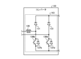
- FIG. 1 is a first diagram showing a rectification/boosting portion of a converter included in a power conversion device according to a first embodiment
- FIG. 2 is a second diagram showing a rectification/boosting portion of a converter included in a power conversion device according to the first embodiment
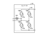
- FIG. 3 is a third diagram showing a rectification step-up portion of a converter included in a power conversion device according to the first embodiment
- FIG. 4 is a fourth diagram showing a rectification step-up portion of a converter included in a power conversion device according to the first embodiment
- FIG. 1 is a diagram showing a configuration example of a power conversion device according to a first embodiment
- FIG. 1 is a first diagram showing a rectification/boosting portion of a converter included in a power conversion device according to a first embodiment
- FIG. 2 is a second diagram showing a rectification/boosting portion of a converter included in
- FIG. 5 is a diagram showing a rectification and boosting portion of a converter included in a power conversion device according to a first embodiment.
- FIG. 1 is a diagram showing an example of a hardware configuration for implementing a control unit included in a power conversion device according to a first embodiment;
- FIG. 13 is a diagram showing an example of turn-on Joule loss, turn-on current, and turn-on voltage when the SW speed of the SW element of the inverter is slowed down in the power conversion device according to the first embodiment.
- FIG. 13 is a diagram showing an example of turn-on joule loss, turn-on current, and turn-on voltage when the SW speed of the SW element of the inverter is increased in the power conversion device according to the first embodiment;
- FIG. 1 is a diagram showing an example of a hardware configuration for implementing a control unit included in a power conversion device according to a first embodiment
- FIG. 13 is a diagram showing an example of turn-on Joule loss, turn-on current, and
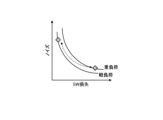
- FIG. 1 is a diagram showing an example of the relationship between noise and SW loss generated in a typical SW element.
- FIG. 1 is a first diagram showing an effect obtained by changing the SW speed of a SW element of an inverter in a power conversion device according to a first embodiment
- FIG. 2 is a second diagram showing an effect obtained by changing the SW speed of the SW element of the inverter in the power conversion device according to the first embodiment
- FIG. 1 is a diagram showing a configuration example of a waveform shape change unit provided in an inverter of a power conversion device according to a first embodiment;
- FIG. 1 is a first diagram showing a relationship between a gate current output by a waveform shape changing unit and a gate voltage indicating a rise speed of a SW element in a power conversion device according to a first embodiment
- FIG. 2 is a second diagram showing the relationship between the gate current output by the waveform shape changing unit and the gate voltage indicating the rise speed of the SW element in the power conversion device according to the first embodiment
- FIG. 3 is a third diagram showing the relationship between the gate current output by the waveform shape changing unit and the gate voltage indicating the rise speed of the SW element in the power conversion device according to the first embodiment
- FIG. 1 is a first diagram showing a relationship between a gate current output by a waveform shape changing unit and a gate voltage indicating a rise speed of a SW element in a power conversion device according to a first embodiment
- FIG. 2 is a second diagram showing the relationship between the gate current output by the waveform shape changing unit and the gate voltage indicating the rise speed of the SW element in the power conversion device according to the first embodiment
- FIG. 1 is a diagram showing an example of the relationship between a basic pulse output by a basic pulse generating unit and a gate current output by a waveform shape changing unit in a power conversion device according to a first embodiment;
- FIG. 1 is a diagram showing an example of a waveform shape setting value that a waveform shape setting unit of a power conversion device according to the first embodiment transmits to a waveform shape changing unit;
- FIG. 1 is a diagram showing a first example of a set value of a driving capability set by a waveform shape setting unit of a power conversion device according to a first embodiment;
- FIG. 13 is a diagram showing a second example of the set value of the driving capacity set by the waveform shape setting unit of the power conversion device according to the first embodiment
- FIG. 13 is a diagram showing a third example of the set value of the driving capacity set by the waveform shape setting unit of the power conversion device according to the first embodiment
- FIG. 13 is a diagram showing a fourth example of the set value of the driving capacity set by the waveform shape setting unit of the power conversion device according to the first embodiment
- FIG. 5 is a diagram showing a fifth example of the set value of the driving capacity set by the waveform shape setting unit of the power conversion device according to the first embodiment.
- FIG. 6 is a diagram showing a sixth example of the set value of the driving capacity set by the waveform shape setting unit of the power conversion device according to the first embodiment
- FIG. 1 is a diagram showing a configuration example of a power conversion device according to a second embodiment
- FIG. 13 is a diagram showing a configuration example of a power conversion device according to a third embodiment
- FIG. 13 is a diagram showing a configuration example of a refrigeration cycle application device according to a fourth embodiment.
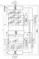
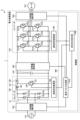
- FIG. 1 is a diagram showing a configuration example of a power conversion device 1 according to a first embodiment.
- the power conversion device 1 is connected to a commercial power source 110 and a motor 314.
- the power conversion device 1 converts a first AC power of a power source voltage supplied from the commercial power source 110 into a second AC power having a desired amplitude and phase, and supplies the second AC power to the motor 314.
- the commercial power source 110 is a single-phase AC power source in the example of FIG. 1, but may be a three-phase AC power source.
- the power conversion device 1 includes state quantity detection units 501 to 503, a converter 130, a capacitor 210, an inverter 310, and a control unit 400.
- the power conversion device 1 and the motor 314 constitute a motor drive device 2.
- the state quantity detection unit 501 detects state quantities that indicate the operating state of the power conversion device 1.
- the state quantity detection unit 501 detects, for example, the voltage value of the AC power supplied from the commercial power source 110 to the converter 130, the current value of the AC power supplied from the commercial power source 110 to the converter 130, etc.
- the converter 130 is a power converter that converts the AC power of the power supply voltage supplied from the commercial power supply 110 into DC power.
- the converter 130 includes rectifier elements 131-134, a reactor 135, a SW element 136, a freewheeling diode 137, a diode 138, and a drive circuit 150.
- the converter 130 has a bridge circuit formed by the rectifier elements 131-134, rectifies the first AC power of the power supply voltage supplied from the commercial power supply 110, boosts the rectified voltage, and outputs it.
- the drive circuit 150 generates a drive signal for actually driving the SW element 136 based on a basic pulse generated by a basic pulse generating unit 410 of the control unit 400 described later.
- the SW element 136 is, for example, an IGBT, a MOSFET (Metal Oxide Semiconductor Field Effect Transistor), a bipolar transistor, etc., but is not limited to these.
- the converter 130 includes a rectifier section 161 of a bridge circuit including rectifier elements 131 to 134, and a boost section 162 including a reactor 135, a switch element 136, a freewheel diode 137, and a diode 138, but the configuration of the converter 130 is not limited to the example of FIG. 1.
- FIG. 2 is a first diagram showing a rectifier boost section of the converter 130 included in the power conversion device 1 according to the first embodiment.
- FIG. 3 is a second diagram showing a rectifier boost section of the converter 130 included in the power conversion device 1 according to the first embodiment.
- FIG. 4 is a third diagram showing a rectifier boost section of the converter 130 included in the power conversion device 1 according to the first embodiment.
- FIG. 5 is a fourth diagram showing a rectifier boost section of the converter 130 included in the power conversion device 1 according to the first embodiment.
- FIG. 6 is a fifth diagram showing a rectifier boost section of the converter 130 included in the power conversion device 1 according to the first embodiment.
- the converter 130 may be configured to include a rectifier boost unit 163 consisting of a reactor 135, SW elements 136a and 136b, freewheel diodes 137a and 137b, and rectifier elements 133 and 134, as shown in FIG. 2.
- the rectifier boost unit 163 shown in FIG. 2 is a totem-pole bridgeless circuit.
- the converter 130 may be configured to include a rectifier boost unit 163 consisting of a reactor 135, SW elements 136b and 136d, freewheel diodes 137b and 137d, and rectifier elements 131 and 133, as shown in FIG. 3.
- the rectifier boost unit 163 shown in FIG. 3 is a half-bridgeless circuit.
- the converter 130 may be configured to include a rectifier boost unit 163 consisting of a reactor 135, SW elements 136a to 136d, and freewheel diodes 137a to 137d, as shown in FIG. 4.
- the rectifying boost unit 163 shown in Fig. 4 is a full-bridgeless circuit.
- the converter 130 may be configured to include a rectifying unit 161 including rectifying elements 131 to 134, and a boost unit 162 including reactors 135a and 135b, SW elements 136a and 136b, freewheel diodes 137a and 137b, and diodes 138a and 138b, as shown in Fig. 5.
- the boost unit 162 shown in Fig. 5 is an interleaved circuit.
- the converter 130 may be configured to include a rectifying boost unit 163 including a reactor 135, a first rectifying circuit including rectifying elements 131 to 134, a SW element 136, a freewheel diode 137, and a second rectifying circuit including rectifying elements 131a to 134a, as shown in Fig. 6.
- the rectifier boost unit 163 shown in FIG. 6 is a simple PAM (Pulse Amplitude Modulation) circuit in which a first rectifier circuit and a second rectifier circuit are connected in parallel, a SW element 136 is connected to the output terminal of the first rectifier circuit, and a capacitor 210 that supplies a second DC voltage to the inverter 310 is connected to the output terminal of the second rectifier circuit.
- PAM Pulse Amplitude Modulation
- the converter 130 has a rectifier 161 that converts the first AC voltage supplied from the commercial power source 110 into a first DC voltage, and a booster 162 that boosts the first DC voltage to a second DC voltage greater than the first DC voltage, or a rectifier booster 163 that rectifies the first AC voltage and boosts it to a second DC voltage with an effective value greater than the effective value of the first AC voltage.
- the commercial power source 110 is a three-phase AC power source
- the converter 130 is configured to include at least six elements such as rectifier elements and SW elements.
- the power conversion device 1 may be a three-phase three-wire power conversion device or a three-phase four-wire power conversion device. In this paper, the converter 130 only needs to have a rectifier function and does not need to have a boost function. In the following, the power conversion device 1 will be described using the configuration shown in FIG. 1 as an example.
- Capacitor 210 is connected to the output terminal of converter 130 and smoothes the DC power converted by converter 130.
- Capacitor 210 is, for example, an electrolytic capacitor, a film capacitor, etc.
- the state quantity detection unit 502 detects a state quantity that indicates the operating state of the power conversion device 1. For example, the state quantity detection unit 502 detects the bus voltage, which is the voltage value of the DC voltage applied from the capacitor 210 to the inverter 310.
- the inverter 310 is a power converter connected to both ends of the capacitor 210.
- the inverter 310 has SW elements 311a to 311f and freewheel diodes 312a to 312f.
- the inverter 310 turns on and off the SW elements 311a to 311f under the control of the control unit 400, and converts the power output from the converter 130 and the capacitor 210 into a second AC power having a desired amplitude and phase, i.e., generates the second AC power and outputs it to the motor 314.
- the SW elements 311a to 311f are, for example, IGBTs, MOSFETs, bipolar transistors, etc., but are not limited to these.
- the circuit configuration of the inverter 310 is not particularly limited, and may be a full bridge circuit, a single-phase bridge circuit, a half bridge circuit, etc.
- the inverter 310 also includes a waveform shape change unit 340 that can change the waveform shape of the SW waveforms of the SW elements 311a to 311f.
- the function and operation of the waveform shape change unit 340 will be described later.
- the state quantity detection unit 503 detects state quantities that indicate the operating state of the power conversion device 1.
- the state quantity detection unit 503 detects, for example, the voltage value of the second AC power supplied from the inverter 310 to the motor 314, which is the load, the current value of the second AC power supplied from the inverter 310 to the motor 314, which is the load, etc.
- the control unit 400 acquires the state quantities detected by the state quantity detection units 501-503 from the state quantity detection units 501-503, and controls the operation of the converter 130 and the inverter 310 based on the acquired state quantities; specifically, it controls the on/off of the SW element 136 of the converter 130, and controls the on/off of the SW elements 311a-311f of the inverter 310.
- the control unit 400 includes a basic pulse generation unit 410 and a waveform shape setting unit 420.
- the basic pulse generating unit 410 has a duty ratio according to the state quantity detected by the state quantity detecting units 501 to 503, and generates a basic pulse for controlling the operation of the SW element 136 of the converter 130.
- the basic pulse generating unit 410 also has a duty ratio according to the state quantity detected by the state quantity detecting units 501 to 503, and generates a basic pulse for controlling the operation of the SW elements 311a to 311f of the inverter 310.
- the basic pulse is, for example, a PWM (Pulse Width Modulation) signal having a duty ratio according to the state quantity detected by the state quantity detecting units 501 to 503.
- the basic pulse generating unit 410 outputs a basic pulse for controlling the operation of the SW element 136 of the converter 130 to the converter 130, and outputs a basic pulse for controlling the operation of the SW elements 311a to 311f of the inverter 310 to the waveform shape setting unit 420.
- the waveform shape setting unit 420 sets the waveform shape of the SW waveform of the SW elements 311a to 311f when the SW waveform of the SW elements 311a to 311f is changed by the waveform shape changing unit 340 of the inverter 310.
- the set value of the waveform shape of the SW waveform can be set separately for turn-on characteristics and turn-off characteristics.
- the waveform shape setting unit 420 outputs a control signal to reflect the set value indicating the set waveform shape.
- the waveform shape setting unit 420 controls the magnitude of the drive signal that the waveform shape changing unit 340 of the inverter 310 actually outputs to the SW elements 311a to 311f to drive the SW elements 311a to 311f and the timing of outputting the drive signal when turning on and off the SW elements 311a to 311f based on the basic pulse for controlling the operation of the SW elements 311a to 311f of the inverter 310 generated by the basic pulse generating unit 410 and the device information described later.
- the waveform shape setting unit 420 outputs a control signal to the waveform shape modification unit 340 for controlling the operation of the waveform shape modification unit 340.
- control unit 400 may be configured to have a waveform shape setting unit 420 for each waveform shape modification unit 340, i.e., six waveform shape setting units 420.
- the control unit 400 acquires the state quantities detected by the state quantity detection units 501 to 503 from the state quantity detection units 501 to 503, and controls the operation of the converter 130 and the inverter 310 based on the acquired state quantities, but this is not limited to this.
- the control unit 400 can control the operation of the converter 130 and the inverter 310 based on the state quantities acquired from at least one of the state quantity detection units 501 to 503.
- the state quantity detection units 501 to 503 detect the voltage or current input to each component of the power conversion device 1, the voltage or current output from each component of the power conversion device 1, etc. as state quantities in the above example, but the detection target is not limited to these.
- the detection target may be the frequency of the voltage input or output to each component of the power conversion device 1, the modulation rate of the voltage input to each component of the power conversion device 1, or the voltage or current of the SW elements 311a to 311f.
- the detection target may be a command value determined by the control unit 400 of the power conversion device 1.
- the installation positions of the state quantity detection units 501-503 are not limited to the example in FIG. 1.
- the power conversion device 1 does not need to have all of the state quantity detection units 501-503 arranged as in FIG. 1.
- the power conversion device 1 may have the state quantity detection unit anywhere as long as the state quantities can be detected at positions other than those shown in the figure.
- the power conversion device 1 may have a state quantity detection unit at a position where it can detect state quantities such as noise generated by the power conversion device 1, motor 314, etc., losses generated by the power conversion device 1, motor 314, etc., and the temperature of each component of the power conversion device 1, motor 314, etc.
- the motor 314 is a load connected to the power conversion device 1.
- the motor 314 is, for example, a compressor motor for driving a compressor.
- the motor 314 rotates according to the amplitude and phase of the second AC power supplied from the inverter 310, and performs a compression operation.
- the load torque of the motor 314 that drives the compressor can often be considered as a constant torque load.
- the motor 314 may be Y-connected or ⁇ -connected, or may be capable of switching between Y-connection and ⁇ -connection, for the motor windings (not shown).
- the load connected to the power conversion device 1, i.e., the inverter 310 is not limited to the motor 314 for driving a compressor, and may be a fan motor or the like.
- the load connected to the power conversion device 1 is not limited to the motor 314, and may be a load other than the motor 314.
- the power conversion device 1 can change the waveform shape of the SW waveforms of the SW elements 311a to 311f of the inverter 310 by the waveform shape setting unit 420 and the waveform shape changing unit 340. Specifically, the power conversion device 1 can change the SW speed, delay time, etc. of the SW elements 311a to 311f of the inverter 310.
- FIG. 7 is a diagram showing an example of a hardware configuration for implementing the control unit 400 provided in the power conversion device 1 according to the first embodiment.
- the above-mentioned functions and the functions described below regarding the control unit 400 can be implemented by a processor 91 and a memory 92 as shown in FIG. 7.
- the processor 91 is a CPU (also called a Central Processing Unit, processing unit, arithmetic unit, microprocessor, microcomputer, processor, or DSP (Digital Signal Processor)) or a system LSI (Large Scale Integration).
- Examples of the memory 92 include non-volatile or volatile semiconductor memories such as RAM (Random Access Memory), ROM (Read Only Memory), flash memory, EPROM (Erasable Programmable Read Only Memory), and EEPROM (registered trademark) (Electrically Erasable Programmable Read Only Memory).
- the memory 92 is not limited to these, and may be a magnetic disk, optical disk, compact disk, mini disk, or DVD (Digital Versatile Disc).
- the memory 92 stores programs that execute the functions of the control unit 400.
- the processor 91 transmits and receives necessary information via an interface that includes an analog-digital converter and a digital-analog converter (not shown), and executes the programs stored in the memory 92 to perform the required processing.
- the results of calculations by the processor 91 can be stored in the memory 92.
- FIG. 8 is a diagram showing an example of turn-on joule loss, turn-on current, and turn-on voltage when the SW speed of the SW elements 311a to 311f of the inverter 310 is slowed down in the power conversion device 1 according to embodiment 1.
- FIG. 9 is a diagram showing an example of turn-on joule loss, turn-on current, and turn-on voltage when the SW speed of the SW elements 311a to 311f of the inverter 310 is fast in the power conversion device 1 according to embodiment 1.
- A indicates turn-on joule loss
- B indicates turn-on current
- C indicates turn-on voltage.
- the horizontal axis indicates time.
- the turn-on current is the current flowing through the SW element 311a
- the turn-on voltage is the voltage applied to both ends of the SW element 311a
- the turn-on joule loss is the product of the turn-on current and the turn-on voltage
- the measurement target is not limited to the SW element 311a, and may be the other SW elements 311b to 311f.
- 8 and 9 show the difference in characteristics depending on the SW speed of SW elements 311a to 311f of inverter 310, and the specific values of "slow” and "fast” SW speeds are not important. As shown in FIGS.
- the waveform shape modification unit 340 is configured by a digital gate driver.
- the SW elements 311a to 311f of the inverter 310 and the waveform shape modification unit 340 are configured by a digital gate driver module. This allows the power conversion device 1 to change the SW speed of the SW elements 311a to 311f of the inverter 310 by changing the command value of the software without changing the hardware, and to control the noise and SW loss generated in the SW elements 311a to 311f to a desired state.
- Figure 10 is a diagram showing an example of the relationship between noise and SW loss generated in a typical SW element. As mentioned above, there is a trade-off between noise and SW loss generated in a SW element. Therefore, as shown in Figure 10, in a typical SW element, increasing the SW speed increases the noise but decreases the SW loss, and decreasing the SW speed decreases the noise but increases the SW loss.
- Figure 11 is a first diagram showing the effect obtained by changing the SW speed of SW elements 311a to 311f of inverter 310 in power conversion device 1 according to embodiment 1. Even if power conversion device 1 is operating within the noise range specified for the product in which power conversion device 1 is installed, when the load state of motor 314 changes from a light load to a heavy load, the curve showing the characteristics of noise and SW loss generated by SW elements 311a to 311f shifts to the upper right as shown in Figure 11, resulting in an increase in noise. That is, in power conversion device 1, the heavier the load, the greater the noise. Therefore, power conversion device 1 can reduce the noise generated by SW elements 311a to 311f by slowing down the SW speed of SW elements 311a to 311f.
- the power conversion device 1 can reduce the SW loss generated in the SW elements 311a to 311f by increasing the SW speed of the SW elements 311a to 311f.
- the waveform shape setting unit 420 changes the waveform shape of the SW waveform of the SW elements 311a to 311f so that the noise generated in the SW elements 311a to 311f meets the specified requirements while reducing the SW losses generated in the SW elements 311a to 311f.
- the waveform shape setting unit 420 changes the waveform shape of the SW waveform of the SW elements 311a to 311f so that the noise generated in the SW elements 311a to 311f meets the specified requirements while reducing the losses generated in the SW elements 311a to 311f.
- FIG. 12 is a second diagram showing the effect obtained by changing the SW speed of the SW elements 311a to 311f of the inverter 310 in the power conversion device 1 according to the first embodiment.
- the power conversion device 1 specifically the waveform shape changer 340, divides, for example, the turn-on period or turn-off period into two or more periods in one SW operation of the SW elements 311a to 311f, and changes the amplitude of the gate current or gate voltage for the SW elements 311a to 311f to a different magnitude in each divided period.
- the power conversion device 1 can obtain the characteristics of noise and SW loss generated by the SW elements 311a to 311f that could not be obtained with a general SW element as shown in FIG. 10.
- FIG. 13 is a diagram showing an example of the configuration of the waveform shape modification unit 340 provided in the inverter 310 of the power conversion device 1 according to embodiment 1.
- Figure 13 is also a diagram showing an example of the configuration of one digital gate driver module formed by the waveform shape modification unit 340 and the SW element 311a.
- the waveform shape change unit 340 is included in the inverter 310, which is a power converter including the SW element 311a, as shown in FIG. 1.
- the waveform shape change unit 340 includes n P-channel MOSFETs (PMOS) 1 to n as turn-on transistors, n PreDrivers for operating the n PMOS 1 to n, n N-channel MOSFETs (NMOS) 1 to n as turn-off transistors, and n PreDrivers for operating the n NMOS 1 to n.
- PMOS P-channel MOSFETs
- NMOS N-channel MOSFETs
- the waveform shape changing unit 340 is connected to a control power supply Vdd and a ground GND.
- the waveform shape changing unit 340 changes the number of PMOS1 to n or NMOS1 to n to be operated based on a control signal from the waveform shape setting unit 420, thereby changing the amplitude value of the gate current I G , which is a drive signal output to the SW element 311a, into n different values during each of the turn-on period and the turn-off period, and can adjust the SW speed of the SW element 311a.
- the waveform shape changing unit 340 can increase the absolute value of the gate current I G output to the SW element 311a as the number of PMOS1-n or NMOS1-n operated increases, and can increase the SW speed of the SW element 311a. Also, the waveform shape changing unit 340 can adjust the SW speed of the SW element 311a more finely as the number of PMOS1-n and NMOS1-n provided therein increases, and the faster the response to the increase and decrease in the gate current I G , the more finely the gate current I G can be adjusted in one SW period.
- the control signal to the waveform shape changing unit 340 may be an analog signal or a digital signal, as long as it is possible to change the number of PMOS1-n or NMOS1-n operated by the waveform shape changing unit 340.
- m parallel control signals are shown to the waveform shape modification unit 340, but this is just an example, and the number of control signals is not limited to m.
- the number of control signals may be any number that can indicate whether PMOS1-n and NMOS1-n are operational or not, or it may be possible to have only one control signal if it is an analog signal that indicates a voltage or the like.
- the waveform shape change unit 340 may be configured so that the SW characteristics of the SW elements 311a to 311f can be set individually, or so that the SW characteristics of the SW elements 311a to 311f can be set collectively.
- FIG. 14 is a first diagram showing the relationship between the gate current I G output by the waveform shape modification unit 340 in the power conversion device 1 according to the first embodiment and the gate voltage V G indicating the rising speed of the SW element 311a.
- FIG. 15 is a second diagram showing the relationship between the gate current I G output by the waveform shape modification unit 340 in the power conversion device 1 according to the first embodiment and the gate voltage V G indicating the rising speed of the SW element 311a.
- the waveform shape modification unit 340 can make the rising speed of the gate voltage V G faster, that is, the SW speed of the SW element 311a faster, as the gate current I G outputted is increased. Also, as shown in FIG. 14 and FIG.
- the waveform shape modification unit 340 can make the rising speed of the gate voltage V G slower, that is, the SW speed of the SW element 311a slower, as the gate current I G outputted is decreased.
- the power conversion device 1 can reduce the output gate current I G to slow down the SW speed when it is desired to reduce noise generated in the SW element 311a, and can increase the output gate current I G to speed up the SW speed when it is desired to reduce loss generated in the SW element 311a, as shown in Fig. 11.
- the waveforms of the gate current I G and gate voltage V G shown in Figs. 14 and 15 are ideal examples, and in reality, it takes time for the gate current I G to reach a constant current value, as shown in Figs. 8 and 9.
- FIG. 16 is a third diagram showing the relationship between the gate current I G output by the waveform shape modification unit 340 in the power conversion device 1 according to the first embodiment and the gate voltage V G indicating the rising speed of the SW element 311a.
- the waveform shape modification unit 340 can divide the turn-on period and change the magnitude of the gate current I G in each period. That is, the waveform shape modification unit 340 can finely adjust the magnitude of the gate current I G in one turn-on period.
- the power conversion device 1 can perform control to reduce the loss generated in the SW element 311a while reducing the noise generated in the SW element 311a, as shown in FIG. 12, compared to the case where the same gate current I G is output during the turn-on period.
- Fig. 17 is a diagram showing an example of the relationship between the basic pulse output by the basic pulse generating unit 410 and the gate current I G output by the waveform shape changing unit 340 in the power conversion device 1 according to the first embodiment.
- the waveform shape changing unit 340 may divide the period during which the gate current I G is output during the turn-on period of the SW element 311a, and may first output the gate current I G of the current Ig2 with a large amplitude and then output the gate current I G of the current Ig1 with a small amplitude, or may first output the gate current I G of the current Ig1 with a small amplitude and then output the gate current I G of the current Ig2 with a large amplitude.
- the waveform shape modification section 340 may divide the period during which the gate current I G is output during the turn-off period of the SW element 311 a, and first output the gate current I G of a large amplitude current -Ig2 and then output the gate current I G of a small amplitude current -Ig1, or first output the gate current I G of a small amplitude current -Ig1 and then output the gate current I G of a large amplitude current -Ig2.
- the waveform shape modification unit 340 can divide at least one of the turn-on period and the turn-off period of the SW element 311a into two or more periods and change the amplitude of the gate current I G for the SW element 311a to a different magnitude in each divided period, based on the control signal output from the waveform shape setting unit 420. Furthermore, the waveform shape modification unit 340 includes a plurality of transistors, and can change the amplitude of the gate current I G by changing the number of transistors to be operated.
- the waveform shape changing unit 340 can change the output pattern of the gate current I G for each SW cycle of the SW element 311a.
- the waveform shape changing unit 340 can change the SW waveform to a different waveform shape for each SW cycle of the SW element 311a during operation of the power conversion device 1.
- the waveform shape setting unit 420 can change the set value of the waveform shape of the SW waveform of the SW element 311a at the same cycle as the SW cycle of the SW element 311a.
- the waveform shape setting unit 420 may change the set value of the waveform shape of the SW waveform of the SW element 311a at a cycle that is a positive integer multiple of the SW cycle of the SW element 311a.
- the configuration of the waveform shape modification unit 340 shown in FIG. 13 is merely an example and is not limited to this. In this way, the waveform shape modification unit 340 can adjust the SW speed of the SW element 311a more finely by digital control using multiple MOS, compared to analog control in which the gate resistance is physically switched. Furthermore, the waveform shape modification unit 340 may use transistors other than MOS transistors for the transistors used internally.
- the waveform shape change unit 340 changes the number of PMOS or NMOS to be operated according to the acquired control signal, and outputs the gate current I G according to the number of PMOS or NMOS to be operated to the SW element 311a, but this is not limited to the above.
- the waveform shape change unit 340 may store an output pattern of the gate current I G according to the control signal, i.e., a waveform shape, in advance, and output the gate current I G in an output pattern, i.e., a waveform shape, according to the acquired control signal.
- the waveform shape change unit 340 may store a control signal acquired in the past and an output pattern, i.e., a waveform shape of the gate current I G when the control signal was acquired in the past, and output the gate current I G in the output pattern, i.e., a waveform shape stored when the same control signal was acquired.
- the waveform shape change unit 340 can reduce the processing load when outputting the gate current I G by storing the output pattern, i.e., a waveform shape, of the gate current I G according to the control signal.
- the waveform shape changing unit 340 adjusts the SW speed of the SW element 311a by changing the gate current I G as the drive signal output to the SW element 311a, and changes the waveform shape of the SW waveform of the SW element 311a, but is not limited to this.
- the waveform shape changing unit 340 sets the drive signal output to the SW element 311a as the gate voltage V G , and by changing the gate voltage V G , it can similarly adjust the SW speed of the SW element 311a and change the waveform shape of the SW waveform of the SW element 311a.
- the waveform shape modification unit 340 can divide at least one of the turn-on period and the turn-off period of the SW element 311a into two or more periods and change the amplitude of the gate voltage V G for the SW element 311a to a different magnitude in each divided period based on the control signal output from the waveform shape setting unit 420. Furthermore, the waveform shape modification unit 340 includes a plurality of transistors, and can change the amplitude of the gate voltage V G by changing the number of transistors to be operated based on the control signal output from the waveform shape setting unit 420.
- the waveform shape modification unit 340 may adjust the dead time set in the opening and closing operation of the SW elements 311a to 311f. Specifically, when the SW speed is changed, if the changed SW speed is set to be faster than the SW speed before the change, the waveform shape modification unit 340 sets the changed dead time to be shorter than the dead time before the change. Furthermore, if the changed SW speed is set to be slower than the SW speed before the change, the waveform shape modification unit 340 sets the changed dead time to be longer than the dead time before the change. In this way, the dead time can be appropriately adjusted, thereby reducing the effect of voltage error caused by the dead time.
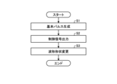
- FIG. 18 is a flowchart used to explain the operation of changing the waveform shape of the SW waveforms of the SW elements 311a to 311f in the power conversion device 1 according to the first embodiment.
- the basic pulse generation unit 410 generates a basic pulse for driving the SW elements 311a to 311f of the inverter 310 based on the state quantities acquired from the state quantity detection units 501 to 503 (step S1).
- the basic pulse generation unit 410 generates a basic pulse based on the state quantities acquired from the state quantity detection units 501 to 503, and determines the timing to turn on and off the SW elements 311a to 311f.
- the basic pulse generation unit 410 outputs the generated basic pulse to the waveform shape setting unit 420.
- the waveform shape setting unit 420 sets the waveform shape of the SW waveform at the timing to turn on and off the SW elements 311a to 311f determined by the basic pulse generating unit 410 based on the basic pulse acquired from the basic pulse generating unit 410 and the device information described below.
- the waveform shape setting unit 420 outputs a control signal to the waveform shape changing unit 340 that can change the magnitude and output timing of the drive signal according to the set waveform shape, i.e., the set value of the waveform shape (step S2).
- the waveform shape changing unit 340 changes the waveform shape of the gate current I G output to the SW elements 311a to 311f of the inverter 310, i.e., the waveform shape of the SW waveform of the SW elements 311a to 311f, based on the control signal obtained from the waveform shape setting unit 420 (step S3).
- the waveform shape changing unit 340 outputs the gate current I G after the waveform shape change to the SW elements 311a to 311f of the inverter 310.
- the waveform shape setting unit 420 outputs a control signal capable of changing the magnitude and output timing of the drive signal according to the waveform shape setting value set for the waveform shape modification unit 340.
- the waveform shape setting unit 420 may include the waveform shape setting value itself in the control signal together with the basic pulse acquired from the basic pulse generation unit 410 and transmit it to the waveform shape modification unit 340.
- FIG. 19 is a diagram showing an example of a waveform shape setting value transmitted by the waveform shape setting unit 420 of the power conversion device 1 according to the first embodiment to the waveform shape changing unit 340.
- the drive capacity setting value is an example of a waveform shape setting value.
- the drive capacity is a measure indicating the degree of the current supply capacity or power supply capacity from the waveform shape changing unit 340 to the SW element 311a.
- the drive capacity setting value is a setting value for changing the waveform shape of the SW waveform of the SW element 311a to a desired waveform shape. The larger the setting value, the higher the drive capacity.
- the information shown in FIG. 19 can be stored in the memory 92 shown in FIG. 7.
- setting value 1 is a setting value in which the number of operating MOSs is 1 and the number of non-operating MOSs is n-1.
- the number of operating MOSs means the number of pairs of PMOS1-n or NMOS1-n that are turned on or off in the waveform shape modification unit 340 in FIG. 13, and the number of non-operating MOSs means the number of pairs of PMOS1-n or NMOS1-n that are always turned off in the waveform shape modification unit 340 in FIG. 13.
- setting value 1 is a setting value that turns one PMOS/NMOS pair on or off.
- setting value 2 is a setting value that turns two PMOS/NMOS pairs on or off
- setting value 3 is a setting value that turns three PMOS/NMOS pairs on or off
- setting value n is a setting value that turns n PMOS/NMOS pairs, i.e., all PMOS/NMOS pairs on or off.
- set value 1 is the set value that produces the gentlest rise in the waveform shape
- set value n is the set value that produces the steepest rise in the waveform shape.
- the waveform shape modification unit 340 when a setting value of 1 is sent from the waveform shape setting unit 420, the waveform shape modification unit 340 turns on or off only one arbitrary PMOS/NMOS pair, and does not operate the other n-1 PMOS/NMOS pairs, keeping them always off. The same applies to setting values 2 and 3. Also, when a setting value of n is sent from the waveform shape setting unit 420, the waveform shape modification unit 340 turns on or off all PMOS/NMOS pairs. Note that if the waveform shape modification unit 340 has a storage unit, the storage unit may have a table that indicates which PMOS/NMOS pairs are operated and which PMOS/NMOS pairs are not operated, corresponding to the drive capacity setting value.
- each PMOS/NMOS pair is the same for each pair, that is, if one of the PMOS/NMOS pairs operates, the other also operates, but the operating PMOS/NMOS may be different pairs.
- the operation information, command value information, and status information of the power conversion device 1 are collectively referred to as "device information.”
- the operation information of the power conversion device 1 is information related to the operation of a product equipped with the power conversion device 1.
- the operation information includes information such as heating operation, cooling operation, fan operation, demagnetization sequence, preheating operation, and protective operation.
- the demagnetization sequence is a control sequence that demagnetizes the residual magnetic flux of the current sensor before normal operation.
- An example of the current sensor referred to here is a current transformer that is assumed to be present in the state quantity detection unit 503. Note that the current sensor provided in the state quantity detection unit 503 is a sensor used to control the motor 314 for driving the compressor, and is not a sensor that is newly provided for the control of the power conversion device 1 according to the first embodiment.
- Preheating operation is an operation mode in which the refrigerant is preheated during operation, i.e., before cooling operation, heating operation, etc.
- Protective operation is an operation mode in which the torque command for controlling the motor 314 is lowered compared to normal operation when the power conversion device 1 is, for example, in an overload state.
- the refrigeration cycle-applied equipment receives input of a heating operation command, a cooling operation command, or a fan operation command from a controller such as a remote control or an operation panel, and performs heating operation, cooling operation, or fan operation based on these input commands.
- the refrigeration cycle-applied equipment performs a degauss sequence, preheating operation, or protective operation based on input commands such as a degauss sequence command, preheating operation command, or protective operation command generated inside the control unit 400.
- the command value information of the power conversion device 1 is information related to command values that operate the power converter.
- the command value information includes information such as an AC output voltage command value, an AC output current command value, and an AC output frequency command value, which are command values that operate the power converter. Note that these AC output voltage command value, AC output current command value, and AC output frequency command value are examples, and other command value information may be included.
- the status information of the power conversion device 1 is information that indicates the operating state of the power converter, and environmental information when the power converter or the power conversion device 1 is operating.
- the status information includes information such as element module temperature, equipment temperature, cooler temperature, motor temperature, motor mechanical angle phase, and motor electrical angle phase. This information is listed with the intention of utilizing detection information from existing sensors, and there is no particular intention to install new sensors.
- the status information includes information such as the inside air temperature and the outside air temperature.
- the inside air temperature is the temperature of the air-conditioned space
- the outside air temperature is the temperature of the outside air.
- the above-mentioned device information i.e., the operation information, command value information, and status information of the power conversion device 1
- the control unit 400 without providing a special detection unit or sensor.
- the power conversion device 1 according to the first embodiment aims to make it possible to change the waveform shape of the SW waveform while suppressing an increase in the circuit scale in the waveform shape change unit 340 by utilizing this device information.
- the power conversion device 1 if the above-mentioned device information is used, it becomes unnecessary to input the state quantities detected by the state quantity detection units 501 to 503 to the waveform shape setting unit 420 as shown in FIG. 1. Therefore, if the device information is used, the amount of processing in the waveform shape setting unit 420 can be reduced. This makes it possible to use a less expensive processor for the control unit 400.
- Each of the control modes shown in Figs. 20 to 25 utilizes at least one piece of device information, and is implemented by transmitting the setting value of the driving capacity set by the waveform shape setting unit 420 based on the device information to the waveform shape changing unit 340.
- FIG. 20 is a diagram showing a first example of the set value of the driving capacity set by the waveform shape setting unit 420 of the power conversion device 1 according to the first embodiment.
- the horizontal axis of FIG. 20 indicates the command value, and the vertical axis indicates the set value of the driving capacity.
- Examples of the command value are an AC output voltage command value or an AC output current command value. Either of these command values is used when generating a basic pulse inside the control unit 400.
- FIG. 20 shows a control curve when the bus voltage is high and the surge voltage is suppressed. When the bus voltage is high, if the command value becomes large, there is a risk that the surge voltage will exceed the allowable value. For this reason, the waveform shape setting unit 420 performs control in accordance with the control curve of FIG. 20 to reduce the set value of the driving capacity as the command value becomes larger.
- FIG. 21 is a diagram showing a second example of the drive capacity setting value set by the waveform shape setting unit 420 of the power conversion device 1 according to the first embodiment.
- the horizontal and vertical axes are the same as those in FIG. 20.
- FIG. 21 shows a control curve when the bus voltage is low and SW loss or noise is suppressed.
- the bus voltage is low, there is often a margin in the tolerance for surge voltage.
- the waveform shape setting unit 420 performs control such that the drive capacity setting value is increased as the command value increases, in accordance with the control curve in FIG. 21.
- FIG. 22 is a diagram showing a third example of the set value of the driving capacity set by the waveform shape setting unit 420 of the power conversion device 1 according to the first embodiment.
- the horizontal axis of FIG. 22 indicates the AC output current command value
- the vertical axis indicates the set value of the driving capacity.
- FIG. 22 also shows five control curves corresponding to the operation information, namely, heating operation, cooling operation, fan operation, demagnetization sequence, and preheating and protection operation. As in FIG. 20, these control curves are used when the bus voltage is high and the surge voltage is to be suppressed. When the bus voltage is high, if the AC output current command value increases, the surge voltage may exceed the allowable value.
- the waveform shape setting unit 420 performs control to reduce the set value of the driving capacity as the AC output current command value increases, according to the control curve of FIG. 22, based on the operation information and the AC output current command value.
- the influence of the AC output current command value is small, since the operation is short, there is no need to increase the set value of the driving capacity, and there is no need to change the set value of the driving capacity according to the absolute value of the temperature difference.
- FIG. 23 is a diagram showing a fourth example of the set value of the driving capacity set by the waveform shape setting unit 420 of the power conversion device 1 according to the first embodiment.
- the horizontal axis of FIG. 23 indicates the absolute value of the temperature difference, and the vertical axis indicates the set value of the driving capacity.
- An example of the absolute value of the temperature difference is the absolute value of the difference between the inside air temperature and the outside air temperature.
- FIG. 23 also shows four control curves corresponding to the operation information, namely, cooling and heating operation, fan operation, demagnetization sequence, and preheating and protection operation. As in FIG. 20 and FIG. 22, these control curves are used when the bus voltage is high and the surge voltage is to be suppressed.
- the surge voltage is affected by the absolute value of the temperature difference.
- the absolute value of the temperature difference the smaller the power required for air conditioning, so the set value of the driving capacity can be increased accordingly.
- the influence of the absolute value of the temperature difference is small, and the power required during operation is smaller than in heating operation and cooling operation, so the set value of the driving capacity can be set larger than in heating operation and cooling operation.
- the influence of the absolute value of the temperature difference is small, and the operation is for a short time, so as in FIG.
- the physical quantity shown on the horizontal axis of FIG. 23 may be temperature instead of the absolute temperature difference. If the temperature is, for example, the element module temperature, the equipment temperature, the cooler temperature, or the motor temperature, increasing the drive capacity setting may cause these temperatures to exceed the allowable value. For this reason, when the air conditioner is in cooling or heating operation, the drive capacity setting is controlled to be decreased as the temperature increases.
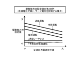
- FIG. 24 is a diagram showing a fifth example of the set value of the driving capacity set by the waveform shape setting unit 420 of the power conversion device 1 according to the first embodiment.
- the horizontal axis of FIG. 24 indicates the AC output frequency command value
- the vertical axis indicates the set value of the driving capacity and the bus voltage.
- the control curve indicates the set value of the driving capacity. This control curve is used to suppress the surge voltage when the load state of the power conversion device 1 is a heavy load.
- the bus voltage depends on the AC output frequency command value, and the bus voltage increases as the AC output frequency command value increases. For this reason, if the AC output frequency command value increases, there is a risk that the surge voltage will exceed the allowable value. Therefore, the waveform shape setting unit 420 performs control to reduce the set value of the driving capacity as the AC output frequency command value increases according to the control curve in FIG. 24.
- FIG. 25 is a diagram showing a sixth example of the set value of the driving capacity set by the waveform shape setting unit 420 of the power conversion device 1 according to the first embodiment.
- the horizontal and vertical axes are the same as those in FIG. 24.
- the control curve shows the set value of the driving capacity. This control curve is used to suppress noise when the load state of the power conversion device 1 is light.
- the curve of the bus voltage is the same as that shown in FIG. 24.
- the waveform shape setting unit 420 performs control to increase the set value of the driving capacity as the AC output frequency command value increases according to the control curve in FIG. 25.
- control curves are shown as continuous straight lines in Figs. 20 to 25, the set values of the driving capabilities are integer values, so the control curves shown in Figs. 20 to 25 may be set in a stepped manner. Also, if the values corresponding to the control curves include decimal values, the decimal portion may be rounded up, down, or rounded off.
- the power conversion device includes a waveform shape setting unit and a waveform shape changing unit.
- the waveform shape setting unit sets the waveform shape of the SW waveform of the SW element of the inverter based on device information, which is operation information, command value information, or status information of the power conversion device.
- the waveform shape changing unit changes the waveform shape of the SW waveform of the SW element of the inverter based on the setting value of the waveform shape set by the waveform shape setting unit, without physically switching the gate resistor.
- the waveform shape setting unit may set the waveform shape setting value based on at least command value information, may set the waveform shape setting value based on at least state information, or may set the waveform shape setting value based on at least operation information.
- the waveform shape setting value is the driving capability setting value.
- the driving capability is a measure indicating the degree of current supply capability or power supply capability from the waveform shape changing unit to the SW element.
- Embodiment 2 In the first embodiment, a case has been described in which the waveform shape of the SW waveform of the SW elements 311a to 311f of the inverter 310 is changed in the power conversion device 1. In the second embodiment, a case has been described in which the waveform shape of the SW waveform of the SW element 136 of the converter 130 is changed in the power conversion device 1.
- FIG. 26 is a diagram showing an example of the configuration of the power conversion device 1 according to the second embodiment.
- the power conversion device 1 is connected to a commercial power source 110 and a motor 314.
- the power conversion device 1 converts a first AC voltage of the power source voltage supplied from the commercial power source 110, which is an AC power source, into a second AC voltage having a desired amplitude and phase, and supplies the second AC voltage to the motor 314.
- the power conversion device 1 includes state quantity detection units 501-503, a converter 130, a capacitor 210, an inverter 310, and a control unit 400.
- the power conversion device 1 and the motor 314 form a motor drive device 2.
- the power conversion device 1 of the second embodiment shown in FIG. 26 is obtained by removing the waveform shape change unit 340 from the inverter 310 and adding a drive circuit 350 to the power conversion device 1 of the first embodiment shown in FIG. 1, and by removing the drive circuit 150 from the converter 130 and adding a waveform shape change unit 140 to the converter 130.
- the power conversion device 1 of the second embodiment shown in FIG. 26 also changes the output destinations of the basic pulse generation unit 410 and the waveform shape setting unit 420 from the power conversion device 1 of the first embodiment shown in FIG. 1.
- the basic pulse generation unit 410 outputs a basic pulse for controlling the operation of the SW element 136 of the converter 130 to the waveform shape setting unit 420, and outputs a basic pulse for controlling the operation of the SW elements 311a to 311f of the inverter 310 to the inverter 310.
- the drive circuit 350 In the inverter 310, the drive circuit 350 generates a drive signal for actually driving the SW elements 311a to 311f based on the basic pulse generated by the basic pulse generating unit 410 of the control unit 400.
- the waveform shape setting unit 420 performs the operation described in the first embodiment.
- the waveform shape modification unit 140 performs the same operation as the waveform shape modification unit 340 described in the first embodiment.
- the power conversion device 1 performs the same operation as in the first embodiment, and thereby the waveform shape setting unit 420 and the waveform shape modification unit 140 can change the waveform shape of the SW waveform of the SW element 136 of the converter 130.
- the converter has the functions of the power conversion device according to the first embodiment. This makes it possible to obtain the same effects as in the first embodiment in the converter.
- Embodiment 3 In the first embodiment, a case has been described in which the waveform shape of the SW waveform of the SW elements 311a to 311f of the inverter 310 is changed in the power conversion device 1. In the second embodiment, a case has been described in which the waveform shape of the SW waveform of the SW element 136 of the converter 130 is changed in the power conversion device 1. In the third embodiment, a case will be described in which the set value of the waveform shape of the SW waveform of the SW elements 311a to 311f of the inverter 310 is changed and the set value of the waveform shape of the SW waveform of the SW element 136 of the converter 130 is changed in the power conversion device 1.
- FIG. 27 is a diagram showing an example of the configuration of the power conversion device 1 according to the third embodiment.
- the power conversion device 1 is connected to a commercial power source 110 and a motor 314.
- the power conversion device 1 converts a first AC voltage of the power source voltage supplied from the commercial power source 110, which is an AC power source, into a second AC voltage having a desired amplitude and phase, and supplies it to the motor 314.
- the power conversion device 1 includes state quantity detection units 501-503, a converter 130, a capacitor 210, an inverter 310, and a control unit 400.
- the power conversion device 1 and the motor 314 form a motor drive device 2.
- the power conversion device 1 of the third embodiment shown in FIG. 27 is obtained by removing the drive circuit 150 from the converter 130 and adding a waveform shape changing unit 140 to the power conversion device 1 of the first embodiment shown in FIG. 1.
- the power conversion device 1 of the third embodiment shown in FIG. 27 also changes the output destinations of the basic pulse generating unit 410 and the waveform shape setting unit 420 compared to the power conversion device 1 of the first embodiment shown in FIG. 1.
- the basic pulse generating unit 410 outputs a basic pulse for controlling the operation of the SW elements 311a to 311f of the inverter 310 to the waveform shape setting unit 420, and outputs a basic pulse for controlling the operation of the SW element 136 of the converter 130 to the waveform shape setting unit 420.
- the waveform shape setting unit 420 performs the operation described in the first embodiment as well as the operation described in the second embodiment.
- the waveform shape modification unit 340 performs the same operation as that described in the first embodiment
- the waveform shape modification unit 140 performs the same operation as that described in the second embodiment.
- the power conversion device 1 performs the same operation as in the first embodiment, thereby being able to change the waveform shape of the SW waveform of the SW elements 311a to 311f of the inverter 310 by the waveform shape setting unit 420 and the waveform shape modification unit 340.
- the power conversion device 1 performs the same operation as in the second embodiment, thereby being able to change the waveform shape of the SW waveform of the SW element 136 of the converter 130 by the waveform shape setting unit 420 and the waveform shape modification unit 140.
- the power conversion device 1 can also control one of the waveform shape change units 140, 340 to change the waveform shape of the SW waveform of the SW element at a certain timing, and the other not to change the waveform shape of the SW waveform of the SW element.
- the SW elements for which the waveform shape change units 140, 340 of the power conversion device 1 change the SW waveform are one or more SW elements included in at least one of the one or more power converters that perform power conversion in the power conversion device 1.
- the inverter and converter have the functions of the power conversion device according to the first embodiment. This makes it possible to enjoy the same effects as in the first embodiment in both the inverter and the converter.
- Fig. 28 is a diagram showing a configuration example of a refrigeration cycle-applied device 900 according to embodiment 4.
- the refrigeration cycle-applied device 900 according to embodiment 4 includes the power conversion device 1 described in embodiment 1.
- the refrigeration cycle-applied device 900 according to embodiment 4 can also include the power conversion device 1 described in embodiment 2 and embodiment 3.
- the refrigeration cycle-applied device 900 according to embodiment 4 can be applied to products equipped with a refrigeration cycle, such as air conditioners, refrigerators, freezers, and heat pump water heaters.
- components having the same functions as those in embodiment 1 are denoted by the same reference numerals as those in embodiment 1.
- the refrigeration cycle application device 900 includes a compressor 315 incorporating the motor 314 in the first embodiment, a four-way valve 902, an indoor heat exchanger 906, an expansion valve 908, and an outdoor heat exchanger 910, which are attached via a refrigerant pipe 912.
- a compression mechanism 904 that compresses the refrigerant, and a motor 314 that operates the compression mechanism 904.
- the refrigeration cycle device 900 can perform heating or cooling operation by switching the four-way valve 902.
- the compression mechanism 904 is driven by a variable speed controlled motor 314.
- the refrigerant is pressurized by the compression mechanism 904 and sent out, passes through the four-way valve 902, the indoor heat exchanger 906, the expansion valve 908, the outdoor heat exchanger 910, and the four-way valve 902, and returns to the compression mechanism 904.
- the refrigerant is pressurized by the compression mechanism 904 and sent out, passes through the four-way valve 902, the outdoor heat exchanger 910, the expansion valve 908, the indoor heat exchanger 906, and the four-way valve 902, and returns to the compression mechanism 904.
- the indoor heat exchanger 906 acts as a condenser to release heat, and the outdoor heat exchanger 910 acts as an evaporator to absorb heat.
- the outdoor heat exchanger 910 acts as a condenser to release heat, and the indoor heat exchanger 906 acts as an evaporator to absorb heat.
- the expansion valve 908 reduces the pressure of the refrigerant to expand it.
- the refrigeration cycle-applied equipment 900 can reduce the noise generated by the SW elements 311a to 311f, etc., by slowing down the SW speed of the SW elements 311a to 311f, etc.
- the refrigeration cycle device 900 can reduce losses generated by the SW elements 311a to 311f by increasing the switching speed of the SW elements 311a to 311f.
- the digital gate driver module constituted by the waveform shape change unit 340 and SW elements 311a to 311f included in the inverter 310 generates a large surge voltage and a lot of electromagnetic noise when the SW speed is fast.
- the refrigeration cycle application device 900 uses a flammable refrigerant, there is a possibility that the refrigerant may burn due to discharge caused by electromagnetic noise when the refrigerant leaks. Therefore, the refrigeration cycle application device 900 sets the SW speed of the digital gate driver module provided in the power conversion device 1 according to the flammability of the refrigerant used in the refrigeration cycle application device 900.
- the refrigeration cycle application device 900 slows down the SW speed of the digital gate driver module provided in the power conversion device 1 the higher the flammability of the refrigerant used in the refrigeration cycle application device 900.
- the refrigeration cycle device 900 can reduce surge voltage by slowing down the switching speed of the digital gate driver module, and by suppressing the occurrence of discharges caused by electromagnetic noise, it is possible to prevent combustion even if refrigerant leaks from the refrigeration cycle device 900.
- the refrigerant used in the refrigeration cycle application equipment 900 is, for example, any one of R1234yf, R1234ze(E), R1243zf, HFO1123, HFO1132(E), R1132a, CF3I, and R290, or a mixed refrigerant containing at least two of the above refrigerants.
- 1 Power conversion device 2 Motor drive device, 91 Processor, 92 Memory, 110 Commercial power source, 130 Converter, 131-134, 131a-134a Rectifier element, 135, 135a, 135b Reactor, 136, 136a-136d, 311a-311f SW element, 137, 137a-137d, 312a-312f Freewheel diode, 138, 138a, 138b Diode, 140, 340 Waveform shape change unit, 150, 350 drive circuit, 161 rectifier, 162 booster, 163 rectifier booster, 210 capacitor, 310 inverter, 314 motor, 315 compressor, 400 control unit, 410 basic pulse generator, 420 waveform shape setting unit, 501-503 state quantity detector, 900 refrigeration cycle applicable device, 902 four-way valve, 904 compression mechanism, 906 indoor heat exchanger, 908 expansion valve, 910 outdoor heat exchanger, 912 refrigerant piping, GND ground.
Landscapes
- Engineering & Computer Science (AREA)
- Power Engineering (AREA)
- Inverter Devices (AREA)
Priority Applications (2)
| Application Number | Priority Date | Filing Date | Title |
|---|---|---|---|
| PCT/JP2023/038025 WO2025083881A1 (ja) | 2023-10-20 | 2023-10-20 | 電力変換装置、モータ駆動装置及び冷凍サイクル適用機器 |
| JP2025552582A JPWO2025083881A1 (https=) | 2023-10-20 | 2023-10-20 |
Applications Claiming Priority (1)
| Application Number | Priority Date | Filing Date | Title |
|---|---|---|---|
| PCT/JP2023/038025 WO2025083881A1 (ja) | 2023-10-20 | 2023-10-20 | 電力変換装置、モータ駆動装置及び冷凍サイクル適用機器 |
Publications (1)
| Publication Number | Publication Date |
|---|---|
| WO2025083881A1 true WO2025083881A1 (ja) | 2025-04-24 |
Family
ID=95448844
Family Applications (1)
| Application Number | Title | Priority Date | Filing Date |
|---|---|---|---|
| PCT/JP2023/038025 Pending WO2025083881A1 (ja) | 2023-10-20 | 2023-10-20 | 電力変換装置、モータ駆動装置及び冷凍サイクル適用機器 |
Country Status (2)
| Country | Link |
|---|---|
| JP (1) | JPWO2025083881A1 (https=) |
| WO (1) | WO2025083881A1 (https=) |
Citations (6)
| Publication number | Priority date | Publication date | Assignee | Title |
|---|---|---|---|---|
| JP2004096318A (ja) * | 2002-08-30 | 2004-03-25 | Mitsubishi Electric Corp | 電力用半導体装置 |
| JP2009027881A (ja) * | 2007-07-23 | 2009-02-05 | Toyota Motor Corp | 半導体スイッチング素子の駆動制御装置 |
| JP2011082764A (ja) * | 2009-10-06 | 2011-04-21 | Mitsubishi Electric Corp | パワーデバイス制御回路およびそれを用いたipm |
| JP2014011817A (ja) * | 2012-06-27 | 2014-01-20 | Denso Corp | 電力変換装置 |
| JP2017028900A (ja) * | 2015-07-24 | 2017-02-02 | 株式会社デンソー | 電力変換器制御装置 |
| WO2021245719A1 (ja) * | 2020-06-01 | 2021-12-09 | 三菱電機株式会社 | パワー半導体素子の駆動制御装置、及び、パワーモジュール |
-
2023
- 2023-10-20 WO PCT/JP2023/038025 patent/WO2025083881A1/ja active Pending
- 2023-10-20 JP JP2025552582A patent/JPWO2025083881A1/ja active Pending
Patent Citations (6)
| Publication number | Priority date | Publication date | Assignee | Title |
|---|---|---|---|---|
| JP2004096318A (ja) * | 2002-08-30 | 2004-03-25 | Mitsubishi Electric Corp | 電力用半導体装置 |
| JP2009027881A (ja) * | 2007-07-23 | 2009-02-05 | Toyota Motor Corp | 半導体スイッチング素子の駆動制御装置 |
| JP2011082764A (ja) * | 2009-10-06 | 2011-04-21 | Mitsubishi Electric Corp | パワーデバイス制御回路およびそれを用いたipm |
| JP2014011817A (ja) * | 2012-06-27 | 2014-01-20 | Denso Corp | 電力変換装置 |
| JP2017028900A (ja) * | 2015-07-24 | 2017-02-02 | 株式会社デンソー | 電力変換器制御装置 |
| WO2021245719A1 (ja) * | 2020-06-01 | 2021-12-09 | 三菱電機株式会社 | パワー半導体素子の駆動制御装置、及び、パワーモジュール |
Also Published As
| Publication number | Publication date |
|---|---|
| JPWO2025083881A1 (https=) | 2025-04-24 |
Similar Documents
| Publication | Publication Date | Title |
|---|---|---|
| AU2014203525B2 (en) | Converter circuit and motor drive control apparatus, air-conditioner, refrigerator, and induction heating cooker provided with the circuit | |
| US4736595A (en) | Circuit for controlling inventer in air conditioner | |
| JP2012200042A (ja) | インバータ制御装置及び冷凍空調装置 | |
| WO2016027357A1 (ja) | 電動機駆動装置及びこれを用いた空気調和装置あるいは冷凍空調装置 | |
| US11323050B2 (en) | Power supply apparatus | |
| JP7045529B2 (ja) | 電力変換装置および空気調和機 | |
| WO2025083881A1 (ja) | 電力変換装置、モータ駆動装置及び冷凍サイクル適用機器 | |
| WO2023238296A1 (ja) | 電力変換装置、モータ駆動装置及び冷凍サイクル適用機器 | |
| KR20070077632A (ko) | 공기조화기 및 그 제어방법 | |
| WO2025083875A1 (ja) | 電力変換装置、モータ駆動装置及び冷凍サイクル適用機器 | |
| WO2025083879A1 (ja) | 電力変換装置、モータ駆動装置及び冷凍サイクル適用機器 | |
| WO2025083877A1 (ja) | 電力変換装置、モータ駆動装置および冷凍サイクル適用機器 | |
| WO2025083880A1 (ja) | 電力変換装置、モータ駆動装置及び冷凍サイクル適用機器 | |
| WO2025083882A1 (ja) | 電力変換装置、モータ駆動装置および冷凍サイクル適用機器 | |
| WO2025083876A1 (ja) | 電力変換装置、モータ駆動装置および冷凍サイクル適用機器 | |
| WO2025083884A1 (ja) | 電力変換装置、モータ駆動装置および冷凍サイクル適用機器 | |
| JP7825712B2 (ja) | 電力変換装置および冷凍サイクル適用機器 | |
| JP7630643B2 (ja) | 電力変換装置、モータ駆動装置及び冷凍サイクル適用機器 | |
| WO2025083883A1 (ja) | 電力変換装置、モータ駆動装置および冷凍サイクル適用機器 | |
| WO2023238293A1 (ja) | 空気調和機 | |
| WO2025083878A1 (ja) | 電力変換装置、モータ駆動装置および冷凍サイクル適用機器 | |
| JP7241968B2 (ja) | 空気調和機 | |
| KR20010037408A (ko) | 인버터 공기조화기의 실외팬제어방법 | |
| WO2023243003A1 (ja) | 電力変換装置、モータ駆動装置及び冷凍サイクル適用機器 | |
| KR100395945B1 (ko) | 인버터 공기조화기의 캐리어주파수제어방법 |
Legal Events
| Date | Code | Title | Description |
|---|---|---|---|
| 121 | Ep: the epo has been informed by wipo that ep was designated in this application |
Ref document number: 23956128 Country of ref document: EP Kind code of ref document: A1 |
|
| ENP | Entry into the national phase |
Ref document number: 2025552582 Country of ref document: JP Kind code of ref document: A |
|
| WWE | Wipo information: entry into national phase |
Ref document number: 2025552582 Country of ref document: JP |